silicon grating couplers for low loss …fsoptics/thesis/wirth__justin_ms.pdf · 2.1.1 overview ......
TRANSCRIPT
SILICON GRATING COUPLERS FOR LOW LOSS COUPLING BETWEEN
OPTICAL FIBER AND SILICON NANOWIRES
A Thesis
Submitted to the Faculty
of
Purdue University
by
Justin C. Wirth
In Partial Fulfillment of the
Requirements for the Degree
of
Master of Science in Electrical and Computer Engineering
December 2011
Purdue University
West Lafayette, Indiana
ii
ACKNOWLEDGMENTS
I would like to thank Prof. Andrew Weiner and Prof. Minghao Qi for introducing
me to research as an undergraduate student, and for guiding and mentoring me along this
process. Additionally, my thanks go out to all of my very helpful group mates, and
particularly to Leo T. Varghese, Li Fan, and Dan Leaird, without whom this work would
not have been possible. I would also like to thank my wonderful family for their love and
support.

iii
TABLE OF CONTENTS
Page
LIST OF TABLES ...............................................................................................................v
LIST OF FIGURES ........................................................................................................... vi
ABSTRACT ....................................................................................................................... ix
1. INTRODUCTION ....................................................................................................... 1
1.1 Narrative of the Problem ...................................................................................... 11.2 Objective and Overview ....................................................................................... 4
2. GRATING COUPLER SIMULATION AND DESIGN ............................................. 5
2.1 Grating Coupler Theory and Operation ............................................................... 52.1.1 Overview ................................................................................................. 52.1.2 Coupling theory ....................................................................................... 62.1.3 Curved grating couplers ........................................................................... 7
2.2 Simulation Methods ............................................................................................. 92.2.1 Design and simulation constraints ........................................................... 92.2.2 CAMFR ................................................................................................. 102.2.3 Validity check ........................................................................................ 12
2.3 Effects of Design Parameters ............................................................................. 142.3.1 Buried oxide layer .................................................................................. 142.3.2 Silicon top layer ..................................................................................... 152.3.3 Grating etch depth and the polynomial fit method ................................ 162.3.4 Grating periodicity ................................................................................. 192.3.5 Fill factor ............................................................................................... 212.3.6 Coupling angle ....................................................................................... 222.3.7 Summary of parameter effects ............................................................... 23
2.4 Optimized Grating Design ................................................................................. 24
iv
Page
3. EXPERIMENTAL DESIGN ..................................................................................... 27
3.1 In-Coupling and Out-Coupling .......................................................................... 273.1.1Fiber v-groove array ............................................................................... 27 3.1.2 Precision stage and imaging .................................................................. 30
3.2 Fabrication Process ............................................................................................ 343.3 Coupler Layout ................................................................................................... 35
4. EXPERIMENTAL CHARACTERIZATION ........................................................... 39
4.1 Characterization Setup ....................................................................................... 394.1.1 Sample inspection .................................................................................. 39
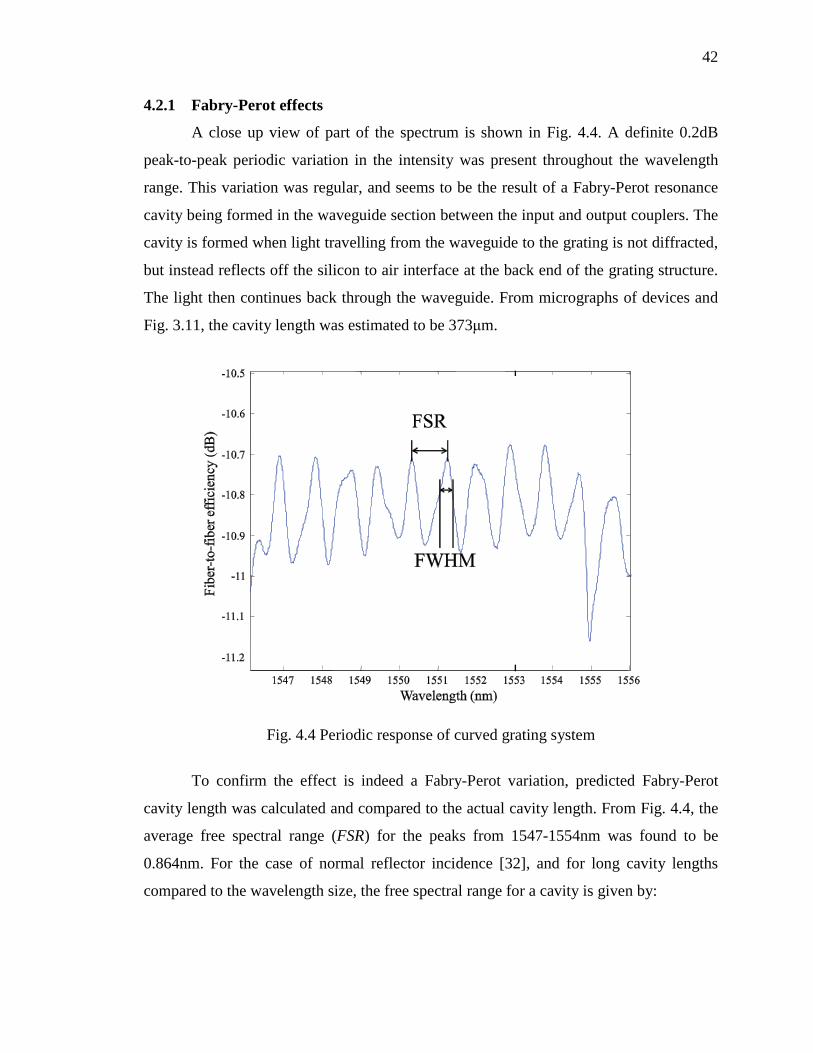
4.2 Measurement of Curved Couplers with 8˚ Silicon Substrate V-Groove Assembly 414.2.1 Fabry-Perot effects ................................................................................ 42
4.3 Measurement with 10˚ All Pyrex V-Groove Assembly ..................................... 434.3.1 Straight coupler measurements at 10˚ .................................................... 444.3.2 Curved coupler measurements at 10˚..................................................... 454.3.3 Analysis of results ................................................................................. 46
4.4 Measurement Consistency.................................................................................. 464.4.1 Input stability ......................................................................................... 474.4.2 Mechanical stability ............................................................................... 484.4.3 Coupler to chip separation ..................................................................... 494.4.4Analysis of measurement consistency .................................................... 50
4.5 Device Consistency ............................................................................................ 514.6 Comparison of Experimental Results With Goals and Published Results ......... 53
5. PRACTICAL APPLICATION .................................................................................. 54
5.1 Three-Port Ring Resonator Coupled Devices in Amorphous Silicon ................ 555.1.1 Device structure and operation .............................................................. 555.1.2 Ring resonator coupling gap .................................................................. 56
5.1.3 Thru and Drop port performance ........................................................... 575.2 One Dimensional Photonic Crystal Cavity ............................................................. 59
5.1.1 Device structure and operation .............................................................. 595.2.2 Cavity performance ............................................................................... 615.2.2 Coupling performance ........................................................................... 61
6. CONCLUSION AND FUTURE WORK .................................................................. 63
LIST OF REFERENCES ...................................................................................................65

v
LIST OF TABLES
Table Page
2.1 Summary of center wavelength effects of grating parameters ................................. 24
5.1 Effect of ring resonator coupling gap ....................................................................... 57
5.2 Three-port signal distribution ................................................................................... 59
vi
LIST OF FIGURES
Figure Page
1.1 Comparison of coupling scale differences .................................................................... 2
2.1 Illustration of grating coupling between optical fibers and an SOI sample .................. 5
2.2 Example focused grating structure................................................................................ 8
2.3 Differing spatial division methods of a sample grating type structure ....................... 10
2.4 Visualization of CAMFR coupling simulation ........................................................... 11
2.5 Reference coupler specifications ................................................................................ 12
2.6 Comparison of published simulation with simulated reference coupler data ............. 13
2.7 Effect of buried oxide thickness ................................................................................. 15
2.8 Effect of silicon top layer thickness ............................................................................ 16
2.9 Polynomial fitting to curve data at 80nm etch depth .................................................. 18
2.10 Comparison of the effects of grating etch depth ....................................................... 19
2.11 Comparison of the effects of grating period ............................................................. 20
2.12 Comparison of the effects of fill factor ..................................................................... 22
2.13 Effect of coupling angle ............................................................................................ 23
2.14. Optimized grating profile design ............................................................................. 24
2.15 Optimized grating coupler simulated performance ................................................... 25
2.16 Optimized grating coupler simulated fiber-to-fiber loss ........................................... 26
vii
Figure Page
3.1 Scale perspective illustration of Pyrex v-groove array ............................................... 28
3.2 Scale end facet diagram of Pyrex v-groove array ....................................................... 29
3.3 Axes of adjustment for coupling stage........................................................................ 30
3.4 V-groove array mounted to stage ................................................................................ 31
3.5 Y view of v-groove and SOI chip ............................................................................... 32
3.6 X view of v-groove and SOI chip ............................................................................... 33
3.7 Fabrication process for defining grating couplers on SOI wafers .............................. 34
3.8 Scale top profile view of straight coupler layout ........................................................ 36
3.9 Scale side profile view of straight coupler layout ....................................................... 36
3.10 Layout of straight coupling setup ............................................................................. 37
3.11 Layout of curved coupling setup............................................................................... 38
4.1 Micrographs of fabricated curved and straight couplers ............................................. 40
4.2 Micrograph of device array ......................................................................................... 40
4.3 Efficiency of curved grating system at 8˚ coupling angle .......................................... 41
4.4 Periodic response of curved grating system................................................................ 42
4.5 Efficiency of straight grating system at 10˚ coupling angle ....................................... 44
4.6 Efficiency of curved grating system at 10˚ coupling angle ........................................ 45
4.7 Effect of coupling efficiency with time ...................................................................... 47
4.8 Effect of coupling efficiency with time on fine curve features .................................. 48
4.9 Effect of mechanical realignment ............................................................................... 49
4.10 Effect on efficiency from input/output coupling distance ........................................ 50
4.11 Fine structure comparison of 5 different devices ...................................................... 51

viii
Figure Page
4.12 Coupler consistency throughout a row of 5 devices ................................................. 52
4.13 Comparison of best achieved coupling and published results for curved couplers .. 53
5.1 Three-port amorphous silicon device.......................................................................... 55
5.2 Thru and Drop port output performance ..................................................................... 57
5.3 Three-port resonant features ....................................................................................... 58
5.4 One dimensional photonic crystal cavity device layout ............................................. 60
5.5 One dimensional photonic crystal cavity bistability response .................................... 61
5.6 One dimensional photonic crystal spectrum ............................................................... 62
ix
ABSTRACT
Wirth, Justin C. M.S.E.C.E., Purdue University, December 2011. Silicon Grating Couplers for Low Loss Coupling Between Optical Fiber and Silicon Nanowires. Major Professor: Andrew M. Weiner.
The promise of silicon nanophotonic devices is constrained by the large inherent
size difference between comparatively large optical fibers and much smaller photonic
waveguides, which causes an unacceptable amount of loss without a mode size
conversion solution. One such solution is the vertical grating coupler, which allows light
to be efficiently coupled in from the top of a device. However, for standard 250nm
crystalline silicon top layers of silicon-on-insulator wafers, no such published designs
existed. The initial focus of this research was to design and test a grating coupler for
operation at 1550nm in the near infrared which could be used for coupling to photonic
devices on these wafers. Coupling quasi-TE mode polarized light at less than 10dB fiber-
to-fiber loss with a 3dB bandwidth across the C-band was required. Grating layouts were
designed and simulated, and a maximally efficient solution was found. This design was
then fabricated in both straight grating and curved grating varieties. Testing showed a
fiber-to-fiber loss as low as 9.5dB, with 43nm of 1dB bandwidth and 76nm of 3dB
bandwidth. Therefore, coupler performance exceeded the required efficiency and far
surpassed the bandwidth target. Further expanding the design to other silicon structure
types, amorphous versions of the same couplers were also fabricated. Performance was
slightly less but comparable to crystalline couplers. Both material types were
incorporated into devices and demonstrated as effective coupling solutions. Future work
will focus on increasing efficiency, utilization of the couplers’ Fabry-Perot properties,
and developing amorphous couplers for use on flexible substrates.
1
1. INTRODUCTION
1.1 Narrative of the Problem
Silicon nanophotonics is the branch of optics that involves studying and applying
the useful properties of photons in a silicon medium on the nanometer scale. Miniaturized
systems using materials also found in silicon-based electronics processing offers the
potential for small, relatively cheap to manufacture platforms on which to build photonic
devices. This is contrasted with bulk optical photonic setups, which tend to be large,
expensive, require vibration minimizing tables, and are prone to accidental misalignment.
Silicon based device components such as high Q resonant cavities [1], low loss
waveguides [2], optical buffers [3], AND and NAND logic [4], and optical modulators
[5] have all been developed. Furthermore, more complex devices accomplishing arbitrary
waveform generation [6], waveform sensing [7], chemical sensing [8], and amplification
by four wave mixing [9] and Raman scattering [10] have all been shown as well.
Additionally, the benefit of silicon over a silicon hybrid like silicon nitride is
silicon’s abundant use, availability, and higher refractive index. This higher refractive
index allows for very compact waveguides, with cross sections of 500nm by 250nm, or
smaller, possible for silicon photonic devices. This is significantly smaller than what is
possible with bulk or fiber optic system, and smaller still than possible with silicon
nitride waveguides.
This smaller size is potentially not an issue if using on-chip methods of signal
generation. However, problems arise when trying to couple light from typical infrared
fiber optic systems into and out of nanophotonic devices. A commonly used wavelength
range for photonics work is the C band, which spans from 1530nm to 1565nm. For
operation at 1550nm, which is near the middle of the C band, typical optical fiber
confines the single mode optical signal to a 10.4 m mode field diameter [11].

2
The large inherent size mismatch between the 10.4 m typical mode diameter of
the light mode in fiber and a 500nm by 250nm rectangular silicon waveguide means that
an enormous amount of power will necessarily be lost when trying to move the signal
directly from fiber to the waveguide end. This is illustrated in Fig. 1.1. Additionally,
there exists a large numerical aperture difference between the two systems which will
similarly hamper efficiency when coupling light out of the nanophotonic device. Power is
especially important when trying to use nonlinear device effects in silicon, and the
incoming power loss can prohibit interesting nonlinearities from being expressed. Also,
this combined loss is such that it can exceed the amplification offered by fiber amplifiers,
making good signal recovery from the chip very difficult.
Fig. 1.1 Comparison of coupling scale differences
Various solutions for the coupling problem have been proposed and implemented.
One of the most simple is to use lensed fiber optic cable to focus the light down to a
smaller mode size. When properly aligned and focused, this leads to a significant
reduction in loss. Total loss from the input fiber, through the chip, and out to the output
fiber, or fiber-to-fiber loss, is reduced to around 20dB with this method. However, this is
still much higher loss than is desirable. Further efficiency gains can be had by better
matching the fiber and chip edge modes by varying the nanowire end facet geometry.
Silicon Waveguide
Fiber Core
10 m
1550nm MFD in Fiber
3
Methods such as overcladdings [12], multi-dielectric structures [13], and inverse tapers
[14] have been shown to achieve low loss. But the additional fabrication complexity in
making overcladdings and dielectric stacks tend to make them undesirable compared to
solutions that do not require new process steps. Furthermore, all of these methods require
precise chip cleaving and polishing, which are not always feasible or available.
A different approach involves launching light onto the chip vertically instead of
horizontally. This has the significant benefit of avoiding the end facet all together, and
only relies on normal process steps to produce a good structure. Vertical coupling also
eliminates the need for precise chip cleaving or polishing. Utilizing a diffraction grating
to redirect the light from near vertical incidence into the chip plane, these vertical grating
couplers have been shown to have low losses similar to other enhanced coupling methods
[15].
For research or test applications, grating couplers also allow multiple devices to
be laid out in two dimensions on the chip in a grid type pattern instead of linearly in a
row. The resulting greater density means that many more devices can be fabricated in a
single fabrication run, and this allows for much more flexibility in chip layout.
Furthermore, lensed fiber side coupling setups tend to be limited to one optical input and
output because of the necessary stage mechanics to do such sensitive alignment. Using
grating couplers with the right setup makes it possible to use many inputs and outputs at
once.
For polarization sensitive applications, the grating coupler is particularly
beneficial because it acts as a polarization filter. For the coupling design explored in this
work, light polarized parallel with the direction of the grating teeth (TE polarized light)
couples well to the grating, while almost none of the light polarized perpendicular to the
grating teeth (TM light) will be coupled into the waveguide [16]. In practice, once light is
in the silicon waveguide, it will not exist in a pure TE or TM mode, though it will
strongly resemble one or the other [17]. The waveguide mode is then called the quasi-TE
or quasi-TM mode. For structures that perform much better with the quasi-TE mode, such
as ring resonators [1], the grating coupler provides a simple and convenient way of
designing for and assuredly attaining this polarization.
4
Finally, grating couplers eliminate the need for devices that span from one side of
the chip to the other. This cuts down on waveguide loss, and allows for a Fabry-Perot
effect that has a much larger period than possible for long side coupled waveguides. This
is beneficial for devices that have weak effects on short wavelength scales, as the short
period Fabry-Perot effect that results from long waveguides will hide these.
1.2 Objective and Overview
As a result of these benefits, a grating coupler coupling system for use with
silicon nanophotonic devices was desired. The objective for this work was to design a
vertical grating coupler for coupling use with standard silicon on insulator (SOI) wafers
with 250nm crystalline silicon top layers. It was required that the coupler achieve
efficient coupling with less than 10dB fiber-to-fiber loss for the quasi-TE mode and 3dB
bandwidth over the C-band. The properties of designed couplers were tested to ensure
consistent performance. Effective test work with crystalline SOI lead to work in
amorphous SOI. Amorphous silicon has potential interesting applications in flexible
nanophotonics, and these will be discussed as potential future work. Operation of
multiple output couplers was explored in a ring resonator coupled device. However, to be
considered truly successful, demonstration was needed with an actual test nanophotonic
device. This device was a one dimensional photonic crystal, the functioning of which
requires the short waveguide length made possible by grating couplers.
This thesis covers theory and operation, as well as simulation of grating coupler
properties and subsequent design choices, in chapter 2. Chapter 3 describes design of the
experimental setup and coupler layout. Experimental results and consistency
measurements in SOI wafers are examined in chapter 4. In Chapter 5, practical devices
and application of the designed couplers are explored. This includes the demonstration of
amorphous SOI grating couplers, results from multiple output port designs, and the
successful practical application of the grating coupler’s use in coupling into and out of
one dimensional photonic crystal samples. Finally, the conclusion and future work are
addressed in chapter 6.
5
2. GRATING COUPLER SIMULATION AND DESIGN
2.1 Grating Coupler Theory and Operation
2.1.1 Overview
Grating couplers were invented in the 1970’s as a method of coupling free space
laser light into glass films [18]. The grating coupler is essentially a Bragg grating
optimized to diffract light from a free space source into a dielectric waveguide. Similarly,
a coupler can also be used to diffract light from a waveguide into a free space detector.
For the work presented here, and often for silicon photonics in general, the dielectric
waveguide is silicon on top of silicon dioxide, the free space source is replaced by a
single mode optical fiber transmitting laser light, and the free space detector replaced by
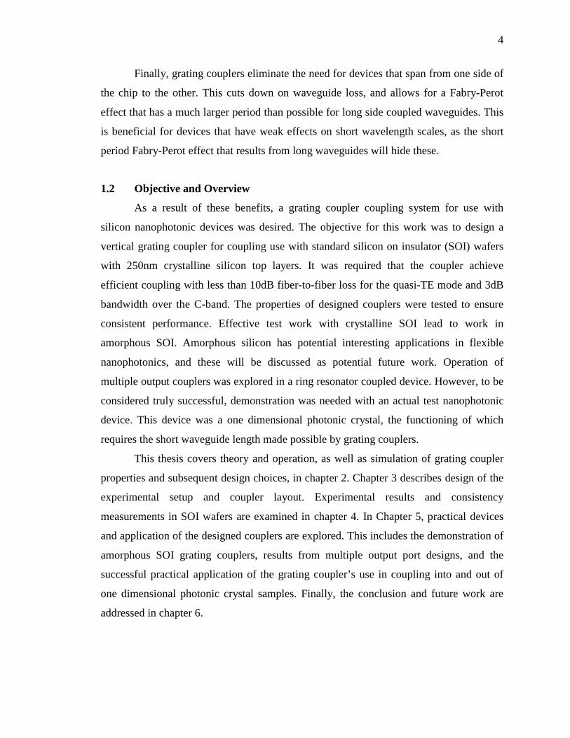
a single mode fiber to collect light. An example (not to scale) of this type of coupling
setup is shown in Fig. 2.1.
Fig. 2.1 Illustration of grating coupling between optical fibers and an SOI sample
Input
2SiO
Output
Silicon
Silicon Substrate
Silicon Dioxide
6
When used in conjunction with photonic devices, the silicon section between the
grating couplers in Fig. 2.1 will consist of two taper sections and the device section.
These taper sections are necessary, as the incoming light from the fiber has a width of
10.4 m and the nanophotonic wire commonly used for devices has a width of 500nm.
Common taper shapes include linear and parabolic, and both can achieve very low loss
size conversion. However, the necessary lengths are at least a hundred microns for
parabolic tapers [19] and many hundreds of microns for linear tapers [20].
2.1.2 Coupling theory
As a type of Bragg grating, the basic operation of a grating coupler is defined by
the Bragg condition [21]:
mnn ctopeff )sin( (2.1)
where effn is the effective refractive index of the grating, topn is the refractive index of the
material on top of the grating, c is the coupling angle measured perpendicular to the chip
surface, m is the particular diffraction mode, is the wavelength of incident light, and
is the grating period. This equation describes the modes of operation for a grating at a
particular coupling angle, but it does not give any useful information about the efficiency
of a given structure.
Although methods have been developed to calculate the coupling efficiency
between the single mode fiber and the grating coupler through only equations and
analysis [22], computer simulation is necessary to model an appropriate variety of grating
structures. Using the eigenmode expansion method [23] (further discussed in section.
2.2.2), the coupling efficiency can calculated by determining the amount of power
coupled out of the grating that couples to the Gaussian shaped fiber mode [24]. As the
width of the waveguide is much greater than either the waveguide height or the
wavelength of light, the model can be reduced to two dimensions, and can be further
reduced to one dimension with high accuracy if the width of the grating is sufficiently
long and the fiber is a constant distance from the grating. For this case, the efficiency is
given by:

7
2
)sin(2)(
0
20
20
),( dyeAezzyE ctopnjywyy
(2.2)
where A is a constant describing the normalized Gaussian beam, 0w is the beam width,
and y is the coordinate axis parallel to the waveguide axis. The value of z, being the
separation between the fiber and the top of the grating, is held constant at 0z . For a
nonzero coupling angle, this is accomplished with a polished fiber end.
While Eqn. 2.2 gives a way of finding the coupling efficiency for a grating to a
fiber, it does not contain terms for the grating structure itself. Structural parameters
include the silicon top layer height, grating period, depth, fill factor, and buried oxide
thickness, all of which have a significant effect on the coupling efficiency [25]. In fact,
they are not omitted, but appear by affecting the E(y,z) term. Using an appropriate field
modeling package, the power coupled up by the grating as a result of an incident power
in the waveguide can be calculated, and then fed into Eqn. 2.2 to get the system’s
coupling efficiency.
Although the focus thus far has been on the coupling situation from the grating
coupler to optical fiber, the reverse case is also modeled by Eqn. 2.2. This is because all
materials used are isotropic and linear, and all permittivities and permeabilities in the
system can be expressed as symmetric matrices, so the system can be said to be
reciprocal [26]. This allows the efficiency for a single grating-to-fiber case to be
simulated and applied to both grating-to-fiber interfaces to obtain the fiber-to-fiber loss of
the coupling system.
2.1.3 Curved grating couplers
In addition to linear grating couplers that taper down to the waveguide
dimensions, focused grating couplers have been developed. These use the same sort of
grating structure as straight couplers, except the gratings are specifically curved in the
wafer plane to focus light down to the dimensions of the photonic wire. When properly
curved, the light efficiently travels from the curved grating to the 500nm waveguide in as
little as 12.5 m [27]. This curvature is described (modified for correctness from [27]) by:
8
220 )sin( yxnynq effctop (2.3)
where q is a negative integer corresponding to each grating line, 0 is the vacuum center
wavelength of incoming light, is a correction factor to match the grating spacing at x=0
with results for a straight coupler, topn is the refractive index of the material on top of the
grating, effn is the effective refractive index of the grating, c is the coupling angle, x is
the coordinate axis perpendicular to the waveguide axis, y is the coordinate axis parallel
to the waveguide axis, and the origin located at the focal spot, where the waveguide
begins. An example of this sort of focused structure is shown in Fig. 2.2.
Fig. 2.2 Example focused grating structure
The advantage to this sort of structure over straight grating types is the compact
footprint the can be achieved. Additionally, these types of couplers have been shown to
have performance on the level of that of straights couplers [27].
XY
9
2.2 Simulation Methods
2.2.1 Design and simulation constraints
The grating coupler structure was designed for use with SOI wafers that our group
had access to, and were available without special order from manufacturers. These wafers
have a crystal silicon top layer of 250nm and a buried silicon dioxide layer of 3 m. To
reach the 10dB fiber-to-fiber loss target for the quasi-TE polarization mode, each end of
the coupling setup must have slightly less than 5dB loss to account for a small loss in the
waveguide, which means a required efficiency of slightly more than 32% per coupler.
Additionally, the 3dB bandwidth must be at least 40nm, and the center wavelength must
be near 1550nm.
Since the mode field diameter of 1550nm light from standard fiber is 10.4 m, the
grating coupler must be approximately this size to capture the transmitted light. In order
to couple from this large mode into the waveguide mode, a taper must be used for straight
waveguides, or a focused grating coupler must be used. At this stage, it is assumed that a
very efficient method of mode conversion can be made, and thus the focus will be on
coupler efficiency.
Grating couplers are three dimensional structures, and thus for fully accurate
simulation of conversion efficiency from the coupler to the waveguide a 3D simulation
would be necessary. However, almost all of the third dimensional aspect comes from the
taper of the larger grating width to the smaller waveguide structure, as the coupler itself is
two dimensional. For a straight coupler, the structure is two dimensional in rectangular
coordinates and uniformly extended into the third dimension. For curved couplers, the
grating structure at the center of the curve is the same as that of the straight case. For the
rest of the curve, the curvature is specified to retain the coupling efficiency seen at the
center. As such, simulation of the grating itself was approximated in two dimensions.
This approximation allowed much faster simulation, as 3D simulations take orders of
magnitude longer to do than 2D for a given amount of processing power.
10
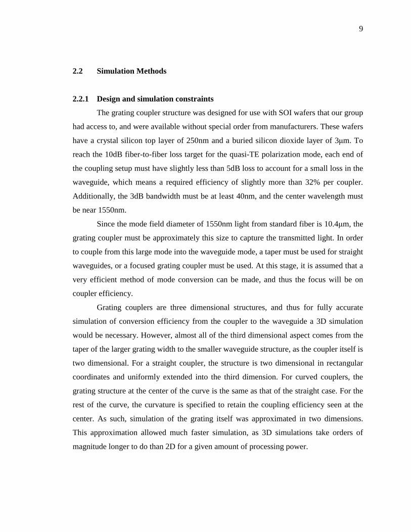
2.2.2 CAMFR
Simulation was done with the software package CAMFR, short for “Cavity
Modeling Framework” [28]. An example code from [24] based upon the principles
presented in section 2.1.2 was found and modified for modeling use. Unlike many
modeling methods that rely upon spatial discretization, such as finite element modeling
and finite-difference time-domain simulation, CAMFR makes use of eigenmode
expansion. In this method, a given geometry is separated into layers of constant refractive
index distribution. The difference in how these two methods divide a simulated geometry
is illustrated in Fig. 2.3
Fig. 2.3 Differing spatial division methods of a sample grating type structure
Using eigenmode expansion, simulation is accomplished by summing the field
eigenmodes in each layer to get the field profile in that layer. Although this requires a
number of different modes be simulated, perfectly matched layer (PML) boundary
conditions are used at the boundaries of the simulation area to allow for distinct modes
Eigenmode Expansion
Spatial Discretization
11
without the issue of boundary reflection.
This method is contrasted with spatial discretization, which requires the simulated
structure be broken up into a grid and the fields simulated at every grid point. For
accurate simulation this requires a fine grid and a corresponding large number of grid
points and simulation time. With eigenmode expansion, a small number of layers are
necessary, and the calculation time is independent of the layer length [24]. This leads to
much more efficient simulation and is particularly useful for the simulation of grating
couplers, as they are inherently layered structures.
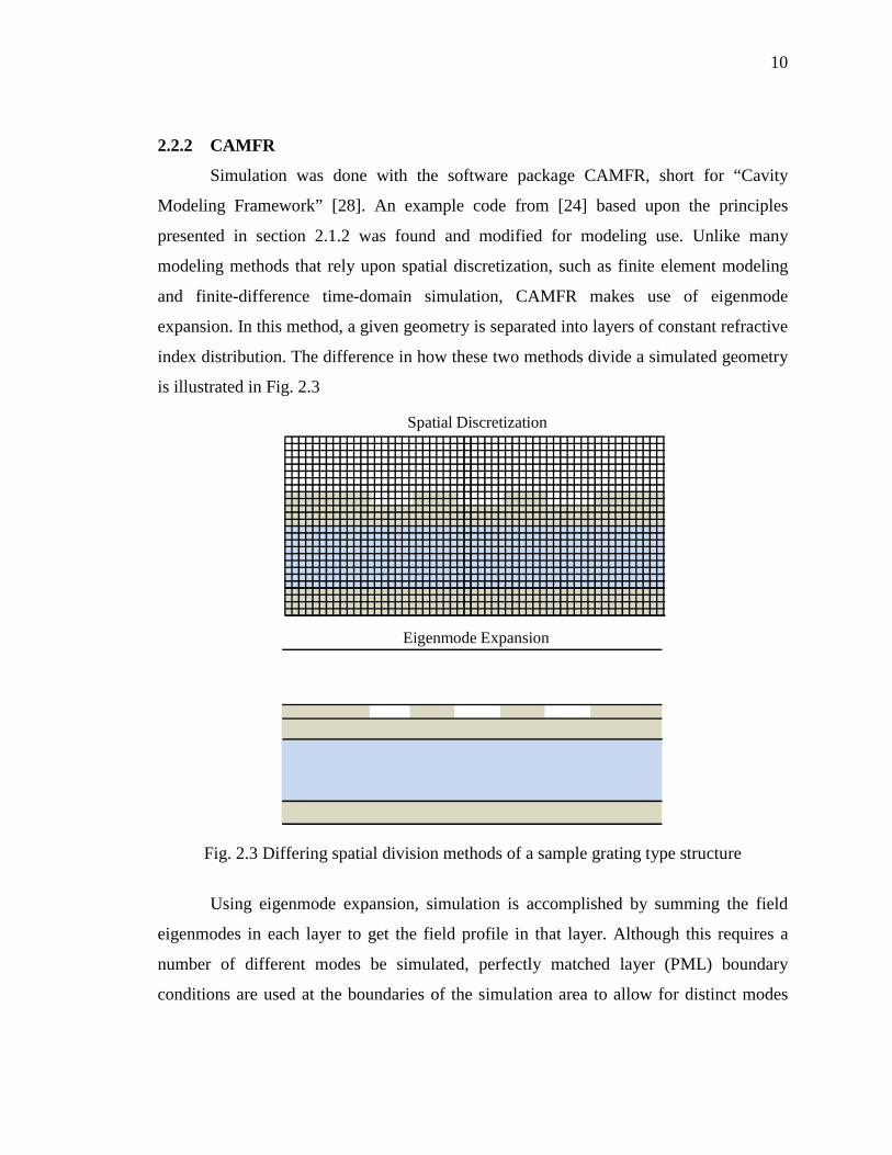
As CAMFR simulates a structure based on the incident light, simulation is done
for a specific wavelength of the incoming signal. Once all the field modes for a
wavelength have been calculated and summed, CAMFR allows the time varying field
profile to be animated and expressed visually. A snapshot of this visual representation is
shown in Fig. 2.4. The black outlines are the boundaries of the structures and material
layers, with the top most layer representing an index matched fluid. The next three layers
are the silicon top layer, silicon dioxide buffer, and silicon substrate of an SOI wafer. The
topmost silicon layer is seen to contain the grating structure. Blue and red bands show the
electric field of light as it travels from the left end of the grating to the right, being
diffracted by the grating structure along the way. The deepness of color indicates the field
intensity at the point.
Fig. 2.4 Visualization of CAMFR coupling simulation (Full view on left, expanded view on right)
In Fig. 2.4, it can be seen that the majority of the power is coupled upwards at a
particular angle, although a significant amount leaks downwards into the substrate. This
12
is a result of the negative diffraction mode, and is the cause of much of the coupler loss.
Without impractically high coupling angles [29] or complicated reflective layers under
the grating [30], this loss cannot be completely removed. However, particular thicknesses
of the oxide layer will reflect this light back up with the rest of the signal [25], and this is
the reason more field intensity is present in the oxide layer in Fig. 2.4 than the bottom
silicon layer.
Once simulation of a given structure over a set of modes and wavelengths is
complete, the coupling behavior is recorded numerically and the coupling efficiency can
be calculated. Each wavelength’s efficiency can be plotted to form an efficiency curve.
These curves are an easy way to see the characteristics of a coupler structure, such as
efficiency and bandwidth, and are the main tool for evaluating coupler performance.
2.2.3 Validity check
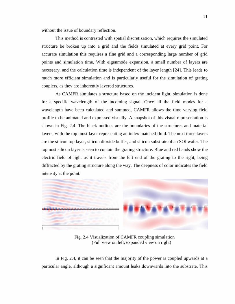
In order to check the validity of the simulation code, it was checked against a
published simulation result in [24]. The chosen reference design has somewhat close
characteristics to the SOI wafer to be used for the coupler in this research, and thus
served as a good comparison. The reference SOI wafer had a 220nm silicon top layer and
1 m of buried oxide. The reference coupler design consisted of 20 grating periods with a
630nm grating period, a 50% fill factor, and a 70nm etch depth. This is illustrated in Fig
2.5. Note that in the figure, only a few periods are shown.
Fig. 2.5 Reference coupler specifications
Si
1 m
630nm
70nm
315nm150nm 315nm
2SiO
220nm
13
These coupler dimensions were put into the simulation code. Additionally, an 8
degree tilt of the incoming light and an index matched layer above the coupler of n=1.46
were used as in the reference design. This index matched layer simulates the use of an
overcladding to match the refractive index of the fiber. This reduces the reflection
between the fiber and this intermediary layer, and also enhances coupling to the substrate.
The simulation was run at 2nm intervals from 1500nm to 1650nm, matching the range of
the published data and giving a high resolution reconstruction of it. Polarization was set
to the quasi-TE mode.
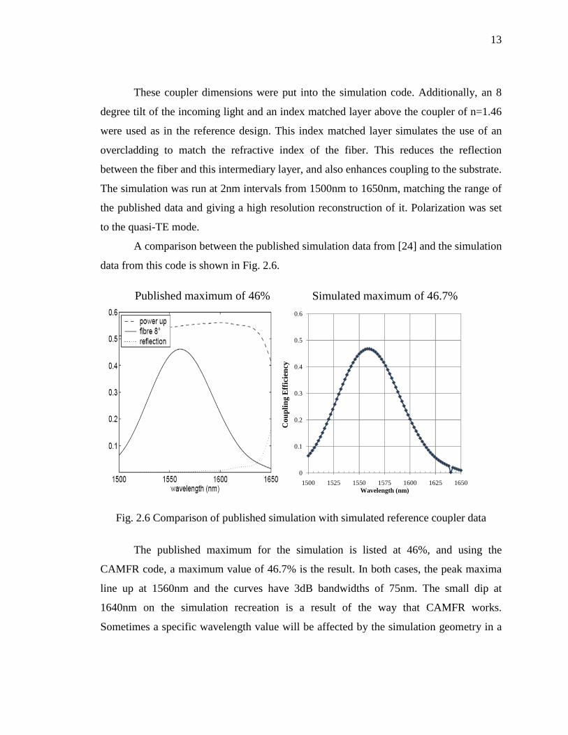
A comparison between the published simulation data from [24] and the simulation
data from this code is shown in Fig. 2.6.
Fig. 2.6 Comparison of published simulation with simulated reference coupler data
The published maximum for the simulation is listed at 46%, and using the
CAMFR code, a maximum value of 46.7% is the result. In both cases, the peak maxima
line up at 1560nm and the curves have 3dB bandwidths of 75nm. The small dip at
1640nm on the simulation recreation is a result of the way that CAMFR works.
Sometimes a specific wavelength value will be affected by the simulation geometry in a
0
0.1
0.2
0.3
0.4
0.5
0.6
1500 1525 1550 1575 1600 1625 1650Wavelength (nm)
Published maximum of 46% Simulated maximum of 46.7%C
oupl
ing
Eff
icie
ncy
14
way that greatly decreases its efficiency on the first mode run. Because the simulated
efficiency is so low in these cases (on the order of 10-7%), CAMFR stops running further
modes, and the value is effectively recorded at zero. This does not occur for wavelengths
right before or after the given wavelength, and as will be seen later, does not show up in
experimental data. This type of effect occurs essentially randomly for about 1% of data
points, and can effectively be ignored as a simulation artifact.
From the very good agreement between the published data and the data from the
simulation used here, it was concluded that the simulation code provides a very similar
model to the reference model [24]. It should be noted that in [24] (similar to [13] [15]
[19] [20] [27]), the experimental efficiency obtained was approximately 45% lower than
the simulated maximum efficiency for the ideal structure, and thus this model is not
expected to provide a perfect experimental fit.
2.3 Effects of Design Parameters
The model having been shown to be valid, simulations were done to find the
effects of the various design parameters on coupler efficiency in order to create a
maximally efficient coupler. These parameters include the depth of the silicon top layer
(TL), depth of buried oxide layer (BOX), grating periodicity (GP), grating etch depth
(ED), fill factor (FF), and coupling angle (CA). All simulations shown have an index
matched layer with n=1.46.
2.3.1 Buried oxide layer
As seen in literature [24] [25], the buried oxide layer has a large effect on the
efficiency of a grating coupler as a result of its role in reflecting light that leaks through
the coupling structure. This variation is periodic with thickness, and the difference
between using a thickness that coincides with an efficiency maximum vs. a minimum can
be as large as 37% [24]. However, neither [24] nor [25] is useful for predicting the effect
of our 3 m BOX, as simulation in both is only concerned with thinner oxide layers.
Since the oxide thickness of the wafers used in this research is fixed at 3 m, the
purpose of simulation is to check the effect of the oxide rather than to optimize it.
15
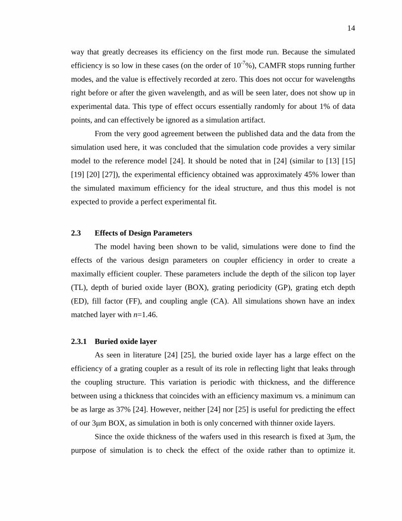
However, if the effect of the thicker BOX is a similar or larger efficiency compared to the
reference 1 m BOX, it could be taken as an indication that 3 m is very close to an
optimal value. The difference between the 3 m BOX of these wafers and those used in
the reference design is shown in Fig. 2.7.
Fig. 2.7 Effect of buried oxide thickness
As a result of increasing the BOX from 1 m to 3 m, the efficiency increased
16%. The center wavelength is slightly blue shifted from 1560nm to 1556, and the 3dB
bandwidth is decreased from 75nm to 52nm. This implies that the increased BOX should
allow for slightly more efficient coupling at the expense of some bandwidth.
2.3.2 Silicon top layer
The thickness of the silicon top layer also plays a major role in coupling
efficiency [24]. It has been shown that a top layer thickness for the grating that exceeds
the thickness of the waveguide can lead to highly increased efficiency [15]. Although this
research does not go that far in scope, the modest increase of 30nm more silicon in the
0
0.1
0.2
0.3
0.4
0.5
0.6
1500 1525 1550 1575 1600 1625 1650
Cou
plin
g Ef
ficie
ncy
Wavelength (nanometers)
220nm TL, 630nm GP, 70nm ED, 50% FF, 8˚ CA
1um BOX
3um BOX
16
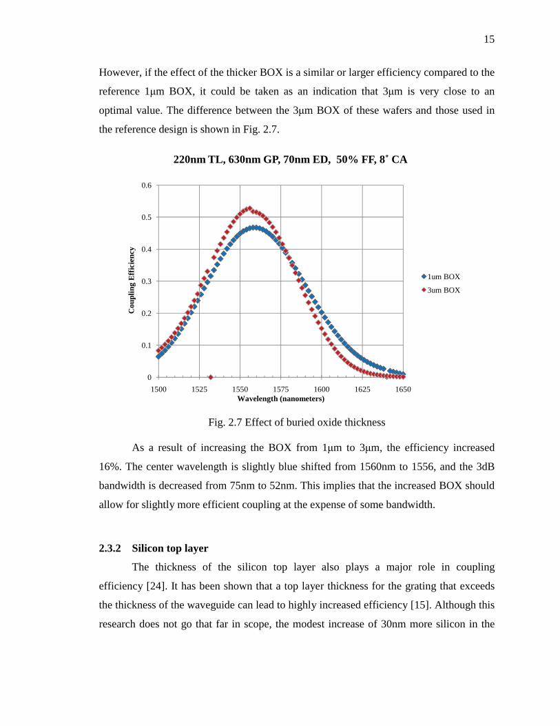
coupler should have a positive effect on performance.
This simulation was done with the 1 m BOX of the reference coupler instead of a
3 m BOX in order to see the effect of a top layer thickness increase independent of any
other parameters. The results of this are shown in Fig. 2.8.
Fig. 2.8 Effect of silicon top layer thickness
The increased top layer thickness does indeed increase the maximum efficiency,
and the result is a slight 5.5% boost. A significant red shift also occurred, moving the
peak 52nm to 1609nm. The bandwidth was unaffected. It will be seen that the slight
efficiency boost from the additional silicon can be further enhanced with grating
parameters tailored to the new thickness.
2.3.3 Grating etch depth and the polynomial fit method
The grating etch depth, grating period, and fill factor are the parameters that
actually define the grating. Whereas the top layer height and buried oxide thickness were
set by the chosen SOI wafers, these parameters must be chosen to maximize efficiency,
0
0.1
0.2
0.3
0.4
0.5
0.6
1500 1525 1550 1575 1600 1625 1650
Cou
plin
g E
ffic
ienc
y
Wavelength (nanometers)
1 m BOX, 630nm GP, 70nm ED, 50% FF, 8˚ CA
220nm TL
250nm TL
17
bandwidth, and have the correct center wavelength. Grating etch depth was the first
addressed. As the etch depth changes, the effective refractive index and the reflectivity of
the given area will also change [21]. More etching will cause a lower effective index, and
likewise less etching will cause a higher effective index. This effective index change
drives the change of the peak center wavelength
As a result of designing parameter values instead of merely checking the effect of
a single change, initial simulation of etch depth revealed a greater number of simulations
runs were necessary to accurately gauge its efficiency effect. The smooth efficiency
curve implied that a high number of points were not needed to accurately simulate the
curve behavior. Furthermore, the extreme ends of the wavelength range did not need
simulation either, as long as the center wavelength was apparent. In these cases, the
bandwidth and curve behavior were recovered from curve symmetry.
Because of to these factors, and in an effort to reduce simulation time without
reducing accuracy, the interval between data points was increased from 2nm to 15nm.
This interval was chosen as it is the largest convenient interval that keeps 3 data points in
the C-band. The extreme lowest and highest wavelength points were dropped, leaving 9
data points from 1515nm to 1635nm. A 6th order polynomial fit curve was then applied
these points. The comparison between these three representations is shown in Fig. 2.9.
18
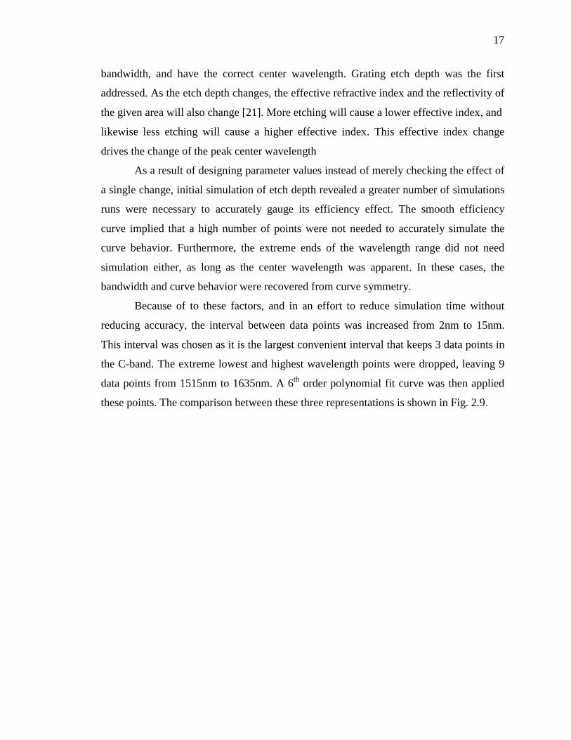
Fig. 2.9 Polynomial fitting to curve data at 80nm etch depth
It is apparent from Fig. 2.9 that the polynomial fit is extremely good. The curve
passes through the centers of all of the 2nm interval data points, and thus traces the data
in the interval from 1515 to 1635. The curve is not extended beyond this range as it
begins to deviate from the data, but the efficiency is so low at these sections that they are
essentially irrelevant. The very good accuracy of this simulation came at an eighth of the
simulation time. A polynomial fit is used here for simulating etch depth behavior and is
indicated by a solid line on the graph rather than discrete data points. For subsequent
graphs in this thesis, solid lines in simulation graphs will similarly indicate use of the
polynomial fit.
Simulation of etch depth parameters took place for depths of 60nm to 140nm in
10nm increments. 10nm was chosen as the increment size as it was deemed a reasonable
level of accuracy that could be achieved through reactive ion etch (RIE) in the fabrication
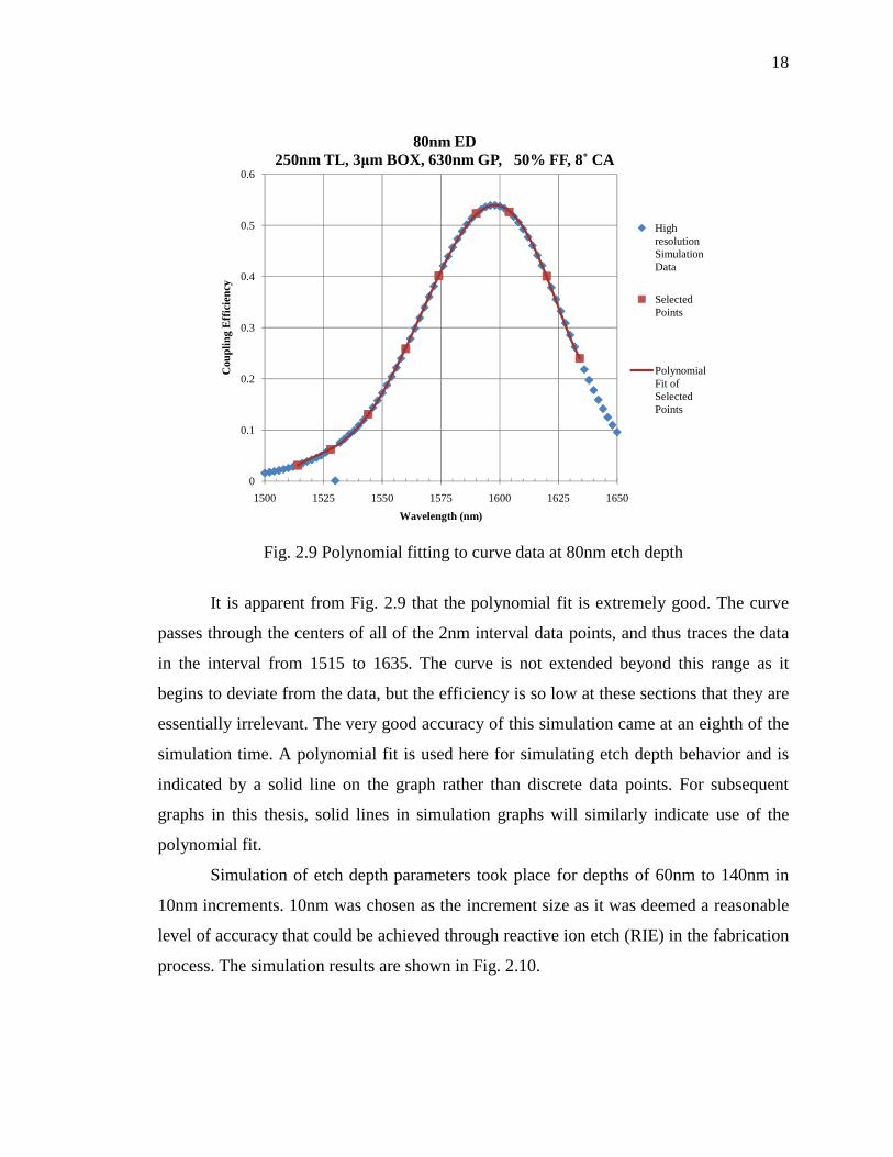
process. The simulation results are shown in Fig. 2.10.
0
0.1
0.2
0.3
0.4
0.5
0.6
1500 1525 1550 1575 1600 1625 1650
Cou
plin
g E
ffic
ienc
y
Wavelength (nm)
80nm ED250nm TL, 3 m BOX, 630nm GP, 50% FF, 8˚ CA
High resolution Simulation Data
Selected Points
Polynomial Fit of Selected Points
19
Fig. 2.10 Comparison of the effects of grating etch depth
It can be seen that etch depth significantly affects center wavelength, bandwidth,
and maximum efficiency. For a 630nm period, the maximum efficiency occurs for an
etch depth of 100nm. However, the maximum for this peak occurs at 1578nm, which is
far above the desired 1550nm target. To achieve maximum coupling at 1550nm, the other
parameters will have to be tweaked in conjunction with the etch depth.
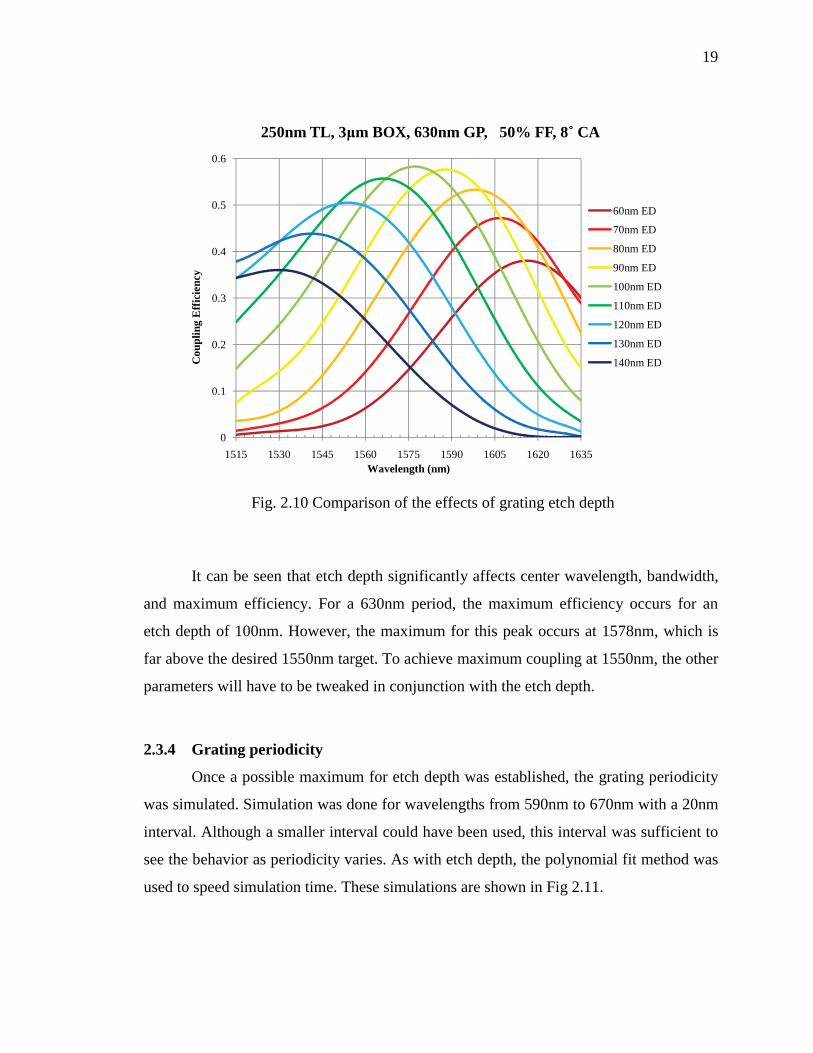
2.3.4 Grating periodicity
Once a possible maximum for etch depth was established, the grating periodicity
was simulated. Simulation was done for wavelengths from 590nm to 670nm with a 20nm
interval. Although a smaller interval could have been used, this interval was sufficient to
see the behavior as periodicity varies. As with etch depth, the polynomial fit method was
used to speed simulation time. These simulations are shown in Fig 2.11.
0
0.1
0.2
0.3
0.4
0.5
0.6
1515 1530 1545 1560 1575 1590 1605 1620 1635
Cou
plin
g E
ffic
ienc
y
Wavelength (nm)
250nm TL, 3 m BOX, 630nm GP, 50% FF, 8˚ CA
60nm ED
70nm ED
80nm ED
90nm ED
100nm ED
110nm ED
120nm ED
130nm ED
140nm ED
20
Fig. 2.11 Comparison of the effects of grating period
As is shown by the plot, the periodicity has a large effect on the coupling
efficiency, as well as the center wavelength and the bandwidth. The maximum efficiency
occurs for 630nm. However, the 610nm period is closer to the center wavelength, has a
higher bandwidth, and has only a slightly smaller coupling efficiency. The 35nm center
wavelength difference between these curves speaks to the large effect the period has on
the curve center.
The effect of the grating period is similar to the effect of etch depth, although the
grating period has a far stronger effect on center wavelength and less on efficiency. The
major difference between the potential real effects of etch depth and grating period is that
the grating period can be very precisely defined using electron beam lithography, while
there is inherent error in defining the grating depth. This means that the grating period
can be known to be very close to the desired value and unchanged by fabrication errors.
0
0.1
0.2
0.3
0.4
0.5
0.6
1515 1530 1545 1560 1575 1590 1605 1620 1635
Cou
plin
g Ef
ficie
ncy
Wavelength (nm)
250nm TL, 3 m BOX, 100nm ED, 50% FF, 8˚ CA
590nm GP
610nm GP
630nm GP
650nm GP
670nm GP
21
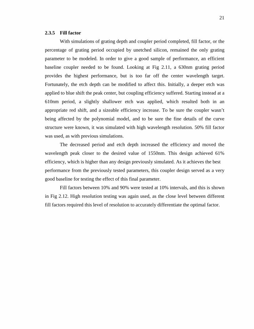
2.3.5 Fill factor
With simulations of grating depth and coupler period completed, fill factor, or the
percentage of grating period occupied by unetched silicon, remained the only grating
parameter to be modeled. In order to give a good sample of performance, an efficient
baseline coupler needed to be found. Looking at Fig 2.11, a 630nm grating period
provides the highest performance, but is too far off the center wavelength target.
Fortunately, the etch depth can be modified to affect this. Initially, a deeper etch was
applied to blue shift the peak center, but coupling efficiency suffered. Starting instead at a
610nm period, a slightly shallower etch was applied, which resulted both in an
appropriate red shift, and a sizeable efficiency increase. To be sure the coupler wasn’t
being affected by the polynomial model, and to be sure the fine details of the curve
structure were known, it was simulated with high wavelength resolution. 50% fill factor
was used, as with previous simulations.
The decreased period and etch depth increased the efficiency and moved the
wavelength peak closer to the desired value of 1550nm. This design achieved 61%
efficiency, which is higher than any design previously simulated. As it achieves the best
performance from the previously tested parameters, this coupler design served as a very
good baseline for testing the effect of this final parameter.
Fill factors between 10% and 90% were tested at 10% intervals, and this is shown
in Fig 2.12. High resolution testing was again used, as the close level between different
fill factors required this level of resolution to accurately differentiate the optimal factor.
22
Fig. 2.12 Comparison of the effects of fill factor
Unlike the previous parameters, fill factor strongly affects the center wavelength
while only weakly the maximum efficiency and bandwidth. Indeed, for factors between
30-70%, the curves are almost identical wavelength shifted copies of each other. Outside
of this range, the grating behavior begins to break down, and efficiency and bandwidth
suffer. The best curve center was obtained using a 50% fill factor.
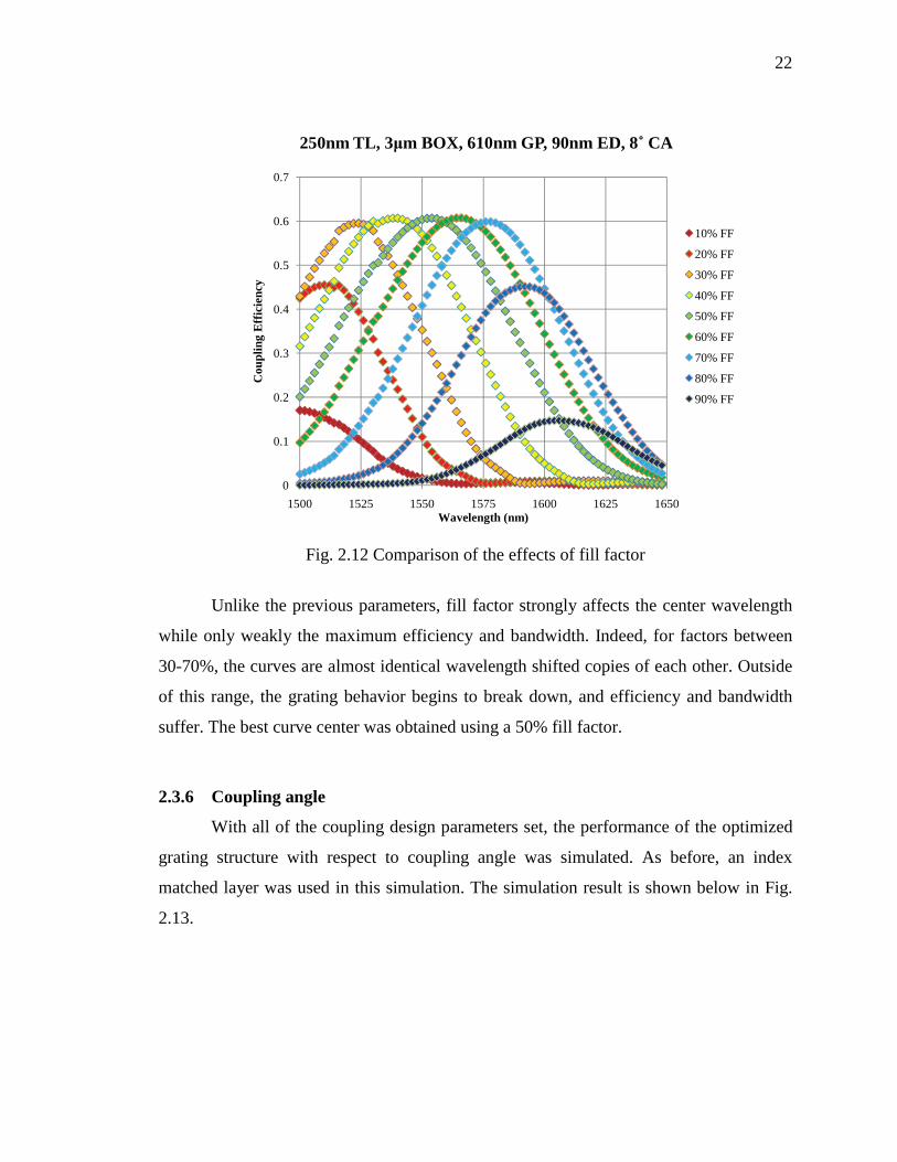
2.3.6 Coupling angle
With all of the coupling design parameters set, the performance of the optimized
grating structure with respect to coupling angle was simulated. As before, an index
matched layer was used in this simulation. The simulation result is shown below in Fig.
2.13.
0
0.1
0.2
0.3
0.4
0.5
0.6
0.7
1500 1525 1550 1575 1600 1625 1650
Cou
plin
g E
ffic
ienc
y
Wavelength (nm)
250nm TL, 3 m BOX, 610nm GP, 90nm ED, 8˚ CA
10% FF
20% FF
30% FF
40% FF
50% FF
60% FF
70% FF
80% FF
90% FF
23
Fig. 2.13 Effect of coupling angle
The effect of the coupling angle is very similar to that of fill factor. Changing the
angle results in changing the center wavelength, but does not affect coupling efficiency or
bandwidth. Therefore, an angle can be chosen that represents a good estimate for
coupling at 1550nm, and further refinement can be had by adjusting the fill factor. Or, if
fabrication error causes the center wavelength to be outside of the acceptable bound, a
different coupling angle could be used to bring it back within range.
2.3.7 Summary of parameter effects
As compared with the reference coupler design from [24], the increased buried
oxide layer results in a 16% efficiency increase and a significant red shift. On its own, the
thicker 250nm silicon top layer increases peak efficiency by 5.5%. The etch depth and
grating periodicity must be optimized for the specific value of the buried oxide layer and
the silicon top layer to achieve maximum efficiency and bandwidth. Fill factor and
coupling angle have little effect on peak efficiency as long as extreme values are not
0
0.1
0.2
0.3
0.4
0.5
0.6
0.7
1500 1510 1520 1530 1540 1550 1560 1570 1580 1590
Cou
plin
g E
ffic
ienc
y
Wavelength (nm)
7.4˚ CA
8.8˚ CA
10.3˚ CA
11.8˚ CA
13.3˚ CA
250nm TL, 3 m BOX, 610nm GP, 90nm ED, 50% FF

24
used. In terms of wavelength effects, all parameter values cause a peak center shift
depending on the value used.
The wavelength shift for groove depth, grating period, and fill factor are all
quadratic with very low parabolic curvature. Since the pertinent wavelength region is
relatively narrow, these can be very effectively approximated as linear functions.
Coupling angle is already entirely linear, so it does not need to be linearized. The linear
effect of changing a given parameter on the wavelength peak is summarized in table 2.1,
along with the correlation coefficient of the parameter’s linear fit. Note that positive shift
values indicate a red shift when increasing the given parameter, and negative values
indicate a blue shift.
Table 2.1 Summary of center wavelength effects of grating parameters
Grating Parameter CW Shift Correlation Coefficient (R) Groove Depth -1.0917nm/nm 0.9984 Grating Period 1.52nm/nm 0.9977
Fill Factor 1.335nm/% 0.9989 Coupling Angle -11.917nm/˚ 0.9998
2.4 Optimized Grating Design
From the simulation in section 2.3, the optimal grating design for a 250nm silicon
top layer and 3 m buried oxide layer wafer was a 610nm grating period, 90nm etch
depth, and 50% fill factor designed to work at a coupling angle of 8˚. This design is
shown in Fig. 2.14.
Fig. 2.14 Optimized grating profile design
Si
3 m
610nm
90nm
305nm160nm 305nm
2SiO
250nm
25
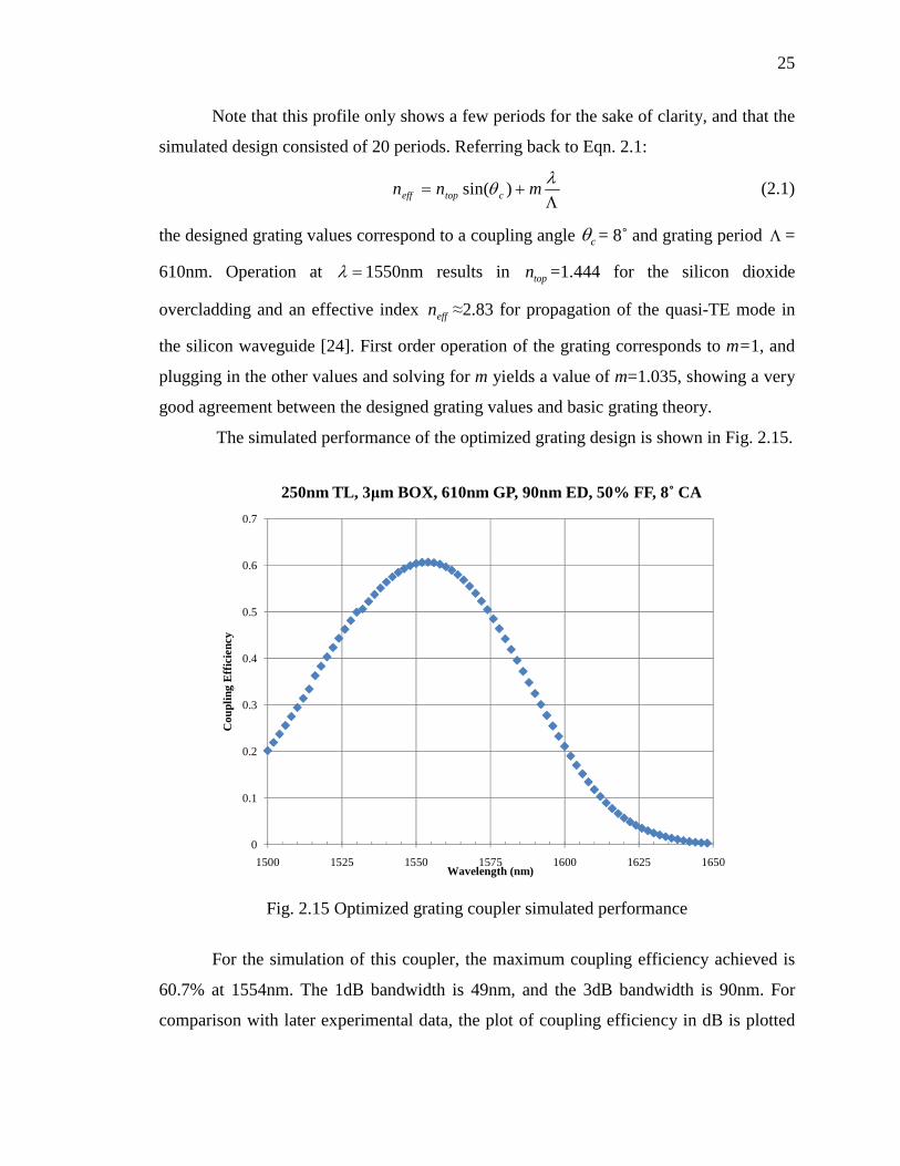
Note that this profile only shows a few periods for the sake of clarity, and that the
simulated design consisted of 20 periods. Referring back to Eqn. 2.1:
mnn ctopeff )sin( (2.1)
the designed grating values correspond to a coupling angle c = 8˚ and grating period =
610nm. Operation at 1550nm results in topn =1.444 for the silicon dioxide
overcladding and an effective index effn 2.83 for propagation of the quasi-TE mode in
the silicon waveguide [24]. First order operation of the grating corresponds to m=1, and
plugging in the other values and solving for m yields a value of m=1.035, showing a very
good agreement between the designed grating values and basic grating theory.
The simulated performance of the optimized grating design is shown in Fig. 2.15.
Fig. 2.15 Optimized grating coupler simulated performance
For the simulation of this coupler, the maximum coupling efficiency achieved is
60.7% at 1554nm. The 1dB bandwidth is 49nm, and the 3dB bandwidth is 90nm. For
comparison with later experimental data, the plot of coupling efficiency in dB is plotted
0
0.1
0.2
0.3
0.4
0.5
0.6
0.7
1500 1525 1550 1575 1600 1625 1650
Cou
plin
g E
ffic
ienc
y
Wavelength (nm)
250nm TL, 3 m BOX, 610nm GP, 90nm ED, 50% FF, 8˚ CA

26
in Fig. 2.16. This is done for fiber-to-fiber loss, and therefore is the combination of loss
from an input and an output coupler. This plot assumes a short waveguide, and thus loss
in the waveguide is negligible. Additionally, any taper loss is neglected. The wavelength
range is reduced slightly to focus on the C-band. Lines at the -1dB and -3dB levels are
plotted for easy graphical identification of the bandwidths.
Fig. 2.16 Optimized grating coupler simulated fiber-to-fiber loss
The maximum efficiency here is -4.4dB. As a result of two couplers being
used, the bandwidth has decreased to 34nm at 1dB, and 59dB at 3dB. From the fit
between experiment and simulation in [24], it can be predicted that experimental
bandwidth will be similar to that shown here, and assuming a similar 45% decrease in
coupling efficiency per coupler, that a -9.5dB fiber to fiber loss could be achieved.
Moving forward, this is the baseline with which to compare experimental data with the
simulated data.
-15
-14
-13
-12
-11
-10
-9
-8
-7
-6
-5
-4
-3
-2
-1
01500 1510 1520 1530 1540 1550 1560 1570 1580 1590 1600
Fibe
r-to
-Fib
er c
oupl
ing
effic
ienc
y (d
B)
Wavelength (nm)
250nm TL, 3 m BOX, 610nm GP, 90nm ED, 50% FF, 8˚ CA
-1dB Line
-3dB Line
27
3. EXPERIMENTAL DESIGN
3.1 In-Coupling and Out-Coupling
3.1.1 Fiber v-groove array
Use of the vertical grating coupler requires at least two optical fibers: one for
input, and one for output. This can be accomplished with the use of two stages, and two
angling setups to hold the fiber at the proper coupling angle. However, stages for use
with alignment so precise are quite expensive, and the use of two stages increases the cost
of a grating coupler system significantly. Using a stage for each input/output (I/O) fiber
also practically limits the system to 2 I/O fibers, as the mechanics involved make adding
more stages difficult, and requires much more chip area. The absolute limit of such a
system is 4 stages and 4 I/O fibers. Furthermore, the use of multiple stages requires
alignment of each stage to be able to do a measurement, which is needlessly tedious.
A better option for vertical coupling is the use of a fiber v-groove assembly [31].
This is an array of optical fibers sandwiched been two small slabs of material, such as
Pyrex or silicon. The end facet of the v-groove can be precisely polished to a desired
angle, which allows for control of the coupling angle. Having multiple fibers in one
device makes possible the use of a single stage for coupling which results in a significant
cost savings. Each v-groove is more than an order of magnitude less expensive than the
cost of an additional stage would be. Furthermore, it allows the use of as many as 32
fibers at once, which makes multiple input/output setups easy to implement. A single
stage is used to align this multitude of fibers, which makes alignment relatively quick and
easy.
Two different v-groove arrays were used for experimentation. The first had a
Pyrex top and a silicon bottom, was polished at 8˚, and had 8 fibers in the array. The
second was an all Pyrex model. It was ordered at a 10˚ angle so as to serve as a

28
comparison to the 8˚ results, and because at 10˚ reflection from fiber to air is slightly
reduced. This Pyrex assembly had 4 fibers in the array. A scale perspective diagram of
this array is shown in Fig 3.1. Note that for the sake of clarity, optical fibers are
highlighted blue.
Fig. 3.1 Scale perspective illustration of Pyrex v-groove array
The fibers are held in place through the use of v-groove channels in the lower
Pyrex section. When ordering the v-groove, these channels were selected to be 250 m
apart. This distance allows for high integration density, while still allowing enough room
for useful structures to be placed in the waveguide section between the couplers. A scale
end facet diagram illustrating this spacing is shown in Fig. 3.2.
Optical Fibers
5.3mm9.56mm
2.5mm
2.5mm
10˚ facet polish
29
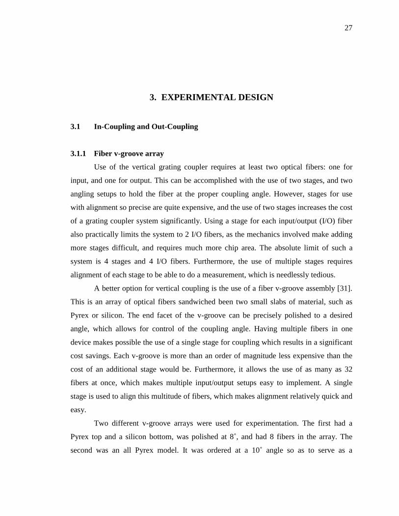
Fig. 3.2 Scale end facet diagram of Pyrex v-groove array
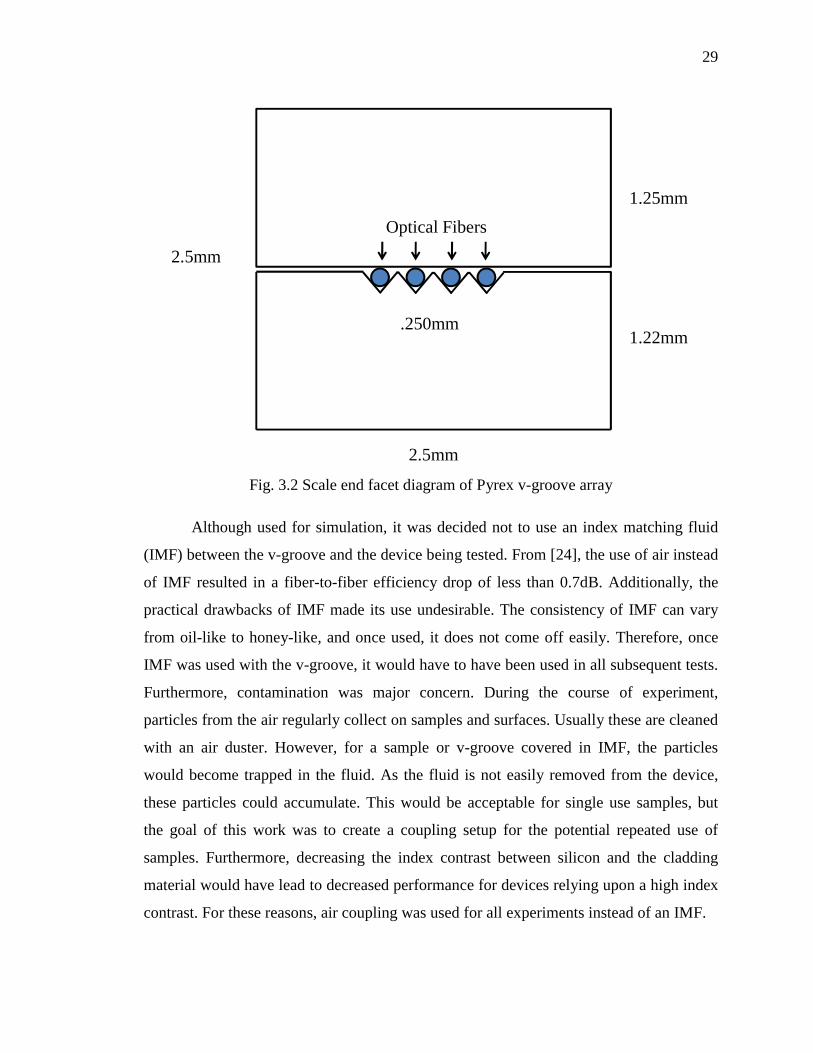
Although used for simulation, it was decided not to use an index matching fluid
(IMF) between the v-groove and the device being tested. From [24], the use of air instead
of IMF resulted in a fiber-to-fiber efficiency drop of less than 0.7dB. Additionally, the
practical drawbacks of IMF made its use undesirable. The consistency of IMF can vary
from oil-like to honey-like, and once used, it does not come off easily. Therefore, once
IMF was used with the v-groove, it would have to have been used in all subsequent tests.
Furthermore, contamination was major concern. During the course of experiment,
particles from the air regularly collect on samples and surfaces. Usually these are cleaned
with an air duster. However, for a sample or v-groove covered in IMF, the particles
would become trapped in the fluid. As the fluid is not easily removed from the device,
these particles could accumulate. This would be acceptable for single use samples, but
the goal of this work was to create a coupling setup for the potential repeated use of
samples. Furthermore, decreasing the index contrast between silicon and the cladding
material would have lead to decreased performance for devices relying upon a high index
contrast. For these reasons, air coupling was used for all experiments instead of an IMF.
Optical Fibers
2.5mm
2.5mm
1.25mm
1.22mm.250mm
30
3.1.2 Precision stage and Imaging
The major hurdle that a fiber array system must overcome, compared to single
fiber coupling, is keeping the entire v-groove end facet flush with the device being tested.
Because the fibers are mounted on the interior of the Pyrex, any angular deviation will
cause one of the Pyrex edges to contact the chip before close coupling is achieved from
the fiber. Pyrex-to-chip contact must be carefully avoided. At the very least, it will result
in decreased performance. At worst, it will damage the chip, the v-groove, or both.
Avoiding this type of contact can be accomplished by using the fiber array with a high
precision positioning stage and a versatile microscope imaging system. The positioning
stage allows accurate angular and translational control of the v-groove, and the imaging
system makes it possible to verify and adjust for proper alignment.
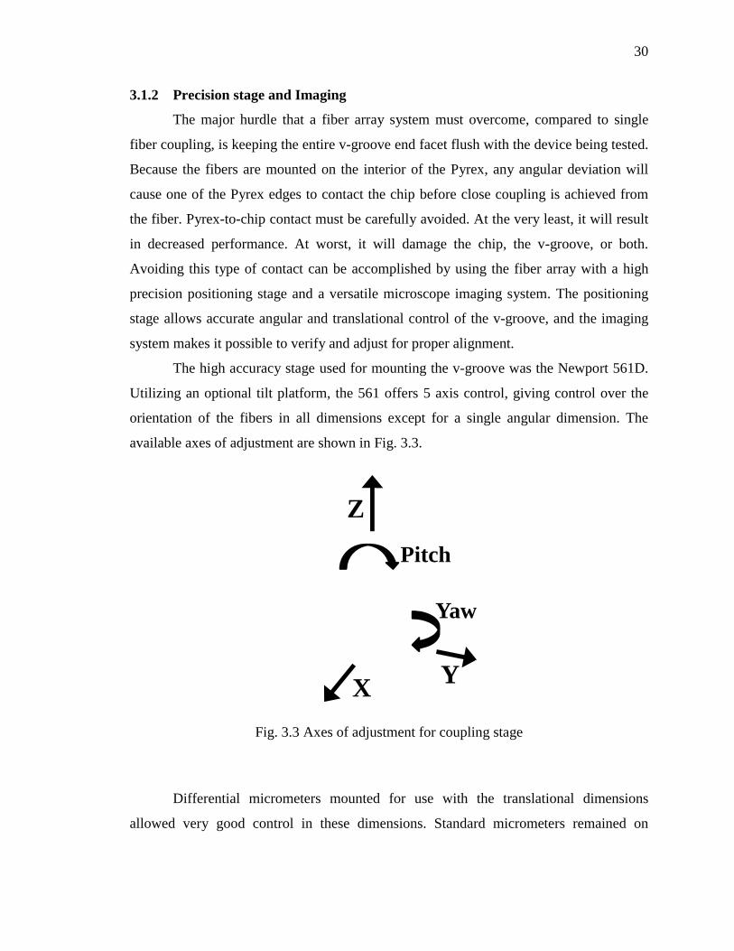
The high accuracy stage used for mounting the v-groove was the Newport 561D.
Utilizing an optional tilt platform, the 561 offers 5 axis control, giving control over the
orientation of the fibers in all dimensions except for a single angular dimension. The
available axes of adjustment are shown in Fig. 3.3.
Fig. 3.3 Axes of adjustment for coupling stage
Differential micrometers mounted for use with the translational dimensions
allowed very good control in these dimensions. Standard micrometers remained on
Z
X Y
Yaw
Pitch
31
angular adjustments, but the already fine level of control was more than enough for
accurate alignment. Note that for the 6th degree of adjustment, roll, is not available on this
stage without an additional attachment.
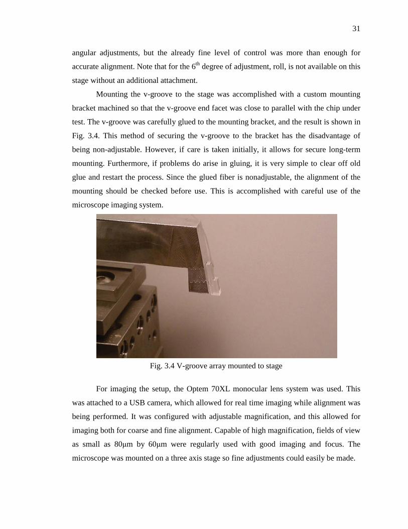
Mounting the v-groove to the stage was accomplished with a custom mounting
bracket machined so that the v-groove end facet was close to parallel with the chip under
test. The v-groove was carefully glued to the mounting bracket, and the result is shown in
Fig. 3.4. This method of securing the v-groove to the bracket has the disadvantage of
being non-adjustable. However, if care is taken initially, it allows for secure long-term
mounting. Furthermore, if problems do arise in gluing, it is very simple to clear off old
glue and restart the process. Since the glued fiber is nonadjustable, the alignment of the
mounting should be checked before use. This is accomplished with careful use of the
microscope imaging system.
Fig. 3.4 V-groove array mounted to stage
For imaging the setup, the Optem 70XL monocular lens system was used. This
was attached to a USB camera, which allowed for real time imaging while alignment was
being performed. It was configured with adjustable magnification, and this allowed for
imaging both for coarse and fine alignment. Capable of high magnification, fields of view
as small as 80 m by 60 m were regularly used with good imaging and focus. The
microscope was mounted on a three axis stage so fine adjustments could easily be made.
32
This imaging system mount was designed such that three different views of the v-
groove and chip could be used. The first is a top down image, or Z view, which was used
for lateral alignment of the chip and imagine of chip features. As this makes up the
majority of the use for the system, and gives the best view of the chip, this was the main
mode of operation for the camera. The second view is a side view of the coupler or X
view. Such a view allows for checking the pitch of the v-groove relative to the wafer,
which could be adjusted as needed. The third view, or a Y view, is straight on to the front
of the coupler. This view allowed for checking the roll accuracy of the glued v-groove.
Additionally, this view allowed for seeing the height of the v-groove off of the chip. This
made it possible to precisely achieve a small coupling gap without chip contact.
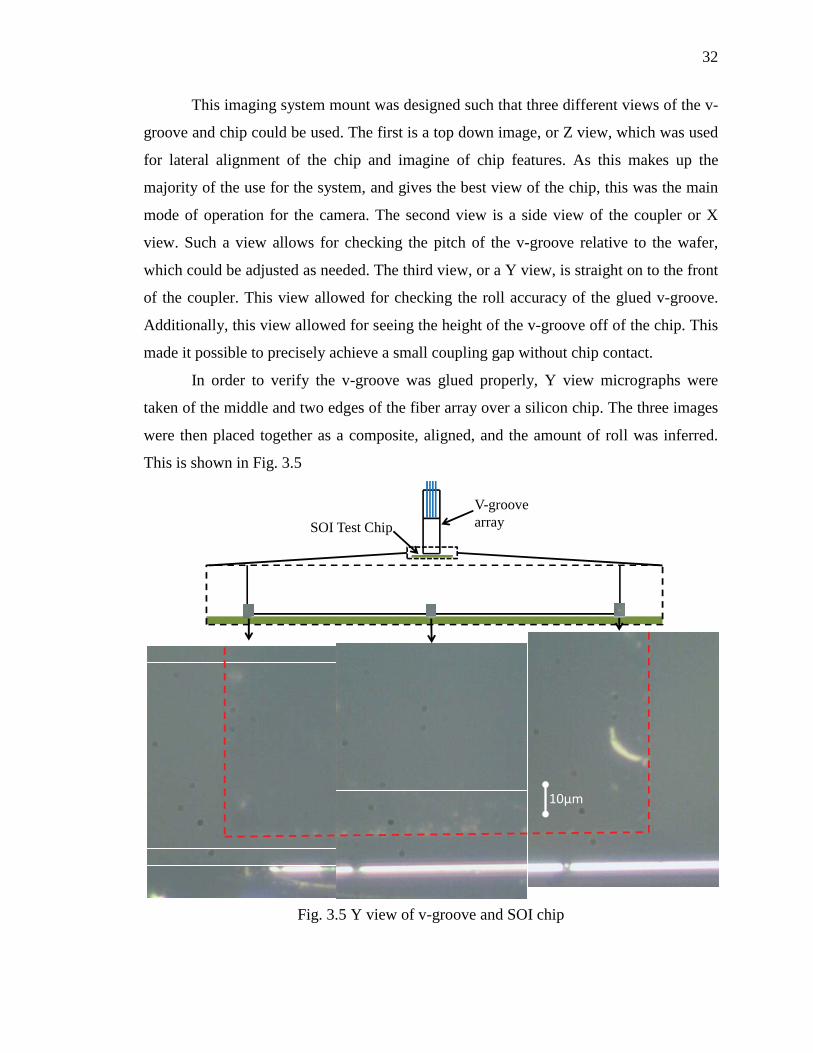
In order to verify the v-groove was glued properly, Y view micrographs were
taken of the middle and two edges of the fiber array over a silicon chip. The three images
were then placed together as a composite, aligned, and the amount of roll was inferred.
This is shown in Fig. 3.5
Fig. 3.5 Y view of v-groove and SOI chip
V-groove arraySOI Test Chip
33
The top illustration shows where the micrograph was taken on the v-groove. The
micrographs are somewhat poorly defined due to the fact that the fiber array is angled
away from the camera in this view. As a result, most of the light projected by the
microscope system gets reflected away from the camera as well. As is shown in the
figure, the amount of roll variation over the entire width of the v-groove is less than 1 m.
Therefore, gluing the fiber was able to be a very accurate method of alignment.
Similarly, a set of X view micrographs were taken to check the alignment of
pitch. This angle is adjustable, and was optimized before the micrographs were taken.
They are shown in Fig. 3.6.
Fig. 3.6 X view of v-groove and SOI chip
As before, the top illustration shows where each micrographs was taken on the
side of the v-groove. Note that the gap in the center image is not a fiber, but is the
separation between the two Pyrex slabs. This figure shows that pitch alignment is very
V-groove arraySOI Test Chip
34
good as well. Displacement from the back of the array to the middle section is less than
1 m. The front section, however, is slightly higher than the rest of the array. This is due
to an actual sloping of the front edge of the v-groove, and not due to angular
misalignment. Since this sloping is away from the chip and not towards it, it does not
harm alignment, and is not an issue.
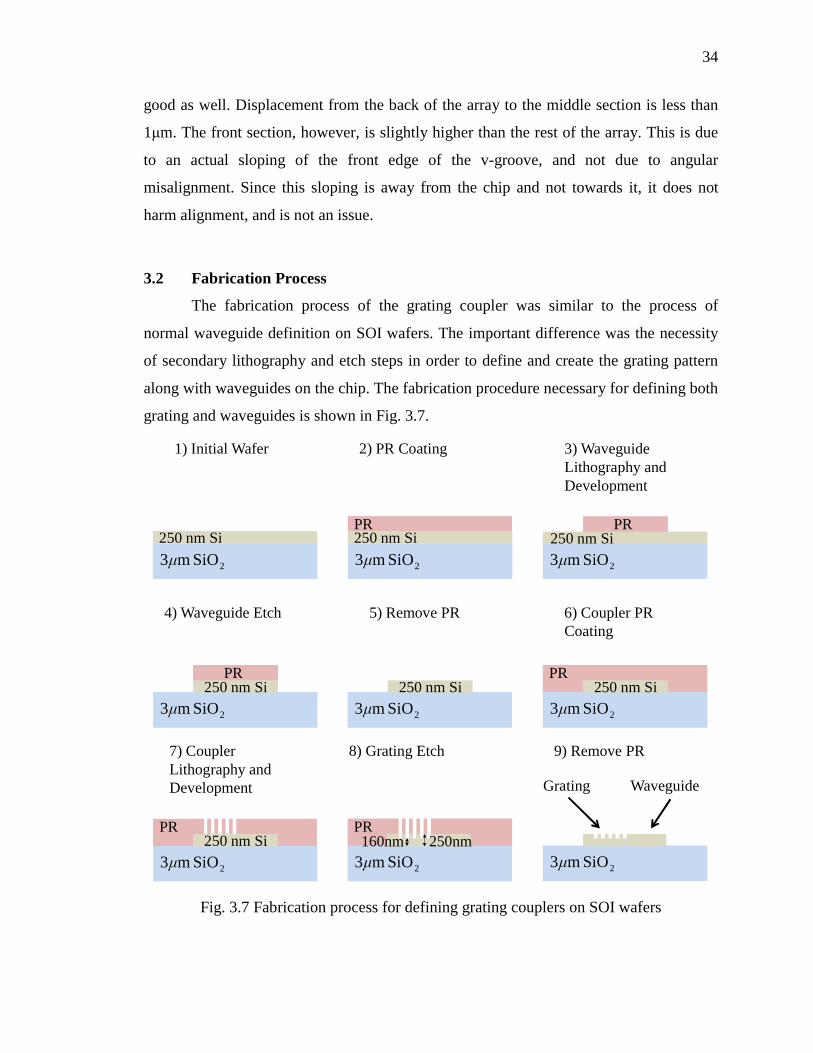
3.2 Fabrication Process
The fabrication process of the grating coupler was similar to the process of
normal waveguide definition on SOI wafers. The important difference was the necessity
of secondary lithography and etch steps in order to define and create the grating pattern
along with waveguides on the chip. The fabrication procedure necessary for defining both
grating and waveguides is shown in Fig. 3.7.
Fig. 3.7 Fabrication process for defining grating couplers on SOI wafers
1) Initial Wafer 2) PR Coating
7) Coupler Lithography and Development
8) Grating Etch 9) Remove PR
3) Waveguide Lithography and Development
4) Waveguide Etch 5) Remove PR 6) Coupler PR Coating
250 nm SiPR
2SiOm3250 nm Si
2SiOm3
2SiOm3
250nm
Grating Waveguide
PR
2SiOm3250 nm Si
PR
2SiOm3250 nm Si
2SiOm3250 nm Si
PR
2SiOm3250 nm Si
PR
2SiOm3250 nm Si
PR
2SiOm3160nm 250nm
35
Steps 1 to 5 describe the normal process for defining waveguides. Step 1 shows
the unprocessed wafer, and step 2 consists of a negative photoresist spin coating.
Negative resist is used because it is significantly more efficient to expose the area that
will make up the waveguide instead of having to expose the empty space on the chip or
having to define trenches. Step 3 is the use of electron beam lithography to define the
waveguide areas. It first involves exposing the photoresist with the electron beam to
polymerize the photoresist over the waveguide area. Then, the chip is put into a developer
to remove all the unexposed photoresist. Step 4 is etching away the exposed areas of
exposed silicon top layer using reactive ion etch (RIE). Removal of the remaining
photoresist is step 5. At the conclusion of this step, the waveguides and grating pads have
been fully defined.
Steps 6 to 9 are the additional steps required to make the grating pattern. The chip
is recoated in photoresist in step 6. Step 7 consists of lithography and development
similar to step 3, except the electron beam is exposing only the grating pattern. Step 8 is
RIE etching of the silicon top layer to define the trenches in the grating pattern. And
finally, step 9 is the removal of the remaining photoresist. The grating couplers, along
with the waveguide sections, are thus defined after this step.
3.3 Coupler Layout
Both straight and curved types of couplers were to be used for initial testing and
layouts were required for each. For the straight coupler, an area of 10 m by 11.6 m,
incorporating 19 grating periods, was used. A scale illustration of the structure is shown
in Fig. 3.8.
36
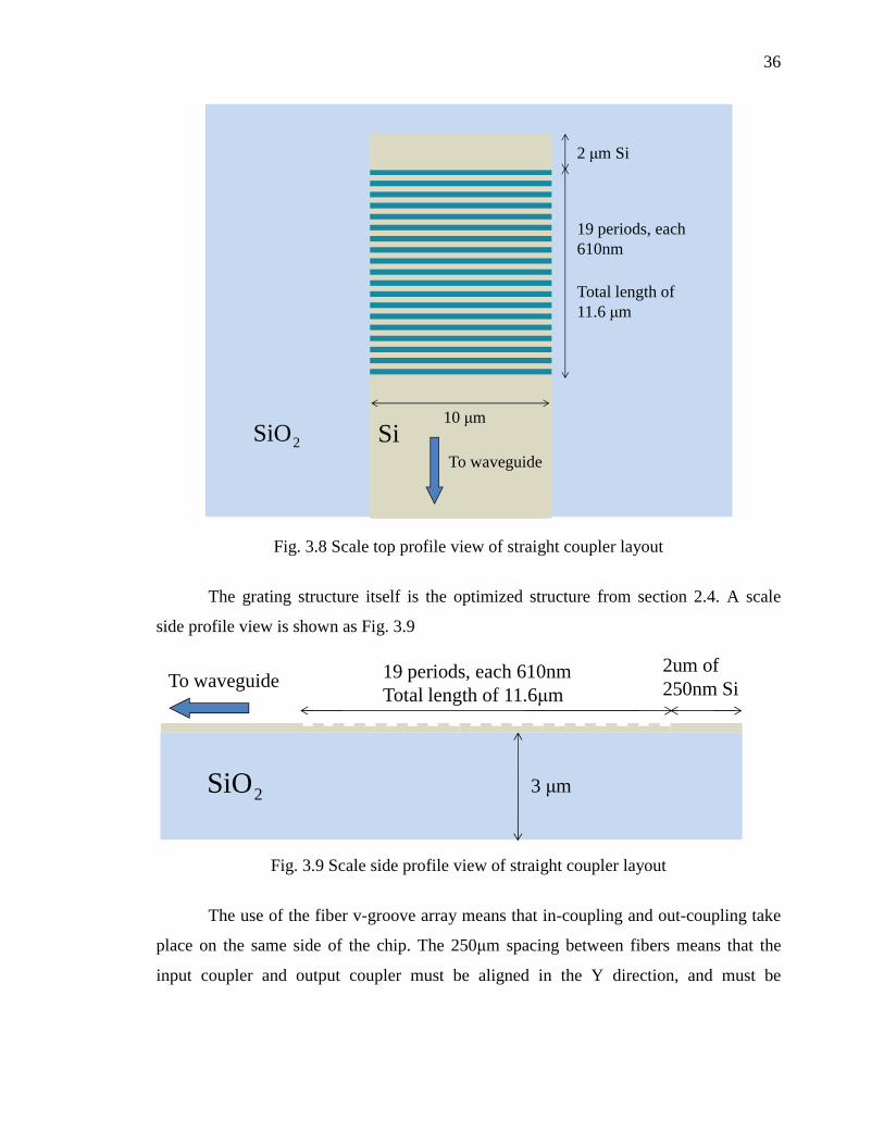
Fig. 3.8 Scale top profile view of straight coupler layout
The grating structure itself is the optimized structure from section 2.4. A scale
side profile view is shown as Fig. 3.9
Fig. 3.9 Scale side profile view of straight coupler layout
The use of the fiber v-groove array means that in-coupling and out-coupling take
place on the same side of the chip. The 250 m spacing between fibers means that the
input coupler and output coupler must be aligned in the Y direction, and must be
19 periods, each 610nm
Si
2 m Si
10 m2SiO
To waveguide
Total length of 11.6 m
3 m
To waveguide2um of 250nm Si
2SiO
19 periods, each 610nmTotal length of 11.6 m

37
separated by multiples of 250 m in the X direction. This is accomplished by curving the
waveguide section. Distance between couplers in this layout is 250 m. The straight
coupling layout is shown in Fig. 3.10.
Fig. 3.10 Layout of straight coupling setup (Layout and figure courtesy of Li Fan)
The grating is connected to the silicon waveguide with a parabolic taper. The
taper is short (40 m) to test how coupling of the straight coupler compares to a focused
coupler when the two are of a similar footprint. Here (and similarly, but with different
dimensions, for the parabolic tapers in chapter 5) the taper is defined as a parabola
passing through the edges of the 500nm wide waveguide section and also through the
edges of the 10 m wide grating a distance 40 m away. The silicon waveguide after the
taper is curved at a radius that should not add any appreciable loss to the system. A 10 m
diameter ring resonator, set at a coupling distance of 200nm, is added in between the
couplers to a feature to the coupler wavelength spectrum.
The curved coupler layout was based on the reference curved design [27] and was
designed so that the coupler approximates Eqn. 2.3 as concentric circular focusing
elements. As it is focused, no taper is needed. The focal distance, or the distance from the
start of the waveguide to the start of the grating, is 22 m. The layout is shown below in
Fig. 3.11
10 m

38
Fig. 3.11 Layout of curved coupling setup (Layout and figure courtesy of Li Fan)
The distance between the couplers is 250 m as in the straight coupling setup. The
grating region is 11.6 m swept across 44˚. As before, a ring resonator at a coupling
distance of 200nm was used. For the curved couplers, however, a 20 m ring diameter
was used in an effort to help differentiate coupling setups.
With a method for accurate fiber placement, a fabrication process, and layouts for
basic coupling structures, characterization was made possible for fabricated coupling
structures.
10 m
39
4. EXPERIMENTAL CHARACTERIZATION
4.1 Characterization Setup
Bulk optical components were used for the laser source and polarization control.
A fine resolution tunable laser source was used as the infrared source. This was
connected to a fiber polarization controller for selecting the quasi-TE mode when doing
alignment. This polarization controller was rated at 40dB polarization extinction, which
was more than enough for the polarization needs of the coupler. The polarization
controller was then connected to the v-groove, which coupled light into the sample and
back out to the v-groove. This was connected to a fiber power detector.
For all measurements, the power loss was measured from the fiber laser, though
the polarization controller, and into to the power detector. This is the inherent system
loss, and was re-measured and subtracted out of all power measurements. Therefore, the
fiber-to-fiber loss displayed is the loss into the v-groove, thought the grating couplers on
chip, and back into and out of the v-groove. Since the fiber connector loss from the v-
groove is negligible, this effectively measured the loss of only the grating couplers.
4.1.1 Sample inspection
Before testing began, micrographs were taken of the fabricated chip to visually
verify the layout. These micrographs are shown as Fig. 4.1. These, and all devices
mentioned later, were fabricated by Leo Varghese and Li Fan.
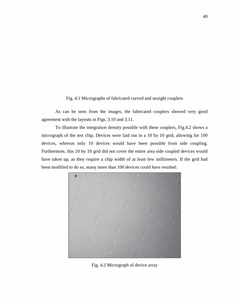
Fig. 4.1 Mic
As can be seen
agreement with the layou
To illustrate the in
micrograph of the test ch
devices, whereas only
Furthermore, this 10 by 1
have taken up, as they r
been modified to do so, m
crographs of fabricated curved and straight coup
from the images, the fabricated couplers sho
uts in Figs. 3.10 and 3.11.
ntegration density possible with these couplers,
hip. Devices were laid out in a 10 by 10 grid,
10 devices would have been possible from
10 grid did not cover the entire area side couple
equire a chip width of at least few millimeters
many more than 100 devices could have resulted
Fig. 4.2 Micrograph of device array
40
plers
owed very good
, Fig.4.2 shows a
allowing for 100
m side coupling.
ed devices would
s. If the grid had
d.
41
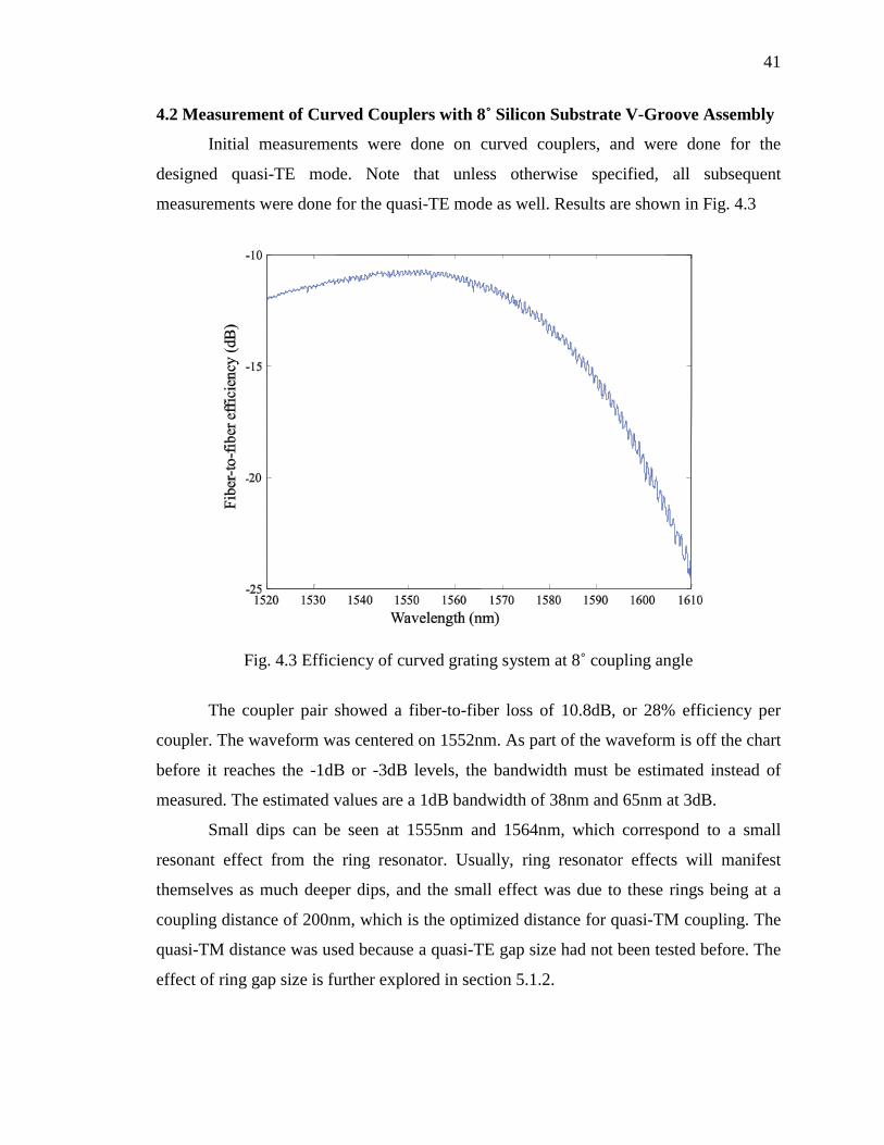
4.2 Measurement of Curved Couplers with 8˚ Silicon Substrate V-Groove Assembly
Initial measurements were done on curved couplers, and were done for the
designed quasi-TE mode. Note that unless otherwise specified, all subsequent
measurements were done for the quasi-TE mode as well. Results are shown in Fig. 4.3
Fig. 4.3 Efficiency of curved grating system at 8˚ coupling angle
The coupler pair showed a fiber-to-fiber loss of 10.8dB, or 28% efficiency per
coupler. The waveform was centered on 1552nm. As part of the waveform is off the chart
before it reaches the -1dB or -3dB levels, the bandwidth must be estimated instead of
measured. The estimated values are a 1dB bandwidth of 38nm and 65nm at 3dB.
Small dips can be seen at 1555nm and 1564nm, which correspond to a small
resonant effect from the ring resonator. Usually, ring resonator effects will manifest
themselves as much deeper dips, and the small effect was due to these rings being at a
coupling distance of 200nm, which is the optimized distance for quasi-TM coupling. The
quasi-TM distance was used because a quasi-TE gap size had not been tested before. The
effect of ring gap size is further explored in section 5.1.2.
42
4.2.1 Fabry-Perot effects
A close up view of part of the spectrum is shown in Fig. 4.4. A definite 0.2dB
peak-to-peak periodic variation in the intensity was present throughout the wavelength
range. This variation was regular, and seems to be the result of a Fabry-Perot resonance
cavity being formed in the waveguide section between the input and output couplers. The
cavity is formed when light travelling from the waveguide to the grating is not diffracted,
but instead reflects off the silicon to air interface at the back end of the grating structure.
The light then continues back through the waveguide. From micrographs of devices and
Fig. 3.11, the cavity length was estimated to be 373 m.
Fig. 4.4 Periodic response of curved grating system
To confirm the effect is indeed a Fabry-Perot variation, predicted Fabry-Perot
cavity length was calculated and compared to the actual cavity length. From Fig. 4.4, the
average free spectral range (FSR) for the peaks from 1547-1554nm was found to be
0.864nm. For the case of normal reflector incidence [32], and for long cavity lengths
compared to the wavelength size, the free spectral range for a cavity is given by:
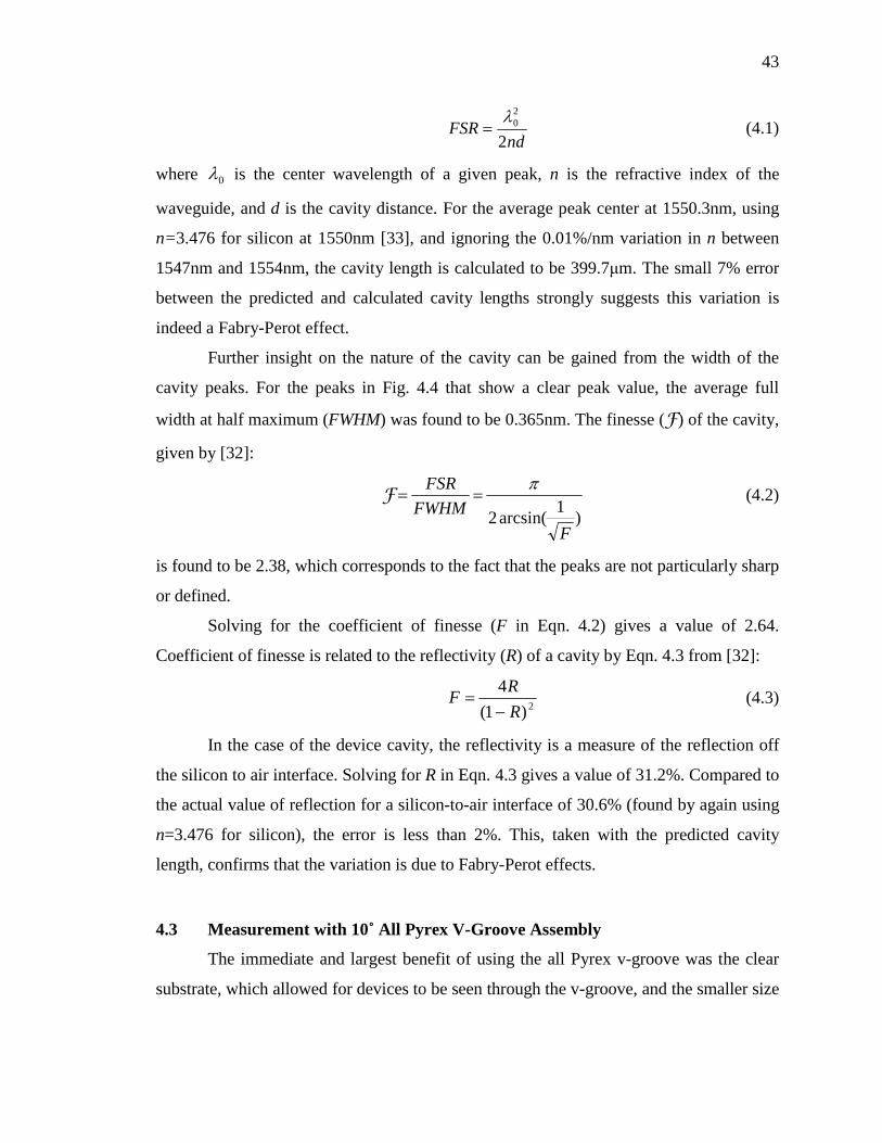
43
ndFSR
2
20 (4.1)
where 0 is the center wavelength of a given peak, n is the refractive index of the
waveguide, and d is the cavity distance. For the average peak center at 1550.3nm, using
n=3.476 for silicon at 1550nm [33], and ignoring the 0.01%/nm variation in n between
1547nm and 1554nm, the cavity length is calculated to be 399.7 m. The small 7% error
between the predicted and calculated cavity lengths strongly suggests this variation is
indeed a Fabry-Perot effect.
Further insight on the nature of the cavity can be gained from the width of the
cavity peaks. For the peaks in Fig. 4.4 that show a clear peak value, the average full
width at half maximum (FWHM) was found to be 0.365nm. The finesse ( ) of the cavity,
given by [32]:
)1arcsin(2F
FWHMFSR (4.2)
is found to be 2.38, which corresponds to the fact that the peaks are not particularly sharp
or defined.
Solving for the coefficient of finesse (F in Eqn. 4.2) gives a value of 2.64.
Coefficient of finesse is related to the reflectivity (R) of a cavity by Eqn. 4.3 from [32]:
2)1(4
RRF (4.3)
In the case of the device cavity, the reflectivity is a measure of the reflection off
the silicon to air interface. Solving for R in Eqn. 4.3 gives a value of 31.2%. Compared to
the actual value of reflection for a silicon-to-air interface of 30.6% (found by again using
n=3.476 for silicon), the error is less than 2%. This, taken with the predicted cavity
length, confirms that the variation is due to Fabry-Perot effects.
4.3 Measurement with 10˚ All Pyrex V-Groove Assembly
The immediate and largest benefit of using the all Pyrex v-groove was the clear
substrate, which allowed for devices to be seen through the v-groove, and the smaller size
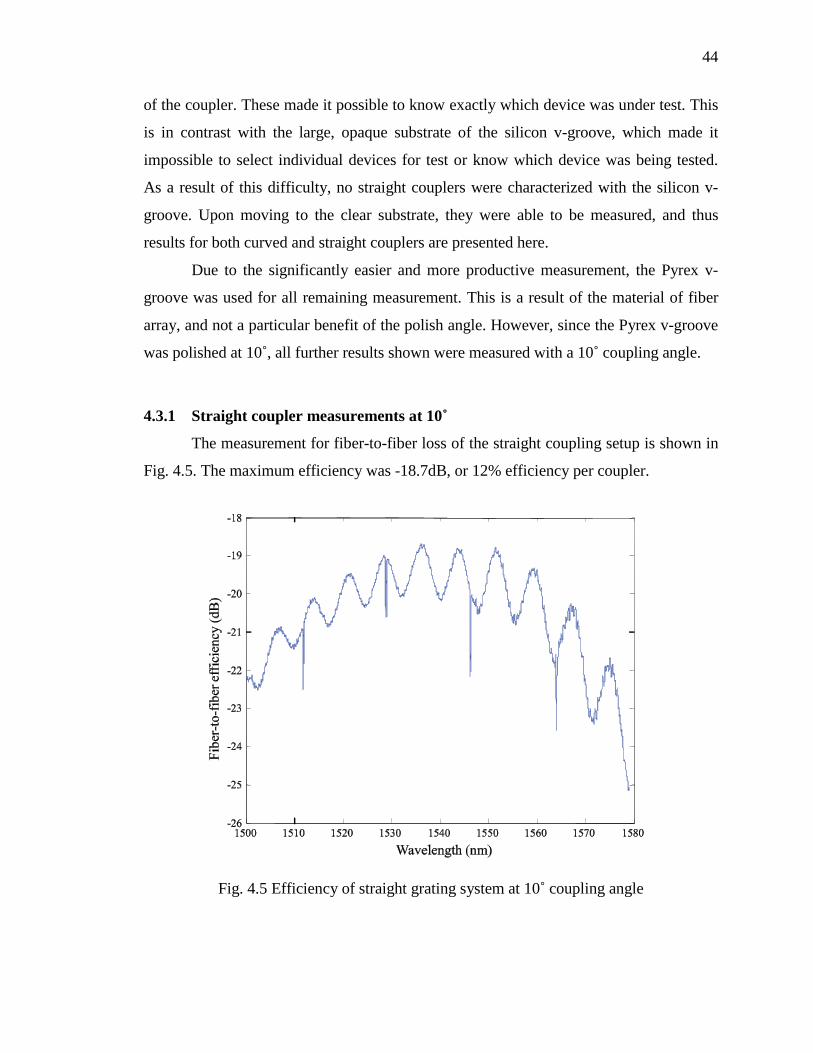
44
of the coupler. These made it possible to know exactly which device was under test. This
is in contrast with the large, opaque substrate of the silicon v-groove, which made it
impossible to select individual devices for test or know which device was being tested.
As a result of this difficulty, no straight couplers were characterized with the silicon v-
groove. Upon moving to the clear substrate, they were able to be measured, and thus
results for both curved and straight couplers are presented here.
Due to the significantly easier and more productive measurement, the Pyrex v-
groove was used for all remaining measurement. This is a result of the material of fiber
array, and not a particular benefit of the polish angle. However, since the Pyrex v-groove
was polished at 10˚, all further results shown were measured with a 10˚ coupling angle.
4.3.1 Straight coupler measurements at 10˚
The measurement for fiber-to-fiber loss of the straight coupling setup is shown in
Fig. 4.5. The maximum efficiency was -18.7dB, or 12% efficiency per coupler.
Fig. 4.5 Efficiency of straight grating system at 10˚ coupling angle
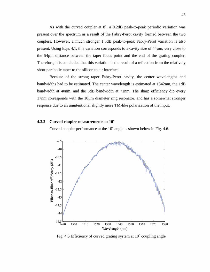
45
As with the curved coupler at 8˚, a 0.2dB peak-to-peak periodic variation was
present over the spectrum as a result of the Fabry-Perot cavity formed between the two
couplers. However, a much stronger 1.5dB peak-to-peak Fabry-Perot variation is also
present. Using Eqn. 4.1, this variation corresponds to a cavity size of 44 m, very close to
the 54 m distance between the taper focus point and the end of the grating coupler.
Therefore, it is concluded that this variation is the result of a reflection from the relatively
short parabolic taper to the silicon to air interface.
Because of the strong taper Fabry-Perot cavity, the center wavelengths and
bandwidths had to be estimated. The center wavelength is estimated at 1542nm, the 1dB
bandwidth at 40nm, and the 3dB bandwidth at 71nm. The sharp efficiency dip every
17nm corresponds with the 10 m diameter ring resonator, and has a somewhat stronger
response due to an unintentional slightly more TM-like polarization of the input.
4.3.2 Curved coupler measurements at 10˚
Curved coupler performance at the 10˚ angle is shown below in Fig. 4.6.
Fig. 4.6 Efficiency of curved grating system at 10˚ coupling angle
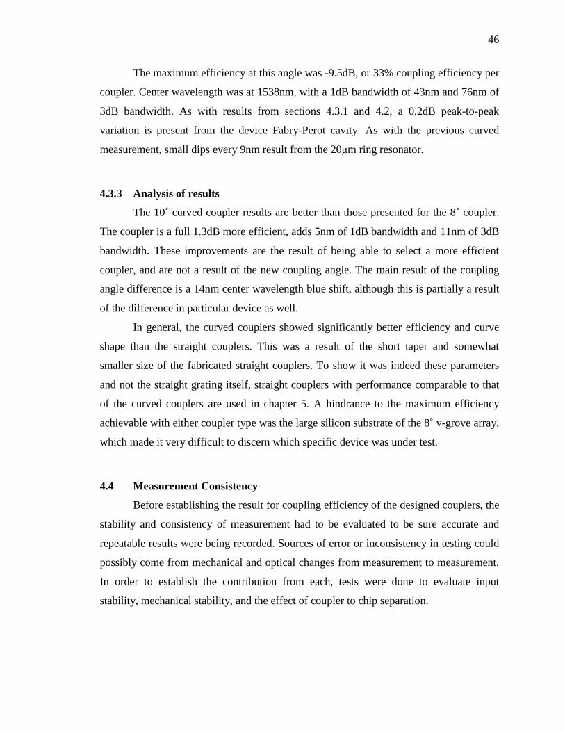
46
The maximum efficiency at this angle was -9.5dB, or 33% coupling efficiency per
coupler. Center wavelength was at 1538nm, with a 1dB bandwidth of 43nm and 76nm of
3dB bandwidth. As with results from sections 4.3.1 and 4.2, a 0.2dB peak-to-peak
variation is present from the device Fabry-Perot cavity. As with the previous curved
measurement, small dips every 9nm result from the 20 m ring resonator.
4.3.3 Analysis of results
The 10˚ curved coupler results are better than those presented for the 8˚ coupler.
The coupler is a full 1.3dB more efficient, adds 5nm of 1dB bandwidth and 11nm of 3dB
bandwidth. These improvements are the result of being able to select a more efficient
coupler, and are not a result of the new coupling angle. The main result of the coupling
angle difference is a 14nm center wavelength blue shift, although this is partially a result
of the difference in particular device as well.
In general, the curved couplers showed significantly better efficiency and curve
shape than the straight couplers. This was a result of the short taper and somewhat
smaller size of the fabricated straight couplers. To show it was indeed these parameters
and not the straight grating itself, straight couplers with performance comparable to that
of the curved couplers are used in chapter 5. A hindrance to the maximum efficiency
achievable with either coupler type was the large silicon substrate of the 8˚ v-grove array,
which made it very difficult to discern which specific device was under test.
4.4 Measurement Consistency
Before establishing the result for coupling efficiency of the designed couplers, the
stability and consistency of measurement had to be evaluated to be sure accurate and
repeatable results were being recorded. Sources of error or inconsistency in testing could
possibly come from mechanical and optical changes from measurement to measurement.
In order to establish the contribution from each, tests were done to evaluate input
stability, mechanical stability, and the effect of coupler to chip separation.

47
4.4.1 Input stability
Input stability was evaluated by aligning the system, then running multiple tests
without disturbing the mechanics or any part of the fiber line. A wavelength scan was run
initially, and then repeated at 8, 12, 20, and 25 minutes after the initial scan. The results
are shown in Fig. 4.7
Fig. 4.7 Effect of coupling efficiency with time
For the undisturbed system, the coupling efficiency did indeed change with time.
Throughout the center of the spectrum, this change was within ±0.25dB, though it
exceeded this at the ends of the spectrum. This efficiency drift is random, and not the
result of some kind of mechanical drift or signal degradation, as the power level both
increased and decreased with time. Relative efficiency levels between the curves changed
throughout the spectrum, and the “most efficient” curve depends entirely on the
wavelength. This means the spectral shape depended upon the time at which the
measurement was taken. However, the spectral shapes of small features were not affected
much at all. This is shown in Fig. 4.8. Regardless of the power level, the fine detail of the
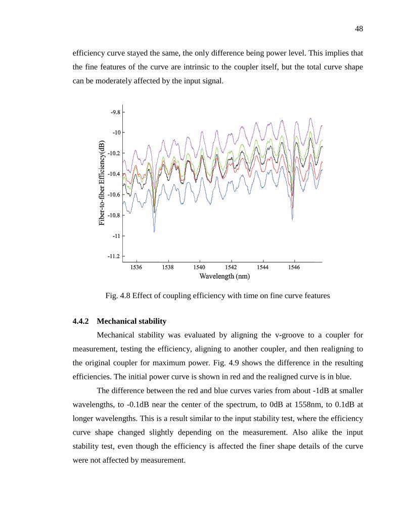
48
efficiency curve stayed the same, the only difference being power level. This implies that
the fine features of the curve are intrinsic to the coupler itself, but the total curve shape
can be moderately affected by the input signal.
Fig. 4.8 Effect of coupling efficiency with time on fine curve features
4.4.2 Mechanical stability
Mechanical stability was evaluated by aligning the v-groove to a coupler for
measurement, testing the efficiency, aligning to another coupler, and then realigning to
the original coupler for maximum power. Fig. 4.9 shows the difference in the resulting
efficiencies. The initial power curve is shown in red and the realigned curve is in blue.
The difference between the red and blue curves varies from about -1dB at smaller
wavelengths, to -0.1dB near the center of the spectrum, to 0dB at 1558nm, to 0.1dB at
longer wavelengths. This is a result similar to the input stability test, where the efficiency
curve shape changed slightly depending on the measurement. Also alike the input
stability test, even though the efficiency is affected the finer shape details of the curve
were not affected by measurement.

49
Fig. 4.9 Effect of mechanical realignment
It is significant that the curves match at 1558nm, as this is the wavelength that
alignment was done at. What likely occurred was that the curves were realigned to
exactly match up at that wavelength, but the rest of the curve behavior had changed due
to input instability. Therefore, it can be said that the mechanical repeatability is very
good, and is bound by the input instability.
4.4.3 Coupler to chip separation
The effect of chip separation was tested using the microscope camera in an X
profile alignment. The distance between the chip and v-groove was measured using what
was known about the scale of the microscope at maximum magnification. Like the
mechanical stability and the system stability, and as a result of changing the separation,
the efficiency curves had slightly different curve shapes but unchanged fine plot features.
A plot showing the peak efficiencies at different heights for a curved coupler is shown in
Fig 4.10.
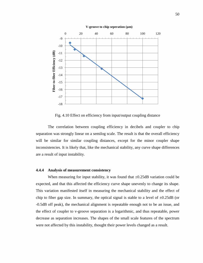
50
Fig. 4.10 Effect on efficiency from input/output coupling distance
The correlation between coupling efficiency in decibels and coupler to chip
separation was strongly linear on a semilog scale. The result is that the overall efficiency
will be similar for similar coupling distances, except for the minor coupler shape
inconsistencies. It is likely that, like the mechanical stability, any curve shape differences
are a result of input instability.
4.4.4 Analysis of measurement consistency
When measuring for input stability, it was found that ±0.25dB variation could be
expected, and that this affected the efficiency curve shape unevenly to change its shape.
This variation manifested itself in measuring the mechanical stability and the effect of
chip to fiber gap size. In summary, the optical signal is stable to a level of ±0.25dB (or
-0.5dB off peak), the mechanical alignment is repeatable enough not to be an issue, and
the effect of coupler to v-groove separation is a logarithmic, and thus repeatable, power
decrease as separation increases. The shapes of the small scale features of the spectrum
were not affected by this instability, thought their power levels changed as a result.
-18
-17
-16
-15
-14
-13
-12
-11
-10
-90 20 40 60 80 100 120
Fibe
r-to
-fib
er E
ffic
ienc
y (d
B)
V-groove to chip seperation ( m)

51
4.5 Device Consistency
As the grating coupler is meant to be used in conjunction with photonic devices, it
needs to be able to perform consistently in the devices it is used with. In order to test this
consistency, a random row of devices on the chip was selected and tested. The fine
structure results are shown in Fig. 4.11, and the efficiency spectrum results are shown in
Fig. 4.12.
Fig. 4.11 Fine structure comparison of 5 different devices
For measures of single device stability, as shown in Fig 4.7, the fine structure of
the spectrum does not change. However, when looking at different couplers, the fine
structure differs noticeably from device to device. This could potentially allow for
determining whether a set of wavelength scans comes from the same or different devices.
The possible application of this is explored in the “Future Work” section of chapter 6.
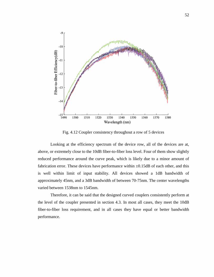
52
Fig. 4.12 Coupler consistency throughout a row of 5 devices
Looking at the efficiency spectrum of the device row, all of the devices are at,
above, or extremely close to the 10dB fiber-to-fiber loss level. Four of them show slightly
reduced performance around the curve peak, which is likely due to a minor amount of
fabrication error. These devices have performance within ±0.15dB of each other, and this
is well within limit of input stability. All devices showed a 1dB bandwidth of
approximately 45nm, and a 3dB bandwidth of between 70-75nm. The center wavelengths
varied between 1538nm to 1545nm.
Therefore, it can be said that the designed curved couplers consistently perform at
the level of the coupler presented in section 4.3. In most all cases, they meet the 10dB
fiber-to-fiber loss requirement, and in all cases they have equal or better bandwidth
performance.
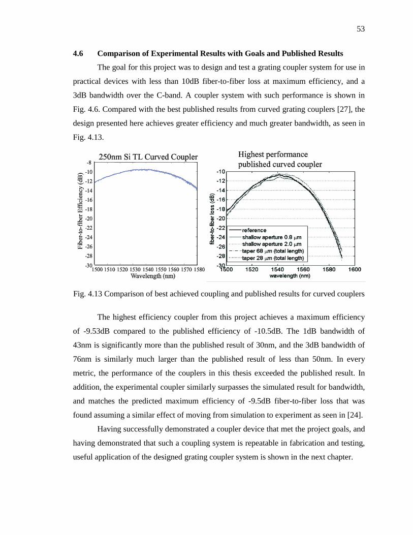
53
4.6 Comparison of Experimental Results with Goals and Published Results
The goal for this project was to design and test a grating coupler system for use in
practical devices with less than 10dB fiber-to-fiber loss at maximum efficiency, and a
3dB bandwidth over the C-band. A coupler system with such performance is shown in
Fig. 4.6. Compared with the best published results from curved grating couplers [27], the
design presented here achieves greater efficiency and much greater bandwidth, as seen in
Fig. 4.13.
Fig. 4.13 Comparison of best achieved coupling and published results for curved couplers
The highest efficiency coupler from this project achieves a maximum efficiency
of -9.53dB compared to the published efficiency of -10.5dB. The 1dB bandwidth of
43nm is significantly more than the published result of 30nm, and the 3dB bandwidth of
76nm is similarly much larger than the published result of less than 50nm. In every
metric, the performance of the couplers in this thesis exceeded the published result. In
addition, the experimental coupler similarly surpasses the simulated result for bandwidth,
and matches the predicted maximum efficiency of -9.5dB fiber-to-fiber loss that was
found assuming a similar effect of moving from simulation to experiment as seen in [24].
Having successfully demonstrated a coupler device that met the project goals, and
having demonstrated that such a coupling system is repeatable in fabrication and testing,
useful application of the designed grating coupler system is shown in the next chapter.
54
5. PRACTICAL APPLICATION
In an effort to expand the versatility of the grating coupler, as well as the devices
used with it, silicon devices were fabricated using an amorphous silicon top layer instead
of the single crystal silicon used previously. A benefit of amorphous silicon is that
devices are not restricted to a single top layer thickness. Additionally, it becomes possible
to deposit the buried oxide layer instead of being constrained by the thickness in a
purchased wafer. As a result, much greater freedom is possible with respect to device
structure.
Furthermore, used in conjunction with low temperature fabrication techniques, it
could be possible to use a flexible polymer substrate instead of a crystalline silicon one.
This would result in a flexible nanophotonic device. The fiber v-groove array, if used
with index matching glue, could provide a permanent method of attaching input and
output capabilities to such a device.
Two amorphous silicon devices are presented here. The first is a three-port device
that makes use of ring resonators for power coupling between waveguides. As ring
resonators are very often used in nanophotonic devices, their successful demonstration is
important for showing the grating couplers designed in chapter 4 can be used in practical
devices. The second device is a one dimensional photonic crystal cavity, similar to [34].
This is a device that needed the short waveguide length allowed by grating couplers to
function. The results shown here for the device are preliminary. However, they
demonstrate the use of the designed grating couplers in an actual device, thus fulfilling
the project goal of a useable system for input and output with nanophotonic devices.
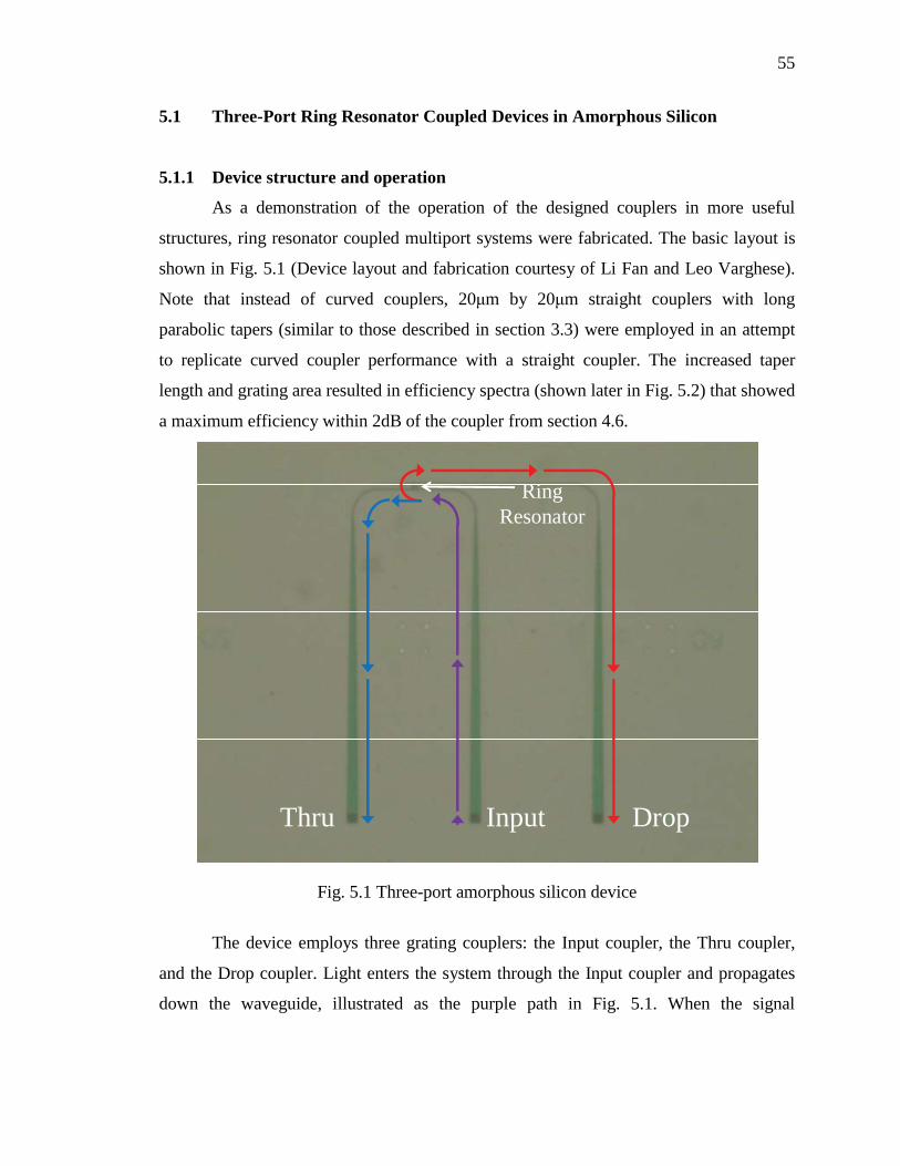
55
5.1 Three-Port Ring Resonator Coupled Devices in Amorphous Silicon
5.1.1 Device structure and operation
As a demonstration of the operation of the designed couplers in more useful
structures, ring resonator coupled multiport systems were fabricated. The basic layout is
shown in Fig. 5.1 (Device layout and fabrication courtesy of Li Fan and Leo Varghese).
Note that instead of curved couplers, 20 m by 20 m straight couplers with long
parabolic tapers (similar to those described in section 3.3) were employed in an attempt
to replicate curved coupler performance with a straight coupler. The increased taper
length and grating area resulted in efficiency spectra (shown later in Fig. 5.2) that showed
a maximum efficiency within 2dB of the coupler from section 4.6.
Fig. 5.1 Three-port amorphous silicon device
The device employs three grating couplers: the Input coupler, the Thru coupler,
and the Drop coupler. Light enters the system through the Input coupler and propagates
down the waveguide, illustrated as the purple path in Fig. 5.1. When the signal
Thru Input Drop
Ring Resonator

56
encounters the waveguide section near the ring resonator, a portion of the light resonantly
couples to the ring. As a result, a portion of the Input power is transferred to the ring.
Similarly, a portion of the light now in the ring will couple with the waveguide section of
the Drop port, and the power will be transferred as illustrated by the red path in Fig. 5.1.
The light not affected by the ring continues on to the Thru port, as illustrated by the blue
path in the figure.
Therefore, both the Thru and Drop couplers function as outputs for the device.
The Thru port outputs the light from the Input that hasn’t been coupled or lost due to ring
coupling, and the Drop port outputs the light that has successfully coupled through the
ring to the Drop waveguide. The ring coupling mechanism is not 100% efficient, and so
the addition of the Thru and Drop signals will be somewhat less than the Input signal.
5.1.2 Ring resonator coupling gap
The amount of power that is coupled from the Input to the Drop port is heavily
dependent on the separation between the waveguide sections and the ring. As mentioned
in section 4.2.1, the low response from the ring in the devices presented in chapter 4 was
a result of the 200nm coupling gap. This gap size was the optimal for quasi-TM coupling,
but as quasi-TE coupling was being used, ring response was quite poor.
In order to determine the adequate coupling distance for the quasi-TE
polarization, three-port devices with coupling gaps from 60-300nm were tested. The ring
response is also heavily wavelength dependent, and only occurs for wavelengths that
result in standing waves within the ring. For the particular ring diameter of 10 m used
here, the average spacing between dips on all devices was roughly 17nm, giving
approximately 5 dips across the wavelength spectrum. The maximum power loss of these
dips was recorded for each ring spacing. The maximum was used, as opposed to an
average, because a decrease in ring response at a particular wavelength for a given
coupling gap is driven largely by fabrication imperfection, and as a result is not
consistent across devices. These maxima are shown in Table 5.1.
The largest response was achieved with a coupling gap of 60nm. Note that due to
ring coupling losses, not all of this power is transferred to the Drop port. Only by
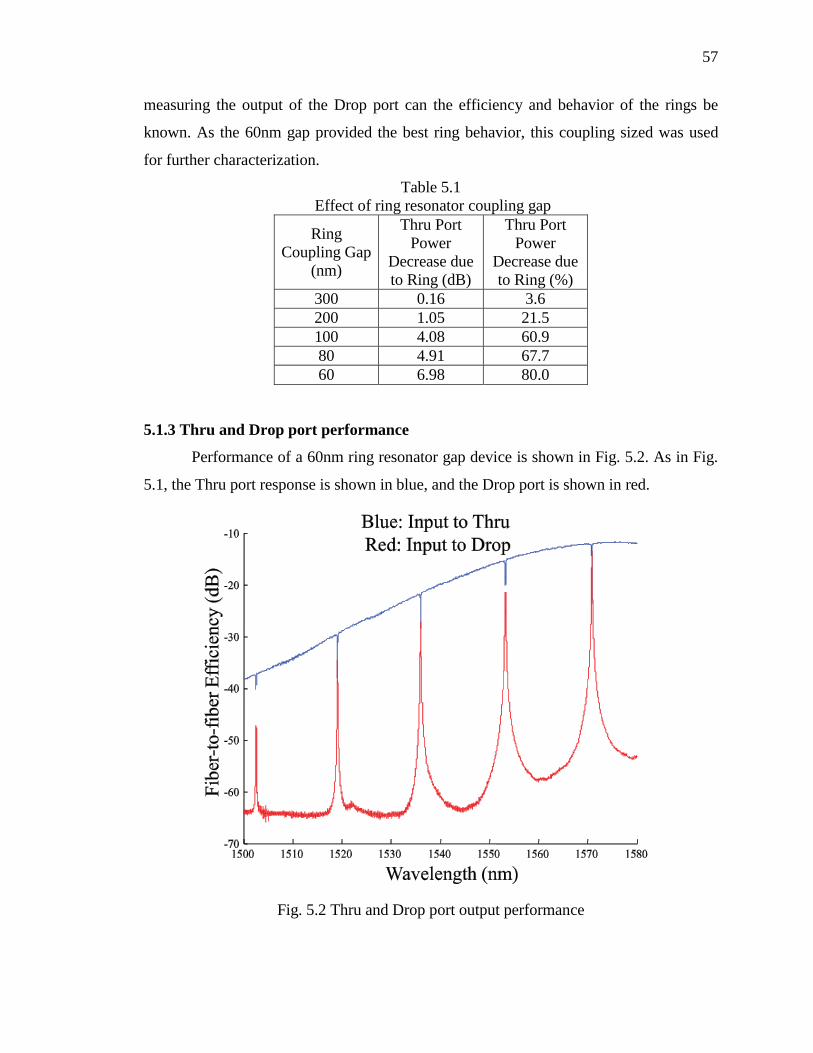
57
measuring the output of the Drop port can the efficiency and behavior of the rings be
known. As the 60nm gap provided the best ring behavior, this coupling sized was used
for further characterization.
Table 5.1 Effect of ring resonator coupling gap
Ring Coupling Gap
(nm)
Thru Port Power
Decrease due to Ring (dB)
Thru Port Power
Decrease due to Ring (%)
300 0.16 3.6 200 1.05 21.5 100 4.08 60.9 80 4.91 67.7 60 6.98 80.0
5.1.3 Thru and Drop port performance
Performance of a 60nm ring resonator gap device is shown in Fig. 5.2. As in Fig.
5.1, the Thru port response is shown in blue, and the Drop port is shown in red.
Fig. 5.2 Thru and Drop port output performance
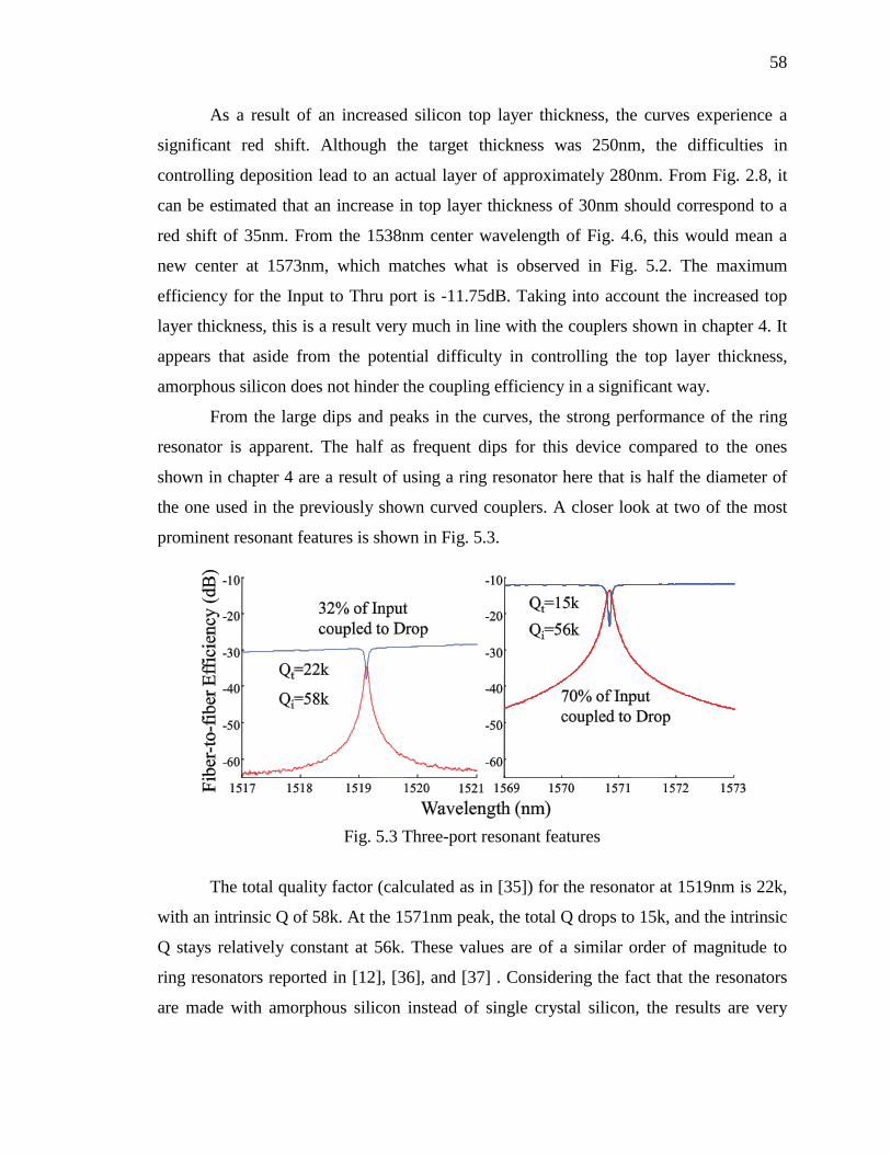
58
As a result of an increased silicon top layer thickness, the curves experience a
significant red shift. Although the target thickness was 250nm, the difficulties in
controlling deposition lead to an actual layer of approximately 280nm. From Fig. 2.8, it
can be estimated that an increase in top layer thickness of 30nm should correspond to a
red shift of 35nm. From the 1538nm center wavelength of Fig. 4.6, this would mean a
new center at 1573nm, which matches what is observed in Fig. 5.2. The maximum
efficiency for the Input to Thru port is -11.75dB. Taking into account the increased top
layer thickness, this is a result very much in line with the couplers shown in chapter 4. It
appears that aside from the potential difficulty in controlling the top layer thickness,
amorphous silicon does not hinder the coupling efficiency in a significant way.
From the large dips and peaks in the curves, the strong performance of the ring
resonator is apparent. The half as frequent dips for this device compared to the ones
shown in chapter 4 are a result of using a ring resonator here that is half the diameter of
the one used in the previously shown curved couplers. A closer look at two of the most
prominent resonant features is shown in Fig. 5.3.
Fig. 5.3 Three-port resonant features
The total quality factor (calculated as in [35]) for the resonator at 1519nm is 22k,
with an intrinsic Q of 58k. At the 1571nm peak, the total Q drops to 15k, and the intrinsic
Q stays relatively constant at 56k. These values are of a similar order of magnitude to
ring resonators reported in [12], [36], and [37] . Considering the fact that the resonators
are made with amorphous silicon instead of single crystal silicon, the results are very
59
good. These are values more than large enough to make useful devices with [38]. The
results for the power coupled at the given peaks are shown in table 5.2.
Table 5.2 Three-port signal distribution
1519nm 1571nm Power from
Input to dB % Power from Input to dB %
Thru -8.3 14.8 Thru -11.4 7.3 Drop -5 31.7 Drop -1.5 70.3 Loss -3.3 53.5 Loss -1.1 22.4
It can be seen that at both wavelengths a significant amount of power is coupled
to the Drop port. The main difference is the much higher loss at 1519nm than at 1571nm,
where the vast majority of the light is coupled to the Drop port. Even with this added
loss, however, the amount of power coupled through the ring for both wavelengths shows
that the use of ring coupled devices in amorphous silicon, making use of grating couplers
for low loss input and output, is very much possible. Although only 3 input/output ports
were used in this design, it could easily be expanded to include many more, or, under a
modified design, operate as a wavelength selective multiplexer.
5.2 One Dimensional Photonic Crystal Cavity
5.1.1 Device structure and operation
Demonstration of the use of the designed couplers with an actual test device,
created to test device structure properties and not the properties of the couplers used with
it, was carried out with a one dimensional photonic crystal cavity (1D PhC) [39]. The
device layout is shown in Fig. 5.4. Using specifically sized holes in the waveguide, a
strong bistable cavity [34] is created. Because of this bistability, the resonant frequency
of light entering the cavity depends upon which end of the cavity the light entered from.
The device shown here is created with the particular interest of investigating the thermal
non-linearity [40] of the device, which may contribute to the cavity bistability. Layout,
fabrication, and characterization of the device was done by Leo Varghese and Li Fan.
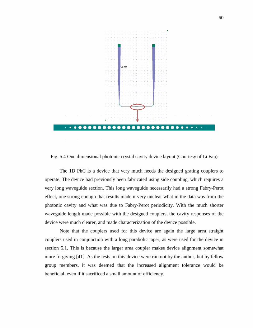
60
Fig. 5.4 One dimensional photonic crystal cavity device layout (Courtesy of Li Fan)
The 1D PhC is a device that very much needs the designed grating couplers to
operate. The device had previously been fabricated using side coupling, which requires a
very long waveguide section. This long waveguide necessarily had a strong Fabry-Perot
effect, one strong enough that results made it very unclear what in the data was from the
photonic cavity and what was due to Fabry-Perot periodicity. With the much shorter
waveguide length made possible with the designed couplers, the cavity responses of the
device were much clearer, and made characterization of the device possible.
Note that the couplers used for this device are again the large area straight
couplers used in conjunction with a long parabolic taper, as were used for the device in
section 5.1. This is because the larger area coupler makes device alignment somewhat
more forgiving [41]. As the tests on this device were run not by the author, but by fellow
group members, it was deemed that the increased alignment tolerance would be
beneficial, even if it sacrificed a small amount of efficiency.

61
5.2.2 Cavity performance
A view of a device peak near 1533nm is shown in Fig. 5.5. The device bistability
is seen in the peak difference between the “Forward” and “Backward” results at 5dBm
input power. The nonlinearity of the cavity is seen in the dramatic difference in effect
between the 5dBm results, which show at shift of around 50pm, and the -5dBm results,
which show almost no discernable shift. Indeed, a strong effect bistability is only seen at
the 5dBm level.
Fig. 5.5 One dimensional photonic crystal cavity bistability response (Courtesy of Li Fan)
5.2.2 Coupling performance
A sample wavelength spectrum for the device is shown in Fig. 5.6. As the input
power ranges from 5dBm to -5dBm and the output power peaks at -33dBm, the fiber-to-
fiber loss of 26dB for the device is significantly higher than the 12dB loss for couplers of
similar design explored in section 5.1. This is partially the result of the fiber v-groove
array being intentionally farther from the sample, which significantly decreases the
chance of chip contact at the expense of some added loss. From Fig. 4.9, the loss at a safe

62
100 m chip-to-fiber separation is about 7dB greater than for close coupling. Loss due to
the 1D PhC could potentially be near 1.5dB [34]. Together these account for the majority
of the additional loss, and the remaining 5.5dB is attributed to fabrication imperfection.
The initial amorphous silicon deposition left too thick of a layer of silicon, some of which
later had to be removed with dry etching. This harsh removal of material would have
significantly upset the performance of the device, and the result can be seen in the
correspondingly lower coupling efficiency.
Fig. 5.6 One dimensional photonic crystal spectrum (Courtesy of Li Fan)
Despite the increased fiber-to-fiber loss of the coupler here compared with
performance in chapter 4, the designed grating couplers performed as they were required
to for the purpose of this device. The small Fabry-Perot effect seen in Figs. 5.5 and 5.6
does not hinder the device characterization at all, whereas peak-to-peak variation of 5dB
or more was present for side coupled tests. Truly, the use of the designed grating couplers
is what made characterization of this device possible.

63
6. CONCLUSION AND FUTURE WORK
In this research, a low loss vertical grating coupler for use with silicon
nanophotonic devices was desired. Initial requirements were couplers that achieved
quasi-TE mode coupling with less than 10dB fiber-to-fiber loss and 3dB bandwidth cover
the C-band with 250nm silicon top layer wafers using 3 m of buried oxide, with the
eventual purpose of use in devices for testing. Starting with a base reference design from
literature, the effect of the changed silicon top layer thickness and buried oxide depth
were simulated. It was found that increased thicknesses compared with reference designs
would increase efficiency. Then, the effects of varying the design parameters of grating
periodicity, etch depth, fill factor, and coupling angle were explored. After parameter
simulations, a grating coupler structure was designed with optimized parameters for the
lowest loss at the desired center wavelength and over an adequate bandwidth.
An experimental system was developed to be used in conjunction with the
designed coupler. A fiber v-groove array was used to allow for multiple input and
outputs, and was mounted on a stage with fine precision and adequate positioning
control. The alignment of this mounting was verified via microscope to ensure proper
chip alignment. Straight and curved grating coupler layouts were then developed.
The fabricated grating coupler test chips were then characterized in terms of
efficiency, as well as the Fabry-Perot effect of the couplers resulting from a small cavity
size. Using a more useful fiber v-groove, the devices were recharacterized, and
consistently performed at the required loss level with bandwidths that significantly
exceeded project requirements. The coupler consistency was then investigated in terms of
input stability, mechanical stability, and coupling gap effect. It was found that meeting
the project goals had not been a fluke, and that the fabricated couplers consistently met
required performance. Additionally, the fabricated coupler performance exceeded the
published results in terms of efficiency and bandwidth.
64
With the desired coupler behavior achieved, use of the couplers in practical
devices was explored. These devices went beyond the project requirements, and showed
the use of the designed gratings in amorphous silicon top layer devices. A three-port ring
resonator coupled structure was tested, and the optimal ring coupling gap for quasi-TE
performance was found. This allowed for high efficiency interwaveguide signal transfer
via ring resonator, and demonstrated the potential use of the designed grating couplers in
multiple input and output multiplexer systems. The use of the coupler with a one
dimensional photonic crystal cavity was then explored. This was a device that had
previous been tried using side coupling, but characterization proved impossible due to the
necessarily long waveguide length. Utilizing the potential short waveguide possible with
grating couplers, the device was able to be characterized successfully.
Therefore, it is concluded that the designed couplers met the project goals. They
proved to be a tool for consistent low loss fiber-to-chip in and out coupling. Additionally,
their use in two different device structures showed the grating system was ready for use
as the input and output method for test devices.
Future work with grating couplers will focus on increasing efficiency, using the
coupler’s Fabry-Perot effect, and the realization of flexible devices using amorphous
silicon. Attempts at increasing efficiency will explore the effect of the grating curvature
in curved couplers, and combining a maximally efficient focus design with an increased
silicon top layer thickness to potentially increase the coupling efficiency [22]. The device
characterization in chapter 4 revealed that complex Fabry-Perot peaks exist for each
unique device that are consistent in shape and detail regardless of the input power or
specific alignment. Utilizing an appropriate signal normalization technique, this
consistency could potentially be used to uniquely identify specific devices by their unique
Fabry-Perot waveforms. With regards to amorphous silicon, the ability to deposit silicon
and silicon dioxide on a substrate instead of being bound to a particular wafer allows the
use of substrate materials other than silicon. The use of a flexible polymer that can stand
up to the needs of fabrication and processing, combined with intelligent device design,
could result in flexible nanophotonic devices.

LIST OF REFERENCES
65
LIST OF REFERENCES
[1] S. Xiao et al., "Compact silicon microring resonators with ultra-low propagation loss in the C band," Optics Express, vol. 15, no. 22, pp. 14467-14475, Oct 2007.
[2] P. Dong al., "Low loss shallow-ridge silicon waveguides," Optics Express, vol. 18, no. 14, pp. 14474-14479, Jul 2010.
[3] F. Xia, L. Sekaric, and Y. Vlasov, "Ultracompact optical buffers on a silicon chip," Nature Photonics, vol. 1, pp. 65-71, 2007.
[4] Q. Xu and M. Lipson, "All-optical logic based silicon micro-rong resonators," Optics Express, vol. 15, no. 3, pp. 924-929, Feb 2007.
[5] G. T. Reed et al., "Silicon optical modulators," Nature Photonics, vol. 4, pp. 518-526, 2010.
[6] M. H. Khan et al., "Ultrabroad-bandwidth arbitrary radiofrequency waveform generation with a silicon photonic chip-based spectral shaper," Nature Photonics, vol. 4, pp. 117-122, 2010.
[7] M. A. Foster et al., "Silicon-chip-based ultrafast optical oscilloscope," Nature, vol. 456, pp. 81-84, Nov 2008.
[8] F. Dell'Olio and V. M. N. Passaro, "Optical sensing by optimized silicon slot waveguides," Optics Express, vol. 15, no. 8, pp. 4977-4993, Apr 2007.
[9] M. A. Foster et al., "Broad-band optical parametric gain on a silicon photonic chip," Nature, vol. 441, pp. 960-963, 2006.
[10] V. Sih et al., "Raman amplification of 40 Gb/s data in low-loss silicon waveguides," Optics Express, vol. 15, no. 12, pp. 357-362, Jan 2007.
[11] Corning. (2011, July) Corning SMF-28e+ Optical Fiber. [Online]. http://www.corning.com/WorkArea/showcontent.aspx?id=40723
66
[12] T. Tsuchizawa et al., "Microphotonics devices based on silicon microfabrication technology," IEEE Journal of Selected Topics in Quantum Electronics, vol. 11, no. 1, pp. 232-240, Jan-Feb 2005.
[13] V. Nguyen et al., "Silicon-based highly-efficient fiber-to-waveguide coupler for high index contrast systems," Applied Physics Letters, vol. 88, Feb 2006.
[14] V. R. Almeida et al., "Nanotaper for compact mode conversion," Optics Letter, vol. 28, no. 15, pp. 1302-1304, Aug 2003.
[15] G. Roelkens et al., "High efficiency Silicon-on-Insulator grating coupler based on a poly-Silicon overlay," Optics Express, vol. 14, no. 24, pp. 11622-11630, Nov 2006.
[16] D. Taillaert et al., "Compact efficient broadband grating coupler for silicon-on-insulator waveguides," Optics Letters, vol. 29, no. 23, pp. 2749-2751, Dec 2004.
[17] Graham T. Reed, Silicon photonics: the state of the art, 1st ed. West Sussex, UK: Wiley-Interscience, 2008.
[18] M. L. Dakes, "Grating Coupler for Efficient Excitation of Optical Guided Waves in Thin Films," Applied Physics Letters, vol. 16, no. 12, pp. 523-525, Jun 1970.
[19] F. Van Laere et al., "Compact Focusing Grating Couplers Between Optical Fibers and Silicon-On-Insulator Photonic Wire Waveguides," in Optical Fiber Communication and the National Fiber Optic Engineers Conference, Anaheim, CA, 2007, pp. 1-3.
[20] W. Bogaerts et al., "Basic structures for photonic integrated circuits in silicon-on-insulator," Optics Express, vol. 12, no. 8, pp. 1583-1591, Apr 2004.
[21] R. Waldhausl et al., "Efficient coupling into polymer waveguides by gratings," Applied Optics, vol. 36, no. 36, pp. 9383-9390, Dec 1997.
[22] J. H. Harris et al., "Theory and Design of Periodic Couplers," Applied Optics, vol. 11, no. 10, pp. 2234-2241, Oct 1972.
[23] D. F. G. Gallagher and T. P. Felici, "Eigenmode expansion methods for simulation of optical propagation in photonics - Pros and cons," in Conference on Integrated Optics - Device, Materials and Technologies VII, San Jose, CA, 2003, pp. 69-82.
67
[24] Dirk Taillaert, "Grating couplers as Interface between Optical Fibers and Nanophotonic Waveguides," Ph.D. dissertation, INTEC, Ghent Univ., Ghent, Netherlands, 2004.
[25] V. A. Sychugov et al., "Optimization and control of grating coupling to or from a silicon-based optical waveguide," Optical Engineering, vol. 35, no. 11, pp. 3092-3100, Nov 1996.
[26] S. Ramo et al., Fields and Waves in Communication Electronics, 3rd ed. New York: Wiley, 1993.
[27] F. Van Laere et al., "Compact Focusing Grating Couplers for Silicon-on-Insulator Integrated Circuits," IEEE Photonics Technology Letters, vol. 19, no. 21-24, pp. 1919-1921, Nov-Dec. 2007.
[28] P. Bienstman. (2007, August) CAMFR 1.3 Prerelease, CAvity Modeling FRamework. [Online]. http://camfr.sourceforge.net/
[29] M. Y. Fan et al., "High Directivity, Vertical Fiber-to-Chip Coupler with Anisotropically Radiating Grating Teeth," in Conference on Lasers & Electro-Optics/Quantum Electronics and Laser Science, Baltimore, MD, 2007, pp. 791-792.
[30] S. K. Selvaraja et al., "Highly efficient grating coupler between optical fiber and silicon photonic circuit," in Conference on Lasers and Electro-Optics and Quantim Electronics and Laser Science, Baltimore, MD, 2009, pp. 1293-1294.
[31] Optics, OZ. (2009, March) V-groove assemblies. [Online]. http://www.ozoptics.com/ALLNEW_PDF/DTS0083.pdf
[32] E. Hecht, Optics, 4th ed. San Francisco, CA: Addison Wesley, 2002.
[33] X. Ni, Z. Liu, A. V. Kildishev Kildishev. (2010) PhotonicsDB: Optical Constants. [Online]. http://nanohub.org/resources/PhotonicsDB
[34] Q. Quan et al., "Photonic crystal nanobeam cavity strongly coupled to the feeding waveguide," Applied Physics Letters, vol. 96, no. 20, May 2010.
[35] S. Xiao et al., "Modeling and measurements of losses in silicon-on-insulator resonators and bends," Optics Express, vol. 15, no. 17, pp. 10553-10561, Aug 2007.
[36] J. Niehusmann et al., "Ultrahigh-quality-factor silicon-on-insulator microring resonator," Optics Letters, vol. 29, no. 24, pp. 2861-2868, 2004.
68
[37] Q. Xu et al., "Breaking the delay-bandwidth limit in a photonic structure," Nature Physics, vol. 3, pp. 406-410, April 2007.
[38] F. Xia et al., "Ultracompact optical buffers on a silicon chip," Nature Photonics, vol. 1, pp. 65-71, 2007.
[39] J. S. Foresi et al., "Photonic-bandgap microcavities in optical waveguides," Nature, vol. 390, pp. 143-145, Nov 1997.
[40] M. Brunstein et al., "Thermo-optical dynamics in an optically pumped Photonic Crystal nano-cavity," Optics Express, vol. 17, no. 19, pp. 17118-17129, Sep 2009.
[41] J. M. Lee et al., "Enhancing alignment tolerance of silicon waveguide by using a wide grating coupler," Optics Express, vol. 16, no. 17, pp. 13024-13031, Aug 2008.