deposited low temperature silicon ghz modulator low temperature silicon ghz modulator yoon ho daniel...
TRANSCRIPT
Deposited low temperature silicon GHz modulator
Yoon Ho Daniel Lee,1 Michael O. Thompson,2 and Michal Lipson1,3,* 1Cornell Nanophotonics Group, School of Electrical and Computer Engineering, Cornell University, Ithaca, New
York 14853, USA 2Department of Materials Science and Engineering, Cornell University, Ithaca, New York 14853, USA
3Kavli Institute at Cornell, Cornell University, Ithaca, New York 14853, USA *[email protected]
Abstract: We demonstrate gigahertz electro-optic modulator fabricated on low temperature polysilicon using excimer laser annealing technique compatible with CMOS backend integration. Carrier injection modulation at 3 Gbps is achieved. These results open up an array of possibilities for silicon photonics including photonics on DRAM and on flexible substrates.
©2013 Optical Society of America
OCIS codes: (200.4650) Optical interconnects; (250.4110) Modulators; (310.1860) Deposition and fabrication.
References and links
1. J. S. Orcutt, A. Khilo, C. W. Holzwarth, M. A. Popović, H. Li, J. Sun, T. Bonifield, R. Hollingsworth, F. X. Kärtner, H. I. Smith, V. Stojanović, and R. J. Ram, “Nanophotonic integration in state-of-the-art CMOS foundries,” Opt. Express 19(3), 2335–2346 (2011).
2. S. Sridaran and S. A. Bhave, “Nanophotonic devices on thin buried oxide silicon-on-insulator substrates,” Opt. Express 18(4), 3850–3857 (2010).
3. B. R. Moss, S. Chen, M. Georgas, J. Shainline, J. S. Orcutt, J. C. Leu, M. Wade, C. Yu-Hsin, K. Nammari, W. Xiaoxi, L. Hanqing, R. Ram, M. A. Popovic, and V. Stojanovic, “A 1.23pJ/b 2.5Gb/s monolithically integrated optical carrier-injection ring modulator and all-digital driver circuit in commercial 45nm SOI,” in Solid-State Circuits Conference Digest of Technical Papers (ISSCC), 2013 (IEEE International, 2013), pp. 126–127.
4. J. M. Shainline, J. S. Orcutt, M. T. Wade, K. Nammari, B. Moss, M. Georgas, C. Sun, R. J. Ram, V. Stojanović, and M. A. Popović, “Depletion-mode carrier-plasma optical modulator in zero-change advanced CMOS,” Opt. Lett. 38(15), 2657–2659 (2013).
5. T. Baehr-Jones, T. Pinguet, P. Lo Guo-Qiang, S. Danziger, D. Prather, and M. Hochberg, “Myths and rumours of silicon photonics,” Nat. Photonics 6(4), 206–208 (2012).
6. J. M. Shainline, J. S. Orcutt, M. T. Wade, K. Nammari, O. Tehar-Zahav, Z. Sternberg, R. Meade, R. J. Ram, V. Stojanović, and M. A. Popović, “Depletion-mode polysilicon optical modulators in a bulk complementary metal-oxide semiconductor process,” Opt. Lett. 38(15), 2729–2731 (2013).
7. D. J. Shin, K. S. Cho, H. C. Ji, B. S. Lee, S. G. Kim, J. K. Bok, S. H. Choi, Y. H. Shin, J. H. Kim, S. Y. Lee, K. Y. Cho, B. J. Kuh, J. H. Shin, J. S. Lim, J. M. Kim, H. M. Choi, K. H. Ha, Y. D. Park, and C. H. Chung, “Integration of Si photonics into DRAM process,” in Optical Fiber Communication Conference/National Fiber Optic Engineers Conference 2013, OSA Technical Digest (online) (Optical Society of America, 2013), pp. OTu2C.4.
8. A. Hosseini, B. Fallahazad, D. N. Kwong, Y. Zhang, E. Tutuc, and R. T. Chen, “A platform for three-dimensional on-chip photonics: Multi-bonded silicon-on-insulator wafers,” in 2011 Conference on Lasers and Electro-Optics (CLEO), 2011, pp. 1–2.
9. A. E.-J. Lim, T.-Y. Liow, N. Duan, L. Ding, M. Yu, G. Q. Lo, and D. L. Kwong, “Germanium electro-absorption modulator for power efficient optical links,” in Microwave Photonics, 2011 International Topical Meeting on & Microwave Photonics Conference, 2011 Asia-Pacific (MWP/APMP, 2011), pp. 105–108.
10. Y. Chen, H. Li, and M. Li, “Flexible and tunable silicon photonic circuits on plastic substrates,” Sci. Rep. 2, 622 (2012).
11. A. V. Rylyakov, C. L. Schow, B. G. Lee, W. M. J. Green, S. Assefa, F. E. Doany, M. Yang, J. Van Campenhout, C. V. Jahnes, J. A. Kash, and Y. A. Vlasov, “Silicon photonic switches hybrid-integrated with CMOS drivers,” IEEE J. Solid State Circuits 47(1), 345–354 (2012).
12. A. L. Glebov, H. D. Thacker, I. Shubin, Y. Luo, J. Costa, J. Lexau, X. Zheng, G. Li, J. Yao, D. Patil, F. Liu, R. Ho, T. Pinguet, P. Dong, D. Feng, M. Asghari, K. Raj, J. G. Mitchell, A. V. Krishnamoorthy, J. E. Cunningham, and R. T. Chen, “Hybrid-integrated silicon photonic bridge chips for ultralow-energy inter-chip communications,” Proc. SPIE 7944, 79440B (2011).
13. L. Alloatti, D. Korn, R. Palmer, D. Hillerkuss, J. Li, A. Barklund, R. Dinu, J. Wieland, M. Fournier, J. Fedeli, H. Yu, W. Bogaerts, P. Dumon, R. Baets, C. Koos, W. Freude, and J. Leuthold, “42.7 Gbit/s electro-optic modulator in silicon technology,” Opt. Express 19(12), 11841–11851 (2011).
#195502 - $15.00 USD Received 13 Aug 2013; revised 21 Oct 2013; accepted 21 Oct 2013; published 29 Oct 2013(C) 2013 OSA 4 November 2013 | Vol. 21, No. 22 | DOI:10.1364/OE.21.026688 | OPTICS EXPRESS 26688
14. M. Melchiorri, N. Daldosso, F. Sbrana, L. Pavesi, G. Pucker, C. Kompocholis, P. Bellutti, and A. Lui, “Propagation losses of silicon nitride waveguides in the near-infrared range,” Appl. Phys. Lett. 86(12), 121111 (2005).
15. N. Sherwood-Droz and M. Lipson, “Scalable 3D dense integration of photonics on bulk silicon,” Opt. Express 19(18), 17758–17765 (2011).
16. S. Rao, G. Coppola, M. A. Gioffrè, and F. G. Della Corte, “A 2.5 ns switching time MachZehnder modulator in as-deposited a-Si:H,” Opt. Express 20(9), 9351–9356 (2012).
17. A. M. Agarwal, M. R. Black, J. S. Foresi, L. Liao, Y. Liu, and L. C. Kimerling, “Polysilicon waveguides for silicon photonics,” MRS Proc. 403 (1995).
18. J. S. Orcutt, S. D. Tang, S. Kramer, K. Mehta, H. Li, V. Stojanović, and R. J. Ram, “Low-loss polysilicon waveguides fabricated in an emulated high-volume electronics process,” Opt. Express 20(7), 7243–7254 (2012).
19. K. Preston, S. Manipatruni, A. Gondarenko, C. B. Poitras, and M. Lipson, “Deposited silicon high-speed integrated electro-optic modulator,” Opt. Express 17(7), 5118–5124 (2009).
20. P. M. Smith, P. G. Carey, and T. W. Sigmon, “Excimer laser crystallization and doping of silicon films on plastic substrates,” Appl. Phys. Lett. 70(3), 342–344 (1997).
21. R. Delmdahl, “The excimer laser: Precision engineering,” Nat. Photonics 4(5), 286 (2010). 22. Q. Xu, S. Manipatruni, B. Schmidt, J. Shakya, and M. Lipson, “12.5 Gbit/s carrier-injection-based silicon micro-
ring silicon modulators,” Opt. Express 15(2), 430–436 (2007).
1. Introduction
The majority of silicon photonics is built on silicon-on-insulator (SOI) wafers while the majority of electronics, including CPUs and memory, are built on bulk silicon wafers, limiting broader acceptance of silicon photonics. This discrepancy is a result of silicon photonics’ requirement for a single-crystalline silicon (c-Si) layer and a thick undercladding for optical guiding that bulk silicon wafers do not provide. While the undercladding problem can be partially addressed by substrate removal techniques [1–4], the complexity and compromises of co-integrating photonics with state-of-the-art transistors and DRAM [5–7] and real estate competition between electronics and photonics remain problematic.
Previous attempts at integrating silicon photonics with bulk CMOS include localized substrate removal [1] and bonding techniques [8], but process compatibility, scalability and manufacturability have hindered these approaches from mainstream adoption. Localized substrate removal involves using XeF2 gas to isotropically undercut the bulk silicon substrate underneath the waveguide to prevent optical leakage into the substrate. However, it limits potential for independent optimization of electrical polysilicon and optical polysilicon due to thermal budget constraints. A germanium electro-absorption modulator has also been demonstrated [9], but it requires a crystalline silicon layer as well as thermal processing at 550þC. Other approaches involve transfer or bonding of thin films, individual devices, or complete dies. Bonding of patterned crystalline silicon [8] allows single crystalline material on CMOS BEOL, but it does not reduce the high thermal budget required for dopant activation to fabricate active devices. For transfer of completely fabricated devices [10], yield and alignment tolerance remain challenging. Flip-chip bonding of a complete SOI photonic die [11,12] onto an electronics die has also been used due to the maturity of flip-chip bonding technology. However, flip-chip bonding suffers from additional electrical parasitics, limited architectural freedom, and higher cost.
2. Deposited polysilicon
There are several low loss optical materials that can be deposited and therefore facilitate integration of photonics on arbitrary substrates, but their high band gap and low mobility precludes these materials from enabling active devices such as modulator and switches. Examples of such materials include polymers [13], Silicon Nitride (SiN) [14,15] and hydrogenated amorphous silicon (a-Si:H) [16]. SiN is a dielectric with bandgap of 5 eV making it electrically inactive, and a-Si:H with its inherently high defect density and low mobility requires high voltage incompatible with latest CMOS transistors and is unable to operate at gigahertz speed. Polymer has low upper thermal processing limit, and high poling voltage (> 10 V) is needed for poling of polymer, posing compatibility and reliability issues for system integration. Furthermore, active polymer devices require c-Si waveguide for its operation, which makes backend integration difficult.
#195502 - $15.00 USD Received 13 Aug 2013; revised 21 Oct 2013; accepted 21 Oct 2013; published 29 Oct 2013(C) 2013 OSA 4 November 2013 | Vol. 21, No. 22 | DOI:10.1364/OE.21.026688 | OPTICS EXPRESS 26689
Polysilicon is a low loss material that is deposited and could in principle enable high performance active devices, but it traditionally exhibited much lower performance than its crystalline counterpart. Polysilicon is a collection of grains of c-Si separated by grain boundaries consisting of a few atomic layers of amorphous material. Grain boundaries not only act as small perturbations causing photon and electron scattering, but also create states within the silicon bandgap that cause excess optical loss. Since the groundbreaking work on polysilicon photonics [17], much progress has been made, including active devices. Various works using high temperature annealed polysilicon have demonstrated low loss on the order of 10 dB/cm [18], and electro-optic modulation [6,7,19] has also been shown. However, these works are not compatible with CMOS backend integration due to their high thermal budget fundamental to furnace annealed polysilicon, constraining them to frontend integration in CMOS and DRAM.
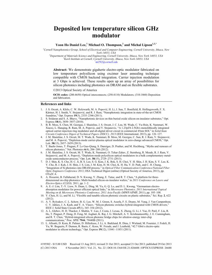
Fig. 1. Backend deposited silicon photonics. Rendered image of polysilicon modulator integrated on CMOS BEOL. For clarity, we show only a part of the metal contacts. One can see that the grain boundaries and the dimensions of the cross-section of the device are comparable.
We demonstrate high performance deposited silicon photonics on a thin film of low temperature polysilicon by tailoring the dimensions of the grain boundaries to be similar to the dimensions of the cross-sections of nanophotonic devices. By ensuring that the number of grain boundaries across the cross-section of the waveguide is small, the electrical properties of the device are expected to be comparable to its single crystalline counterpart, and the optical properties to be sufficient for high quality factor resonators. The tailoring of the grain sizes is done by using Excimer Laser Anneal (ELA), which involves irradiation of a deposited thin film of a-Si with a short UV laser pulse, which is absorbed completely within the first tens of nm due to high absorption coefficient of a-Si at UV wavelengths. Due to the very short duration and confinement of heat close to the surface, underlying device structures receive a minimal increase in the total thermal budget, while the a-Si film heats up enough to melt and re-solidify, crystallizing into polysilicon. In fact, the thermal impact is so small that ELA has been successfully performed even on a plastic substrate with 120 þC thermal processing limit [20]. This local heating enables ELA to be performed in the CMOS backend without affecting the electronics underneath as illustrated in Fig. 1, decoupling the CMOS frontend from photonics. Furthermore, excimer laser annealing is an industry proven technology in the flat panel industry with throughput equivalent to over five hundred 300 mm
#195502 - $15.00 USD Received 13 Aug 2013; revised 21 Oct 2013; accepted 21 Oct 2013; published 29 Oct 2013(C) 2013 OSA 4 November 2013 | Vol. 21, No. 22 | DOI:10.1364/OE.21.026688 | OPTICS EXPRESS 26690
wafers per hour, well exceeding that of state of the art CMOS lithography tools [21]. Once ELA is performed on the wafer, the rest of the fabrication is performed using standard CMOS fabrication process, therefore requiring only one extra process module in a CMOS process.
3. Fabrication and experimental results
We start fabrication on a silicon wafer with 4 µm of thermal oxide. Deposition of 150 nm of undoped PECVD a-Si under 400 þC is performed by a commercial deposition service. A series of electron beam lithography and ion implantation is used to form N, N + + , P, and P + + regions using Phosphorous and Boron, respectively. The wafer is then furnace annealed at 450 þC for 1 hour in argon ambient to dehydrogenate the PECVD a-Si film, followed by excimer laser annealing using a laser pulse at wavelength of 308 nm with temporal FWHM of 35 ns generated by a XeCl excimer laser. This step crystallizes the initial layer of deposited a-Si into polysilicon and makes the dopants electrically active. Following ELA, excess surface roughness created by ELA is polished using Chemical Mechanical Polish (CMP). Waveguide and slab are defined by electron beam lithography and etched using reactive ion etching. The wafer is then clad with 1 µm of PECVD SiO2 at 400 þC, followed by electrical contact and pad formation. The thermal budget of the whole process flow is compatible with CMOS backend integration, with single dominant thermal budget of 1 hour at 450 þC for dehydrogenation. This thermal budget can in principle be significantly lowered by using multiple-step recrystallization [20] or evaporated material.
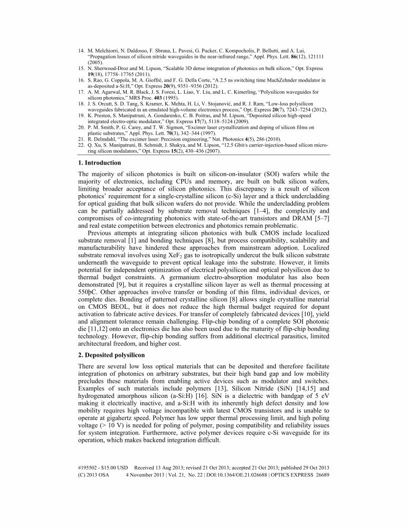
Fig. 2. Characterization of low temperature polysilicon devices. (a) Optical micrograph of the fabricated device (b) Transmission spectrum of polysilicon ring resonator with Qloaded ~12,000 (c) IV curve of the fabricated polysilicon ring modulator device.
We characterize passive ring resonators with radius of 20 µm to be suitable for up to 15 GHz modulation with high extinction ratio. The waveguide dimensions are 700 nm wide by 110 nm high with slab thickness of 40 nm for single mode transverse electric (TE) polarization operation. The waveguide has a high effective confinement factor of 0.78, which allows bending radius as tight as 5 µm yielding measured free spectral range of 26 nm. The low temperature ring resonators with radius of 20 µm have loaded Q-factor of 12,000, and 10 dB extinction ratio as shown in Fig. 2(b). Note that the loss of the polysilicon (estimated to be on the order of 20 dB/cm) affects only the extinction ratio (currently 10 dB due to undercoupling), and not the insertion loss.
We characterize the electrical properties of the modulators and show that ELA polysilicon has good dopant activation characteristics and c-Si-like behavior. The completed device is shown in Fig. 2(a). We measured the IV characteristics of polysilicon PN diode ring modulators with 20 μm radius and observed total series resistance of 25 Ω and low reverse leakage current of −62 nA at −5 V. The diode IV curve seen in Fig. 2(c) clearly shows exponential behavior in the low current regime below 0.8 V with diode ideality factor of 1.35 ± 0.1, followed by high injection and series resistance limited behavior. Ideality factor of 1.35 along with low normalized leakage current of −490 pA/µm demonstrate that ELA polysilicon has great dopant activation characteristics and crystalline silicon-like behavior that make this diode well suited for sensitive forward bias modulation. In addition, combination of low
#195502 - $15.00 USD Received 13 Aug 2013; revised 21 Oct 2013; accepted 21 Oct 2013; published 29 Oct 2013(C) 2013 OSA 4 November 2013 | Vol. 21, No. 22 | DOI:10.1364/OE.21.026688 | OPTICS EXPRESS 26691
leakage current and low series resistance would make ELA polysilicon an excellent platform for high speed reverse bias modulator.
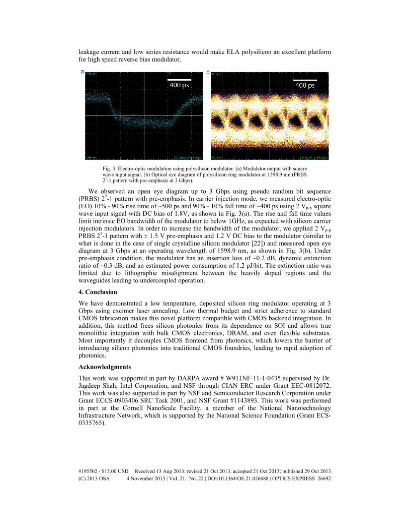
Fig. 3. Electro-optic modulation using polysilicon modulator. (a) Modulator output with square wave input signal. (b) Optical eye diagram of polysilicon ring modulator at 1598.9 nm (PRBS 27-1 pattern with pre-emphasis at 3 Gbps).
We observed an open eye diagram up to 3 Gbps using pseudo random bit sequence (PRBS) 27-1 pattern with pre-emphasis. In carrier injection mode, we measured electro-optic (EO) 10% - 90% rise time of ~500 ps and 90% - 10% fall time of ~400 ps using 2 Vp-p square wave input signal with DC bias of 1.8V, as shown in Fig. 3(a). The rise and fall time values limit intrinsic EO bandwidth of the modulator to below 1GHz, as expected with silicon carrier injection modulators. In order to increase the bandwidth of the modulator, we applied 2 Vp-p PRBS 27-1 pattern with ± 1.5 V pre-emphasis and 1.2 V DC bias to the modulator (similar to what is done in the case of single crystalline silicon modulator [22]) and measured open eye diagram at 3 Gbps at an operating wavelength of 1598.9 nm, as shown in Fig. 3(b). Under pre-emphasis condition, the modulator has an insertion loss of ~0.2 dB, dynamic extinction ratio of ~0.3 dB, and an estimated power consumption of 1.2 pJ/bit. The extinction ratio was limited due to lithographic misalignment between the heavily doped regions and the waveguides leading to undercoupled operation.
4. Conclusion
We have demonstrated a low temperature, deposited silicon ring modulator operating at 3 Gbps using excimer laser annealing. Low thermal budget and strict adherence to standard CMOS fabrication makes this novel platform compatible with CMOS backend integration. In addition, this method frees silicon photonics from its dependence on SOI and allows true monolithic integration with bulk CMOS electronics, DRAM, and even flexible substrates. Most importantly it decouples CMOS frontend from photonics, which lowers the barrier of introducing silicon photonics into traditional CMOS foundries, leading to rapid adoption of photonics.
Acknowledgments
This work was supported in part by DARPA award # W911NF-11-1-0435 supervised by Dr. Jagdeep Shah, Intel Corporation, and NSF through CIAN ERC under Grant EEC-0812072. This work was also supported in part by NSF and Semiconductor Research Corporation under Grant ECCS-0903406 SRC Task 2001, and NSF Grant #1143893. This work was performed in part at the Cornell NanoScale Facility, a member of the National Nanotechnology Infrastructure Network, which is supported by the National Science Foundation (Grant ECS-0335765).
#195502 - $15.00 USD Received 13 Aug 2013; revised 21 Oct 2013; accepted 21 Oct 2013; published 29 Oct 2013(C) 2013 OSA 4 November 2013 | Vol. 21, No. 22 | DOI:10.1364/OE.21.026688 | OPTICS EXPRESS 26692