sequential circuit design - university of...
TRANSCRIPT
1
Synchronous Sequential Circuit Review

Steps
2
4/3/2009 Page 3
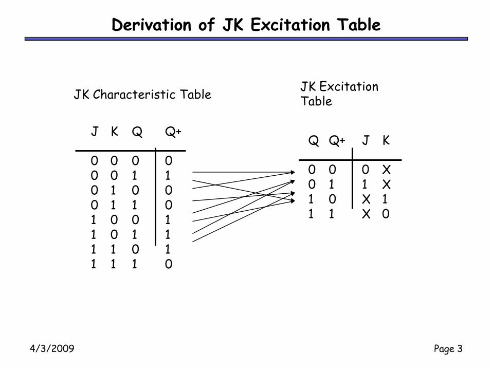
Derivation of JK Excitation Table
JK Characteristic TableJK Excitation Table
J
00001111
K
00110011
Q
01010101
Q+
01001110
Q+
0101
Q
0011
J
01XX
K
XX10
4/3/2009 Page 4
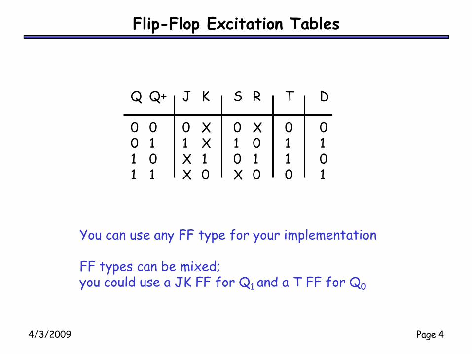
Flip-Flop Excitation Tables
Q+
0101
Q
0011
J
01XX
K
XX10
S
010X
R
X010
T
0110
D
0101
You can use any FF type for your implementation
FF types can be mixed; you could use a JK FF for Q1 and a T FF for Q0
5
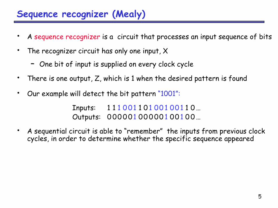
Sequence recognizer (Mealy)
• A sequence recognizer is a circuit that processes an input sequence of bits
• The recognizer circuit has only one input, X
– One bit of input is supplied on every clock cycle
• There is one output, Z, which is 1 when the desired pattern is found
• Our example will detect the bit pattern ―1001‖:
Inputs: 1 1 1 0 01 1 0 1 00 1 00 1 1 0 … Outputs: 0 00 0 01 00 0 00 1 00 1 0 0 …
• A sequential circuit is able to ―remember‖ the inputs from previous clock cycles, in order to determine whether the specific sequence appeared
6
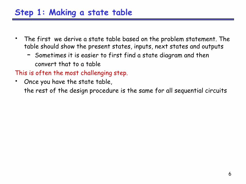
Step 1: Making a state table
• The first we derive a state table based on the problem statement. The table should show the present states, inputs, next states and outputs
– Sometimes it is easier to first find a state diagram and then
convert that to a table
This is often the most challenging step.
• Once you have the state table,
the rest of the design procedure is the same for all sequential circuits
7
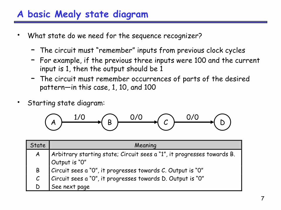
A basic Mealy state diagram
• What state do we need for the sequence recognizer?
– The circuit must ―remember‖ inputs from previous clock cycles
– For example, if the previous three inputs were 100 and the current input is 1, then the output should be 1
– The circuit must remember occurrences of parts of the desired pattern—in this case, 1, 10, and 100
• Starting state diagram:
A B C D1/0 0/0 0/0
State Meaning
A Arbitrary starting state; Circuit sees a ―1‖, it progresses towards B.
Output is ―0‖
B Circuit sees a ―0‖, it progresses towards C. Output is ―0‖
C Circuit sees a ―0‖, it progresses towards D. Output is ―0‖
D See next page

8
Overlapping occurrences of the pattern
• What happens if we’re in state D (the last three inputs were 100), and
the current input is 1?
– The output should be a 1, because we’ve found the desired pattern
– This last 1 could also be the start of another occurrence of the pattern! For example, 1001001 contains two occurrences of 1001
– To detect overlapping occurrences of the pattern, the next state
should be B.
A B C D1/0 0/0 0/0
1/1
State Meaning
A None of the desired pattern (1001) has been input yet.
B We’ve already seen the first bit (1) of the desired pattern.
C We’ve already seen the first two bits (10) of the desired pattern.
D We’ve already seen the first three bits (100) of the desired pattern.
9
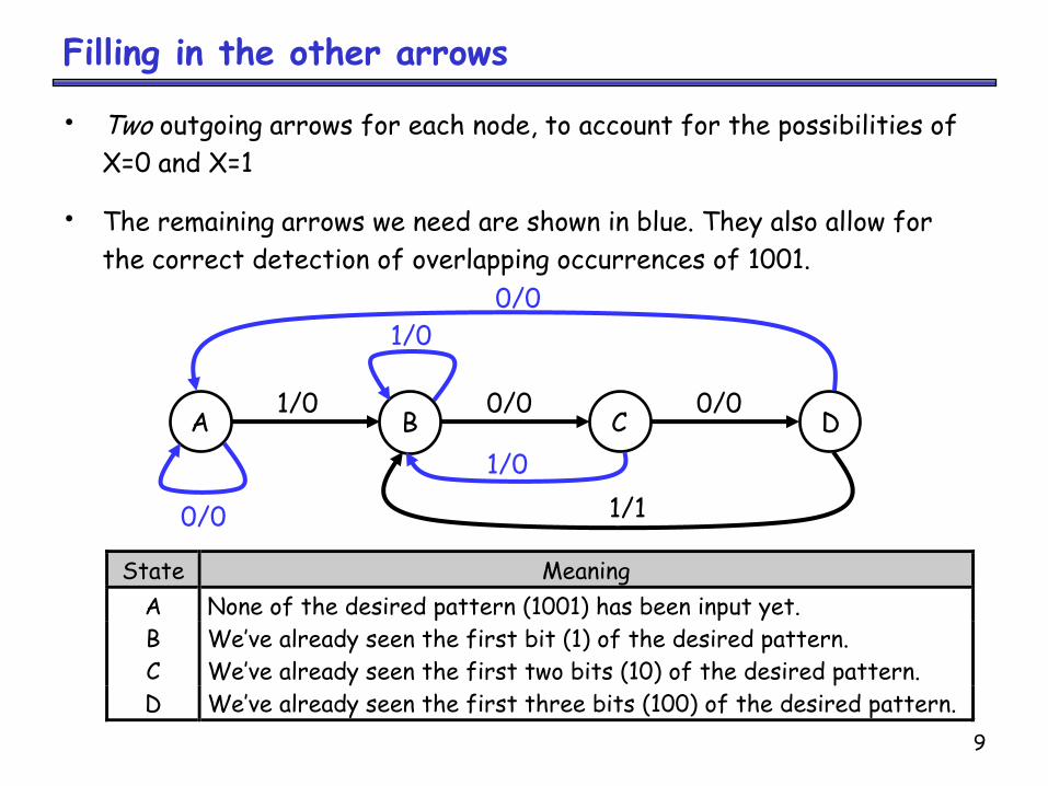
Filling in the other arrows
• Two outgoing arrows for each node, to account for the possibilities of
X=0 and X=1
• The remaining arrows we need are shown in blue. They also allow for
the correct detection of overlapping occurrences of 1001.
A B C D1/0 0/0 0/0
1/1
0/0
0/0
1/0
1/0
State Meaning
A None of the desired pattern (1001) has been input yet.
B We’ve already seen the first bit (1) of the desired pattern.
C We’ve already seen the first two bits (10) of the desired pattern.
D We’ve already seen the first three bits (100) of the desired pattern.
10
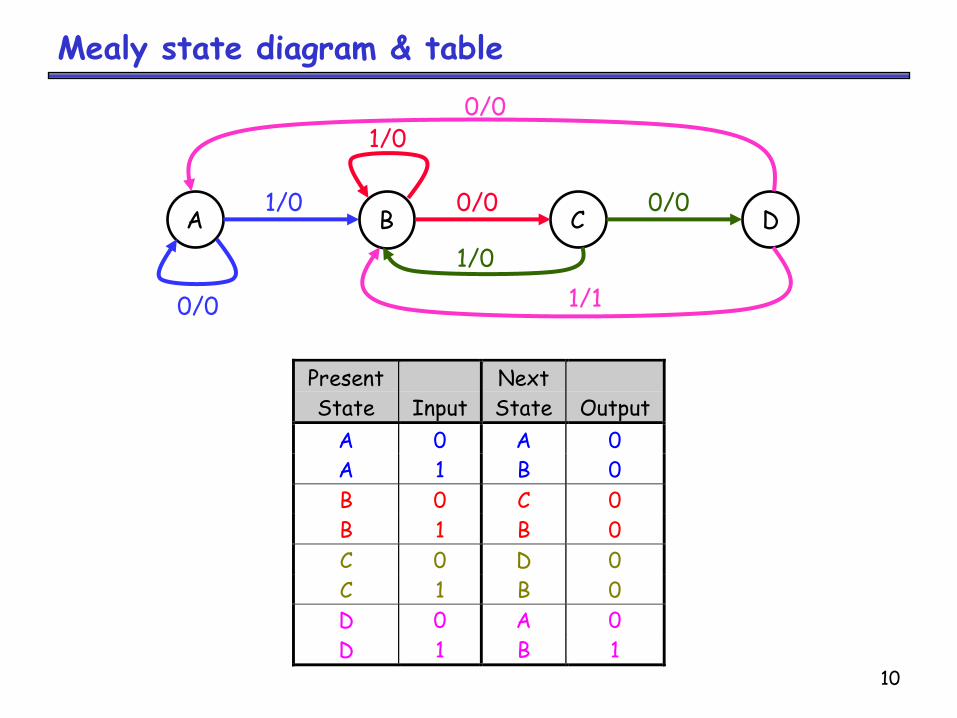
Mealy state diagram & table
A B C D1/0 0/0 0/0
1/1
0/0
0/0
1/0
1/0
Present
State Input
Next
State Output
A 0 A 0
A 1 B 0
B 0 C 0
B 1 B 0
C 0 D 0
C 1 B 0
D 0 A 0
D 1 B 1
11
Present
State Input
Next
State Output
A 0 A 0
A 1 B 0
B 0 C 0
B 1 B 0
C 0 D 0
C 1 B 0
D 0 A 0
D 1 B 1
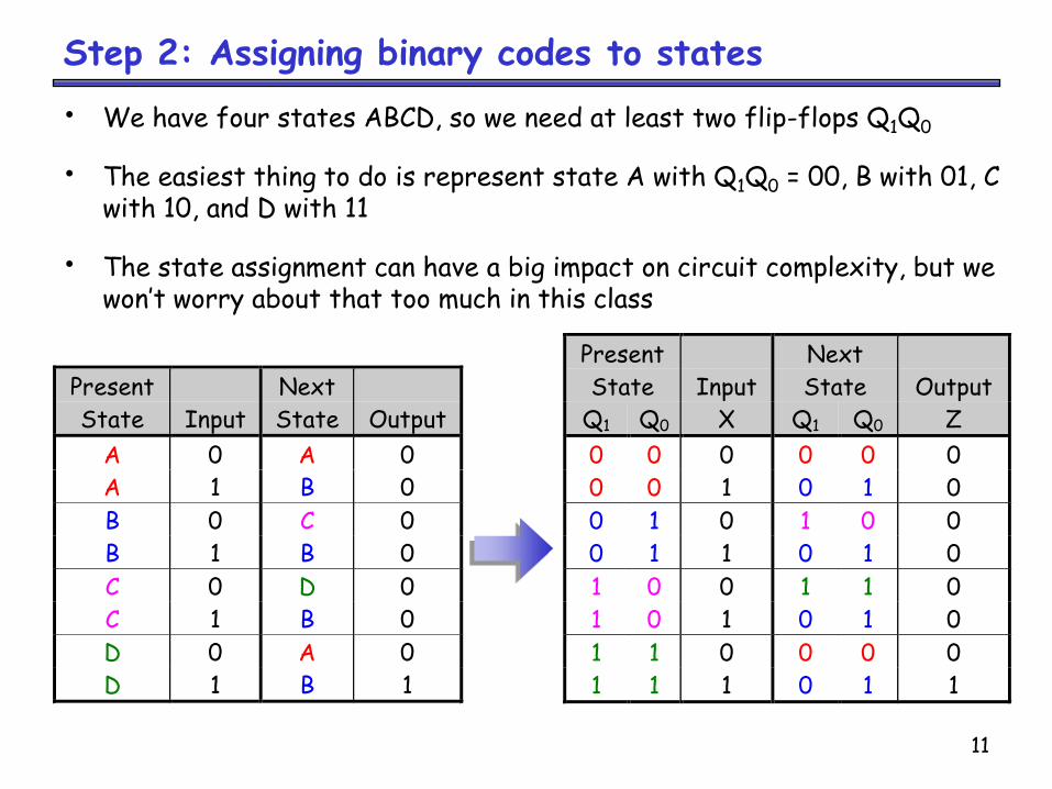
Step 2: Assigning binary codes to states
Present
State Input
Next
State Output
Q1 Q0 X Q1 Q0 Z
0 0 0 0 0 0
0 0 1 0 1 0
0 1 0 1 0 0
0 1 1 0 1 0
1 0 0 1 1 0
1 0 1 0 1 0
1 1 0 0 0 0
1 1 1 0 1 1
• We have four states ABCD, so we need at least two flip-flops Q1Q0
• The easiest thing to do is represent state A with Q1Q0 = 00, B with 01, C with 10, and D with 11
• The state assignment can have a big impact on circuit complexity, but we won’t worry about that too much in this class

12
Step 3: Finding flip-flop input values
Present
State Input
Next
State Flip flop inputs Output
Q1 Q0 X Q1 Q0 J1 K1 J0 K0 Z
0 0 0 0 0 0
0 0 1 0 1 0
0 1 0 1 0 0
0 1 1 0 1 0
1 0 0 1 1 0
1 0 1 0 1 0
1 1 0 0 0 0
1 1 1 0 1 1
• Next we have to figure out how to actually make the flip-flops change from their present state into the desired next state
• This depends on what kind of flip-flops you use!
• We’ll use two JKs. For each flip-flip Qi, look at its present and next states, and determine what the inputs Ji and Ki should be in order to make that state change.
13
Back to the example
Present
State Input
Next
State Flip flop inputs Output
Q1 Q0 X Q1 Q0 J1 K1 J0 K0 Z
0 0 0 0 0 0 x 0 x 0
0 0 1 0 1 0 x 1 x 0
0 1 0 1 0 1 x x 1 0
0 1 1 0 1 0 x x 0 0
1 0 0 1 1 x 0 1 x 0
1 0 1 0 1 x 1 1 x 0
1 1 0 0 0 x 1 x 1 0
1 1 1 0 1 x 1 x 0 1
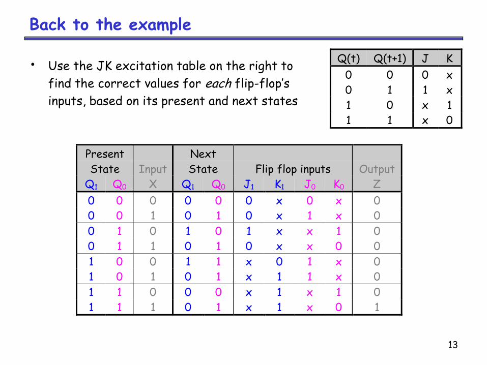
• Use the JK excitation table on the right to
find the correct values for each flip-flop’s
inputs, based on its present and next states
Q(t) Q(t+1) J K
0 0 0 x
0 1 1 x
1 0 x 1
1 1 x 0

14
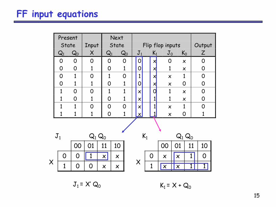
• Now you can make K-maps and find equations for each of the four flip-flop inputs, as well as for the output Z
• These equations are in terms of the present state and the inputs
• The advantage of using JK flip-flops is that there are many don’t care conditions, which can result in simpler MSP equations
Step 4: Find equations for the FF inputs and output
Present
State Input
Next
State Flip flop inputs Output
Q1 Q0 X Q1 Q0 J1 K1 J0 K0 Z
0 0 0 0 0 0 x 0 x 0
0 0 1 0 1 0 x 1 x 0
0 1 0 1 0 1 x x 1 0
0 1 1 0 1 0 x x 0 0
1 0 0 1 1 x 0 1 x 0
1 0 1 0 1 x 1 1 x 0
1 1 0 0 0 x 1 x 1 0
1 1 1 0 1 x 1 x 0 1
15
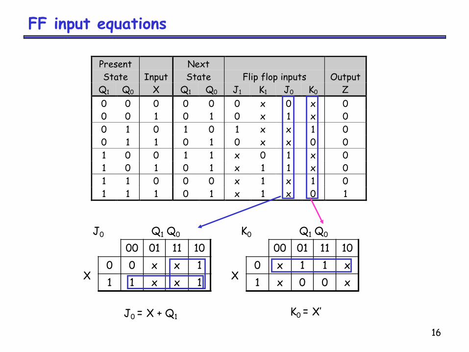
FF input equations
Present
State Input
Next
State Flip flop inputs Output
Q1 Q0 X Q1 Q0 J1 K1 J0 K0 Z
0 0 0 0 0 0 x 0 x 0
0 0 1 0 1 0 x 1 x 0
0 1 0 1 0 1 x x 1 0
0 1 1 0 1 0 x x 0 0
1 0 0 1 1 x 0 1 x 0
1 0 1 0 1 x 1 1 x 0
1 1 0 0 0 x 1 x 1 0
1 1 1 0 1 x 1 x 0 1
J1 Q1 Q0
00 01 11 10
X0 0 1 x x
1 0 0 x x
J1 = X’ Q0
K1 Q1 Q0
00 01 11 10
X0 x x 1 0
1 x x 1 1
K1 = X + Q0
16
FF input equations
Present
State Input
Next
State Flip flop inputs Output
Q1 Q0 X Q1 Q0 J1 K1 J0 K0 Z
0 0 0 0 0 0 x 0 x 0
0 0 1 0 1 0 x 1 x 0
0 1 0 1 0 1 x x 1 0
0 1 1 0 1 0 x x 0 0
1 0 0 1 1 x 0 1 x 0
1 0 1 0 1 x 1 1 x 0
1 1 0 0 0 x 1 x 1 0
1 1 1 0 1 x 1 x 0 1
J0 Q1 Q0
00 01 11 10
X0 0 x x 1
1 1 x x 1
J0 = X + Q1
K0 Q1 Q0
00 01 11 10
X0 x 1 1 x
1 x 0 0 x
K0 = X’
17
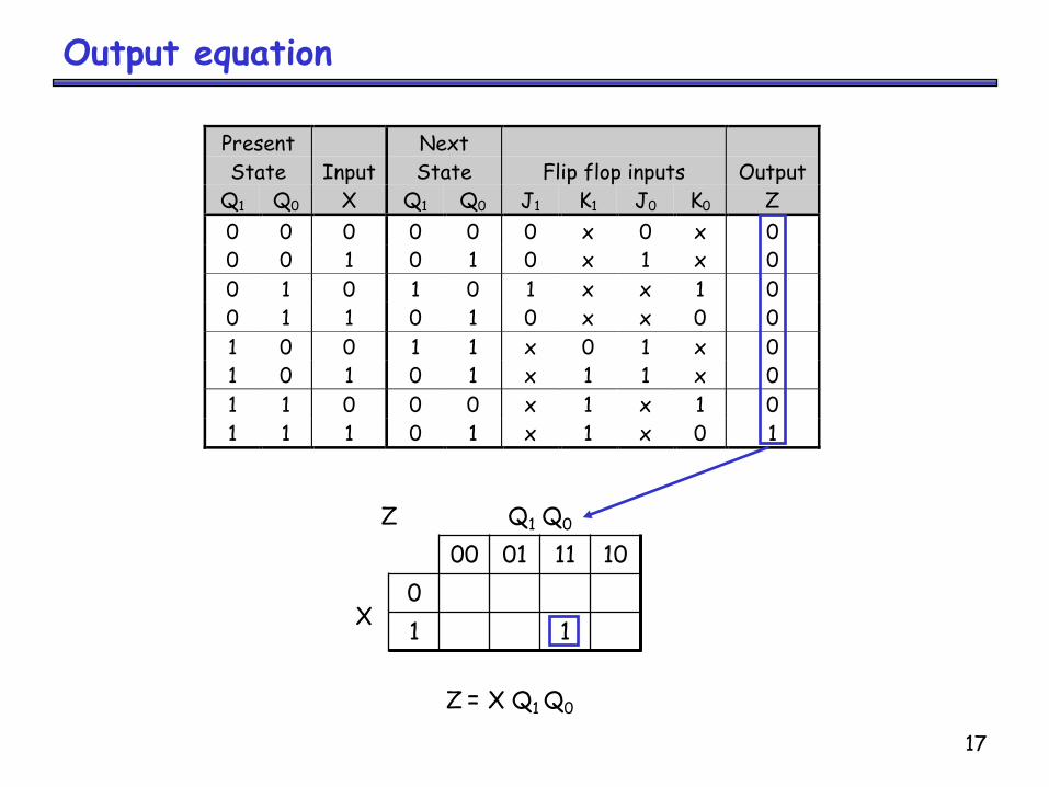
Output equation
Present
State Input
Next
State Flip flop inputs Output
Q1 Q0 X Q1 Q0 J1 K1 J0 K0 Z
0 0 0 0 0 0 x 0 x 0
0 0 1 0 1 0 x 1 x 0
0 1 0 1 0 1 x x 1 0
0 1 1 0 1 0 x x 0 0
1 0 0 1 1 x 0 1 x 0
1 0 1 0 1 x 1 1 x 0
1 1 0 0 0 x 1 x 1 0
1 1 1 0 1 x 1 x 0 1
Z Q1 Q0
00 01 11 10
X0
1 1
Z = X Q1 Q0

18
Step 5: The circuit
• Lastly, we use these simplified equations to build the completed circuit
J1 = X’ Q0
K1 = X + Q0
J0 = X + Q1
K0 = X’
Z = Q1Q0X

19
Building the same circuit with D flip-flops
• What if you want to build the circuit using D flip-flops instead?
• We already have the state table and state assignments, so we can just
start from Step 3, finding the flip-flop input values
• D flip-flops have only one input, so our table only needs two columns for
D1 and D0
Present
State Input
Next
State
Flip-flop
inputs Output
Q1 Q0 X Q1 Q0 D1 D0 Z
0 0 0 0 0 0
0 0 1 0 1 0
0 1 0 1 0 0
0 1 1 0 1 0
1 0 0 1 1 0
1 0 1 0 1 0
1 1 0 0 0 0
1 1 1 0 1 1

20
D flip-flop input values (Step 3)
• The D excitation table is pretty boring; set the D input to whatever the next state should be
• You don’t even need to show separate columns for D1 and D0; you can just use the Next State columns
Present
State Input
Next
State
Flip flop
inputs Output
Q1 Q0 X Q1 Q0 D1 D0 Z
0 0 0 0 0 0 0 0
0 0 1 0 1 0 1 0
0 1 0 1 0 1 0 0
0 1 1 0 1 0 1 0
1 0 0 1 1 1 1 0
1 0 1 0 1 0 1 0
1 1 0 0 0 0 0 0
1 1 1 0 1 0 1 1
Q(t) Q(t+1) D Operation
0 0 0 Reset
0 1 1 Set
1 0 0 Reset
1 1 1 Set

21
Finding equations (Step 4)
Present
State Input
Next
State
Flip flop
inputs Output
Q1 Q0 X Q1 Q0 D1 D0 Z
0 0 0 0 0 0 0 0
0 0 1 0 1 0 1 0
0 1 0 1 0 1 0 0
0 1 1 0 1 0 1 0
1 0 0 1 1 1 1 0
1 0 1 0 1 0 1 0
1 1 0 0 0 0 0 0
1 1 1 0 1 0 1 1
D1 Q1 Q0
00 01 11 10
X0 1 1
1
D1 = Q1 Q0’ X’ + Q1’ Q0 X’
D0 Q1 Q0
00 01 11 10
X0 1
1 1 1 1 1
D0 = X + Q1 Q0’
Z Q1 Q0
00 01 11 10
X0
1 1
Z = X Q1 Q0

22
Building the circuit (Step 5)

Mixed Flip Flops
23
Present
State
Input
Next
State
Flip flop inputs
Output
Q1 Q0 X Q1 Q0 J1 K1 T0 Z
0 0 0 0 0 0 x 0 0
0 0 1 0 1 0 x 1 0
0 1 0 1 0 1 x 1 0
0 1 1 0 1 0 x 0 0
1 0 0 1 1 x 0 1 0
1 0 1 0 1 x 1 1 0
1 1 0 0 0 x 1 0 0
1 1 1 0 1 x 1 0 1
T0 Q1 Q0
00 01 11 10
X0 0 1 0 1
1 1 0 0 1
24
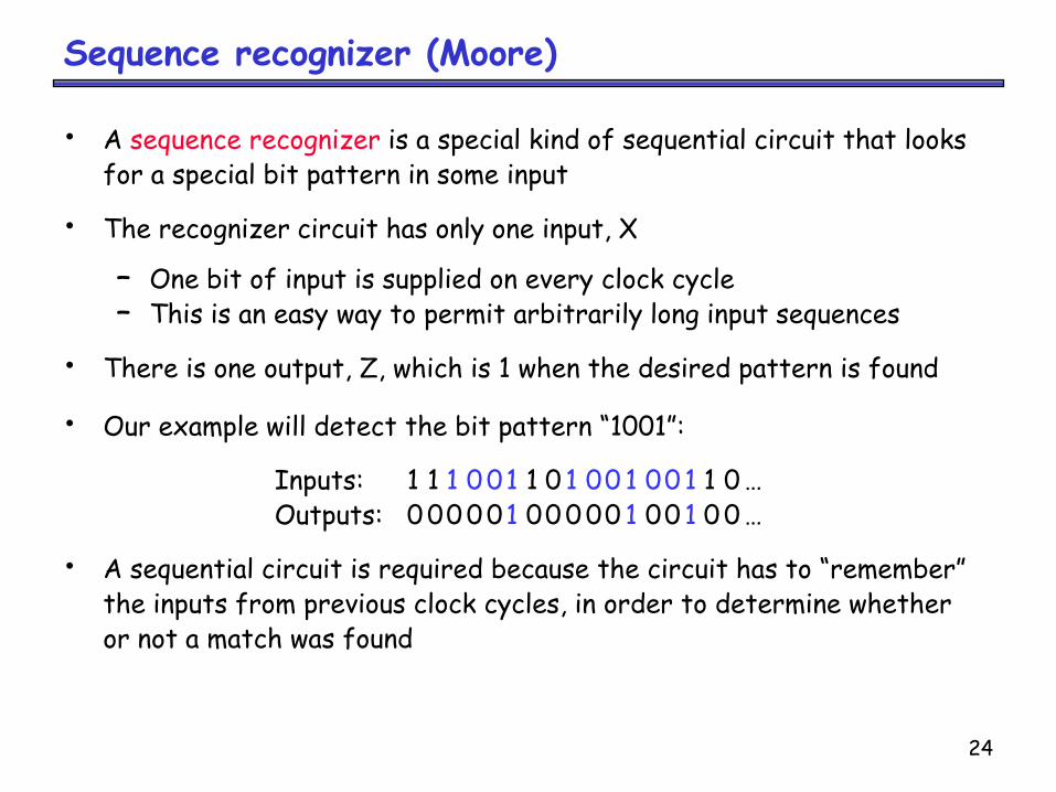
Sequence recognizer (Moore)
• A sequence recognizer is a special kind of sequential circuit that looks for a special bit pattern in some input
• The recognizer circuit has only one input, X
– One bit of input is supplied on every clock cycle– This is an easy way to permit arbitrarily long input sequences
• There is one output, Z, which is 1 when the desired pattern is found
• Our example will detect the bit pattern ―1001‖:
Inputs: 1 1 1 0 01 1 0 1 00 1 00 1 1 0 … Outputs: 0 00 0 01 00 0 00 1 00 1 0 0 …
• A sequential circuit is required because the circuit has to ―remember‖ the inputs from previous clock cycles, in order to determine whether or not a match was found

25
Moore state diagram & table
A/0 B/0 C/0 D/01 0 0
0
0
1
1
E/11
01
Present
State Input
Next
State Output
A 0 A 0
A 1 B 0
B 0 C 0
B 1 B 0
C 0 D 0
C 1 B 0
D 0 A 0D 1 E 0E 0 C 1E 1 B 1
Z Q2 Q1
00 01 11 10
Q0
0
1 1
A: 000 D: 100B: 001 E: 101C: 010
Z= Q2 Q1’ Q0