saurashtra universityetheses.saurashtrauniversity.edu/1052/1/pandya_dhiren_d...a copy can be...
TRANSCRIPT
Saurashtra University Re – Accredited Grade ‘B’ by NAAC (CGPA 2.93)
Pandya, Dhiren D., 2008, " Synthesis, Characterization and Studies on Some
Mixed Oxide Systems ", thesis PhD, Saurashtra University
http://etheses.saurashtrauniversity.edu/1052
Copyright and moral rights for this thesis are retained by the author
A copy can be downloaded for personal non-commercial research or study,
without prior permission or charge.
This thesis cannot be reproduced or quoted extensively from without first
obtaining permission in writing from the Author.
The content must not be changed in any way or sold commercially in any
format or medium without the formal permission of the Author
When referring to this work, full bibliographic details including the author, title,
awarding institution and date of the thesis must be given.
Saurashtra University Theses Service
http://etheses.saurashtrauniversity.edu
© The Author

Synthesis, Characterization and Studies on
Some Mixed Oxide Systems
A Ph.D. Thesis Submitted to
Saurashtra University, Rajkot, India
By
Dhiren Dinkarrai Pandya
Research Guide
Dr. N. A. Shah
Ph.D. Thesis Dhiren D Pandya July 2008

SYNTHESIS, CHARACTERIZATION AND STUDIES
ON SOME MIXED OXIDE SYSTEMS
THESIS
Submitted to
Saurashtra University, Rajkot, India
For the Degree of
Doctor of Philosophy
In Science
In the subject of Physics By
DHIREN DINKARRAI PANDYA
Under the supervision of
Dr. Nikesh A. Shah Assistant Professor
Department of Electronics
Saurashtra University
Rajkot -360 005
Gujarat-INDIA
July-2008

STATEMENT UNDER O. Ph. D. 7 OF THE SAURASHTRA UNIVERSITY
This is certified that the work presented in the thesis is my own
work, carried out under the supervision of Dr. N. A. Shah and leads to
some important contributions in Physics supported by necessary
references.
Dhiren D. Pandya (Research Student)
This is to certify that the work submitted for Ph.D. degree in
Physics to Saurashtra University, Rajkot by Mr. Dhiren D. Pandya has
been the result of more than three years of work under my supervision
and is a good contribution in the field of Solid State Physics and Materials
Science.
Dr. N. A. Shah
(Research Guide) Assistant Professor
Department of Electronics Saurashtra University
Rajkot

This thesis is dedicated to
My beloved Parents and FamilyMy beloved Parents and FamilyMy beloved Parents and FamilyMy beloved Parents and Family
Acknowledgements
“I am the source of all spiritual and material worlds. Everything emanates from Me.
The wise who perfectly know this engage in My devotional service and worship Me with
all their hearts.” Lord Krishna
First of all, I wish to give my sincere thanks to my Ph.D guide Dr. NIKESH A.
SHAH, for his consistent support and encouragement. It gives me massive pleasure to
express my deep sense of regards toward him for his valuable guidance throughout the
path of my research and life. Working with him, has definitely helped me to mature, both,
as a research student and as well as administrative person.
A very special thank-you goes to Prof. D. G.KUBERKAR for inspiration, support
and for being so generous with his time and knowledge. I have benefited greatly over the
years from his help, suggestion and backing. Without his enthusiasm and guidance, in
this dissertation would never have been completed.
Specially, I am thankful to Dr. Chetan M. Thaker, for his everlasting encourage
and for providing me moral support during this work.
I am also very grateful to, Dr. Jaysukh Markna, who has taken care of the fruitful
teamwork, discussion and painstaking computational work.
My sincere regards to Heads of the Department of Electronics and Physics,
Saurashtra University, for providing me the departmental facilities. I also wish to extend
my acknowledgements to all the faculty members of the Departments for their moral
support.
I would like to thank, Dr. J. A. Bhalodia, Dr. M. N. Jivani, Dr. K. P. Thummer
for the moral support during this work.
I am thankful to UGC-DAE CSR - Indore , T.I.F.R - Mumbai, IUAC - New Delhi
and RRCAT – Indore for experimental and characterization facilities during course of
research work.
I am thankful to our honorable Vice-Chancellor, Dr. K. P. Joshipura , honorable
Pro. Vice-Chacellor, Mr. Kalpakbhai Trivedi, The Registrar, my colleagues and staff
members of Saurashtra University.

It is a moment to remember my friends Dr. Bhavin Kothari, Dr.Bhadrayu, Mr.
Aswin, Dr. Yogesh, Dr.Denish, Mr. Shailesh, Mr. Rajesh, Mr. Navnit and Mr. Jayesh,
for providing a friendly and relaxing environment during my research work.
I also thank my lab.friends Dr. Rohini Parmar, Mr. Prashant, Mr. Piyush, Ms.
Rujuta, Mr. Jayesh, Mr. Dalsania, Mr.Bharat, Ms.Uma and Mr.Tulshi for their friendly
cooperation and help in this endeavor.
It is a great moment to remember my family for their unrelenting efforts for my
education since my childhood. My father Shri. Dinkarrai J. Pandya and Mother Smt.
Jyotiben D. Pandya have always supported endlessly for my higher education. I am
indebted to my parents for their unquestioning support and love. It is time to
acknowledge My brother Mr. Chandrakant D. Pandya and bhabhi Mrs. Ila C. Pandya,
my sisters, Mrs. Arunaben and Jijaji Mr. Dhirajlal, Mrs.Giraben and Mr.Yogeshkumar,
Mrs.Truptiben and Mr.Vallabhkumar for their endless love and supports .
I thank my father, mother and brother -in-law Shri. Jayantbhai, Smt. Sarojben
and Mr. Vipul Purohit for their moral support during the course of work.
Finally, I would like to thank my wife, MRS. KIRTIDA D.PANDYA and my loving
daughters JAYATI and PRAKRUTI for their continuous love and support.
July-2008 Dhiren D. Pandya

SCOPE OF FUTUTE RESEARCH ON MANGANITES
There are several issues listed below which needs further attention of the
condensed matter physicists.
There is need of understanding the cause for low temperature minima in
resistivity of manganites. Is it size or nano-cluster dependent?
Growth of different phase in manganite film for spintronics application.
Various thin films structures of manganites should be grown and tested for field
and temperature sensing applications at room temperature under low applied
fields.
The role of mixed phase and stabilization of charge and orbital ordering in
manganite is still open questions.
The presence of glassy state in some manganites similar to standard spin glass
behaviour has to be explored in detail and whether phase separation phenomenon
is responsible for such a behavior has to be studied.
Annealing effect in the thin film due to irradiation is interesting topic as research
point of view.

Preface
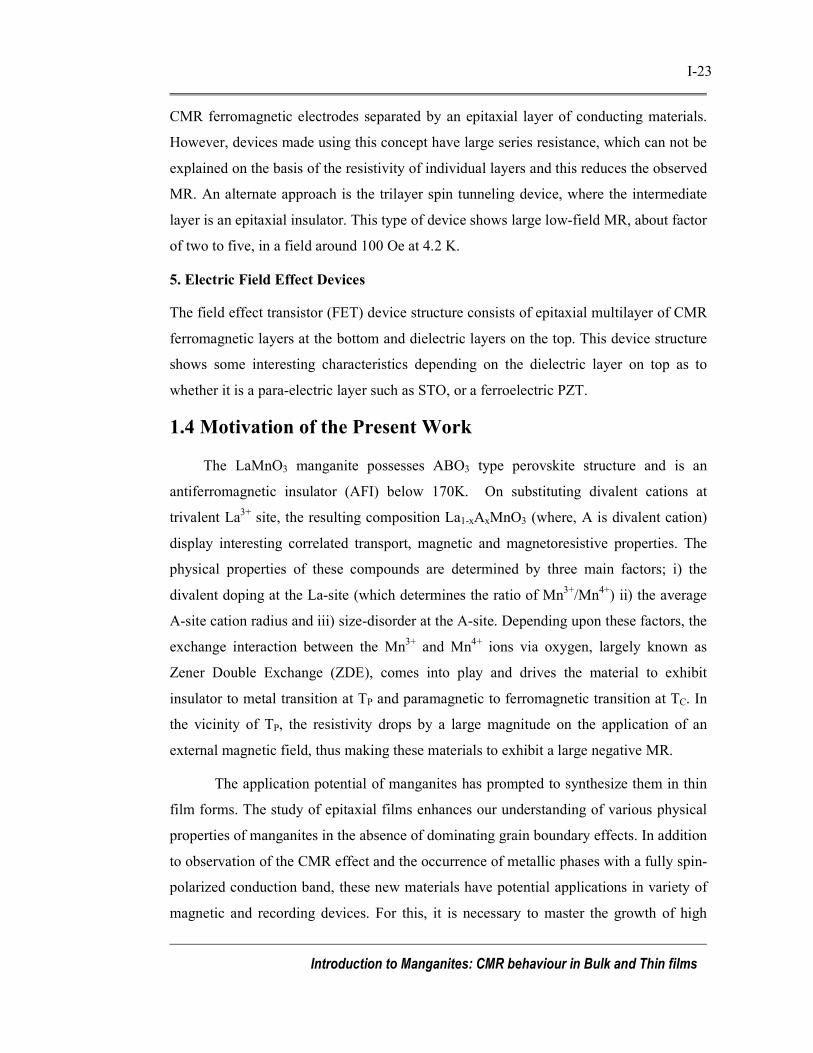
The LaMnO3 manganite compound possesses ABO3 type perovskite structure and is
an antiferromagnetic insulator (AFI) below 170 K. On substituting divalent cations at
trivalent cation, La3+, the resulting compositions La1- xAxMnO3 (where, A is divalent cation)
display interesting correlated transport, magnetic and magnetoresistive properties. The
physical properties of these compounds are determined by three main factors; i) the divalent
doping (substitution) at the La-site (which determines the ratio of Mn3+/Mn
4+) ii) the average
A-site cation radius and iii) size-disorder at the A-site. Depending upon these factors, the
exchange interaction between the Mn3+ and Mn
4+ ions via oxygen, largely known as Zener
Double Exchange (ZDE), comes into play and drives the material to exhibit insulator to metal
transition at TP and paramagnetic to ferromagnetic transition at TC. In the vicinity of TP, the
resistivity drops by large magnitude on the application of an external magnetic field, thus
making these materials to display a large negative MR.
The application potential of manganites has prompted the synthesis of these materials
in thin film forms. The study of epitaxial films enhances our understanding of various
physical properties of manganites in the absence of dominating grain boundary effects. In
addition to observation of the CMR effect and the occurrence of metallic phases with a fully
spin-polarized conduction band, these new manganite materials have potential applications in
varity of magnetic and recording devices. For this, it is necessary to master the growth of high
quality thin films with well-controlled and tailored properties. Progress in the growth of
epitaxial thin films opened the way to the applications of magnetic oxide materials in devices.
All the bulk materials in the present work were synthesized using solid state reaction
route at Department of Physics/Electronics, Saurashtra University, Rajkot, India. Thin films
were deposited using the Pulsed Laser Deposition technique. Most of the experimental work
has been performed in collaboration with Tata Institute of Fundamental Research (TIFR),
Mumbai, Raja Ramana Centre for Advance Technology (RRCAT), Indore and Inter-
University Accelerate Centre (IUAC), New Delhi, India.

Index
Chapter – 1
Introduction to manganite materials
1.1 Over view of CMR materials I-1
A) Background I-1
B) Magnetoresistance I-2
C) Type of magnetoresistance I-2
D) Structural properties I-7
E) Electronic transport properties I-10
F) Magnetic Properties I-11
1.2 Manganite thin films I-14
A) Background I-15
B) Grain boundary effect I-16
C) Strain effect I-17
D) Dead Layer I-20
1.3 Applications of magnetoresistive materials I-21
1.4 Motivation of the present work I-23
Reference I-26
Chapter – 2 Experimental techniques of characterization used
2.1 Synthesis Methods II-1
2.1.1 Ceramic method II-1
2.1.2 Different Techniques to grow thin films II-2
A) Pulse Laser Deposition. (PLD) II-2
B) Ion Beam Sputtering II-3
C) Molecular Beam Epitaxy (MBE) II-4
D) Chemical Solution Deposition (CSD) II-6

2.2 Structural Study II-7
2.3 Surface Morphology II-10
2.4 Electronic Transport and Magnetoresistive Properties II-16
2.4.1 D.C. four-probe method II-16
2.4.2 MR measurements (Low field and High field) II-19
2.5 Magnetic Susceptibility and Magnetization Measurements II-19
2.5.1 D.C. magnetization II-19
2.5.2 A.C susceptibility II-21
References II-23
Chapter – 3
Thickness dependent irradiation studies on La0.7Ca0.3MnO3/LAO
manganite thin film
3.1 Introduction III-1
3.2 Structural study and surface morphology III-3
3.2.1 Structural study III-3
3.2.2 SRIM calculation and Animation III-6
3.2.3 Surface Morphology III-7
3.3 Electronic transport properties III-9
3.4 Irradiation effects on the temperature sensitivity III-17
3.5 Magnetotransport properties III-19
3.6 Conclusion III-24
References III-26

Chapter – 4 Size disorder effect on the low temperature minima and
temperature sensitivity of (La0.5Pr0.2)(Ca0.3-xBax)MnO3
(0.05≤x≤0.3) manganite series.
4.1 Introduction IV-1
4.2 Structural studies IV-2
4.3 Electronic transport properties IV-6
4.3.1 Low temperature resistivity studies IV-9
4.3.2 Size disorder effects IV-15
4.4 Temperature sensitivity (TCR) study IV-24
4.5 Conclusion IV-28
References IV-30
Chapter – 5
Studies on Chemical Solution Deposited (CSD)
La0.8-XPr0.2SrxMnO3 (X=0.1,0.2,0.3) manganite series.
5.1 Introduction V-1
5.1.1 Preparation method V-2
5.2 Structural studies V-4
5.3 Surface morphology using AFM V-6
5.4 Electronic transport and Temperature sensitivity
Studies V-8
5.5 Magnetotransport Properties V-10
5.6 Conclusion V-13

References V-15
Scope of future research on manganites
List of Publications

Chapter - 1

Introduction to Manganites: CMR behaviour in Bulk and Thin films
I-1
1.1. Overview of CMR materials.
More recently, attention has been focused on certain class of manganese oxides
and perovskite structured manganites. Although these materials have been studied for
several years, the current burst of activity was stimulated due to the report by Helmholt
et al and Jin et al on the observation of extremly large ‘‘colossal’’ megnetoresistance in
these compounds[1, 2]. Magnetoresistance, the variation of electrical resistance with
magnetic field, is crucial to several areas of technology, such as magnetic data storage,
and much of the impetus for the present interest in the manganites systems from the
possible utility of their magnetoresistive properties [3, 4]. Whether the manganite
perovskites currently under consideration will prove technologically useful is still far
from clear. But the observation of colossal magnetoresistance has stimulated a
considerable amount of work aimed mainly at understanding and improving their
magnetoresistive properties, and at examining other related classes of transition-metal
oxides (such as spinels, pyrochlores and magnetites) which display similar behaviour and
may have more technologically convenient properties [5, 6, 7].
The manganites are interesting compounds having exciting properties from both
the basic research as well as from technological point of view. As the technology
pursued with this material requires film growth, extensive studies have been made on
material synthesis, structural and physical characterization and device fabrication[8, 9].
A) Background
The mixed valent manganese oxides possess rich and complex physics related to
the importance of electron-lattice and electron-electron interactions[10, 11]. The
structural, magnetic and transport properties of these compounds are intricately related.
In addition, the Colossal Magneto Resistance (CMR) effect exhibited by manganites and
the occurrence of metallic phases with a fully spin-polarized conduction band are
promising for potential applications. Various technologically important applications of
manganites require their high quality thin films having well-controlled & tailored
properties. Progress in the growth of epitaxial thin films opens a way to all oxide or
oxide-metal devices [12, 13].
Introduction to Manganites: CMR behaviour in Bulk and Thin films
I-2
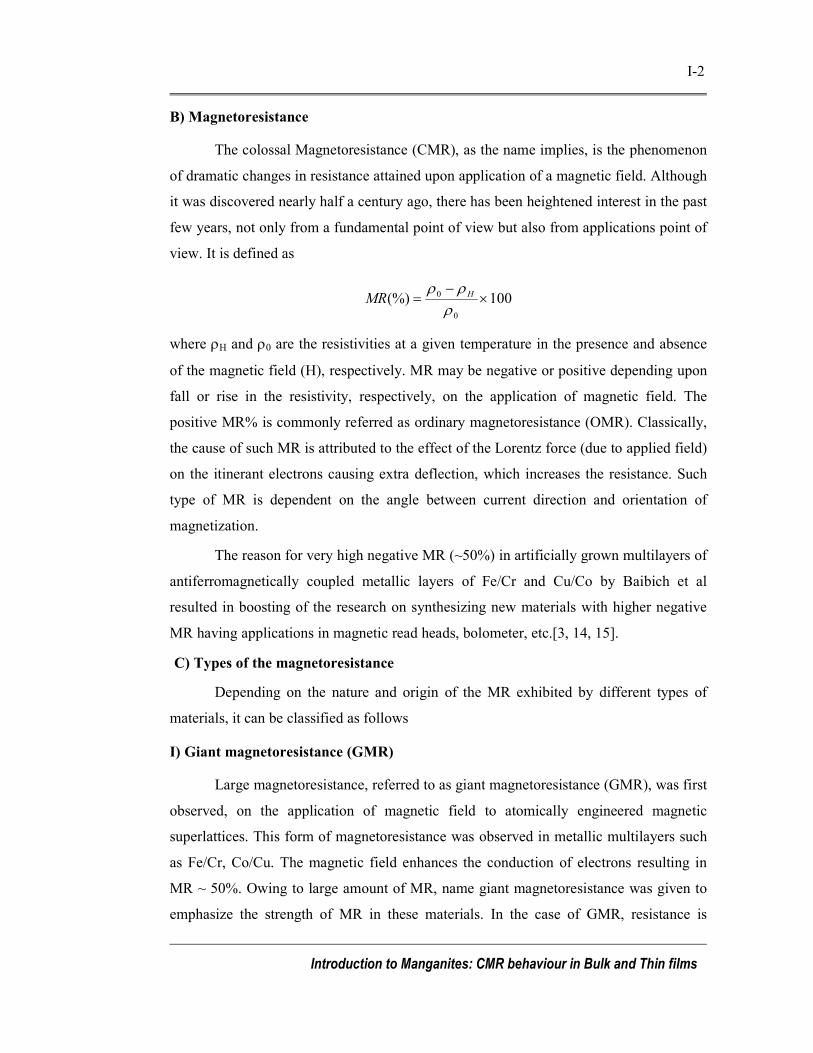
B) Magnetoresistance
The colossal Magnetoresistance (CMR), as the name implies, is the phenomenon
of dramatic changes in resistance attained upon application of a magnetic field. Although
it was discovered nearly half a century ago, there has been heightened interest in the past
few years, not only from a fundamental point of view but also from applications point of
view. It is defined as
100(%)0
0 ×−
=ρρρ HMR
where ρH and ρ0 are the resistivities at a given temperature in the presence and absence
of the magnetic field (H), respectively. MR may be negative or positive depending upon
fall or rise in the resistivity, respectively, on the application of magnetic field. The
positive MR% is commonly referred as ordinary magnetoresistance (OMR). Classically,
the cause of such MR is attributed to the effect of the Lorentz force (due to applied field)
on the itinerant electrons causing extra deflection, which increases the resistance. Such
type of MR is dependent on the angle between current direction and orientation of
magnetization.
The reason for very high negative MR (~50%) in artificially grown multilayers of
antiferromagnetically coupled metallic layers of Fe/Cr and Cu/Co by Baibich et al
resulted in boosting of the research on synthesizing new materials with higher negative
MR having applications in magnetic read heads, bolometer, etc.[3, 14, 15].
C) Types of the magnetoresistance
Depending on the nature and origin of the MR exhibited by different types of
materials, it can be classified as follows
I) Giant magnetoresistance (GMR)
Large magnetoresistance, referred to as giant magnetoresistance (GMR), was first
observed, on the application of magnetic field to atomically engineered magnetic
superlattices. This form of magnetoresistance was observed in metallic multilayers such
as Fe/Cr, Co/Cu. The magnetic field enhances the conduction of electrons resulting in
MR ~ 50%. Owing to large amount of MR, name giant magnetoresistance was given to
emphasize the strength of MR in these materials. In the case of GMR, resistance is

Introduction to Manganites: CMR behaviour in Bulk and Thin films
I-3
dependent on the direction of the magnetization because electrons have different
scattering probabilities in the presence of parallel and anti- parallel magnetization
directions. The GMR is usually defined as
AP
APP
R
RRGMR
−=
where, RAP and RP the resistances of the stack of layers with anti-parallel (AP) and
parallel (P) state of the magnetizations, respectively.
Figure:1.1: Magnetoresistance of Cr/Fe multilayers measured at 4.2 K
(reproducedfrom the reference 14)
GMR effect occurs in materials consisting of thin alternating layers of
ferromagnetic and non-magnetic metals, and the effect arises as a result of spin
dependent transport within the system. The resistivity of the system depends on the
relative alignment (parallel or antiparallel) of the moments of the ferromagnetic layers.
Layers with parallel magnetic moments have less scattering at the interfaces, longer

Introduction to Manganites: CMR behaviour in Bulk and Thin films
I-4
mean free paths and lower resistance. Layers with antiparallel magnetic moments have
more scattering at the interfaces, shorter mean free paths and higher resistance.
II). Anisotropic Magnetoresistance (AMR)
In this type of magnetoresistance, change in the resistance is related to the
variation in the magnetization of the ferromagnetic film. The AMR can be expresses as
⊥
⊥∏ −=R
RRAMR
where, R∏ and R⊥ are resistances with the field applied parallel and perpendicular to the
sample, respectively. In the case of AMR, the resistance is anisotropic and depends on
the orientation of the magnetization with respect to the current. The origin of the AMR
effect lies in the spin-orbit coupling and the splitting of the d-bands in ferromagnetic
metals.
III). Tunneling Magnetoresistance (TMR)
Tunneling magnetoresistance phenomenon is observed in the tunneling junction
of the two ferromagnetic layers which are separated by an insulating barrier. Similar to
other MR effect, in the TMR, considerable change in resistance is observed when the
relative orientation of the two magnetic layers changes from anti parallel to parallel. The
relative change in the resistance, TMR, is quantified by the equation
AP
APP
I
IITMR
−=
where, IP is the current when both the ferromagnetic layers have parallel magnetizations
while IAP is the current when one ferromagnetic layer has a parallel magnetization and
another layer has anti-parallel magnetization.
IV). Colossal magnetoresistance (CMR)
In 1993, R. Von Helmolt et al discovered that La2/3Ba1/3MnO3 exhibit huge
magnetoresistance around room temperature with many interesting interrelated
phenomena[1]. The strength of MR observed in many similar polycrystalline compounds
as high as 90% under a few Tesla led the scientists to coin a new term called “colossal

Introduction to Manganites: CMR behaviour in Bulk and Thin films
I-5
magneto resistance (CMR)”[16]. The CMR can be determined from the ratio of a change
in the resistivity under the magnetic field, which is expressed as,
1000
0 ×−
=ρρρ HCMR
The observation of CMR effect in the metallic oxides induced interest in
researchers to exploit these compounds for the possible applications. Unlike artificially
grown metallic multilayers where extrinsic factors such as the interface between the two
layers, roughness and grain structure govern the magnetoresistance, these compounds
have ionic size dependent intrinsic properties responsible for colossal magnetoresistance.
These intrinsic factors in this ABO3 type of perovskite, with limits on the size of A and B
site cations for occurrence of CMR effect, can be controlled by the compositional
changes in the compound. The interplay with size of the cations to alter the MR
properties of the manganite perovskites evolved plenty of scope in further research in
related materials.
The basic manganite oxide ReMnO3 where Re = La, Pr, Nd is a paramagnetic
insulator at all the temperatures, however, exhibits paramagnetic to antiferromagnetic
transition around 150 K. The optimum divalent cation doping at A site drives the
resulting material to exhibit properties such as coincident insulator – metal (I-M)
transition and paramagnetic – ferromagnetic (PM-FM) transition. The maximum CMR
effect occurs around this coincident transition temperature. Re and Mn ions exist in +3
oxidation state in ReMnO3 perovskite. The divalent Ca2+, Sr2+, Ba2+ and Pb2+ cations
substitution at A site drives Mn at B site to exist in mixed valent (Mn3+/Mn4+) state
which is responsible for most of the transport and magnetic properties of the perovskite.
Due this mixed valent state of Mn, these compounds are also called as mixed valent
manganite oxides. The conduction in these oxides is explained by a phenomenon
discovered by C. Zener in 1951 called as “Zener-Double Exchange (ZDE)”[17]. All the
transport mechanisms such as ZDE occur through Mn – O – Mn network, where as A
cation is not directly involved in any conduction mechanism. The Mn4+ valence state is
formed due to substitution of same amount of divalent cation at A-site. The octahedral
crystal field of oxygen octahedra (MnO6) lifts the five fold degenerate Mn 3d orbitals
into three lower energy t2g (dxy, dyz & dzx) and two higher energy eg (dx2-y2, dz
2) orbitals.

Introduction to Manganites: CMR behaviour in Bulk and Thin films
I-6
Further, the octahedral crystal field split the two eg orbitals into two energy levels which
is called Jahn – Teller splitting that cause orbital ordering of MnO6 octahedra along the
planes where last filled electron lies just at the fermi level. The hole doping removes
Jahn – Teller distortion along the planes. At Mn3+- O2- - Mn4+ coupling, the last eg
electron in Mn3+ feels a net energy difference and it becomes delocalized via O2- to Mn4+.
This process of Zener Double exchange accounts for both the metallic and ferromagnetic
character of the material below a certain temperature called transition temperature. The
phenomenon of ZDE is possible only if the spins of the alternate manganese ions are
aligned parallel.
The A site cation in ABO3 type perovskite manganite does not involve in any
conduction mechanism but has its ionic size effect on the transport and magnetic
properties. A parameter called as “Goldschimdt tolerance factor” relates the different site
ionic radii to the transition temperature[5].
Figure:1.2: Schematic crystal structure of the manganite perovskite.
The structure of the manganite is governed by the tolerance factor
t = (rA +rO)/√√√√2 (rB +rO).
where, <rA> = average A site cation radius
<rB> = average B site cation radius
<rO> = radius of oxygen anion
The perovskite structure is stable in the range 0.89 < t < 1.02, t = 1 corresponding
to the perfect cubic closely packed structure. Generally, t differs appreciably from 1 and

Introduction to Manganites: CMR behaviour in Bulk and Thin films
I-7
the manganites have, at least, at low temperature, a lower rhombohedral symmetry or
orthorhombic structure. This is illustrated by the orthorhombic structure of LaMnO3 (Fig.
1.3), which is the parent compound of the most of the manganites studied for potential
application by partial substitution of La by Ca and Sr.
The discovery of CMR in manganites and its relation to various electronic and
magnetic properties rejuvenated the research interest in similar compounds. Since
manganites appear promising candidates, both from basic research and applications point
of view, a major fraction of materials scientists have contributed to the better
understanding of these materials. This thesis is devoted to the understanding of various
physical properties of complex manganite systems and some efforts to evaluate the
application potentiality of these compounds.
D) Structural Properties
I). Crystallographic and Electronic Structure
The structure of the Re1-XMXMnO3 oxides is close to that of the cubic perovskite
(Fig.1.3). The large sized Re-trivalent ions and M-divalent ions occupy the A site with
12 - fold oxygen coordination. The smaller Mn ions in the Mn+3 – Mn+4 mixed valent
state are located at the centre of an oxygen octahedron i.e. at the B-site with 6-fold
coordination. For the stoichiometric oxide, the proportions of Mn ions in the +3 & +4
valence states are respectively, 1-x and x.
Figure 1.3: Schematic view of the cubic perovskite structure. Crystallographic
structure of LaMnO3.

Introduction to Manganites: CMR behaviour in Bulk and Thin films
I-8
For an isolated 3d ion, five degenerate orbital states are available to the 3d
electrons with l = 2. In a crystal, the degeneracy is partly lifted by the crystal field. The
five d-orbitals are split by a cubic crystal field into three t2g orbitals and two eg orbitals.
For the MnO6 octahedron, the splitting between the lowest t2g level and the highest eg
level is ∆ ~ 1.5 eV (Fig.1.4). For the Mn3+ and Mn4+ ions, the intra-atomic correlations
ensure parallel alignment of the electron spins having corresponding exchange energy of
about 2.5 eV larger than the crystal field splitting ∆. Mn3+ is 3d4, t2g3↑ eg
↑ with S = 2
whereas Mn4+ is 3d3, t2g3↑ with S=3/2. Their respective magnetic moments are 4µB and
3µB, neglecting the small orbital contribution.
Figure 1.4: Field splitting of five-fold degenerate atomic 3d levels into lower t2g
(triplydegenerate) and higher eg (doubly degenerate) levels. Jahn-
Teller distortion of MnO6 octahedron further lifts each degeneracy
as shown in the figure.
In a crystal field of symmetry lower than cubic, the degeneracy of the eg and t2g
levels is lifted, as shown in the fig.1.4 for an axial elongation of the oxygen octahedron.
Although the energy of Mn4+ remains unchanged by such a distortion, the energy of
Mn+3 is lowered. Thus, Mn+3 has a marked tendency to distort its octahedral environment
in contrast to Mn+4. This Jahn – Teller distortion is rather effective in the lightly doped
manganites; i.e. with a large concentration, 1-x, of Mn+3 ions; the Jahn-Teller distortions
are not independent from one Mn+3 site to another (cooperative Jahn-Teller effect). This

Introduction to Manganites: CMR behaviour in Bulk and Thin films
I-9
is illustrated by the structure of LaMnO3 (Fig.1.3) in which the MnO6 octahedra are
strongly elongated within the ab plane in a regular way leading to a doubling of the unit
cell. On increasing the Mn+4 content, the Jahn-Teller distortions are reduced and the
stabilization of the 3z2-r2 eg orbital becomes less effective. Nevertheless, in a large
number of manganites, the eg orbitals of two types, 3z2-r2 and x2-y2 are not occupied by
the eg electrons of Mn3+ at random and an orbital order is achieved.
Double Exchange
Figure 1.5: Schematic view of the double exchange (DE) mechanism.
A peculiar and interesting case is that of Mn+3-O-Mn4+ for which the Mn ions can
exchange their valence by a simultaneous jump of the eg electron of Mn+3 on the
O p -orbital and from the O p-orbital to the empty eg orbital of Mn+4. This mechanism of
DE originally proposed by Zener ensures a strong ferromagnetic-type interaction [17].
As shown by Anderson and Hasegawa, the probability of the eg electron transfer from
Mn3+ to neighboring Mn4+ is toCOS(θ /2), θ being the angle between the Mn spins, in the
case of strong Hunds coupling (Fig.1.5)[18]. The process of electron transfer lifts the
degeneracy of the configurations Mn+3 - O - Mn+4 and Mn4+- O -Mn3+ leading to two
energy levels Et=0 ± toCOS(θ /2). The energy gain of the parallel spin configurations to
θ = 0, which maximizes t, with respect to the anti-parallel one θ =π, reveals the
ferromagnetic character of the DE interaction. However in the DE, angular dependence
of COS(θ /2) is quite different from COS(θ) of the usual exchange interaction. This
different angular dependence in conjunction with the competition between DE
ferromgmagnetism and superxchange anti-ferromagnetism is at the origin of the complex
magnetic phase diagram of manganites versus the doping level, x. In particular, canted
AF phases at small x were predicted early on by P. G. de Gennes[19].

Introduction to Manganites: CMR behaviour in Bulk and Thin films
I-10
E) Electronic Transport Properties
The simple manganites, such as La1-XMXMnO3 (M= Ca, Sr, Ba) with x = 1/3 with
strong DE exhibits a transition from high temperature paramagnetic (PM) semi-
conducting or insulating (I) phase to a low temperature FM phase.
I) Paramagnetic region
In the P phase, the electrical resistivity generally exhibits strong temperature
dependence. Different ρ(T) laws have been used in fitting experimental data, the most
popular ones being: (1) simple thermal activation law ρ = ρ∞ exp(E0/kBT) with a typical
gap value of ~ 0.1 eV (ii) hopping of adiabatic polarons ρ ~ T exp(E0/kBT); (iii) Mott
variable range-hopping (VRH), ρ = ρ∞ exp [(T0/T)1/4]. Each of these laws have some
physical origins, which is respectively (i) the existence of a pseudogap at the Fermi level
in the P phase (ii) the local lattice distortion accompanying the moving charge carrier
(Jahn-Teller polarons); (iii) the localization of the charge carriers by the magnetic
disorder. In a narrow range of temperature, it is practically impossible to discriminate
between these different ρ(T) laws [20].
II) Ferromagnetic region
At low temperature, the spontaneous alignment of the Mn spins below the Curie
temperature, TC, allows the delocalization of the eg electrons, leading to a low resistive
FM phase with ρ ≈ ρ0 + aT2 for T ≤ TC. This alignment of the Mn spins can be induced
for T ≥ TC, or reinforced for T ≤ TC, by applying an external magnetic field. The
maximum effect is obtained close to TC since the initial magnetic susceptibility diverges
as T →TC. Thus, these manganites have a rather large negative magnetoresistance, the so
–called CMR, which peaks at about TC. This phenomenon is observed in large number of
manganites. In general, since the resistivity of the P phase strongly increases on
decreasing T, whereas that of the FM phases decreases, the CMR becomes larger as TC
becomes smaller at least for a given doing level.
III) Effects of doping level and A-site cation size
The physical properties of perovskite-type manganites are determined by two
main parameters: the doing level, x = Mn4+/ (Mn3+ + Mn4+), and the average size of the
cation A, <rA>. A third relevant parameter is the degree of disorder at site A, defined by

Introduction to Manganites: CMR behaviour in Bulk and Thin films
I-11
∑ ><−= 222Aii rrxσ
[11]. An enormous number of experimental studies have been
performed to quantify these effects. In general, ferromagnetic DE is maximum around
x=1/3 and for <rA> ≈ 1.24 Å. The reduction of <rA> from this optimum value leads to an
increasing distortion of the crystallographic structure. The resulting reduction of the
Mn-O-Mn angle from 180º to a smaller value weakens the ferromagnetic DE and
increases the tendency to localize the charge carriers. This drastic effect of <rA> on the
resistivity, is exemplified by the phase diagram in fig.1.6 for x=0.3[21]. Figure 1.6 also
shows the phase diagram of two extreme cases of La1-xSrxMnO3 which is most FM
manganite and Pr1-xCaxMnO3 which displays large charge ordering (CO) effects.
Figure 1.6: Phase diagrams of temperature versus tolerance factor and average
radius of cation at A-site for Re0.7A0.3MnO3, single crystal
La1-xSrxMnO3 and Pr1-xCaxMnO3 system(reproduced from the
reference21, 22).
F) Magnetic properties
The magnetic properties of the manganites are governed by exchange interactions
between the Mn ion spins. These interactions are relatively large between two Mn spins
separated by an oxygen atom and are controlled by the overlap between the Mn
d-orbitals and the O p-orbitals. The corresponding superxchange interaction depends on
the orbital configuration following the rules of Goodenough & Kanamori[23]. Generally,
for Mn4+-O-Mn3+, the interaction is AF, whereas Mn3+-O-Mn4+, such as in LaMnO3
where both F and AF interactions coexist. The LaMnO3 end member was found to be
antiferromagnetic, with ferromagnetic planes that had alternating directions of

Introduction to Manganites: CMR behaviour in Bulk and Thin films
I-12
magnetization. The other end member CaMnO3 was also found to be antiferromagnetic
with each Mn+4 surrounded by the six closest neighbors having opposite spin. Other
doping levels gave different types of antiferromagnetic ordering but in the doping range
of x ≅ 0.3, the samples were ferromagnetic. Goodenough has explained the magnetic
structures for different doping levels in terms of different types of bonding, where some
bonds are ferromagnetic and others are antiferromagnetic or paramagnetic. This is
determined by the relative orientation of occupied and unoccupied orbitals of the Mn-O-
Mn pairs.
I) Charge and Orbital Ordering in Manganites
As shown in the fig. 1.6, upon doping, the manganites exhibit a wide varity of
ordered states, including ferromagnetic and charge-ordered (CO) phases. In these
compounds, there exist orbital degrees of freedom of the eg electrons in Mn3+ ions, and
orbital ordering can lower the electronic energy through the Jahn-Teller mechanism.
Therefore, charge and orbital-ordering effects are particularly pronounced in mixed
valent manganites. Some of the arrangements that have been identified are shown in
fig.1.7. At x=0, the A-type spin state is orbitally ordered as it appears in the fig. 1.7 (a).
Figure 1.7. (b) shows the related charge and orbital ordering scheme for x=0.5, where
there is same amount of Mn4+ and Mn+3 ions and the charge-exchange (CE) type
arrangement is formed. In La1/3Ca2/3MnO3, there are twice as many Mn4+(3d3) ions as
compared to the Mn3+(3d4) ions and the ordering of the diagonal rows of Mn4+ and Mn3+
ions plus the orientational ordering of the dz2 orbitals in Mn3+ gives rise to the stripe
pattern as shown in fig.1.7.(c)[24].
Figure 1.7 : The charge and orbital ordering configurations in the orthorhombic
basal plane for x= 0, ½, 2/3 of La1-xCaxMnO3. Open circles are Mn4+
and the lobes show the orbital ordering of the eg electrons of Mn3+

Introduction to Manganites: CMR behaviour in Bulk and Thin films
I-13
Figure 1.8: Spin, charge and orbital ordering pattern of CE antiferromagnetic
type observed for most of the x=1/2 manganites. The eg orbital
ordering on Mn3+ sites is also shown. The Mn
3+ sites are indicated by
closed circles.
Several other manganites exhibit CE- type CO-phase at x=0.5 as well. A sketch
of the complex orbital, charge and spin order is shown in figure 1.8. While the spins are
purely antiferromagnetic, the charge and orbital ordering occurs in alternate b-c planes,
giving rise to charge-stack order. This state can be easily destroyed by a magnetic field
in a first order transition [25]. Investigations on charge ordering have established the
intimate connection of the lattice distortion to CO. It is the lattice distortion associated
with orbital ordering that appears to localize the charge and initiate charge ordering.
Eventually, the Coulomb interaction wins over the kinetic energy of the electrons to form
long range CO state. The scale of the energy involved with CO as measured by the
charge-ordering gap is around 0.5-1 eV. This is similar to the unscreened bare nearest
neighbor Coulomb repulsion. This is also close to the approximate energy required to
create ~ 1 % orthorhombic distortion. It is likely that both the energy scales along with
magnetic exchange decides the energy scale of the charge-ordering gap.
II) Magneto transport Properties
High Field Magnetoresistance (HFMR)
In the ferromagnetic region, manganite sample shows metallic behaviour, i.e. a
positive temperature coefficient of the resistivity. Near the ferromagnetic transition, spin

Introduction to Manganites: CMR behaviour in Bulk and Thin films
I-14
disorder leads to a sharp increase in the resistivity. The application of an external
magnetic field results in to decrease in the resistivity, with the highest negative MR
occurring close to the magnetic transition temperature, which is indicated by peak in the
zero-field resistivity. The peak in the resistivity becomes smaller and shifts to higher
temperature with the field. This gives resistivity suppression in high field and MR known
as high field magnetoresistance.
Low Field Magnetoresistance (LFMR)
Presently large numbers of research groups are trying to achieve large, low field
RT MR in substituted rare earth manganites. The physical reason behind the observation
of low field magnetoresistance (LFMR), in the epitaxial and granular thin films (with
grain boundaries) as well as in the bulk sample is totally different[26]. The epitaxial film
shows almost zero MR, however, bulk material show much larger negative MR as
compared to the epitaxial thin films. This is one of the interesting aspects of transport in
these materials and needs detailed investigation. In bulk samples and granular thin films
having grain boundary effects, large LFMR at low temperature is exhibited due to the
intergrain tunneling in the magnetic domain.
1.2 Manganite thin films
Besides the discovery of the large RT MR, the renewed interest in manganites
has been propelled by another reason: the ability to synthesize high quality thin films as
single crystal forms of complex perovskite oxide materials. The emergence of epitaxial
metal oxide films has been one of the most attractive subjects of research of the
condensed matter community in the last decade, which was primarily stimulated by the
discovery of high-temperature superconductors (HTSC) and more recently by the
discovery of CMR effects in the manganite. Large Number of technique are available to
deposit the manganite thin film such as sputtering, molecular beam epitaxy (MBE),
Chemical Solution Deposition and metal-organic chemical vapor deposition (MOCVD),
but most popular technique is probably the pulsed-laser deposition (PLD). The
manganite oxides are highly sensitive to the strain effect, and this offers the possibility of
studying its influence upon various properties such as insulator-metal transition
temperature (TIM), Curie temperature (Tc), structure and microstructure/morphology.

Introduction to Manganites: CMR behaviour in Bulk and Thin films
I-15
This section will present a brief review of the experimental work done on the
manganite thin films in the past few years. Since it is the interest of this thesis to study
the strain-induced magneto-transport properties of manganite thin films, this brief review
will focus on the transport and magnetic properties. In particular, strain effect on the
physical properties of the manganite thin films will be given more attention.
A) Background
Since most applications require thin films with good magnetic and electrical
properties, it is of great importance to be able to prepare high quality single-crystalline
epitaxial films. Different techniques including reactive sputtering, ion beam sputtering,
co-evaporation, chemical vapor deposition (CVD) and pulsed laser deposition (PLD)
have been used to grow the manganite thin films. PLD is the most straightforward
method for thin film deposition of complex oxides due to its simplicity. In this technique,
dense ceramic target is ablated by a pulsed laser under oxygen partial pressure, creating
dynamic plasma constituting the bulk stoichiometry which condenses on the heated
substrate. Since the stoichiometry of target material is complex and consists of more than
two constituents, it is often kept rotating during deposition to avoid the non-
stoichiometric deposition of the thin film on to the substrate. Moreover, low pressure
PLD under a strong oxidizing gas (ozone and atomic oxygen) allows a ‘cell-by-cell’
step-flow growth, which produces high quality epitaxial films or superlattices[9, 13].
Manganite thin films are more often grown at high temperatures of ~ 600–800˚C to
ensure a single crystal epitaxial microstructure. A small distortion in the unit cell of
perovskite structured manganite material, i.e. the increase in the Mn–O bond length and
the reduction in the Mn–O–Mn angle, changes the properties of the bulk material
appreciably[27, 28]. Consequently, the physical properties of thin films are governed by
the strain induced due to the lattice mismatch occurring between the film and the single
crystal substrate. It is therefore of prime interest to control the internal microstructure of
the film after deposition in order to understand the changes in both magnetic and
electrical properties in fully strained films. There is a large effect of the growth
parameters (such as temperature, pressure, and target-to-substrate distance) on both
internal microstructure and surface morphology. Strain in the PLD deposited thin films
has an appreciable effect on the electrical and magnetic properties of the material. The
strain in the film creates the magnetic anisotropy and dead layer in the manganite thin

Introduction to Manganites: CMR behaviour in Bulk and Thin films
I-16
films which modifies the Low Field Magnetoresistance (LFMR) very effectively and
results in to loss of the spin polarization.
In the interest of this thesis, which deals with the studies on the strain-induced
magneto transport properties of manganite thin films and heterostructures, the effect of
grain boundary & strain on the physical properties of film has been described in next
part.
B) Grain Boundary Effect
Grain boundary (GB) strongly affects the properties of manganite thin films.
LFMR has been attributed to the spin dependent scattering of polarized electrons at
GB[9, 13]. Since large LFMR is highly desirable for practical applications, much effort
has been made to enhance this property by artificially creating an interface between two
elements.
Figure 1.9: ρρρρ(T) under different magnetic fields for polycrystalline
La0.7Ca0.3MnO3 (LCMO) films with different grain sizes and an
epitaxial film. The inset shows the zero-field resistivity at 10 K as a
function of the average grain size for La0.75MnO3 (LXMO).

Introduction to Manganites: CMR behaviour in Bulk and Thin films
I-17
The simplest way to create a natural GB is to grow the film on polycrystalline
substrates. Most of this work was done by IBM on La-Ca-Mn-O (LCMO) and La-Sr-
Mn-O (LSMO) films. The resistivity-temperature curve of such films depends on the
grain size, as shown in Figure 1.9 resistivity in zero field decreases when the grain size
increases, but the peak temperature of approximately 230 K is almost independent of the
grain size. Gu et al show that the low-field magnetoresistance at low temperature has a
dramatic dependence on the nature of the in-plane GB. The reduction of zero-field low-
temperature resistivity might be explained by the spinpolarized tunneling across half-
metallic grains. Another possibility for obtaining polycrystalline samples is to decrease
the deposition temperature. The resulting GB results from a lower crystalline quality of
the film of about 15 nm.
C) Strain Effect
The influence of substrate strain is the main factor distinguishing manganite thin
films from bulk ceramic sample. This is due to the fact that Mn eg electrons, which
determine most of the physical properties, are coupled to the lattice of freedom through
the Jahn-Teller trivalent Mn. Thus, strain affects the properties of the manganite thin
films and heterostructure. Consequently, to obtain and improve the desired properties,
one needs to correctly understand the effects of the strain on the manganite thin films.
Both in-plane and out-of-plane lattice parameters are often modified by strain effects
when different substrates are used.
Figure 1.10: XRD patterns of three 30nm PSMO films grown on the LAO, NGO
and STO substrate, respectively. The arrows indicate the PSMO (002)
XRD reflections(reproduced from reference 29).

Introduction to Manganites: CMR behaviour in Bulk and Thin films
I-18
Figure 1.10 shows an example for 30nm thin films of PSMO grown on LaAlO3
(LAO), SrTiO3 (STO) and NdGaO3 (NGO) substrates [29]. In this study, the effect of
substrate on the physical properties is described and it is shown that, how the different
substrates produce different tensile and compressive strain in the film[30]. Assuming that
all the deposition conditions (oxygen pressure, target to substrate distance, deposition
temperature, laser fluence) have been optimized to ensure a single crystal film, the strain
modifies the transport as well as magnetic properties of the thin films.
Figure 1.11: Thickness dependence of the perovskite unit-cell volume of
epitaxial La0.8Ca0.2MnO3 films on (001)-oriented LaAIO3 (triangles)
and (001)-oriented SrTiO3 (circles). Large deviations of the lattice
parameters from those of the bulk are observed. As film thickness
increases, both in-plane and out-of-plane lattice parameters tend to
deviate away from those of the substrates towards to bulk
value(reproduced from the reference 30).
The influence of the film thickness is primarily seen in the lattice parameter
changes of the films. The evolutions of the three-dimensional strain states and
crystallographic domain structures were studied on epitaxial La0.8Ca0.2MnO3 as a
function of lattice mismatch with two types of (001) substrate, SrTiO3 and LaAlO3. It
was shown by normal and grazing-incidence x-ray diffraction techniques that the unit-

Introduction to Manganites: CMR behaviour in Bulk and Thin films
I-19
cell volume is not conserved and varies with the substrate as well as the film thickness
(see Figure 1-20).
It is found that for a tensile strained film, the out-of-plane and in-plane
parameters growing gradually increase and decrease, respectively, as a function of the
film thickness. For example, for Nd2/3Sr1/3MnO3 film grown on SrTiO3 substrate, the out
of-plane parameter increases from 3.8 Å for a 200 Å thick film to 3.86 Å for a 1000 Å
film, which is close to the bulk value. In the case of compressively strained films such as
in La0.7Sr0.3MnO3 on (100)-oriented LaAlO3 substrate: the out-of-plane parameter
decreases from 3.94 Å for a 300 Å thick film to 3.9 Å for a 4500 Å thick film, while at
the same time the in-plane parameter changes from 3.82 Å to 3.88 Å. Figure 1.12 shows
the c-axis lattice parameter as a function of the film thickness for compressive-, tensile-
and almost non-strained PSMO films. It clearly indicates that the crystal lattice of the
PSMO film in the out-of-plane direction is expanded for the compressive-strain films
and contracted for the tensile-strain films. The strain is gradually relieved with increasing
film thickness when the thickness is larger than 200 Å and the out-of-plane lattice
parameter value gradually approaches that of the bulk PSMO crystal (3.867 Å).
Figure 1.12: Thickness dependence of the c axis lattice parameters of the
PSMO films grown on LAO, NGO, and STO substrates,
respectively(reproduced from the reference 29).

Introduction to Manganites: CMR behaviour in Bulk and Thin films
I-20
D) Dead layer
Also in the dead layer of manganite thin films, magnetic anisotropy also plays an
important role. The magnetic anisotropy of epitaxial thin films is usually an order of
magnitude more than that of bulk samples depending on the strain in the film. Figure
1.13 shows the TEM investigation on the LCMO film grown on the different substrate
NGO and STO. It is clearly seen from the figure 1.13 that dead layer is higher thicker in
the LCMO/STO film as compare to the LCMO/NGO thin film. This dead layer thickness
at the interface of the substrate and film depends on the lattice mismatch between the
bulk and substrate.
Figure 1.13: TEM picture of Lao.7Cao.3MnO3 (LCMO), thinfilms on different
substrates on NGO and STO showing dead layer effect.

Introduction to Manganites: CMR behaviour in Bulk and Thin films
I-21
1.3 Applications of magnetoresistive materials
Basic research in the physical sciences, especially in condensed matter physics, can
lead to important developments in applied physics and engineering. The manganites have
potential for applications in various fields exploiting the property of CMR, spin polarized
conduction of carriers and I-M transition. A few applications are listed below.
1. Magnetic Recording
The first application of manganite to produce a substantially large economic impact
was that for the read heads in magnetic disk recorders, which are components of every
computer. The read head senses the magnetic bits that are stored on the media (disks or
tapes). This information is stored as magnetized regions of the media, called magnetic
domains, along tracks (fig.1.14)
Figure 1.14: A schematic representation of a GMR read head that passes over
recording media containing magnetized regions. The magnetization
direction of the soft layer in the head responds to the fields that
emanate from the media bye rotating either up or down. The
resulting change in the resistance is sensed by the current I passing
through the GMR element(reproduced from referece 3).
Magnetization is stored as a “0” in one direction and as a “1”in the other. Where
two of these oppositely magnetized domains meet, there exists a domain wall, which is a
microscopic region of 100 to 1000 Å (depending on the material used in the media).
Although, there is no magnetic field emanating from the interior of a magnetized domain
itself, uncompensated magnetic poles in the vicinity of the domain walls generate
magnetic field that extend out of the media. It is these fields that are sensed by the GMR
element. Where the heads of two domains meet, uncompensated positive poles generate
a magnetic field directed out of the media, and where the tails of two domains meet, the

Introduction to Manganites: CMR behaviour in Bulk and Thin films
I-22
walls contain uncompensated negative poles that generate a sink for magnetic lines of
flux returning back in to the media. The design goal for this element is to obtain a
maximum rate of change in the resistance for a change in the sensed field. Typically,
changes in the resistance of 1% per oersted are reported.
2. IR Sensors (Bolometer)
The main material dependent properties of interest for the development of CMR
bolometers are (1) operating temperature (2) high responsibility (3) optimized values of
sheet resistances. The manganites exhibit large non-linear variation of resistivity with the
temperature near I-M transition and, hence, are potential candidates for being used as
bolometer sensors [31, 32]. The temperature coefficient of resistance (TCR) defined as
1/R(dR/dT)×100 evaluates the potentiality of any material for bolometer sensors. A good
commercial bolometer possesses a TCR of ~ 4%. In some manganites, for example
La0.7Ca0.3MnO3, TCR as high as 10-18% has been exhibited. The TCR in most of the
manganites increases manifolds on substitution of smaller size cation at A-site, but it
occurs at low temperatures ,below RT ,which restrict them from applications.
3. Hybrid HTSC-CMR Devices
In these hybrid devices, injection of spin polarized carriers in to a superconducting
strip forms a ferromagnetic contact pad, which locally quenches the superconductivity at
the point of injection[4]. In this direction, FET structures can be fabricated using CMR
materials as ferromagnetic layers epitaxially grown with YBCO layers. In such a device,
the spin polarized electrons from the manganite layers are injected into the HTSC
channel layers and the I-V characteristics as a function of gate current is studied[33].
Here, the properties largely differ when CMR layer with spin polarization character is
replaced with the one having un-polarized electrons as carriers. Spin polarized carrier
increases the pair breaking efficiency by many folds.
4. Spin Valve and Magnetic Tunneling Junction
The spin valve device consists of two ferromagnetic electrodes separated by a
nonmagnetic conducting layer. In general, the lower electrode has a large coercive field
than the upper electrode. The entire device structure consists of epitaxial multilayer of
Introduction to Manganites: CMR behaviour in Bulk and Thin films
I-23
CMR ferromagnetic electrodes separated by an epitaxial layer of conducting materials.
However, devices made using this concept have large series resistance, which can not be
explained on the basis of the resistivity of individual layers and this reduces the observed
MR. An alternate approach is the trilayer spin tunneling device, where the intermediate
layer is an epitaxial insulator. This type of device shows large low-field MR, about factor
of two to five, in a field around 100 Oe at 4.2 K.
5. Electric Field Effect Devices
The field effect transistor (FET) device structure consists of epitaxial multilayer of CMR
ferromagnetic layers at the bottom and dielectric layers on the top. This device structure
shows some interesting characteristics depending on the dielectric layer on top as to
whether it is a para-electric layer such as STO, or a ferroelectric PZT.
1.4 Motivation of the Present Work
The LaMnO3 manganite possesses ABO3 type perovskite structure and is an
antiferromagnetic insulator (AFI) below 170K. On substituting divalent cations at
trivalent La3+ site, the resulting composition La1-xAxMnO3 (where, A is divalent cation)
display interesting correlated transport, magnetic and magnetoresistive properties. The
physical properties of these compounds are determined by three main factors; i) the
divalent doping at the La-site (which determines the ratio of Mn3+/Mn4+) ii) the average
A-site cation radius and iii) size-disorder at the A-site. Depending upon these factors, the
exchange interaction between the Mn3+ and Mn4+ ions via oxygen, largely known as
Zener Double Exchange (ZDE), comes into play and drives the material to exhibit
insulator to metal transition at TP and paramagnetic to ferromagnetic transition at TC. In
the vicinity of TP, the resistivity drops by a large magnitude on the application of an
external magnetic field, thus making these materials to exhibit a large negative MR.
The application potential of manganites has prompted to synthesize them in thin
film forms. The study of epitaxial films enhances our understanding of various physical
properties of manganites in the absence of dominating grain boundary effects. In addition
to observation of the CMR effect and the occurrence of metallic phases with a fully spin-
polarized conduction band, these new materials have potential applications in variety of
magnetic and recording devices. For this, it is necessary to master the growth of high

Introduction to Manganites: CMR behaviour in Bulk and Thin films
I-24
quality thin films with controlled and tailored properties. Progress in the growth of
epitaxial thin films opened up a way for the application of magnetic oxide materials in
devices.
Details of the various chapters comprising the present thesis are as below
Chapter I
This chapter introduces in brief, the phenomenon of CMR in mixed valent
manganites from physics and application point of view. Various physical properties
exhibited by CMR materials are described in detail. Also, the properties and phenomena
exhibited by CMR thin films are discussed, followed by description about their
applications in magnetic recording, memory, sensors, spin valves, etc. At the end of this
chapter, motivation for present work has been given.
Chapter II
Chapter II describes, in short, various experimental tools and methods used for
characterization of the bulk & thin films manganites studied in the present work. The
synthesis of the thin films by Pulsed Laser Deposition (PLD), Molecular Beam Epitaxy
(MBE), Chemical solution Deposition (CSD) techniques are described in detail. The
details about the Rietveld method for the analysis XRD data has been emphasized to
explain the phase formation and other structural details. The basic principle and
description of the various techniques such as d.c. four-probe method for resistivity
measurements, d.c. and a.c. magnetization measurements, magnetoresistance
measurements, their need and importance as a characterization tool has been discussed.
The principle and working of the various instruments such as Pulsed Laser Deposition
system, Atomic Force Microscope, SQUID magnetometer, Physical Property
Measurement System (PPMS) used to characterize of the samples studied has also been
given in this chapter.
Chapter III
This chapter, dedicated to studies on the irradiation work on the manganites thin
film. As it is an established fact that SHI irradiation is responsible for the dramatic
changes in the transport and magnetic properties of manganite because it creates the
effects like changes in the surface morphology, magnetic anisotropy, columnar or point
defect formation, amorphization of the material, etc.. It has also been reported that the

Introduction to Manganites: CMR behaviour in Bulk and Thin films
I-25
resistivity of the films increases after irradiation by SHI. We have, on the contrary,
observed that the resistivity of the La0.7Ca0.3MnO3 (LCMO) thin films is suppressed due
to 200 MeV Ag15+ ion irradiation. This anomalous observation and its possible reasons
are presented and discussed in this chapter.
Chapter IV
This chapter is completely devoted to the investigations on size disorder effect on
the physical properties of (La0.5Pr0.2Ca0.3-xBaxMnO3) x=0.05 to 0.3 manganite system.
Also I have done detail investigation on the low temperature resistivity of the system
using the theoretical fitting. After the fitting of the resistivity data in above equation, we
can conclude that size disorder dramatically affect the low temperature minima. With
increasing size disorder temperature of Tmin and residual resistivity increase exhibit the
role of elastic scattering. Contribution of elastic scattering is higher in the large distorted
sample which is La0.5Pr0.2Ba0.3MnO3. This disorder localize the spin at low temperature
in distorted lattice which resulting into resistivity upturn.
Chapter V
In this chapter, we have given a new way to grow manganites thin film using
chemical solution deposition (CSD) technique. It is observed that CSD grown thin films
are highly epitaxial in nature with very smooth surface roughness. From detail studies of
La0.8-xPr0.2SrxMnO3 manganite on single crystal LAO substrate using CSD technique, we
can say that it is possible to grow the good quality thin films with epitaxial nature using
CSD technique. Also, it is noted that CSD technique is most economic technique to grow
a complex. Here, in this chapter the comparative studies of CSD made thin film and PLD
made thin film included.

Introduction to Manganites: CMR behaviour in Bulk and Thin films
I-26
REFERENCES
1. R. Von Helmolt, J. Wecker, B. Holzapfel, L. Schultz and K. Samwer
Phys. Rev. Lett. 71 2331 (1993).
2. S. T. Jin, T. H. Tielfel, M. McCormack, R. A. Fastnacht, R. Ramesh, and
L. H. Chen.w
Science 264, 413 (1994).
3. Gary A. Prinz
Science 282 1660 (1998).
4. M. Rajeshwari, C.H. Chen, A. Goyal, C. Kwon, M.C. Robson, R. Ramesh,
T. Venkatesan and S. Lakeou
Appl. Phys. Lett. 68 3555 (1996).
5. Colossol Magnetoresistance, Charge Ordering and related properties of
Manganese Oxides Ed. By. C.N.R. Rao, B. Raveau. World Scientific Publishing
Co. Pte. Ltd. (1998).
6. J. M. D. Coey and M. Viret.
Adv. Phys. 48, 167 (1999).
7. E. Doggoto, T. Hotta and A. Moreo.
Physics Report 344, 1 (2001).
8. S. B. Ogale, R. Shreekala, R. Bathe, S. K. Date, S. I. Patil, B. Hannoyer, F. Petit
and G. Marest
Phys. Rev. B 57 7841 (1998).
9. J. Z. Sun, D. W. Abraham, R. A. Rao and C. B. Eom.
Appl. Phys. Lett. 74, 3017 (1999).
10. Y. Tokura, H. Kuwahara, Y. Moritomo, Y. Tomioka and A. Asamitsu.
Phys. Rev. Lett. 76, 3184 (1996).

Introduction to Manganites: CMR behaviour in Bulk and Thin films
I-27
11. B. Reveau, A. Maignan, C. Martin and M. Hervieu
“Colossal Magnetoresistance, Charge Ordering and Related properties of
manganites
Oxides” ed:by C. N. R. Rao and B. Raveau
(Singapore: word scientific) P 43, P 83, (1998).
12. J. Z. Sun, L. Krusin-Elbaum, D. K. Duncombe, A. Gupta and R. B. Laibowwitz
Appl. Phys. Lett. 70 1769 (1997).
13. A. Gupta, G. Q. Gong, G. Xiao, P. R. Duncombe, P. Lecouer, P. Trouilloud,
Y. Y. Wang, V. P. Dravid and J. Z. Sun
Phys. Rev. B 54 R15 629 (1996).
14. M. N. Baibich, J. M. Broto, F. Nguyen Van Daw, F. Petroff, P. Etienne,
G. Crevzet, A. Friederich and J. Chazelas
Phys. Rev. Lett. 61 2472 (1988).
15. M. Julliere
Phys. Lett. A. 54 225 (1975).
16. S. Zin, T. H. Tiefel, M. McCormack, R. A. Fastnacht, R. Ramesh and L. H. Chen
Science 264 413 (1994).
17. C.P. Zener
Phys. Rev. 81 440 (1951).
18. P. W. Anderson and H. Hasegawa
Phys. Rev. 100 675 (1951).
19. P. G. de Gennes
Phys. Rev. 118 141 (1960).
20. M. Viret, L, Ranno and J. M. D. Coey
Phys. Rev. B 55 8067 (1997).
21. J. M. D. Coey, M. Viret, L. Ranno and K. Ounadjela
Phys. Rev. Lett. 75 3910 (1995).
22. Y. Tokura, Y. Tomioka, H. Kuwahara, A. Asamitsu, Y. Morimoto and M. Kasai
J. Appl. Phys. 52 88 (1998).

Introduction to Manganites: CMR behaviour in Bulk and Thin films
I-28
23. J. B. Goodenough
Phys. Rev. 100 564 (1955).
24. E. Wollen and K. Koehler
Phys. Rev. 100 545 (1955).
25. H. Kuwahara, Y. Tomioka, A. Asamistu and Y.Tokura
Science 270 961 (1995).
26. H. Y. Hwang, S-W Cheong, N. P. Ong and B. Batlogg,
Phys. Rev. Lett. 77 2041 (1996).
27. Lan MacLaren, Zhong Lin wang, H. S. Wang and Qi Li
Appl. Phys. Lett. 80 1406 (2002).
28. H. L. Ju, J. Gopalakrishnan, J. L. Peng, Q. Li, G. C. Xiang, T. Venkatesan and
R. L. Greene
Phys. Rev. B 51 6143 (1995).
29. H. S. Hwang, E. Wertz, Y. F. Hu. G. Li and D. G. Schlon
J. Appl. Phys. 87 7409 (2000).
30. R. A. Rao, D. Lavric, T. K. Nath, C. B. Eom, L. Wu and F. Tsui
Appl. Phys. Lett. 73 3294 (1998).
31. J. H. Markna, R. N. Parmar, D. G. Kuberkar, Ravi Kumar, D. S. Rana and
S. K. Malik
Appl. Phys. Lett. 88 152503 (2006).
32. Ravi Kumar, R. J. Choudhary, S. I. Patil, Shahid Hussain, J. P. Srivastava and
S. K. Malik
Appl. Phys. Lett. 86 222501 (2005).
33. Z. W. Dong
Appl. Phys. Lett. 71 1718 (1997).

Chapter - 2

Experimental techniques of characterization used
II-1
2.1 Synthesis Methods
The synthesis of materials with preferred physical properties has been an area of
increasing vitality and importance in the past few years. New phenomena arise because
the size of the resulting materials is of the same order as the fundamental interaction
distances which gives rise to new physical phenomena and enabling new technologies.
In general, thin films of CMR manganites are prepared by PLD, metal-organic
chemical vapour deposition (MOCVD) or high pressure magnetron sputtering. These
methods of physical or chemical deposition have their respective advantages and
disadvantages. All these methods, however, are infrastructurly intensive. The physical
vapour deposition methods give good films with proper deposition condition but are not
suitable for achieving uniformity over a large area. While MOCVD capable of giving
rise to large area films, needs precursors that are difficult to handle and can be
hazardous. An alternate method of large area growth is to use wet chemistry routes such
as chemical solution deposition (CSD), the sol–gel etc. In general, CSD methods have
been used for the growth of ferroelectric titanate film.
There are reports on the growth of thin films of CMR manganites by wet
chemistry methods such as sol–gel or the CSD route. The main advantages of the CSD
route are the following: (a) it is easy to control the composition of such compounds by
changing the stoichiometric ratio of the starting material and it can ensure high
homogeneity; (b) it has a relatively low processing temperature, and it does not take a
long time to prepare moreover, the fabrication of large area thin films is possible and (c)
it is cost effective. This method also has the advantage of quick prototyping so that a
large number of film compositions can be quickly tested in a cost-effective manner.
Given the fact that in modern IC processing, Cu interconnects are grown using chemical
deposition methods, these methods are compatible with large size wafer processing
routes.
2.1.1 Ceramic method
The most common method of synthesizing inorganic solids is by the reaction of
the component materials at elevated temperatures. If all the components are solids the
method is called the ceramic method. As the name suggests, the solid form of the
constituents are reacted at high temperatures for a certain minimum period of time which

Experimental techniques of characterization used
II-2
is generally attained by resistive heating. The general procedure involved in solid-state
reaction method for producing mixed valent manganite oxides is described below.
In general, the stoichiometric composition of constituent materials in the form of
carbonates, oxides, nitrides, etc. (all 99.99% pure Aldrich make) were preheated for
appropriate time and temperature (350°C to 550°C) to remove the low temperature
volatile impurities and then weighed in proportionate quantities according to the desired
composition. In the solid state reaction, for the reaction to take place homogeneously, it
is very important to mix and grind the powders thoroughly for long duration to obtain
homogeneous distribution in required proportions of the desired stoichiometric
compound. The proper grinding of mixed powders using pestle-mortar decreases the
particle size, which is necessary for obtaining close contact among the atoms so the right
material is formed. This powdered mixture is then heated in air at about 950oC. During
the first calcination, CO2 is liberated from the mixture. After successive calcinations, the
compounds are reground, palletized and sintered for a long time (~100 hours) in the
temperature range 1100oC - 1250oC. Before every sintering of samples, the samples were
ground throughly to obtain back powders until the particle size reduced to ~ 40 micron
size by using suitable sieves and then pressed into cylindrical pallets. Many intermediate
grindings are required to get appropriate phase formation and phase purity. These
heatings in atmospheric conditions are required to obtain single phasic material and to
release the remaining CO2, if any. The final sintering is carried out at a sufficiently high
temperature (in the range 1300-1400oC) to get the better crystallization. The furnace is
turned off and the samples are left inside to cool up to RT.
The solid-state reaction method has proved to be the most suitable for synthesizing
reproducible samples of CMR manganite oxides. The similar oxygen annealing is not
important for manganites as these materials posses good stability of oxygen
stoichiometry.
2.1.2 Different techniques to grow thin films.
A) Pulse Laser Deposition. (PLD)
Laser is a powerful tool in many applications. It is especially useful in material
processing. Thanks to it's narrow frequency bandwidth, coherence and high power
density, this instrument is used in many scientific research works and experiments. Often

Experimental techniques of characterization used
II-3
the light beam is intense enough to vaporize the hardest and most heat resistant materials.
Besides, due to its high precision, reliability and spatial resolution, it is widely used in
material processing industry. For example, machining of the thin film, modification of
materials, heat treatment, welding and micro-patterning. Apart from these,
polycomponent materials can be ablated and deposited onto substrate to form
stoichiometric thin films. This method is called Pulsed Laser Deposition (PLD).
Principle of PLD
The principle of pulsed laser deposition is a very complex physical phenomenon.
It comprises many processes in a chain namely,
1.Laser radiation interaction with the target
2. Dynamic of the ablation materials
3. Deposition of the ablation materials with the substrate
4. Nucleation and growth of a thin film on the substrate surface
Firstly, the pulsed laser beam is focused onto the surface of the target. This laser
beam strikes the surface of the target material with sufficiently high energy and short
pulse duration, which results into the rapid heating of the target elements up to their
evaporation temperatures. Because of such a high energy, the elements are dissociated
from the target surface and ablated out with stoichiometry as in the target. In most
materials, the ultraviolet radiation is absorbed by only the outermost layers of the target
up to a depth of ~ 1000 Å. The extremely short laser pulses (<50 ns) rapidly increase
temperature of the surface to thousands of degrees Celsius, but the bottom of the target
remains virtually unheated. Such un-equilibrium heating produces a flash of evaporated
elements that deposited on the substrate, producing a film with composition identical to
that of the target surface. Rapid deposition of the energetic ablation species help to raise
the substrate surface temperature. In this respect, PLD tends to demand a lower substrate
temperature for crystalline film growth.
B) Ion Beam Sputtering.
One type of ion beam source is the duoplasmatron. Ion beams can be used for
sputtering or ion beam etching and for ion beam analysis.
Ion beam etching, or sputtering, is a technique conceptually similar to
sandblasting, but using individual atoms in an ion beam to ablate a target. Reactive ion

Experimental techniques of characterization used
II-4
etching is an important extension that uses chemical reactivity to enhance the physical
sputtering effect.
In a typical use in semiconductor manufacturing, a mask is used to selectively
expose a layer of photoresist on a substrate such as a silicon dioxide or gallium arsenide
wafer. The wafer is developed, and for a positive photoresist, the exposed portions are
removed in a chemical process. The result is a pattern left on the surface areas of the
wafer that had been masked from exposure. The wafer is then placed in a vacuum
chamber, and exposed to the ion beam. The impact of the ions erodes the target, abrading
away the areas not covered by the photoresist. This method is frequently enhanced by
bleeding a reactive gas into the vacuum system, which is known as reactive ion etching.
Focused Ion Beam (FIB) instruments are also used in the design verification
and/or failure analysis of semiconductor devices. Engineering prototype devices may be
modified using the ion beam in order to rewire the electrical circuit. The technique may
be effectively used to avoid performing a new mask run for the purpose of testing design
changes. A device edit (FIB milling operation) is accomplished by focusing the ion beam
on selected regions of the device in order to mill through metal or polysilicon structures.
In addition to milling, it is also possible to use the ion beam to force the deposit of new
conductive lines on the surface of the device. This is accomplished by injecting
chemicals into the ion stream near the device surface. The interaction between the ions
and the chemicals result in chemical deposition on the surface. This process is typically
referred to as a FIB deposit operation.
Sputtering is also used in materials science to thin samples or specific regions of
samples for transmission electron microscope analysis, or for extending surface
analytical techniques such as secondary ion mass spectrometry or electron spectroscopy
(XPS, AES) so that they can depth profile them.
C) Molecular Beam Epitaxy (MBE)
MBE is a method of laying down layers of materials with atomic thicknesses
on to substrates. This is done by creating a 'molecular beam' of a material which
impinges on to the substrate. The resulting 'superlattices' have a number of

Experimental techniques of characterization used
II-5
technologically important uses including Quantum well lasers for semiconducting
systems, and Giant Magneto-Resistance for metallic systems.
MBE takes place in high vacuum or ultra high vacuum (10-8 Pa). The most
important aspect of MBE is the slow deposition rate (1 to 300 nm per minute), which
allows the films to grow epitaxially. However, the slow deposition rates require
proportionally better vacuum in order to achieve the same impurity levels as other
deposition techniques.
In solid-source MBE, ultra-pure elements such as gallium and arsenic are heated
in separate quasi-knudsen effusion cells until they begin to slowly evaporate. The
evaporated elements then condense on the wafer, where they may react with each other.
In the example of gallium and arsenic, single-crystal gallium arsenide is formed. The
term "beam" simply means that evaporated atoms do not interact with each other or any
other vacuum chamber gases until they reach the wafer, due to the long mean free paths
of the beams.
During operation, RHEED (Reflection High Energy Electron Diffraction) is often
used for monitoring the growth of the crystal layers. A computer controls shutters in
front of each furnace, allowing precise control of the thickness of each layer, down to a
single layer of atoms. Intricate structures of layers of different materials may be
fabricated this way. Such control has allowed the development of structures where the
electrons can be confined in space, giving quantum wells or even quantum dots. Such
layers are now a critical part of many modern semiconductor devices, including
semiconductor lasers and light-emitting diodes.
In systems where the substrate needs to be cooled, the ultra-high vacuum
environment within the growth chamber is maintained by a system of cryopumps, and
cryopanels, chilled using liquid nitrogen or cold nitrogen gas to a temperature close to
77K (−196 ˚C). However, cryogenic temperatures act as a sink for impurities in the
vacuum, and so vacuum levels need to be several orders of magnitude better to deposit
films under these conditions. In other systems, the wafers on which the crystals are
grown may be mounted on a rotating platter which can be heated to several hundred
degrees Celsius during operation.
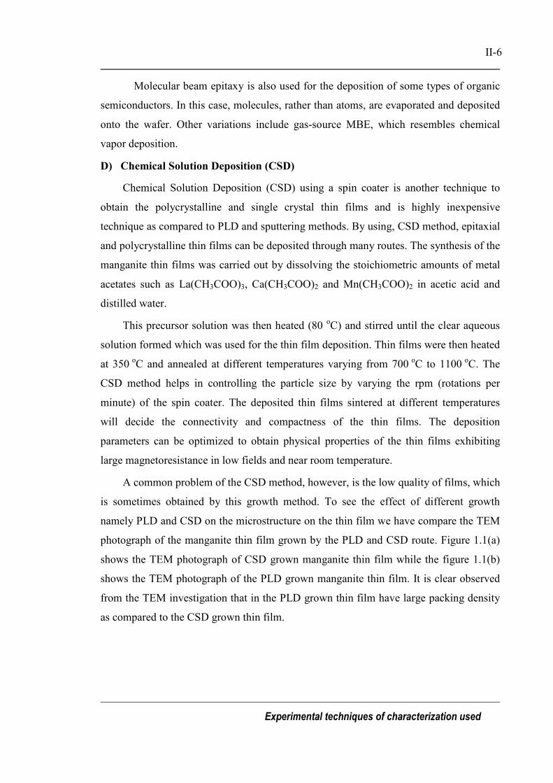
Experimental techniques of characterization used
II-6
Molecular beam epitaxy is also used for the deposition of some types of organic
semiconductors. In this case, molecules, rather than atoms, are evaporated and deposited
onto the wafer. Other variations include gas-source MBE, which resembles chemical
vapor deposition.
D) Chemical Solution Deposition (CSD)
Chemical Solution Deposition (CSD) using a spin coater is another technique to
obtain the polycrystalline and single crystal thin films and is highly inexpensive
technique as compared to PLD and sputtering methods. By using, CSD method, epitaxial
and polycrystalline thin films can be deposited through many routes. The synthesis of the
manganite thin films was carried out by dissolving the stoichiometric amounts of metal
acetates such as La(CH3COO)3, Ca(CH3COO)2 and Mn(CH3COO)2 in acetic acid and
distilled water.
This precursor solution was then heated (80 oC) and stirred until the clear aqueous
solution formed which was used for the thin film deposition. Thin films were then heated
at 350 oC and annealed at different temperatures varying from 700 oC to 1100 oC. The
CSD method helps in controlling the particle size by varying the rpm (rotations per
minute) of the spin coater. The deposited thin films sintered at different temperatures
will decide the connectivity and compactness of the thin films. The deposition
parameters can be optimized to obtain physical properties of the thin films exhibiting
large magnetoresistance in low fields and near room temperature.
A common problem of the CSD method, however, is the low quality of films, which
is sometimes obtained by this growth method. To see the effect of different growth
namely PLD and CSD on the microstructure on the thin film we have compare the TEM
photograph of the manganite thin film grown by the PLD and CSD route. Figure 1.1(a)
shows the TEM photograph of CSD grown manganite thin film while the figure 1.1(b)
shows the TEM photograph of the PLD grown manganite thin film. It is clear observed
from the TEM investigation that in the PLD grown thin film have large packing density
as compared to the CSD grown thin film.
Experimental techniques of characterization used
II-7
Figure:2.1: TEM photograph of (a) CSD deposited (b) PLD deposited manganite
thin film.
In particular, they have very low ferromagnetic Tc or TP (where the resistivity
peaks at the onset of ferromagnetic transition) and rather high resistivity. We note that
these problems are not generic to the chemical route. These problems can arise because
of a number of reasons, like the use of improper substrate, unoptimized growth condition
and uncontrolled grain morphology. These problems can even arise in more sophisticated
growth processes like PLD, MBE or MOCVD.
2.2 Structural Study
It is very essential to study structural properties of any material in order to
verify single phase structure before carrying any other studies on the material. Structural
properties are closely related to the chemical characteristics of the atoms in the material
and thus form the basics on which detailed physical understanding is built.
X-Ray Diffraction (XRD)
X-Rays are very small in wavelength that it can pass through most of the solid
materials. The wavelengths of x-rays are of the same order of magnitude as the distances
between atoms or ions in a molecule or crystal. While passing through a crystal, these
rays diffract by atoms at specific angles depending on the x-ray wavelength, the crystal
orientation, and the structure of the crystal. X-rays are predominantly diffracted by
electrons and analysis of the diffraction angles produces an electron density map of the
crystal. Crystalline materials can be described by their unit cell. This is the smallest unit
describing the material. In the material this unit cell is then repeated over and over in all
directions. This will result in planes of atoms at certain intervals. The diffraction method
is based on this fact of repetition and on Bragg’s law which gives a relation between the
distance from one atomic plane to the next, d, and the angle, θ, in which constructive

Experimental techniques of characterization used
II-8
interference of a reflected monochromatic beam is seen. The Bragg’s law follows the
equation given below.
2dsin(θθθθ) = nλλλλ [2.1][2.1][2.1][2.1]
where d = Inter planar distance, n = order of reflection (Integer value), λλλλ = Wave length
of X-rays, θ = Angle between incident/ reflected beam and particular crystal
planes under consideration.
We can see from equation 2.1 (Bragg’s law) that we need a beam with single,
well defined, frequency (monochromatic) in order not to have interference in more than
one direction for each planar distance. To obtain angles we can resolve with our
detectors also, need this wavelength to be of order “d”. Sintered samples contain grains
with planes distributed in all directions. Scanning in 2θ, the angle between the incident
beam and the diffracted beam, gives a diffraction pattern with peaks corresponding to the
different planar distances. Figure 2.2 represents the Bragg’s law.
At the first glance, the diffraction of x-rays by crystals and the reflection of
visible light by mirrors appear very similar, since in both phenomena the angle of
incident is equal to the angle of reflection. It seems that we might regard the planes of
atoms as little mirrors which reflect the x-rays. Diffraction and reflection however, differ
fundamentally in at least three aspects:
Figure: 2.2: Diffraction of X-rays by a crystal planes (Bragg’s law).

Experimental techniques of characterization used
II-9
1. The diffracted beam from a crystal is built up from rays scattered by all the atoms
of the crystal which lie in the path of the incident beam. The reflection of visible
light takes place in a thin surface layer only.
2. The diffraction of monochromatic x-rays takes place only at those particular
angles of incidence which satisfy the Bragg’s law. The reflection of visible light
takes place at any angle of incidence.
3. The reflection of visible light by a good mirror is almost 100 percent efficient.
The intensity of a diffracted X-ray beam is extremely small compared to that of
the incident beam.
According to figure 2.2, two noteworthy things are: a) The incident beam,
normal to the reflecting plane, and the diffracted beam are always coplanar. b) The angle
between the diffracted beam and the transmitted beam is always 2θ, which is usually
measured experimentally. The detailed description of XRD is given in references.
Set up for X-ray diffractometer consists of an x-ray generator, a goniometer and a
sample holder. One x-ray detector is required as a photographic film or a movable
proportional counter. X-rays are generated in x-ray tube by bombarding a metal target
with high-energy (10 - 100 keV) electrons. Two targets commonly used are of Mo and
Cu, which have strong K (alpha) x-ray emission at 0.71073 Å and 1.5418 Å,
respectively. X-rays can also be generated by decelerating electrons in a target or a
synchrotron ring. These sources produce a continuous spectrum of x-rays and require a
crystal monochromator to select a single wavelength. Finally, the diffracted x-rays are
detected in x-ray detector. The sample is scanned over a range of 2θ.
Applications of XRD
XRD is nondestructive technique
To identify crystalline phase and orientation
To determine structural properties: Lattice parameters, strain, grain size, expitaxy,
phase composition, preferred orientation, (Laue) order-disorder transformation,
thermal expansion
To measure thickness of thin films and multi-layers

Experimental techniques of characterization used
II-10
To determine atomic arrangement
2.3 Surface Morphology
Morphological studies are important for understanding the growth and packing
density of grains in thin films or polycrystalline bulk materials. There are various
techniques known to explore the science related to structure and morphology of a
material. These are used to ascertain single phase samples and detect deviations from the
main structure as well as extracting the actual structure. The different techniques have
different advantages and disadvantages and thus complement each other.
To study morphology of the samples, generally, AFM or SEM are widely used
experimental techniques. TEM is useful tool to see cross sectional view of the thin films,
especially when thin films are irradiated or exhibit defects in the inner structure. TGA
and Iodometric titration are generally used to study oxygen stoichiometry of the
materials. Most of the experimental techniques are used to characterize the samples
under present studies.
Scanning Electron Microscopy (SEM)
SEM stands for scanning electron microscope. The SEM is a microscope which
uses electrons as probes to form an image of a specimen. The major development of
SEM took place on 1950’s but then it advanced to various fields of research such as
surface studies in material science for about two decades. M Knoll produced the first
scanned image of a surface in 1935, but later Von Ardenne laid the foundations of both
transmission and surface scanning electron microscopy. Later, it was Charles Oatley, in
Cambridge in 1947 who spent the better part of two decades before reaching a successful
conclusion with the world-wide acceptance of the SEM as one of the most powerful and
productive methods of microscopy yet invented .
The SEM has allowed researchers to examine a large variety of specimens. The
scanning electron microscope has many advantages over traditional microscopes. The
SEM has a large depth of field, which allows more of a specimen to be in focus at one
time. The SEM also has much higher resolution; so closely spaced specimens can be
magnified at much higher levels. As the SEM uses electromagnets rather than lenses, it

Experimental techniques of characterization used
II-11
is much more controlled in the degree of magnification. All of these advantages, as well
as the actual strikingly clear images, make the scanning electron microscope one of the
most useful instruments in research today.
Scanning Electron Microscope (SEM) has become a valuable tool for
examination and evaluation of materials, both metallic and non-metallic, as well as
assemblies and surfaces. This is a non-destructive technique in a way that, sample can be
extracted after scanning. The sample to be investigated is placed on a specimen stage
inside a vacuum enclosure of the SEM station and is incident with a finely focused
electron beam that can be static or swept in a cyclic fashion over the specimen's surface.
The resulting signals that are produced when the scanning electron beam impinges on the
surface of the sample include both secondary emission electrons as well as backscattered
electrons. These signals vary as the result of differences in the surface topography as the
scanning electron beam is swept across the sample surface.
(a) Basic set up of SEM
The basic parts of a typical Scanning Electron Microscope include
1. Vacuum Enclosure with sample mounting stage to hold the sample.
2. Electron gun to produce the scanning electron beam.
3. Secondary electron detector and collector circuits for Emitted Secondary
electrons.
4. Electronic Elements such as Signal Amplifier and Signal Conditions, etc.
5. Cathode Ray Tube (CRT), Display Unit and magnetic lens Elements etc.
6. Positioning Controls including Tilt for movement and offset of the test object.
7. Additions such as Camera, Video Recorder and additional CRT's.

Experimental techniques of characterization used
II-12
(b) Working of SEM
The SEM produces a largely magnified image by using electrons instead of light
to form an image. A beam of electrons is produced at the top of the microscope by an
electron gun. The electron beam follows a vertical path through the microscope, which
is held within a vacuum. The beam travels through electromagnetic fields and lenses,
which focus the beam down toward the sample. Once the beam hits the sample,
electrons and X-rays are ejected from the sample.
Figure 2.3: A diagram showing the working of scanning electron microscope
(SEM) (Diagram courtesy of Iowa State University SEM Homepage).

Experimental techniques of characterization used
II-13
Detectors collect these X-rays, backscattered electrons, and secondary electrons
and convert them into a signal that is sent to a screen similar to a television screen. This
produces the final image. The secondary emission of electrons (fig. 2.4) from the
specimen surface is usually confined to an area near the beam impact zone that permits
images to be obtained at a relatively high resolution. These images as seen on a Cathode
Ray Tube provide a three dimensional appearance due to the large depth of field of the
Scanning Electron Microscope (SEM) and the shadow relief effect of the secondary
electrons contrast. Figure 2.3 represents the schematic diagram of SEM explaining the
experimental set up.
Figure: 2.4: The outcomes of incident electron beam in a SEM.
A typical SEM has a working magnification range from 10 to 100,000 diameters.
A resolution can be attainable of 100 Å, and a focus of 300 times that of an optical
microscope. The large depth of field available with a SEM makes it possible to observe
three-dimensional objects. The three-dimensional images produced, allow different
morphological features to be correctly interrelated and correctly analyzed.
(c) Benefits of SEM
The unique advantage of Scanning Electron Microscopy is that, it does not need
much samples loading activity and also, the thickness of the specimen is not a
consideration. The surface of the sample may cleaned and smoothened before it is
scanned. This helps in achieving better surface morphological and grain size information.

Experimental techniques of characterization used
II-14
Atomic Forced Microscopy (AFM)
In Atomic Forced Microscopy (AFM), a sharp probe is scanned on a flexible
lever (cantilever) relative to a material of interest. AFM (fig. 2.5) operates by measuring
attractive or repulsive forces between a tip and the sample. The cantilever responds to
valleys and other features of the sample surface that it encounters while scanning the
material surface. These reactions are recorded and produce an image of the material’s
surface showing the presence of humps and valleys on the surface, resembling a surface
topographic map. The basic objective of the operation of the AFM is to measure the
forces (at the atomic level) between a sharp probing tip (which is attached to a cantilever
spring) and a sample surface. Images are taken by scanning the sample relative to the
probing tip and measuring the deflection of the cantilever as a function of lateral
position. Now most AFM employ an optical lever technique. The diagram illustrates how
this works; as the cantilever flexes, the light from the laser is reflected onto the split
photo-diode. By measuring the difference signal (A-B), changes in the bending of the
cantilever can be measured (fig. 2.5).
Figure 2.5: Working of optical cantilever in AFM
(a) Contact mode AFM
One method of AFM is the use of contact mode. In this method the cantilever
remains in contact with the surface during scanning. When it encounters variations on
Experimental techniques of characterization used
II-15
the surface, it responds by deflecting to follow the contours. This process produces
accurate topographical maps of the surface for different type of samples, but there are
some unwanted drawbacks in this method. Due to continuous contact of the cantilever on
the surface of the sample, damage to the surface can occur which can then alter both the
resulting image and properties of the material. To counter this problem, a new method
called ‘tapping mode’ was developed. In this mode, the cantilever arm is oscillating at a
resonant frequency, as it scans the surface. When the tip begins to slightly touch the
surface, a sensor reverses the motion of the cantilever to continue the oscillation. The tip
then intermittently touches the surface, instead of being dragged and introducing damage
as in contact mode. But since the cantilever is not in continuous contact with the surface,
a method of measuring the differences in the surface height must be determined. This
results from changes in the amplitude of oscillation of the cantilever. When it encounters
bumps on the surface, the amplitude of oscillation is reduced. Conversely, valleys or
depressions cause the amplitude to increase. By recording these changes, an accurate
topographical map can be produced without damaging the surface of the material.
Thin film samples in the present work are characterized by contact mode AFM
working on the principle of optical cantilever.
(b) Noncontact mode AFM
In noncontact mode, the AFM derives topographic images from measurements of
attractive forces; the tip does not touch the sample. A rich variety of forces can be sensed
by atomic force microscopy. In non-contact mode (With distances greater than 10Å
between the tip and the sample surface), Vander Waals, electrostatic, magnetic or
capillary forces produce images of topography, whereas in the contact mode, ionic
repulsion forces take the leading role. Because its operation does not require a current
between the sample surface and the tip, the AFM can move into potential regions
inaccessible to the Scanning Tunnelling Microscope (STM) or image fragile samples
which would be damaged irreparably by the STM tunnelling current. Insulators, organic
materials, biological macromolecules, polymers, ceramics and glasses are some of the
many materials which can be imaged in different environments, such as liquids, vacuum,
and low temperatures.

Experimental techniques of characterization used
II-16
The basic objective of the operation of the AFM in any mode is to measure the
forces (at the atomic level) between a sharp probing tip (which is attached to a cantilever
spring) and a sample surface. Images are taken by scanning the sample relative to the
probing tip and measuring the deflection of the cantilever as a function of lateral
position.
2.4 Electronic Transport and Magnetoresistive Properties
The bulk samples, targets, thin films and hetrostructure studied during the preset
work were characterized for their electrical and magneto transport properties by using
the experimental techniques described below.
2.4.1 D.C. four-probe method
Transport property measurements of the manganite thin films were carried out using
standard four –terminal method on a Quantum Design PPMS system and home made
receptivity set-up with the liquid Nitrogen Dewar. The PPMS system can conduct the
measurements in the temperature range of 1.9 - 350K. Temperature sweep capability
allows measurements to be taken while sweeping the temperature at a user defined rate
(0.01-6 K/min). Continuous low temperature control (CLTC) ensures precise
temperature control. The PPMS has a superconductor magnet, which can provide a
magnetic field up to 9 Tesla with the uniformity of 0.01% over a 5.5 cm×1cm diameter
cylindrical volume. The low noise, bi-polar power supply allows continuous charging
through zero field with current compensation and over-voltage protection. The resolution
of the field control is 0.02 mTesla up to 9 Tesla. A schematic illustration of the PPMS
probe is shown in Figure 2.6. Samples were mounted on removable platforms (see
picture 2.1). A thermometer, in direct contact with the platform, accurately determines
the sample temperature. The rotator can sweep the angular range from-10 oC to 370 oC ,
with the step size of 0.053° for standard resolution. A low contact resistance is desirable
due to the small resistance of the samples. To fulfill this requirement, standard four-
probe method was used for measuring resistance of the samples. To measure the
resistivity using this technique, the samples were cut in a rectangular bar shape using a
diamond saw. For making electrical contacts of the probes with the sample silver paint
was used. Fine slurry of the silver paint was made by dissolving it with an appropriate
solvent (n-butyl acetate or thinner). This silver paste was applied at the ends for current

Experimental techniques of characterization used
II-17
and voltage contacts. Due to very less resistance, thin copper wires were connected with
silver paint as shown in fig.2.6 and the whole assembly was attached to a sample holder,
where the wires were connected with leads to the measurement instruments. Such a
sample holder is known as resistivity puck for measuring resistivity using a Physical
Property Measurement System (PPMS). A schematic illustration of PPMS is shown in
the picture 2.2 and photograph of home made RT & Magneto-RT measurements set up
shown in the picture 2.3
Figure 2.6: Four probe contacts used in the resistivity measurements.
Picture: 2.1: Sample rotator with sample mounting platform.

Experimental techniques of characterization used
II-18
Picture:2.2: A schematic illustration of the PPMS
Picture:2.3: Photograph of R-T and Magneto-RT (1T) setup.

Experimental techniques of characterization used
II-19
2.4.2 MR measurements (Low field and High field)
To study magneto resistive characteristics of the samples, resistance was measured
by using the standard four probe method as explained in the previous section, in the
presence of an external magnetic field in a Quantum Design Physical Property
Measurement System (PPMS). At a constant applied field, resistance was measured as a
function of temperature (magneto R-T) in the range of RT-5 K. All the manganite
samples studied in the present work were characterized by using this technique.
2.5 Magnetic susceptibility and magnetization measurements
2.5.1 D.C. magnetization
Superconducting Quantum Interference Device (SQUID) magnetometer is the most
powerful, sensitive and widely used instrument for magnetic characterization in material
science. This device works on the principal of quantum interference produced using
Josephson junctions. This Josephson junction (sensor) mainly consists of the
superconducting ring interpreted by a thin insulting film called weak link. The sensor
and its pick up system is sensitive to change in the magnetic fluxes and thus to the
change of the magnetization of magnetic material as a function of temperature, magnetic
field and time. The SQUID has one or more Josephson junctions as its active element.
In most practical systems in use today, the SQUID is located inside a small
cylindrical, superconducting magnetic shield in the middle of a liquid helium Dewar.
Superconducting pickup coils, typically configured as gradiometers that detects the
difference in one component of the field between two points, are located at the bottom of
the Dewar, and are placed beneath the magnetometer. The rest of the hardware is
designed to minimize helium boil off, eliminate rf interference, and avoid Johnson noise
or any external distortion a. c. fields. If a constant biasing current is maintained in the
SQUID device, the measured voltage oscillates according to the changes in phase at the
two junctions, which depends upon the change in the magnetic flux. The flux change can
be evaluated by counting the oscillations. It may be noted that the sensitivity of SQUID
is 10-14 Tesla, which is incredibly large to measure any magnetic signal.
Experimental techniques of characterization used
II-20
Vibrating Sample Magnetometer
Vibrating sample magnetometer (VSM) is used to measure the magnetic moment
of a material. A VSM operates on Faraday's Law of Induction. According to Faraday’s
laws of magnetic induction, an ac voltage is induced which is proportional to the rate of
change of magnetic flux associated with the circuit and thus to the amount of magnetic
moment within the sample due to the applied magnetic field. A VSM operates by first
placing the sample to be studied in a constant magnetic field. If the sample is magnetic,
this constant magnetic field will magnetize the sample by aligning the magnetic domains
or the individual magnetic spins, with the field. If the constant field is larger, the
magnetization will also be larger. The magnetic dipole moment of the sample will create
a magnetic field around the sample, sometimes called the magnetic stray field. The
sample is vibrated with a certain frequency in the vertical direction near the detection
coil. As the sample is moved up and down, this magnetic stray field changes as a
function of time and can be sensed by a set of pick-up coils. An ac signal is generated at
a frequency determined by the sample oscillation. This electric field can be measured
and can give us information about the changing magnetic field. This current will be
proportional to the magnetization of the sample. The greater the magnetization, the
greater will be induced current.
Oxford instruments design VSM is used for these measurements with a few Tesla
superconducting magnet. The material under investigation is mounted in a sample holder
at the end of a carbon fiber rod and inserted in VSM continuous flow Helium Cryostat.
The tail of the cryostat lies inside a conventional NbSn superconducting magnet capable
of sustained fields up to 12 Tesla.
Once a DC field is applied, the sample is vibrated at a constant frequency of
66 Hz with amplitude of about 1.5mm along the vertical axis of the uniform applied
field. Two pickup coils, placed above and below the sample, experience a change of the
magnetic flux due to the motion of the sample and, according to Faraday's law, an emf
induced is proportional to the rate of that change of flux. This signal, proportional to the
magnetization of the sample, passes through a two-stage amplification process and is
monitored by the VSM electronics and recorded on a computer via a standard RS232

Experimental techniques of characterization used
II-21
connection. The sample temperature is measured by a AuFe/Chromel thermocouple in
direct contact with a copper heat exchanger situated below the sample.
Figure: 2.7: A Schematic diagram of VSM.
The temperature control (temperature range: 3.6 - 320 K) is achieved by an Oxford
Instruments ITC4 temperature controller. A schematic diagram is shown in fig. 2.7.
The above-mentioned measurement systems are used for d. c. magnetization and M
versus H measurements of the samples. For d. c. magnetization a small external field is
applied and χ is measured as a function of temperature at constant applied field. For M-H
measurements, magnetization is measured at a constant temperature while magnetic field
is varied up to a certain value of positive and negative applied field. The most common
units for the magnetic moment is emu. The natural unit of the magnetization is thus
emu/g or emu/cm3. If one can estimate the number of atom in the sample then one can
also calculated the magnetic moment per atom in µB.
2.5.2 A.C susceptibility
In ac susceptibility ( χχχχac) measurements the magnetization is probed by a small
sinusoidal field of frequency f. The susceptibility measurement provides the information
about the curie temperature (TC), magnetic ordering in the materials.

Experimental techniques of characterization used
II-22
0 100 200 3000
4
8
12
ZFC
FC H=50 Oe
M (emu/gm)
T (K)
Figure:2.8: Temperature dependence of the FC and ZFC magnetization.
If a magnetic material get magnetized in the direction of the magnetic flux lines and
shows a certain finite magnetic susceptibility ( χχχχ ), which is defined as ratio of
magnetization (M) to the applied magnetic field (H). The dynamic susceptibility has two
components: one component is in-phase ( χχχχ ′′′′ ) with the excitation while other one is a
dissipative out of phase ( χχχχ ′′′′′′′′ ) component. Susceptibility can be measured on cooling or
heating the sample.

Experimental techniques of characterization used
II-23
REFERENCES
1. E. M. Engler
Chem. Technol. 17 542 (1987).
2. S. X. Dou, H.K. Liu, A.J. Bourdillon, J. P. Zhou, N.X. Tan, X.Y. Sun,
C.C. Sorrell and J. Am.
Ceram. Soc. 71C 329 (1998).
3. C. J. Brinkered and G. W. Scherer
“Sol-Gel Science” Academic Press Inc, Boston (1990).
4. D. B.Chrisery and G. K.Hubler
“ Pulsed Laser Deposition” Wiley-Interscience, New York, (1994).
5. Young Sun, M. B. Salamon and S. H. Chun
J. Appl. Phys. 92 3235 (2002).
6. B. D. Cullity, “X-ray Diffraction” Addison-Wesley, New York (1972).
7. C. Kittel ,“Introduction to Solid State Physics” New York, Plenum (1966).
8. A. Taylor, “X-ray Metallography” John Wiley & Sons (1961).
9. H. M. Rietveld, J. Appl. Cryst. 2 65 (1969).
10. R. A. Young
“The Rietveld Method” Oxford University Press Inc, New York (1993).
11. G. Binnig, C. F. Quate and Ch. Gerber
Phys. Rev. Lett. 56(9) 930 (1986).
12. G. Meyer and N. M. Amer, Appl. Phys. Lett. 57(20) 2089 (1990).
13. PPMS manual by Quantum Design.
14. L. J. Vanderpauw
Philips Res. Repts. 16 187 (1961).
15. SQUID Magnetometer, Manual by Quantum Design.

Chapter - 3

Irradiation studies on manganite thin film
III - 1
3.1 Introduction
The manganites of the type RE1-xMxMnO3, where RE and M are trivalent rare
earth and diavalent alkaline earth element respectively, exhibit several interesting
properties due to the interplay of magnetism, electric transport, and crystallographic
distortion. Much interest has been focused on the hole doped ferromagnetic phase (x ≈ 0.3)
that exhibits colossal magnetoresistance[1]. At fractional doping level, another mechanism
is superimposed: charge ordering between Mn+3 and Mn+4 ions [2-5]. The crystallographic
and magnetic environment is then strongly modified. For instance, Nd0.5Sr0.5MnO3 is
ferromagnetic and metallic below 245K [3, 5]. At 160 K, the charge order transition occurs
and the system becomes antiferromagnetic and insulating. Applying a strong magnetic
field restores the ferromagnetic order together with the metallic conductivity.
However, these properties depend crucially on the local lattice distortion and the
mismatch between the rare earth and the alkaline element [6,7]. In these perovskite
structures, it is convenient to define the tolerance factor t = (rLE,M+rO)/√2(rMn+rO) where
rLE,M, rMn, and rO are the average ionic radii of the trivalent rare earth and divalent alkaline
earth site, manganese site and oxygen site, respectively. It describes the distortion of the
perovskite structure. This distortion modifies the strength of the different magnetic
interactions present in these systems. The double exchange mechanism couples the
itinerant 3deg electrons of Mn3+ with the localized 3dt2g spins of the Mn4+ ions. It depends
on the number of eg electrons as well as the bond angle Mn-O-Mn governed by the lattice
distortion. On the other hand, the superexchange interaction between manganese ions
favors antiferromagnetic order with localized spins with then insulating electric properties.
Decreasing the ionic radius of the L and M site modifies the bond angle Mn-O-Mn and
than the ferromagnetic ordering interaction is reduced[6]. The bandwidth of eg electron
becomes narrower. Eventually, the system becomes insulating and loses its ferromagnetic
order. To this way, size disorder significantly effect the electrical transport and magneto
transport system.
Variations in the characteristics of the manganite thin films due to the swift heavy
ions (SHI) irradiation is an exciting but not yet fully understood area of research [8, 9]. It
is an established fact that SHI irradiation is responsible for the dramatic changes in the

Irradiation studies on manganite thin film
III - 2
transport and magnetic properties of manganite because it creates the effects like changes
in the surface morphology, magnetic anisotropy, columnar or point defect formation,
amorphization of the material, etc. [8-10]. It has also been reported that the resistivity of
the films increases after irradiation by SHI [11]. We have, on the contrary, observed that
the resistivity of the La0.7Ca0.3MnO3 (LCMO) thin films is suppressed due to 200 MeV
Ag15+ ion irradiation. This anomalous observation and its possible reasons are presented
and discussed in this chapter.
3.1.1 Synthesis
Polycrystalline bulk target sample of La0.7Ca0.3MnO3 was synthesized by using
standard ceramic method. Dried powders of La2O3, CaCO3 and MnO2 (all > 99.9% pure)
were mixed in stoichiometric proportions and calcined at 950°C for 24 hours. The mixture
was then ground, pelletized and sintered in the temperature range of 1100°C-1400°C with
several intermediate grindings. The final well-sintered 15mm diameter pellet was used as a
target for the deposition of single crystalline epitaxial thin films of La0.7Ca0.3MnO3 using
Pulsed Laser Deposition (PLD) technique. Third harmonic (355 nm) of a Q-switched Nd:
YAG laser (6ns) having energy density of about 2.17 J/cm2 at 10 Hz repetition rate was
used for the ablation. Polished (h00) LaAlO3 (LAO) single crystal substrates were placed
in front of the target at a distance of 5.5 cm and heated to 740°C. The chamber was first
pumped down to 10-5 bar. The laser deposition process was carried out at in an oxygen
partial pressure of 400 mTorr.
The deposited films were having a thickness of 100nm. Swift Heavy Ion (SHI)
irradiation was carried out using 200 MeV Ag15+ ions at a fluence of about 5 × 10¹¹
ions/cm2 at the 15-UD Tandem Accelerator. The irradiation was performed at a low angle
with respect to the ion beam to avoid the channeling effect. The ion beam was focused to a
spot of about 1 mm diameter on the sample and was scanned over a 10 × 10 mm area using
a magnetic scanner in order to irradiate the thin film over a sufficiently large area with
uniformity.
The structure of the samples was analyzed using X-ray diffraction (XRD) and
surface morphology was studied using Atomic Force Microscopy (AFM). The resistivity

Irradiation studies on manganite thin film
III - 3
was measured as a function of temperature in range of 5 K – 320 K and as a function of
magnetic film recorded as 0T-9T using PPMS facility at TIFR, Mumbai.
3.2 Structural Study and Surface Morphology
3.2.1 Structural study
The rietveld fitting of the XRD data of La0.7Ca0.3MnO3 bulk target showed that the
sample crystallizes in orthorhombic Pnma type of structure with cell parameters
a = 0.5123(2) nm, b = 0.7681(2) nm, c = 0.5132(2) nm. The XRD patterns of pristine and
irradiated La0.7Ca0.3MnO3/LAO thin films were indexed using orthorhombic cell
parameters of bulk compound. Figure 3.1 and 3.2 shows, the indexed XRD peaks of
100nm pristine and irradiated La0.7Ca0.3MnO3/LAO thin film, respectively. From the XRD
patterns, it can be seen that, both the films possess epitaxial growth in (h0l) direction.
Figure 3.3 shows comparison of XRD patterns of La0.7Ca0.3MnO3/LAO pristine and
irradiated thin films, while figure 3.4 denotes the enlarged view of (202) peak of the
pristine and irradiated La0.7Ca0.3MnO3/LAO thin films. It can be seen from the figure 3.4
that, in 100 nm pristine film, (202) peak located at ∼ 46.38° shifts to lower angle ∼ 45.72°
after irradiation. This observation has an effect on the strain present in the film. The lattice
mismatch δ along the interface has been calculated using the following formula.
100×−
=substrate
filmsubstrate
d
ddδ
The negative value of mismatch corresponds to the compressive strain [11]. In the
pristine La0.7Ca0.3MnO3/LAO thin film compressive strain is ∼ -0.89 and in the irradiated
thin film it is ∼ -0.25. This suggest that after irradiation strain is released the film lattice.

Irradiation studies on manganite thin film
III - 4
20 30 40 50 60
0
5
10
15
20
25
30
LAO LAO
(200)
(202)
(100)
(101)
La0.7
Ca0.3
MnO3/LAO
Pristine
Inte
nsit
y (a
.u.)
2θ (degree)
Figure 3.1: A typical XRD pattern of 100 nm La0.7Ca0.3MnO3/LAO films (Pristine).
20 30 40 50 60
0
5
10
15
20
25
30
LAO
LAO
La0.7
Ca0.3
MnO3/LAO
Irradiated
(200)
(202)
(100)
(101)
Inte
nsit
y (a
.u.)
2θ (degree)
Figure 3.2: A typical XRD pattern of 100 nm La0.7Ca0.3MnO3/LAO films (Irradiated).

Irradiation studies on manganite thin film
III - 5
20 30 40 50 600
5La
0.7Ca
0.3MnO
3/LAO
(200)(100)
(101)(202)
Inte
nsit
y (a
.u.)
2θ (degree)
Pristine Irradiated
Figure 3.3: A typical XRD pattern of 100 nm La0.7Ca0.3MnO3/LAO films (Pristine and
Irradiated).
44 45 46 47 48 49 500
500
1000
1500
2000
2500
3000
(200)
(202)
La0.7
Ca0.3
MnO3/LAO
Inte
nsit
y (a
.u.)
2θ (degree)
Pristine Irradiated
Figure 3.4: Enlarged view of indexed patterns of 100 nm La0.7Ca0.3MnO3/LAO
films (Pristine and Irradiated).
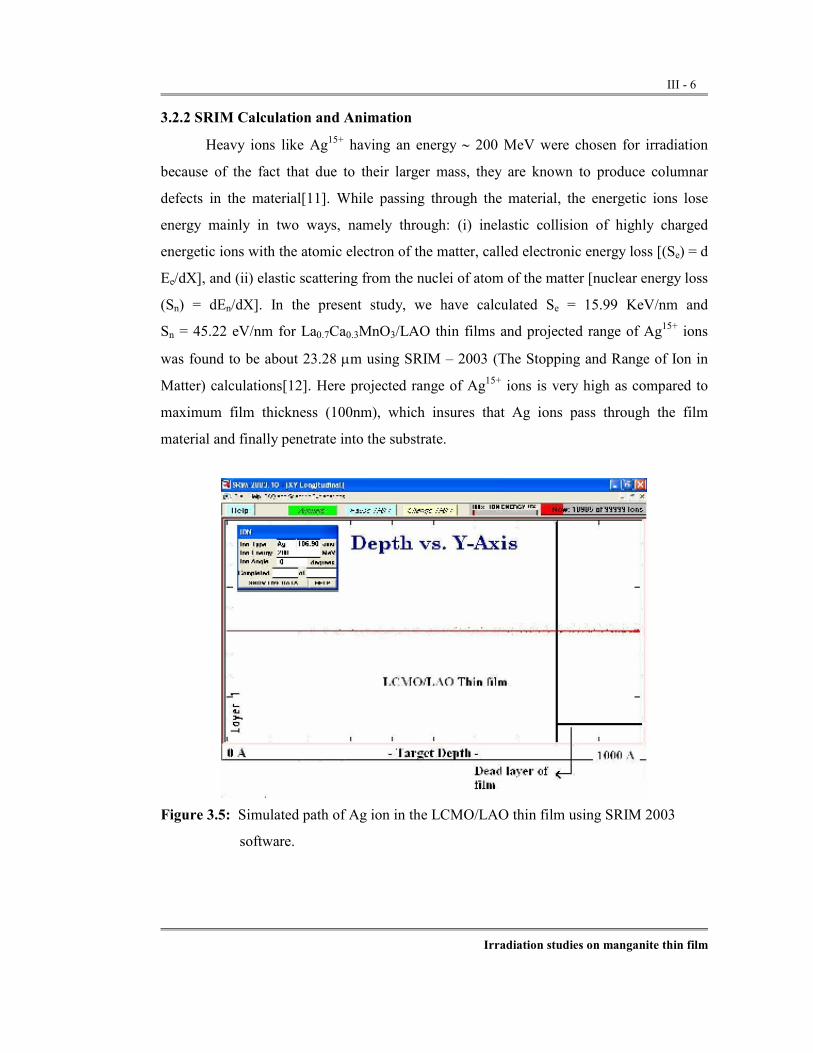
Irradiation studies on manganite thin film
III - 6
3.2.2 SRIM Calculation and Animation
Heavy ions like Ag15+ having an energy ∼ 200 MeV were chosen for irradiation
because of the fact that due to their larger mass, they are known to produce columnar
defects in the material[11]. While passing through the material, the energetic ions lose
energy mainly in two ways, namely through: (i) inelastic collision of highly charged
energetic ions with the atomic electron of the matter, called electronic energy loss [(Se) = d
Ee/dX], and (ii) elastic scattering from the nuclei of atom of the matter [nuclear energy loss
(Sn) = dEn/dX]. In the present study, we have calculated Se = 15.99 KeV/nm and
Sn = 45.22 eV/nm for La0.7Ca0.3MnO3/LAO thin films and projected range of Ag15+ ions
was found to be about 23.28 µm using SRIM – 2003 (The Stopping and Range of Ion in
Matter) calculations[12]. Here projected range of Ag15+ ions is very high as compared to
maximum film thickness (100nm), which insures that Ag ions pass through the film
material and finally penetrate into the substrate.
Figure 3.5: Simulated path of Ag ion in the LCMO/LAO thin film using SRIM 2003
software.

Irradiation studies on manganite thin film
III - 7
Figure 3.5 shows a simulation of 200 MeV Ag+15 passes through the
La0.7Ca0.3MnO3/LAO thin film (using the SRIM-2003 software). This figure shows the ion
throughout passes the film material and produce columnar like defect.
3.2.3 Surface Morphology
Figure 3.6 depicts the AFM photograph of pristine La0.7Ca0.3MnO3/LAO thin film
(2D image) while figure 3.7 shows the 3D image of the same thin film. Figs. 3.8 & 3.9
shows the 2D & 3D image respectively, of the irradiated La0.7Ca0.3MnO3/LAO thin film
with 200 MeV Ag+15 ion with fluence of 5 × 10¹¹ ions/cm2. Surface modification after ion
bombardment clearly seen from the figs. 3.8 & 3.9. From this, it can be said that, track like
defects are formed which possess an average diameter of ∼ 100nm. From the calculation
of size of the track like defects, it can be concluded that this size is quite large as compared
to normal columnar defect size. Also the out growths present next to columnar like defects
could be arising due to the energetic ions striking the surface-producing spike like
structures.
200nm
Figure 3.6: shows the 2D image of pristine La0.7Ca0.3MnO3/LAO thin film

Irradiation studies on manganite thin film
III - 8
Figure 3.7: shows the 3D image of pristine La0.7Ca0.3MnO3/LAO thin film
430nm
Figure 3.8: shows the 2D image of the irradiated La0.7Ca0.3MnO3/LAO thin film

Irradiation studies on manganite thin film
III - 9
Figure 3.9: shows the 3D image of the irradiated La0.7Ca0.3MnO3/LAO thin film
3.3 Electronic transport properties
The temperature dependence of the resistance curves for the 1000Å pristine
La0.7Ca0.3MnO3/LAO thin film shown in figure 3.10, having TIM value ∼ 212 K. The figure
3.11 shows the resistance vs. temperature plot for the irradiated La0.7Ca0.3MnO3/LAO thin
film with the 200 MeV Ag+15 ion with the fluence of 5 × 10¹¹ ion/cm2. Irradiated
La0.7Ca0.3MnO3/LAO thin film shows the TIM value ∼ 232 K.

Irradiation studies on manganite thin film
III - 10
0 50 100 150 200 250 300 350
0
5
10
15
20
25
30
35
H = 0T H = 5T H = 9T
La0.7
Ca0.3
MnO3/LAO
Pristine
Res
ista
nce
(KΩ
)
Temperature
Figure 3.10: Resistance vs. Temperature plots of 100 nm La0.7Ca0.3MnO3/LAO
films (Pristine).
0 50 100 150 200 250 300 350
0.0
0.5
1.0
1.5
2.0 La0.7
Ca0.3
MnO3/LAO
Irradiated
(5X10¹¹
ions/cm2)
Res
ista
nce
(KΩ
)
Temperature
H = 0T H = 5T H = 9T
Figure 3.11: Resistance vs. Temperature plots of 100 nm La0.7Ca0.3MnO3/LAO
films (Irradiated).

Irradiation studies on manganite thin film
III - 11
0 50 100 150 200 250 300 350
0.0
0.5
1.0
1.5
2.0
2.5
3.0
0T
La0.7
Ca0.3
MnO3/LAO
Res
isti
vity
(Ω
cm
)
T (K)
Pristine Irradiated
Figure 3.12: Resistivity vs. Temperature plots of 100 nm La0.7Ca0.3MnO3/LAO
films (Pristine and Irradiated).
To identify the irradiation effect clearly, we have plot resistivity of both pristine
and irradiated thin film in the figure 3.12 and it can be clearly seen that resistivity is
suppressed by very larger factor (∼ 92%). Suppression in the resistivity as an effect of
irradiation is anormous behaviour because due to irradiation, defects are created which
increase the possibility of the scattering resulting in to higher resistance. Also TIM values
of irradiated film is increases as compared to the pristine thin film showing the increase
transport mechanism of spin in the Mn-O-Mn channel resulting in to higher magnetic
transition temperature. Also, the calculated projected range of Ag+15 ions in the
La0.7Ca0.3MnO3/LAO films is very larger than the thickness of the La0.7Ca0.3MnO3/LAO
film, means Ag ions passes through the La0.7Ca0.3MnO3/LAO film material and strike the
substrate. So this way, possibility of contribution of metallic Ag ion in the electronic
transport ( resistivity) is ruled out.
Now to understand the effect of irradiation on the transport property, we have done the
theoretical model fitting in the metallic and insulating region.

Irradiation studies on manganite thin film
III - 12
The resistivity data in the metallic region was fitted in the magnon scattering law
ρ(T) = ρ0 + BTn…………(1),
ρ0 is electron-magnon scattering coefficient [More detail is given in chapter 4, page
no.10].
Table 3.1: Denote the fitting parameter such as σ0, B, n, χ2 , and R
Sample
La0.7Ca0.3MnO3/
LAO
H σ0
(Ω1-cm-1)
B
(Ω cmK-1)
n χ2
R2
0T 0.01214 5.3E-13 5.175 5.521E-6 0.99065
Pristine 5T 0.01132 2.5E-9 3.315 2.098E-7 0.99843
0T 0.00302 3.3E-11 3.937 3.765E-8 0.99656 Irradiated
5T 0.00111 6.5E-10 3.073 5.871E-10 0.99925
0 20 40 60 80 100 120 140 1600.00
0.05
0.10
0.15
0T
La0.7
Ca0.3
MnO3/LAO
Pristine
ρ(Ω
cm)
T (K)
Figure 3.13: Resistivity vs.Temperature plots of 100 nm La0.7Ca0.3MnO3/LAO (Pristine).
The symbols are the experimental data points and the solid lines are the
theoretical fits.

Irradiation studies on manganite thin film
III - 13
0 20 40 60 80 100 120 140 1600.00
0.02
0.04
0.06
0.08
La0.7
Ca0.3
MnO3/LAO
Pristine 5T
ρ(Ω
cm)
T (K)
Figure 3.14: Resistivity vs. Temperature plots of 100 nm La0.7Ca0.3MnO3/LAO (Pristine).
The symbols are the experimental data points and the solid lines are the
theoretical fits.
0 20 40 60 80 100 120 140 1600.00
0.01
0.02
0T
La0.7
Ca0.3
MnO3/LAO
Irradiated
T (K)
ρ(Ω
cm)
Figure 3.15: Resistivity vs.Temperature plots of 100 nm La0.7Ca0.3MnO3/LAO(Irradiated).
The symbols are the experimental data points and the solid lines are the
theoretical fits.

Irradiation studies on manganite thin film
III - 14
0 20 40 60 80 100 120 140 1600.000
0.002
0.004
0.006La
0.7Ca
0.3MnO
3/LAO
Irradiated
T (K)
ρ(Ω
cm)
5T
Figure 3.16: Resistivity vs Temperature plots of 100 nm La0.7Ca0.3MnO3/LAO
(Irradiated). The symbols are the experimental data points and the solid lines
are the theoretical fits.
Figs. 3.13 to 3.16 shows the low temperature resistivity fitting to equation (1) with field
and without field and table 3.1 shows the obtained fitting parameters such as σ0, B, n, χ2 and
R. From the table and fitting plots, it can be clearly seen that, quality of fitting is very good
because χ2 is very less than 1 and R is near to 1. From the theoretical modeling, we can say
that σ0 (residual resistivity) is ∼ 0.01214 Ω-1cm-1 for the pristine La0.7Ca0.3MnO3/LAO
film which decreases up to 0.00302 Ω-1cm-1, means sharp decrease in the residual resistivity
as an effect of irradiation. That denotes the modification in the film super lattice by an effect
of irradiation. Also it is notable that, n value changes from 5 (pristine) to 4 (irradiated)
suggesting that, scattering mechanism do not change in both pristine and irradiated thin film.
Two magnon scattering is responsible for the transport mechanism in the metallic region.
In order to understand the conduction mechanism of polarons created as a result of
electron-phonon coupling in the semiconducting region and to understand the irradiation
effect on that, we fitted the ρ - T data of La0.7Ca0.3MnO3/LAO thin films (pristine and
irradiated). Mott’s type variable Range hopping model (VRH)[13] corresponding
ρ = ρο exp(Tο/T)1/4 -----------------(2)

Irradiation studies on manganite thin film
III - 15
which is shown in to figs. 3.17 and 3.18.
0.235 0.240 0.245 0.250 0.255 0.260
-0.8
-0.6
-0.4
-0.2
0.0
0.2
0.4
0.6
0.8
1.0 La0.7
Ca0.3
MnO3/LAO
Pristine
Ln(ρ)
T-0.25
Figure 3.17: Ln (ρ) vs T-0.25 plot of 100 nm La0.7Ca0.3MnO3/LAO (pristine). The symbols
are the experimental data points and the solid lines are the theoretical fits.
0.235 0.240 0.245 0.250 0.255 0.260-3.2
-3.0
-2.8
-2.6
-2.4
-2.2
-2.0
-1.8 La0.7
Ca0.3
MnO3/LAO
Irradiated
Ln(ρ)
T-0.25
Figure 3.18: Ln (ρ) vs T-0.25 plot of 100 nm La0.7Ca0.3MnO3/LAO (Irradiated). The
symbols are the experimental data points and the solid lines are the
theoretical fits.

Irradiation studies on manganite thin film
III - 16
0.235 0.240 0.245 0.250 0.255 0.260
-3.0
-2.5
-2.0
-1.5
-1.0
-0.5
0.0
0.5
1.0 La0.7
Ca0.3
MnO3/LAO
Ln(ρ)
T-0.25
Pristine
Irradiated
Figure 3.19: Ln (ρ) vs T-0.25 plot of 100 nm La0.7Ca0.3MnO3/LAO (Pristine and
Irradiated). The symbols are the experimental data points and the solid lines
are the theoretical fits.
As shown in figs. 3.17 and 3.18, the data fits linearly in Ln (ρ) vs T-0.25 plot,
suggesting that, the conduction of the carriers in the semiconducting region obeys the Mott’s
Variable Range Hopping model in both pristine and irradiated film. To see the modification
in VRH type of conduction as an effect of irradiation we have fitted the data in one plot
which is shown in the figure 3.19. Now in the equation below, To is related to the carrier
localization length as a relation
kTo = 18/L3N(E) -----------------(3)
where k is Boltzmann constant, L is the localization length of the carriers and N(E) is the
density of states[13]. The values of the localization length should be comparable to MnO
distances for VRH type of conduction. In the present case, we want to see wheather
irradiation, affects the localization length and how it suppresses resistivity in the
semiconducting region. Now, in the eqn. (4), Viret et. al. have made some necessary
modification by introducing magnetic potential (Um) and it is ∼ 2eV,

Irradiation studies on manganite thin film
III - 17
kTo = 171 Um.v/L3 -------------------(4)
where v is the lattice volume per manganese ion (in the present case v = 4.3 x 10⁻²⁹m3) and
L is the carrier localization length [13].
Calculating the values of To from the VRH type linear fits in and applying eqn. (4),
the carrier localization length is found which is varies from 2.2 Å to 2.8 Å as an effect of
the irradiation. This is one of the reasons for higher TIM values in irradiated thin film as
compared to pristine thin film.
If we list the some possible reasons for the observed suppression in the resistivity
after irradiation, they are
(1) Local heating effect caused by the swift heavy ions with 200 MeV energy
bombarded on the thin films, resulting in to collision between the thin film material
and heavy ion which creates large heating effect around its path (track like defect).
This large heat responsible for the anneling of thin film material resulting in to good
crystallanality of lattice. Due to this modification, spin transfer between the Mn-O-
Mn bond angle is made easy thereby Zener Double Exchange is favoured and
suppression in resistivity.
(2) The strain is released at the film – substrate interface in the dead layer. It is reported
that the dead layer has larger effect on the physical properties of thin film. The dead
layer has initial thickness of 200 Å at the interface of film and substrate and its unit
cell are in disordered manner. Now as an effect of irradiation dose of 5 x 10¹¹
ion/cm2, the pressure is created in the lattice, which refuses this structural
disordered around their path effectively in the dead layer resulting in to large
suppression in the resistivity.
3.4 Irradiation Effect on the Temperature Sensitivity
Figs. 3.20 and 3.21 shows the temperature sensitivity of the La0.7Ca0.3MnO3/LAO
pristine and irradiated thin film. TCR value has been calculated using the equation
1/R×dR/dH × 100 (Tesla-1%). The positive and negative TCR values of the pristine
La0.7Ca0.3MnO3/LAO thin films about 2.4 % K-1 (at 184K) and -1.4%K-1 (at 236K) while

Irradiation studies on manganite thin film
III - 18
for the irradiate thin film TCR value is about 1.7%K-1(at 196K) and -1.45%K-1(at 238K),
respectively.
0 50 100 150 200 250 300 350-2
-1
0
1
2
3La
0.7Ca
0.3MnO
3/LAO
Pristine
TC
R (
%K
-1)
T (K)
Figure 3.20: TCR vs. temperature plots of 100 nm La0.7Ca0.3MnO3/LAO films (Pristine).
0 50 100 150 200 250 300 350
-1.5
-1.0
-0.5
0.0
0.5
1.0
1.5
2.0 La0.7
Ca0.3
MnO3/LAO
Irradiated
TC
R (
%K
-1)
T (K)
Figure 3.21: TCR vs. temperature plots of 100 nm La0.7Ca0.3MnO3/LAO films
(Irradiated).

Irradiation studies on manganite thin film
III - 19
0 50 100 150 200 250 300 350-2
-1
0
1
2
3La
0.7Ca
0.3MnO
3/LAO
TC
R (
%K
-1)
T (K)
Pristine Irradiated
Figure3.22: TCR vs. temperature plots of 100 nm La0.7Ca0.3MnO3/LAO films (Pristine
and Irradiated).
To see the irradiation effect on the temperature sensitivity, we have combined both
temperature sensitivity vs. temperature plots of the pristine and irradiated thin films in the
figure 3.22. From this figure, it is clearly seen that TCR value decrease slightly as an effect
of irradiation but operating temperature increases which may be due to favoring of Zener
double exchange at Mn-O-Mn bond in the irradiated thin films as one of the effect of
Swift Heavy Ions irradiation using 200 MeV Ag+15 ions
3.5 Magnetotransport Properties
The disparity in the transport properties of pristine and irradiated
La0.7Ca0.3MnO3/LAO films is corroborated by magnetoresistance (MR) measurements
where MR is calculated by using MR (%) = (ρ0 - ρH)/ ρ0 x 100. Figure 3.23 and 3.24
depicts the MR vs. H(T) isotherms plots for the pristine and irradiated La0.7Ca0.3MnO3/LAO
thin film respectively.

Irradiation studies on manganite thin film
III - 20
0 2 4 6 8 10
0
20
40
60
80
100
La0.7
Ca0.3
MnO3/LAO
Pristine 220K
200K
150K
100K
5K
MR
%
H (T)
Figure 3.23: MR vs. H(T) isotherms of 100 nm La0.7Ca0.3MnO3/LAO films(Pristine).
0 2 4 6 8 10
010
203040
50
60
7080
90
100La
0.7Ca
0.3MnO
3/LAO
Irradiated 220K
200K
150K
100K
5K
MR
%
H (T)
Figure 3.24: MR vs. H(T) isotherms of 100 nm La0.7Ca0.3MnO3/LAO films(Irradiated).

Irradiation studies on manganite thin film
III - 21
0
6
12
0
15
30
0 2 4 6 80
30
60
0 2 4 6 8 10
0
40
80
H ( T )
MR %
5K
La0.7
Ca0.3
MnO3/LAO
MR
%100K
150K
Pristine Irradiated
220K
Figure 3.25: MR vs. H(T) isotherms of 100 nm La0.7Ca0.3MnO3/LAO film(Pristine and
Irradiated).
It is well understood that, at low temperature, low field magneto resistance (LFMR)
occurs mainly due to two reasons. First, due to spin fluctuations at Mn-O-Mn coupling and
other due to grain boundary effect [14, 15]. While in the vicinity of TIM, MR is due to
magnetic field induced electron delocalization due to cationic size disorder in the system.
Pristine La0.7Ca0.3MnO3/LAO thin films shows 96 % MR at TIM, which is due to
size disorder effect in the La0.7Ca0.3MnO3/LAO thin film while negligiblly MR at low
temperature shows the absence of grain boundary effect in the thin film.
Now to study the irradiation effect on the MR Vs H behaviour, we have compared
the MR isotherm in single plot which as shown in figure 3.25. It can be clearly seen that,
there is no appreciable change in the MR isotherm of pristine and irradiated thin film,
which shows that the irradiation with 200 MeV Ag+15 ions not damage the internal structure
of thin films.

Irradiation studies on manganite thin film
III - 22
Figs. 3.26 and 3.27 shows the temperature dependent magneto resistance for the
pristine and irradiated La0.7Ca0.3MnO3/LAO thin film. From the figure 3.26, it is clearly
observed that at low temperature La0.7Ca0.3MnO3/LAO thin film show the negative magneto
resistance which is anomalous in the manganite. In the manganite positive magneto
resistance is due to quantum interference effects (QIE) and this behaviour is quite different
from the CMR manganites in which the eg electrons from the local spins responsible for the
magnetism and act as scattering sites for the conduction electrons. In short, unusual
negative low-temperature magneto resistance can be interpreted in terms of the quantum
interference effects originating from the disordered enhanced coulomb interactions[16].
0 50 100 150 200 250 300 350-20
0
20
40
60
80
100La
0.7Ca
0.3M nO
3/LAO
Pristine5T
MR
%
T (K)
Figure 3.26: MR % vs. Temperature plots of 100 nm La0.7Ca0.3MnO3/LAO
Films (Pristine).

Irradiation studies on manganite thin film
III - 23
0 50 100 150 200 250 300 35020
30
40
50
60
70
80
90 La0.7
Ca0.3
MnO3/LAO
Irradiated5T
MR
%
T (K)
Figure 3.27: MR % vs. Temperature plots of 100 nm La0.7Ca0.3MnO3/LAO
films (Irradiated).
0 50 100 150 200 250 300 350-20
0
20
40
60
80
100La
0.7Ca
0.3MnO
3/LAO
5T
MR
%
T (K)
Pristine Irradiated
Figure 3.28: MR % vs. Temperature plots of 100 nm La0.7Ca0.3MnO3/LAO
films (Pristine and Irradiated).

Irradiation studies on manganite thin film
III - 24
Now, as we irradiated this La0.7Ca0.3MnO3/LAO thin film with 5×10¹¹ ions/cm2
irradiation fluence of 200 MeV Ag+15 ions, it modifies the internal crystallnity of the film
and may due to formation of columnar like tracks, strain is released in the dead layer also
changes manganite isotropy of the film and results in huge increase in the MR (>60%)
below TIM. In the present case, pristine La0.7Ca0.3MnO3/LAO thin films exhibit the
negative magnetoresistance which disappears in irradiated La0.7Ca0.3MnO3/LAO thin
film. This suggests that the disorder in the crystallnity is sharply reduced in the irradiated
thin film due to strain release in the dead layer (figure 3.28) [11]. Thus, MR increases as
an effect of Swift Heavy Ion irradiation in the irradiated thin film as compared to the
pristine film.
3.6 Conclusion
In this chapter, we have studied the effect of swift heavy ion irradiation, the
electrical transport and magneto transport properties of pristine and irradiated
La0.7Ca0.3MnO3/LAO thin films with 1000 Å thickness. Structural studies using XRD,
depicts that, the indexed XRD peaks in the irradiated films shifts toward lower angle and
FWHM increases as an effect of irradiation with the ion dose of 5×10¹¹ ion/cm2, of the
La0.7Ca0.3MnO3/LAO thin film. Negative value of strain shows the compressive strain in
La0.7Ca0.3MnO3/LAO thin film which is reduced as an effect of swift heavy ion irradiation.
AFM pictures show the modification in the surface morphology of the film as an
effect of ion bombardment. From the AFM pictures of irradiated thin films, one can clearly
see the spike like structure developing on the surface and columnar like defects are clearly
seen inside it. Formation of columnar like defects in these films due to irradiation with
5×10¹¹ ion/cm2 is an interesting observation.
Irradiated La0.7Ca0.3MnO3/LAO films show the huge suppression in resistivity as
an effect of the irradiation with ion dose of 5×10¹¹ ion/cm2, possibly due to local heating
effect which is created when heavy ions with large energy pass through the film materials
and collision take place between the film and material and swift heavy ion producing large
heat which causes the annealing effect. Due to annealing, crystalline structure become
more ordered and increase the Zener double exchange thereby favoring suppression of the
Irradiation studies on manganite thin film
III - 25
resistivity. Another possibility is, strain release at the interface of film and substrate. It is
also observed that, irradiation with 200 MeV Ag ions having fluence of 5×10¹¹ ion/cm2,
does not have any appreciable effect on the temperature sensitivity of the La0.7Ca0.3MnO3-
/LAO thin film.
Magnetoresistence increases appreciably as an effect of irradiation with the 5×10¹¹
ion/cm2 fluence below Tc as compared to pristine thin film. This result shows the
improvement in the crystallanity and modification in the magnetic isotropy of the
irradiated thin film.
To conclude, it is seen that SHI irradiation has enough potential to tailor electronic
transport and magnetotransport properties of manganite thin films.

Irradiation studies on manganite thin film
III - 26
REFERENCES
1. S. T. Jin, T. H. Tielfel, M. McCormack, R. A. Fastnacht, R. Ramesh, and
L. H. Chen.w
Science 264, 413 (1994).
2. Y. Tomioka, A. Asamitsu, Y. Moritomo, H. Kuwahara, and Y. Tokura.
Phys. Rev. Lett. 74, 5108 (1995).
3. H. Kuwahara, Y. Tomioka, A. Asamitsu, Y. Moritomo and Y. Tokura.
Science 270, 961 (1995)
4. N. Kumar and C. N. R. Rao.
Solid State Chem. 129, 363 (1997).
5. V. Caignaert, F. Millange, M. Hervieu, E. Suard and B. Raveau.
Solid State Commun. 99, 173 (1996).
6. H. Y. Hwang, S-W. Cheong, P. G. Radaelli, M. Marezio and B. Batlogg.
Phys. Rev. Lett. 75, 914 (1995).
7. Y. Tokura, H. Kuwahara, Y. Moritomo, Y. Tomioka and A. Asamitsu.
Phys. Rev. Lett. 76, 3184 (1996).
8. S. B. Ogale, R. Shreekala, R. Bathe, S.K. Date, S. I. Patil, B. Hannoyer, F. Petit
and G. Marest.
Phys. Rev. B 57, 7841 (1998).
9. Ravi Kumar, R. J. Choudhary, S. I. Patil, Shahid Hussain, J. P. Srivastava and
S. K. Malik.
Appl. Phys. Lett. 86, 222501 (2005).
10. Ravi Bathe, S. K. Date, S. R. Shinde, L. V. Saraf, S. B. Ogale, S. I. Patil,
Ravi Kumar, S. K. Arora and G. K. Mehta
J. Appl. Phys. 83, 7174 (1998).
11. J. H. Markna, R. N. Parmar, D. G. Kuberkar, Ravi Kumar, D. S. Rana and
S. K. Malik.
Appl. Phys. Lett. 88, 152503 (2006).
12. Program SRIM (2003)
J. F. Ziegler and J. P. Biersack, http://www.srim.org.

Irradiation studies on manganite thin film
III - 27
13. M. Viret, L. Ranno, J. M. D. Coey.
Appl. Phys., 81, 4964 (1997).
14. D. S. Rana, K. R. Mavani, C. M. Thaker, D. G. Kuberkar, Darshan C. Kundaliya
and S. K. Malik.
Journal of Mag. and Mag. Materials 271,
15. D. S. Rana, J. H. Markna, R. N. Parmar, D. G. Kuberkar, P. Raychaudhuri, J. John
and S. K. Malik.
Phys. Rev. 71, 1 (2005).
16. Ph.D. Thesis of J. H. Markna (2007).

Chapter - 4

Size disorder effect on low temperature resistivity and temperature sensitivity of LPCBMO manganite
IV- 1
4.1 Introduction
GMR (Giant Magneto Resistance) effect due to spin-dependent transport properties
at the interface between Ferromagnetic and non Magnetic regions have stimulated
concentrating research into the conductive behaviour and many other relative properties in
granular Ferromagnetic systems. The phenomenon was first discovered in magnetic multi
layers such as Fe/Cr or Co/Cu [1] and later in heterogeneous magnetic alloys with
Ferromagnetic grains embodied in non magnetic metallic (Z) or non metallic matrix[2,3].
Magnetic and electric properties of granular transition metals and other
ferromagnets have been known to depend on the grain size and grain morphology which
determines the inter grain barriers[4]. Conductive electrons can hop from grain to grain
through spin-dependent tunneling [5]. The probability of an electron tunneling across the
intergrain barrier was calculated considering an additional magnetic exchange energy
arising when the magnetic moments of the neighboring grains are not parallel and
assuming that the electron spin is conserved in tunneling. Randomly, oriented spins of
grains can be aligned due to external magnetic field. This gives rise to a significant
increase in tunnel conductance, thereby reducing the resistivity of granular system.
Manganite perovskites are recently being studied extensively due to colossal
magnetoresistance (CMR) observed near the transition temperature Tc. When the
perovskite is in a ferromagnetic state, it behaves like a metal in its electric properties. In
this sense, a granular perovskite is a conductive ferromagnet similar to a granular
transition metal. However, the transport properties, especially the low temperature
transport properties, observed in granular perovskite with small grain size are obviously
different from the both in single crystal of manganite perovskite and in granular transition
metals or in thin film. This suggests that the conductive origin of the granular perovskite
also differs [6]. In the bulk perovskites, large number of factor such as grain boundary,
grain size, stresses (due to size disorder), impurity etc. [7].
In this chapter, the studies on the effect of size disorder on the physical properties
of (La0.5Pr0.2Ca0.3-xBaxMnO3) x=0.05 to 0.3 and manganite system have been given in
detail. Also, the detailed investigations on the low temperature resistivity behaviour of
this system have been done.

Size disorder effect on low temperature resistivity and temperature sensitivity of LPCBMO manganite
IV- 2
Studies on (La0.5Pr0.2)(Ca0.3-xBax)MnO3 (0.05≤x≤0.3)
Experimental details
All the La0.5Pr0.2Ca0.3-xBaxMnO3 (0.05≤x≤0.3) compounds were synthesized using
conventional solid-state reaction route [8]. Constituent oxides (La2O3, Pr6O11, and MnO2)
and carbonates (SrCO3 and CaCO3) were mixed thoroughly in stoichiometric proportions
and calcined at 950°C for 24 hours. These were ground, pelletized and sintered in the
temperature range of 1100°C - 1200°C for 100 hours with several intermediate grindings.
The final sintering was carried out at 1300°C for 24 hours. X-ray diffraction (XRD)
patterns were recorded in the 2θ range of 20o – 80o on a Siemens diffractometer.
Magnetization measurements were performed using a SQUID magnetometer (MPMS,
Quantum Design). The resistivity and magnetoresistance measurements were carried using
d.c. four probe method on a physical property measurement system (PPMS, Quantum
Design).
4.2 Structural Studies
The XRD patterns of all the La0.5Pr0.2Ca0.3-xBaxMnO3 (0.05≤x≤0.3) (to be referred
as LPCBMO) samples were indexed to be single phase in nature crystallizing in a distorted
orthorhombic structure. Rietveld refinement using FULLPROF software was employed to
obtain to refined cell parameters. Figs. 4.1 - 4.5 shows the XRD patterns of all the samples
(x=0.05 to x=0.3) while figure 4.6 displays a typical Rietveld refined XRD pattern of
La0.5Pr0.2Ca0.1Ba0.2MnO3 (LPCBMO; x=0.2) sample. It can be seen that, there is an
excellent agreement of experimental and fitted pattern of LPCBMO (x=0.2) showing the
good quality of sample.

Size disorder effect on low temperature resistivity and temperature sensitivity of LPCBMO manganite
IV- 3
20 30 40 50 60 70 800.0
0.4
0.8
1.2
2θ (degree)
Inte
nsit
y (a
.u.)
Lao.5
Pr0.2
Ca0.25
Ba0.05
MnO3
Figure 4.1: XRD pattern of the La0.5Pr0.2Ca0.25Ba0.05MnO3 sample.
20 30 40 50 60 70 800.0
0.4
0.8
1.2La
o.5Pr
0.2Ca
0.2Ba
0.1MnO
3
Inte
nsit
y (a
.u.)
2θ (degree)
Figure 4.2: XRD pattern of the La0.5Pr0.2Ca0.2Ba0.1MnO3 sample.

Size disorder effect on low temperature resistivity and temperature sensitivity of LPCBMO manganite
IV- 4
20 30 40 50 60 70 800.4
0.8
1.2
1.6La
o.5Pr
0.2Ca
0.15Ba
0.15MnO
3
Inte
nsit
y (a
.u.)
2θ (degree)
Figure 4.3: XRD pattern of the La0.5Pr0.2Ca0.15Ba0.15MnO3 sample.
20 30 40 50 60 70 800.4
0.8
1.2
1.6La
o.5Pr
0.2Ca
0.05Ba
0.25MnO
3
Inte
nsit
y (a
.u.)
2θ (degree)
Figure 4.4: XRD pattern of the La0.5Pr0.2Ca0.05Ba0.25MnO3 sample.

Size disorder effect on low temperature resistivity and temperature sensitivity of LPCBMO manganite
IV- 5
20 30 40 50 60 70 80
0.8
1.2
1.6
2.0La
o.5Pr
0.2Ba
0.3MnO
3
Inte
nsit
y (a
.u.)
2θ (degree)
Figure 4.5: XRD pattern of the La0.5Pr0.2Ba0.3MnO3 sample.
Figure 4.6: Rietveld fitted pattern of La0.5Pr0.2Ca0.1Ba0.20MnO3 sample.

Size disorder effect on low temperature resistivity and temperature sensitivity of LPCBMO manganite
IV- 6
Table – 4.1 shows the variation of cell parameters and cell volume with increasing
x. From the table, it can be seen that, cell volume increases with the increase in Ba
concentration and is maximum in the LPBMO system (x=0.3).
Table 4.1: Structure, cell parameters and cell volume of La0.5Pr0.2Ca0.3-xBaxMnO3
(0.05≤ x ≤0.3) samples.
(La0.5Pr0.2)(Ca0.3-xBax)MnO3
(0.05≤ x ≤0.3) a (Å) b (Å) c (Å)
Cell Volume
Å3
X=0.05 5.46603(2) 7.72868(2) 5.47161(2) 231.149
X=0.10 5.47066(2) 7.73082(2) 5.49513(2) 232.404
X=0.15 5.47913(2) 7.7416(2) 5.51209(2) 233.808
X=0.25 5.49859(2) 7.76887(2) 5.48911(2) 236.439
X=0.3 5.51182(2) 7.79095(2) 5.54783(2) 238.237
4.3 Electronic transport properties
The plots of electrical resistance as a function of temperature for all the
La0.5Pr0.2Ca0.3-xBaxMnO3 (0.05≤x≤0.3) samples in 0, 5 & 9 T fields over a temperature
range of 5 K-200 K. [8] are shown in figures. 4.7 to 4.11. It can be seen from figures 4.7 to
4.11 that, all the La0.5Pr0.2Ca0.3-xBaxMnO3 (0.05≤x≤0.30) samples exhibit insulator-metal
transition. The I-M transition temperature, Tp, increases from ~145 K for x=0.05 sample to
~175 K under 0 T field for x=0.30 sample. This enhancement in Tp may be understood on
the basis increase in tolerance factor with increasing Ba2+ content. Progressive substitution
of Ba2+ (1.47Å) at Ca2+ (1.18Å) induces large increase in average A-site cation radius and
hence the tolerance factor increases to a larger extent.
Table 4.2:
(La0.5Pr0.2)(Ca0.3-xBax)MnO3(0.05≤ x ≤0.3) Tmin Rpeak TIm
X = 0.05 18 K 24110.63 146.97
X = 0.10 27 K 18370.60 151.53
X = 0.15 33 K 1169.89 164.33
X = 0.25 46 K 327.79 174.81
X = 0.30 57 K 196.01 174.88

Size disorder effect on low temperature resistivity and temperature sensitivity of LPCBMO manganite
IV- 7
0 50 100 150 200
0
5
10
15
20
25
La0.5
Pr0.2
Ca0.25
Ba0.05
MnO3
H = 0T H = 5T H = 9T
R (
KΩ
)
T(K)
Figure 4.7: R-T plots for La0.5Pr0.2Ca0.25Ba0.05MnO3 sample under 0, 5 and 9 T field.
0 50 100 150 2000
5
10
15
20
H = 0T H = 5T H = 9T
La0.5
Pr0.2
Ca0.2
Ba0.1
MnO3
R (
KΩ
)
T (K)
Figure 4.8: R-T plots for La0.5Pr0.2Ca0.2Ba0.1MnO3 sample under 0, 5 and 9 T field.

Size disorder effect on low temperature resistivity and temperature sensitivity of LPCBMO manganite
IV- 8
0 50 100 150 200
0.0
0.4
0.8
1.2
H = 0T H = 5T H = 9T
La0.5
Pr0.2
Ca0.15
Ba0.15
MnO3
R(KΩ
)
T (K)
Figure 4.9: R-T plots for La0.5Pr0.2Ca0.15Ba0.15MnO3 sample under 0, 5 and 9 T field.
0 50 100 150 2000
50
100
150
200
250
300
350 La0.5
Pr0.2
Ca0.05
Ba0.25
MnO3
R (
KΩ
)
T (K)
H = 0T H = 5T H = 9T
Figure 4.10: R-T plots for La0.5Pr0.2Ca0.05Ba0.25MnO3 sample under 0, 5 and 9 T field.

Size disorder effect on low temperature resistivity and temperature sensitivity of LPCBMO manganite
IV- 9
0 50 100 150 2000
50
100
150
200La
0.5Pr
0.2Ba
0.3MnO
3
R (
KΩ
)
T (K)
H = 0T H = 5T H = 9T
Figure 4.11: R-T plots for La0.5Pr0.2Ba0.3MnO3 sample under 0, 5 and 9 T field.
From the R-T plots, one can observe the broadening effect at TIM. Which shows an
increasing trend with increasing size disorder.
The LPCBMO samples exhibit the anomalous low temperature resistivity upturn
behaviour in all the samples. This is unexpected behavior in the hole doped manganite
because in the ferromagnetic region, hoping between Mn-O-Mn bond angle is favoured by
the ferromagnetically aligned spins. The origin of such an unusual contribution has been
attributed to many reasons such as columbic interaction (CI) between carriers strongly
enhanced by disorder, grain boundary effect, non-magnetic impurities etc. The present
work was undertaken to resolve the problem of understanding the cause of low
temperature resistivity upturn in polycrystalline manganites.
4.3.1 Low temperature resistivity studies
It is well known that the resistivity behavior in the metallic region can be explained
by electron-electron, electron-phonon and electron-magnon inelastic scattering
mechanisms. It is known that the resistivity in the metallic region is due to the various
electron-phonon and electron-magnon inelastic scattering processes. The appearance of a

Size disorder effect on low temperature resistivity and temperature sensitivity of LPCBMO manganite
IV- 10
semiconducting behavior in the low temperature range (below ~ 50 K) is an anomaly and
reproduced by adding e-e elastic scattering term to inelastic scattering term as
inelasticelasticρρρ +=
…….(1)
where elasticρρρρ is the correction to resistivity due to low temperature elastic e-e
scattering and inelasticρρρρ is resistivity term. inelastic
ρρρρ increases as temperature increases
whereas elasticρρρρ is dominant at low temperatures. The low temperature correction to the
resistivity is given by elasticρρρρ which is quantified as
2/10
1
BTelastic
+=σ
ρ
……..(2)
where 0σσσσ is the residual conductivity contributed by the temperature-independent
scattering processes and B is proportional to the diffusion constant that depicts the depth
of the resistivity minimum. However, inelastic scattering, which increases monotonically
with temperature, compete with the e-e interaction (which decreases with the temperature
as described in the equation of in inelasticρρρρ ) and gives rise to the resistivity minimum.
Assuming all the temperature dependent scattering processes, like electron - phonon,
electron-magnon, and electron-electron which are adequately described by the single
power law, inelastic resistivity also can describe as,
n
ninelasticTρρ =
…….(3)
In this equation nρρρρ is the coefficient of Tn that depends upon the contribution of the
inelastic scattering. Now, combining eqns (2) & (3), the equation (1) takes the form as
n
nT
BTρ
σρ +
+=
2/10
1
…….(4)
To understand the low temperature resistivity behaviour in the case of CMR
manganite, various researchers have reported different scattering mechanisms having n
values ranging from 2 to 7.5, which are summarized as below. M. B. Salmon et al have
shown that the T2 dependence of resistivity usually ascribed to the electron - electron

Size disorder effect on low temperature resistivity and temperature sensitivity of LPCBMO manganite
IV- 11
scattering [11]. Kubo and Ohata et al have shown that resistivity varies as T2.5 due to
minimal contribution from single magnon scattering [12], the proposition corrected by
Xindong Wang and X.-G. Zhang suggesting that Anderson localization allows a nearly
half-metallic ferromagnet to behave like a true half-metallic ferromagnet which shows that
only majority spin channel carries the current and single magnon scattering leads to a T2.5
temperature dependence of the resistivity has a significant contribution [13]. Nobuo
Furukawa suggested that T3 dependence of resistivity (unconventional one-magnon
scattering) is a crucial test for the search of half metallic behaviour in LSMO [9,10,14].
Two magnon scattering leading to T4.5 and T7.5 type temperature dependences has been
suggested by Kubo and Ohata et al in which magnon processes are exponentially
suppressed by a factor exp(-Eg/KBT), where Eg is the minority spin band gap at the Fermi
energy.
Now in present case we have got resistivity upturn in the metallic region which is a
anomalous behavior in the manganite as shown in the figure 4.12. So we have tried to fit
our resistivity data in the all the existing resistivity theoretical models.
0 10 20 30 40 5092
94
96
98
100
102
104
106
108La
0.5Pr
0.2Ca
0.25Ba
0.05MnO
3
ρ (Ω
cm)
T (K)
Figure 4.12: Low-temperature resistivity vs T (K) plotes for La0.5Pr0.2Ca0.25Ba0.05MnO3 sample

Size disorder effect on low temperature resistivity and temperature sensitivity of LPCBMO manganite
IV- 12
To understand the ρ - T behavior and the underlying mechanism in detail, below
the 100 K in metallic region, all the ρ - T curves of the films studied during this work were
fitted using the equation,
ρ(T) = ρ0 + BTn …………………………… (1)
where, B is electron-magnon coefficient for corresponding scattering mechanism,
ρ0 is residual resistivity of the sample, which is due to the contribution from various
defects, domains, grain boundaries and other temperature – independent scattering
processes and n is free parameter. If n = 2, the resistivity obeys electron-electron
scattering, n = 2.5 suggests that one magnon behavior is exhibited, n = 3 shows the
unconventional one-magnon scattering, whereas n = 4.5 and 7.5 correspond to two
magnon scattering phenomenon [9,10,11-14]. Typical values of the residual resistivity (ρ0)
are always less than 4×10⁻³ Ω cm, which can be considered as a check for the high quality
of the samples.
Figure 4.13 shows the low temperature resistivity Vs T2(K2) plots for the
La0.5Pr0.2Ca0.25Ba0.05MnO3 sample. From the figure, it can be seen that, it doesn’t well
fitted in electron-electron scattering low, because, at low temperature it shows the
perturbation in the linear fitting.
Similar way, we have tried to fit low temperature resistivity data in another
available possible scattering mechanism such as magnon scattering law, anomalies two
magnon scattering law which is shown in the figure 4.14 and 4.15, respectively. After this
expresses, we found that La0.5Pr0.2Ca0.25Ba0.05MnO3 system does not obey any above
theoretical model.

Size disorder effect on low temperature resistivity and temperature sensitivity of LPCBMO manganite
IV- 13
0 500 1000 1500 2000 250092
94
96
98
100
102
104
106
108La
0.5Pr
0.2Ca
0.25Ba
0.05MnO
3
ρ (Ω
cm)
T2(K
2)
Figure4.13: Low-temperature resistivity Vs T2 plot for (La0.5Pr0.2Ca0.25Ba0.05MnO3) sample
The symbols are the experimental data points and the solid curve is the theoretical fit.
0 20 40 60 80 100 12092
94
96
98
100
102
104
106
108La
0.5Pr
0.2Ca
0.25Ba
0.05MnO
3
ρ (Ω
cm)
T3(K
3)(10
3)
Figure 4.14: Low-temperature resistivity Vs T3 plot for (La0.5Pr0.2Ca0.25Ba0.05MnO3) sample
The symbols are the experimental data points and the solid curve is the theoretical fit.

Size disorder effect on low temperature resistivity and temperature sensitivity of LPCBMO manganite
IV- 14
0 50 100 150 200 250 30092
94
96
98
100
102
104
106
108La
0.5Pr
0.2Ca
0.25Ba
0.05MnO
3
ρ (Ω
cm)
T4.5
(K4.5
)(105)
Figure 4.15: Low-temperature resistivity Vs T4.5 plot for (La0.5Pr0.2Ca0.25Ba0.05MnO3) sample
The symbols are the experimental data points and the solid curve is the theoretical fits.
However, here we have ruled out the possibility of electron-electron scattering as
the conduction mechanism and proposed single magnon scattering, which causes the
power temperature dependent resistivity of conventional ferromagnets. The resistivity is
essentially temperature independent below 20 K and exhibits a strong T2 dependence
above 50 K in accord with the fact that the coefficient the T2 term is about 60 times larger
than that expected for electron-electron scattering. The model calculations with single
magnon scattering can explain the reported data qualitatively but no quantitative
agreement is established.
Figure 4.16 shows the low temperature resistivity fit to
n
nT
BTρ
σρ +
+=
2/10
1
for
(La0.5Pr0.2Ca2.5Ba0.05MnO3) sample. It shows very good quality of fitting with the
experimental data. From the above fitting we can suggest that in LPCBMO samples, the
e-e scattering seems to be cuase of the resistivity minimum at low temperature. The e-e
scattering arise from some metallic disorder. One source of such a disorder is the potential
difference due to cores of trivalent and divalent cations and the other is the structural
distortion cuased by large size-disorder at the A-site. The present sample has a large size-

Size disorder effect on low temperature resistivity and temperature sensitivity of LPCBMO manganite
IV- 15
disorder , resulting in local structural distortion via random displacement of oxygen from
its actual crystallographic position. These distortions are both the Jahn-Teller and the non-
Jahn-Teller type and are a major source of disorder in this system.
0 10 20 30 40 50 60700
800
900
1000
1100
1200
1300
1400
1500
1600
0T
La0.5Pr
0.2Ca
0.25Ba
0.05MnO
3
ρ (Ω
cm)
T (K)
Figure 4.16: Low temperature resistivity fits to eqn.(4)for the (La0.5Pr0.2Ca0.25Ba0.05MnO3) sample
The symbols are the experimental data points and the solid lines are the theoretical fits.
4.3.2 Size Disorder effects
Figure 4.17 to 4.31 shows the fitting of the low temperature resistivity with and
without fields to equation (4) for La0.5Pr0.2Ca0.3-xBaxMnO3 (x = 0.05 to 0.3) samples. The
parameters obtain from the fitting such as residual resistivity (σo), Tmin (depth of minima),
B (temperature coefficient of T1/2 term or diffusion constant) χ2 and R are listed in the
Table 4.3.

Size disorder effect on low temperature resistivity and temperature sensitivity of LPCBMO manganite
IV- 16
1 0 0 0
1 5 0 0
4 0 0
4 8 0
0 1 0 2 0 3 0 4 0 5 0 6 0
2 0
2 5
T ( K )
ρ(Ω
cm
)0 T
L a0 . 5P r
0 . 2C a
0 . 2 5B a
0 . 0 5M n O
3
5 T
9 T
Figure 4.17:Low temperature resistivity fits to eqn. (4) for the (La0.5Pr0.2Ca0.25Ba0.05MnO3) sample
under 0, 5 and 9T field. The symbols are the experimental data points and the solid lines
are the theoretical fits.

Size disorder effect on low temperature resistivity and temperature sensitivity of LPCBMO manganite
IV- 17
1 5 0 0
2 0 0 0
6 4 0
7 2 0
8 0 0
0 1 0 2 0 3 0 4 0 5 0 6 0 7 03 5 0
4 0 0
4 5 0
L a0 . 5
P r0 . 2
C a0 . 2
B a0 . 1
M nO 3
T ( K )
ρ(Ω
cm
)0 T
5 T
9 T
Figure 4.18:Low temperature resistivity fits to eqn. (4) for the (La0.5Pr0.2Ca0.2Ba0.1MnO3) sample
under 0, 5 and 9T field. The symbols are the experimental data points and the solid lines
are the theoretical fits.

Size disorder effect on low temperature resistivity and temperature sensitivity of LPCBMO manganite
IV- 18
2 4 0
2 6 0
2 8 0
1 0 0
1 2 0
0 1 0 2 0 3 0 4 0 5 0 6 0 7 0
6 0
7 0
L a0 .5
P r0 .2
C a0 .1 5
B a0 .1 5
M n O3
T ( K )
ρ(Ω
cm
)
0 T
5 T
9 T
Figure 4.19:Low temperature resistivity fits to eqn. (4) for the (La0.5Pr0.2Ca0.15Ba0.15MnO3) sample
under 0, 5 and 9T field. The symbols are the experimental data points and the solid lines
are the theoretical fits.
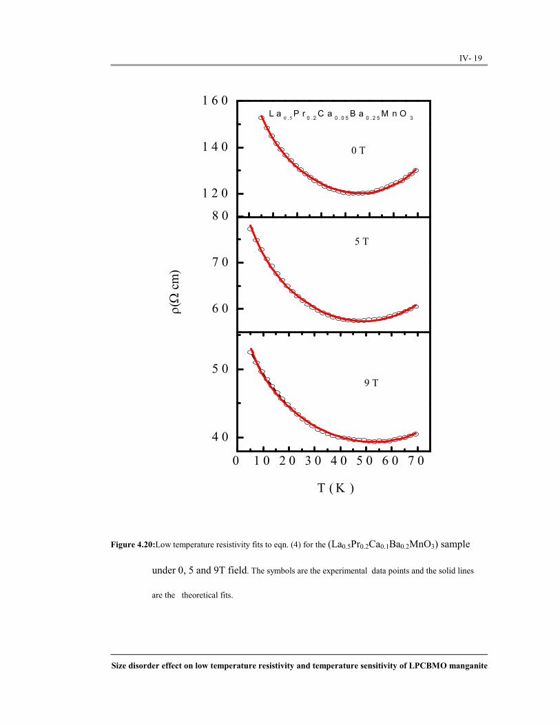
Size disorder effect on low temperature resistivity and temperature sensitivity of LPCBMO manganite
IV- 19
1 2 0
1 4 0
1 6 0
6 0
7 0
8 0
0 1 0 2 0 3 0 4 0 5 0 6 0 7 0
4 0
5 0
L a0 . 5P r
0 .2C a
0 . 0 5B a
0 . 2 5M n O
3
T ( K )
ρ(Ω
cm
)
0 T
5 T
9 T
Figure 4.20:Low temperature resistivity fits to eqn. (4) for the (La0.5Pr0.2Ca0.1Ba0.2MnO3) sample
under 0, 5 and 9T field. The symbols are the experimental data points and the solid lines
are the theoretical fits.

Size disorder effect on low temperature resistivity and temperature sensitivity of LPCBMO manganite
IV- 20
1 0 0
1 2 0
1 4 0
5 0
6 0
7 0
0 1 0 2 0 3 0 4 0 5 0 6 0 7 0
4 0
5 0
L a0 . 5P r
0 . 2B a
0 . 3M n O
3
T ( K )
ρ(Ω
cm
)0 T
5 T
9 T
Figure 4.21:Low temperature resistivity fits to eqn. (4) for the (La0.5Pr0.2Ba0.3MnO3) sample
under 0, 5 and 9T field. The symbols are the experimental data points and the solid lines
are the theoretical fits.
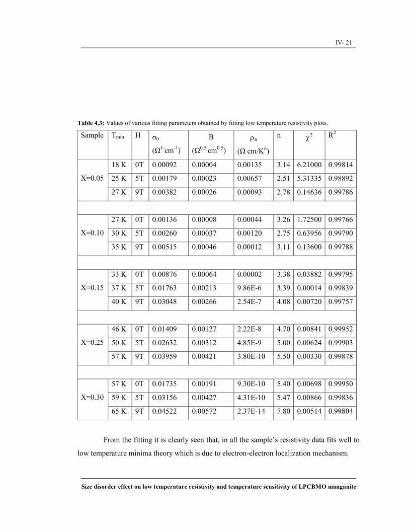
Size disorder effect on low temperature resistivity and temperature sensitivity of LPCBMO manganite
IV- 21
Table 4.3: Values of various fitting parameters obtained by fitting low temperature resistivity plots.
Sample Tmin H σ0
(Ω1-cm-1)
B
(Ω0.5 cm0.5)
ρn
(Ω cm/Kn)
n χ2
R2
18 K 0T 0.00092 0.00004 0.00135 3.14 6.21000 0.99814
25 K 5T 0.00179 0.00023 0.00657 2.51 5.31335 0.98892
X=0.05
27 K 9T 0.00382 0.00026 0.00093 2.78 0.14636 0.99786
27 K 0T 0.00136 0.00008 0.00044 3.26 1.72500 0.99766
30 K 5T 0.00260 0.00037 0.00120 2.75 0.63956 0.99790
X=0.10
35 K 9T 0.00515 0.00046 0.00012 3.11 0.13600 0.99788
33 K 0T 0.00876 0.00064 0.00002 3.38 0.03882 0.99795
37 K 5T 0.01763 0.00213 9.86E-6 3.39 0.00014 0.99839
X=0.15
40 K 9T 0.03048 0.00266 2.54E-7 4.08 0.00720 0.99757
46 K 0T 0.01409 0.00127 2.22E-8 4.70 0.00841 0.99952
50 K 5T 0.02632 0.00312 4.85E-9 5.00 0.00624 0.99903
X=0.25
57 K 9T 0.03959 0.00421 3.80E-10 5.50 0.00330 0.99878
57 K 0T 0.01735 0.00191 9.30E-10 5.40 0.00698 0.99950
59 K 5T 0.03156 0.00427 4.31E-10 5.47 0.00866 0.99836
X=0.30
65 K 9T 0.04522 0.00572 2.37E-14 7.80 0.00514 0.99804
From the fitting it is clearly seen that, in all the sample’s resistivity data fits well to
low temperature minima theory which is due to electron-electron localization mechanism.

Size disorder effect on low temperature resistivity and temperature sensitivity of LPCBMO manganite
IV- 22
From the table, one can see that χ2 is below the 1, accept x = 1.0 sample, in that it is
little higher, which shows the good quality of fitting χ2 decrease sharply with increasing size
disorder which denotes that low temperature minima is increase with Ba concentration and
with increasing size disorder, it fit our theoritical model very perfectly. From the fitting plots
and table 4.3, it is seen that for all the sample, Tmin is present means this effect is not due to
impurity (magnetic or non magnetic). So we have ruled out the kondo effect in our bulk
samples. We believe that Tmin is the temperature beyond which the increase in ρ due to the
electron-electron interaction is essentially due to the increase of coefficient B with the field
and hence Tmin moves to higher temperature. However, effect of field on TIm is not yet clear.
0.05 0.10 0.15 0.20 0.25 0.3015
20
25
30
35
40
45
50
55
60
La0.5
Pr0.2
Ca0.3-x
BaxMnO
3
Tm
in
Concentration
Figure 4.22: Concentration Vs Tmin plot for the La0.5Pr0.2Ca0.3-xBaxMnO3
(x = 0.05 to 0.3) samples

Size disorder effect on low temperature resistivity and temperature sensitivity of LPCBMO manganite
IV- 23
0.05 0.10 0.15 0.20 0.25 0.30
0.000
0.002
0.004
0.006
0.008
0.010
0.012
0.014
0.016
0.018La
0.5Pr
0.2Ca
0.3-xBa
xMnO
3
Res
idua
l Res
isti
vity
Concentration
Figure 4.23: Concentration Vs. residual resistivity plot for the La0.5Pr0.2Ca0.3-xBaxMnO3
(x = 0.05 to 0.3) samples
To see the effect of the size variation on the low temperature minima, we have plot
the concentration Vs. Tmin. and concentration Vs. residual resistivity plots which shown as
a figure 4.22 and 4.23.
Now from the figure 4.22, it is clearly seen that temperature Tmin increase as
concentration of Ba increases in the sample means temperature of Tmin increasing with size
disorder, simultaneously residual resistivity also increasing with the size disorder which is
shown in the figure 4.23. So from the table 4.3 and figures 4.22 and 4.23, it can be said
that as size disorder increase role of elastic scattering become dominant. This may be
understood in term of electron localization, as size disorder increase, modify the angle
between Mn-O-Mn bond angle. At low temperature in the absence of thermal activation
energy, spin are localize at Mn orbits and resistivity shows the upturn in its nature.

Size disorder effect on low temperature resistivity and temperature sensitivity of LPCBMO manganite
IV- 24
4.4 Temperature sensitivity (TCR) study
Uncooled infrared imaging systems based on microbolometers offers the possibility
for the development of a light weight, inexpensive alternative for complex, cooled IR
imagining systems based on the HgCdTe (MCT) or InSb . The sensitivity of presently used
microbolometer based systems is one order of magnitude lower than that of
semiconducting systems. The active element in the microbolometer based detector is an
oxide-coated silicon micro-bridge. The oxide film has a temperature-dependent resistance.
Heating of the micro-bridge by the incident IR radiation is detected by a change in the
micro bridge resistivity[20-22].
Due to the advances in thermoelectric cooling, materials with high thermal
nonlinearities in the temperature range of 250-300 K, are potential candidates for
bolometric sensors. The figure of merit for a bolometric material is the thermal coefficient
of resistance (TCR) and the noise volume (S)[22]. The commercial bolometers based on
VOx today use TCR values around 2.5-4%. In comparison TCR values ranging from 8 to
18% are possible in the manganites LCMO over the very same temperature range. The
TCR is very closely related to the magnetic homogeneity of the material and as a matter of
fact that there is strong correlation between TCR and the thermal coefficient of the
magnetization (TCM), the inverse ferromagnetic resonance (FMR) line width and the
value of the total magnetization. The TCR value drops with the increase in the Curie
temperature, which is an indication of an intrinsic thermal inhomogeneity in these
manganites. Early noise measurements in the manganites also showed very large noise
volumes in those materials which were typically four to six orders of magnitude larger
than was seen in other metal oxide conductors such as YBCO. However, recently, we are
seeing significantly reduced noise volumes in higher quality manganite films and there is a
clear correlation with increased TCR values. Noise characteristics of CMR already
reported in comparison with other oxide conductors such as YBCO. The films made
today with much higher TCR values also show two orders of magnitude reduction in the
noise volumes. The discovery of new materials with higher TCR would increase the
sensitivity of the microbolometers comparable with MCT detectors[23].
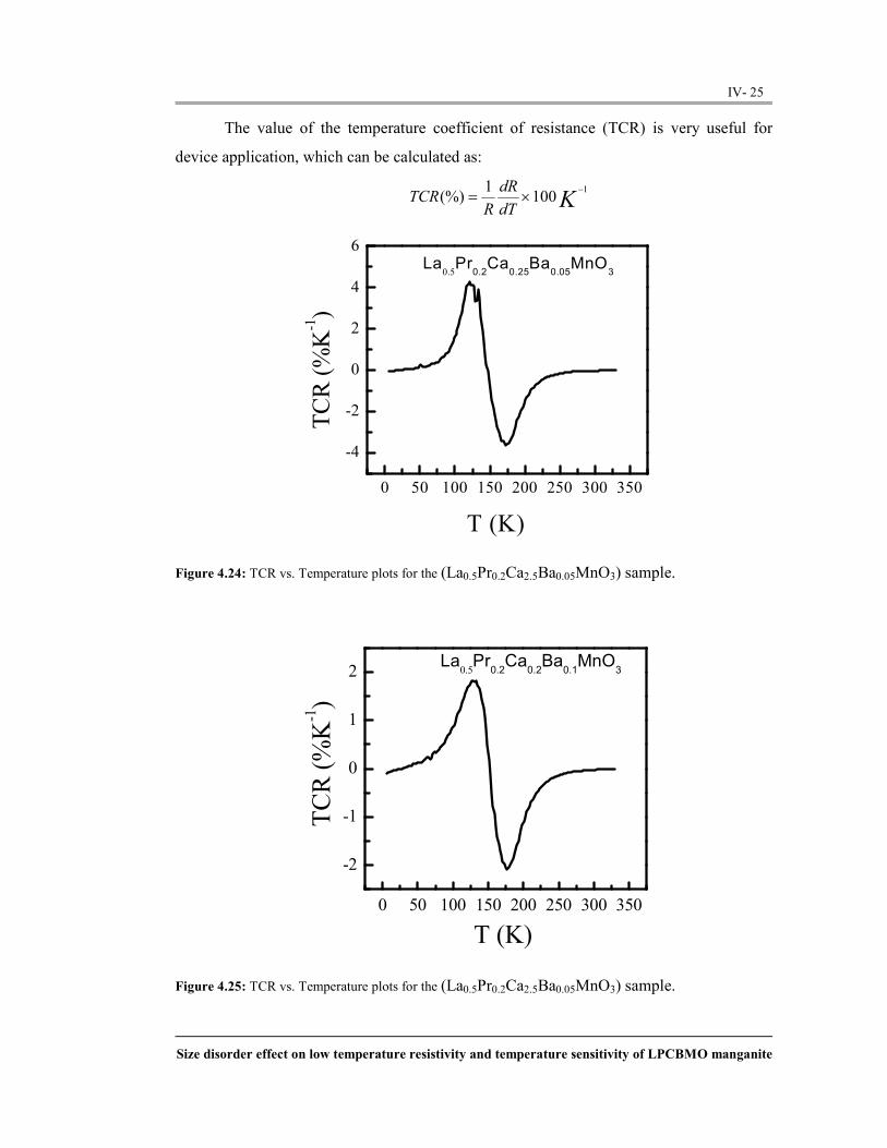
Size disorder effect on low temperature resistivity and temperature sensitivity of LPCBMO manganite
IV- 25
The value of the temperature coefficient of resistance (TCR) is very useful for
device application, which can be calculated as:
KdT
dR
RTCR
1100
1(%)
−×=
0 50 100 150 200 250 300 350
-4
-2
0
2
4
6La
0.5Pr
0.2Ca
0.25Ba
0.05MnO
3
TC
R (
%K
-1)
T (K)
Figure 4.24: TCR vs. Temperature plots for the (La0.5Pr0.2Ca2.5Ba0.05MnO3) sample.
0 50 100 150 200 250 300 350
-2
-1
0
1
2La
0.5Pr
0.2Ca
0.2Ba
0.1MnO
3
TC
R (
%K
-1)
T (K)
Figure 4.25: TCR vs. Temperature plots for the (La0.5Pr0.2Ca2.5Ba0.05MnO3) sample.

Size disorder effect on low temperature resistivity and temperature sensitivity of LPCBMO manganite
IV- 26
0 50 100 150 200 250 300 350-2.0
-1.5
-1.0
-0.5
0.0
0.5
1.0
1.5
2.0La
0.5Pr
0.2Ca
0.15Ba
0.15MnO
3
TC
R (
%K
-1)
T (K)
Figure 4.26: TCR vs. Temperature plots for the (La0.5Pr0.2Ca2.5Ba0.05MnO3) sample.
0 50 100 150 200 250 300 350
-1.5
-1.0
-0.5
0.0
0.5
1.0La
0.5Pr
0.2Ca
0.05Ba
0.25MnO
3
TC
R (
%K
-1)
T (K)
Figure 4.27: TCR vs. Temperature plots for the (La0.5Pr0.2Ca2.5Ba0.05MnO3) sample.
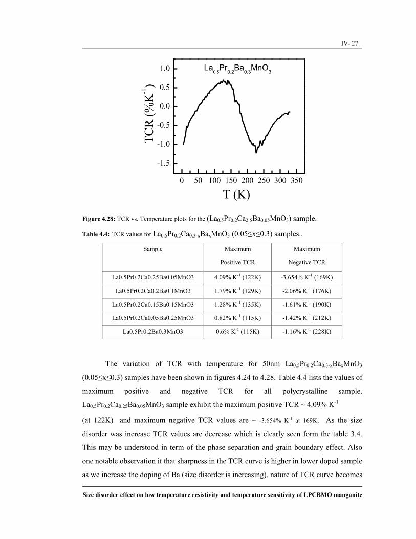
Size disorder effect on low temperature resistivity and temperature sensitivity of LPCBMO manganite
IV- 27
0 50 100 150 200 250 300 350
-1.5
-1.0
-0.5
0.0
0.5
1.0 La0.5Pr
0.2Ba
0.3MnO
3
TC
R (
%K
-1)
T (K)
Figure 4.28: TCR vs. Temperature plots for the (La0.5Pr0.2Ca2.5Ba0.05MnO3) sample.
Table 4.4: TCR values for La0.5Pr0.2Ca0.3-xBaxMnO3 (0.05≤x≤0.3) samples..
Sample Maximum
Positive TCR
Maximum
Negative TCR
La0.5Pr0.2Ca0.25Ba0.05MnO3 4.09% K-1 (122K) -3.654% K-1 (169K)
La0.5Pr0.2Ca0.2Ba0.1MnO3 1.79% K-1 (129K) -2.06% K-1 (176K)
La0.5Pr0.2Ca0.15Ba0.15MnO3 1.28% K-1 (135K) -1.61% K-1 (190K)
La0.5Pr0.2Ca0.05Ba0.25MnO3 0.82% K-1 (115K) -1.42% K-1 (212K)
La0.5Pr0.2Ba0.3MnO3 0.6% K-1 (115K) -1.16% K-1 (228K)
The variation of TCR with temperature for 50nm La0.5Pr0.2Ca0.3-xBaxMnO3
(0.05≤x≤0.3) samples have been shown in figures 4.24 to 4.28. Table 4.4 lists the values of
maximum positive and negative TCR for all polycrystalline sample.
La0.5Pr0.2Ca0.25Ba0.05MnO3 sample exhibit the maximum positive TCR ~ 4.09% K-1
(at 122K) and maximum negative TCR values are ~ -3.654% K-1 at 169K. As the size
disorder was increase TCR values are decrease which is clearly seen form the table 3.4.
This may be understood in term of the phase separation and grain boundary effect. Also
one notable observation it that sharpness in the TCR curve is higher in lower doped sample
as we increase the doping of Ba (size disorder is increasing), nature of TCR curve becomes

Size disorder effect on low temperature resistivity and temperature sensitivity of LPCBMO manganite
IV- 28
more border. In the last sample of this series La0.5Pr0.2Ba0.3MnO3 exhibit very large
broadening effect in the TCR curves. This behavior also observed in the R-T plots of
La0.5Pr0.2Ca0.3-xBaxMnO3 (0.05≤x≤0.3) samples.
This anomaly is not in accordance with the Zener-Double-Exchange interactions
and can be explained on the purview of possible grain boundary localization or phase
separation. It is needless to mention that the polycrystalline samples of various micron
sized grains, in which properties may vary inside the grain and on the grain boundaries. As
the ZDE come into play, the bulk part of the grain become ferromagnetic and metallic
while the grain boundaries are still insulating. The grain boundaries may be insulating
because of the grain boundary pinning of Mn-ion spins, poor connectivity and grain
boundary contamination. This creates the insulating channels at the grain boundaries and
does not allow the percolation of the charge carriers and results in insulating behavior even
after the onset of TC. Once the grain boundaries become conducting at lower temperatures,
the I-M transitions appear. Other factor that can cause a disparity between the shaper TCR
curve in lower size disorder sample and border TCR curve in large size disorder sample is
due to the phase-separation. Due to the granular mixture of different electronic densities,
the TC of different grains could be different. For instance, we assume that majority of the
grains have large electronic density so that they exhibit TC at higher temperatures, while
the remaining minor fraction have lower TC. Now, at the onset of the TC of majority of
grains (with higher TC), the systems tends to be ferromagnetic even as a minority of grain
are still paramagnetic-insulating. In such as a situation, though the system will be
ferromagnetic, it will continue to exhibit semiconducting/insulating behavior unless all the
grains become ferromagnetic. At a certain temperature when the whole system attains
ferromagnetism, percolation is possible and the system exhibits I-M transition.
4.5 Conclusion
The XRD pattern of all the La0.5Pr0.2Ca0.3-xBaxMnO3 (x = 0.05 to 0.3) samples are
single phasic in nature and in these samples cell volume increase with increase in size
disorder (Ba+2 concentration). After rietveld analysis of these sample we have identified
that these samples have distorted orthorhombic structure. From the electrical resistivity
measurement we can clearly observed that the low temperature minima below 50 K. Also

Size disorder effect on low temperature resistivity and temperature sensitivity of LPCBMO manganite
IV- 29
broadening in peak resistivity with increasing size disorder can be explain in terms of
phase separation come into picture due to grain boundary effect. Also an enhancement in
the temperature of Tp with increasing size disorder may be explain in term of
modification in Mn-O-Mn bond angle which favouring the ferromagnetism.
To see the size disorder effect in low temperature resistivity minima, we have try to
feet various theoretical model in the low temperature range, such as electron-electron
scattering, magnon scattering, bulk scattering model including quantum correction to
concuctivity but in our samples low temperature resistivity fit very nicely with the
combination of ρelastic and ρinelastic terms (
n
nT
BTρ
σρ +
+=
2/10
1
).
After the fitting of the resistivity data in above equation, we can conclude that size
disorder dramatically affect the low temperature minima. With increasing size disorder
temperature of Tmin and residual resistivity increase exhibit the role of elastic scattering.
Contribution of elastic scattering is higher in the large distorted sample which is
La0.5Pr0.2Ba0.3MnO3. This disorder localize the spin at low temperature in distorted lattice
which resulting into resistivity upturn.
From the study of temperature sensitivity of La0.5Pr0.2Ca0.3-xBaxMnO3 (x = 0.05 to
0.3) samples, we have observed that TCR value decrease with increasing size disorder, this
may be understood in term of increasing in ferromagnetic phase near Tc with increasing
Ba concentration like as in the electronic transport.

Size disorder effect on low temperature resistivity and temperature sensitivity of LPCBMO manganite
IV- 30
REFERENCES
1. M. N. Baibich, J. M. Broto, F. Nguyen Van Daw, F. Petroff, P. Etienne, G.
Crevzet, A. Friederich and J. Chazelas
Phys. Rev. Lett. 61 2472 (1988).
2. A. P. Ramirez
J. Phys.: Condens. Matter. 9 8171 (1997).
3. B. Reveau, A. Maignan, C. Martin and M. Hervieu
“Colossal Magnetoresistance, Charge Ordering and Related properties of
manganites
Oxides” ed:by C. N. R. Rao and B. Raveau
(Singapore: word scientific) P 43, P 83, (1998).
4. M. Viret, L. Ranno and J. M. D. Coey
Phys. Rev. 55 8067 (1997).
5. P. Raychaudhuri, T. K. Nath, A. K. Nigam and R. Pinto
J. Appl. Phys. 84 2048 (1998).
6. A. Gupta and J. Z. Sun
J. Magn. Magn. Mater. 200 24 (1999).
7. J. M. D. Coey, M. Viret, L. Ranno and K. Ounadjela
Phys. Rev. Lett. 75 3910 (1995).
8. Ph.D Thesis of C. M. Thaker (2007).
9. N. Furukawa: “Physics of Manganites” edited by T. Kaplan and S. Mahanti
(Plenum Publishing, New York, 1999).
10. Nobuo Furukawa
J. Phys. Soc. Jap. 69 1954 (2000).
11. M. B. Salamon and M. Jaime
Rev. Mod. Phys. 73 602 (2001).
12. K. Kubo and N. Ohata
J. Phys. Soc. Jpn. 33 21 (1972).
13. Xindong Wang and X. G. Zhang
Phys. Rev. Lett. 82 4276 (1999).

Size disorder effect on low temperature resistivity and temperature sensitivity of LPCBMO manganite
IV- 31
14. T. Akimoto, Y. Moritomo, A. Nakamura, N. Furukawa
Phys. Rev. Lett. 85 3914 (2000).
15. S. K. Singh, S. B. Palmer, D. M. Paul and M. K. Lees
Appl. Phys. Lett. 69 263 (1996).
16. D. K. Petrov, L. Krusin-Elabaum, J. Z. Sun, C. Field and P. R. Duncombe
Appl. Phys. Lett. 75 995 (1999).
17. A. Tiwari and K. P. Rajeev
Solid State Commun. 111 33 (1999).
18. D. S. Rana, J. H. Markna, R. N. Parmar, D. G. Kuberkar, P. Raychaudhuri, J. John
and S. K. Malik
Phys. Rev. B 71 1 (2005).
19. B. L. Altshuler and A. G. Aronov
In electron-electron Interactions in Disordered System, edited by A. L. Efros and
M. Pollak (North-Holland, Amsterdam) (1985).
20. M. Rajeswari, C. H. Chen, A. Goyal, C. Kwo, M. C. Robson, R. Ramesh,
T. Venkatesan and S. Lakeou.
Appl. Phys. Lett. 68 3555 (1996).
21. S. B. Ogale, R. Shreekala, R. Bathe, S. K. Date, S. I. Patil, B. Hannoyer, F. Petit
and G. Marest
Phys. Rev. B 57 7841 (1998).
22. Ravi Kumar, R. J. Choudhary, S. I. Patil, Shahid Hussain, J. P. Srivastava and
S. K. Malik
Appl. Phys. Lett. 86 222501 (2005).
23. J. H. Markna, R. N. Parmar, D. G. Kuberkar, Ravi Kumar, D. S. Rana and
S. K. Malik
Appl. Phys. Lett. 88 152503 (2006).

Chapter - 5

Studies on Chemical Solution Deposited LPSMO Manganite Series
V - 1
5.1 Introduction
Mixed valent manganites with the perovskite structure have been studied for
almost 50 years. The system offers a degree of chemical flexibility which permits the
relation between the oxides’ structure, electronic and magnetic properties to be examined
in a systematic way. Research on the manganites has revealed new phenomena such as
colossal [1] and dense granular magnetoresistance [2], and has led to the formulation of
important physical concepts such as double exchange. The experiments performed on
polycrystalline samples showed antiferromagnetic (AF) insulating behavior at low and
high concentration (x) values and show Ferromagnetic-Paramagnetic transition (Tc)
followed by the Metal-Insulator transition (Tp) in a certain range of concentrations
centered around x =1/3 [1-3]..
This striking behavior was early explained by Zener in the theory of double-
exchange (DE) [4]. Since 1993, an enormous amount of work has been devoted to the
mixed-valence oxides, mainly to the manganites RE1-xMxMnO3 (RE = rate earth, M = Ca,
Sr, Ba, Pb) with three-dimensional perovskite type structure. The investigations have been
carried out on polycrystalline sintered samples, single crystals and thin films.The last
decade had seen the emergence of epitaxial metal oxide films as one of the most attractive
subjects for the condensed matter community. The emergence of such interest was
primarily stimulated by the discovery of the colossal-magnetorestance (CMR) effect in
thin films of manganese oxides RE1-xMxMnO3. CMR materials exhibit large changes in
electrical resistance when an external magnetic field is applied. The physical properties of
perovskite-type manganites are determined by two main parameters: the doping level, x=
Mn4+
/(Mn3+
+ Mn4+
), and the average size of the cation A, <rA>. A third relevant
parameter is the degree of disorder at site A, defined by σ2 = r
2A - <rA>
2. The compound
RE1-xMxMnO3 exhibits a variety of phases when the carrier concentration (x) and
temperature (T) are varied. These phases are characterized by different magnetic and
transport properties [5].
The phase diagram and low-temperature behavior of La1-xSrxMnO3 (LSMO) shows
that there are some differences in its phase diagram than that of PCMO mainly due to the
size difference between Pr, Ca and Sr ions, Sr being quite larger in size as compared to Pr
and Ca. It is reported that, there are three distinct ground states, the spin-canted insulator,
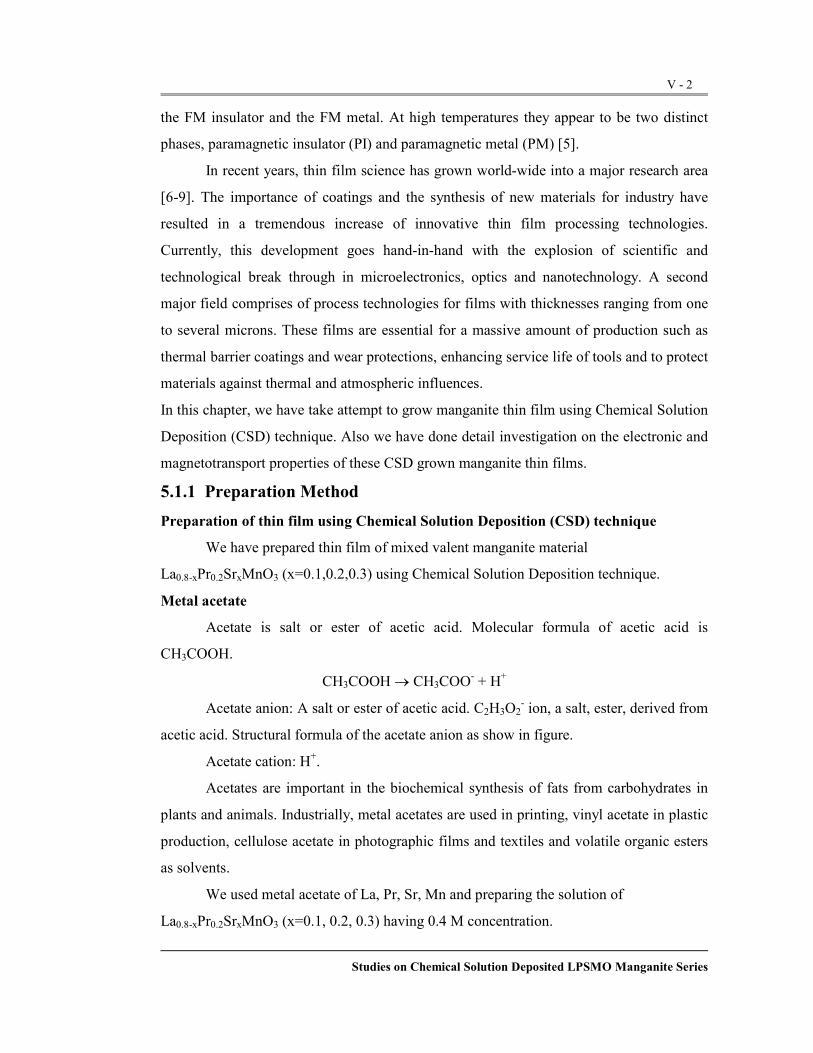
Studies on Chemical Solution Deposited LPSMO Manganite Series
V - 2
the FM insulator and the FM metal. At high temperatures they appear to be two distinct
phases, paramagnetic insulator (PI) and paramagnetic metal (PM) [5].
In recent years, thin film science has grown world-wide into a major research area
[6-9]. The importance of coatings and the synthesis of new materials for industry have
resulted in a tremendous increase of innovative thin film processing technologies.
Currently, this development goes hand-in-hand with the explosion of scientific and
technological break through in microelectronics, optics and nanotechnology. A second
major field comprises of process technologies for films with thicknesses ranging from one
to several microns. These films are essential for a massive amount of production such as
thermal barrier coatings and wear protections, enhancing service life of tools and to protect
materials against thermal and atmospheric influences.
In this chapter, we have take attempt to grow manganite thin film using Chemical Solution
Deposition (CSD) technique. Also we have done detail investigation on the electronic and
magnetotransport properties of these CSD grown manganite thin films.
5.1.1 Preparation Method
Preparation of thin film using Chemical Solution Deposition (CSD) technique
We have prepared thin film of mixed valent manganite material
La0.8-xPr0.2SrxMnO3 (x=0.1,0.2,0.3) using Chemical Solution Deposition technique.
Metal acetate
Acetate is salt or ester of acetic acid. Molecular formula of acetic acid is
CH3COOH.
CH3COOH → CH3COO- + H
+
Acetate anion: A salt or ester of acetic acid. C2H3O2- ion, a salt, ester, derived from
acetic acid. Structural formula of the acetate anion as show in figure.
Acetate cation: H+.
Acetates are important in the biochemical synthesis of fats from carbohydrates in
plants and animals. Industrially, metal acetates are used in printing, vinyl acetate in plastic
production, cellulose acetate in photographic films and textiles and volatile organic esters
as solvents.
We used metal acetate of La, Pr, Sr, Mn and preparing the solution of
La0.8-xPr0.2SrxMnO3 (x=0.1, 0.2, 0.3) having 0.4 M concentration.

Studies on Chemical Solution Deposited LPSMO Manganite Series
V - 3
Preparation of precursor solution
Stoichiometric amounts of starting materials were dissolved in 2.5 ml acetic acid
and 2.5 ml distilled water to yield solution having perfect stoichiometry.
Such solution was heated to ∼ 100°C for few minute to dissolve precursor (if there)
and uniform solution was obtained was kept at 350°C for 30 minute for the calcination
process.
Substrate
The subtrate used was single crystal LaAlO3(LAO). Single crystal provides a good
lattice match to perovskite structured materials.
Deposition of solution using automatic spin coater
Spin coating
Spin coating is a procedure used to apply uniform thin films to flat substrates. In
short, an excess amount of the solvent is placed on the substrate, which is then rotated at
high speed in order to spread the fluid by centrifugal force. Rotation is continued while the
fluid spins off the edges of the substrate, until the desired thickness of the film is achieved.
The applied solvent is usually volatile, and simultaneously evaporates. So, the higher the
angular speed of spinning, the thinner the film. The thickness of the film also depends on
the concentration of the solution and the solvent.
Key stages in spin coating:
Step 1: The first stage is the deposition of the coating fluid onto the wafer or substrate. It
can be done using a nozzle that pours the coating solurion out, or it could be
sprayed onto the surface, etc. Usually this dispense stage provides a substantial
excess of coating solution compared to the amount that will ultimately be required
in the final coating thickness.
Step 2: The substrate is accelerated up to its final, desired, rotation speed.
Step 3: The substrate is spinning at a constant rate and fluid viscous forces dominate the
fluid thinning behaviour.
Step 4: The substrate is spinning at a constant rate and solvent evaporation dominates the
coating thinning behavior.
Speed of rotation and time period for rotation can maintained externally as per
requirement.We used, Speed:6000 RPM and Time: 25 Sec.

Studies on Chemical Solution Deposited LPSMO Manganite Series
V - 4
Annealing :
It is a process that produces equilibrium conditions by heating and maintaining at a
suitable temperature and then cooling very slowly. It is used to induce softness, relieve
internal stresses, refine the structure and improve cold working properties.
In oxygen annealing process, oxygen atmosphere is provide to the thin film.
As a final stage of preparation of thin film, oxygen annealing process was carried
out at 1100°C for 12 Hours in tube furnace.
We can maintain cooling and heating rates as per requirement in tube furnace up to
1400°C.
5.2 Structural Studies
Thin films of La0.8-xPr0.2SrxMnO3 (LPSMO) (x = 0.1, 0.2 and 0.3) were grown on
the polished (hOO) LaAlO3 (LAO) single crystal substrate. Substrate was cut in desired
manner, polished and cleaned. XRD measurements using Cu-Kα radiation were performed
on the thin film samples. The Powder X programme was employed to estimate the
structure and cell parameters of these samples. The films were deposited with film
thicknesses ∼ 150 nm. In figs. 5.1, 5.2 and 5.3, we show the XRD patterns of La0.8-
xPr0.2SrxMnO3 (x = 0.1, 0.2 and 0.3) thin films grown on the LAO substrate. From the (θ -
2θ) XRD profile it can be seen that the films are epitaxial and with out of plane orientation
confirming the growth in (00l) direction. From the XRD, we can say that the films grown
are oriented and the orientation does not match with substrates this may be due to large
different in the lattice parameter of the bulk material and film substrate. These show that
there is strain in the film although this may be sufficiently relaxed due to larger thickness.
The lattice mismatch δ along the interface has been calculated using the following
formula.
100×−
=substrate
filmsubstrate
d
ddδ
In above equation negative value of mismatch corresponds to the compressive
strain while positive value corresponds to the tensile strain [7]. Here in present case,
La0.7Pr0.2Sr0.1MnO3/LAO thin film exhibits the mismatch ∼ -3.34% while another thin
films namely La0.6Pr0.2Sr0.2MnO3/LAO and La0.5Pr0.2Sr0.3MnO3/LAO films exhibit the
mismatch ∼ -1.89% and ∼ -2.88% respectively.
Studies on Chemical Solution Deposited LPSMO Manganite Series
V - 5
20 30 40 50 601
10
100
1k
10k
100kLa
0.7Pr
0.2Sr
0.1MnO
3/LAO
(200)
(002)
(100)
(001)
Inte
nsi
ty (
a.u.)
2θ (degree)
Figure 5.1: Indexed XRD pattern of La0.7Pr0.2Sr0.1MnO3/LAO film.
20 30 40 50 601
10
100
1k
10k
100kLa
0.6Pr
0.2Sr
0.2MnO
3/LAO
(200)
(002)
(100)
(001)
Inte
nsi
ty (
a.u.)
2θ (degree)
Figure 5.2: Indexed XRD pattern of La0.6Pr0.2Sr0.2MnO3/LAO film.

Studies on Chemical Solution Deposited LPSMO Manganite Series
V - 6
20 30 40 50 601
10
100
1k
10k
100kLa
0.5Pr
0.2Sr
0.3MnO
3/LAO
(200)
(002)
(100)
(001)
Inte
nsi
ty (
a.u.)
2θ (degree)
Figure 5.3: Indexed XRD pattern of La0.5Pr0.2Sr0.3MnO3/LAO film.
5.3 Surface morphology using AFM
The surface morphology of all the La0.8-xPr0.2SrxMnO3 (LPSMO) (x = 0.1, 0.2 and 0.3)
films was studied using the AFM measurements. The pictures 5.1, 5.21 and 5.3 show the
surface topology and roughness histogram of the La0.8-xPr0.2SrxMnO3 (LPSMO) (x = 0.1,
0.2 and 0.3) films, respectively. From the AFM picture of these films, it is clearly observed
that in the all the films with have similarly grain size ~100nm. Also it clearly observed
that, films have continuous grains formation showing the good quality of the CSD grown
thin films. The surface roughness analysis of these films shows the RMS roughness ~
12.3nm, 15.7nm and 18.3nm for La0.8-xPr0.2SrxMnO3 (LPSMO) (x = 0.1, 0.2 and 0.3) thin
films, respectively. Here in the present CSD grown films RMS roughness is quite higher
than the PLD grown thin films which may be due to different growth technique.

Studies on Chemical Solution Deposited LPSMO Manganite Series
V - 7
Picture 5.1: 2D AFM image and histogram for the roughness analysis of the 150nm
La0.7Pr0.2Sr0.1MnO3/LAO thin film grown by CSD technique.
Picture 5.2: 2D AFM image and histogram for the roughness analysis of the 150nm
La0.6Pr0.2Sr0.2MnO3/LAO thin film grown by PLD technique.

Studies on Chemical Solution Deposited LPSMO Manganite Series
V - 8
Picture 5.3: 2D AFM image and histogram for the roughness analysis of the 150nm
La0.5Pr0.2Sr0.3MnO3/LAO thin film grown by CSD technique.
5.4 Electronic transport and Temperature sensitivity studies
The plots of resistivity as a function of temperature for La0.7Pr0.2Sr0.1MnO3/LAO,
La0.6Pr0.2Sr0.2MnO3/LAO and La0.5Pr0.2Sr0.3MnO3/LAO thin films in zero field and 0.7 T
fields over temperature range of 130 K to 320 K are show in figs. 5.4 to 5.6. Figure 5.4
shows the TIM ~ 221K for the La0.7Pr0.2Sr0.1MnO3/LAO films while TIM ~333K & ~ 365K
for La0.6Pr0.2Sr0.2MnO3/LAO and La0.5Pr0.2Sr0.3MnO3/LAO, respectively.
It can be observed that, TIM increases with Sr concentration from 221K to 365 K.
Also, from these resistivity plots, one can say that, as we increase the Sr concentration,
resistivity decreases sharply in all films. It is notable that, the CSD grown thin films show
very good agreement in TIM values for bulk samples [5]. This resistivity plots provide
experimental evidence of good quality of thin film which is first time grown by the CSD
technique.

Studies on Chemical Solution Deposited LPSMO Manganite Series
V - 9
Figure 5.4: Resistivity vs. Temperature plots of La0.7Pr0.2Sr0.1MnO3/LAO thin films at
H=0 and 0.7T.
Figure 5.5: Resistivity vs. Temperature plots of La0.6Pr0.2Sr0.2MnO3/LAO thin films at
H=0 and 0.7T.

Studies on Chemical Solution Deposited LPSMO Manganite Series
V - 10
Figure 5.6: Resistivity vs. Temperature plots of La0.5Pr0.2Sr0.3MnO3/LAO thin films at
H=0 and 0.7T.
5.5 Magnetotransport properties
The resistance was measured as a function of temperature in 0.7 applied magnetic
field for all La0.8-xPr0.2SrxMnO3 (x = 0.1, 0.2 and 0.3) thin films grown on the LAO
substrates. From these data, magneto resistance(MR) was calculated using the formula
MR(%)=(ρ0-ρH)/ρ0×100 and the plots of MR vs T are shown in figs. 5.7 to 5.9. It may
be seen that, all the samples exhibit maximum MR in the vicinity of their respective I-M
transition temperatures. Maximum MR in the vicinity of TIM may be explained on the
basis of field induced suppression of spin fluctuation. At the I-M transition, there exists
maximum magnetic disorder and magnetic field enhances the ferromagnetic spin ordering.
Here as shown in the magnetoresistance plot, La0.7Pr0.2Sr0.1MnO3/LAO thin film exhibits
the MR% ~ 25 at TIM while La0.6Pr0.2Sr0.2MnO3/LAO and La0.5Pr0.2Sr0.3MnO3/LAO thin
Studies on Chemical Solution Deposited LPSMO Manganite Series
V - 11
films MR% is ~ 9% and 10%, respectively. Hence we can say that, MR % decreases as Sr
concentration is increased which indicates that the ferromagnetic phase increases in the
sample with Sr concentration which is responsible for the decrease in the
magnetoresistance at TIM. In the La0.5Pr0.2Sr0.3MnO3/LAO thin films exhibit ~ 10%
magnetoresistance in the vicinity of the RT in 0.7 Tesla applied field which shows that the
film has application potential in thin film devices such as field sensor (figure 5.9).
On the other hand, at low temperature, MR is due to grain boundary effect which is
explained by the inter-grain spin-polarized tunneling mechanism. From the
magnetoresistance plots we can observe that, in the present case magnetoresistance is very
small at the low temperature below the TIM in the metallic region. This may be understood
in the term of grain boundary effect. In the epitaxially grown thin films all the grains are
in single direction oriented and the magnetic domain also is in single direction so as the
application of magnetic field does not change in the resistivity appreciably and hence
observed magnetoresistance is very small as compared to that of in the bulk sample.

Studies on Chemical Solution Deposited LPSMO Manganite Series
V - 12
Figure 5.7: MR vs. Temperature plot of La0.7Pr0.2Sr0.1MnO3/LAO thin film.
Figure 5.8: MR vs. Temperature plot of La0.6Pr0.2Sr0.2MnO3/LAO thin film.

Studies on Chemical Solution Deposited LPSMO Manganite Series
V - 13
Figure 5.9: MR vs. Temperature plot of La0.5Pr0.2Sr0.3MnO3/LAO thin film.
5.6 Conclusion
In this chapter, we have successfully grown the thin films of La0.8-xPr0.2SrxMnO3
manganite on single crystal LAO substrates using chemical solution deposition technique.
Here, all grown thin films possess thickness of ~150nm and are oriented in (00l) direction.
All the films are epitaxial in nature and growth direction is in opposite direction of
substrate. The structural study obtained from the XRD analysis shows that, the cell
parameter increases with increase of Sr2+
in these compounds and the strain effect is
present at interface in the dead layer. The surface morphology study using AFM suggests
the surface roughness ∼ 12-18 nm and the average grain size ∼ 100 nm.
The ρ-T and Magneto ρ-T behavior of the films studied show the increase of I-M
transition and decrease of ρpeak with the increasing Sr (x) concentration. It is evident from
the MR Vs. T(K) plots that, the Maximum MR ∼ 25% (∼200 K) is obtained for the
minimum Sr concentration (x = 0.1). The increasing hole concentration (x) results into the
lowering of MR which is ∼ 10% (∼ 350 K) for x = 0.3.

Studies on Chemical Solution Deposited LPSMO Manganite Series
V - 14
The comparison of the presently obtained results on the structure, surface
morphology, transport and magnetotransport properties of CSD grown LPSMO films with
those of earlier reported results on La0.5Pr0.2Sr0.3MnO3 film grown by PLD technique [11]
shows the following interesting aspects of the study.
La0.5Pr0.2Sr0.3MnO3 CSD PLD [ref.11]
Strain -2.88 % -2.64 %
RMS roughness 18.3 nm 1.9 nm
TIM 365 K 328 K
ρpeak 9 mΩ 300 mΩ
LTMR 0.4 % 1 %
HTMR 10 % 9 %
Based on the above mentioned comparative study, it can be concluded that, the
quality of CSD grown LPSMO films is very good with crystallographically single phase
epitaxial nature. In the case of CSD grown films, RMS roughness is higher than PLD
grown films, while strain is almost same in both the cases. Comparison of ρ-T results on
La0.5Pr0.2Sr0.3MnO3 thin films grown using CSD and PLD techniques, shows that, TIM is
higher with lower peak resistivity in the CSD grown films as compared to PLD grown
films confirming good quality of CSD grown manganite films. LTMR is very small in the
case of CSD grown films as compared to PLD grown films showing the better magnetic
homogeneity in the film, while there is no appreciable difference in HTMR values in
LPSMO films grown by PLD and CSD techniques.
In conclusion, it is possible to grow the good quality of manganite thin films
having epitaxial nature using simple and cost effective chemical solution deposition
technique having better physical properties as compared to PLD technique.

Studies on Chemical Solution Deposited LPSMO Manganite Series
V - 15
Reference
1. A. P. Ramirez.
J. Phys.: condens. Matter 9, 8171 (1997).
2. J. M. D. Coey and M. Viret.
Adv. Phys. 48, 167 (1999).
3. E. Doggoto, T. Hotta and A. Moreo.
Physics Report 344, 1 (2001).
4. C. P. Zener.
Phys. Rev. 82, 403 (1951).
5. Colossol Magnetoresistance, Charge Ordering and related properties of Manganese
Oxides Ed. By. C.N.R. Rao, B. Raveau. World Scientific Publishing Co. Pte. Ltd.
(1998).
6. M. Rajeswari, C. H. Chen, A. Goyal, C. Kwo, M. C. Robson, R. Ramesh,
T. Venkatesan, and S. Lakeou.
Appl. Phys. Lett. 68, 3555 (1996).
7. J. H. Markna, R. N. Parmar, D. G. Kuberkar, Ravi Kumar, D. S. Rana and
S. K. Malik.
Appl. Phys. Lett. 88, 152503 (2006).
8. R. Von Helmolt, J. Wecker, B. Holzapfel and L. Schultz.
Phys. Rev. Lett. 71, 2231 (1993).
9. J. A. Thornton.
J. Vac. Sci. Technol. A 4, 3059 (1986).
10. J. Z. Sun, D. W. Abraham, R. A. Rao and C. B. Eom.
Appl. Phys. Lett. 74, 3017 (1999).
11. Ph.D. Thesis of J. H. Markna (2007)

List of Publications in International/National/Conferences/Symposia/Workshop
1. “Effect of SHI irradiation on low temperature resistivity of LCMO
manganite thin films”
Communicated to Journal of Material Letters.
2. “Comparative studies on the Pulsed Laser Deposited (PLD) and Chemical Solution
Deposition (CSD) grown manganite thin films”
Communicated to Journal of Solid State Communication
CONFERENCES ATTENDED
1. One Day National Seminar on RECENT TRENDS IN MATERIALS
SCIENCE organized at Department of Physics, Saurashtra University, Rajkot
and conducted under UGC-Special Assistance Programme on March, 25th 2007.
2. DAE-BRNS 4TH National Symposium on PULSED LASER DEPOSITION OF
THINFILM AND NANOSTRUCTURED MATERIALS, PLD-2007, during
October 3-5,2007, Saurashtra University, Rajkot-360 005