saa7378gp single chip digital servo processor and compact disc
TRANSCRIPT

Preliminary specification: Version 1.0 May1995
Data Sheet
SAA7378GP
Single Chip Digital Servo Processorand Compact Disc Decoder
(CD7)
Philips Semiconductors
INTEGRATED CIRCUITS

Philips Semiconductors Preliminary specification: Version 1.0
May 1995 2
Digital Servo Processor and Compact Disc Decoder (CD7) SAA7378GP
1. FEATURES
• Single speed mode.• Full error correction strategy, t = 2 and e = 4.• All standard decoder functions implemented digitally on chip.• FIFO overflow concealment for rotational shock resistance.• Digital audio interface (EBU), audio only.• 2 - 4 times oversampling integrated digital filter.• Audio data peak level detection.• Kill interface for DAC deactivation during digital silence.• All TDA1301 (DSIC2) digital servo functions, plus extra hi-level functions.• Low focus noise.• Communication via TDA1301/SAA7345 compatible bus.• On chip clock multiplier allows the use of 8.4672MHz crystal.
2. GENERAL DESCRIPTION
CD7 (SAA7378GP) is a single chip combining the functions of a CD decoder IC and Digital Servo IC. Thedecoder part is based on CD6 (SAA7345GP) with an improved error correction strategy; the servo part is basedon DSIC2 (TDA1301T) with improvements incorporated.
3. QUICK REFERENCE DATA
4. ORDERING INFORMATION
Note1. When using reflow soldering it is recommended that the Dry Packing instructions in the " Quality Reference Pocketbook"
are followed. The pocketbook can be ordered using the code 9398 510 34011.
Supply of this Compact Disc IC does not convey an implied license under any patent right to use this IC in any Compact Discapplication.
SYMBOL PARAMETER MIN TYP MAX UNIT
VDD supply voltage 3.4 5.0 5.5 V
IDD supply current - 49 - mA
fXTAL crystal frequency 8 8.4672 35 MHz
Tamb operating ambient temperature 5 - +70 °CTstg storage temperature -55 - +125 °C
EXTENDEDTYPE NUMBER
PACKAGE
PINS PIN POSITION MATERIAL CODE
SAA7378GP 64 QFP plastic SOT393-1
Philips Semiconductors Preliminary specification: Version 1.0
May 1995 3
Digital Servo Processor and Compact Disc Decoder (CD7) SAA7378GP
VS
S4
VS
SA
1
IREF
ISLICE
HFREF
HFINDIGITAL
PLL
DEMODULATOR
EFM
CRIN
CROUT
CL11
CL16
TEST5
TIM
ING
SCL
SDA
RAB
MICRO-PROCESSOR
DOBM
SRAM
RAM
ADDRESSER
VERSATILE PINS
INTERFACE
AUDIO
PROCESSOR
KILL
PEAKDETECT
MOTOR
CONTROL
ERROR
CORRECTOR
INT
ER
FAC
E
EB
U
INT
ER
FAC
E
FLAGSTEST
TEST1
TEST2
RESET
MOTO1
MOTO2
CFLG
SCLK
WCLK
DATA
TEST8
KIL
L
V1 V2 V3 V4 V5
VR
L
D1
FR
ON
T E
ND
SE
RIA
L D
ATA
TEST10
D2
D3
D4
ADC PRE-PROCESSING
VREFGENERATOR
CONTROLFUNCTION
CONTROL
PART
OU
TP
UT
STA
GE
S
MICROPROCESSOR
INTEFACE
DECODER
INTERFACE
VRH
RA
FO
SL
LDON
R1
R2
VS
SA
2
VD
DA
1
VD
DA
2
VS
S1
VS
S2
VS
S3
SUBCODEPROCESSOR
TEST7
TEST6
IRE
FT
SILD
TEST3
CL4
TEST4
SELPLL
VS
SA
3
VD
D1P
VD
D2P
VD
D3C
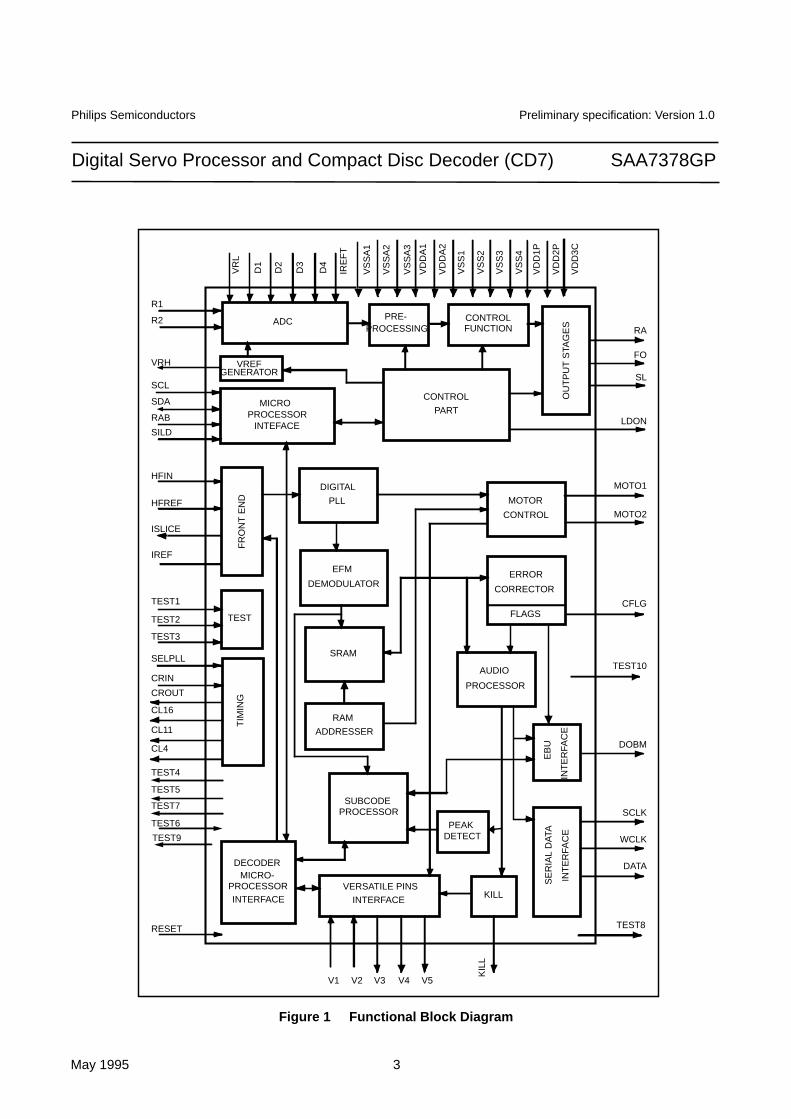
Figure 1 Functional Block Diagram
TEST9

Philips Semiconductors Preliminary specification: Version 1.0
May 1995 4
Digital Servo Processor and Compact Disc Decoder (CD7) SAA7378GP
5. PIN DESCRIPTION
SYMBOL PIN DESCRIPTION
VSSA1 1 analogue supply*
VDDA1 2 analogue supply*
D1 3 unipolar current input (central diode signal input)
D2 4 unipolar current input (central diode signal input)
D3 5 unipolar current input (central diode signal input)
VRL 6 reference input for ADC
D4 7 unipolar current input (central diode signal input)
R1 8 unipolar current input (satellite diode signal input)
R2 9 unipolar current input (satellite diode signal input)
IREFT 10 current reference for calibration ADC
VRH 11 reference output from ADC
VSSA2 12 analogue supply*
SELPLL 13 selects whether internal clock multiplier PLL is used
ISLICE 14 current feedback from data slicer
HFIN 15 comparator signal input
VSSA3 16 analogue supply*
HFREF 17 comparator common mode input
IREF 18 reference current pin (nominally VDD/2)
VDDA2 19 analogue supply*
TEST1 20 test control input; this pin should be tied LOW
CRIN 21 crystal/resonator input
CROUT 22 crystal/resonator output
TEST2 23 test control input; this pin should be tied LOW
CL16 24 16.9344 MHz system clock output
CL11 25 11.2896 MHz or 5.6448MHz clock output (tri-state)
RA 26 radial actuator output
FO 27 focus actuator output
SL 28 sledge control output
TEST3 29 test control input; this pin should be tied LOW
VDD1P 30 digital supply periphery*
DOBM 31 bi-phase mark output (externally buffered) (tri-state)
VSS1 32 digital supply*
MOTO1 33 motor output 1; versatile (tri-state)
MOTO2 34 motor output 2; versatile (tri-state)
TEST4 35 test output pin; this pin should be left unconnected
TEST5 36 test output pin; this pin should be left unconnected

Philips Semiconductors Preliminary specification: Version 1.0
May 1995 5
Digital Servo Processor and Compact Disc Decoder (CD7) SAA7378GP
* Note: All supply pins must be connected to the same external power supply voltage.
TEST6 37 test input; this pin should be tied LOW
TEST7 38 test output pin; this pin should be left unconnected
VSS2 39 digital supply*
V5 40 versatile output pin
V4 41 versatile output pin
V3 42 versatile output pin (open drain)
KILL 43 kill output - programmable (open drain)
TEST8 44 test output pin; this pin should be left unconnected
DATA 45 serial data output (tri-state)
WCLK 46 word clock output (tri-state)
VDD2P 47 digital supply periphery*
SCLK 48 serial bit clock output (tri-state)
VSS3 49 digital supply*
CL4 50 4.2336 MHz µP clock output
SDA 51 µP interface data I/O line (open drain output)
SCL 52 µP interface clock line
RAB 53 µP interface R/W and load control line
SILD 54 µP interface R/W and load control line
N/C 55 No connection
VSS4 56 digital supply*
RESET 57 power-on reset input (active low)
TEST9 58 test output pin; this pin should be left unconnected
VDD3C 59 digital supply core*
TEST10 60 test output pin; this pin should be left unconnected
CFLG 61 correction flag output (open drain)
V1 62 versatile input pin
V2 63 versatile input pin
LDON 64 laser drive on output (open drain)
SYMBOL PIN DESCRIPTION

Philips Semiconductors Preliminary specification: Version 1.0
May 1995 6
Digital Servo Processor and Compact Disc Decoder (CD7) SAA7378GPH
FR
EF
17
IRE
F18
VD
DA
219
TE
ST
120
CR
IN21
CR
OU
T22
TE
ST
223
CL1
624
CL1
125
RA
26
FO
27
SL
28
TE
ST
329
VD
D1 P
30
DO
BM
31
VS
S1
32
64LD
ON
63V
2
62V
1
61C
FLG
60T
ES
T10
59V
DD
3 C
58T
ES
T9
57R
ES
ET
56V
SS4
55N
C
54S
ILD
53R
AB
52S
CL
51S
DA
50C
L4
49V
SS3
VSSA1 1
VDDA1 2
D1 3
D2 4
D3 5
VRL 6
D4 7
R1 8
R2 9
IREFT 10
VRH 11
VSSA2 12
SELPLL 13
ISLICE 14
HFIN 15
VSSA3 16
48 SCLK
47 VDD2P
46 WCLK
45 DATA
44 TEST8
43 KILL
42 V3
41 V4
40 V5
39 VSS2
38 TEST7
37 TEST6
36 TEST5
35 TEST4
34 MOTO2
33 MOTO1
SAA7378
Figure 2 Pinning Diagram

Philips Semiconductors Preliminary specification: Version 1.0
May 1995 7
Digital Servo Processor and Compact Disc Decoder (CD7) SAA7378GP
6. LIMITING VALUESIn accordance with the Absolute Maximum Rating System (IEC 134).
Notes: 1) All VDD and VSS connections must be made externally to the same power supply.
2) Equivalent to discharging a 100pF capacitor via a 1.5kΩ series resistor with a rise time of 15ns.
3) Equivalent to discharging a 200pF capacitor via a 2.5µH series inductor.
SYMBOL PARAMETER CONDITIONS MIN MAX UNIT
VDD supply voltage note 1 -0.5 +6.5 V
VI(max) maximum Input voltage (any input) -0.5 VDD + 0.5 V
VO Output voltage (any output) -0.5 +6.5 V
VDDDIFF Difference between VDDA and VDDD ± 0.25 V
IO Output current (continuous) ± 20 mA
IIK DC input diode current (continuous) ± 20 mA
Tamb operating ambient temperature 5 +70 °CTstg storage temperature -55 +125 °CVes1 electrostatic handling note 2 -2000 +2000 V
Ves2 electrostatic handling note 3 -200 +200 V

Philips Semiconductors Preliminary specification: Version 1.0
May 1995 8
Digital Servo Processor and Compact Disc Decoder (CD7) SAA7378GP
7. FUNCTIONAL DESCRIPTION OF THE DECODER PART
7.1 Principle Operation Modes of the Decoder Part
The decoding part operates at single speed and supports a full audio specification.
A simplified data flow through the decoder part is shown in Figure 5.
7.1.1 Crystal Frequency Selection
The SAA7378 which has an internal phase locked loop clock multiplier, can be used with 33.8688, 16.9344 or 8.4672MHzcrystal frequencies by setting register B and SELPLL as shown below.
The internal clock multiplier, controlled by SELPLL, should only be used if an 8.4672MHz crystal, ceramic resonator orexternal clock is present.
Note: The CL11 output is a 5.6448MHz clock if a 16.9344MHz external clock is used.
7.1.2 Standby Modes
The SAA7378 may be placed in two standby modes, (Note that the device core is still active), selected by register B :
Standby 1 : "CD-STOP" mode. Most I/O functions are switched off.Standby 2: "CD-PAUSE" mode. Audio output features are switched off, but the motor loop, the motor output and the
subcode interfaces remain active. This is also called a "Hot Pause".
In the standby modes the various pins will have following values:
MOTO1, MOTO2: Put in Hi-z, PWM mode (standby 1 and reset : operating in standby 2).Put in Hi-z, PDM mode (standby1 and reset: operating in standby 2).
SCL,SDA, SILD, RAB: No interaction. Normal operation continues.SCLK, WCLK, DATA, CL11, DOBM: Tri-state in both standby modes. Normal operation continues after reset.CRIN, CROUT, CL16, CL4: No interaction. Normal operation continues.V1, V2, V3, V4, V5, CFLG: No interaction. Normal operation continues.
7.2 Crystal Oscillator
The crystal oscillator is a conventional 2 pin design operating at 8 MHz to 35 MHz. This oscillator is capable of working withceramic resonators as well as with both fundamental and third overtone crystals. External components should be used tosuppress the fundamental output of the third overtone crystals as shown below in Figure 3. Typical oscillation frequenciesrequired are 8.4672MHz, 16.9344MHz or 33.8688MHz depending on the internal clock settings used and whether or not theclock multiplier is enabled.
Register B SELPLL crystal frequency (MHz)
00xx 0 33.8688
00xx 1 8.4672
01xx 0 16.9344

Philips Semiconductors Preliminary specification: Version 1.0
May 1995 9
Digital Servo Processor and Compact Disc Decoder (CD7) SAA7378GP
3.3µH
Figure 3 Crystal Oscillator Circuits
CRIN8.4672MHz
Oscillator
SAA7378
8.4672MHz Fundamental Configuration
33.8688MHz 3rd Overtone Configuration
CROUT
1nF
22pF22pF
330Ω
CRIN33.8688MHz
Oscillator
100kΩ
SAA7378
CROUT
10pF10pF
330Ω
100kΩ

Philips Semiconductors Preliminary specification: Version 1.0
May 1995 10
Digital Servo Processor and Compact Disc Decoder (CD7) SAA7378GP
7.3 Data Slicer and Clock Regenerator
The SAA7378 has an integrated slice level comparator which can be clocked by the crystal frequency clock, or 8 times thecrystal frequency clock (if SELPLL is set high while using an 8.4672MHz crystal, and register 4 is set to 0xxx ). The slice levelis controlled by an internal current source applied to an external capacitor under the control of the Digital Phase-Locked Loop(DPLL).
Regeneration of the bit clock is achieved with an internal fully digital PLL. No external components are required and the bitclock is not output. The PLL has two registers (8 and 9) for selecting bandwidth and equalization.
For certain applications an offtrack input is necessary. This is internally connected from the servo part (its polarity can bechanged by the foc_parm1 parameter), but may be input via the V1 pin if selected by register C. If this flag is high, theSAA7378 will assume that its servo part is following on the wrong track, and will flag all incoming HF data as incorrect.
7.4 Demodulator
7.4.1 Frame Sync Protection
A double timing system is used to protect the demodulator from erroneous sync patterns in the serial data. The mastercounter is only reset if:
- a sync coincidence detected; sync pattern occurs 588 ± 1 EFM clocks after the previous sync pattern.- a new sync pattern is detected within ± 6 EFM clocks of its expected position.
The sync coincidence signal is also used to generate the PLL lock signal, which is active high after 1 sync coincidence found,and reset low if during 61 consecutive frames no sync coincidence is found. The PLL lock signal can be accessed via theSDA or STATUS pins selected by register 2 and 7.
Also incorporated in the demodulator is a RL2 (Run Length 2) correction circuit. Every symbol detected as RL2 will bepushed back to RL3. To do this the phase error of both edges of the RL2 symbol are compared and the correction is executedat the side with the highest error probability.
7.4.2 EFM Demodulation
The 14-bit EFM data and subcode words are decoded into 8-bit symbols.
+
-D Q
DPLL
crystalclock
HFIN
HFREF
IREF
ISLICE
VSS
VDD
HF
input
2.2nF2.2kΩ
22kΩ
47pF
22nF
VSSA
VSSA
VDD/2
100nF
100 µA
100 µA
Figure 4 Data Slicer Showing Typical Application Components

Philips Semiconductors Preliminary specification: Version 1.0
May 1995 11
Digital Servo Processor and Compact Disc Decoder (CD7) SAA7378GP
Fig
ure
5
SA
A73
78 D
ecod
er F
unct
ion:
Sim
plifi
ed D
ata
Flo
w
KIL
L
SU
BC
OD
EP
RO
CE
SS
OR
ER
RO
RC
OR
RE
CT
OR
FIF
O
FA
DE
/MU
TE
/IN
TE
RP
OLA
TE
DIG
ITA
LF
ILT
ER
KIL
L
PH
AS
EC
OM
PE
NS
AT
ION
DE
EM
PH
AS
ISF
ILT
ER
IIS INT
ER
FA
CE
EB
UIN
TE
RF
AC
E
µP INT
ER
FA
CE
DIG
ITA
L P
LL &
DE
MO
DU
LAT
OR
1 0
1 : n
o pr
eem
phas
is d
etec
ted
V3
SC
LKW
CLK
DA
TA
reg
3 r
eg 3
reg
C
SD
A
DO
BM
reg
A
outp
ut fr
omda
ta s
licer
AN
D r
eg D
≠ 0
1xx
0 : p
reem
phas
is d
etec
ted
OR
reg
D =
01x
x (d
eem
phas
is s
igna
l at V
5)

Philips Semiconductors Preliminary specification: Version 1.0
May 1995 12
Digital Servo Processor and Compact Disc Decoder (CD7) SAA7378GP
7.5 Subcode Data Processing
7.5.1 Q-Channel ProcessingThe 96-bit Q-channel word is accumulated in an internal buffer. The last 16 bits are used internally to perform a CyclicRedundancy Check (CRC). If the data is good, the SUBQREADY-I signal will go low. SUBQREADY-I can be read via theSDA or STATUS pins, selected via register 2. Good Q-channel data may be read from SDA.
7.5.2 Subcode Channels Q-WData of subcode channels, Q-W, is available in the EBU output (DOBM).
7.6 FIFO and Error Corrector
The SAA7378 has a ±8 frame FIFO. The error corrector is a t = 2, e = 4 type, with error corrections on both C1 (32 symbol)and C2 (28 symbol) frames. Four symbols are used from each frame as parity symbols. This error corrector can correct upto two errors on the C1 level and up to four errors on the C2 level.The error corrector also contains a flag processor. Flags are assigned to symbols when the error corrector cannot ascertainif the symbols are definitely good. C1 generates output flags which are read after (de-interleaving) by C2, to help in thegeneration of C2 output flags.The C2 output flags are used by the interpolator for concealment of uncorrectable errors. They are also output via the EBUsignal (DOBM).
7.6.1 Flags Output (CFLG)
The flags output pin CFLG (open-drain) shows the status of the error corrector and interpolator and is updated every frame7.35kHz. In the SAA7378 chip a 1-bit flag is present on the CFLG pin as shown in Figure 6.This signal shows the status ofthe error corrector and interpolator.
F1 F2 F3 F4 F5 F6 F7 F1
11.3µs
33.9µs
F8 F8
33.9 µs
Figure 6 Flag Output Timing Diagram

Philips Semiconductors Preliminary specification: Version 1.0
May 1995 13
Digital Servo Processor and Compact Disc Decoder (CD7) SAA7378GP
The first flag bit, F1, is the absolute time sync signal; the FIFO-passed subcode-sync and relates the position of the subcode-sync to the audio data (DAC output). The output flags can be made available at bit 4 of the EBU data format (LSB of the 24-bit data word), if selected by register A.
7.7 Audio Functions
7.7.1 Deemphasis and Phase Linearity
When pre-emphasis is detected in the Q-channel subcode, the digital filter automatically includes a deemphasis filter section.When deemphasis is not required, a phase compensation filter section controls the phase of the digital oversampling filterto ≤ ±1° within the band 0 - 16 kHz. With deemphasis the filter is not phase linear.If the deemphasis signal is set to be available at V5, selected via register D, then the deemphasis filter is bypassed.
7.7.2 Digital Oversampling Filter
The SAA7378 contains a 2 - 4 times oversampling IIR filter. The filter specification of the 4 x oversampling filter is given inthe table below.
These attenuations do not include the sample and hold at the external DAC output or the DAC post filter. When using theoversampling filter, the output level is scaled -0.5 dB down, to avoid overflow on full scale sine wave inputs (0 - 20 kHz).
F1 F2 F3 F4 F5 F6 F7 F8 MEANING
0 x x x x x x x No Absolute Time sync
1 x x x x x x x Absolute Time sync
x 0 0 x x x x x C1 frame contained no errors
x 0 1 x x x x x C1 frame contained 1 error
x 1 0 x x x x x C1 frame contained 2 errors
x 1 1 x x x x x C1 frame uncorrectable
x x x 0 0 x x 0 C2 frame contained no errors
x x x 0 0 x x 1 C2 frame contained 1 error
x x x 0 1 x x 0 C2 frame contained 2 errors
x x x 0 1 x x 1 C2 frame contained 3 error
x x x 1 0 x x 0 C2 frame contained 4 errors
x x x 1 1 x x 1 C2 frame uncorrectable
x x x x x 0 0 x No interpolations
x x x x x 0 1 x At least one 1-sample interpolation
x x x x x 1 0 x At least one hold and no interpolations
x x x x x 1 1 x At least one hold and one 1-sample interpolation
PASSBAND ATTENUATION
0 - 19 kHz ≤0.001 dB
19 - 20 kHz ≤0.03 dB
STOPBAND ATTENUATION
24.0 kHz ≥25 dB
24 - 27 kHz ≥38 dB
27 - 35 kHz ≥40 dB
35 - 64 kHz ≥50 dB
64 - 68 kHz ≥31 dB
68 kHz ≥35 dB
69 - 88 kHz ≥40 dB

Philips Semiconductors Preliminary specification: Version 1.0
May 1995 14
Digital Servo Processor and Compact Disc Decoder (CD7) SAA7378GP
7.7.3 ConcealmentA 1-sample linear interpolator becomes active if a single sample is flagged as erroneous but cannot be corrected. Theerroneous sample is replaced by a level midway between the preceding and following samples. Left and right channels haveindependent interpolators. If more than one consecutive non-correctable sample is found, the last good sample is held. A 1-sample linear interpolation is then performed before the next good sample (Figure 7). .
7.7.4 Mute, Full Scale, Attenuation and Fade
A digital level controller is present on the SAA7378 which performs the functions of soft mute, full scale, attenuation andfade; these are selected via register 0.
Mute: signal reduced to 0 in a maximum of 128 steps; 3ms.Attenuate: signal scaled by -12dB.Full scale: ramp signal back to 0dB level. From mute takes 3ms.Fade: activates a 128 stage counter which allows the signal to be scaled up/down by 0.07dB steps.
128 = full scale120 = -0.5dB (ie. full scale if oversampling filter used)32 = -12dB0 = mute
7.7.5 Peak Detector
The peak detector measures the highest audio level (absolute value) on positive peaks for left and right channels. The 8most significant bits are output in the Q-channel data in place of the CRC bits. Bits 81 to 88 contain the left peak value (bit88 = MSB) and bits 89 to 96 contain the right peak value (bit 96 = MSB). The values are reset after reading Q-channel datavia SDA.
Interpolation InterpolationHold
OK Error OK OK OKError Error Error
Figure 7 Concealment Mechanism

Philips Semiconductors Preliminary specification: Version 1.0
May 1995 15
Digital Servo Processor and Compact Disc Decoder (CD7) SAA7378GP
7.8 DAC Interface
The SAA7378 is compatible with a wide range of Digital-Analogue Converters. Six formats are supported and are shownbelow. Figure 8 and Figure 9 show the Philips IIS and the EIAJ data formats respectively. All formats are MSB first and fs is44.1kHz. The polarity of the WCLK and the data can be inverted; selectable by register 7.
REGISTER 3SAMPLE
FREQUENCYNo ofBITS
SCLKMHz
FORMAT INTERPOLATION
0000 4fs 16 8.4672 * n EIAJ - 16 bits yes
0100 4fs 18 8.4672 * n EIAJ - 18 bits yes
1100 4fs 18 8.4672 * n Philips I2S - 18 bits yes
0011 2fs 16 4.2336 * n EIAJ - 16 bits yes
0111 2fs 18 4.2336 * n EIAJ - 18 bits yes
1111 2fs 18 4.2336 * n Philips I2S - 18 bits yes
17 0 15
SCLK
DATA
WCLKLEFT CHANNEL DATA (WCLK NORMAL POLARITY)
Figure 8 Philips I 2S Data Format (18-Bit Word Length Shown )
116 141 0
170 0 17
SCLK
DATA
WCLKLEFT CHANNEL DATA
Figure 9 EIAJ Data Format (18-Bit Word Length Shown)

Philips Semiconductors Preliminary specification: Version 1.0
May 1995 16
Digital Servo Processor and Compact Disc Decoder (CD7) SAA7378GP
7.9 EBU Interface
The biphasemark digital output signal at pin DOBM is according to the format defined by the IEC958 specification. TheDOBM pin can be held low; selected via register A:
7.9.1 Format
The digital audio output consists of 32-bit words ("subframes") transmitted in biphasemark code (two transitions for a logic’1’and one transition for a logic’0’). Words are transmitted in blocks of 384.
Sync: The Sync word is formed by violation of the biphase rule and therefore does not contain any data. Itslength is equivalent to 4 data bits. The 3 different sync patterns indicate the following situations:
Sync B:- Start of a block (384 words), word contains left sample.Sync M:- Word contains left sample (no block start).Sync W:- Word contains right sample.
Audio sample: Left and right samples are transmitted alternately.Validity flag: Audio samples are flagged (bit 28 = ’1’) if an error has been detected but was uncorrectable. This flag
remains the same even if data is taken after concealmentUser data: Subcode bits Q until W from the subcode section are transmitted via the user data bit. This data is
asynchronous with the block rate.Channel status: The channel status bit is the same for left and right words. Therefore a block of 384 words contains 192
channel status bits. The category code is always CD. The bit assignment is shown below.
7.10 KILL Circuit
The KILL circuit detects digital silence by testing for an all-zero or all-ones data word in the left or right channel before thedigital filter. The output is switched active-low when silence has been detected for at least 250ms, or if Mute is active. Twomodes are available, selected by register C:
- 1 pin kill: KILL active low indicates silence detected on both left and right channels.- 2 pin kill: KILL active low indicates silence detected on left channel.
V3 active low indicates silence detected on right channel.
sync bits 0 - 3
auxiliary bits 4 - 7 Not used. Normally zero
error flags bit 4 CFLG error and interpolation flags when selected by register A
audio sample bits 8 - 27 First 4 bits not used (always zero). 2’s compliment. LSB = bit 12, MSB = bit 27
validity flag bit 28 Valid = logic 0
user data bit 29 Used for subcode data (Q to W)
channel status bit 30 Control bits and category code
parity bit bit 31 Even parity for bits 4 to 30
control bits 0 - 3 copy of CRC checked Q-channel control bits 0 - 3; bit 2 is logic 1 when copy permitted; bit 3 is logic 1 when recording has preemphasis
reserved mode bits 4 - 7 always zero.
category code bits 8 - 15 CD: bit 8 = logic1, all other bits = logic 0
clock accuracy bits 28 - 29 set by register A: 10 = level I 00 = level II 01 = level III
remaining bits 16 - 27bits 30 - 191
always zero

Philips Semiconductors Preliminary specification: Version 1.0
May 1995 17
Digital Servo Processor and Compact Disc Decoder (CD7) SAA7378GP
7.11 The VIA Interface
The SAA7378 has five pins that can be reconfigured for different applications:
7.12 Spindle Motor Control
7.12.1 Motor Output ModesThe spindle motor speed is controlled by a fully integrated digital servo. Address information from the internal ± 8 frameFIFO and Disc speed information are used to calculate the motor control output signals. Several output modes, selected byregister 6, are supported:
- Pulse Density, 2-line (true complement output), 1MHz sample frequency.- PWM-output, 2-line, 22.05kHz modulation frequency.- PWM-output, 4-line, 22.05kHz modulation frequency.- CDV motor mode.
7.12.1.1 Pulse Density Output Mode
In the Pulse Density mode the motor output pin, MOTO1, is the pulse density modulated motor output signal. 50% duty cyclecorresponds with the motor not actuated, higher duty cycles mean acceleration, lower mean braking. In this mode, theMOTO2 signal is the inverse of the MOTO1 signal. Both signals change state only on the edges of a 1MHz internal clocksignal. Possible application diagrams are shown in Figure 10.
7.12.1.2 PWM Output Mode, 2-LineIn the PWM mode the motor acceleration signal is put in pulse-width modulation form on the MOTO1 output, and the motorbraking signal is pulse-width modulated on the MOTO2 output. Figure 11 shows the timing and Figure 12 a typical applicationdiagram.
PIN NAME PIN no. TYPE CONTROLREGISTERADDRESS
CONTROLREGISTER
DATA
FUNCTION
V1 62 Input 1100 xxx1 External offtrack signal input
xxx0 Internal offtrack signal usedInput may be read via decoder status bit;selected via register 2.
V2 63 Input Input may be read via decoder status bit;selected via register 2.
V3 42 Output 1100 xx0x Kill output for Right channel
x01x Output = 0
x11x Output = 1
V4 41 Output 1101 0000 4-line motor drive (using V4 & V5)
xx10 Output = 0
xx11 Output = 1
V5 40 Output 1101 01xx Deemphasis output (active high)
10xx Output = 0
11xx Output = 1

Philips Semiconductors Preliminary specification: Version 1.0
May 1995 18
Digital Servo Processor and Compact Disc Decoder (CD7) SAA7378GP
7.12.1.3 PWM Output Mode, 4-Line
Using two extra outputs from the Versatile Pins Interface, it is possible to use the SAA7378 with a 4-input motor bridge.
+-
M+-
MOTO1 MOTO222 k 22 k
10n10n
VSS VSS
+-
VSS
MOTO122 k
10 n
VSS
22 k
22 kVDD
M
Figure 10 Motor Pulse Density Application Diagrams
VSS
VDD
22 k
22 k
Accelerate Brake
trep = 45 µstdead = > 240 ns
MOTO1
MOTO2
Figure 11 2-Line PWM Mode Timing
MOTO1 MOTO2
VSS
+
M
Figure 12 Motor 2-Line PWM Mode Application Diagram
10 100n

Philips Semiconductors Preliminary specification: Version 1.0
May 1995 19
Digital Servo Processor and Compact Disc Decoder (CD7) SAA7378GP
Figure 13 shows the timing, and Figure 14 a typical application diagram.
7.12.1.4 CDV/CAV Output Mode
In the CDV motor mode, the FIFO position will be put in pulse-width modulated form on the MOTO1 pin (carrier frequency300Hz), and the PLL frequency signal will be put in pulse-density modulated form (carrier frequency 4.23MHz) on theMOTO2 pin. The integrated motor servo is disabled in this mode.
Notes: 1) The PWM signal on MOTO1 corresponds to a total memory space of 20 frames, therefore the nominal FIFOposition (half full) will result in a PWM output of 60%.
7.12.2 Spindle Motor Operating Modes
The motor servo has the following operation modes controlled by register 1:Start mode 1 Disc is accelerated by applying a positive voltage to the spindle motor. No decisions are involved and the
PLL is reset. No Disc speed information is available for the µP.Start mode 2 The Disc is accelerated as in Start mode 1, however the PLL will monitor the Disc speed. When the Disc
reaches 75% of its nominal speed, the controller will switch to Jump mode. The motor status signalsselectable via register 2 are valid.
Jump mode Motor servo enabled but FIFO kept reset at 50%, integrator is held. The audio is muted but it is possibleto read the subcode.
Jump mode 1 Similar to Jump mode but motor integrator is kept at zero. Used for long jumps, where there is a largechange in disc speed.
Accelerate Brake
trep = 45 µstdead = > 240 ns
MOTO1
MOTO2
tovl = 240 ns
V4
V5
Figure 13 4-Line PWM Mode Timing
MOTO1 MOTO2
V4 V5
+
M
Figure 14 Motor 4-Line PWM Mode Application Diagram
10 100n
VSS

Philips Semiconductors Preliminary specification: Version 1.0
May 1995 20
Digital Servo Processor and Compact Disc Decoder (CD7) SAA7378GP
Play mode FIFO released after resetting to 50%. Audio mute released.Stop mode 1 Disc is braked by applying a negative voltage to the motor. No decisions are involved.Stop mode 2 The Disc is braked as in Stop mode 1, but the PLL will monitor the Disc speed. As soon as the Disc
reaches 12% (or 6%, depending on the programmed brake percentage, via register E) of its nominalspeed, the MOTSTOP status signal will go high and switch the motor servo to Off mode.
Off mode Motor not steered.In the SAA7378 decoder there is an anti-wind-up mode for the motor servo, selected via register 1. When the anti-wind-upmode is activated the motor servo integrator will hold if the motor output saturates.
7.12.2.1 Power Limit
In Start mode 1, Start mode 2, Stop mode 1 and Stop mode 2, a fixed positive or negative voltage is applied to the motor.This voltage can be programmed as a percentage of the maximum possible voltage, via register 6, to limit current drainduring start and stop. The following power limits are possible:
100% (no power limit), 75%, 50%, or 37% of maximum.
7.12.3 Loop Characteristics
The gain and crossover frequencies of the motor control loop can be programmed via registers 4 and 5. The followingparameter values are possible:
Gains: 3.2, 4.0, 6.4, 8.0, 12.8, 16, 25.6, 32Crossover frequency f4: 0.5Hz, 0.7Hz, 1.4Hz, 2.8HzCrossover frequency f3: 0.85Hz, 1.71Hz, 3.42Hz
7.12.4 FIFO Overflow
If FIFO overflow occurs during Play mode (eg: as a result of motor rotational shock), the FIFO will be automatically reset to50% and the audio interpolator tries to conceal as much as possible to minimise the effect of data loss.
A
fBWf4 f3
Figure 15 Motor Servo Bode Diagram

Philips Semiconductors Preliminary specification: Version 1.0
May 1995 21
Digital Servo Processor and Compact Disc Decoder (CD7) SAA7378GP
8. FUNCTIONAL DESCRIPTION OF THE SERVO PART
8.1 Diode Signal ProcessingThe photo detector in conventional two-stage three-beam compact disc systems normally contains six discrete diodes. Fourof these diodes (three for single focault systems) carry the central aperture (CA) signal while the other two diodes (satellitediodes) carry the radial tracking information. The CA signal is processed into an HF signal (for the decoder function) and LFsignal (information for the focus servo loop) before it is supplied to the SAA7378.
The analog signals from the central and satellite diodes are converted into a digital representation using analog to digitalconverters (ADCs). The ADCs are designed to convert unipolar currents into a digital code. The dynamic range of the inputcurrents is adjustable within a given range which is dependent on the value of external resistor connected to IREFT. Themaximum current for the central diodes and satellite diodes is given below:
Iin(max, central) = (2.4 * 106 / RIREFT) µAIin(max, satellite) = (1.2 * 106 / RIREFT) µA
The VRH voltage is internally generated by control circuitry which takes care that the VRH voltage is adjusted depending uponthe spread of internal capacitors, using the reference current generated by the external resistor on IREFT. In the applicationVRL is connected to VSSA1. The maximum input currents for a range of resistors is given below:
This mode of VRH automatic adjustment can be selected by the preset latch command.
Alternatively the dynamic range of the input currents can be made dependent on the ADC reference voltages; VRL and VRH,for this case the maximum current for the central diodes and satellite diodes is given below:
Iin(max, central) = fsys * (VRH - VRL) * 1.0 * 10-6 µAIin(max, satellite) = fsys * (VRH - VRL) * 0.5 * 10-6 µA where fsys = 4.2336MHz
VRH is generated internally, and there are 32 levels which can be selected under software control, via the preset latchcommand. With this command the VRH voltage can be set to 2.5V then modified, decremented one level or incremented, byresending the command the required number of times. In the application VRL is connected to VSSA1.
8.2 Signal ConditioningThe digital codes retrieved from the ADCs are applied to logic circuitry to obtain the various control signals. The signals fromthe central aperture diodes are processed to obtain a normalised focus error signal:
RIREFT(Ω)
diode input current range
D1,D2,D3,D4(µA)
R1,R2(µA)
220k 10.909 5.455
240k 10.000 5.000
270k 8.889 4.444
300k 8.000 4.000
330k 7.273 3.636
360k 6.667 3.333
390k 6.154 3.077
430k 5.581 2.791
470k 5.106 2.553
510k 4.706 2.353
560k 4.286 2.143
620k 3.871 1.935
D1 - D2FEn = D3 - D4
-D1 + D2 D3 + D4

Philips Semiconductors Preliminary specification: Version 1.0
May 1995 22
Digital Servo Processor and Compact Disc Decoder (CD7) SAA7378GP
where the detector set up is assumed as shown in Figure 16.
In the case of single Foucault focusing method, the signal conditioning can be switched under software control such that thesignal processing is as follows:
The error signal, FEn, is further processed by a proportional integral and differential (PID) filter section.A focus OK (FOK) flag is generated by means of the central aperture signal and an adjustable reference level. This signalis used to provide extra protection for the track-loss (TL) generation, the focus start up procedure and the drop out detection.The radial or tracking error signal is generated by the satellite detector signals R1 and R2. The radial error signal can beformulated as follows:
where the index ’s’ indicates the automatic scaling operation which is performed on the radial error signal. This scaling isnecessary to avoid non-optimal dynamic range usage in the digital representation and reduces the radial bandwidth spread.Furthermore, the radial error signal will be made free from offset during start up of the disc.The four signals from the central aperture detectors together with the satellite detector signals generate a track positionsignal (TPI), which can be formulated as follows:
Where the weighting factor sum_gain is generated internally, by the SAA7378, during initialisation.
8.3 Focus Servo SystemThe SAA7378 includes the following focus servo functions:
8.3.1 Focus Start-upFive initially loaded coefficients influence the start-up behaviour of the focus controller. The automatically generated trianglevoltage can be influenced by 3 parameters; for height (ramp_height) and DC-offset (ramp_offset) of the triangle and itssteepness (ramp_incr).
For protection against false focus point detections two parameters are available, which are an absolute level on the CA-signal (CA_start) and a level on the FEn signal (FE_start). When this CA level is reached the FOK signal becomes true.
If this FOK signal is true and the level on the FEn signal is reached, the focus PID is enabled to switch on when the next zerocrossing is detected in the FEn signal.
Figure 16 Detector Arrangement
Satellitediode R1
D2D3
D1
single Foucault
Satellitediode R2
Satellitediode R1
D3
D2
D4
D1
Satellitediode R2
Satellitediode R1
D3D2
D4
D1
Satellitediode R2
astigmatic focus double Foucault
FEn = 2 D1 - D2*
D1 + D2
REs = (R1 - R2) * re_gain + (R1 - R2) re_offset*
TPI = sign [ (D1 + D2 + D3 + D4) - (R1 + R2) sum_gain ]*

Philips Semiconductors Preliminary specification: Version 1.0
May 1995 23
Digital Servo Processor and Compact Disc Decoder (CD7) SAA7378GP
8.3.2 Focus Position Control LoopThe focus control loop contains a digital PID controller which has 5 parameters available to the user. These coefficientsinfluence the integrating (foc_int), proportional (foc_lead_length, part of foc_parm3) and differentiating (foc_pole_lead, partof foc_parm1) action of the PID and a digital low pass filter (foc_pole_noise, part of foc_parm2) following the PID. The fifthcoefficient foc_gain influences the loop gain.
8.3.3 Drop-out DetectionThis detector can be influenced by one parameter (CA_drop). The FOK signal will become false and the integrator of thePID will hold if the CA signal drops below this programmable absolute CA level. When the FOK signal becomes false it isassumed, initially, to be caused by a black dot.
8.3.4 Focus Loss Detection and Fast RestartWhenever FOK is false for longer than about 3ms, it is assumed that the focus point is lost. A fast restart procedure is initiatedwhich is capable of restarting the focus loop within 200 to 300ms depending on the microprocessor programmed coefficients.
8.3.5 Focus Loop Gain SwitchingThe gain of the focus control loop (foc_gain) can be multiplied by a factor of 2 or divided by a factor of 2 during normaloperation. The integrator value of the PID is corrected accordingly. The differentiating (foc_pole_lead) action of the PID canbe switched at the same time as the gain switching is performed.
8.4 Radial Servo SystemThe SAA7378 includes the following focus servo functions:
8.4.1 Level InitialisationDuring start-up an automatic adjustment procedure is activated to set the values of the radial error gain (re_gain), offset(re_offset) and satellite sum gain (sum_gain) for TPI level generation. The initialisation procedure runs in a radial open loopsituation and is ≤300ms. This start-up time period may coincide with the last part of the motor start up time period.
Automatic gain adjustment: As a result of this initialisation the amplitude of the RE signal is adjusted within ±10%around the nominal RE amplitude
Offset adjustment: The additional offset in RE due to the limited accuracy of the start-up procedure is lessthan ±50nm.
TPI level generation: The accuracy of the initialisation procedure is such that the duty cycle range of TPIbecomes 0.4 < dutycycle < 0.6 (def. dutycycle: TPI-’high’ / TPI-period).
8.4.2 Sledge ControlThe microprocessor can move the sledge in both directions via the steer sledge command.
8.4.3 Tracking ControlThe actuator is controlled using a PID loop filter with user defined coefficients and gain. For stable operation between thetracks, the S-curve is extended over 0.75 track. Upon request from the microprocessor S-curve extension over 2.25 tracksis used, automatically changing to access control when exceeding those 2.25 tracks.
Both modes of S-curve extension make use of a track-count mechanism. In this mode track counting results in an ’automaticreturn to zero track’, to avoid major music rhythm disturbances in the audio output for improved shock resistance. The sledgeis continuously controlled using the filtered value of the radial PID output. Alternatively the microprocessor can read theaverage voltage on the radial actuator, and provides the sledge with step pulses to reduce power consumption. Filtercoefficients of the continuous sledge control are user presettable.

Philips Semiconductors Preliminary specification: Version 1.0
May 1995 24
Digital Servo Processor and Compact Disc Decoder (CD7) SAA7378GP
8.4.4 AccessThe access procedure is divided into two different modes, depending upon the requested jump size.
The access procedure makes use of a track counting mechanism, a velocity signal based on a fixed number of tracks passedwithin a fixed time interval, a velocity setpoint calculated from the number of tracks to go and a user programmable parameterindicating the maximum sledge performance.If the number of tracks to go is greater than brake_distance then the sledge jump mode should be activated else the actuatorjump should be performed. The requested jump size together with the required sledge breaking distance at maximum accessspeed defines the value brake_distance.During the actuator jump mode, velocity control with a PI controller is used for the actuator. The sledge is then continuouslycontrolled using the filtered value of the radial PID output. All filter parameters (for actuator and sledge) are userprogrammable.In sledge jump mode maximum power (user programmable) is applied to the sledge in the correct direction, while theactuator becomes idle (the contents of the actuator integrator leaks to zero just after the sledge jump mode is initiated).
8.5 Off Track CountingThe track position (TPI) signal is a flag which is used to indicate whether the radial spot is positioned on the track, with amargin of ± 1/4 of the track-pitch. In combination with the radial polarity flag (RP) the relative spot position over the trackscan be determined. These signals are, however afflicted with some uncertainties caused by:
• disc defects such as scratches and fingerprints.• the HF information on the disc, which is considered as noise by the detector signals.
In order to determine the spot position with sufficient accuracy, extra conditions are necessary to generate a track loss (TL)signal as well as an off-track counter value. These extra conditions influence the maximum speed and this implies that,internally, one of the three following counting states is selected:
1. Protected state: used in normal play situations.A good protection against false detection caused by disc defects is important in this state.
2. Slow counting state: used in low velocity track jump situations.In this state a fast response is important rather than the protection against disc defects (if the phaserelationship between TL and RP of 1/2 π radians is affected too much, the direction cannot be determinedaccurately anymore).
3. Fast counting state: used in high velocity track jump situations.Highest obtainable velocity is the most important feature in this state.
8.6 Defect DetectionA defect detection circuit is incorporated into the SAA7378. If a defect is detected, the radial and focus error signals may bezeroed, resulting in better playability. The defect detector can be switched off, applied only to focus control, or applied to bothfocus and radial controls under software control (part of foc_parm1).The defect detector (Figure 17) has programmable setpoints selectable by the parameter, defect_parm.
ACCESS TYPE JUMP SIZE ACCESS SPEED
Actuator jump 1 - brake_distance1 decreasing velocity
Sledge jump brake_distance1 - 32768 maximum power to sledge 1
1 : microprocessor presettable
Figure 17 Defect Detector Block Diagram
Sat1 +
-
FastDecimation Defect Programmablehold-off
Sat2
Slow DefectOutfilter filter filter generation
+

Philips Semiconductors Preliminary specification: Version 1.0
May 1995 25
Digital Servo Processor and Compact Disc Decoder (CD7) SAA7378GP
8.7 Off Track DetectionDuring active radial tracking, off track detection has been realised by continuously monitoring the off track counter value.The off track flag becomes valid whenever the off track counter value is unequal to zero. Depending on the type of extendedS-curve the off track counter is reset after 0.75 extend or at the original track in the 2.25 track extend mode.
8.8 Driver InterfaceThe control signals (pins RA, FO and SL) for the mechanism actuators are pulse density modulated. The modulatingfrequency can be set to either 1.0584MHz (DSD mode) or 2.1168MHz; controlled via the xtra_preset parameter. An analogrepresentation of the output signals can be achieved by connecting a first order low pass filter to the outputs.During reset (ie. RESET pin is held low) the RA, FO and SL pins are high impedance.
8.9 Laser InterfaceThe LDON pin (open drain output) is used to switch the laser off and on; when the laser is on the output is high impedance.The action of the LDON pin is controlled by the xtra_preset parameter; the pin is automatically driven if the focus control loopis active.
8.10 Radial Shock DetectorThe shock detector (block diagram shown in Figure 18) can be switched on during normal track following; and detects withinan adjustable frequency whether disturbances in the radial spot position relative to the track exceed an adjustable level(controlled by shock_level). Every time the radial tracking error (RE) exceeds this level the radial control bandwidth isswitched to twice its original bandwidth and the loop gain is increased by a factor of 4.
The shock detection level is adjustable in 16 steps from 0 to 100% of the traverse radial amplitude which is sent to anamplitude detection unit via an adjustable bandpass filter (controlled by sledge_parm1); lower corner frequency can be setat either 0 or 20Hz, and upper corner frequency at 750 or 1850Hz. The shock detector is switched off automatically duringjump mode.
Figure 18 Block Diagram of Shock Detector
RE High pass filter Amplitude Shock(0 or 20Hz)
Low pass filter(750 or 1850Hz) detection out

Philips Semiconductors Preliminary specification: Version 1.0
May 1995 26
Digital Servo Processor and Compact Disc Decoder (CD7) SAA7378GP
9. MICROPROCESSOR INTERFACECommunication on the microprocessor interface is via a 4-wire bus: the protocol being compatible with SAA7345 (CD6) andTDA1301 (DSIC2):
SCL - serial bit clock.SDA - serial data.RAB - R/W control and data strobe (active high) for writing to registers 0 - F, reading status bit selected via
register 2 and reading Q channel subcode.SILD - R/W control and data strobe (active low) for servo commands.
9.1 Writing Data to Registers 0 - E
The sixteen 4-bit programmable configuration registers, 0 to E (Table 1), can be written to via the microprocessor interfaceusing the protocol shown in Figure 19.
Note that: - SILD must be held high.- A(3:0) identifies the register number, D(3:0) is the data.- the data is latched into the register on the low-high transition of RAB.
9.1.1 Writing Repeated Data to Registers 0 - E
The same data can be repeated several times (eg: for a fade function) by applying extra RAB pulses as shown in Figure 20.Note that SCL must stay high between RAB pulses.
9.2 Reading Decoder Status Information on SDAThere are several internal status signals, selected via register 2, which can be made available on the SDA line. These are:
- SUBQREADY-I Low if new subcode word is ready in Q-channel register.- MOTSTART1 High if motor is turning at 75% or more of nominal speed.- MOTSTART2 High if motor is turning at 50% or more of nominal speed.- MOTSTOP High if motor is turning at 12% or less of nominal speed. Can be set to indicate 6% or less
(instead of 12% or less) via register E.- PLL Lock High if Sync coincidence signals are found.- V1 Follows input on V1 pin.
RAB (µP)
SCL (µP)
SDA (µP)
SDA (SAA7378)Hi-impedance
A3 A2 A1 A0 D3 D2 D1 D0
Figure 19 Microprocessor Write Protocol for Registers 0 to E
RAB (µP)
SCL (µP)
SDA (µP)
SDA (decoder)Hi-impedance
A3 A2 A1 A0 D3 D2 D1 D0
Figure 20 Microprocessor Write Protocol for Registers 0 to E - Repeat Mode
Philips Semiconductors Preliminary specification: Version 1.0
May 1995 27
Digital Servo Processor and Compact Disc Decoder (CD7) SAA7378GP
- V2 Follows input on V2 pin.- MOTOR-OV High if the motor servo output stage saturates.- FIFO-OV High if FIFO overflows.- SHOCK MOTSTART2 + PLL Lock + MOTOR-OV + FIFO-OV + OTD (high if shock detected)- LA-SHOCK Latched SHOCK signal
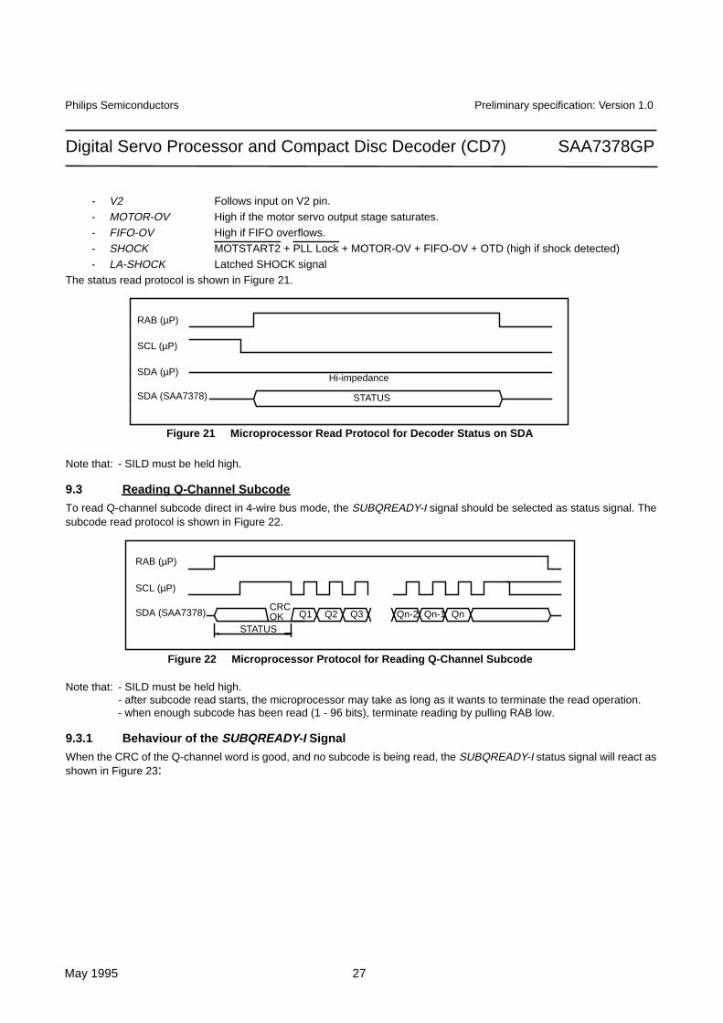
The status read protocol is shown in Figure 21.
Note that: - SILD must be held high.
9.3 Reading Q-Channel Subcode
To read Q-channel subcode direct in 4-wire bus mode, the SUBQREADY-I signal should be selected as status signal. Thesubcode read protocol is shown in Figure 22.
Note that: - SILD must be held high.- after subcode read starts, the microprocessor may take as long as it wants to terminate the read operation.- when enough subcode has been read (1 - 96 bits), terminate reading by pulling RAB low.
9.3.1 Behaviour of the SUBQREADY-I Signal
When the CRC of the Q-channel word is good, and no subcode is being read, the SUBQREADY-I status signal will react asshown in Figure 23:
RAB (µP)
SCL (µP)
SDA (µP)
SDA (SAA7378)
Hi-impedance
STATUS
Figure 21 Microprocessor Read Protocol for Decoder Status on SDA
RAB (µP)
SCL (µP)
SDA (SAA7378) Q1 Q2 Q3 Qn-2 Qn-1 QnCRCOK
STATUS
Figure 22 Microprocessor Protocol for Reading Q-Channel Subcode

Philips Semiconductors Preliminary specification: Version 1.0
May 1995 28
Digital Servo Processor and Compact Disc Decoder (CD7) SAA7378GP
When the CRC is good and subcode is being read, the timing in Figure 24 applies:
If t1 (SUBQREADY-I status low to end of subcode read) is below 2.6ms, then t2 = 13.1ms [ie: the microprocessor can readall subcode frames if it completes the read operation within 2.6ms after the subcode is ready]. If this criterion is not met, it isonly possible to guarantee that t3 will be below 26.2ms (approximately).If subcode frames with failed CRCs are present, the t2 and t3 times will be increased by 13.1ms for each defective subcodeframe.
9.4 Write Servo CommandsA write data command is used to transfer data (a number of bytes) from the microprocessor, using the protocol shown inFigure 25. The first of these bytes is the command byte and the following are data bytes; the number (between 1 and 7)depends on the command byte.
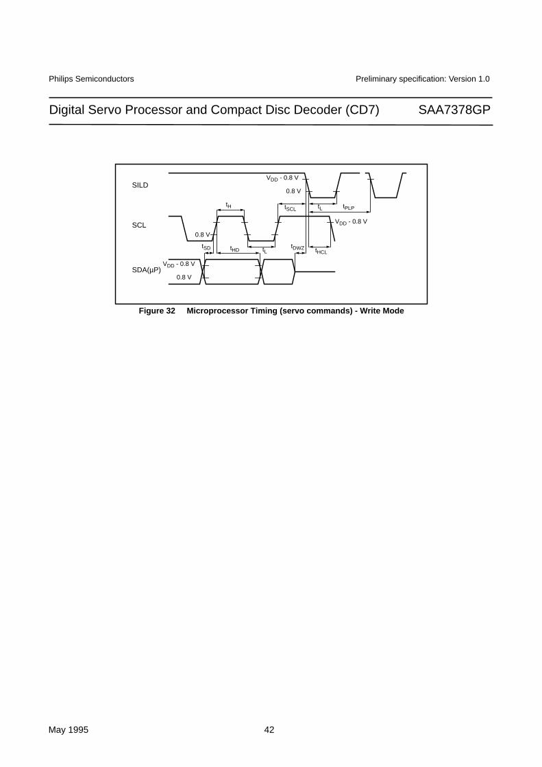
Note that: - RAB must be held low.- The command or data is interpreted by the SAA7378 after the high-low transition of SILD.- There must be a minimum time of 65µs between SILD pulses.
9.4.1 Writing Repeated Data In Servo CommandsThe same data byte can be can be repeated by applying extra SILD pulses as shown in Figure 26. SCL must stay high
RAB (µP)
SCL (µP)
SDA (SAA7378)
Read start allowed
10.8ms 15.4ms
2.3ms
CRC OK CRC OKHigh
impedance
Figure 23 SUBQREADY-I Status Timing when no Subcode is Read
RAB (µP)
SCL (µP)
SDA (SAA7378)Q1 Q2 Q3 Qn
t2t1 t3
Figure 24 SUBQREADY-I Status Timing when Subcode is Read

Philips Semiconductors Preliminary specification: Version 1.0
May 1995 29
Digital Servo Processor and Compact Disc Decoder (CD7) SAA7378GP
between the SILD pulses.
9.5 Read Servo CommandsA read data command is used to transfer data (status information) to the microprocessor, using the protocol shown in Figure27. The first byte written determines the type of command. After this byte a variable number of bytes can be read.Note that: - RAB must be held low.
- After the end of a read command there must be a delay of 65µs before a write command is started.- There must be a minimum time of 65µs between SILD pulses.
Figure 25 Microprocessor Protocol for Write Servo Commands
SILD (µP)
SCL (µP)
SDA (µP)
SDA (SAA7378)Hi-impedance
D7 D6 D5 D4 D3 D2 D1 D0Command or Data byte
SILD (µP)
Command Data1 Data2 Data3
SDA (µP)
Microprocessor write (one byte : command or data)
Microprocessor write (full command)
SDA (µP)
Figure 26 Microprocessor Protocol for Repeated Data in Write Servo Commands
SILD (µP)
Command Data1
Microprocessor write (full command)
SILD (µP)
SCL (µP)
SDA (µP)
D7 D6 D5 D4 D3 D2 D1 D0
Figure 27 Microprocessor Protocol for Read Servo Commands
Data byte
SDA (SAA7378)
Command
SDA (SAA7378)
Microprocessor read (one data byte)
Microprocessor read (full command)
SILD (µP)
Data1 Data2 Data3
Philips Semiconductors Preliminary specification: Version 1.0
May 1995 30
Digital Servo Processor and Compact Disc Decoder (CD7) SAA7378GP
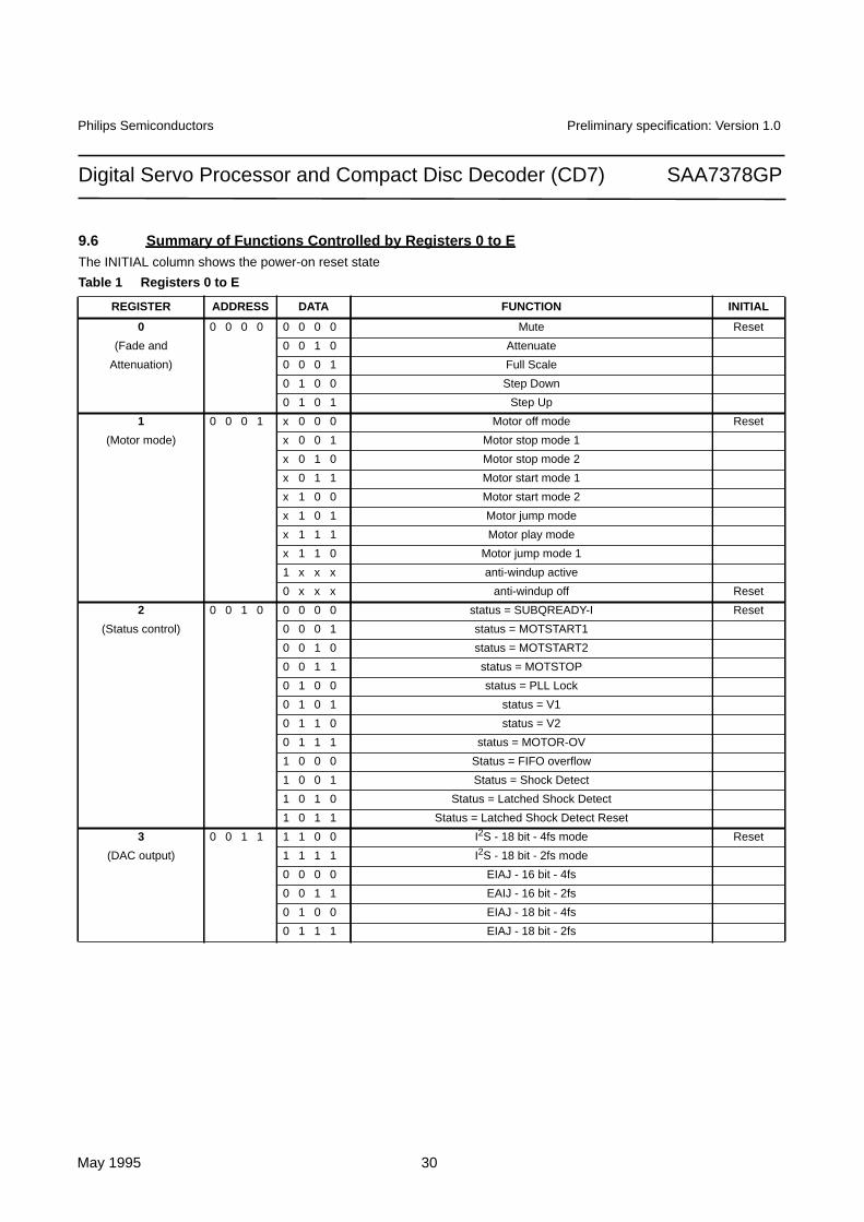
9.6 Summary of Functions Controlled by Registers 0 to EThe INITIAL column shows the power-on reset state
Table 1 Registers 0 to E
REGISTER ADDRESS DATA FUNCTION INITIAL
0 0 0 0 0 0 0 0 0 Mute Reset
(Fade and 0 0 1 0 Attenuate
Attenuation) 0 0 0 1 Full Scale
0 1 0 0 Step Down
0 1 0 1 Step Up
1 0 0 0 1 x 0 0 0 Motor off mode Reset
(Motor mode) x 0 0 1 Motor stop mode 1
x 0 1 0 Motor stop mode 2
x 0 1 1 Motor start mode 1
x 1 0 0 Motor start mode 2
x 1 0 1 Motor jump mode
x 1 1 1 Motor play mode
x 1 1 0 Motor jump mode 1
1 x x x anti-windup active
0 x x x anti-windup off Reset
2 0 0 1 0 0 0 0 0 status = SUBQREADY-I Reset
(Status control) 0 0 0 1 status = MOTSTART1
0 0 1 0 status = MOTSTART2
0 0 1 1 status = MOTSTOP
0 1 0 0 status = PLL Lock
0 1 0 1 status = V1
0 1 1 0 status = V2
0 1 1 1 status = MOTOR-OV
1 0 0 0 Status = FIFO overflow
1 0 0 1 Status = Shock Detect
1 0 1 0 Status = Latched Shock Detect
1 0 1 1 Status = Latched Shock Detect Reset
3 0 0 1 1 1 1 0 0 I2S - 18 bit - 4fs mode Reset
(DAC output) 1 1 1 1 I2S - 18 bit - 2fs mode
0 0 0 0 EIAJ - 16 bit - 4fs
0 0 1 1 EAIJ - 16 bit - 2fs
0 1 0 0 EIAJ - 18 bit - 4fs
0 1 1 1 EIAJ - 18 bit - 2fs

Philips Semiconductors Preliminary specification: Version 1.0
May 1995 31
Digital Servo Processor and Compact Disc Decoder (CD7) SAA7378GP
REGISTER ADDRESS DATA FUNCTION INITIAL
4 0 1 0 0 x 0 0 0 Motor gain G = 3.2 Reset
(Motor gain) x 0 0 1 Motor gain G = 4.0
x 0 1 0 Motor gain G = 6.4
x 0 1 1 Motor gain G = 8.0
x 1 0 0 Motor gain G = 12.8
x 1 0 1 Motor gain G = 16.0
x 1 1 0 Motor gain G = 25.6
x 1 1 1 Motor gain G = 32.0
0 x x x Disable comparator clock divider Reset
1 x x x Enable comparator clock divider; only if SELLPLL set high
5 0 1 0 1 x x 0 0 Motor f4 = 0.5Hz Reset
(Motor bandwidth) x x 0 1 Motor f4 = 0.7Hz
x x 1 0 Motor f4 = 1.4Hz
x x 1 1 Motor f4 = 2.8Hz
0 0 x x Motor f3 = 0.85Hz Reset
0 1 x x Motor f3 = 1.71Hz
1 0 x x Motor f3 = 3.42Hz
6 0 1 1 0 x x 0 0 Motor power max. 37% Reset
(Motor output x x 0 1 Motor power max. 50%
configuration) x x 1 0 Motor power max. 75%
x x 1 1 Motor power max. 100%
0 0 x x MOTO1, MOTO2 pins tri-state Reset
0 1 x x Motor PWM mode
1 0 x x Motor PDM mode
1 1 x x Motor CDV mode
7 0 1 1 1 x 0 0 0 DAC data normal value Reset
(DAC output) x 1 0 0 DAC data inverted value
0 x x x L channel first at DAC (WCLK normal) Reset
1 x x x R channel first at DAC (WCLK inverted)
Loop BW Hz Int. BW Hz Low-pass BW Hz
8 1 0 0 0 0 0 0 0 1640 525 8400
(PLL loop filter 0 0 0 1 3279 263 16800
bandwidth) 0 0 1 0 6560 131 33600
0 1 0 0 1640 1050 8400
0 1 0 1 3279 525 16800
0 1 1 0 6560 263 33600
1 0 0 0 1640 2101 8400
1 0 0 1 3279 1050 16800 Reset
1 0 1 0 6560 525 33600
1 1 0 0 1640 4200 8400
1 1 0 1 3279 2101 16800
1 1 1 0 6560 1050 33600
Table 1 Registers 0 to E

Philips Semiconductors Preliminary specification: Version 1.0
May 1995 32
Digital Servo Processor and Compact Disc Decoder (CD7) SAA7378GP
REGISTER ADDRESS DATA FUNCTION INITIAL
9 1 0 0 1 0 0 1 1 PLL loop filter equalisation Reset
(PLL equalisation) 0 0 0 1 PLL 30ns over-equalisation
0 0 1 0 PLL 15ns over-equalisation
0 1 0 0 PLL 15ns under-equalisation
0 1 0 1 PLL 30ns under-equalisation
A 1 0 1 0 x 0 1 0 Level II clock accuracy (<1000ppm) Reset
(EBU output) x 0 1 1 Level I clock accuracy (<50ppm)
x 1 1 0 Level III clock accuracy (>1000ppm)
x 1 1 1 EBU off - output low
0 x x x Flags in EBU off Reset
1 x x x Flags in EBU on
B 1 0 1 1 0 0 x x 33.8688MHz crystal present, or 8.4672MHz crystal with SELPLL set high
Reset
0 1 x x 16.9344MHz crystal present
x x 0 0 Standby 1 : ’CD-STOP’ mode Reset
x x 1 0 Standby 2 : ’CD-PAUSE’ mode
x x 1 1 Operating mode
C 1 1 0 0 x x x 1 External offtrack signal input at V1
(Versatile pins x x x 0 Internal offtrack signal used (V1 may be read via status) Reset
interface) x x 0 x Kill-L at KILL output, Kill-R at V3 output
0 0 1 x V3 = 0; single Kill output Reset
0 1 1 x V3 = 1; single Kill output
D 1 1 0 1 0 0 0 0 4-line motor (using V4, V5)
(Versatile pins x x 1 0 V4 = 0
interface) x x 1 1 V4 = 1 Reset
0 1 x x De-emphasis signal at V5, no internal de-emphasis filter
1 0 x x V5 = 0
1 1 x x V5 = 1 Reset
E 1 1 1 0 0 1 0 0 Motor brakes to 12% Reset
0 1 0 1 Motor brakes to 6%
Table 1 Registers 0 to E

Philips Semiconductors Preliminary specification: Version 1.0
May 1995 33
Digital Servo Processor and Compact Disc Decoder (CD7) SAA7378GP
9.7 Summary of Servo CommandsA list of the servo commands are given below; note that these are not fully backwards compatible with DSIC2:
Table 2 CD7 Servo Commands.
WRITE COMMANDS
code bytes parameters
Write_focus_coefs1 17h 7 <foc_parm3> <foc_int> <ramp_incr> <ramp_height> <ramp_offset> <FE_start><foc_gain>
Write_focus_coefs2 27h 7 <defect_parm> <rad_parm_jump> <vel_parm2> <vel_parm1> <foc_parm1><foc_parm2> <CA_drop>
Write_focus_command 33h 3 <foc_mask> <foc_stat> <shock_level>
Focus_gain_up 42h 2 <foc_gain> <foc_parm1>
Focus_gain_down 62h 2 <foc_gain> <foc_parm1>
Write_radial coefs 57h 7 <rad_length_lead> <rad_int> <rad_parm_play> <rad_pole_noise> <rad_gain><sledge_parm2> <sledge_parm_1>
Preset_Latch 81h 1 <chip_init>
Radial_off C1h 1 "1Ch"
Radial_init C1h 1 "3Ch"
Short_jump C3h 3 <tracks_hi> <tracks_lo> <rad_stat>
Long_jump C5h 5 <brake_dist> <sledge_U_max> <tracks_hi> <tracks_lo> <rad_stat>
Steer_sledge B1h 1 <sledge_level>
Preset_init 93h 3 <re_offset> <re_gain> <sum_gain>
Write_parameter A2h 2 <param_ram_addr> <param_data>
READ COMMANDS
code bytes parameters
Read_status 70h up to 5 <foc_stat> <rad_stat> <rad_int_lpf> <tracks_hi> <tracks_lo>
Read_aux_status F0h up to 3 <re_offset> <re_gain> <sum_gain>

Philips Semiconductors Preliminary specification: Version 1.0
May 1995 34
Digital Servo Processor and Compact Disc Decoder (CD7) SAA7378GP
9.7.1 Summary of Servo Command ParametersA list of the servo command parameters are given below:
parameter RAM addr. affects PORvalue
determines
foc_parm_1 - focus PID end of focus leaddefect detector enabling
foc_parm_2 - focus PID focus low passfocus error normalising
foc_parm_3 - focus PID focus lead lengthminimum light level
foc_int 14h focus PID focus integrator crossover freq
foc_gain 15h focus PID 70h focus PID loop gain
CA_drop 12h focus PID sensitivity of drop-out detector
ramp_offset 16h focus ramp assymetry of focus ramp
ramp_height 18h focus ramp p-p value of ramp voltage
ramp_incr - focus ramp slope of ramp voltage
FE_start 19h focus ramp minimum value of focus error
rad_parm_play 28h radial PID end of radial lead
rad_pole_noise 29h radial PID radial low-pass
rad_length_lead 1Ch radial PID length of radial lead
rad_int 1Eh radial PID radial integrator crossover freq
rad_gain 2Ah radial PID 70h radial loop gain
rad_parm_jump 27h radial jump filter during jump
vel_parm1 1Fh radial jump PI controller crossover freqs
vel_parm2 32h radial jump jump pre-defined profile
speed_threshold 48h radial jump maximum speed in fastrad mode
hold_mult 49h radial jump 00h sledge bandwidth during jump
brake_dist_max 21h radial jump max sledge distance allowed in fast actuatorsteered mode
sledge_long_brake 58h radial jump 7Fh brake distance of sledge
sledge_Umax - sledge voltage on sledge during long jump
sledge_level - sledge voltage on sledge when steered
sledge_parm_1 36h sledge sledge integrator crossover freq
sledge_parm_2 17h sledge sledge low pass freqssledge gainsledge operation mode
defect_parm - defect detector defect detector setting
shock_level - shock detector shock detector operation
chip_init - setup VRH level setting
xtra_preset 4Ah setup 38h laser on/offRA, FO, SL PDM modulating freq.
config_parm1 42h setup initialisation
config_parm2 53h setup initialisation
config_parm3 59h setup initialisation
config_parm4 68h setup initialisation

Philips Semiconductors Preliminary specification: Version 1.0
May 1995 35
Digital Servo Processor and Compact Disc Decoder (CD7) SAA7378GP
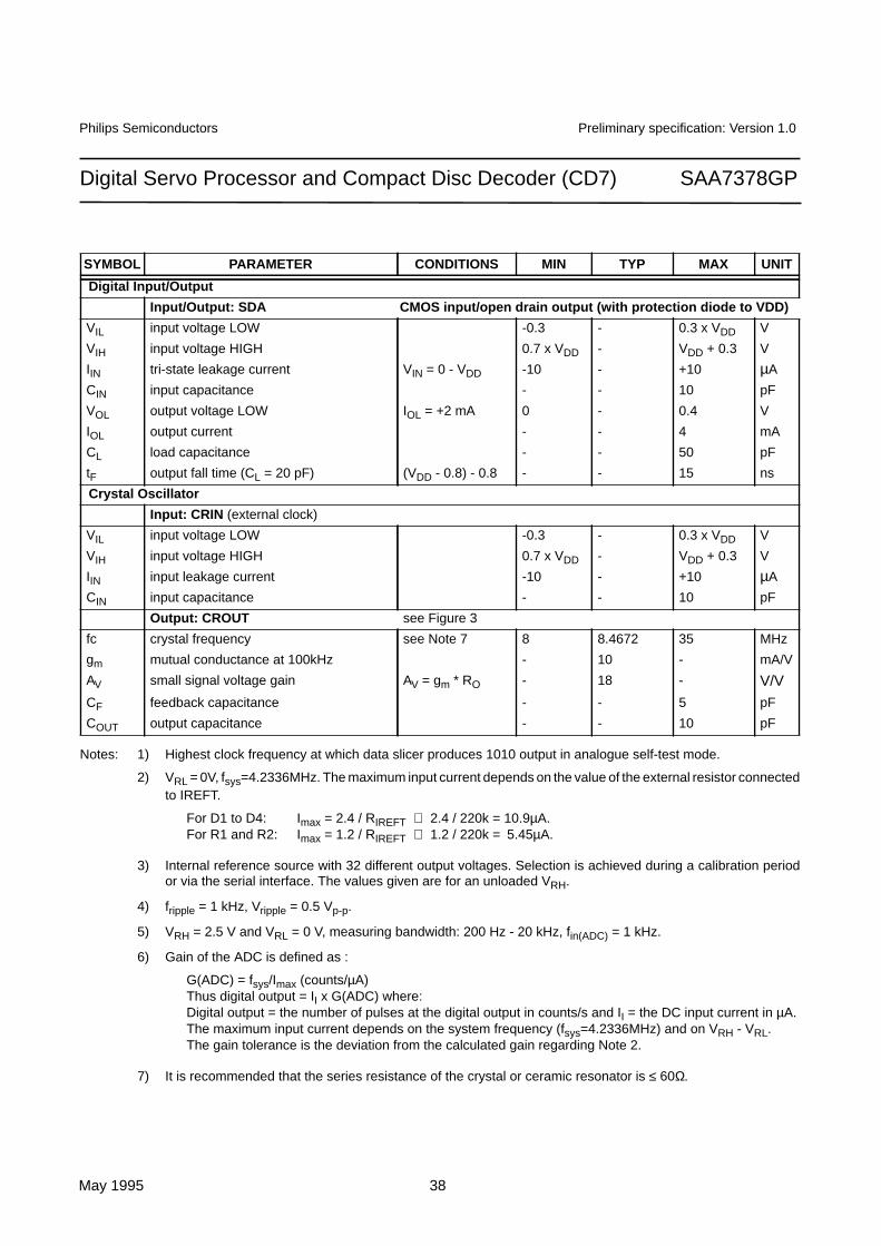
10. OPERATING CHARACTERISTICS
10.1 General CharacteristicsVDD = 3.4 to 5.5 V; VSS = 0; Tamb = 5 to 70 °C; unless otherwise stated.
SYMBOL PARAMETER CONDITIONS MIN TYP MAX UNIT
Supply
VDD supply voltage 3.4 5.0 5.5 V
IDD supply current VDD = 5 V - 49 mA
Decoder Analogue Front-End (VDD = 5.0 V; VSS = 0; Tamb = 25 °C)
Comparator Inputs, HFIN, HFREF:
fcomp clock frequency see Note 1 8 - 70 MHz
Vth switching thresholds 1.2 - VDD - 0.8 V
Vtpt HFIN input level 1.0 - V
Reference Generator, IREF:
VIREF reference voltage at IREF pin - VDD/2 - V
Servo Analogue Part (VDD = 5.0 V; VSS = 0; Tamb = 25 °C)
Pins D1, D2, D3, D4, R1, R2, VRH, VRL, IREFT:
IIREFT input current for IREFT 1.935 - 5.45 µA
RIREFT external resistor on IREFT 220 - 620 kΩVIREFT voltage on current input IREFT - 1.2 - V
ID maximum input current for centraldiode input signal
see Note 2 3.871 - 10.9 µA
IR maximum input current for satellitediode input signal
see Note 2 1.935 - 5.45 µA
VRL LOW level reference voltage 0 0 0 V
VRH HIGH level reference voltage see Note 3
output state 0 - 0.5 - V
output state v -30% .5*10v/44.4 +30% V
output state 31 - 2.5 - V
(THD+N)/S total harmonic distortion plus noise at 0 dB; see Note 5 - -50 -45 dB
S/N signal to noise ratio - 55 - dB
PSRR power supply rejection at VDDA2 see Note 4 - 45 - dB
Gtol gain tolerance see Note 6 -12 0 +12 %
∆G variation of gain between channels - - 2 %
a channel separation - 60 - dΒ

Philips Semiconductors Preliminary specification: Version 1.0
May 1995 36
Digital Servo Processor and Compact Disc Decoder (CD7) SAA7378GP
SYMBOL PARAMETER CONDITIONS MIN TYP MAX UNIT
Digital Inputs
Input: RESET, V1, V2, SELPLL CMOS input with pullup and hysteresis
VTHR switching threshold rising - - 0.8 x VDD V
VTHF switching threshold falling 0.2 x VDD - - V
Vhys hysteresis voltage - 0.33 x VDD - V
RPU input pull-up resistance VIN = 0 - 50 - kΩCIN input capacitance - - 10 pF
tRW reset pulse width (active low) RESET only 1 - - µs
Input: SCL, RAB, SILD CMOS input
VIL input voltage LOW -0.3 - 0.3 x VDD V
VIH input voltage HIGH 0.7 x VDD - VDD + 0.3 V
IIN input leakage current VIN = 0 - VDD -10 - +10 µA
CIN input capacitance - - 10 pF
Digital Output
Outputs: CL4
VOL output voltage LOW IOL = + 1 mA 0 - 0.4 V
VOH output voltage HIGH IOH = - 1 mA VDD - 0.4 - VDD V
CL load capacitance - - 25 pF
tR output rise time (CL = 20 pF) 0.8 to (VDD - 0.8) - - 20 ns
tF output fall time (CL = 20 pF) (VDD - 0.8) to 0.8 - - 20 ns
Outputs: CL16
VOL output voltage LOW IOL = +1 mA 0 - 0.4 V
VOH output voltage HIGH IOH = -1 mA VDD - 0.4 - VDD V
CL load capacitance - - 50 pF
tR output rise time (CL = 20 pF) 0.8 - (VDD - 0.8) - - 15 ns
tF output fall time (CL = 20 pF) (VDD - 0.8) - 0.8 - - 15 ns
Outputs: V4, V5
VOL output voltage LOW (VDD = 4.5 to 5.5 V) IOL = + 10 mA 0 - 1.0 V
output voltage LOW (VDD = 3.4 to 5.5 V) IOL = + 5 mA 0 - 1.0 V
VOH output voltage HIGH (VDD = 4.5 to 5.5 V) IOH = -10 mA VDD - 1 - VDD V
output voltage HIGH (VDD = 3.4 to 5.5 V) IOH = -5 mA VDD - 1 - VDD V
CL load capacitance - - 50 pF
tR output rise time (CL = 20 pF) 0.8 - (VDD - 0.8) - - 10 ns
tF output fall time (CL = 20 pF) (VDD - 0.8) -0.8 - - 10 ns

Philips Semiconductors Preliminary specification: Version 1.0
May 1995 37
Digital Servo Processor and Compact Disc Decoder (CD7) SAA7378GP
Open Drain Outputs
Outputs: CFLG, STATUS, KILL, V3,LDON
Open drain output with protection diode to VDD
VOL output voltage LOW IOL = +1 mA 0 - 0.4 V
IOL output current - - 2 mA
CL load capacitance - - 25 pF
tF output fall time (CL = 20 pF) (VDD - 0.8) - 0.8 - - 30 ns
Tri-State Outputs
Outputs: SCLK, WCLK, DATA, CL11
VOL output voltage LOW IOL = +1 mA 0 - 0.4 V
VOH output voltage HIGH IOH = -1 mA VDD - 0.4 - VDD V
CL load capacitance - - 50 pF
tR output rise time (CL = 20 pF) 0.8 - (VDD - 0.8) - - 15 ns
tF output fall time (CL = 20 pF) (VDD - 0.8) - 0.8 - - 15 ns
IIN tri-state leakage current VIN = 0 - VDD -10 - +10 µA
Output: CL11
tHIGH output high time (relative to clock period) VO = 1.5 V 45 50 55 %
Outputs: RA, FO, SL
VOL output voltage LOW IOL = +1 mA 0 - 0.4 V
VOH output voltage HIGH IOH = -1 mA VDD - 0.4 - VDD V
CL load capacitance - - 25 pF
tR output rise time (CL = 20 pF) 0.8 - (VDD - 0.8) - - 20 ns
tF output fall time (CL = 20 pF) (VDD - 0.8) - 0.8 - - 20 ns
IIN tri-state leakage current VIN = 0 - VDD -10 - +10 µA
Outputs: MOTO1, MOTO2, DOBM
VOL output voltage LOW (VDD = 4.5 to 5.5 V) IOL = +10 mA 0 - 1.0 V
output voltage LOW (VDD = 3.4 to 5.5 V) IOL = +5 mA 0 - 1.0 V
VOH output voltage HIGH (VDD = 4.5 to 5.5 V) IOH = -10 mA VDD - 1 - VDD V
output voltage HIGH (VDD = 3.4 to 5.5 V) IOH = -5 mA VDD - 1 - VDD V
CL load capacitance - - 50 pF
tR output rise time (CL = 20 pF) 0.8 - (VDD - 0.8) - - 10 ns
tF output fall time (CL = 20 pF) (VDD - 0.8) -0.8 - - 10 ns
IIN tri-state leakage current VIN = 0 - VDD - 10 - +10 µA
SYMBOL PARAMETER CONDITIONS MIN TYP MAX UNIT
Philips Semiconductors Preliminary specification: Version 1.0
May 1995 38
Digital Servo Processor and Compact Disc Decoder (CD7) SAA7378GP
Notes: 1) Highest clock frequency at which data slicer produces 1010 output in analogue self-test mode.
2) VRL = 0V, fsys=4.2336MHz. The maximum input current depends on the value of the external resistor connectedto IREFT.
For D1 to D4: Imax = 2.4 / RIREFT ⇒ 2.4 / 220k = 10.9µA.For R1 and R2: Imax = 1.2 / RIREFT ⇒ 1.2 / 220k = 5.45µA.
3) Internal reference source with 32 different output voltages. Selection is achieved during a calibration periodor via the serial interface. The values given are for an unloaded VRH.
4) fripple = 1 kHz, Vripple = 0.5 Vp-p.
5) VRH = 2.5 V and VRL = 0 V, measuring bandwidth: 200 Hz - 20 kHz, fin(ADC) = 1 kHz.
6) Gain of the ADC is defined as :
G(ADC) = fsys/Imax (counts/µA)Thus digital output = II x G(ADC) where:Digital output = the number of pulses at the digital output in counts/s and II = the DC input current in µA.The maximum input current depends on the system frequency (fsys=4.2336MHz) and on VRH - VRL.The gain tolerance is the deviation from the calculated gain regarding Note 2.
7) It is recommended that the series resistance of the crystal or ceramic resonator is ≤ 60Ω.
SYMBOL PARAMETER CONDITIONS MIN TYP MAX UNIT
Digital Input/Output
Input/Output: SDA CMOS input/open drain output (with protection diode to VDD)
VIL input voltage LOW -0.3 - 0.3 x VDD V
VIH input voltage HIGH 0.7 x VDD - VDD + 0.3 V
IIN tri-state leakage current VIN = 0 - VDD -10 - +10 µA
CIN input capacitance - - 10 pF
VOL output voltage LOW IOL = +2 mA 0 - 0.4 V
IOL output current - - 4 mA
CL load capacitance - - 50 pF
tF output fall time (CL = 20 pF) (VDD - 0.8) - 0.8 - - 15 ns
Crystal Oscillator
Input: CRIN (external clock)
VIL input voltage LOW -0.3 - 0.3 x VDD V
VIH input voltage HIGH 0.7 x VDD - VDD + 0.3 V
IIN input leakage current -10 - +10 µA
CIN input capacitance - - 10 pF
Output: CROUT see Figure 3
fc crystal frequency see Note 7 8 8.4672 35 MHz
gm mutual conductance at 100kHz - 10 - mA/V
AV small signal voltage gain AV = gm * RO - 18 - V/VCF feedback capacitance - - 5 pF
COUT output capacitance - - 10 pF

Philips Semiconductors Preliminary specification: Version 1.0
May 1995 39
Digital Servo Processor and Compact Disc Decoder (CD7) SAA7378GP
10.2 Operating Characteristics (I2S T iming)VDD = 3.4 to 5.5 V; VSS = 0; Tamb = 5 to 70 °C; unless otherwise stated.
SYMBOL PARAMETER CONDITIONS MIN TYP MAX UNIT
I2S Timing; see Figure 28
Clock output: SCLK (CL = 20pF)
tPO output clock period sample rate = fssample rate = 2 fssample rate = 4 fs
---
472.4236.2118.1
---
nsnsns
tHC clock HIGH time sample rate = fssample rate = 2 fssample rate = 4 fs
1668342
---
---
nsnsns
tLC clock LOW time sample rate = fssample rate = 2 fssample rate = 4 fs
1668342
---
---
nsnsns
Outputs: WCLK, DATA, EF (CL = 20pF)
tST setup time sample rate = fssample rate = 2 fssample rate = 4 fs
954824
---
---
nsnsns
tHT hold time sample rate = fssample rate = 2 fssample rate = 4 fs
954824
---
---
nsnsns
Figure 28 I 2S Timing
0.8 V
VDD-0.8 V
VDD-0.8 V
0.8 V
clock period tPO
tHCtLC
tHT tST
SCLK
WCLK
DATA
EF

Philips Semiconductors Preliminary specification: Version 1.0
May 1995 40
Digital Servo Processor and Compact Disc Decoder (CD7) SAA7378GP
10.3 Operating Characteristics ( µP Interface T iming)VDD = 3.4 to 5.5 V; VSS = 0; Tamb = 5 to 70 °C; unless otherwise stated.
Notes: 1) Negative set-up time means that the data may change after clock transition.
SYMBOL PARAMETER CONDITIONS MIN TYP MAX UNIT
µP interface timing (writing to registers 0 to F; reading Q-channel subcode and decoder status) seeFigure 29 and Figure 30.
Inputs SCL and RAB
tL input LOW time 500 - - ns
tH input HIGH time 500 - - ns
tR rise time - - 480 ns
tF fall time - - 480 ns
Read mode (CL = 20pF)
tDRD delay time RAB to SDA valid - - 50 ns
tDD propagation delay SCL to SDA 700 - 980 ns
tDRZ delay time RAB to SDA hi-impedance - - 50 ns
Write mode (CL = 20pF)
tSD setup time SDA to SCL note 1 -700 - - ns
tHD hold time SCL to SDA - - 980 ns
tSCR setup time SCL to RAB 260 - - ns
tDWZ delay time SDA hi-impedance to RAB 0 - - ns
µP interface timing (servo commands) see Figure 31 and Figure 32.
Inputs SCL and SILD
tL Input LOW time 710 - - ns
tH Input HIGH time 710 - - ns
tR rise time - - 240 ns
tF fall time - - 240 ns
Read mode (CL = 20pF)
tDLD delay time SILD to SDA valid - - 25 ns
tDD propogation delay SCL to SDA - - 950 ns
tDLZ delay time SILD to SDA hi-impedance - - 50 ns
Write mode (CL = 20pF)
tSD set up time SDA to SCL 0 - - ns
tHD hold time SCL to SDA 950 - - ns
tSCL aet up time SCL to SILD 480 - - ns
tHCL hold time SILD to SCL 120 - - ns
tPLP delay between two SILD pulses 65 - - µs
tDWZ delay time SDA hi-impedance to SILD 0 - - ns

Philips Semiconductors Preliminary specification: Version 1.0
May 1995 41
Digital Servo Processor and Compact Disc Decoder (CD7) SAA7378GP
Figure 29 Microprocessor Timing (Q-channel subcode and decoder statusinformation) - Read Mode
RAB
SCL
SDA(SAA7378)
tDRZ
tDRDtDD
0.8 V
0.8 V
VDD - 0.8 V
VDD - 0.8 V
VDD - 0.8 V
0.8 V
tRtR tF
tF
Figure 30 Microprocessor Timing (Registers 0 to E) - Write Mode
RAB
SCL
SDA(µP)
tSD
0.8 V
0.8 V
VDD - 0.8 V
VDD - 0.8 V
tHD
tSCR tL
VDD - 0.8 V
tDWZtL
tH
0.8 V
tH
Figure 31 Microprocessor Timing (servo commands) - Read Mode
SILD
SCL
SDA(SAA7378)
tDLZ
tDLD
tDD
0.8 V
0.8 V
VDD - 0.8 V
VDD - 0.8 V
Philips Semiconductors Preliminary specification: Version 1.0
May 1995 42
Digital Servo Processor and Compact Disc Decoder (CD7) SAA7378GP
Figure 32 Microprocessor Timing (servo commands) - Write Mode
SILD
SCL
SDA(µP)
tPLP
tSD
0.8 V
0.8 V
VDD - 0.8 V
VDD - 0.8 V
tHD
tSCL tL
VDD - 0.8 V
tHCLtDWZtL
tH
0.8 V

Philips Semiconductors Preliminary specification: Version 1.0
May 1995 43
Digital Servo Processor and Compact Disc Decoder (CD7) SAA7378GP
11. APPLICATION INFORMATION
Fig
ure
33
Typ
ical
SA
A73
78 a
pplic
atio
n di
agra
m
SA
A73
78
VS
SA1
VD
DA1
D1
D2
D3
VR
L
D4
R1
R2
IRE
FT
VR
H
VS
SA2
SE
LPLL
ISLI
CE
HF
IN
VS
SA3
V2
V1
CFLG
TEST10
VDD3C
TEST9
RESET
VSS4
41
SILD
RAB
SCL
SDA
CL4
LDO
N
HF
RE
F
IREF
VDDA2
TEST1
CRIN
CROUT
TEST2
CL16
CL11
RA
FO
SL
TEST3
VDD1P
DOBM
SC
LK
VD
D2 P
WC
LK
DA
TA
TE
ST
8
KIL
L
V3
V4
V5
VS
S2
TE
ST
7
TE
ST
6
TE
ST
5
TE
ST
4
MO
TO
2
MO
TO
1
VS
S3
VS
S1
3339 37 3447 44 43 40 38 36 3548 46 45 42
8 1610 12 152 5 6 9 11 13 141 3 4 7
24
32
26
28
31
18
21
22
25
27
29
30
17
19
20
23
57
49
55
53
50
63
60
59
56
54
52
51
64
62
61
58
+V
VD
DA
+
2.2Ω
100n
F33
µF
220p
F
220p
F
220p
F10
0kΩ
100k
Ω22
0pF 22
0pF
220p
F
VD
DA
100n
F
22nF
100n
F
47pF
22kΩ
270k
Ω
2.2k
Ω2.
2nF
to p
ower
ampl
ifier
sto
DO
BM
tran
sfor
mer
mic
ro-c
ontr
olle
rin
terf
ace
to DA
C
100n
F
mot
orin
terf
ace
VD
D
+V
+V
+V
VD
D
VD
D
2.2Ω
33µF
+
4.7k
Ω4.
7kΩ
100n
F
2.2Ω
100n
F
2.2Ω 10
0nF
(1)
(2)
D4
3
RF
E
D2
D3
D1
D5
D6
LDO
N
254 9167
TD
A13
00
(1)
Dia
gram
is fo
r a
5V a
pplic
atio
n. F
or 3
.4V
app
licat
ions
an
addi
tiona
l res
isto
r of
150
kΩ s
houl
d be
add
ed b
etw
een
IRE
F (
pin
18)
and
grou
nd.
(2)
For
cry
stal
osc
illat
or c
ircui
t see
Fig
ure
3.
(3)
The
con
nect
ions
to T
DA
1300
are
sho
wn
for
sing
le fo
ucau
lt m
echa
nism
s.
(3)

Philips Semiconductors Preliminary specification: Version 1.0
May 1995 44
Digital Servo Processor and Compact Disc Decoder (CD7) SAA7378GP
12. PACKAGE OUTLINE
Fig
ure
34
64-
lead
qua
d fla
t-pa
ck; p
last
ic (
SO
T39
3-1)

Philips Semiconductors Preliminary specification: Version 1.0
May 1995 45
Digital Servo Processor and Compact Disc Decoder (CD7) SAA7378GP
13. SOLDERING
13.1 Plastic quad flat-packs
13.1.1 BY WAVEDuring placement and before soldering, the component must be fixed with a droplet of adhesive. After curing the adhesive,the component can be soldered. The adhesive can be applied by screen printing, pin transfer or syringe dispensing.Maximum permissible solder temperature is 260 ºC, and maximum duration of package immersion in solder bath is 10 s, ifallowed to cool to less than 150 ºC within 6 s. Typical dwell time is 4 s at 250 ºC.A modified wave soldering technique is reccommended using two solder waves (dual-wave), in which a turbulent wave withhigh upward pressure is followed by a smooth laminar wave. Using a mildly-activated flux eliminates the need for removalof corrosive residues in most applications.
13.1.2 BY SOLDER PASTE REFLOWReflow soldering requires the solder paste (a suspension of fine solder particles, flux and binding agent) to be applied to thesubstrate by screen printing, stencilling or pressure-syringe dispensing before device placement.Several techniques exist for reflowing; for example, thermal conduction by heated belt, infrared, and vapour-phase reflow.Dwell times vary between 50 and 300 s according to method. Typical reflow temperatures range from 215 to 250 ºC.Prehaeting is necessary to dry the paste and evaporate the binding agent. Preheating duration: 45 min at 45 ºC.
13.1.3 REPAIRING SOLDERED JOINTS (BY HAND-HELD SOLDERING IRON OR PULSE-HEA TEDSOLDER TOOL)
Fix the component by first soldering two, diagonally opposite, end pins. Apply the heating tool to the flat part of the pin only.Contact time must be limited to 10 s at up to 300 ºC. When using proper tools, all other pins can be soldered in one operationwithin 2 to 5 s at between 270 and 320 ºC. (Pulse-heated soldering is not recommended for SO packages.)For pulse-heated solder tool (resistance) soldering of VSO packages, solder is applied to the substrate by dipping or by anextra thick tin/lead plating before package placement.
14. DEFINITIONS
15. LIFE SUPPORT APPLICA TIONSThese products are not designed for use in life support appliances, devices, or systems where malfunction of these productscan reasonably be expected to result in personal injury. Philips customers using or selling these products for use in suchapplications do so at their own risk and agree to fully indemnify Philips for any damages resulting from such improper useor sale.
Data sheet status
Objective specification This data sheet contains target or goal specifications for product development.
Preliminary specification This data sheet contains preliminary data; supplementary data may be published later
Product specification This data sheet contains final product specifications.
Limiting values
Limiting values are given in accordance with the Absolute Maximum Rating System (IEC 134). Stress above one ormore of the limiting values may cause permanent damage to the device. These are stress ratings only and operation ofthe device at these or at any other conditions above those given in the Characteristics sections of the specification is notimplied. Exposure to limiting values for extended periods may affect device reliability.
Application information
Where application information is given, it is advisory and does not form part of the specification.