real-time fpga implementation of a digital self
TRANSCRIPT

Vesa Lampu
REAL-TIME FPGA IMPLEMENTATIONOF A DIGITAL SELF-INTERFERENCE
CANCELLER IN AN INBAND FULL-DUPLEX TRANSCEIVER
Faculty of Information Technology and Communication SciencesMaster of Science Thesis
September 2019

i
ABSTRACT
VESA LAMPU: Real-time FPGA Implementation of a Digital Self-interferenceCanceller in an Inband Full-duplex TransceiverTampere University of technologyMaster of Science Thesis, 55 pages, 11 Appendix pagesSeptember 2019Master’s Degree Programme in Electrical EngineeringMajor: ElectronicsExaminers: D. Sc. (Tech) Lauri Anttila, Prof. Mikko Valkama
Keywords: real-time, full-duplex, nonlinear, FPGA, self-interference, canceller,digital
Full-duplex is a communications engineering scheme that allows a single device to trans-mit and receive at the same time, using the same frequency for both tasks. Compared totraditionally used half-duplex, where the transmission and reception is divided temporallyor spectrally, the spectral efficiency may theoretically be doubled in full-duplex opera-tion. However, the technology suffers from a profound problem, namely the self-interfer-ence (SI) signal, which is the name given to the signal a node transmits and simultane-ously also receives. Making the full-duplex technology feasible demands that the SI sig-nal is mitigated with SI cancellers. Such cancellers reconstruct an estimate of the SI signaland subtract the estimate from the received signal, thus suppressing the SI. For the SIsignal to be diminished as much as possible, canceller solutions should be deployed inboth analog and digital domains. This thesis presents a digital real-time implementationof a novel nonlinear self-interference canceller, based on splines interpolation. This can-celler utilizes a Hammerstein model to identify the SI signal, taking advantage of a FIRfilter for the identification of the SI channel, and splines interpolation to model the non-linear effects of the transceiver circuitry. The new canceller solution promises great re-duction in computational complexity compared to traditional algorithms with little to nosacrifice in cancellation performance.
The algorithm was implemented for a National Instruments USRP SDR device using Lab-VIEW Communications System Design Suite 2.0. The LabVIEW program provides therequired connectivity to the USRP platform, as the SDR lacks a user interface. In addition,the functionality of the SDR is determined in LabVIEW, by creating code that is then runon the USRP, or more specifically, on the built-in FPGA of the device. The FPGA iswhere the SI canceller is executed, in order to ensure real-time operation. Even thoughthe USRP device employs a high-end FPGA with plenty of resources, the canceller im-plementation needs to be simplified nonetheless, for example by approximating magni-tudes of complex values and by decreasing the sample rate of the canceller. With thesimplifications, the implementation utilizes only 34.9 % of available slices on the FPGAand only 34.6 % of the DSP units. Measurements with the canceller show that it is capableof SI cancellation of up to 48 dB, which is on par with state-of-the-art real-time SI can-cellations in literature. Furthermore, it was demonstrated that the canceller is capable ofbidirectional communication in various circumstances.

ii
TIIVISTELMÄ
VESA LAMPU: Reaaliaikainen digitaalisen itseishäiriön vaimentajan FPGA to-teutus full-duplex lähetin-vastaanottimessaTampereen teknillinen yliopistoDiplomityö, 55 sivua, 11 liitesivuaSyyskuu 2019Sähkötekniikan diplomi-insinöörin tutkinto-ohjelmaPääaine: ElektroniikkaTarkastajat: TkT Lauri Anttila, Prof. Mikko Valkama
Avainsanat: reaaliaikainen, full-duplex, epälineaarinen, FPGA, itseishäiriö, vai-mennus, digitaalinen
Full-duplex on tietoliikenneratkaisu, jossa yksi laite lähettää ja vastaanottaa tietoa yhtä-aikaisesti, käyttäen samaa taajuutta. Verrattuna yleisesti käytettyihin half-duplex-ratkai-suihin, joissa lähetys ja vastaanotto on jaettu joko ajan tai taajuuden suhteen, full-duplex-toiminnassa voidaan spektrillinen tehokkuus teoreettisesti jopa tuplata. Full-duplex tek-nologia kärsii kuitenkin hyvin merkityksellisestä ongelmasta, niin kutsutusta itseishäiri-östä, eli signaalista, jonka laite lähettäessään myös samanaikaisesti vastaanottaa. Full-duplex-toiminnan edellytyksenä on, että itseishäiriötä vähennetään vastaanotetusta sig-naalista merkittävästi, käyttäen itseishäiriön vaimentajia. Näiden vaimentimien tarkoituson luoda mallin pohjalta itseishäiriösignaalista estimaatti, ja vähentää estimaatti vastaan-otetusta signaalista, jolloin itseishäiriö vaimenee. Vaimennuksen maksimoimiseksi vai-mentimia tulisi käyttää sekä analogisella, että digitaalisella puolella. Tässä työssä on esi-tetty uudenlaisen digitaalisen epälineaarisen itseishäiriön vaimenninratkaisun reaaliaika-toteutus. Tämä uusi vaimennin perustuu niin kutsuttuun spline-interpolointiin, hyödyn-täen Hammerstein mallia, jossa häiriökanava mallinnetaan FIR-filtterin ja lähettimen epä-lineaarisuudet spline-interpoloinnin avulla. Tämän uuden vaimentimen on tarkoitus ollalaskennallisesti huomattavasti kevyempi kuin aiemmat vastaavat algoritmit, samalla kui-tenkin vaimentavan itseishäiriötä yhtä tehokkaasti.
Algoritmi toteutettiin National Instrumentsin USRP SDR alustalle käyttäen LabVIEWCommunications System Design Suite 2.0:sta. LabVIEW tarjoaa rajapinnan USRP:n jatietokoneen välille, sillä USRP-laitteessa ei ole käyttöliittymää. Lisäksi USRP:n toimintamääritetään LabVIEW:ssa kirjoittamalla koodi, joka ajetaan USRP:n sisältämälläFPGA:lla. Varsinainen itseishäiriönvaimennin ajetaan juuri FPGA:lla reaaliaikaisuudentakaamiseksi. Vaikkakin USRP:n sisältämä FPGA:lla on suuri määrä resursseja, on vai-mennintoteutusta yksinkertaistettava, esimerkiksi estimoimalla kompleksiluvun magni-tudin ja alentamalla vaimentimen näytetaajuutta. Yksinkertaistuksien kanssa vaimenninkäyttää vain noin 34.9 % lohkoista ja vain 34.6 % DSP-yksiköistä. Mittaukset osoittivat,että vaimennin kykenee alentamaan itseishäiriötä jopa 48 dB, ollen näin alan huipputu-losten tasolla. Lisäksi osoitettiin, että vaimentimen avulla on mahdollista viestiä kaksi-suuntaisesti erilaisissa olosuhteissa.

iii
PREFACE
As I am writing this, more than a year has passed since I started working on my thesis.The project this thesis is based on was started in February 2018, and it was successfullycompleted at the end of the same year. One could argue that the thesis could have beenfinished a long time ago, and they would probably be right, as I have indeed taken mytime with it. Nevertheless, here I am writing the preface, and it is time to give credit whereit is due.
First and foremost, I would like to thank my supervisor Lauri Anttila for his excellentguidance throughout the project and thesis. It has definitely been a privilege working withhim, the amount of things I have learned this past year and a half is astounding. As mysupervisor, he has also been a huge factor in making the atmosphere of the work environ-ment enjoyable, which is something I am really grateful for. Of the senior scholars, Iwould also like to thank my thesis’ other examiner Mikko Valkama and Dani Korpi forproviding me with instructions and a nice place to work in.
I would like to give enormous thanks to my colleague Pablo Pascual Campo for helpingme along the way, and giving me support whenever I needed it. He also kept pushing meto finish the thesis, so it is in part thanks to him that I am writing this now, instead ofsometime in the future.
A special thankyou goes to one of my lecturers, Olli-Pekka Lundén, who sparked theinterest towards RF engineering in me. He is also the one who suggested me for the po-sition in the project. Additionally, Matias Turunen played a major role in the measure-ments, and I thank him for that. Seyed Ali Hassani of the KU Leuven University was ofgreat help with the LabVIEW code, big thanks to him as well.
Outside the academia, I would of course like to thank my family and especially my par-ents Taina and Tomi for providing me with the circumstances to reach this point, not justduring my studies, but also throughout my life. I know I do not say it often enough, but Ido appreciate everything you have done for me. My last thankyous go to all of my friends,family members and colleagues who were not mentioned, but who made the last six yearsof my life as enjoyable as they have been.
This work has received funding from the European Union's Horizon 2020 research andinnovation program under grant agreement No. 732174 (ORCA, Extension #4).
Tampere, September 16, 2019
Vesa Lampu

iv
CONTENTS
1. INTRODUCTION ................................................................................................ 12. RADIO COMMUNICATIONS SYSTEM BASICS .............................................. 4
2.1 In-phase and Quadrature Signals ................................................................. 52.2 Sampling and Resampling .......................................................................... 62.3 Wireless Inband Full-duplex Systems ......................................................... 8
3. NONLINEAR DIGITAL SELF-INTERFERENCE CANCELLER ..................... 113.1 Adaptive Linear Filtering .......................................................................... 12
3.1.1 LMS Algorithm Derivation ......................................................... 143.1.2 Finite Precision LMS .................................................................. 16
3.2 Splines Interpolation ................................................................................. 173.3 Adaptive Hammerstein Spline-based Self-Interference Canceller .............. 20
4. DEVELOPMENT ENVIRONMENT .................................................................. 234.1 USRP and FPGA ...................................................................................... 234.2 LabVIEW Communications System Design Suite 2.0 ............................... 25
5. IMPLEMENTATION ......................................................................................... 285.1 Complex Number Magnitude Approximation ........................................... 315.2 Delay Estimation ...................................................................................... 325.3 Target Code .............................................................................................. 335.4 Host Code ................................................................................................. 38
6. EXPERIMENTS AND RESULTS ...................................................................... 406.1 Signal-to-interference-plus-noise Ratio, Symbol Error Rate and Sum Rate 416.2 Functional Validation ............................................................................... 436.3 Bidirectional Full-duplex Operation .......................................................... 46
6.3.1 Line-of-sight case........................................................................ 476.3.2 Through the wall case ................................................................. 49
7. SUMMARY AND FUTURE WORK .................................................................. 53REFERENCES ........................................................................................................... 56
APPENDIX A: SI Canceller Loop
APPENDIX B: ‘SI Canceller’ VI
APPENDIX C: ‘Splines Estimation’ subVI
APPENDIX D: ‘Splines Row’ subVI
APPENDIX E: ‘q subarray’ subVI
APPENDIX F: ‘Linear Filter’ subVI
APPENDIX G: ‘Sum Array Elements’ subVI

v
APPENDIX H: ‘Splines Update’ subVI
APPENDIX I: ‘Splines x X*w’ subVI
APPENDIX J: UI of the Host Program
APPENDIX K: Host Code for Determining Delay and DC-offset

vi
LIST OF FIGURES
Figure 1. Visual representation of TDD and FDD half-duplex schemes. ................ 4Figure 2. Synthesis of xc(t) from xi(t) and xq(t) adapted from [52], p. 36. ............... 6Figure 3. A full-duplex transceiver with an RF canceller and a digital
canceller, adapted from [30], p. 19. ....................................................... 9Figure 4. A block diagram of an FIR filter. .......................................................... 13Figure 5. A block diagram presentation of an adaptive filter. .............................. 14Figure 6. The zeroth, first and second order B-splines basis functions for
uniform splines. .................................................................................... 19Figure 7. Block diagram of a Hammerstein system and the adaptive self-
interference canceller. .......................................................................... 20Figure 8. High-level schematic of a USRP device [45]. ....................................... 24Figure 9. Addition of two variables in LabVIEW.................................................. 26Figure 10. Overview of the FPGA transceiver loop, complete with the SI
canceller. ............................................................................................. 28Figure 11. Feedforward nodes in LabVIEW Communications 2.0. ......................... 29Figure 12. Reinterpret, cast to fixed-point and cast to complex fixed-point
nodes in LabVIEW Communications 2.0. .............................................. 30Figure 13. The real magnitude and the αMax+βMin approximation of the
magnitude of a normalized complex number. ........................................ 32Figure 14. The two setups used in the measurements: the two-antenna node
(left) the RF canceller node (right). ...................................................... 40Figure 15. Constellation of a 16-QAM alphabet, with the symbols shown. ............. 41Figure 16. Constellation of potential received symbols, supposed to represent
symbol 1001 in Figure 15. .................................................................... 42Figure 17. Power spectral densities in four measurement cases: Two-antenna
node with 8 dBm TX power (top left) and 16 dBm TX power (topright), and RF canceller node with 8 dBm TX power (bottom left)and 16 dBm TX power (bottom right). .................................................. 44
Figure 18. Inband cancellation of the SI signal with different transmit powersin both measurement cases. .................................................................. 45
Figure 19. SINR and SER of both nodes in half-duplex and full-duplexscenarios, with different transmit powers, the nodes in the sameroom. ................................................................................................... 47
Figure 20. Constellations of the received symbols in the two-antenna node, inHD (left) and in FD (right) operations with 12 dBm TX power, bothnodes in the same room. ....................................................................... 48
Figure 21. Sum rate with various TX powers in FD and HD operations, bothnode in the same room.......................................................................... 49

vii
Figure 22. SINR and SER of both nodes in half-duplex and full-duplexscenarios, with different transmit powers, the nodes separated by awall. ..................................................................................................... 50
Figure 23. Constellations of the received symbols in the two-antenna node, inHD (left) and FD (right) operations with 14 dBm TX power, nodesseparated by a wall .............................................................................. 51
Figure 24. Sum rate with various TX powers in HD and FD operations, nodesseparated by a wall .............................................................................. 51

viii
LIST OF SYMBOLS AND ABBREVIATIONS
1-D One DimensionalA/D Analog-to-DigitalCPU Central Processing UnitCSMA/CD Carrier Sense Multiple Access with Collision DetectionD/A Digital-to-AnalogdB DecibeldBm Decibel-milliwattDSP Digital Signal ProcessingEBD Electrical Balance DuplexerFD Full-duplexFDD Frequency Division DuplexingFIR Finite Impulse ResponseFPGA Field-Programmable Gate ArrayGHz GigahertzHD Half-duplexI In-phase componentIF Intermediate FrequencyIIR Infinite Impulse ResponseISM Industrial, Scientific and MedicalI/Q In-phase/QuadratureLabVIEW Laboratory Virtual Instrument Engineering WorkbenchLMS Least Mean-SquaresLO Local OscillatorLUT Lookup TableMHz Megahertzns NanosecondPA Power AmplifierOFDM Orthogonal Frequency-Division MultiplexingQ Quadrature-phase componentQAM Quadrature Amplitude ModulationRAM Random Access MemoryRC Resistor and CapacitorRF Radio FrequencyRLS Recursive Least-SquaresSDR Software Defined RadioSER Symbol Error RatioSI Self-InterferenceSINR Signal-to-Interference-plus-Noise RatioTDD Time division duplexingTX TransmitterUI User InterfaceUSRP Universal Software Radio PeripheralVI Virtual Instrument
1 Array of all onesA Amplitudea Real part of a complex numberB Amount of bits representing a value

ix
b Imaginary part of a complex numberBc Amount of bits in the filter coefficientsc Complex numberC Channel capacityC Spline basis matrixd Desired signald̄ Mean of desired signalDC DC-offsetE Statistical expectation operatore Error signalF A discrete signalfc Carrier frequencyfs Sampling frequencyG A discrete signalh Array representation of taps of a static FIR filterh Tap of a static FIR filterĥ Channel estimatehp Channel coefficients in the memory polynomial modeli Spline knot indexJ Cost functionj imaginary unitK Decimation factorL Interpolation factorl Lag introduced to a signal in finding the cross-correlationM Memory of a digital filterMpost Post-cursor taps of a digital filterMpre Pre-cursor taps of a digital filterN Number of symbols transmitted and receivedNe Amount of misinterpreted symbolsNi
P Spline basis function of order PNpp Number of partial productsp Cross-correlation vectorP Spline orderPmp Nonlinearity order of the memory polynomial modelQ Number of spline control pointsq Control points of the splines modelqim Imaginary part of complex spline control pointsqre Real part of complex spline control pointsR Autocorrelation matrixS Amount of samples in a signals Spline interpolated signalsi Ideal symbolsr Received symbols Vector containing past spline interpolated signalstx,i Spline knot on the x-axisu Spline abscissa valuew Impulse response of an adaptive filterX Diagonal matrix containing past values of xx Array representation of FIR filter inputsx Input signal for FIR filter/SI canceller

x
xe Complex envelope of a signalxSI SI model output in the memory polynomial modelxc Carrier wavexi In-phase component of xexq Quadrature component of xexw Element of array X*(n)w(n)y Output of the FIR filter/Hammerstein modelz̃ Memory polynomial model imperfectionα Term used for complex value magnitude approximationβ Term used for complex value magnitude approximationγ Coefficient dependent on rounding modeΔx Distance between spline knotsδ Weight value used for DC-offset determinationθ Phase of signalλ Small term to be added for leakage factorλmax Maximum eigenvalue of autocorrelation matrixμ Step-size of adaptive FIR filter algorithmμq Step-size of spline control point updateμw Step-size of linear filter coefficient updateΣ Matrix collecting M past vectors Ψ as columnsΣ Element of matrix Σσ Error from quantization for a given valueσd Expected value of the mean square of the desired signalσe Error caused by quantization for signal eσn Error caused by quantization for noiseσx Error caused by quantization for signal xφ Spline interpolation curveΨ Array containing the spline basis function indexed at iψ Basis function in the memory polynomial model
1
1. INTRODUCTION
Full-duplex is a communications engineering scheme where a single device both trans-mits and receives information at the same time, at the same frequency. Practically allmodern consumer devices nowadays are half-duplex devices, in which transmission andreception are divided by either time or frequency [16, pp. 453—454]. Traditionally, full-duplex technology has been seen very difficult to implement, due to the so-called self-interference signal [10]. The signal that a full-duplex device transmits, it naturally alsoreceives, and this received signal is called the self-interference signal. The self-interfer-ence is orders of magnitude greater in power than the actual desired signals transmittedfrom other devices, and thus in order to utilize full-duplex operation, the self-interferencesignal has to be mitigated [28]. This mitigation has long been the bottleneck for the com-mercialization of full-duplex devices, however, in recent years leaps in the technologyhave been made. With full-duplex technology, spectral efficiency can be theoreticallydoubled compared to traditional half-duplex schemes, which is a significant matter con-sidering the low amount of free frequency channels. Full-duplex can also, among otherthings, solve the well-known hidden node problem [40]. The upsides of full-duplex makeit an attractive choice for future communication systems.
The cancellation of the self-interference signal can be divided into two broad categories:analog and digital cancellation [25]. As the names suggest, the analog implementationsfunction in the analog domain, and the digital ones in the digital domain. On their own,neither implementation is sufficient in the cancellation of the self-interference. Thus, forthe technology to be feasible, both are needed to achieve sufficient cancellation. Duplex-ers can be counted as analog self-interference cancellers, even though strictly speakingthey do not cancel the self-interference, but rather just add isolation between the trans-mitter and receiver chains. In addition to duplexers, actual self-interference cancellers canbe implemented in the analog domain. In these implementations, an estimate of the re-ceived signal is formed from the transmit one, taking into account the channel effects onthe signal, and the estimate is subtracted from the received signal. The digital cancellersfunction on the same principle, but in the digital domain.
A digital self-interference canceller can be implemented in many environments. If thegoal is to make the system real-time, an option is to implement the algorithm on an FPGA,as is the case in this work. An FPGA, short for Field-programmable Gate Array, is areprogrammable microchip that can be programmed to execute a wanted algorithm. Thedifference between an FPGA and for example the central processing unit (CPU) of acomputer is that the program is translated into physical signals that propagate on theFPGA in parallel. The logical operations are achieved by generic logic gates that modernFPGA have in the order of tens of thousands. In addition to an FPGA, a full-duplex device

2
needs a transceiver. For this purpose, National Instruments’ USRP device is utilized. TheUSRP (Universal Software Radio Peripheral) is a software defined radio device, the func-tionality of which can be programmatically defined. The USRP has a transceiver circuitryin addition to an FPGA where the actual logic is executed. The USRP is controlled inLabVIEW Communications 2.0 environment. LabVIEW is a graphical programming lan-guage developed by National Instruments, in which the functionality is defined with func-tional blocks and wires connecting the blocks, rather than text as in traditional program-ming languages. LabVIEW Communications 2.0 is a standalone piece of LabVIEW soft-ware intended to be utilized in communications applications. Two separate codes aremade in LabVIEW Communications 2.0: a target code that defines the functionality ofthe FPGA and the USRP, and the host code, which collects and visualizes data from theUSRP and controls the target code. The host code is executed on a computer in LabVIEWCommunication 2.0. The target code is also made in the same program, but it is translatedinto a bit file, which is uploaded onto the USRP when the host code is run.
The implemented digital self-interference canceller is based on a novel spline-basedHammerstein model, introduced in [47]. The Hammerstein model is a cascaded discrete-time model, where a linear part follows a nonlinear one [41]. This structure emulates themodelled circuitry fairly well, with the nonlinear power amplifier (PA) followed by thelinear channel. The most notable source of nonlinearity is the transmitter PA [29], whichis driven close to the saturation point in order to maximize efficiency. By doing so, theamplifier causes noticeable nonlinear distortion on the transmit signal. In this implemen-tation, the nonlinear behavior is modelled using splines. Splines are piecewise definedpolynomial approximations, with certain continuity constraints between the pieces [3, p.11]. After the nonlinear power amplifier, the signal propagates through the channel, whichis modelled using a finite impulse response (FIR) filter. The response is controlled withthe filter coefficients. The output of the Hammerstein model is supposed to correspond tothe actual self-interference signal as closely as possible. The output is subtracted from thereceived signal, giving the error signal as a result. Both the splines and the linear filter areadaptive, and the coefficients of both are controlled with the information from the errorsignal. This algorithm is considerably lighter in terms of calculations required than pre-vious algorithms, which utilize memory polynomial models [47, 54].
The algorithm is implemented in LabVIEW Communications 2.0, as a part of an existingtransceiver code. The native frequency of the used USRP device is 120 MHz, and thetransceiver code runs at that frequency as well. Even though the self-interference cancel-ler is relatively light in computation, it still cannot be executed entirely within one clockcycle at that frequency. Furthermore, 120 MHz restricts the amount of operations that canbe done in one clock cycle, therefore the algorithm was decided to run at 60 MHz. Theoriginal algorithm still cannot be executed completely even at this lower rate, but thetiming constraints are easier to handle. The timing of the algorithm is done by means of
3
pipelining, which means that chosen intermediate values are stored in the FPGA’s regis-ters. The algorithm has seven pipelining stages in total, therefore it takes seven clockcycles for certain inputs to produce the corresponding output.
The system was tested by transmitting OFDM signals, which is a widely used waveformin telecommunications. The amount of cancellation the algorithm provides was tested intwo separate scenarios. In the first, the transmitter and receiver chains had their own an-tennas to isolate the chains. In the other scenario, a radio frequency (RF) canceller wasutilized and the chains shared an antenna. Both scenarios were measured at multiple dif-ferent transmit powers. The digital canceller is capable of providing up to around 48 dBof digital cancellation, when the system utilizes OFDM signals, with 10 MHz bandwidth,transmit at 2.4 GHz. With the RF canceller, the system is able to reduce the self-interfer-ence level close to the device’s noise floor. In addition to these tests, the two setups weretested in a real bidirectional full-duplex scenario. It turns out that the digital cancellermay be utilized in an actual communication device, as the information the other nodesends is decipherable, since the noise added by the full-duplex operation is manageable.Thus, the algorithm may someday be used in an actual consumer device.

4
2. RADIO COMMUNICATIONS SYSTEM BASICS
This chapter delves into the basic theoretical information needed to understand the func-tionality of communications systems. In order to modify the signal digitally, the signalhas to be represented in a discrete form. This means that the signal has to be sampled,which means taking a sample of the signal at predetermined intervals or at sampling fre-quency. It turns out that every sample of every signal can be represented with just twovalues, the in-phase (I) and quadrature (Q) components, and they can be joined togetherto form a complex valued number. The I- and Q-branches of the signal are at baseband,but the I/Q-modulator, which is responsible for the generation of the transmit signal,transforms the signals to passband centered on the carrier frequency [39, p. 3]. In thedigital domain, these values, or samples, present the continuous-time signal for a presettime, determined by the sampling frequency. The signal can be processed in the digitaldomain for example, to extract information from it, or, as it is the case in this thesis, tocancel the self-interference signal from it.
TX RX
fc
t
TX
RX
fc
tTDD FDD
Figure 1. Visual representation of TDD and FDD half-duplex schemes.
There are numerous ways to establish a link between two radio devices. The simplestmight be simplex, which means that one radio acts as a transmitter and the other as areceiver at all times. A bit more advanced technology is half-duplex, where both radioscan act as both transmitter and receiver. The transmission and reception in half-duplexdevices can be divided temporally or spectrally. Temporal or time division duplexing(TDD) allows the devices only to operate as a transmitter or a receiver at a time, while inspectral division or frequency division duplexing (FDD), a device acts as both transmitterand receiver at the same time, but in different frequency bands [20, p. 30]. Both TDD andFDD are conceptually presented in Figure 1. Taking the duplexing idea even further, in afull-duplex system both devices act as both transmitter and receiver simultaneously usingthe same frequencies. Using the same temporal and spectral resources allows more effi-cient data transmission, theoretically even doubling the spectral efficiency. However,full-duplex gives rise to a problem known as the self-interference signal, which has to be
5
minimized [10, 25, 28, 47]. The end of this chapter considers some benefits of the full-duplex scheme.
2.1 In-phase and Quadrature Signals
A communications system consists of a transmitter and a receiver at its simplest form.Between the two there is a path known as channel through which the signal propagatesfrom transmitter to receiver. The channel can be a wire or just air or free space, as is thecase with wireless communication [58, pp. 762—763].
In order to convey information through the channel, a signal is needed. This signal, thecarrier, can be an analog sinusoidal signal for example, although there are other optionsas well. The carrier on its own will not carry any information, but the information can beencoded to the carrier with modulation. In addition to allowing the information to be in-cluded to the carrier, modulation also allows the signal to be shifted in frequency, whichis desired especially in wireless communications. Three basic ways of analogue modula-tion are amplitude-, frequency-, and phase-modulation which affect the amplitude, fre-quency and phase of the carrier respectively [58, p. 767].
Let us consider an amplitude and phase modulated sinusoidal carrier wave ( ), whichcan be written as
( ) = ( ) 2 + ( ) , (1)
where ( ) is the amplitude of the signal over time, the constant carrier frequency and( ) the phase of the signal over time. Amplitude modulation encodes data to ( ) and
phase- and frequency-modulations encode it to ( ). By applying a trigonometric identityto Equation (1), the carrier can now be rewritten as
( ) = ( ) ( ) (2 ) − ( ) ( ) (2 ) (2)
( ) = ( ) (2 ) − ( ) (2 ) (3)
where ( ) represents the in-phase component and ( ) the quadrature component ofthe signal. Both of the components represent the amplitude of their respective sinusoidalsignals over time. These components can also simply be denoted as I and Q respectively.By applying Euler’s formula to Equation (3), the carrier can finally be written as
( ) = Re ( ) , (4)
where ( ) = ( )+ ( ) = ( ) ( ) is the complex envelope of the real bandpasssignal ( ). Equation (4) signifies that the signal ( ) can now be represented with thecomplex baseband signal ( ), no matter how the signal is modulated. This in turn im-plies that theoretically all analog signals at frequency can be represented only with the

6
in-phase and quadrature components. The synthesis for ( ) from ( ) and ( ) isillustrated in Figure 2 [52, p. 35]. The setup in Figure 2 is called an I/Q-modulator.
∿
x (t)
∑+
--90°
LO
i
x (t)q
x (t)c
Figure 2. Synthesis of xc(t) from xi(t) and xq(t) adapted from [52, p. 36].
Figure 2 shows that the I/Q data will be multiplied with the carrier in a mixer, such thatthe I-branch will be multiplied with just the carrier and the Q-branch with a 90 degreeshifted carrier. Thus, the I/Q data does not have to be at carrier frequency, as it is shiftedto the desired frequency. This process of synthesizing the transmitted signal is also calledupconversion, as the data signal is being converted to carrier frequency [52, p. 35]. Up-conversion of the signal requires the carrier to be phase shifted exactly 90 degrees, andthis is rarely the case. This problem causes an effect known as I/Q-imbalance or mis-match. The imbalance creates a mirror image of the signal in frequency domain, withrespect to the local oscillator (LO) frequency. In time domain, the I/Q-imbalance can bemodeled as a superposition of the baseband signal and its complex conjugate. The effectsof the imbalance can be digitally mitigated, however [60].
2.2 Sampling and Resampling
In order to perform digital signal processing, the analog signal of interest has to be con-verted to digital form. This is done by analog-to-digital (A/D) conversion. A/D conver-sion samples a continuous-time signal with continuous amplitude. The end result is a dis-crete set of samples that represent the signal for the whole duration of the sampling period.The amplitude of the samples is also discrete and bound with a lower and upper limit. Inother words, the samples are quantized [21, p. 101]. Quantization introduces distortion,often called quantization noise, to the signal since the samples rarely have the exact levelof the possible representations. That is why the samples values have to be rounded, trun-cated or by some other means assigned a value representable in the digital domain. Usingas many steps as possible for the outputs of the A/D converter decreases the effects ofquantization noise [46, pp. 27—28]. Additionally, quantizing the signal may lead theoutput to saturate if the sample’s value exceeds or drops below the maximum range ofthe possible outputs [26]. Once saturated, the output of the system will remain constant,

7
yielding either the maximum or the minimum representable value. Both the quantizationnoise and saturation have to be taken into account when translating the signals from ana-log and digital domain.
Since the sample representing the signal remains constant for a set period of time, thereis an upper-limit to which frequencies can be sampled with a certain sampling frequency.Conversely, there is a lower-limit to the sampling frequency when sampling a signal witha certain bandwidth. This lower-limit is known as the Nyquist frequency, and it is exactlyhalf of the sampling frequency of the system. Signals with frequencies higher than theNyquist frequency will be aliased, or mirrored with respect to the Nyquist frequency infrequency domain [44, p. 98]. Anti-aliasing filters restrict the input bandwidth of the inputsignals to satisfy the restriction imposed by the Nyquist frequency, which mitigates thealiasing effects in A/D converters.
In some instances, the sample rate of the signal has to be changed, in a process calledresampling. Changing the sample rate does not change the signal the sequence of valuesrepresents, but rather the amount of samples the sequence holds. Making the sample ratehigher is called interpolation and the reduction of it is called decimation [43, p. 305].Decimation by an integer factor is arguably the easiest of the operations to understand. Ifa signal, sampled at frequency fs, consists of S samples and the decimation factor is K,only every Kth sample from the original signal is kept, reducing the length of the signalto S/K. Thus, the sampling frequency is reduced to fs/K [14, pp. 72—73]. In order to pre-vent aliasing, the signal has to be low-pass filtered before decimation. A system that low-pass filters and decimates the signal is called a decimator [14, p. 89].
Interpolation, contrary to decimation, adds samples to the original signal. If the signalsampled at frequency fs again holds S samples and the interpolation factor is L, betweenevery sample L-1 zero samples will be added to the signal. This makes the signal’s newlength SL and the new sample rate is Lfs [14, pp. 97—98]. After adding the new values,their amplitudes have to be estimated. To achieve this, the signal has to be low-pass fil-tered, ideally using the sinc function. A simpler way for interpolation is it to linear inter-polate the values of the new samples, assuming the continuous-time signal does not haveany abrupt changes between the samples. Regardless of the execution, a system, whichadds zero samples to the signal and low-pass filters it, is called an interpolator [14, pp.103—110].
In addition to integer factors, interpolation and decimation are possible with non-integerfactors as well. Changing the sampling frequency by a rational number, which can bewritten as L/K, where both L and K are integers, can be achieved, conceptually, by inter-polating the signal by a factor of L and decimating it by a factor of K. It is also possibleto scale the sampling frequency by a non-rational value, but that is out of the scope of thisthesis.

8
2.3 Wireless Inband Full-duplex Systems
As it was stated at the beginning of the chapter, the simplest way to establish a radioconnection is to have a single transmitter and a single receiver. This type of configurationis named simplex. An example of a simplex system is a radio receiver, which only receivesthe signals that a broadcaster sends. While simplex definitely has its uses, it is more com-mon for radio systems to be duplex. Duplex means that all the devices connected to thesystem can act as both transmitter and receiver, a transceiver, which allows for two-waycommunication between the devices. Duplex can be divided into half-duplex and full-duplex. Half-duplex systems are either transmitters or receivers at a time over a certainresource, namely time or frequency. Full-duplex systems act as both transmitter and areceiver simultaneously while using the same resources [50, p. 672].
A prominent problem with full-duplex systems is the self-interference (SI) signal. Simul-taneously transmitting and receiving over the same frequency band causes SI. Naturally,by doing so the signal that is being transmitted is also being received by the same device.This received signal is the SI signal and it is often orders of magnitude greater in powerthan the desired received signals. Thus, the desired signals are drowned in the SI and areimpossible to decipher. Additionally, RF equipment is sensitive, especially on the re-ceiver side in order to pick up even the weakest signals. If the SI gets to the receivingchain unattenuated, the components might be damaged or destroyed all together [30, p.14].
Obviously, the SI signal needs to be attenuated or ideally cancelled completely. A way toachieve attenuation is to separate the transmitter and receiver chains, so that they do notshare a common antenna [10]. This method adds isolation between the chains, but ofcourse, the receiving antenna will still pick up some of the SI, but now it is attenuated.The same isolation effect can be achieved by using a duplexer, which now allows theusage of a shared antenna again. A duplexer separates the transmitting and receivingchains by routing the received signal from the antenna to the receiver and the signal fromthe transmit-chain to the antenna. The duplexer is most often a circulator, which is apassive device, but there are active duplexers as well, that require power and control fromoutside, such as an electrical balance duplexer (EBD) [37, 53]. Still, even with a duplexer,there is some leakage of the SI to the receiver since the isolation the duplexer provides isnot perfect. Additional cancellation of the SI is therefore required.
Figure 3 illustrates a simplified model of a full-duplex transceiver, completed with an RF-canceller and a digital canceller. The transmitter chain consists of a digital-to-analog con-verter, I/Q-modulator (discussed in Section 2.1), an amplifier and a bandpass filter. Afterthe transmitter chain, there is a power amplifier (PA), which amplifies the signal, in orderfor the receiver to be able to pick up the transmit signal. The receiver chain consists ofalmost the same components as the transmitter, except the I/Q-modulator is substitutedwith a demodulator and the digital-to-analog converter with an analog-to-digital one.

9
Both the transmitter and receiver chains share a common antenna, the utilization of whichis made possible by a circulator.
Transceiver
I/Q-modulator PA
I/Q-demodulator
I/QDAC
I/QADC
RF-cancellerDigitalcanceller
ITQT
IR
QR
IR+SI
QR+SI
Figure 3. A full-duplex transceiver with an RF canceller and a digital canceller,adapted from [30, p. 19].
The physical circuitry of the transceiver introduces imperfections and non-idealities tothe signals propagating through the system. Most notable of these effects, as far as SIcancellation is concerned, is the nonlinearity induced by the amplifiers. The most signif-icant source of nonlinearity is the PA on the output of the transmission chain, althoughother amplifiers and mixers of the system may add to it as well. Nonlinearity in the am-plifiers is caused by saturation, where high inputs do not yield as high outputs as it would,if the system was linear. Thus, the system becomes nonlinear. Although the distortion isunwanted, the amplifiers are still used close to the nonlinear region in order to maximizepower efficiency. Nonlinearity causes spectral regrowth, which can be seen in the spec-trum of the signal as “widening” of the signal at its base [15]. Other imperfections of thephysical circuitry include the I/Q-imbalance (discussed in Section 2.1) and quantizationnoise (discussed in Section 2.2).
The full-duplex transceiver introduced in Figure 3 contains two separate canceller blocksfor cancelling the SI signal. These are the RF-canceller and the digital canceller, whichfunction in the analog and digital domains respectively. Both of the blocks have a similarpurpose; they estimate the effects the coupling channel and distortion from the physicalcircuitry have on the signal, and subtract the estimate from the received signal [30, p. 3].This functionality is inherently different from the isolation that the duplexers provide,since isolation just prevents the transmit signal from leaking to the receiver, while thecancellation actually affects the received signal. Ideally, the estimate the canceller blockproduces matches the above-mentioned effects exactly and the SI signal is cancelled com-pletely. This is not the case with real signals however, hence there is some residual powerof the SI signal left over. Still, the power of the SI is decreased significantly and it is nowpossible to decipher the received signals of interest. The functionality of the digital can-celler will be explained in more detail in the following sections.
There are numerous benefits to using full-duplex systems, most notable one being thetheoretical doubling of spectral efficiency [1, 18]. This is due to both the receiver and the

10
transmitter using the same frequency, therefore doubling the amount of data that is trans-ferrable over the frequency band. As the frequency spectrum grows more and morecrowded, being able to use the available frequencies more efficiently becomes more andmore crucial. Full-duplex also simplifies the planning of links, as they only need onefrequency for operation [38, pp. 6—7].
A problem full-duplex offers a solution to is the hidden node problem. The hidden nodeproblem might occur when two devices try to contact a shared node, for example, whentwo Wi-Fi devices contact a wireless access point. The problem arises when the two clientnodes do not know of each other’s existence and send their data to the access point sim-ultaneously. The messages will then collide and the messages would have to be sent again,and the same issue might occur. The nodes know to send new messages by using theCarrier Sense Multiple Access with Collision Avoidance (CSMA/CA) protocol, even inhalf-duplex systems. However, even using CSMA/CA results in some packet losses [17].To combat this, a full-duplex system can be utilized. Full-duplex does not fix the issue onits own however, but rather it enables techniques that rely on simultaneous transmissionand reception to ultimately overcome the problem. These techniques introduce new ac-knowledgment schemes for the transmitter and receiver, introduced for example in [4]and [62]. The techniques are similar to CSMA/CD, but they utilize the full-duplex capa-bilities of the nodes to detect the collisions.
Full-duplex systems can also be used in wireless backhauling solutions. Backhauling re-fers to the way an access node is connected to the backbone network. For example in acellular phone case, the phones contact the base station, which acts as an access node andthe access node then connects, or backhauls, to other such nodes forming the backboneof the network [11, pp. 61—62]. Especially in locations with highly dense networks, us-ing wireless backhauling instead of wired one, the deployment costs are reduced. Full-duplex can be utilized for self-backhauling which means that the same frequency is usedfor the network’s uplinks and downlinks, and for the backhauling, which saves spectraland temporal resources [31].

11
3. NONLINEAR DIGITAL SELF-INTERFERENCECANCELLER
This chapter focuses on the theoretical aspects of a nonlinear digital self-interference can-celler and introduces a state-of-the-art implementation of such an algorithm. A nonlinearself-interference canceller, as opposed to a linear one, considers the nonlinear effects thephysical circuitry has on the signal. The most notable source of nonlinear distortion is thePA on the transmission chain, although other parts have nonlinear effects on the signal aswell. The digital SI canceller can be ultimately reduced to a simple subtraction, where thetransmitted signal is subtracted from the received signal. Unfortunately, it is not asstraightforward as that, since the received signal has passed through the channel and somecircuitry, so it is attenuated and distorted. Therefore, in order to cancel the received SI,the effects of the channel and the circuitry have on the signal have to be modelled. Thisproblem can be simplified a bit since the most prominent effects are those from the chan-nel and the nonlinearity the PA on the transmitter chain induces.
Traditionally, the effects from the channel and the nonlinearities are modeled in the digitaldomain using a memory polynomial model. The coefficients of the model take into ac-count the memory effects of the devices in use. This means that a single sample cannotsimply be handled independently as the previous values affect it as well. The memorypolynomial model of the self-interference signal can be written as
( ) = ℎ ( ) ( − ) + (̃ ) , (5)
where ( ) is the nth sample of the self-interference signal , the nonlinearityorder of the model, the length of the memory of the model, ℎ ( ) the channel coeffi-cients that include the memory of the PA, multipath channel and possible RF cancellation,
( − ) the th order basis function and (̃ ) the error from the imperfection ofthe model. In the digital canceller, the SI signal is approximated using (5), and the outputis subtracted from the received signal [2] to produce the error signal. If the model matchesthe effects perfectly, the error signal will be zero, and the SI is cancelled completely.However, there is always some residual power left from the SI, as the model is neverperfect.
The effects of the channel and the nonlinearities of the circuitry are hard to define, andthey can even change abruptly. That is why the coefficients of the model cannot be con-stant, but rather adaptive, which means that the coefficients of the model are updated atevery cycle of the algorithm. This is the most computationally demanding process of the

12
algorithm, as the actual cancellation can be reduced to mere multiplication of the coeffi-cients and the transmit signal, the product of which is then subtracted from the receivedsignal. The detailed formulas for the updates of the memory polynomial model are omit-ted here, but can be found for example in [32], where the update is achieved with the leastmean squares (LMS) method. Literature also has examples of the update of SI cancelleralgorithm being implemented using the recursive least squares (RLS) method, reportedfor example in [63].
As stated earlier, the nonlinear memory polynomial model incorporates the channel ef-fects and the nonlinearities in a single expression. However, it is also possible to decouplethese effects and model them separately, which makes them independent of one another.Thus, it is also possible to apply the updates to the model coefficients separately, and withdifferent paces, which might be desirable in some systems. The following sections focuson tools for modeling the channel and nonlinearities. These models are then used to definethe Hammerstein spline-based SI canceller.
3.1 Adaptive Linear Filtering
A physical filter is a frequency selective circuit that, ideally, only passes signals throughunattenuated and undistorted on wanted frequencies. A physical example of such a filteris an RC circuit, which, depending on the component arrangement, can act as a high-passor low-pass filter. The electrical properties of the components determine how the filterresponds to different frequencies. A digital filter does not comprise of physical compo-nents as it is just a mathematical algorithm, but it aims to accomplish the same as a phys-ical filter. Since the digital filter is just defined by some coefficients (discussed later), theresponse of the filter is easily adjustable. Furthermore, if the filter adjusts itself, the filterbecomes adaptive. Additionally, a digital filter can have a phase response that is com-pletely linear, a feat not possible for physical filters.
There are two basic classes of digital filters, infinite impulse response (IIR) and finiteimpulse response (FIR) filters. Out of the two classes, FIR has two major advantages overthe IIR in terms of linear filtering required in the SI canceller. First and most importantly,the FIR is inherently stable, so it does not require analysis to confirm the stability. Thisis especially handy for adaptive filters, as the changes in the coefficients could make anIIR filter unstable. Secondly, FIR can have exactly linear phase response (but not neces-sarily), whereas the IIR generally has a nonlinear phase response [24, p. 321]. Thus, theremainder of this section focuses on FIR filters.
FIR filtering for real valued signals is defined by the following expression:
( ) = ℎ( ) ( − ) , (6)

13
where ( ) is the th output of the filter, is the number of filter coefficients or taps,often referred to as the memory of the filter, ℎ( ) the th tap of the filter and ( − )the input delayed by steps. The variable ℎ also describes the impulse response of thefilter. The FIR filter can be presented in a block diagram, which clarifies the operation. Ablock diagram presentation of a FIR filter is presented in Figure 4.
z-1
z-1
z-1
Σ
( )
( − 1)
( − 2)
( − )
ℎ(0)
ℎ(1)
ℎ(2)
ℎ( )
( )
Figure 4. A block diagram of an FIR filter.
Figure 4 makes it clear that the output is dependent on past values and the presentvalue of and on the values of ℎ. Indeed, the performance of the filter is adjustable byvarying the coefficients of ℎ, as it is the only variable in the designer has direct access toin addition to the amount of taps in the filter [34, pp. 34—36]. For simplification, the pastand current values of and the values of ℎ can be compiled into separate vectors, =[ ( ) ( − 1)… ( − )] and = [ℎ(0) ℎ(1)… ℎ( )] . Now the FIR filteringoperation can be expressed as
( ) = , (7)
which is equivalent to Equation (6).
For a static filter, there are several methods for acquiring the values of to meet thecriteria of the design. These methods include the window method, the optimal methodand the frequency sampling methods, and they are among the most widely used proce-dures for filter design [24, p. 351]. These methods are computationally heavy however,and are designed to be only used once during the filter designing process. This is why theadaptive filtering takes another approach to determining the impulse response of the filter.These approaches include the least mean squares (LMS) and the recursive least squares(RLS) methods. Out of these two, the LMS offers less computational complexity and it is

14
the most widely used adaptive filter algorithm [34, p. 46; 9, p. 71]. Therefore, the remain-der of this chapter focuses on the LMS algorithm.
3.1.1 LMS Algorithm Derivation
A block diagram for an adaptive filter illustrated in Figure 5 shows two additional signalsneeded for the operation of the adaptive filter. These signals are the desired signal ( )and the error signal ( ).
FIR filter
Adaptivealgorithm
Σ_+( ) ( )
( )
( )
Figure 5. A block diagram presentation of an adaptive filter.
The desired signal presents the wanted behavior of the filter. It can be, for example, ameasured signal. The difference between the desired signal and the filter output, the errorsignal, is a measure of how well the filter follows the wanted behavior. Smaller errorsignal signifies better performance. With the information on the performance from theerror signal, the adaptive algorithm changes the filter coefficients accordingly [22, pp.96—97].
In order to generalize the adaptive filter solution, let us consider complex-valued signals.Thus, the FIR filter solution of Equation (7) can be written as
( ) = , (8)
where is the complex-valued impulse response of the filter (cf. , but for adaptivefilters is more common notation), and is the Hermitian transpose of . Now theerror signal can be written as [22, p. 205]
( ) = ( ) − ( ) = ( ) − . (9)
Now we may write a cost function for the filter [22, p. 97]:
( ) = [| ( )| ] = [ ( ) ∗( )], (10)

15
where is the statistical expectation operator. The LMS algorithm aims to minimize themean square error, which is where the name of the algorithm comes from. Equation (10)can be then further expanded using Equation (9) [22, p. 107; 49, p. 187]:
( ) = − − + , (11)
where is the expected value of the mean square of the desired signal ( ), =[ ∗( )] the cross-correlation vector between and ∗( ) and = [ ] the auto-
correlation matrix of the input. The minimization of the cost function is achieved withmethod of steepest descent, which means that the successive applied updates to the coef-ficients of the filter are done in the direction opposite of the gradient vector of the costfunction. The method of steepest descent is defined as [22, p. 204; 49, p. 186]
( + 1) = ( ) − ( ), (12)
where ( + 1) is the new impulse response of the filter, ( ) the current impulse re-sponse, the step-size or learning rate of the algorithm and ( ) the gradient vector ofthe cost function. The step-size is multiplied with a half for convenience that will be ap-parent later. The gradient of the cost function is [22, p. 206; 49, p. 187]
( ) = −2 + 2 ( ). (13)
In order to estimate the gradient, the simplest way is to substitute the vector and matrixwith their respective instantaneous estimates, = ∗( ) and = . Thus, the in-
stantaneous estimate for the gradient vector is given as [22, p. 236]
( ) = −2 ∗( )+ 2 ( ). (14)
Combining Equations (12) and (14), we get the following estimating expression for theupdate of the filter coefficients:
( + 1) = ( )+ ( ) ∗( ) − ( ) (15)
= ( )+ ( ) ∗( ). (16)
Equations (15) and (16) describe the LMS filter update algorithm [22, p. 236; 49, p. 204].
An important feature of the LMS filter to consider is its convergence. Although the useof an FIR filter guarantees stability of the filter, the adaption could still lead the filtercoefficients to diverge. From a design standpoint, the only value the adaptive filter has,that is configurable by the designer, is the step-size in addition to the number of taps inthe filter. It turns out, that the filter will converge if the step-size conforms to the follow-ing condition:

16
0 < < , (17)
where is the maximum eigenvalue of the autocorrelation matrix . Typically, it isadvisable to use values for that are closer to the lower bound of the range [9, pp. 75—78].
3.1.2 Finite Precision LMS
Thus far, we have only been considering infinite precision for all the values of the algo-rithm. However, if the filter is implemented in a digital environment, on an FPGA forexample, the filter then falls victim to effects that arise from finite precision. These effectsare caused by the A/D-conversion (discussed in Section 2.2) and the finite word-lengthsof the values. The finite word-lengths cause errors in the intermediate values of the algo-rithm, as the values are either rounded or truncated to the nearest possible value. Theseerrors accumulate and might cause instability and divergence of the algorithm. To combatthis, the intermediate values of the algorithm should have word-lengths that are as longas possible for the implementation. However, even using sufficiently large word-lengthsdoes not guarantee stability for the algorithm. The finite word-lengths might also causestall, which means that the filter coefficients stop updating before convergence isachieved. This can be prevented by choosing a new lower bound for the step-size:
< < (18)
where is the amount of bits in the filter coefficients (without the signed bit), and , and are the errors caused by quantization for signals , and noise respectively [9,
pp. 96—97]. The errors are given as
= , (19)
where is the amount of bits representing the value excluding the signed bit and acoefficient dependent on the rounding mode. If the products are in full precision, i.e. theyare only quantized after all operations, = 1, otherwise = + 1, where is theamount of partial products [9, pp. 93—94]. With finite word-lengths, the step-size is acritical matter, as for the convergence of the algorithm smaller values of yield betterconvergence, however the step-size cannot be too small as it could cause stall and signif-icant error in the coefficients of the filter [9, p. 96].
The effects of finite word-length can also be reduced by adding a new term, called leakagefactor to the filter coefficient update algorithm. With the added term, the LMS updatealgorithm introduced in Equations (15) and (16) can be written as

17
( + 1) = (1 + ) ( )+ ∗( ), (20)
where (1 + ) is the leakage factor and is a small real number that conforms to 0 ≤≤ [34, p. 615], or for further improvement, a diagonal matrix [6]. It is worth noting
that the added leakage factor term in Equation (20) adds more complexity to the algo-rithm, as it adds multiplications. For it holds that it cannot be too small, as the effect itprovides becomes negligible and at the same time, cannot be too large either as it de-grades the performance of the filter. The leakage factor thus provides a trade-off betweenperformance and stability.
3.2 Splines Interpolation
A well-known example of polynomial approximation is the Taylor series, which approx-imates the whole curve of the function with a single expression. There is a profound prob-lem with this approach, however: if the curve under investigation is badly behaving, i.e.it has abrupt changes in certain regions, the whole approximation suffers, not only in theregion of the bad behavior [7, p. 17; 23, p. 23]. Splines, which are also a form of polyno-mial approximation, have a solution for this problem, as they are defined piecewise. Thecurve under investigation is divided into regions, and the curves within the regions areapproximated separately. This way, a bad approximation in one region does not affect therest of the approximations.
The points between the regions of the splines are called knots. While the knots can havearbitrary distances between consecutive ones, in the remainder of this section we willfocus on splines with evenly spaced knots. A spline with evenly spaced knots is called auniform spline. Between the knots, the splines are defined by polynomials with order .In order to ensure smoothness of the splines approximations, the splines have to be dif-ferentiable up to ( − 1)th order, even at the knots [61, p. 538]. This is also true for B-splines [55], which are in focus in this work. Other spline interpolation schemes withdifferent rules on the approximations, such as the Catmul-Rom splines [13] and naturalsplines [8] have been utilized for nonlinear system identification as well, but they are outof the scope of this thesis.
Spline basis function of order for B-splines is defined recursively as [7, pp. 109—124]
( ) = ,
, ,( ) + ,
, ,( ), (21)
where is the abscissa value between two consecutive knots, , is the knot in the x-axisand is an index for the knot in question. The abscissa value is the normalized value ofthe interpolated signal in the space between two consecutive knots. For the purposes ofthe self-interference canceller, we will define B-splines up to the second order. Since theB-spline basis functions are determined recursively, in order to define the rest of the

18
splines, the basis function with order zero has to be determined. The zeroth order B-splinebasis function is defined as
=1, , ≤ ≤ , 0, otherwise . (22)
The zeroth order spline represents a unit-width box function [61, pp. 541—542]. By ap-plying the B-spline basis function definition from Equation (22) to the recursive defini-tion of order B-splines introduced in Equation (21), the first order B-spline basis func-tion can be defined as
( ) = ,
, ,( ) + ,
, ,( ) (23)
( ) =
⎩⎪⎨
⎪⎧ ,
, ,, , ≤ ≤ ,
,
, ,, , ≤ ≤ ,
0, otherwise
. (24)
Similarly, the second order B-spline basis function can be defined as
( ) = ,
, ,( ) + ,
, ,( ) (25)
( ) =
⎩⎪⎨
⎪⎧
,, ,
,, ,
, , ,
,, ,
,, ,
,, ,
,, ,
, , ,
,, ,
,, ,
, , , ,
. (26)
The zeroth, the first and the second order spline basis functions are presented in Figure 6for uniform splines.
We can define the distance between consecutive knots as ∆ as we are considering uni-form splines. Thus, we can write for example , − , = ∆ , and similarly for theother knots. The second order B-spline basis function can therefore be finally written as
( ) =∆ ( , ) , , ,
∆ , (∆ ) ( , ) , , ,
∆ , (∆ ) ( , ) , , ,
,
, (27)
which can be written in matrix form as

19
Figure 6. The zeroth, first and second order B-splines basis functions for uniformsplines.
( ) = [ 1]
⎣⎢⎢⎢⎡ (∆ ) (∆ ) (∆ )
∆ ∆0
0 ⎦⎥⎥⎥⎤
(28)
( ) = , (29)
where is the spline basis matrix. If the distance between knots is defined as unity, thematrix simplifies to [55]:
=1 −2 1
−2 2 01 1 0
. (30)
Owing to these, the spline interpolation scheme that interpolates an input signal ( ) canbe written as a function of two local variables: the span index and the abscissa value ,which is, as stated earlier, a normalized value of the input that lies between two consecu-tive knots. At instance , these variables can be expressed as [56]:
= ( ) + (31)
= ( ) − ( ) . (32)
Additionally, the interpolation scheme is dependent on control points contained withinthe vector ∈ ℝ × = [ ⋯ ] that will define the spline interpolation curve ( ),that connects all the control points. The spline curve can be written as
tx,i tx,i+1 tx,i+2 tx,i+3
-1
-0.5
0
0.5
1
1.5
20th order spline1st order spline2nd order spline
20
( ) = ( + ), (33)
where is a × 1 vector of all ones and ∈ ℝ × = [0 ⋯ 0 0 ⋯0] , whereis indexed such that the first element is at index [47, 55].
Traditionally, spline interpolation, comprising the procedure presented previously in thissection, has been applied for real-valued signal, such as in [55]. However, communicationtheory uses signals with complex values, as was discussed in Section 2.1, therefore splinetheory needs to be redefined to comply with this. This procedure is addressed in the nextsection.
3.3 Adaptive Hammerstein Spline-based Self-Interference Can-celler
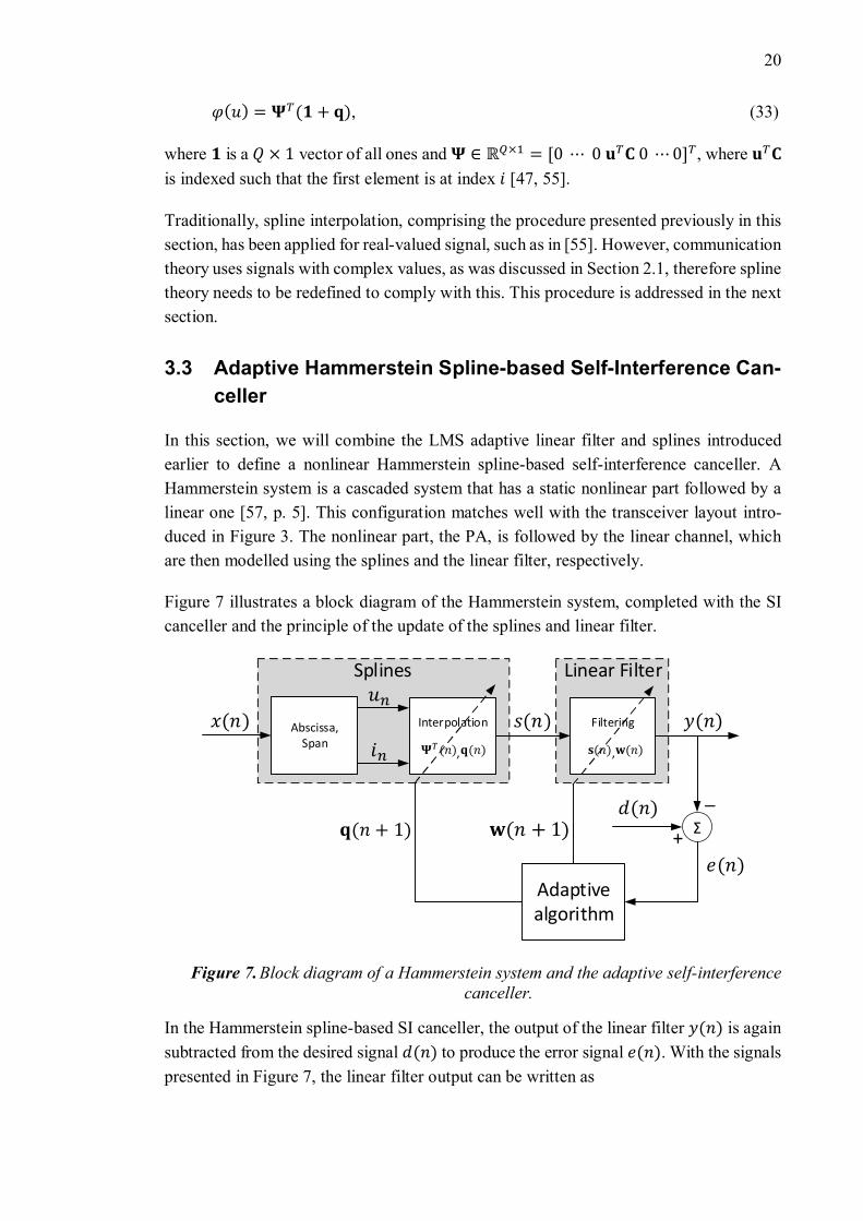
In this section, we will combine the LMS adaptive linear filter and splines introducedearlier to define a nonlinear Hammerstein spline-based self-interference canceller. AHammerstein system is a cascaded system that has a static nonlinear part followed by alinear one [57, p. 5]. This configuration matches well with the transceiver layout intro-duced in Figure 3. The nonlinear part, the PA, is followed by the linear channel, whichare then modelled using the splines and the linear filter, respectively.
Figure 7 illustrates a block diagram of the Hammerstein system, completed with the SIcanceller and the principle of the update of the splines and linear filter.
Splines Linear Filter
Abscissa,Span
Interpolation
( ) ( ),
Filtering
( ) ( ),
( )
Σ
_
+( )
( )
( )
Adaptivealgorithm
( + 1)( + 1)
( )
Figure 7. Block diagram of a Hammerstein system and the adaptive self-interferencecanceller.
In the Hammerstein spline-based SI canceller, the output of the linear filter ( ) is againsubtracted from the desired signal ( ) to produce the error signal ( ). With the signalspresented in Figure 7, the linear filter output can be written as

21
( ) = ( ) ( ), (34)
where ( ) is the impulse response of the linear filter at iteration and with memory ,
and ( ) ∈ ℂ × = ( + )… ( )… ( − ) , where and arethe filter pre-cursor and post-cursor taps, respectively [47]. Similarly to the adaptive lin-ear filter introduced in Section 3.1.1, the coefficients of the parts of the Hammersteinsystem have to be updated in order to achieve cancellation. The adaptive behavior is againbased on the information of the error signal ( ) = ( ) − ( ). In the system describedin Figure 7, the coefficients to be updated are the filter taps ( ) and the control pointsof the splines ( ). Thus, the cost function of the system can now be written in terms ofthe filter taps and the control points [54], considering only the instantaneous error:
( , ) = ∗( ) ( ). (35)
With the method of steepest descend, and by noting the decoupled nature of the system,the linear filter tap update algorithm can be written as
( + 1) = ( )+ ∗( ) ( ), (36)
where is the step-size for the filter and ( ) the regression of the splines output. Equa-tion (36) is equivalent to Equation (16), which was used to define an adaptive linear filter,with the exception of the input ( ) being replaced by the splines output ( ).
As mentioned in the previous section, the spline theory needs to be adapted for the use ofcomplex values. For this purpose, the following lines present the extension to complexspline interpolation from [47]. In this context, the index and abscissa values can be rede-fined by replacing ( ) with | ( )| in Equation (32) and removing in Equation (31),
as the absolute value makes the index value always positive. Additionally, Δ is definedas 1 for simplicity. Thus, the index and abscissa values can be expressed as
= ⌊| ( )|⌋+ 1 (37)
= | ( )| − ⌊| ( )|⌋. (38)
In order to model the complex behavior of the PA, two different real splines, modelingthe I- (real) and Q-branches (imaginary) are used. However, for the sake of simplicity thetwo splines can be combined in one single complex valued expression that contain bothof the branches. To this end, the interpolation scheme presented in Equation (33) is mul-tiplied by the input signal ( ) in order to retain its amplitude and phase and the controlpoints are redefined as complex values: = + . Hence, the splines nonlinearcomplex output can now be written as
( ) = ( ) ( )( + ( )). (39)

22
The update algorithm for the control points can be determined in a similar manner to thelinear filter. The method of steepest descend gives us:
( + 1) = ( ) − ( , ) (40)
( + 1) = ( ) − ∗( ) ( ) + ( )∗( ) (41)
( + 1) = ( )+ ∗( ) ( ) + ( ) +
( ) ( ) ∗+ ( ) ∗
, (42)
where is the step-size for the control points and ( ) is the output of the linear filter.The partial derivatives of the filter output can be defined as
( ) = ( ) ( ) ∗( ) (43)
( ) = ( ) ( ) ∗( ), (44)
where ( ) ∈ ℝ × = + … ( )… − is a matrix that collects past vectors ( ) as its columns and ( ) = diag ( + ),… , ( − ) is
a diagonal matrix containing past values of ( ). With Equations (43) and (44), thecontrol point update algorithm can be written as
( + 1) = ( )+ ( ) ( ) ∗( ) ( ). (45)
In conclusion, the Hammerstein spline-based canceller algorithm is a straightforward one.The splines output is first defined by Equation (39), after the abscissa and the span havebeen determined using Equations (37) and (38). Then, using the splines output, the linearfilter output is determined by Equation (34), and the error signal is defined with the out-put. With the error signal, the updates for the linear filter coefficients and spline controlpoints are applied after Equations (36) and (45), respectively [47].
The main merit of the Hammerstein spline-based canceller is its relative computationalsimplicity, compared to previous such algorithms [54], for example the memory polyno-mial model, introduced at the beginning of Chapter 3. This makes the spline-based modelconsume fewer resources when implemented on a given platform. The reduction of com-plexity is achieved without sacrificing performance much. Indeed, compared to thememory polynomial model, the reduction of complexity is 77 % in terms of multiplica-tions needed, with practically the same performance [47]. This reduction in complexityis important for implementing the canceller in resource scarce platforms and making thetechnology commercially feasible.

23
4. DEVELOPMENT ENVIRONMENT
In this chapter, we take a look at the development environment in which the self-interfer-ence canceller is built in. The digital SI canceller operates in the digital domain, whichwould make a computer an attractive platform. However, since the canceller should workin real-time, it cannot be implemented on a computer, but rather it is implemented on aField-Programmable Gate Array (FPGA) device. The FPGA is a chip that blurs the linebetween software and hardware, as the software that is programmed to be used on theFPGA, is actually physically wired within the chip. The FPGA in the implementation ofthis thesis lies inside a USRP, which is a software defined radio (SDR) device. In orderto give the FPGA the program, it obviously need to be written first. This part of the im-plementation is performed in LabVIEW Communications System Design Suite 2.0. Thecode written with LabVIEW contains other signal processing code necessary for the op-eration as well, but the focus in this thesis is on the SI canceller implementation.
4.1 USRP and FPGA
In this work, the hardware for the self-interference canceller is a Universal Software Ra-dio Peripheral. The Universal Software Radio Peripheral, or USRP for short, is a softwaredefined radio (SDR) device developed by Ettus Research, a brand of National Instru-ments. An SDR is a communications device, the operation of which can be programmat-ically controlled. This control over the functionality is what makes SDRs such versatileplatforms for communications engineering. If new functionality is to be added to a fullyanalog device, the whole system might have to be designed again. At least new physicalparts would have to be added to the system, which increases the complexity and costs ofthe device. In an SDR platform this is not an issue, since new functionality can be justprogrammed, and it will be implemented as part of the system. This greatly reduces thedeployment costs of the systems.
An SDR is not completely digital though. At least the RF frontend, which includes thetransceiver part of the system, is analog, in order for the signals to be transmitted andreceived. Between the analog and digital domains, the signal is converted accordinglyusing A/D and D/A converters (discussed in Section 2.2). In an USRP device, the frontendincludes direct-conversion transceivers for two channels. The digital signal processingpart outputs samples, that after the A/D conversion are transmit by the transmitter. Figure8 illustrates a high-level schematic of the USRP devices.

24
Figure 8. High-level schematic of a USRP device [45].
The digital signal processing in an USRP device is achieved with a Field-programmableGate Array (FPGA). An FPGA is a digital chip that can be configured to perform wantedcomputations. In many ways, the FPGA is similar to a microchip, as they both can beprogrammed and after doing so they both can act autonomously. Modern FPGAs consistof numerous generic logic blocks, which in turn consist of generic logic cells imple-mented on silicon using transistors. By giving the FPGA orders on how to connect thelogic cells and what kind of operation to perform on them, the functionality of the chip isdefined. This makes the signals inside the FPGA propagate in parallel, and thus the FPGAis an ideal device for real-time applications, which differentiates it from microchips.
In addition to the logic cells, FPGAs also include Digital Signal Processing (DSP) blocksand Block RAM blocks. DSPs are used for more complex arithmetic, for example multi-plications. Block RAM acts as internal memory for the device. The USRP contains aXilinx Kintex-7 model XC7K410T FPGA, the specifications of which are shown in Table1. The FPGA found in the USRP is compared to Kintex-7 model XC7325T, which canbe found in a National Instruments FlexRIO device PXIe-7972, which is also program-mable by LabVIEW.

25
Table 1. Comparison between the FPGAs found in an USRP and PXIe-7972 devices [64].
Element USRP PXIe-7972
Logic Cells 406 720 326 080
DSPs 1 540 840
Slices (4 LUTs & 8 flip-flops) 63 550 50 950
Block RAM (36Kb) 795 445
From Table 1 it can be seen that the FPGA found in USRP is superior in terms of resourcesto the one found in PXIe-7972 device. Especially crucial to the implementation are theDSP units, which are an important resource in digital signal processing. A memory poly-nomial self-interference canceller has been implemented on a PXIe-7972, and in that im-plementation the performance suffered from lack of available DSP units, described in[48]. Thus, the USRP offers a sufficient platform for the implementation of the self-in-terference canceller.
4.2 LabVIEW Communications System Design Suite 2.0
As crucial as the hardware for the implementation is its counter-part, the software. Thesoftware defines the behavior of the program by instructions on how to modify or transferdata. Although there are many alternatives, in this thesis the implementation of the self-interference algorithm is programmed with LabVIEW, more specifically with LabVIEWCommunications System Design Suite 2.0. LabVIEW (Laboratory Virtual Instrument En-gineering Workbench) is a visual programming language, developed by National Instru-ments. The LabVIEW language is based on a programming language called G, which isalso a visual language. LabVIEW is mainly aimed at data acquisition and visualization,although the applications of the language have expanded over the years. Nowadays, thereare numerous expansions and versions of LabVIEW, specifically tailored for certain typesof applications.
As stated previously, LabVIEW is a graphical programming language. This means thatthe programmer does not have to write the wanted functionality like in text-based lan-guages. In LabVIEW, all functionalities are defined as functional blocks, which aredragged and dropped on the coding platform. There are blocks for basic arithmetic, forexample addition and multiplication, and more advanced functionality as digital filtersand interfaces for hardware. Figure 9 illustrates a simple addition of two signed 32-bitinteger variables, realized in LabVIEW.

26
Figure 9. Addition of two variables in LabVIEW.
The code in Figure 9 can be realized in C++ as shown in Program 1.
In text-based programming languages, the code is executed row by row as seen fromProgram 1, and so it is easy to keep track of the order of the operations performed. How-ever, in LabVIEW the code is executed seemingly parallel (even though a CPU of a com-puter does the computation in series). In LabVIEW, a functional block is only executedwhen all data is available to it. This way, the user has more control over the flow of theprogram, yet with large programs, keeping track of the order of operations may becomecumbersome.
An advantage LabVIEW has over widely used text-based languages is that it provides theuser with a user interface (UI) without further programming needed. Indeed, two differentviews, the diagram, which defines the functionality, and the panel, which acts as the UIof the program, define a LabVIEW program. For example, for the code illustrated in Fig-ure 9, LabVIEW automatically creates two controls for the variables a and b and an indi-cator for the variable c. Using these, the user of the program could easily find out the sumof two integer numbers. This is unlike for example in C++, where achieving this level offunctionality would require substantial amount of code.
An important aspect of LabVIEW are the Virtual Instruments (VI), which act similarly tofunctions in text-based programming languages. The VIs can thus be used to simplify thedesigns, which in LabVIEW can quickly become hard to read. VIs, like functions in tra-ditional languages, make parts of the code reusable, since the same functionality can beachieved multiple times simply by calling the corresponding VI with the wanted func-tionality. This adds modularity to the programming tasks. The VIs are actually the partsof the program that hold both the front panel and the diagram that define the functionalityof the code. On a diagram, the VIs are presented by blocks, similar to any other part of
1234
int a;int b;
int c = a + b;
Program 1. Addition of two variables in C++.
27
the program. Controls and indicators determine the connections of the VIs, which act asinputs and outputs of the VI, respectively. The VI that is run when the execution of theprogram starts is called the top-level VI, and all the VIs the top-level VI calls are calledsubVIs.
LabVIEW Communications System Design Suite 2.0 is a standalone version of Lab-VIEW NXG, aimed specifically at communications engineering. The code written in Lab-VIEW Communications is the same as in regular LabVIEW, but the functional block havean emphasis on communications engineering, with such blocks as Wave Generation andFFT Spectrum. LabVIEW Communications also has FPGA tools incorporated within it.While it is possible to control the USRP with LabVIEW Communication without the needto program the FPGA separately, in this work the FPGA is also programmed. The wholeprogram is divided into two separate entities: the host code and target code. The host codecollects and sends data to the target code, visualizes the data, and controls the operationof the target code. These operations are carried out on a computer, since the USRP lacksuser-interface, and data visualization tasks are demanding and they do not need to beexecuted in real time. The target code is the code that is run on the FPGA of the USRP.The target code includes the transceiver code and the self-interference canceller. The tar-get code is also written as LabVIEW code but when it is finished, it is converted into abit file, which contains introductions for the FPGA on how to process the data. The bitfile is uploaded to the USRP’s FPGA when the host code is run.

28
5. IMPLEMENTATION
This chapter presents the implementation of the self-interference canceller in LabVIEWCommunications System Design Suite 2.0 in detail. The implementation, as discussed inChapter 4, is written in LabVIEW Communications version 2.0, and an USRP acts as thetarget device. Apart from the actual code, this chapter considers issues that rise from theselected hardware and software environment and solutions to those problems. These is-sues include the quantization, pipelining and complex number magnitude approximationon the FPGA. Additionally, this chapter focuses on the actual SI canceller implementationon the target FPGA, but naturally, the canceller is not independent of other code. Addi-tional code is required on the host side as well, to ensure the functionality of the SI can-celler and to control the behavior of it. The other bit of code consists mainly of transceiverrelated functionality, both on the FPGA and host side codes. An overview of the SI can-celler implementation on the FPGA is shown in Figure 10.
Read I/Qsamples
DigitalGain
Inter-polation
FrequencyShift
I/QImpairmentCorrection
Write I/O
Transmitter
Read I/OI/Q
ImpairmentCorrection
DecimationFrequencyShift
I/Q Datato Host
Receiver
Z-n
Decimation DiSICDC-offsetcancellation
60 MHz
Inter-polation
[ ]
[ ]
[ ]
120 MHz
Figure 10. Overview of the FPGA transceiver loop, complete with the SI can-celler.
Figure 10 shows that in addition to the actual canceller code, additional processing forthe signals is needed. The SI canceller code, even though computationally lighter thanprevious such algorithms, cannot be executed completely in one clock cycle of 8.33 ns,which corresponds to the native A/D data clock at 120 MHz. Therefore, the canceller

29
code is implemented in a 60 MHz loop, where the length of a clock cycle is 16.67 ns. Thechange of clock domain requires the input signals of the canceller to be decimated. Therelative clock speed is chosen to be half of the original sampling frequency, so that thedecimation operation is as easily implementable as possible. By choosing the SI cancellerclock domain to be 60 MHz, the decimation only requires to take every other sample ofthe signals from the 120 MHz loop. This is sufficient for the signal ( ) as it does notcontain any noise or other frequencies. Input ( ) needs to be properly decimated with adecimator, which includes a filter, to prevent aliasing. Conversely, the output of the can-celler, the signal ( ), needs to be interpolated with an interpolator back to 120 MHz. Inaddition to decimation, signal ( ) has to be delayed to correspond to the propagation ofthe signal in the circuitry and the registers of the program.
Even though the canceller operates at 60 MHz, which offers considerably more operationsto be executed in a single clock cycle compared to 120 MHz, not all of the required op-erations can be executed within one cycle. To get around this problem, the algorithm ispipelined. Pipelining is a programming method, where intermediate values of the algo-rithm are stored in internal registers of the device [36]. This way, the amount of operationsrequired to be performed in one cycle can be mitigated and controlled. In LabVIEW Com-munications 2.0, pipelining can be achieved by using feedforward blocks, illustrated inFigure 11.
Figure 11. Feedforward nodes in LabVIEW Communications 2.0.
The feedforward node shown in Figure 11 holds the input value until next cycle, and theinput is transferred to the output on the next cycle. The number on the node illustrateshow many clock cycles the value will be delayed by. The feedback node on the right inFigure 11 is functionally the same, except it has an additional enable input. When theenable input is asserted, the block functions the exact same as the normal feedforwardnode. When the enable input is false, the node retains the values in the registers untilenable is asserted again. This way, only valid data can be stored in the registers. Addingfeedforward nodes obviously adds delay to the system, so the amount of them should bekept to a minimum, for the system to retain real-time operation.
There are two separate major physical clocks used within the USRP. These clocks are theA/D converter clock, called Data Clock and the FPGA Clock, which runs at 40 MHz. Inorder to make use of the I/O nodes within the code, the code has to be clocked with theData Clock. Depending on the device, the Data Clock runs either at 120 MHz or at 200MHz. As mentioned previously, the canceller code is run at 60 MHz, which is half of the120 MHz that the used USRP runs the Data Clock at. However, it is only possible to

30
derive the 60 MHz clock from the FPGA Clock, which is not necessarily in synchroniza-tion with the Data Clock. Thus, the canceller code needs to be run slightly faster than halfof the Data Clock rate, 62 MHz in this work, in order to ensure that no data is droppedbetween the cycles. By doing so, the canceller loop will have non-valid values every nowand then. Therefore, the data will have a handshaking protocol on it, to tell the upstreamnodes whenever data is valid and can propagate forward in the code. The handshaking inthe canceller code is implemented using feedforward nodes with enable. Furthermore, toprevent false values from affecting the updates of and , the update only occurs whenthe first valid value has propagated through the algorithm, which in the implementationoccurs after seven clock cycles. This is achieved with the handshake protocol in the pro-gram, which propagates an ‘input valid’ signal throughout the code.
A major general challenge in the implementation is, in addition to the timing, the quanti-zation. As discussed in Section 2.2, in a digital environment the values of the algorithmare always of finite length, which gives rise to some problems. To ensure that the errorsfrom the quantizations are low, as many bits should be used for the values of the signalsas possible. There are limiting factors to this however, most notably the maximum bitwidths of the DSP blocks in the FPGA. A single DSP unit in a Kintex-7 device can handleat maximum values that are 18 and 25 bits long. In order to avoid overflowing and thususing unnecessarily many DSPs, the inputs of the multiplication operations should con-form to these bit widths. In addition to the DSPs limiting the bit widths, the maximum bitwidth that the FPGA can handle is 64 bits. The inputs are 16-bit signed integers, so theoutput should be the same type as well, which further restricts the possible values. Ma-nipulating the values within the code is achieved by using reinterpret and type cast nodes,illustrated in Figure 12.
Figure 12. Reinterpret, cast to fixed-point and cast to complex fixed-pointnodes in LabVIEW Communications 2.0.
The reinterpret node takes the bits that represents the input value and changes the inter-pretation of the value, without changing the bits. Thus, the input and output of the nodehave to have the same amount of bits. The casting nodes on the other hand take the valuethe input represents and change the type of value, so that, ideally, the value representedstays the same but the bits change. In the implementation, the cast nodes are mostly usedto limit the bit widths of the values. In these situations, the output value cannot entirelymatch the accuracy of the input, since the bit widths are smaller on the output. To mitigateerrors rising from this, the output values are rounded by using the half-to-even scheme.

31
Last general issue with LabVIEW in the implementation is the use of matrices. Eventhough LabVIEW Communications FPGA tools allow the use of two-dimensional matri-ces, these tools are cumbersome and difficult to use. The solution for this is to reduce thematrix operations of the SI canceller algorithm to corresponding 1-D array operations.This saves resources on the FPGA and gives more control for the user on the actual op-erations. It should be noted here, that in LabVIEW Communications array operations arealways element-wise.
5.1 Complex Number Magnitude Approximation
For the purposes of the implementation of the algorithm described in Section 3.3, theabsolute value or magnitude of a complex number has to be determined. The magnitudeof a complex number can be determined by the well known formula | | = √ + ,where is the real part, and is the imaginary part of the complex number. The issue ofthis computation is the demanding square root operation [42, p. 479]. On a computer, thisoperation is trivial, but on an FPGA or other resource scarce platforms, the operation hasto be simplified, since the standard way of defining the square root is by using iterativemethods, such as the Newton-Raphson algorithm [51]. Naturally, the reduction of thecomputation of the magnitude optimizes the performance even on platforms that haveresources to spare.
In this thesis, the magnitude of a complex number will be determined by using theαMax+βMin technique, described for example in [42, pp. 480—482] and [12]. As thename suggests, with this technique the magnitude of a complex number is approximatedby
| | ≈ ∙ max(| { }, { }|) + ∙ min(| { }, { }|), (46)
where and are constants. By using the αMax+βMin technique, the demanding squareroot operation is now reduced to mere multiplications and additions, which greatly re-duces the complexity of the computation compared to iterative algorithms. The techniquerequires the comparison of two real numbers, which is a straightforward operation, evenon resource scarce platforms. The constants are assigned values = 0.96043387 and= 0.397824735, which yield the least amount of error for an equiripple implementa-
tion, that utilizes only one value per constant [12]. These values yield an error for theapproximation that is less than 4 %. The difference between the actual magnitude and theαMax+βMin approximation of a complex number is illustrated in Figure 13.

32
Figure 13. The real magnitude and the αMax+βMin approximation of themagnitude of a normalized complex number.
Figure 13 shows the magnitude of a complex vector that has unity magnitude, which isillustrated in the figure as a constant line. The magnitude is plotted against the phase angleof the complex number, and the curve will repeat every 90°. The same unity magnitudevector’s magnitude is approximated with the αMax+βMin technique drawn in red. It canbe seen from Figure 13 that the error of the approximation is indeed within 4 % of theactual value of the magnitude. The mean absolute error of the αMax+βMin technique is2.4 % and the mean error is 1.3 % with the chosen parameter values. Therefore, the tech-nique is suitable for usage in the implementation.
5.2 Delay Estimation
In order to cancel the SI signal from the received signal, the input signals and of thecanceller have to have corresponding samples. This problem is trivial in a simulation en-vironment, where timing restriction do not apply. However, in a real life implementation,various parts of the program and circuitry, such as registers and A/D conversion, adddelay to the received signal. To cancel this effect, the transmitted signal has to be delayedaccordingly before the samples are fed to the canceller.
Determining a delay between two correlating signals is a straightforward process. Thecross-correlation of the signals tells about the similarity of two signals. Cross-correlationbetween discrete complex valued signals and is defined as
( ⋆ )( ) = ∗( ) ( + ) (47)
0 10 20 30 40 50 60 70 80 90Phase angle (°)
0.94
0.96
0.98
1
1.02
1.04
1.06Real magnitude
Max+ Min approximation

33
where denotes lag that is introduced to the signal and ∗ the complex conjugate of .In practice, cross-correlation means that the signal is delayed by one sample at a timeand the product between ∗ and is calculated every iteration. The more similar the twosignals, the higher the maximum value of the cross-correlation and the point of the max-imum value of the cross-correlation denotes the lag between the two signals [27].
5.3 Target Code
This section introduces the FPGA implementation of the SI canceller in more detail. The62 MHz loop, where the canceller is located is shown in Appendix A. In the cancellerloop, the signals ( ) (presented as ‘x[n]’) and ( ) (presented as ‘d[n]’) are read froma joined FIFO ‘DX_FIFO’, carrying unsigned 64-bit values. The 32 upper bits of theserepresent ( ) and lower 32 bits ( ). The joined values are immediately written to atarget-to-host FIFO ‘dx to host’. This FIFO is used on the host side to determine the delaybetween the signals and the DC-offset of the received signal. Before entering the cancel-ler, ( ) is delayed in a Discrete Delay block using the input ‘M1’, to correspond to thepretaps of the linear filter. Using the ‘Canceller on 60M?’ control, the user can controlwhether the samples propagate to the canceller or if the received signal is just immediatelytransferred back to the 120 MHz transceiver loop. The values are sent back using the‘E_FIFO’ FIFO. To validate the performance of the canceller, the same samples are alsosent to the host by using the ‘e to host’ FIFO.
The SI canceller is presented in Appendix A as the gray block with a wave and a redcross, within the case structure. The diagram of the SI canceller is illustrated in AppendixB. The operation of the canceller is divided into four distinct functional blocks for con-venience. The ‘Splines Estimation’ subVI calculates the spline interpolation of ( ) (‘xin’) and gives out ( ) (presented as ‘s[n]’), which is the input of the ‘Linear Filter’subVI. The linear filter determines the error signal ( ) and updates the filter coefficients.Finally, with the error signal, the spline control-points are updated in the ‘Splines Update’subVI.
The splines interpolation is the first operation that is performed on the signal ( ). Thesplines interpolation is achieved with the ‘Splines Estimation’ subVI, presented in Ap-pendix C. First, the single unsigned 32-bit value ‘x in’ representing signal ( ) is splitinto two 16-bit values, that are the I- and Q-branches of the signal. The branches are thenreinterpreted as <4.12> signed fixed-point values. The notation <4.12> denotes that thenumber’s presentation has 4 signed bits, in this case including the signed bit, and 12 frac-tional bits. This conversion is performed in order for the algorithm to use fixed-pointarithmetic and for the implementation to comply with the MATLAB model made of thealgorithm. The separate fixed-point values are then joined to make a single <4.12> com-plex fixed-point value.

34
In the top branch of the ‘Splines Estimation’ subVI, the absolute value or magnitude ofthe complex value ( ) is determined using the αMax+βMin method introduced in Equa-tion (46). The absolute values of the real and imaginary parts are determined and they arecompared with each other and multiplied accordingly. The magnitude of ( ) is thenused to determine and after (37) and (38), respectively. The value for is further usedto determine and a five element array of [ ] is created. This array will bethe input of the ‘Splines Row’ subVI. The ‘Splines Row’ subVI additionally takes as aninput. The output of the ‘Splines Row’ subVI is the new 11 element column for the splinesmatrix ( ). In order to save resources and reduce the complexity of the algorithm, therows are just delayed according to input ‘w_ind’, which will be explained later. This way,the rows are stored in registers instead of a matrix until they are needed for the calcula-tions. The other outputs of the ’Splines Row’ subVI are the three non-zero elements ofthe calculated row in an array. This array is fed to the lower branch of the subVI.
In the lower branch of the ‘Splines Estimation’ subVI the complex value of ( ) is storedas the first element of regressive array ‘x_n’, holding past values of ( ), the amount ofwhich is determined by the register ‘M’. The array ‘x_n’ represents the diagonal matrix( ) without the zeros. All computations in the implementation are adjusted accordingly.
The array is fixed sized, capable of holding 60 elements, but the apparent size is controlledby the register ‘M’, by adding zero values after index indicated by ‘M’. At the same time,the three values from the control-point array ‘q_i’ corresponding to are taken with the‘q subarray’ subVI. The subVI simply takes three consecutive values from the given ar-ray, starting from the given index. In LabVIEW, indexing starts from 0. After taking thecorresponding values, the splines output ( ) is determined after Equation (39). Thesplines output is cast as <5.13> type complex fixed-point value. The calculation is sim-plified by omitting the zero values from the ( ) array. Since the array multiplication iselement-wise, the resulting array’s elements are added up with a Sum Array Elementsblock. This result is finally multiplied with ( ) to produce the splines output ( ).
The calculation of the new spline matrix column in the ‘Splines Row’ subVI is presentedin Appendix D. The calculation of is performed in this subVI. From Equations (29)and (30) it follows that is defined as
= [ 1]1 −2 1
−2 2 01 1 0
= − + − + + . (48)
The first operation in the subVI is multiplication of the five element array ‘u array’, whichis described above, and a constant array corresponding to the non-zero values of matrix
. The output of the multiplication is a five element array (− ) (− ) ( ) .
These elements are then taken accordingly to create a three element described in Equation(48). This three-element array is the ‘splines reduced’ output. For the ‘splines row’ output,

35
the array is inserted into an 11-element array of zeros at index determined by , thuscreating the vector ( ), which is the new column for matrix ( ) as well.
On the FPGA, all array lengths have to be fixed. This is why the FPGA code does notsupport the Array Subset functional block, as the output array can have varying sizes.Instead, taking a subarray has to be implemented as seen in ‘q subarray’ subVI in Appen-dix E. In the ‘q subarray’ subVI, three elements from the array are taken separately,starting from the input ‘index’. After the elements have been taken, they are used to forma three-element array, which acts as the output ‘subarray’. With this approach, even if theinput ‘index’ exceeds the length of the input array ‘q’, the returned elements are just ze-roes, and the output array has a fixed length of three. This is unlike using the Array Subsetblock, which would return an array with less elements.
After the ‘Splines Estimation’ subVI, the splines output ( ) propagates to the subVI‘Linear Filter’. The subVI applies the linear filtering to the signal, and updates the filtertaps. This subVI is illustrated in Appendix F. First, the signal ( ) is placed in a regres-sional array ( ), indicated by ‘s_n’. Again, the array has a fixed length of 60 elements,but the apparent size can be altered with the register ‘M’, similarly to the ‘x_n’ array in‘Splines Estimation’ subVI. The array ‘s_n’ is then multiplied with the conjugate of filtertaps array ‘w_n’ according to Equation (34), to produce the model output signal ( ). Toproduce this product, the complex conjugate of every element in the filter tap is taken,and the element-wise products are added together to produce a single value. The summa-tion of the element-wise product array elements is achieved with the ‘Sum Array Ele-ments’ subVI. The output ( ) is then subtracted from the desired signal ( ) to producethe error signal ( ). Before this, the DC components of both I- and Q-branches are can-celled by a simple subtraction. The signal ( ) (presented as ‘d in’) is, similarly to ( ),interpreted as signed <4.12> complex fixed-point number. After the error signal is deter-mined, in the top branch it is fed as is to the output ‘e(fxp) out’. Below this, the fullaccuracy error signal is cast as signed <4.12> complex fixed-point value. This value isfurther split into its real and imaginary parts, which in turn are reinterpreted as signed 16-bit numbers, to follow the number representations of the inputs. Finally, the separatebranches are joined to form a single unsigned 32-bit value, where the high bits representthe imaginary (Q) part and low bits the real (I) part of the error signal.
The update of the filter taps is performed as described in Equation (36). The fully accurateerror signal is first conjugated and bit shifted according to the input ‘mu_w’. By substi-tuting the multiplication ∗( ) with a bit shift, DSPs are saved for other operations.After this, the remaining calculations for the update are performed, with multiplication of
∗( ) with the corresponding array , indicated again by ‘s_n’, and finally adding theresult to ( ), indicated by ‘w_n’. The result is applied to the register ‘w_n’ only whenthe inputs ‘update w?’ and ‘input valid’ are asserted. If the user so desires, the update ofthe filter coefficients may be stopped with the ‘update w?’ control, which is set in the host
36
code. Furthermore, it is possible to reset the array of ( ) by writing true to the ‘reset qand w’ register, which is read within the case structure where update of ( ) is applied.
In order to determine the product of ( ) ( ), the elements from the element-wisemultiplication have to be added together. This operation is performed in the ‘Sum ArrayElements’ subVI, shown in Appendix G. LabVIEW provides the user with a built-in func-tion that sums the array elements together, which is also utilized in the ‘Sum Array Ele-ments’ subVI. The issue with using this functional block to determine the sum of the arrayelements at once is that it provides overhead, and the operation cannot be scheduled forlarger arrays, even at relatively low frequencies. Thus, in order to be able to use the full60 elements of the ( ) and ( ) arrays, the summation is divided into 12 parallel sumsof five element subarrays. Here, the Array Subset functional block may be utilized, as thestarting indices of the subarrays are fixed. The sums of the subarrays are then added to-gether, to determine the total sum of the elements of the array, thus producing( ) ( ).
After the error signal is determined in the linear filter, the signal is used to update thespline control points in the ‘Splines Update’ subVI. In addition to the error signal, the‘Splines Update’ subVI takes the current value of ( ), indicated as ‘w_n in’, as an inputfrom the ‘Linear Filter’ subVI, and ( ) and ( ), indicated respectively as ‘q_i in’ andX in, from the ‘Splines Estimation’ subVI. The ‘Splines Update’ subVI is illustrated inAppendix H. The update of the control points is determined in accordance to Equation(45). In the implementation, the calculation of matrix multiplication ( ) ∗( ) ( ) issimplified by only considering five most significant taps of the filter. The most significanttaps are usually around the + 1 tap [47], so the first the taps − 1, , +1, + 2 and + 3 are taken from the ( ) array with the ‘w subarray’ subVI.The subVI is similar to ‘q subarray’ but instead of two consecutive values of the indexinput, five consecutive values are taken instead to form a five element array. The corre-sponding values are taken from the ( ) array similarly with the ‘X subarray’ subVI. Thevalues to be taken are determined by the input ‘w_ind’. Similarly to the control ‘M1’ inthe canceller loop, ‘w_ind’ is controllable from the host, and it is determined to be −1. Therefore, the five element subarrays from and the array ‘x in’ correspond to thewanted values near the most significant tap. The subarray of ‘x in’ is conjugated andmultiplied with the subarray of ‘w_n’ to produce a reduced version of ∗( ) ( ), withonly five elements. The product is further multiplied with ( ) in ‘Splines x X*w’ subVIto finally produce ( ) ∗( ) ( ). Meanwhile, the error signal is bit shifted the same asin the ‘Linear Filter’ subVI to produce ( ), instead of multiplying it with in orderto save DSPs. The remaining steps of the update are applied by multiplying( ) ∗( ) ( ) with ( ), the product of which is then added to the current values of
the control points. Similarly to the filter tap update in ‘Linear Filter’ subVI, the update ofthe control points is controlled by ‘update q?’ input, which is asserted from the host code.Additionally, the ’input valid’ input has to be asserted for the update to take place. It is

37
also possible to reset the control points with the ‘reset q and w’ register, the same as withthe filter taps.
The calculation of ( ) ∗( ) ( ) is performed in the subVI ‘Splines x X*w’ is pre-sented in Appendix I. The calculation can be simplified as stated earlier, if only valuesnear the most significant tap are taken into account. This is why it is sufficient to keeptrack of five columns of the matrix ( ). The columns of the spline matrix ( ) areregressional, which means that a new column calculated in the ‘Splines Estimation’ subVIwill be the new first column of the matrix, while the last column will be discarded. Thenew column is of no interest immediately however and thus it is delayed in the ‘SplinesEstimation’ subVI, until it corresponds to the five columns near the most significant tapof the filter. The columns of the spline matrix are stored in registers ‘splines_1’ through‘splines_5’ and the columns are regressed by writing the array from the register to thenext after it is read. The reduced calculation of ( ) ∗( ) ( ) can be written as:
⎣⎢⎢⎢⎡ ,
,
, ,
,
,
, ,
,
,
,⋮,
,
,
, ,
,
,
, , ⎦
⎥⎥⎥⎤
⎣⎢⎢⎢⎡
⎦⎥⎥⎥⎤= (49)
⎣⎢⎢⎢⎡ , + , + , + , + ,
, + , + , + , + ,
, + , + , + , + ,⋮
, + , + , + , + , ⎦⎥⎥⎥⎤
, (50)
where represents the elements in the spline matrix ( ), and the elements in thereduced array ∗( ) ( ). Since only the columns of the spline matrix are stored in reg-isters, the rows have to be formed with the build array blocks within the subVI. The fiveelement rows are then multiplied element-wise with the reduced ∗( ) ( ) array. Theelements of the resulting array are then summed together, to form the eleven elements ofthe resulting array in (50). In the final step, the elements are built into an array that ispassed as the output of the subVI.
The Hammerstein spline-based SI canceller is a low complexity approach to the SI can-cellation problem. The reduced complexity is highlighted mainly in the comparativelylow number of DSP units required for the implementation. The resource utilization of thealgorithm implementation is shown in Table 2.

38
Table 2. Resource usage of the SI canceller on the FPGA.
Element Total Used Percentage (%)
Registers 508 440 37 778 7.3
DSPs 1 540 533 34.6
Block RAM 795 3 0.4
LUTs 254 200 67 632 26.6
Total Slices 63 550 22 183 34.9
Table 2 shows that with 60 taps of memory in the linear filter, the implementation usesonly 34.6 % of the available DSP. This value could be easily reduced for more resourcescarce platforms, as the performance of the canceller does not greatly decline even withreduced memory. Additionally, the amount of LUTs, which handle the logic operationson the FPGA, is at acceptable levels with only 26.6 % of the available ones used by thealgorithm. Even though the implementation utilizes the pipeline technique and valuessuch as the spline matrix row, linear filter taps and spline control points are stored inregister, the register usage of the algorithm is merely 7.3 %.
5.4 Host Code
The host code running on a desktop computer provides the user-interface of the FPGAprogram, since the USRP does not provide direct interaction with the user. The purposeof the host code is to control the program on the FPGA and visualize measured data thatis transferred to the computer. The control and visualization of the transceiver code andrelated data is omitted here, and the focus is on the SI canceller. Most of the variablesmentioned in Section 5.3 are assigned values with the Write FPGA Control functionalblock, which as the name suggests, writes values to the control values of the FPGA VI.This is unlike regular LabVIEW, where instead of controls, the variables have to be as-signed using other means. The controllable values are shown in Appendix J, along withthe user-interface of the program. The left side of the UI is dedicated to controlling thetransceiver and visualizing data read from the FPGA, while the right side controls the SIcanceller. The visualized data includes a spectrum and a received power plot. Thememory, pretaps and the learning rates of the SI canceller can be assigned values to theusers liking, but in order to ensure the best performance of the canceller, the delay be-tween transmit and received signals need to be known exactly. Furthermore, the DC-off-set of the received signal needs to be mitigated. These issues are handled in a host codeloop, illustrated in Appendix K. The delay between the transmit and received signal isdetermined by using the cross-correlation, introduced in Equation (47). The length of the

39
read signals is subtracted from index of the maximum value, which gives the delay be-tween the two signals. The user then changes the ‘x Delay’ control, until the delay isshown to be zero. The DC-offset of the received signal is determined simply by deter-mining the mean of the signal. In order to avoid abrupt changes, the previous values affectthe measured DC-offset according to
( + 1) = ( )+ (1 − ) ,̅ (51)
where is the determined DC-offset, is a value between 0.9 and 0.99, and ̅is themean of the received signal. Value of 0.95 is chosen for in this implementation. Themean of the received signal is determined from a set of 65536 samples. This is the depthof the FIFO, which transfers the data between the FPGA and the host PC. The DC-offsetis determined separately for the real (I) and imaginary (Q) parts of the signal. As opposedto the delay correction of the signal ( ), the measured DC-offset values are written tothe FPGA every cycle of the loop automatically.

40
6. EXPERIMENTS AND RESULTS
The functionality of the self-interference canceller implementation introduced in the pre-vious chapter is validated with measurements in this chapter. The verification of the per-formance is divided into two main parts: functional validation, which validates the SIcancellation capabilities of the canceller in three scenarios, and full-duplex operation,which studies the system’s ability to function in an actual full-duplex communicationscenario. As mentioned previously in Section 2.3, in order to achieve sufficient cancella-tion of the SI for the full-duplex system to be feasible, both analog and digital cancellationmethods have to be utilized. In the measurements, the digital canceller is fixed as the onedescribed in the previous chapter, running on USRP-2953R devices’ FPGAs. The analogcancellation is achieved by two different methods: two separate antennas and an RF can-celler, which also incorporates a circulator, allowing the use of a single antenna. The twosetups are presented in Figure 14.
Figure 14. The two setups used in the measurements: the two-antenna node(left) the RF canceller node (right).
The two-antenna setup achieves the analog cancellation of the SI by adding isolation be-tween the transmitter and receiver chains. In the setup, the isolation is approximately 33dB. The antennas are commercial off-the-shelf monopole antennas designed for 2.4 GHzISM band. In the RF canceller setup, the analog cancellation is achieved with the analogRF canceller. The RF canceller is an adaptive one, and it is controlled with a laptop. Likethe digital canceller, the RF canceller estimates the effects of the channel and nonlinear-ities, and subtracts the estimate of the SI signal in a combiner. The RF canceller has threetaps of memory. The RF canceller is connected to a circulator, which in turn is connectedto a designated custom dipole antenna, which is also designed for 2.4 GHz ISM band.The RF canceller is capable of suppressing the SI signal by up to 48 dB, and in addition,the use of circulator adds around 20 dB isolation between the transmission and receptionchains, making the maximum amount of total achievable isolation in the order of 70 dB[59].

41
6.1 Signal-to-interference-plus-noise Ratio, Symbol Error Rateand Sum Rate
For the purposes of analyzing the performance of the full-duplex system, three figures ofmerit are introduced. These figures are the signal-to-interference-plus-noise ratio (SINR),symbol error rate (SER) and channel capacity. In order to utilize the metrics, the signalhas to carry symbols as its payload. To this end, QAM-signals are used. An -QAM cancarry different symbols, which make up the alphabet of that particular QAM-signal.The symbols in the alphabet represent ( ) bit binary numbers. The alphabet can bepresented in a constellation, which a presentation of the symbols in Cartesian coordinates.The coordinates are translated into complex values, which allows the use of I/Q-modula-tion for the symbols [65, pp. 447—481]. For example, in a 16-QAM signal, the alphabetholds 16 different symbols, and the symbols are 4 bit long. Furthermore, the constellationhas 16 points, all of which are assigned a different symbol they represent. An example ofa 16-QAM signals alphabet is presented in Figure 15, with possible assigned symbolsshown on top of the points.
Figure 15. Constellation of a 16-QAM alphabet, with the symbols shown.
SINR can be estimated by the magnitude of the error of the received symbols comparedto the ideal ones. Ideally, the samples sent by the transmitter would be received on thereceiver side with only channel effects on the samples. However, the received signal alsoincludes noise and interference [66], and the samples are distorted even further. Since thesystem usually transmits and receives more than one symbol, the SINR can be defined asthe average of the deviations from the ideal values. An estimate of the SINR in decibelscan be therefore be formally written as
SINR = 10∑ ,
∑ , , (dB), (52)
-1.5 -1 -0.5 0 0.5 1 1.5In-phase component
-1.5
-1
-0.5
0
0.5
1
1.5
0000 0001 0010 0011
0100 0101 0110 0111
1000 1001 1010 1011
1100 1101 1110 1111
Model symbol

42
where is the amount of symbols sent and received, , the ideal symbol at index , ,
the received symbol at index and ℎ the channel estimate for the th symbol. It shouldbe noted, that the SINR figure is indeed an estimate, as the calculation of it relies ondetermining the channel response, which in itself is an approximation. The channel canbe estimated using the received and transmit signals, using for example the least squaresmethod, which gives more accurate results than LMS. Assuming the channel model isadequate, , ℎ presents the received symbols without any interference or noise. Sincethese effects are inevitably contained within the real received signal, determining , ℎ −
, only leaves the interference and noise, assuming these are the only distorting factorsin the system. Higher values for SINR denote better performance, as the magnitude of theerror induced by interference and noise gets smaller.
Figure 16. Constellation of potential received symbols, supposed to representsymbol 1001 in Figure 15.
SER is a measure of the frequency of errors in the constellation of the received symbols.An error in the constellation occurs when a received symbol is misinterpreted. The inter-pretation of the symbols can be achieved simply by dividing the constellation intosquares, centered at the ideal symbols. Now, if the received symbol is not located withinthe square of the intended symbol, the received symbol is interpreted incorrectly, whilesymbols within the intended square are correctly interpreted [65, pp. 447—481]. SER canbe defined as the portion of the deficits compared to the total number of symbols received.Formally, it can be expressed as:
SER = , (53)
-1.5 -1 -0.5 0 0.5 1 1.5In-phase component
-1.5
-1
-0.5
0
0.5
1
1.5Model symbolCorrectly interpreted symbolIncorrectly interpreted symbol

43
where is the amount of misinterpreted symbols. Figure 16 illustrates a constellation offive possible symbols being interpreted in the alphabet introduced in Figure 15. Suppos-edly, all of the received symbols should represent the symbol 1001, but only the symbolsmarked as green squares achieve this, while the red crosses are misinterpreted. Assumingonly these five symbols were transmit, the SER of this particular system would be 0.60,since, out of five symbols, three were misinterpreted.
Finally, the channel capacity for a single node can be determined with Shannon’s ca-pacity theorem [16, p. 100]:
= 1 + 10( )
(bits/s/Hz), (54)
where SINR(dB) is the measured SINR figure of the node in decibels. The capacity pre-sented in (54) is normalized, as it does not take into account the bandwidth of the system.Considering only two nodes with capacities and in the system and assuming thetwo devices transmit exactly half of the time, the sum rate or the total capacity in half-duplex operation, , can be determined as = ( + ). Similarly, assuming that
both nodes transmit constantly in full-duplex operation, the sum rate in this scenario canbe written as = + , where is the total capacity in full-duplex operation.
6.2 Functional Validation
The aim of the functional validation test is to validate that the digital canceller is capableof cancelling the SI from the received signal. To this end, the digital canceller is measuredin two distinct scenarios, first being the two-antenna node and the other the RF cancellernode, introduced earlier. The measurements with the two-antenna node and the RF can-celler fully utilized are actual operation environments for the canceller, and thus displaythe performance of the implemented algorithm. The experiments were conducted in alaboratory environment, by placing the node under test in the center of the room, in orderto minimize reflections from other objects. The recorded data consists of the receivedsignal right before the digital canceller and the error signal just after the canceller, asillustrated in Appendix A. The measurements were conducted in 2.4 GHz frequency using10 different transmitter (TX) powers, from 0 dBm to 18 dBm in intervals of 2 dBm. Thesignals used are 10 MHz bandwidth random OFDM signals, and they are frequencyshifted to a digital intermediate frequency (IF) of −15 MHz. The payload consists of 16-QAM symbols.

44
Figure 17. Power spectral densities in four measurement cases: Two-antennanode with 8 dBm TX power (top left) and 16 dBm TX power (top right), and RFcanceller node with 8 dBm TX power (bottom left) and 16 dBm TX power (bot-
tom right).
Four power spectral densities of the measurements are shown in Figure 17, with twotransmit powers (8 dBm and 16 dBm) for both of the nodes. The plots illustrate the trans-mit signal of the node, the received signal before the digital cancellation, the signal afterthe cancellation stage, and the device noise floor for reference. The spectra in Figure 17show that the digital canceller is capable of providing further cancellation to the SI signalin addition to the analog cancellation. Moreover, the measurements with 16 dBm transmitpower illustrate that the canceller indeed suppresses the nonlinearities of the receivedsignal. This further improves the overall inband cancellation result. Since the RF cancelleris capable of cancelling the nonlinear effects of the received signal as well, the cancella-tion of the nonlinearities in the RF canceller node with 16 dBm transmit power is lessimpressive. Still, the digital canceller is able to provide additional cancellation on top ofthe analog one, reducing the residual power of the SI canceller close to the noise floor. Inthe two-antenna node, the residual inband power is still approximately 17 dB over thenoise floor, yet the inband cancellation of the SI signal is around an impressive 45 dB. Inthe case of 8 dBm transmit power, the residual power is reduced close to the noise floor
PS
D [d
Bm
/MH
z]
PS
D [d
Bm
/MH
z]
PS
D [d
Bm
/MH
z]
PS
D [d
Bm
/MH
z]

45
on both of the nodes, with the RF canceller node being less than 1 dB away. This is dueto the initial power of the SI being relatively low and having little nonlinear distortion.These results indicate that with enough analog suppression of the SI, the system is ableto almost fully cancel out the SI signal with the digital canceller, even in the presence ofsevere nonlinear distortion.
Figure 18. Inband cancellation of the SI signal with different transmit powersin both measurement cases.
The inband cancellations with different transmit powers in both measurement scenariosare presented in Figure 18. The difference between the cancellations provided by the dig-ital canceller in the two nodes is a consequence of the RF canceller providing more iso-lation between the transmitter and receiver chains than the two-antenna node. The twoantennas provide a fixed isolation of around 33 dB in all of the measurement cases,whereas the isolation of the RF canceller fluctuates between 62 dB and 68 dB in themeasurements. This is due to the RF canceller being an active device, adapting to eventhe smallest changes in its surroundings. As mentioned previously, the residual power ofthe SI is close to the device noise floor in the RF node, which limits the achievable inbandcancellations. In fact, the achieved digital cancellation of the SI is limited by the devicenoise floor, since it is physically impossible to push it below this limit. Additionally, theperformance if the canceller is hindered by the application of the αMax+βMin technique,which only approximates the magnitude of the input signal. With the received power rel-atively high in the two-antenna scenario, the digital canceller still has a lot of power tocancel, even after analog suppression. This is why the inband cancellation in the two-antenna scenario lies between 40 dB and 50 dB, with the peak cancellation being around48 dB achieved with 10 and 12 dBm transmit powers. This level of cancellation exceedssimilar real-time realizations, described for example in [5] and [33], where the reporteddigital cancellations are 43 dB and up to 35 dB, respectively. More recently, [19] and [35]have utilized machine learning and neural networks, respectively, to obtain digital can-cellations of 50 dB and 45 dB, respectively. Thus, the implemented digital canceller in
46
this work is among the state-of-the-art solutions in the field, in terms of achieved cancel-lation.
Considering the antennas produce around 33 dB of isolation between the chains, the max-imum combined suppression of the SI in the node is in the order of 80 dB. With transmitpowers less than 6 dBm, the SI canceller is able to reduce the residual power level of theSI signal to within 2 dB of the device noise floor. Both of the cancellation results riseuntil the optimal operation point is achieved at 12 dBm, after which the cancellation re-sults start to decline due to increasing nonlinearity of the system. It should be noted thatwith the two-antenna measurements, there is always some low amount on residual SI lefton the cancelled signal. In the RF canceller scenario, the inband cancellation of the digitalcanceller remains low compared to the antenna node measurements, but that is due to thecombined cancellation reaching the noise floor with negligible difference. The noise flooris reached with the RF canceller node with transmit powers up to and including 8 dBm,after which the residual power is around 1 to 2 dB from the noise floor. With 18 dBmtransmit power, the difference goes up to around 5 dB. The maximum achieved digitalcancellation with the RF node is around 22 dB with 10 dBm transmit power, and with 14dBm transmit power, the node is capable of providing total isolation of up to 90 dB. Thisfigure combines the 68 dB of isolation the combination of the RF canceller and the circu-lator provides, and digital cancellation of 21 dB of the digital canceller.
6.3 Bidirectional Full-duplex Operation
In order to illustrate the communication capabilities of the implemented canceller, theutilized nodes were used in a communication link. The measurements consider the re-ceived signal from the opposing node in half-duplex (HD) and full-duplex (FD) scenarios,and the quality of the link is determined by the figures of merit introduced in Section 6.1.The measurements were carried out again in a laboratory environment to ensure the leastamount of interference from external sources. The measurements were conducted with acenter frequency of 2.4 GHz. The transmit signals were random OFDM signals with abandwidth of 20 MHz and 64-QAM symbols as the payload. The utilized transmit powersare the same as in the functional validation measurements: from 0 to 18 dBm with inter-vals of 2 dBm. Two sets of measurements were carried out, one with the nodes in thesame room, and another with a wall separating the nodes. This will give evidence that thecanceller is capable of operating in various circumstances. The measurement case with aline-of-sight between the nodes acts as a proof-of-concept measurement, whereas the casewhere the line-of-sight is obstructed by a wall resembles more an actual communicationsscenario. In both cases, the separation of the nodes was 4 meters.

47
6.3.1 Line-of-sight case
Figure 19 illustrates the SINR and SER results of the two nodes with the nodes in thesame room. The SER result is presented in a semi-logarithmic plot, as the obtained valueshave a large range. For the cases with no misinterpretations in the symbols, the SER isassigned value 2.2204 ∙ 10 , which is the used spacing between double precisionsnumbers in MATLAB. All results are an average of around 20 measurements, in order tominimize the effects of random variation.
Figure 19. SINR and SER of both nodes in half-duplex and full-duplex scenar-ios, with different transmit powers, the nodes in the same room.
Overall, the results in Figure 19 show that the employment of the FD scheme has negativeeffects on the quality of the received signal. Since the nodes are not similar and the othernode includes two antennas, the setup and the environment are not symmetrical for thenodes. Hence, it is more sensible to compare the HD and FD operations within the samenode, as opposed to comparing all of the performances together. Both nodes showcasesmaller differences in the SINR results between the respective HD and FD cases in lowertransmit powers, which is reasonable, as the residual power of the SI after digital cancel-lation is close to noise floor in these cases. Higher transmit powers leave more power ofthe SI on the received signal, and thus the SINR difference rises up to around 4 dB intransmit powers between 10 and 14 dBm. With transmit powers even higher than these,the nonlinear distortion is heavy in both HD and FD cases, which deteriorates both per-formances. From all of the results, it can be seen that the SINR rises until 12 or 14 dBm
SIN
R [d
B]
SER

48
after which it starts to drop, due to nonlinear behavior of the transmitters. The SER resultsare especially sensitive to random variations in the data as results are low, hence the SERcurves do not display as clear curves as the SINR results in Figure 19. Still, higher SINRresults generally denote better SER results as well, and thus the SER results are at theirlowest when the SINR results are at their highest. The SER results show that only thetwo-antenna node is capable of interpreting the symbols perfectly with transmit powersof 12 and 14 dBm, while the other cases have misinterpretations with all powers. As isthe case in with the SINR, the difference between the SER results in respective HD andFD cases are lower with low transmit powers, with the SERs of the RF canceller beingnearly identical. The gap again rises with powers between 10 and 16 dBm, while the 18dBm cases exhibit again less difference between the HD and FD cases. All of the casesexhibit relatively low SER values, however, which suggests the link is capable of trans-ferring most of the information to the receiving node intact. The SINR and SER resultscombined demonstrate that with the adequate operating conditions, the information canbe conveyed successfully in a bidirectional FD scenario, with acceptable decline in per-formance. Furthermore, practical communications systems utilize channel coding that cancorrect misinterpreted symbols, thus mitigating the need to transfer all data intact. Indeed,in a practical communications system resources are wasted if the SER of the uncodedsignal drops to zero, which is not a desired feature. Thus, reaching SER values of zero isnot necessary for the documented system to be a viable option for an actual communica-tion implementation.
Figure 20. Constellations of the received symbols in the two-antenna node, inHD (left) and in FD (right) operations with 12 dBm TX power, both nodes in the
same room.
Figure 20 illustrates the difference between the HD and FD operations in terms of theconstellations. The exhibited case is where the difference between the schemes is at itshighest, in the two-antenna node with 12 dBm transmit power. Clearly, the FD schemeadds noise to the received signal, which was also seen in the SINR results in Figure 19.
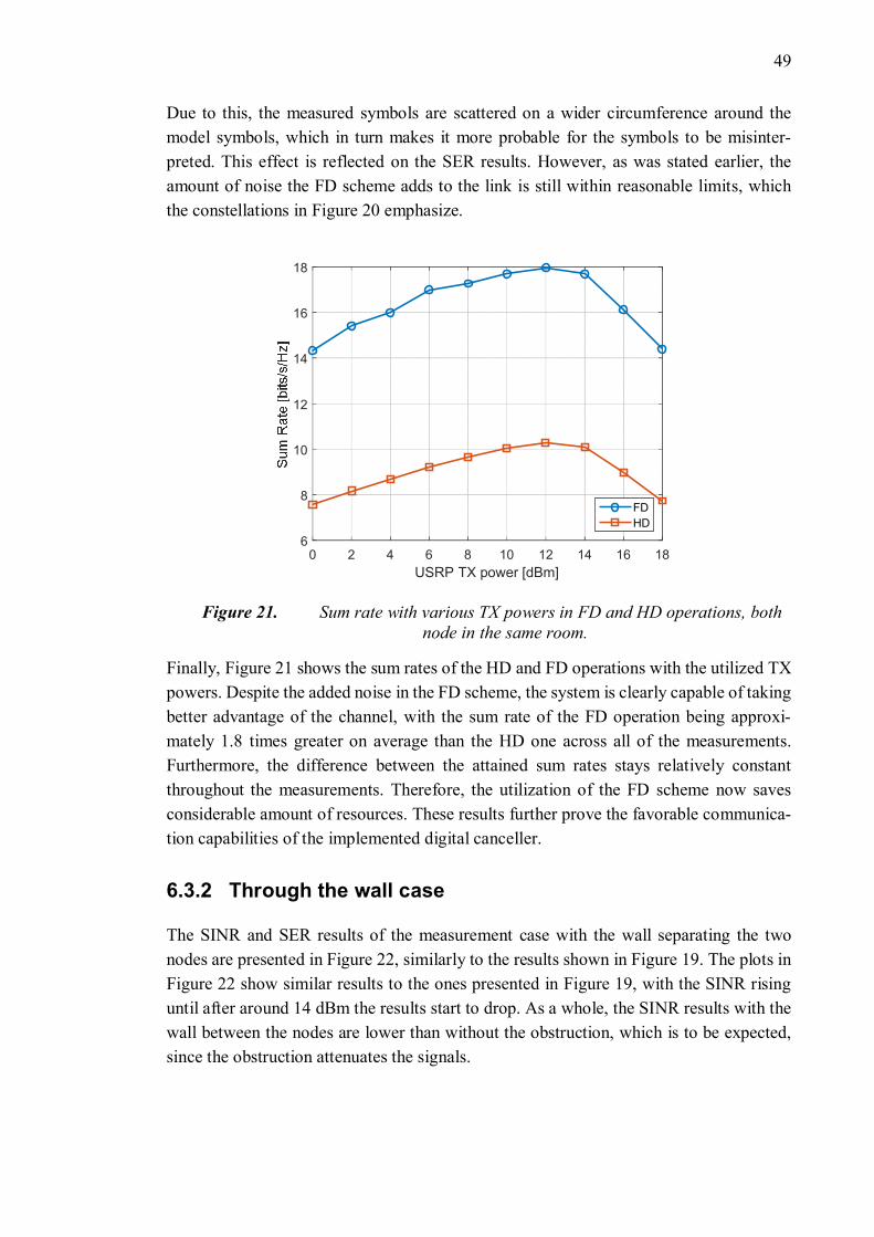
49
Due to this, the measured symbols are scattered on a wider circumference around themodel symbols, which in turn makes it more probable for the symbols to be misinter-preted. This effect is reflected on the SER results. However, as was stated earlier, theamount of noise the FD scheme adds to the link is still within reasonable limits, whichthe constellations in Figure 20 emphasize.
Figure 21. Sum rate with various TX powers in FD and HD operations, bothnode in the same room.
Finally, Figure 21 shows the sum rates of the HD and FD operations with the utilized TXpowers. Despite the added noise in the FD scheme, the system is clearly capable of takingbetter advantage of the channel, with the sum rate of the FD operation being approxi-mately 1.8 times greater on average than the HD one across all of the measurements.Furthermore, the difference between the attained sum rates stays relatively constantthroughout the measurements. Therefore, the utilization of the FD scheme now savesconsiderable amount of resources. These results further prove the favorable communica-tion capabilities of the implemented digital canceller.
6.3.2 Through the wall case
The SINR and SER results of the measurement case with the wall separating the twonodes are presented in Figure 22, similarly to the results shown in Figure 19. The plots inFigure 22 show similar results to the ones presented in Figure 19, with the SINR risinguntil after around 14 dBm the results start to drop. As a whole, the SINR results with thewall between the nodes are lower than without the obstruction, which is to be expected,since the obstruction attenuates the signals.
0 2 4 6 8 10 12 14 16 18USRP TX power [dBm]
6
8
10
12
14
16
18
FDHD

50
Figure 22. SINR and SER of both nodes in half-duplex and full-duplex scenar-ios, with different transmit powers, the nodes separated by a wall.
Again, it is most reasonable to compare the SINRs within one node, as the environmentis not symmetrical. Similarly to the previous case, the SINR results are closer to eachother in both nodes with lower transmit powers, but with optimal powers, the differencegrows significantly. This effect is also present in the previous case, but not as nearly asdistinctly as in this one. The SINR difference between HD and FD schemes is around 2dB in the two-antenna node with powers less than 8 dBm and afterwards the differencerises up to some 6 dB at 14 dBm transmit power. The difference is less than 1 dB in theRF canceller node with low powers, and only rises up to around 4 dB at 14 dBm transmitpower. These results are reflected in the SER plot, with all SER results being practicallysame at low transmit powers. The difference between HD and FD schemes is nearly iden-tical to the previous test case, with the exception that all results have dropped by an orderof magnitude. With higher powers, the SER results in HD cases drop, but before that, theresults do not differ greatly from each other. In this case, none of the measurement resultsdemonstrate perfect interpretation, as the SER never drops to zero, but, as was statedearlier, that is not an issue. These results indicate that the wall has an effect on the receivedsignal quality, and the proximity of an obstacle reduces the functionality of the SI cancel-ler, thus deteriorating the FD operation. Still, the link is able to convey messages over it,with acceptable degrading of the performance, as was the case in the first measurementscenario. Conclusively, the SI canceller is capable of suppressing the SI signal in a man-ner, which does not excessively interfere with the communication link.
SIN
R [d
B]
SE
R

51
Figure 23. Constellations of the received symbols in the two-antenna node, inHD (left) and FD (right) operations with 14 dBm TX power, nodes separated by
a wall
Figure 23 presents two constellations similarly to Figure 20, but the data is taken fromthe 14 dBm transmit power case with the line-of-sight between the nodes obstructed. Inthis case, the difference between the SINR and SER results is at its highest. The HD caseis relatively unaffected by the obstruction, compared to the previous measurement case,while, the noise added by the FD scheme is even more evident in the constellation, yetthe symbols still form visible clusters around their respective model symbols. This visu-ally suggests that the information carried by the signal in the FD case could be decipheredby an advanced decoding technique.
Figure 24. Sum rate with various TX powers in HD and FD operations, nodesseparated by a wall
0 2 4 6 8 10 12 14 16 18USRP TX power [dBm]
4
6
8
10
12
14
16
FDHD

52
The sum rates of the through the wall measurements for HD and FD operations are illus-trated in Figure 24. As was the case with the line-of-sight case, the sum rate of the FDoperation is considerably higher than the HD one, with the gap between the two stayingnearly constant. On average, the sum rate of the FD scheme is 1.7 times greater than inthe HD scheme, which is approximately the same as in the line-of-sight case. Thus, it canbe concluded that the implemented system is capable of operating in various circum-stances, even ones that resemble real-life communications scenarios, with little deterio-ration in the performance.

53
7. SUMMARY AND FUTURE WORK
This chapter summarizes this thesis chapter by chapter and presents possible future en-deavors. It is highly likely that the future solutions in communications engineering willrely on full-duplex technology, taking into account the rapid developments in the field.The work presented in this thesis aimed to address one major issue with the SI cancellersolutions, which is the high complexity of the traditionally used algorithms. At the sametime, the performance of the SI canceller should not suffer from the reduced complexity,i.e. the system should achieve sufficient cancellation of the SI for a link between two suchdevices to be feasible. The issue of decreasing the algorithm complexity was addressedby implementing a Hammerstein spline-based digital self-interference canceller, whichpromises great reduction in complexity compared to traditional memory polynomial im-plementations, while maintaining adequate levels of SI suppression. These qualities ofthe algorithm were proven with the implementation and measurement results presentedin this thesis.
Chapter 2 shows how a typical transceiver operates in principal. The transceiver functionson the boundary between the digital and analog domains. In the digital domain, the signalsare presented as in-phase and quadrature components, which can be interpreted as the realand imaginary parts of a complex number in the baseband frequency. These complexvalues are quantized, meaning they may only have a value from a finite set. On the bound-ary of the domains, the digital signals are translated into analog ones in a D/A converter,and vice versa in an A/D converter. The transmitted signals are amplified in the PA stage,which adds considerable nonlinear distortion to the signal as it is operated near the non-linear region to maximize efficiency. In the case of a full-duplex device, while the trans-mitter chain is transmitting, the receiver receives signals at the same time and the transmitsignal thus leaks into the receiver chain, which is called the self-interference signal. TheSI signal is the most prominent issue in full-duplex technology, as it drowns out all othersignals of interest, and in worst case might damage the receiver side of the device. The SIproblem can be alleviated by SI cancellers, which may be operated in the analog or digitaldomains.
A novel digital nonlinear SI canceller solution is presented in Chapter 3. This spline-based model utilizes splines and a linear filter in cascaded Hammerstein system to recon-struct the SI signal, and removes the approximation from the received signal by a simplesubtraction. The whole algorithm is adaptive, which means that the algorithm learns thebehavior of the system it is modelling independently. The linear filter models the channeleffects on the signal. In this work, an adaptive FIR filter is utilized, the coefficients ofwhich are updated with the well-known LMS algorithm. The splines, which are a form ofpolynomial approximation, model the nonlinear effects of the PA. For the purposes of

54
communications engineering, the traditional spline theory is expanded to conform to theuse of complex values.
Chapters 4 and 5 introduce the implementation environment and the proper implementa-tion in detail. The algorithm is implemented on an FPGA to achieve real-time operation.The software used to develop the code for the FPGA is LabVIEW Communications Sys-tem Design Suite 2.0, which utilizes the LabVIEW visual programming language. Lab-VIEW Communications also offers effortless connection to USRP SDR devices, whichacts as the transceiver of the system. Furthermore, the USRP also incorporates a high-endXilinx Kintex-7 FPGA, which is the FPGA target of the implementation. The FPGA in-corporates functionality besides the SI canceller, which runs at 120 MHz. In order tominimize the effort of FPGA programming, the SI canceller is run at lower rate of 60MHz. This reduction requires the input signals to be decimated from 120 MHz and theoutput to be interpolated back to 120 MHz. Even at reduced clock frequency, the algo-rithm cannot be executed completely within one cycle, and thus, the algorithm is pipe-lined with seven pipeline stages. The computations within the algorithm are simplifiedfor example by only considering the most significant columns of the spline matrix and byusing the αMax+βMin technique to determine the magnitude of a complex value. In theend, the implemented algorithm only utilizes 34.6 % of available DSP48s, which empha-sizes the low complexity of the algorithm.
Finally, in Chapter 6 the operation of the implemented system is verified with measure-ments. The implemented SI canceller is capable of suppressing the SI by up to 48 dBusing two antennas as the isolator between the transmission and reception chains. Thedemonstrated performance surpasses the documented performances of other such imple-mentations. In conjunction with the analog RF canceller, the system is capable of reduc-ing the SI signal to very near the noise floor in most of the measurement cases. Addition-ally, it is shown that the implemented canceller is capable of bidirectional full-duplexoperation. The measurements demonstrate that the full-duplex operation deteriorates thereceived signals when compared to the half-duplex operation, but most of the receivedinformation is still decipherable.
Even though the implementation proved successful, there are still areas in which it couldbe improved. Most notably, the canceller could be implemented within the 120 MHz loop,which would free resources associated with the decimation and interpolation tasks. Moreimportantly, the increased sample rate would allow the use of signals with higher band-width. This way the system would be more resembling of an actual communications de-vice. The increase of the sample rate could be implemented for example by computingthe spline interpolation and linear filtering in the 120 MHz loop, while the adaptive algo-rithm could still be run separately on a 60 MHz loop. Additionally, the whole algorithmcould be implemented on an independent SDR device, as the current implementation isheavily reliant on the LabVIEW host program. Still, the nonlinear SI canceller algorithm

55
and the implementation in this work take us one step closer to making the full-duplextechnology commercially feasible.

56
REFERENCES
[1] M. Al-Imari, “Theoretical analysis of full-duplex system with power control,”2016 International Symposium on Wireless Communication Systems (ISWCS),Poznan, 2016, pp. 461-465.
[2] L. Anttila, D. Korpi, V. Syrjälä and M. Valkama, “Cancellation of power ampli-fier induced nonlinear nonlinear self-interference in full-duplex transceivers”, inProc. 47th Asilomar Conference on Signals, Systems and Computers, Nov. 2013,pp. 1193-1198.
[3] K-E. Biebler and M. Wodny, Splines and Compartment Models : An Introduction,World Scientific Publishing Co Pte Ltd, 2013.
[4] W. Choi and H. Lim, “Immediate acknowledgement for single-channel full-du-plex wireless networks,” 2012 IEEE 9th International Conference on Mobile Ad-Hoc and Sensor Systems (MASS 2012), Las Vegas, NV, 2012, pp. 477-478.
[5] M. Chung, M. S. Sim, J. Kim, D. K. Kim and C. Chae, “Prototyping real-time fullduplex radios,” in IEEE Communications Magazine, vol. 53, no. 9, pp. 56-63,September 2015.
[6] J. Cioffi, “Limited-precision effects in adaptive filtering,” in IEEE Transactionson Circuits and Systems, vol. 34, no. 7, pp. 821-833, July 1987.
[7] C. de Boor, A practical guide to splines, Springer, 1978.
[8] E. J. Dempsey and D. T. Westwick, "Identification of Hammerstein models withcubic spline nonlinearities," in IEEE Transactions on Biomedical Engineering,vol. 51, no. 2, pp. 237-245, Feb. 2004.
[9] P. S. R. Diniz, Adaptive filtering: Algorithms and practical implementation, Bos-ton: Springer, 2008.
[10] M. Duarte and A. Sabharwal, “Full-duplex wireless communications using off-the-shelf radios: Feasibility and first results,” 2010 Conference Record of theForty Fourth Asilomar Conference on Signals, Systems and Computers, PacificGrove, CA, 2010, pp. 1558-1562.
[11] M. Ergen, Mobile broadband: Including WiMAX and LTE, Springer, 2009.

57
[12] A. Filip, “Linear approximations to √x2+y2 having equiripple error characteris-tics,” in IEEE Transactions on Audio and Electroacoustics, vol. 21, no. 6, pp.554-556, December 1973.
[13] M. Gasparini, L. Romoli, S. Cecchi and F. Piazza, “Identification of Hammersteinmodel using cubic splines and FIR filtering,” 2013 8th International Symposiumon Image and Signal Processing and Analysis (ISPA), Trieste, 2013, pp. 354-359.
[14] O. Gazi, Understanding Digital Signal Processing, Springer, 2018.
[15] K. M. Gharaibeh, Nonlinear distortion in wireless systems: modeling and simula-tion with Matlab, pp. 1-8, John Wiley & Sons, 2011.
[16] A. Goldsmith, Wireless Communications. Cambridge University Press, NewYork, NY, USA, 2005.
[17] S. Gollakota and D. Katabi, “Zigzag decoding: Combating hidden terminals inwireless networks,” in Proceedings of the ACM SIGCOMM 2008 Conference onData Communication, pp. 159-170.
[18] S. Goyal, P. Liu, S. S. Panwar, R. A. Difazio, R. Yang and E. Bala, “Full duplexcellular systems: will doubling interference prevent doubling capacity?,” in IEEECommunications Magazine, vol. 53, no. 5, pp. 121-127, May 2015.
[19] H. Guo, J. Xu, S. Zhu and S. Wu, “Realtime Software Defined Self-InterferenceCancellation Based on Machine Learning for In-Band Full Duplex Wireless Com-munications,” 2018 International Conference on Computing, Networking andCommunications (ICNC), Maui, HI, 2018, pp. 779-783.
[20] L. Hanzo, 3G, HSPA and FDD Versus TDD Networking. 2008.
[21] M. Hayes, Schaum's outline of theory and problems of digital signal processing.New York: McGraw-Hill, 1998.
[22] S. Haykin, Adaptive filter theory, Prentice hall, 1986.
[23] K. Höllig, Finite Element Methods with B-Splines, 2003.
[24] E.C. Ifeachor and B.W. Jervis, Digital signal processing: A practical approach.Reading: Addison-Wesley, 1993.
[25] M. Jain, J. I. Choi, T. Kim, D. Bharadia, S. Seth, K. Srinivasan, P. Levis, S. Kattiand P. Sinha, "Practical, real-time, full duplex wireless," in MobiCom ’11, NewYork, NY, pp. 301-312, 2011.

58
[26] A. N. Karanicolas, Hae-Seung Lee and K. L. Barcrania, “A 15-b 1-Msample/sdigitally self-calibrated pipeline ADC,” in IEEE Journal of Solid-State Circuits,vol. 28, no. 12, pp. 1207-1215, Dec. 1993.
[27] C. H. Knapp and G. Clifford Carter, "The generalized correlation method for esti-mation of time delay," in IEEE Transactions on Acoustics, Speech, and Si0nalProcessing, vol. ASSP-24, no. 4, pp. 320-327, August 1976.
[28] D. Korpi, T. Riihonen, V. Syrjälä, L. Anttila, M. Valkama and R. Wichman,“Full-Duplex Transceiver System Calculations: Analysis of ADC and LinearityChallenges,” in IEEE Transactions on Wireless Communications, vol. 13, no. 7,pp. 3821-3836, July 2014.
[29] D. Korpi et al., “Full-duplex mobile device: pushing the limits,” in IEEE Commu-nications Magazine, vol. 54, no. 9, pp. 80-87, September 2016.
[30] D. Korpi, Full-duplex wireless: Self-interference modeling, digital cancellationand system studies, Doctoral Dissertation, Tampereen Teknillinen Yliopisto,2017.
[31] D. Korpi, T. Riihonen, A. Sabharwal and M. Valkama, “Transmit Power Optimi-zation and Feasibility Analysis of Self-Backhauling Full-Duplex Radio AccessSystems,” in IEEE Transactions on Wireless Communications, vol. 17, no. 6, pp.4219-4236, June 2018.
[32] D. Korpi, Y. Choi, T. Huusari, L. Anttila, S. Talwar and M. Valkama, “AdaptiveNonlinear Digital Self-Interference Cancellation for Mobile Inband Full-DuplexRadio: Algorithms and RF Measurements,” 2015 IEEE Global CommunicationsConference (GLOBECOM), San Diego, CA, 2015, pp. 1-7.
[33] D. Korpi, M. AghababaeeTafreshi, M. Piilila, L. Anttila and M. Valkama, “Ad-vanced architectures for self-interference cancellation in full-duplex radios: Algo-rithms and measurements,” 2016 50th Asilomar Conference on Signals, Systemsand Computers, Pacific Grove, CA, 2016, pp. 1553-1557.
[34] B. Kovačević, Z. Banjac and M. Milosavljević, Adaptive digital filters, Berlin:Springer, 2013.
[35] Y. Kurzo, A. Burg and A. Balatsoukas-Stimming, “Design and Implementation ofa Neural Network Aided Self-Interference Cancellation Scheme for Full-DuplexRadios,” 2018 52nd Asilomar Conference on Signals, Systems, and Computers,Pacific Grove, CA, USA, 2018, pp. 589-593.

59
[36] M. Lam, “Software pipelining: An effective scheduling technique for VLIW ma-chines”, in Proc. ACM SIGPLAN Conf. Programming Languages Des. Imple-ment., Atlanta, GA, June 1988, pp. 318–328.
[37] L. Laughlin, C. Zhang, M. A. Beach, K. A. Morris and J. L. Haine, “Passive andActive Electrical Balance Duplexers,” in IEEE Transactions on Circuits and Sys-tems II: Express Briefs, vol. 63, no. 1, pp. 94-98, Jan. 2016.
[38] T. Le-Ngoc and A. Masmoudi, Full-Duplex Wireless Communications Systems:Self-Interference Cancellation, Springer, 2017.
[39] Y. Li, In-Phase and Quadrature Imbalance: Modeling, Estimation, and Compen-sation, Springer, 2014.
[40] S. Liu, L. Fu and W. Xie, “Hidden-node Problem in Full-duplex Enabled CSMANetworks,” in IEEE Transactions on Mobile Computing.
[41] Y. Liu and E. Bai, “Iterative identification of Hammerstein systems,” in Automat-ica, vol. 43, no. 2, pp. 346-354, 2007.
[42] R. G. Lyons, Understanding digital signal processing (2nd ed.). Prentice hall,2003.
[43] U. Meyer-Bease, Digital Signal Processing with Field Programmable Gate Ar-rays, Springer, 2001.
[44] B. Mulgrew, P. M. Grant and J. Thompson, Digital signal processing: Conceptsand applications (2nd ed.). Basingstoke: Palgrave Macmillan, 2003.
[45] “Overview of the NI USRP RIO Software Defined Radio”, National Instruments,30.07.2019. Available: https://www.ni.com/fi-fi/innovations/white-pa-pers/14/overview-of-the-ni-usrp-rio-software-defined-radio.html
[46] M. Parker, Digital signal processing 101: Everything you need to know to getstarted (2nd ed.). Newnes, 2017.
[47] P. Pascual Campo, D. Korpi, L. Anttila and M. Valkama, “Nonlinear Digital Can-cellation in Full-Duplex Devices Using Spline-Based Hammerstein Model,” 2018IEEE Globecom Workshops (GC Wkshps), Abu Dhabi, United Arab Emirates,2018, pp. 1-7.
[48] M. Piililä, Real-time FPGA implementation of nonlinear self-interference cancel-lation in full-duplex radio transceiver, Master of Science Thesis, TampereenTeknillinen Yliopisto, 2017.

60
[49] A. D. Poularikas, Adaptive filtering: Fundamentals of least mean squares withMATLAB, CRC Press, 2014.
[50] D. M. Pozar, Microwave engineering (2nd ed.). New York: Wiley, 1998.
[51] R. V. W. Putra, “A novel fixed-point square root algorithm and its digital hard-ware design,” International Conference on ICT for Smart Society, Jakarta, 2013,pp. 1-4.
[52] T. S. Rappaport, Millimeter wave wireless communications. Upper Saddle River,NJ: Prentice Hall, 2015.
[53] A. Sabharwal, P. Schniter, D. Guo, D. W. Bliss, S. Rangarajan and R. Wichman,“In-Band Full-Duplex Wireless: Challenges and Opportunities,” in IEEE Journalon Selected Areas in Communications, vol. 32, no. 9, pp. 1637-1652, Sept. 2014.
[54] M. Scarpiniti, D. Comminiello, R. Parisi and A. Uncini, “Hammerstein uniformcubic spline adaptive filters: Learning and convergence properties,” in Signal Pro-cessing, vol. 100, pp. 112-123, 2014.
[55] M. Scarpiniti, D. Comminiello, R. Parisi and A. Uncini, “Nonlinear spline adap-tive filtering,” in Signal Processing, vol. 93, no. 4, pp. 772-783, 2013.
[56] M. Scarpiniti, D. Comminiello, R. Parisi and A. Uncini, “Novel Cascade SplineArchitectures for the Identification of Nonlinear Systems,” in IEEE Transactionson Circuits and Systems I: Regular Papers, vol. 62, no. 7, pp. 1825-1835, July2015.
[57] P. Śliviński, Nonlinear system identification, Springer, 2013.
[58] N. Storey, Electronics: A systems approach (2nd ed.). Harlow: Addison-Wesley,1998.
[59] J. Tamminen et al., “Digitally-controlled RF self-interference canceller for full-duplex radios,” 2016 24th European Signal Processing Conference (EUSIPCO),Budapest, 2016, pp. 783-787.
[60] M. Valkama, M. Renfors and V. Koivunen, “Advanced methods for I/Q imbal-ance compensation in communication receivers,” in IEEE Transactions on SignalProcessing, vol. 49, no. 10, pp. 2335-2344, Oct. 2001.
[61] M. Vetterli, Foundations of signal processing, Cambridge University Press, 2014.
[62] L. Wang, K. Wu and M. Hamdi, “Combating Hidden and Exposed TerminalProblems in Wireless Networks,” IEEE Transactions on Wireless Communica-tions, vol. 11, (11), pp. 4204-4213, 2012.

61
[63] D. Wu, C. Zhang, S. Gao and D. Chen, “A digital self-interference cancellationmethod for practical full-duplex radio,” 2014 IEEE International Conference onSignal Processing, Communications and Computing (ICSPCC), Guilin, 2014, pp.74-79.
[64] “7 Series FPGAs Data Sheet: Overview”, Xilinx, 2018.
[65] F. Xiong, Digital Modulation Techniques. (2nd ed.) 2006.
[66] R. Y. Yen, H. Liu and W. K. Tsai, “QAM Symbol Error Rate in OFDM SystemsOver Frequency-Selective Fast Ricean-Fading Channels,” in IEEE Transactionson Vehicular Technology, vol. 57, no. 2, pp. 1322-1325, March 2008.

62
APPENDIX A: SI CANCELLER LOOP

63
APPENDIX B: ‘SI CANCELLER’ VI

64
APPENDIX C: ‘SPLINES ESTIMATION’ SUBVI

65
APPENDIX D: ‘SPLINES ROW’ SUBVI

66
APPENDIX E: ‘Q SUBARRAY’ SUBVI

67
APPENDIX F: ‘LINEAR FILTER’ SUBVI

68
APPENDIX G: ‘SUM ARRAY ELEMENTS’ SUBVI

69
APPENDIX H: ‘SPLINES UPDATE’ SUBVI
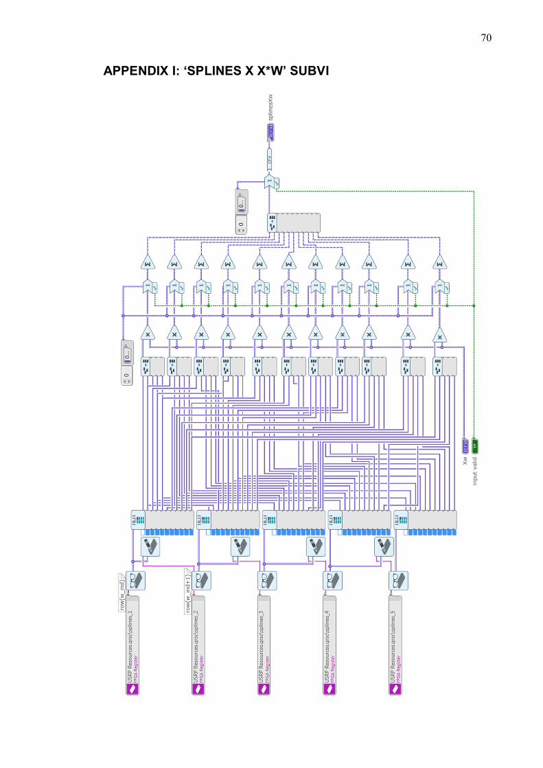
70
APPENDIX I: ‘SPLINES X X*W’ SUBVI

71
APPENDIX J: UI OF THE HOST PROGRAM

72
APPENDIX K: HOST CODE FOR DETERMINING DELAY AND DC-OFFSET