fpga-based pid controller implementation
TRANSCRIPT
FPGA-Based PID Controller Implementation�
Mohamed Abdelati
The Islamic University of Gaza
Gaza, Palestine
.
.
.
FPGAs
.
ها!$#ي!.
:مچلخ!
Abstract: Proportional-Integral-Derivative (PID) controllers are widely used in au-
tomation systems. They are usually implemented either in hardware using analog
components or in software using computer-based systems. They may also be imple-
mented using Application Specific Integrated Circuits (ASICs). This paper outlines
several modules necessary for building PID controllers on Field Programmable Gate
Arrays (FPGAs) which improve speed, accuracy, power, compactness, and cost ef-
fectiveness. Two PID controllers for speed and position utilizing these modules are
implemented and used as experimental platforms to illustrate and test the designed
modules.
1 Introduction
There are two approaches for implementing control systems using digital technol-
ogy. The first approach is based on software which implies a memory-processor
interaction. The memory holds the application program while the processor fetches,
decodes, and executes the program instructions. Programmable Logic Controllers
(PLCs), microcontrollers, microprocessors, Digital Signal Processors (DSPs), and
general purpose computers are tools for software implementation.
�This research was supported by the Ministry of Higher Education in Palestine.
1
On the other hand, the second approach is based on hardware. Early hardware
implementation is achieved by magnetic relays extensively used in old industry au-
tomation systems. It then became achievable by means of digital logic gates and
Medium Scale Integration (MSI) components. When the system size and complex-
ity increases, Application Specific Integrated Circuits (ASICs) are utilized. The
ASIC must be fabricated on a manufacturing line, a process that takes several
months, before it can be used or even tested [1]. FPGAs are configurable ICs and
used to implement logic functions. Early generations of FPGAs were most often
used as glue logic which is the logic needed to connect the major components of
a system. They were often used in prototypes because they could be programmed
and inserted into a board in a few minutes, but they did not always make it into the
final product. Today’s high-end FPGAs can hold several millions gates and have
some significant advantages over ASICs. They ensure ease of design, lower de-
velopment costs, more product revenue, and the opportunity to speed products to
market. At the same time they are superior to software-based controllers as they are
more compact, power-efficient, while adding high speed capabilities [2].
The target FPGA device used in this research is Spartan-3 manufactured recently
by Xilinx [3]. Design development and debugging is carried on a low-cost, full
featured kit provided by Digilent [4]. This board, which costs less than a 100$,
provides all the tools required to quickly begin designing and verifying Spartan-3
platform designs. While the implemented modules are also suited to other high den-
sity FPGAs, designs are based on 50 MHz clock and should be updated if different
frequency is used.
In control systems, the majority of actuating signals and sensor returns are analog
signals. Therefore, analog to digital and digital to analog conversion plays an im-
portant role in digital controllers. These converters are located at the boundary of
the digital controller. Usually there are some modules within the digital system
that facilitate communication with these converters. In addition, digital controllers
usually encompass input/output (I/O) modules to communicate with users. Push-
buttons and seven segment displays are well suited to small size and compact con-
trollers. Along with these four mentioned building blocks a pulse width modulation
(PWM) device and an optical encoder interface adapter will be designed. They are
used as building blocks in many control applications such as speed and position
control. One more building block for digital filters will be addressed in this work.
It is essential to implement transfer functions in PID controllers.
2
The rest of this paper is organized as follows. In Section 2 relevant work is ad-
dressed. In Section 3, the building blocks are constructed. In Section 4, experimen-
tal work is described. Finally in Section 5, conclusions and suggestions for future
work are outlined.
2 Relevant work
Modern FPGAs and their distinguishable capabilities have been advertised exten-
sively by FPGA vendors. Moreover, some refereed articles addressed the advan-
tages of utilizing these powerful chips [2][5]. In the past two years, Spartan II
and III FPGA families from Xilinx have been successfully utilized in a variety of
applications which include inverters [6][7], communications [8][9], imbedded pro-
cessors [10], and image processing [11].
The implementation of PID controllers using microprocessors and DSP chips is old
and well known [12][13], whereas very little work can be found in the literature on
how to implement PID controllers using FPGAs. The scheme proposed in [14] is
based on a distributed arithmetic algorithm where a Look-Up-table (LUT) mecha-
nism inside the FPGA is utilized. The contribution focused on power and area issues
while FPGA interfacing is totally unaddressed. In our work we introduce a simple
method for implementing PID controllers together with many related constructing
modules. Some other contributions focused on proposing algorithms for tuning the
coefficients of PID controllers using FPGAs while the controller itself is still im-
plemented in software. These contributions are considered complementary to our
work as they provide tools for building adaptive PID applications. In [15] [16] two
different algorithms for fuzzy PID gain conditioner algorithm are proposed. Both
are based on fuzzy control that tunes the PID controller on-line.
A PWM generator is introduced in [17]. However, only simulation results are
presented and the proposed algorithm results in greater consumption of FPGA re-
sources compared to our algorithm which is tested experimentally. However, de-
spite its complexity, the algorithm in [17] is superior in terms of harmonic content
and is more suited to inverter applications.
In [18] the authors describe the architecture of a data acquisition system for a
gamma-ray imaging camera. The system has been designed by using Xilinx Spar-
tan II devices and 12-bit parallel A/D converters. In our work, data acquisition for
3
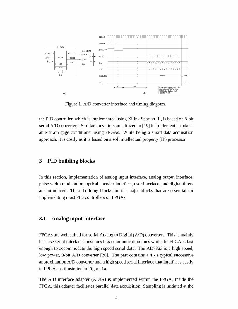
Sample
CONVST
SCLK
CLK50
int
The Data is latched from theinternal Input Sift Register(ISR) to the Output ShiftRegister (OSR)
1ms 4 sm
1 2 3 4 5 6 7 8Sin
1 2 3 4 5 6 7 8ISR
OSR=DB validunvalid
ADIA
int
(a) (b)
Figure 1. A/D converter interface and timing diagram.
the PID controller, which is implemented using Xilinx Spartan III, is based on 8-bit
serial A/D converters. Similar converters are utilized in [19] to implement an adapt-
able strain gage conditioner using FPGAs. While being a smart data acquisition
approach, it is costly as it is based on a soft intellectual property (IP) processor.
3 PID building blocks
In this section, implementation of analog input interface, analog output interface,
pulse width modulation, optical encoder interface, user interface, and digital filters
are introduced. These building blocks are the major blocks that are essential for
implementing most PID controllers on FPGAs.
3.1 Analog input interface
FPGAs are well suited for serial Analog to Digital (A/D) converters. This is mainly
because serial interface consumes less communication lines while the FPGA is fast
enough to accommodate the high speed serial data. The AD7823 is a high speed,
low power, 8-bit A/D converter [20]. The part contains a 4 � s typical successive
approximation A/D converter and a high speed serial interface that interfaces easily
to FPGAs as illustrated in Figure 1a.
The A/D interface adapter (ADIA) is implemented within the FPGA. Inside the
FPGA, this adapter facilitates parallel data acquisition. Sampling is initiated at the
4
SCLK
CLK50
The Data is latched fromthe control and databuses to the Output SiftRegister (OSR)
SYNC
Sout 12345678910111213141516
CB DB
OSRSout
VA
VB
AD 7303
Din
SYNCSYNC
DAIA
(a) (b)
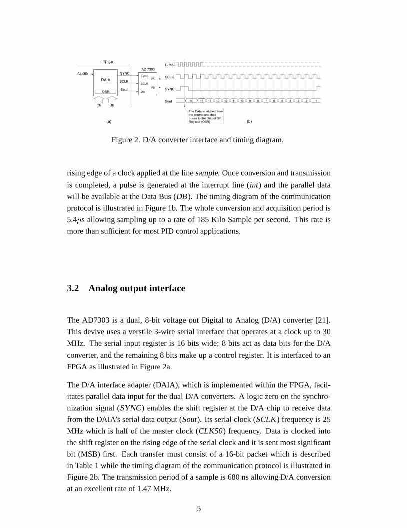
Figure 2. D/A converter interface and timing diagram.
rising edge of a clock applied at the line sample. Once conversion and transmission
is completed, a pulse is generated at the interrupt line (int ) and the parallel data
will be available at the Data Bus (DB ). The timing diagram of the communication
protocol is illustrated in Figure 1b. The whole conversion and acquisition period is
5.4 � s allowing sampling up to a rate of 185 Kilo Sample per second. This rate is
more than sufficient for most PID control applications.
3.2 Analog output interface
The AD7303 is a dual, 8-bit voltage out Digital to Analog (D/A) converter [21].
This devive uses a verstile 3-wire serial interface that operates at a clock up to 30
MHz. The serial input register is 16 bits wide; 8 bits act as data bits for the D/A
converter, and the remaining 8 bits make up a control register. It is interfaced to an
FPGA as illustrated in Figure 2a.
The D/A interface adapter (DAIA), which is implemented within the FPGA, facil-
itates parallel data input for the dual D/A converters. A logic zero on the synchro-
nization signal (SYNC ) enables the shift register at the D/A chip to receive data
from the DAIA’s serial data output (Sout ). Its serial clock (SCLK ) frequency is 25
MHz which is half of the master clock (CLK50 ) frequency. Data is clocked into
the shift register on the rising edge of the serial clock and it is sent most significant
bit (MSB) first. Each transfer must consist of a 16-bit packet which is described
in Table 1 while the timing diagram of the communication protocol is illustrated in
Figure 2b. The transmission period of a sample is 680 ns allowing D/A conversion
at an excellent rate of 1.47 MHz.
5
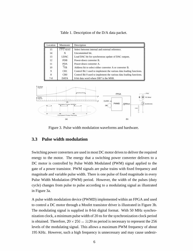
Table 1. Description of the D/A data packet.
Location Mnemonic Description
15 ����� /EXT Select between internal and external reference.
14 X Uncommitted bit.
13 LDAC Load DAC bit for synchronous update of DAC outputs.
12 PDB Power-down converter B.
11 PDA Power-down converter A.
10 � /B Address bit to select either converter A or converter B.
9 CR1 Control Bit 1 used to implement the various data loading functions.
8 CR0 Control Bit 0 used to implement the various data loading functions.
7-0 DATA 8-bit data word where DB7 is the MSB.
Constant Pulse Periods
Variable Pulse Widths
a
t
t
AnalogSignal
PWMSignal
Sampling Period
DBPWMoutPWMD
Vcc
DC Motor
BUK555-60A
220W
M
(a) (b)
Figure 3. Pulse width modulation waveforms and hardware.
3.3 Pulse width modulation
Switching power converters are used in most DC motor drives to deliver the required
energy to the motor. The energy that a switching power converter delivers to a
DC motor is controlled by Pulse Width Modulated (PWM) signal applied to the
gate of a power transistor. PWM signals are pulse trains with fixed frequency and
magnitude and variable pulse width. There is one pulse of fixed magnitude in every
Pulse Width Modulation (PWM) period. However, the width of the pulses (duty
cycle) changes from pulse to pulse according to a modulating signal as illustrated
in Figure 3a.
A pulse width modulation device (PWMD) implemented within an FPGA and used
to control a DC motor through a Mosfet transistor driver is illustrated in Figure 3b.
The modulating signal is supplied in 8-bit digital format. With 50 MHz synchro-
nization clock, a minimum pulse width of 20 ns for the synchronization clock period
is obtained. Therefore, � �������������� ns period is necessary to represent the 256
levels of the modulating signal. This allows a maximum PWM frequency of about
195 KHz. However, such a high frequency is unnecessary and may cause undesir-
6
DB
BOEIA
A
I
Optic
al Encoder
Channel A
Channel B
Index
Channel A
Channel B
Index
1 cycle
90o
clockwise
(a) (b)
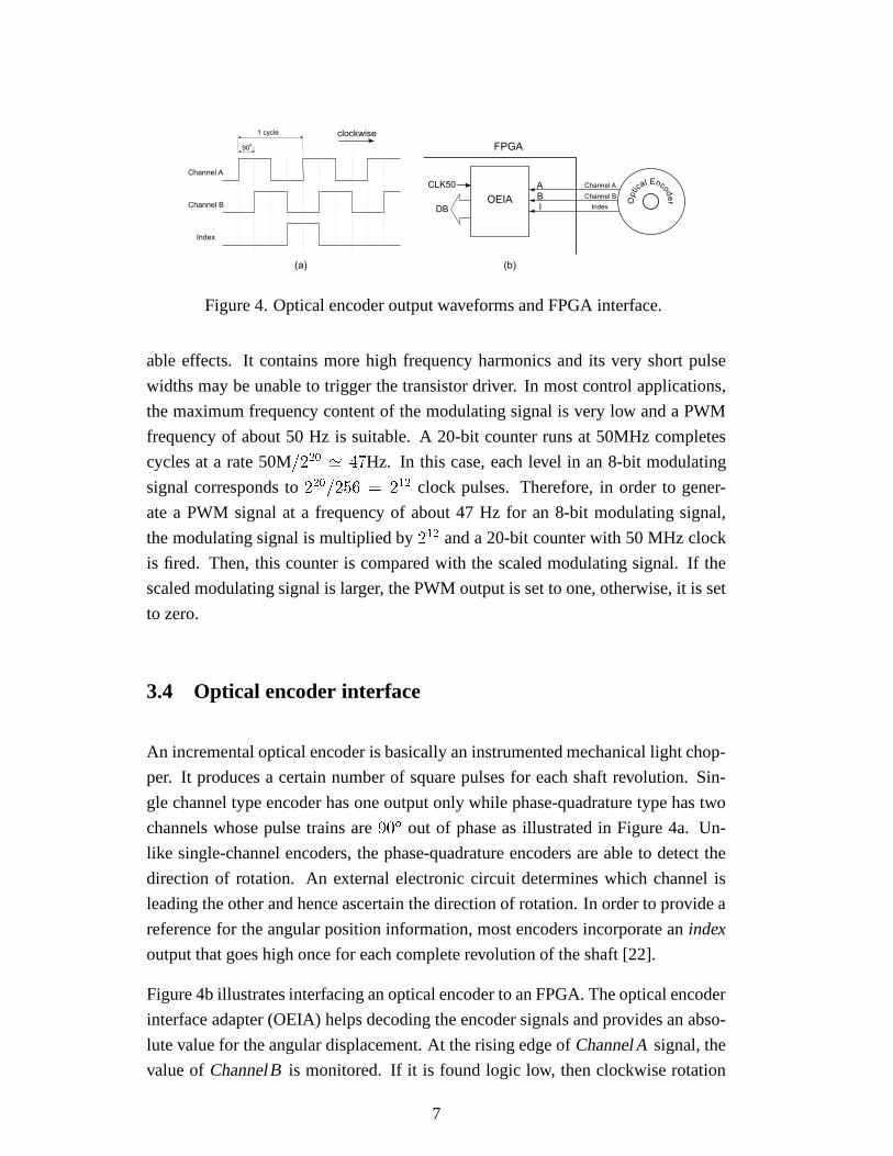
Figure 4. Optical encoder output waveforms and FPGA interface.
able effects. It contains more high frequency harmonics and its very short pulse
widths may be unable to trigger the transistor driver. In most control applications,
the maximum frequency content of the modulating signal is very low and a PWM
frequency of about 50 Hz is suitable. A 20-bit counter runs at 50MHz completes
cycles at a rate 50M ����������! Hz. In this case, each level in an 8-bit modulating
signal corresponds to ��� ������"�#%$ � clock pulses. Therefore, in order to gener-
ate a PWM signal at a frequency of about 47 Hz for an 8-bit modulating signal,
the modulating signal is multiplied by �$ � and a 20-bit counter with 50 MHz clock
is fired. Then, this counter is compared with the scaled modulating signal. If the
scaled modulating signal is larger, the PWM output is set to one, otherwise, it is set
to zero.
3.4 Optical encoder interface
An incremental optical encoder is basically an instrumented mechanical light chop-
per. It produces a certain number of square pulses for each shaft revolution. Sin-
gle channel type encoder has one output only while phase-quadrature type has two
channels whose pulse trains are &��' out of phase as illustrated in Figure 4a. Un-
like single-channel encoders, the phase-quadrature encoders are able to detect the
direction of rotation. An external electronic circuit determines which channel is
leading the other and hence ascertain the direction of rotation. In order to provide a
reference for the angular position information, most encoders incorporate an index
output that goes high once for each complete revolution of the shaft [22].
Figure 4b illustrates interfacing an optical encoder to an FPGA. The optical encoder
interface adapter (OEIA) helps decoding the encoder signals and provides an abso-
lute value for the angular displacement. At the rising edge of ChannelA signal, the
value of ChannelB is monitored. If it is found logic low, then clockwise rotation
7
DBPBIA
4.7KWBCD
CLK50
DOUN
UPVCC1
100W
SSIA
4.7KW VCC2
T2A42
3
0123456
01
2
3
4
5
6
7
2 1 0
Row
Column
7
Common anode
PB(1)
PB(0)
Figure 5. Push-buttons and multiplexed 7-segment displays interfacing.
is concluded and the value of DB is incremented by one. On the other hand, if
ChannelB is found logic high, counterclockwise rotation is inferred, and hence, the
value of DB is decremented by one. The Index signal is asynchronous as it is eval-
uated before ChannelA rising edge action. Once this signal is detected, the value
of DB is reset. This helps initial condition setup and also run-time correction for
any possible drift caused by noise.
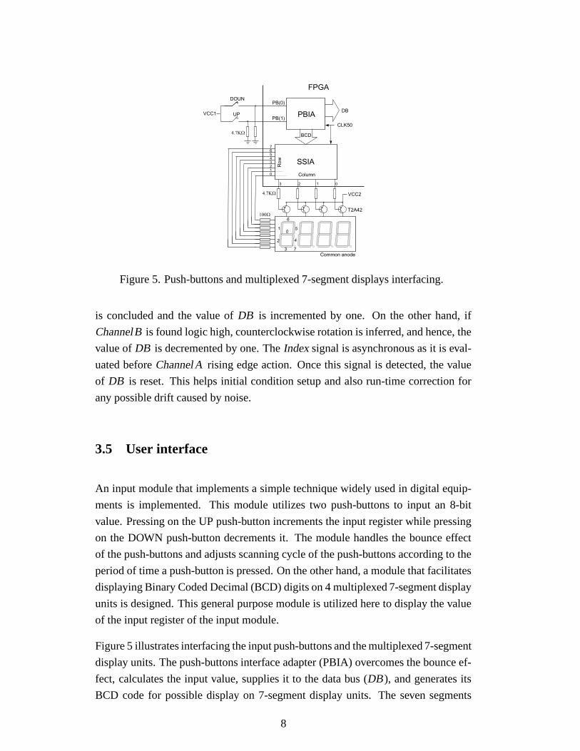
3.5 User interface
An input module that implements a simple technique widely used in digital equip-
ments is implemented. This module utilizes two push-buttons to input an 8-bit
value. Pressing on the UP push-button increments the input register while pressing
on the DOWN push-button decrements it. The module handles the bounce effect
of the push-buttons and adjusts scanning cycle of the push-buttons according to the
period of time a push-button is pressed. On the other hand, a module that facilitates
displaying Binary Coded Decimal (BCD) digits on 4 multiplexed 7-segment display
units is designed. This general purpose module is utilized here to display the value
of the input register of the input module.
Figure 5 illustrates interfacing the input push-buttons and the multiplexed 7-segment
display units. The push-buttons interface adapter (PBIA) overcomes the bounce ef-
fect, calculates the input value, supplies it to the data bus (DB ), and generates its
BCD code for possible display on 7-segment display units. The seven segments
8
interface adapter (SSIA) accepts a 16-bit BCD number and generates the scan pat-
terns necessary to display the coded decimal number on the 7-segment display units
which are multiplexed at a rate of 1KHz.
The bounce effect is eliminated by scanning the push-buttons at a rate with time
period larger than the bounce time of the push-buttons. A bounce might last for
few tens of milliseconds. Therefore, the default scanning period used in the PBIA,
which is about 167.77 ms, cancels the bounce effect and yet allows fast sensitivity
for the input. This scan period is made adaptive according to the last 5 input samples
of the push-buttons. This history information about the input samples is used to
adjust the scan rate.
3.6 Digital filters
While integer addition, subtraction, and multiplication operators are inferred by the
synthesis tool, division as well as floating point arithmetic are not supported. When
the divisor is an order of 2, division may be carried easily by shift operation. How-
ever, when the divisor is an arbitrary number, division is not straight forward and
considered to be a difficult and time consuming operation. Little is available in the
literature for VHDL source code of floating point arithmetic modules. Although
there are some limited contributions available on the Internet [23], they are not of-
ficially refereed and tested by experts. The majority of contributions are not open
source and sold commercially as Intellectual Property (IP) cores [24]. While they
are not free, IP cores consume a substantial amount of the FPGA resources. One
may avoid division in filter implementation by some normalization tricks. To illus-
trate these methods and compare their performance, consider the transfer function
of a first order filter given by
(*),+%- �. ),+%-/ ),+%- �
0�21
0$+!3 $
� 154 $+ 3 $ (1)
The time domain relationship between the input 6 and the output 7 at time 8 is given
by
7 ) 8 - � 0 � 6) 8 - 1
0$ 6) 8:9;� - 9 4 $ 7
) 8:9;� - (2)
In order to avoid floating point computation, the designer should restrict all data
9
representation to be integers. The communication with all interface devices is al-
ready specified to have 8-bit data width. Therefore, in order to calculate the right
hand side of Equation 2 using 2’s complement arithmetic, the coefficients must be
rounded to integers. Unfortunately, this will not work as most of these coefficients
are usually less than one or they spread a very small part of the available data do-
main. This can best be illustrated by examining the coefficients of the following
filter which is used in the position controller example that is given in next section.
7 ) 8 - �<&>= ��?�&�6 ) 8 - 9@&>=A�B�%?�6 ) 8�9;� - 1 >= C��%�B7) 8�9;� - (3)
One way to overcome this trouble is to scale the equation by a suitable large number
( D ) which is an order of 2 so that the scaled coefficients in the right side are fairly
spread and rounded. Then the number of bits required to represent these scaled
coefficients are determined. Denoting the integer rounding operator by EGF , then
Equation 3 is approximated by
7 ) 8 - �HE EID0� F�6) 8 - 1 EID
0$ F�6) 8:9;� - 1 E�9JD 4 $ F�7
) 8:9;� -D F (4)
Since D is chosen to be a power of 2, division is simply handled by shifting opera-
tion. This approach while being easy will not provide satisfactory results whatever
the value of D . This is because D helps only to increase the resolution of the filter
coefficients. But there is another source of error which is rounding the value of 7each time, the fact that it influences the upcoming values in this recursive formula.
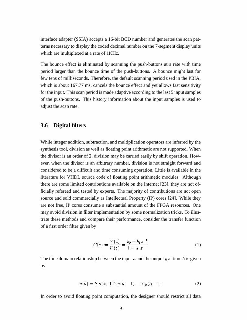
This crude approximation method is used in the filter example specified in Equa-
tion 3 with DK�L�M� . The resulting unit step response is shown in Figure 6 and
labeled “Crude approximation.”
In order to achieve fine approximation, the amount of information lost after each
recursive iteration should be reduced. This can be done by keeping the quantity
DN�O7 ) 8 - instead of 7 ) 8 - and utilizing it in the upcoming iteration. This approach
leads to
D � 7 ) 8 - �PEID � 0 � F�6) 8 - 1 EID �
0$ F�6) 8:9;� - 9QEID 4 $ FG�@E
DN�R7 ) 8S9T� -D F (5)
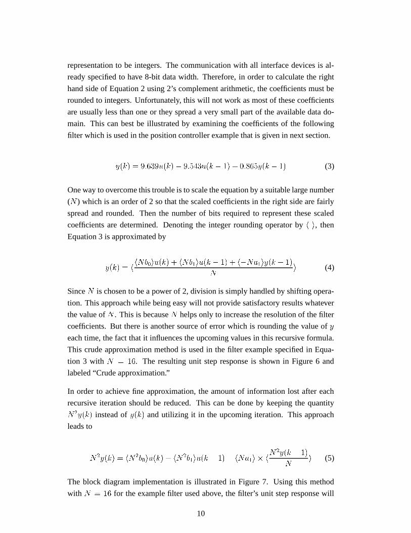
The block diagram implementation is illustrated in Figure 7. Using this method
with DU�V�M� for the example filter used above, the filter’s unit step response will
10
10
5 10 15 20 25 30
8
6
4
2
Filt
er
ou
tpu
t
k
Exact
Fine approximation
Crude approximation
Figure 6. Unit step response of the filter.
Input 8-bits
u(k) u(k-1) Ny(k-1)
-a N1 xxx
S
SS
Output 8-bits
b N1
2b N0
2
bit[15:8] bit[7] bit[3]bit[15:4]
8-bit 12-bit
21-bit
8-bit
13-bit 13-bit 5-bit
N = 16
a = - 0.865
b = 9.639
b = - 9.543
1
0
1
N y(k)2
Figure 7. Implementing Equation 5.
be as shown in Figure 6. It is labeled “Fine approximation” in the figure.
4 Experimental work
This section aims to integrate the modules designed earlier in some practical exam-
ples so that they are tested and illustrated. The first example is a standard DC-motor
speed control while the other one addresses demonstration of position control of an
unmanned electrical dual rotor helicopter.
4.1 DC-motor speed controller
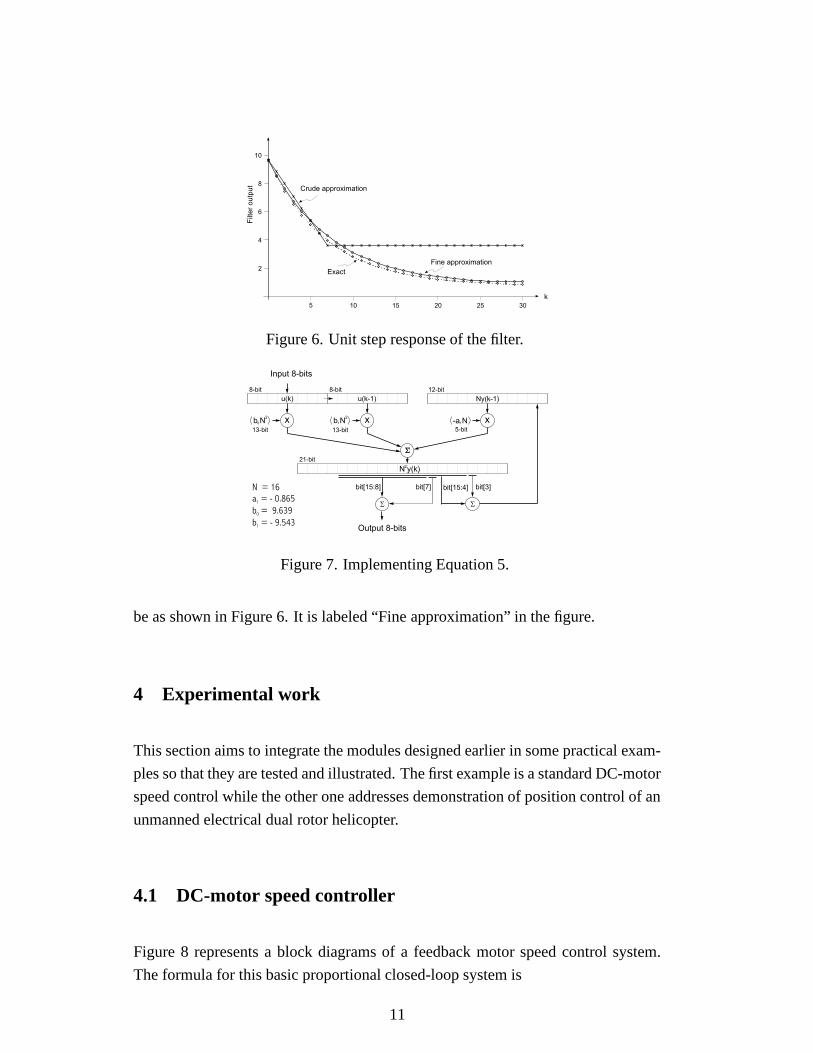
Figure 8 represents a block diagrams of a feedback motor speed control system.
The formula for this basic proportional closed-loop system is
11
DC to PWM(unity gain)A
1r S
w
y( s+1)t1 ( s+1)t2
A
A
BDC Motor
++
KS-+
Tachometer(unity gain)
S+
+
Figure 8. Proportional feedback control of a DC-Motor.
y
M G
mechanicalcoupling
12V
+ +
100nF
BUK555-60A220W
AD7823ADIA
PWMD
SSIA
PBIA S
-
+S
+K
Rx
R =10KWp
ry
+
Speed_Controller
Psi
PsiRef
YYbuf
CLK50
Figure 9. DC-motor speed control using FPGA.
W )IX�- �Y1 �)[Z
$X1 �
-\)[Z�X1 �
-1Y WJ] )IX�- 1
^)[Z$X1 �
-\)[Z�X1 �
-1YQ_ )IX�-
(6)
whereY
is the gain of the proportional controller,Z$ and
Z� , as well as the con-
stants^
and ` (appears in the figure) are expressed in terms of the DC motor
variables [25].Wa] )IX�-
and _ )IX�-are the Laplace transforms of the reference speed)cb ] )[de-e-
and the load torque ( f )[de- ) respectively. If these quantities are constants,
that isb ] )[de- � b ] and f )[de- �Qf , then the steady-state speed is given by
b2gIg � b ] 1^
) � 1Y - f (7)
The DC motor used in this experimental example has a rated voltage 12V, a rated
speed 2500 rpm, and equipped with a tachometer which generates 18V at rated
speed. A value of K=64 is found suitable for a good dynamic response of the
system. Using FPGA technology, the system may be implemented as illustrated
in Figure 9. The input module (PBIA) is supposed to handle entering the reference
speed which will be any value from 0 to 2500 or as a percentage from 0% to 100%.
12
However, as 8-bit A/D converter will be used to read the actual speed, it makes no
sense to have very fine reference speed specification. As the actual speed will be
quantized to a maximum of 256 levels, the reference speed is better specified in 256
or less levels. Taking the speed step to be 10, a total of 250 steps will be used to
cover the whole speed range.
The feedback signal is a low pass signal. Thus, the voltage divider and the capacitor
at the entrance of the A/D converter are implemented to act as a low pass filter that
suppresses any potential high frequency noise. Moreover, the voltage divider acts
as a signal conditioner device that maps the sensor signal to the convertible input
range of the A/D converter. In this experiment a 3.3V reference voltage is used for
the converter which implies that in order to utilize the whole range of the converter
the range of the feedback signal should be treated to be from 0 to 3.3V. As the rated
speed will be represented by the number 250, its corresponding input voltage will
be ?>= ?h� ��i����i�i �j?>=A�?%��?%k . Therefore, the voltage divider ratio is
lnmlpoq� ?>=A�?%��?
�MC �j>=r�� �&%
A �M�sut sensitive potentiometer is used to implement this voltage divider. It should
be noted that these precise calculations are just to clarify design steps and method-
ology. However, realization is easier; once the system is built, a certain reference
speed is set and the actual speed is measured using a tachometer. Then the poten-
tiometer is adjusted so that the measured speed is matched to the input reference
speed.
The top-level module of the motor controller will utilize the PBIA, SSIA, ADIA,
and PWMD modules developed earlier. Therefore, these components are declared
and instanced properly. The module basically consists of 3 processes: The first one
generates the sampling clock from CLK50. The maximum permissible sampling
clock frequency is 185 KHz which is determined by the A/D converter as mentioned
in Section 3.1. For this simple application, sampling clock frequency in the order
of few hundreds is sufficient. This clock is connected to the “Sample” port of
ADIA. Consequently, this adapter generates interrupt pulses at its port “int” after
each sample acquisition as illustrated earlier in Figure 1. These pulses are used to
synchronize the other two processes. One process works at the rising edge of the
“int” signal to calculate the unsaturated output while the other process works at
the falling edge of the “int” signal to register this output after handling saturation
conditions.
13
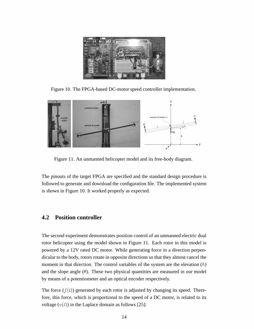
Figure 10. The FPGA-based DC-motor speed controller implementation.
potentiometer
optical encoder
counterwight
x
y
z
h
mg
moment of inertia =J
l
l
Figure 11. An unmanned helicopter model and its free-body diagram.
The pinouts of the target FPGA are specified and the standard design procedure is
followed to generate and download the configuration file. The implemented system
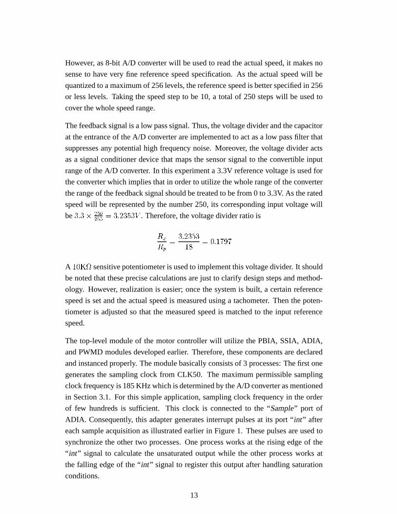
is shown in Figure 10. It worked properly as expected.
4.2 Position controller
The second experiment demonstrates position control of an unmanned electric dual
rotor helicopter using the model shown in Figure 11. Each rotor in this model is
powered by a 12V rated DC motor. While generating force in a direction perpen-
dicular to the body, rotors rotate in opposite directions so that they almost cancel the
moment in that direction. The control variables of the system are the elevation ( v )
and the slope angle ( w ). These two physical quantities are measured in our model
by means of a potentiometer and an optical encoder respectively.
The force ( x )[de- ) generated by each rotor is adjusted by changing its speed. There-
fore, this force, which is proportional to the speed of a DC motor, is related to its
voltage ( y )[de- ) in the Laplace domain as follows [25]:
14

z$)IX�- � { $ ` $ k $
)IX�-)[Z$�$X1 �
-\)[Z$ �X1 �
- (8)
z�)IX�- � { � ` � k �
)IX�-)[Z� $X1 �
-\)[Z���X1 �
- (9)
where { $ , ` $ ,Z$�$ ,Z$ � , { � , ` � ,
Z� $ , and
Z��� are constants. The angular acceleration
along the x-axis equals the net torque in this direction divided by the model’s mo-
ment of inertia ( | ) at the axis of rotation. Therefore, the angular displacement ( w )is given by
}h)IX�- � ) z $)IX�- 9 z �
)IX�-e-�~| X � (10)
where ~ is the force-arm length. The net vertical force is the summation of the two
forces multiplied by cos( w ) minus the effective weight of the model1. However,
since w is small, the cosine factor may be safely dropped. The resultant vertical
acceleration equals the net vertical force divided by the model’s effective mass ( � ).
Therefore, the vertical displacement ( v ) is given by
� )IX�- � ) z $)IX�-1z�)IX�- 9"��� - �
� X � (11)
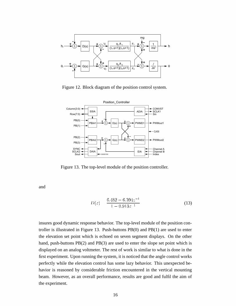
where � is the acceleration of gravity. This described feedback control system may
be modeled as shown in Figure 12. In this system, v ] and w ] represent the reference
points of the elevation and slope respectively while v and w are the actual measured
values. The error signal in v influences both forces in the same direction whereas
the error signal in w influences them in opposite directions. The elevation and slope
controllers are decoupled to simplify design and implementation.
This model is digitized and Matlab is used for simulation and estimation of the PID
filters’ parameters. It is found that
(*),+%- � &>= ��?�&a9@&>=A�B�%? +!3 $��9@>= C��%� + 3 $ (12)
1Similar to elevators, a counter weight is used to minimize the force necessary to move the body.
Therefore, the effective mass ( � ) equals the mass of the main body minus the mass used in the
counter weight. Equivalently, the effective weight equals the weight of the main body minus the
counter weight.
15
S
-
+ +G(s)
-+
S
S+
D(s)
+
S
+S
+
+S
( s+1)t11 ( s+1)t12
( s+1)t21 ( s+1)t22
1
ms2
Js2
h
q
h
q
r
r
q A1 1
q A2 2 l
mg
F1
F2
V1
V2
Figure 12. Block diagram of the position control system.
PWMD2
PWMD1
SSIA
PBIA1
S
-
+ +G(s)
Position_Controller
PBIA2
-+
S
S+
D(s)
+S
DAIA
PB(0)
PB(1)
PB(2)
PB(3)
SYNC
Sout
Column(3:0)
Row(7:0)ADIA
EIAChannel AChannel BIndex
CONVSTSCLK1Sin
SCLK2
PWMout1
PWMout2
00000100
CLK50
Figure 13. The top-level module of the position controller.
and
� ),+%- � �>= �%C%J9@�>= ?�&�� +!3 $��9">= &>�M? + 3 $ (13)
insures good dynamic response behavior. The top-level module of the position con-
troller is illustrated in Figure 13. Push-buttons PB(0) and PB(1) are used to enter
the elevation set point which is echoed on seven segment displays. On the other
hand, push-buttons PB(2) and PB(3) are used to enter the slope set point which is
displayed on an analog voltmeter. The rest of work is similar to what is done in the
first experiment. Upon running the system, it is noticed that the angle control works
perfectly while the elevation control has some lazy behavior. This unexpected be-
havior is reasoned by considerable friction encountered in the vertical mounting
beam. However, as an overall performance, results are good and fulfil the aim of
the experiment.
16
5 Conclusions
Today’s high-speed and high-density FPGAs provide viable design alternatives to
ASIC and microprocessor-based implementations. Several building modules for
implementing PID controllers on these FPGAs are constructed in this work. These
modules are tested successfully through two experimental platforms.
Algorithms and implementations are described in sufficient details from a practical
point of view for readers to digest the addressed subject and replicate the work. The
VHDL code of all presented modules and examples may be obtained directly from
the author.
Implementing PID controllers on FPGAs features speed, accuracy, power, com-
pactness, and cost improvement over other digital implementation techniques. In a
future fork we plan to investigate implementation of fuzzy logic controllers on FP-
GAs. Also we plan to explore embedded soft processors, such as MicroBlaze, and
study some applications in which design partitioning between software and hard-
ware provides better implementations.
Acknowledgment: The author is grateful to his Fulbright host at Texas A&M uni-
versity, Dr. Reza Langari, for his kind company and helpful research environment.
References
[1] G. Martin and H. Chang, “System-on-Chip design”, Proceedings of the 4th interna-
tional conference on ASIC, Oct. 2001, pp. 12-17.
[2] Anthony Cataldo, “Low-priced FPGA options set to expand” Electronic Engineering
Times Journal, N 1361, PP 38-45, USA 2005.
[3] Xilinx, “Spartan-3 FPGA Family: Complete Data Sheet” 2004.
http://www.xilinx.com/bvdocs/publications/ds099.pdf
[4] Digilent, Inc., “Digilent Spartan-3 System Board”, June, 2004.
http://www.digilentinc.com/Data/Products/S3BOARD/S3BOARD-brochure.pdf
[5] Gordon Hands, “Optimised FPGAs vs dedicated DSPs”, Electronic Product Design
Journal, V 25, N 12, UK December 2004.
17
[6] R. Jastrzebski, A. Napieralski,O. Pyrhonen, H. Saren, “Implementation and simula-
tion of fast inverter control algorithms with the use of FPGA circuit”, 2003 Nanotech-
nology Conference and Trade Show, pp 238-241, Nanotech 2003.
[7] Lin, F.S.; Chen, J.F.; Liang, T.J.; Lin, R.L.; Kuo, Y.C. “Design and implementation
of FPGA-based single stage photovoltaic energy conversion system”, Proceedings of
IEEE Asia-Pacific Conference on Circuits and Systems, pp 745-748, Taiwan, Dec.
2004.
[8] Bouzid Aliane and Aladin Sabanovic, “Design and implementation of digital band-
pass FIR filter in FPGA”, Computers in Education Journal, v14, p 76-81, 2004.
[9] M. Canet, F. Vicedo,V. Almenar, J. Valls, “FPGA implementation of an IF transceiver
for OFDM-based WLAN”, IEEE Workshop on Signal Processing Systems, SiPS: De-
sign and Implementation, PP 227-232, USA 2004.
[10] Xizhi Li, Tiecai Li, “ECOMIPS: An economic MIPS CPU design on FPGA”, Pro-
ceedings - 4th IEEE International Workshop on System-on-Chip for Real-Time Ap-
plications, PP 291-294, Canada 2004.
[11] R. Gao, D. Xu,J. P. Bentley, “Reconfigurable hardware implementation of an im-
proved parallel architecture for MPEG-4 motion estimation in mobile applications”,
IEEE Transactions on Consumer Electronics, V49, N4, November 2003.
[12] H. D. Maheshappa, R. D. Samuel, A. Prakashan, “Digital PID controller for speed
control of DC motors”, IETE Technical Review Journal, V6, N3, PP171-176, India
1989.
[13] J. Tang, “PID controller using the TMS320C31 DSK with on-line parameter adjust-
ment for real-time DC motor speed and position control”, IEEE International Sympo-
sium on Industrial Electronics, V2, PP 786-791, Pusan 2001.
[14] Y. F. Chan, M. Moallem, W. Wang, “Efficient implementation of PID control algo-
rithm using FPGA technology”, Proceedings of the 43ed IEEE Conference on Deci-
sion and Control, V5, PP. 4885-4890, Bahamas 2004.
[15] Bao-Sheng Hu, Jing Li, “Fuzzy PID gain conditioner: Algorithm, architecture and
FPGA implementation”, Journal of Engineering and Applied Science, PP 621-624,
US 1996.
[16] Wei Jiang, Jianbo Luo, “Realization of fuzzy controller with parameters PID self-
tuning by combination of software and hardware”, Proceedings of the Second Inter-
national Symposium on Instrumentation Science and Technology, V1, PP 407-410,
China 2002.
18
[17] D. Deng, S. Chen,G. Joos, “FPGA implementation of PWM pattern generators”,
Canadian Conference on Electrical and Computer Engineering, V1, PP 225-230 May
2001. and Electronics Engineers Inc.
[18] K. Nurdan, T. Conka-Nurdana, H. J. Beschc, B. Freislebenb, N. A. Pavelc, A. H. Wa-
lentac, “FPGA-based data acquisition system for a Compton camera”, Proceedings of
the 2nd International Symposium on Applications of Particle Detectors in Medicine,
Biology and Astrophysics, V510, N1, PP. 122-125, Sep 2003.
[19] S. Poussier, H. Rabah, S. Weber, “Smart Adaptable Strain Gage Conditioner: Hard-
ware/Software Implementation”, IEEE Sensors Journal, V4, N2, April 2004.
[20] Analog Devices Inc., “2.7 V to 5.5 V, 5 � s, 8-Bit ADC in 8-Lead microSOIC/DIP”,
2000.
http://www.analog.com/UploadedFiles/Data Sheets/216007123AD7823 c.pdf
[21] Analog Devices Inc., “+2.7 V to +5.5 V, Serial Input, Dual Voltage Output 8-Bit
DAC”, 1997.
http://www.analog.com/UploadedFiles/Data Sheets/48853020AD7303 0.pdf
[22] S. Holle, “Incremental Encoder Basics”, Sensors, April 1990, pp.22-30.
[23] J. Detrey, “A VHDL Library of Parametrisable Floating-Point and LNS Operators for
FPGA”, 2003.
http://perso.ens-lyon.fr/jeremie.detrey/FPLibrary/FPLibrary-0.9.tgz
[24] Transtech DSP, “Quixilica Floating Point FPGA Cores”, 2002.
http://www.transtech-dsp.com/datasheets/qx-dsp001-fp hm v1.pdf
[25] G. Franklin, J. Powell, and A. Emami-Naeini, “Feedback control of dynamic sys-
tems”, Addison-Wesley, 4th ed., 2002.
[26] R. Coughlin and F. Driscoll, “Operational Amplifiers and Linear Integrated Circuits”,
Prentice Hall, 6th ed., 2000.
19