fpga implementation of digital systems == practical ... · fpga implementation of digital systems...
TRANSCRIPT
1
FPGA Implementation of Digital Systems == Practical Activities ==
Lecturer PhD Eng Ionel BOSTAN University of Pitesti Romania
17-21/ Oct / 2016/ Perugia
2
1. Hardware support ; 2. Software support; 3. Applications
FPGA Implementation of Digital Systems – Practical Activities
What is FPGA ? – Actual trend in the implementation of digital systems is to use
reconfigurable circuits like FPGA
“You can configure these chips to implement custom hardware
functionality without ever having to pick up a breadboard or soldering iron”
– Advantage of FPGA (Field-Programmable Gate Array)
– Large number of digital circuits which can be interconnected by the end
user by software means (using a configuration bitstream);
Bitstream contains information on how the components should be wired together .
– Completely reconfigurable - instantly take on a brand new “personality” when you recompile a different configuration of circuitry (a new bitstream);
– Easy to use – mature high-level design tools are available;
– Low cost do to the mass production;
17-21/ Oct / 2016/ Perugia
3
1. Hardware support ; 2. Software support; 3. Applications
FPGA Implementation of Digital Systems – Practical Activities
Why we insist on teaching FPGA ?
Student Perspective:
- students have the feeling that they working in software;
- easy to develop and test new application (even without learn a
hardware description language like Verilog or VHDL);
- increased chances of finding a god job;
Technical advantage:
- Easy to use: “You can configure these chips to implement custom hardware functionality without ever having to pick up a breadboard or soldering iron” ;
- Large number of digital circuits which can be interconnected by the end user by software means
- Completely reconfigurable: in case of mistake in design, just fix your "logic function", re-compile and re-download it.
- Low cost do to the mass production;
17-21/ Oct / 2016/ Perugia
4
1. Hardware support ; 2. Software support; 3. Applications
FPGA Implementation of Digital Systems – Practical Activities
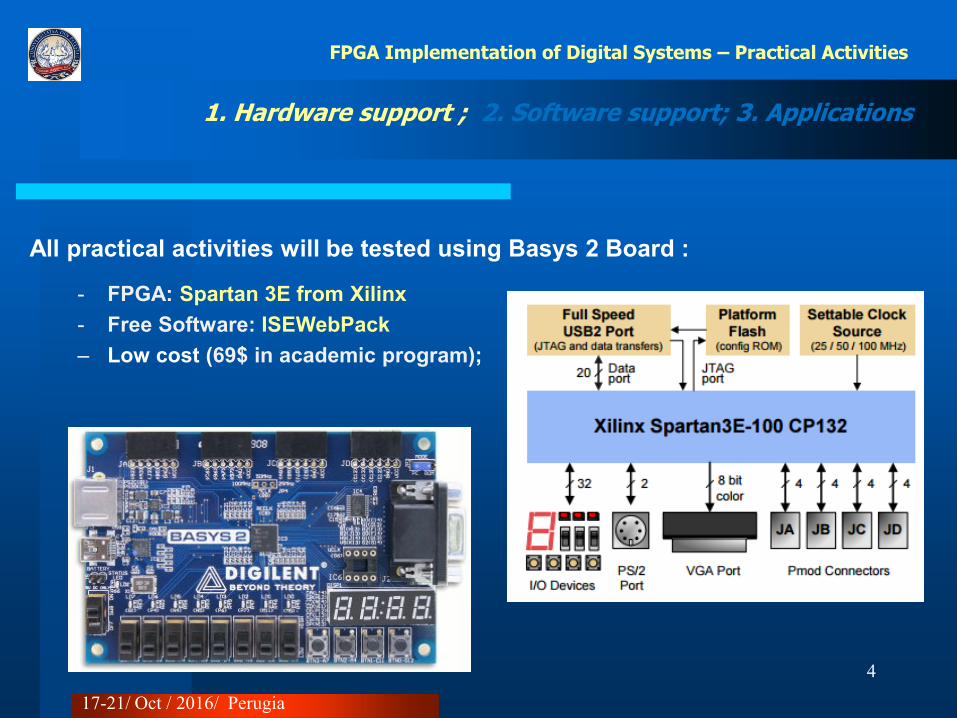
All practical activities will be tested using Basys 2 Board :
- FPGA: Spartan 3E from Xilinx
- Free Software: ISEWebPack
– Low cost (69$ in academic program);
17-21/ Oct / 2016/ Perugia
5
1. Hardware support ; 2. Software support; 3. Applications
FPGA Implementation of Digital Systems – Practical Activities
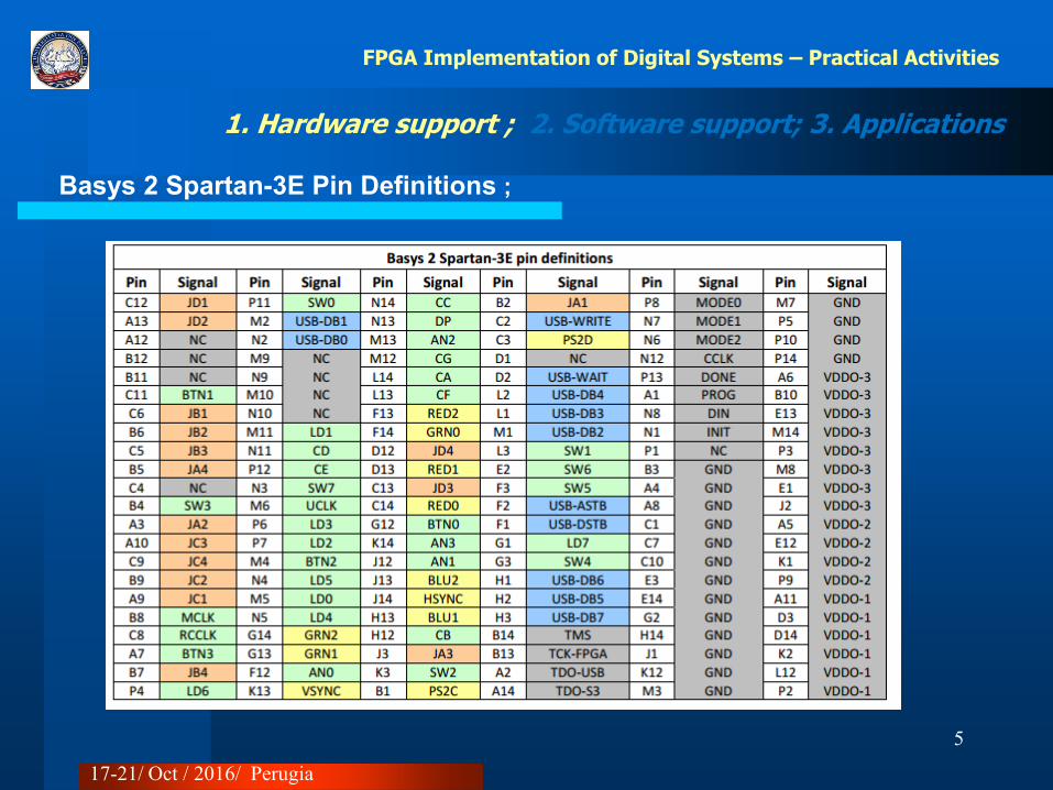
Basys 2 Spartan-3E Pin Definitions ;
17-21/ Oct / 2016/ Perugia
6
1. Hardware support ; 2. Software support; 3. Applications
FPGA Implementation of Digital Systems – Practical Activities
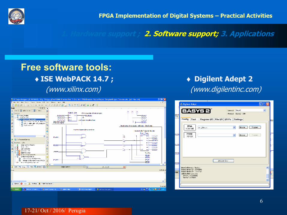
Free software tools: ISE WebPACK 14.7 ; Digilent Adept 2
(www.xilinx.com) (www.digilentinc.com)
17-21/ Oct / 2016/ Perugia
7
1. Hardware support ; 2. Software support; 3. Applications
FPGA Implementation of Digital Systems – Practical Activities
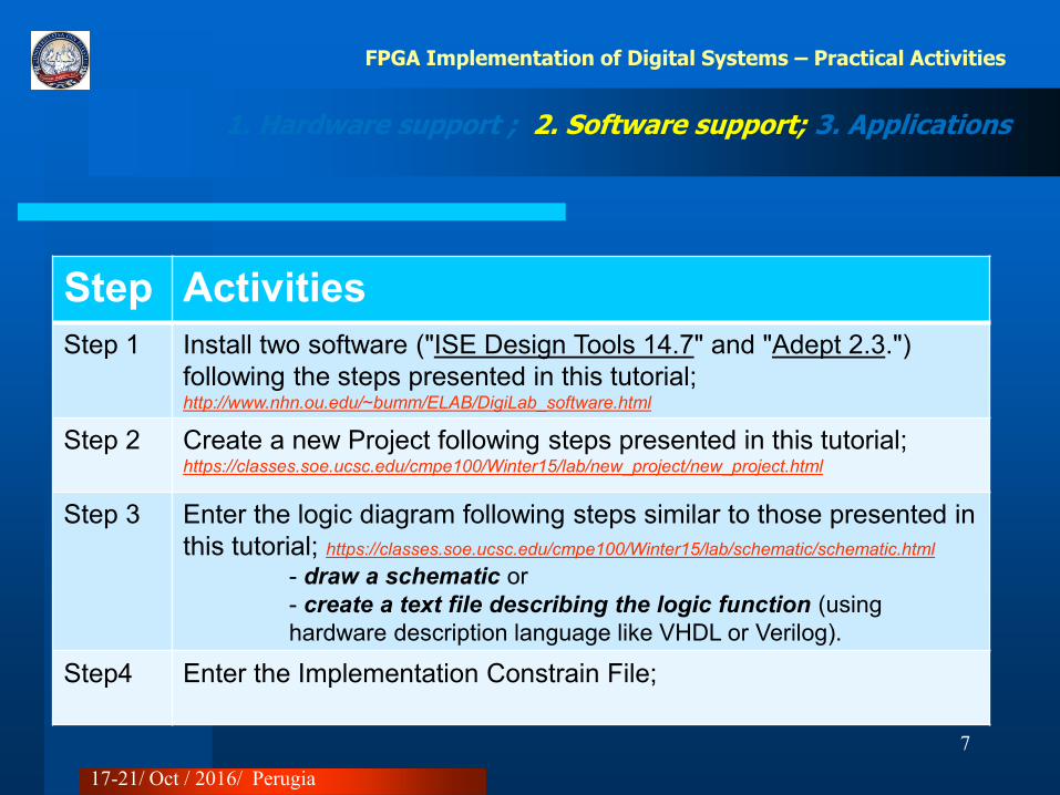
Step Activities
Step 1 Install two software ("ISE Design Tools 14.7" and "Adept 2.3.")
following the steps presented in this tutorial; http://www.nhn.ou.edu/~bumm/ELAB/DigiLab_software.html
Step 2
Create a new Project following steps presented in this tutorial; https://classes.soe.ucsc.edu/cmpe100/Winter15/lab/new_project/new_project.html
Step 3
Enter the logic diagram following steps similar to those presented in
this tutorial; https://classes.soe.ucsc.edu/cmpe100/Winter15/lab/schematic/schematic.html
- draw a schematic or
- create a text file describing the logic function (using
hardware description language like VHDL or Verilog).
Step4 Enter the Implementation Constrain File;
17-21/ Oct / 2016/ Perugia
8
1. Hardware support ; 2. Software support; 3. Applications
FPGA Implementation of Digital Systems – Practical Activities
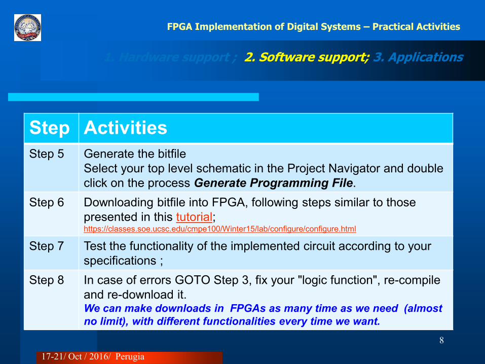
Step Activities
Step 5 Generate the bitfile
Select your top level schematic in the Project Navigator and double
click on the process Generate Programming File.
Step 6 Downloading bitfile into FPGA, following steps similar to those
presented in this tutorial; https://classes.soe.ucsc.edu/cmpe100/Winter15/lab/configure/configure.html
Step 7 Test the functionality of the implemented circuit according to your
specifications ;
Step 8
In case of errors GOTO Step 3, fix your "logic function", re-compile
and re-download it. We can make downloads in FPGAs as many time as we need (almost
no limit), with different functionalities every time we want.
17-21/ Oct / 2016/ Perugia
9
1. Hardware support ; 2. Software support; 3. Applications
FPGA Implementation of Digital Systems – Practical Activities
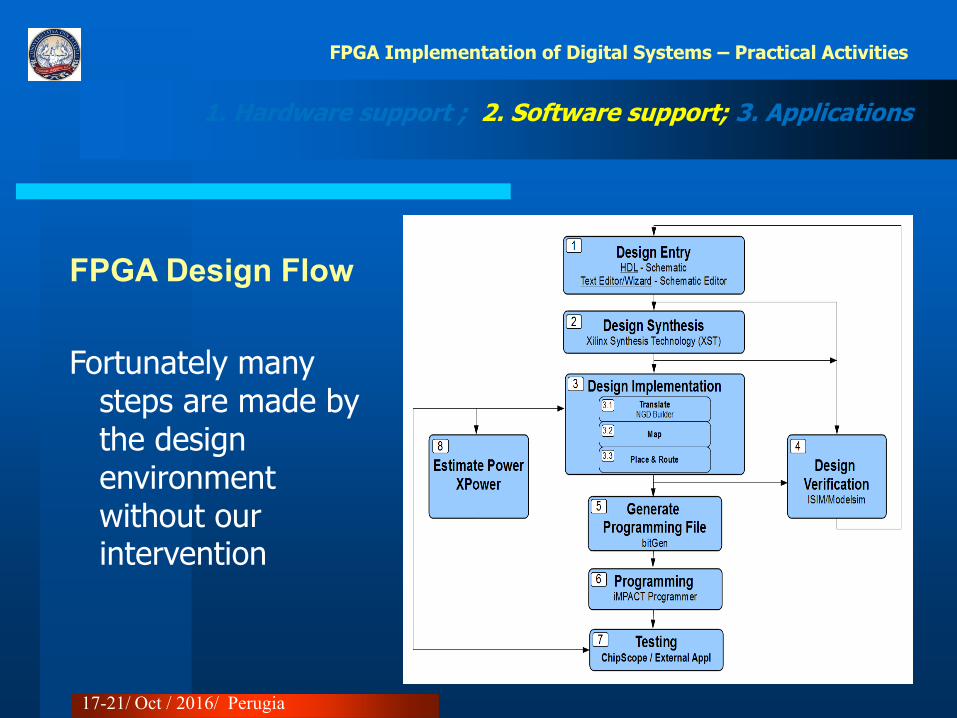
FPGA Design Flow
Fortunately many steps are made by the design environment without our intervention
17-21/ Oct / 2016/ Perugia
10
1. Hardware support ; 2. Software support; 3. Applications
FPGA Implementation of Digital Systems – Practical Activities
Practical aspects: - Working with FPGA is not an easy task for beginners;
- In each project, for any provider, it is mandatory to have a minimal specification and source file:
- specify the target FPGA – in our case we work with Spartan 3E-100 CP132;
- at least one source file to describe the circuit (schematic or text);
- at least one constrain file to specify how external devices are connected to the FPGA pins;
- To make things easier, in each practical application, you will use one Template Project in which there are already implemented some circuits that are necessary for testing different circuits;

17-21/ Oct / 2016/ Perugia
11
1. Hardware support ; 2. Software support; 3. Applications
FPGA Implementation of Digital Systems – Practical Activities
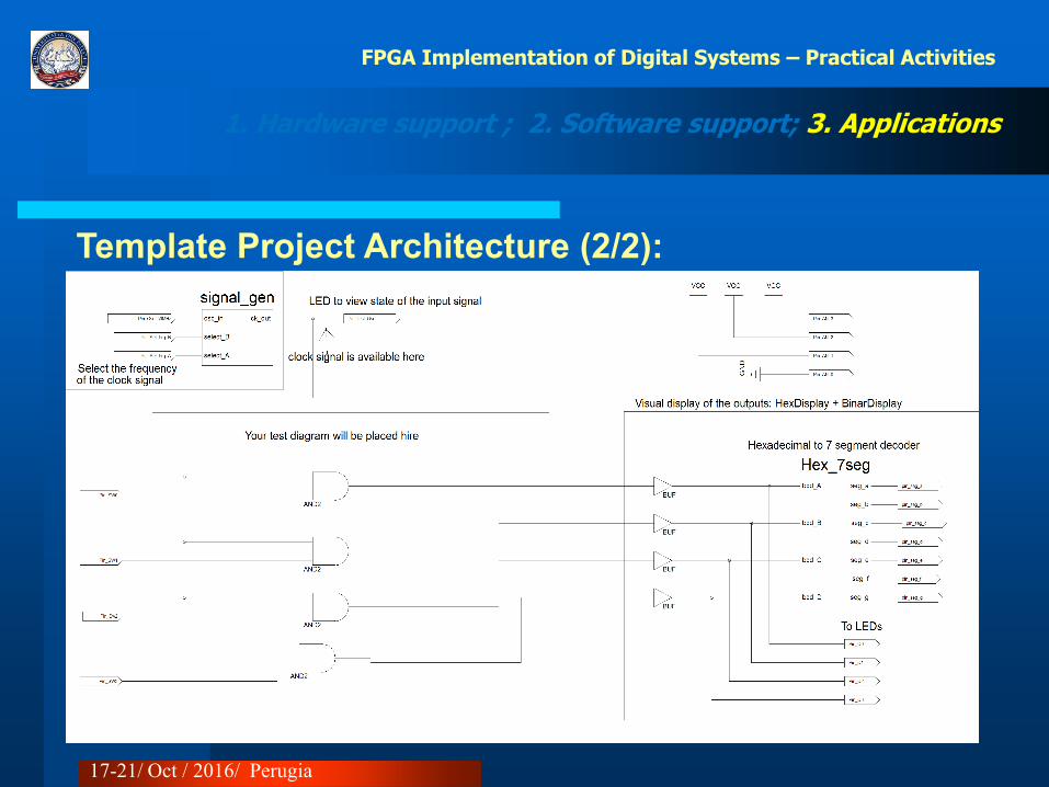
Project template architecture (1/2):
In Project_Template there are already implemented some circuits that are necessary for testing different circuits with counters or frequency dividers:
- Signal generator – to provide the clock signal for counting under test. This generator has two inputs which are used to change the frequency of the clock signal. These control inputs are connected board switches SW7 and SW6.
- HexDisplay – to display the state of the counter, in numeric format, on one of the four digits of the Basys2 board.
- BinDisplay – to display the state of the counter, in binary format, using the last four LEDs of the Basys2 board, LD3 to LD0.
- One Working Area - where you will put your project;
17-21/ Oct / 2016/ Perugia
12
1. Hardware support ; 2. Software support; 3. Applications
FPGA Implementation of Digital Systems – Practical Activities
Template Project Architecture (2/2):
17-21/ Oct / 2016/ Perugia
13
1. Hardware support ; 2. Software support; 3. Applications
FPGA Implementation of Digital Systems – Practical Activities
Example 1: Implement and test Project Template
Steps to follow:
Step 1: Start Project_Template
• Copy Project_Template folder on your computer;
• Find Project_Template.xise and double-click on this file;
• In Hierarchy Window double-click on Sch_bloc.sch;
Step 2: Generate configuration file:
• click one time on Design Tab;
• click one time on Sch_bloc.sch in Hierarchy Window;
• double-click on Generate Programming File in Processes Window;
• wait until obtain green light on Generate Programming File.
17-21/ Oct / 2016/ Perugia
14
1. Hardware support ; 2. Software support; 3. Applications
FPGA Implementation of Digital Systems – Practical Activities
Example 1: Implement and test Project Template
Steps to follow:
Step 3: Configure the FPGA board (download configuration file):
• Connect USB cable between PC and Basys2 board and then turn on the power (put switch SW8 in ON position);
• Start Digilent Adept and browse in project folder and find sch_bloc.bit;
• Then click on Program Button and ignore (click Yes) some warning;
Step 4: Test the circuit functionality:
• Put SW7 and SW6 in lower position to select the lower frequency of clock signal;
• Try different combination on last 4 switches (SW3 to SW0) and see what happens on the display and what happens with the last 4 LEDs (LD3 to LD0);
• Change position on SW6 and see what happens with frequency of clock signal. Try different combination on SW7 and SW6 to see the possibilities of the signal generator.
17-21/ Oct / 2016/ Perugia
15
1. Hardware support ; 2. Software support; 3. Applications
FPGA Implementation of Digital Systems – Practical Activities
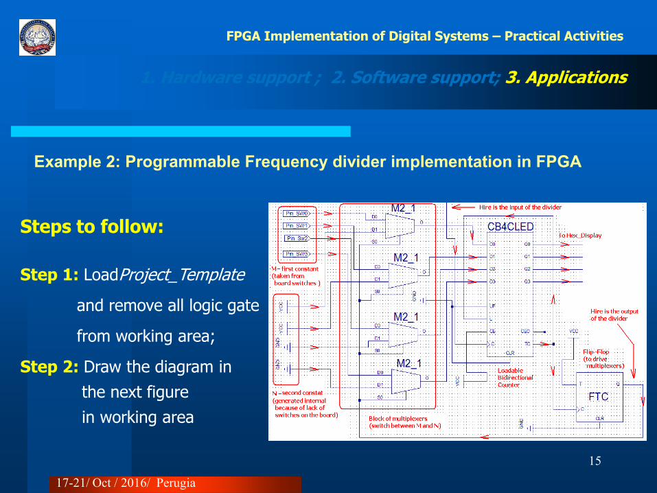
Example 2: Programmable Frequency divider implementation in FPGA
Steps to follow:
Step 1: LoadProject_Template
and remove all logic gate
from working area;
Step 2: Draw the diagram in
the next figure
in working area
17-21/ Oct / 2016/ Perugia
16
1. Hardware support ; 2. Software support; 3. Applications
FPGA Implementation of Digital Systems – Practical Activities
Example 2: Programmable Frequency divider implementation in FPGA
Steps to follow:
Step 3: Generating program file and then configure the FPGA;
Step 4: Test the circuit functionality:
• From switches SW7 and SW6 select the lowest frequency for the signal clock; • From switches SW3 and SW0 select M = 7 = 0111 and carefully analyze the operating mode of the divider;
17-21/ Oct / 2016/ Perugia
17
1. Hardware support ; 2. Software support; 3. Applications
FPGA Implementation of Digital Systems – Practical Activities
Example 3: Modify the previous project
Steps to follow:
Step 1: Load the previous project
Step 2: Add a supplementary output in schematic diagram
in order to see the logic state of the output signal.
For example you can use LD5 which is connected at pin N4.
Step 3: Add a supplementary line in constrain file
Step 4: Save the modification
Step 5: Remake the programming file and download in FPGA
Step 6: Verify the functionality of the implemented project
see how time signal stay in High state (LED lighting) and how time stay in Low state;
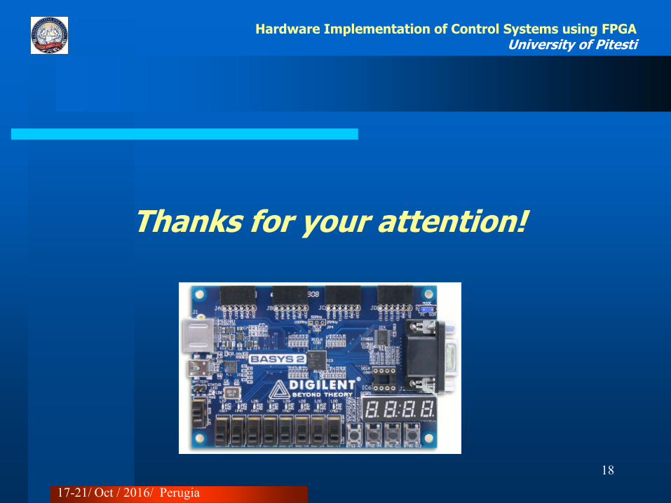
18
Hardware Implementation of Control Systems using FPGA University of Pitesti
Thanks for your attention!
17-21/ Oct / 2016/ Perugia