rd53 temperature sensors...global calibration with the ntc the global calibration consists in...
TRANSCRIPT
RD53 Temperature Sensors
July 9th, 2019 RD53 Temperature Sensors 1
M. MENOUNI
CPPM/Aix-Marseille Univ
On behalf of RD53 Collaboration
July 9th, 2019 RD53 Temperature Sensors 2
Outline
Sensors implemented in the RD53 chip
Principle of the Temperature sensor
Calibration
Temperature measurement through the ADC
Irradiation tolerance
Rpoly sensor
Overview of monitored currents and voltages
Conclusion
July 9th, 2019 RD53 Temperature Sensors 3
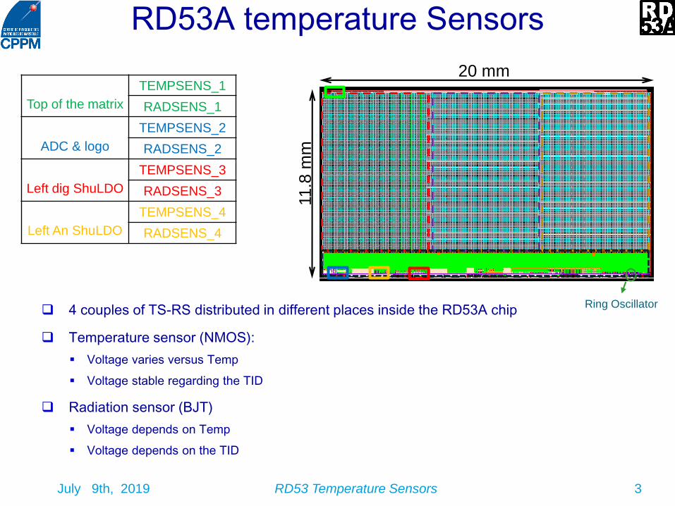
RD53A temperature Sensors
4 couples of TS-RS distributed in different places inside the RD53A chip
Temperature sensor (NMOS):
Voltage varies versus Temp
Voltage stable regarding the TID
Radiation sensor (BJT)
Voltage depends on Temp
Voltage depends on the TID
Top of the matrix
TEMPSENS_1
RADSENS_1
ADC & logo
TEMPSENS_2
RADSENS_2
Left dig ShuLDO
TEMPSENS_3
RADSENS_3
Left An ShuLDO
TEMPSENS_4
RADSENS_4
20 mm
11.8
mm
Ring Oscillator
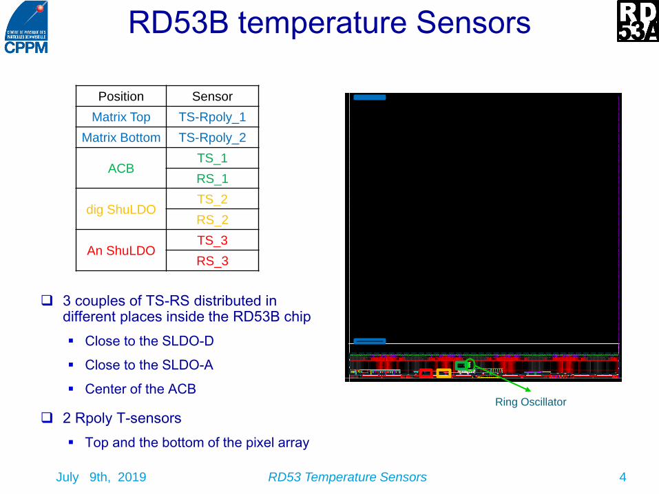
RD53B temperature Sensors
3 couples of TS-RS distributed in different places inside the RD53B chip
Close to the SLDO-D
Close to the SLDO-A
Center of the ACB
2 Rpoly T-sensors
Top and the bottom of the pixel array
July 9th, 2019 RD53 Temperature Sensors 4
Position Sensor
Matrix Top TS-Rpoly_1
Matrix Bottom TS-Rpoly_2
ACBTS_1
RS_1
dig ShuLDOTS_2
RS_2
An ShuLDOTS_3
RS_3
Ring Oscillator
Ring Oscillators
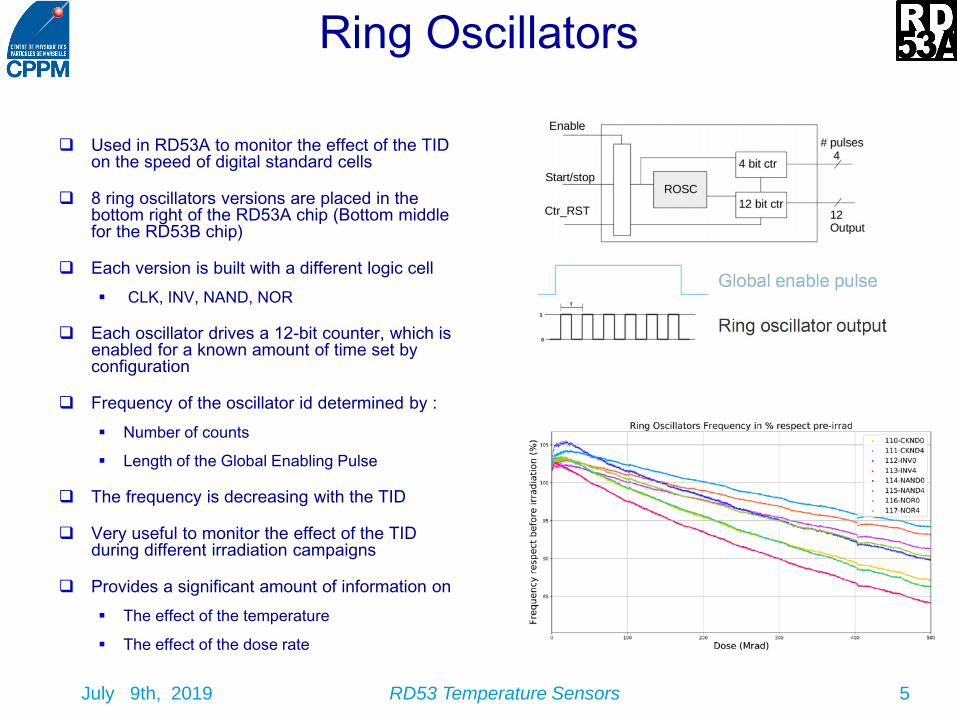
Used in RD53A to monitor the effect of the TID on the speed of digital standard cells
8 ring oscillators versions are placed in the bottom right of the RD53A chip (Bottom middle for the RD53B chip)
Each version is built with a different logic cell
CLK, INV, NAND, NOR
Each oscillator drives a 12-bit counter, which is enabled for a known amount of time set by configuration
Frequency of the oscillator id determined by :
Number of counts
Length of the Global Enabling Pulse
The frequency is decreasing with the TID
Very useful to monitor the effect of the TID during different irradiation campaigns
Provides a significant amount of information on
The effect of the temperature
The effect of the dose rate
July 9th, 2019 RD53 Temperature Sensors 5
July 9th, 2019 RD53 Temperature Sensors 6
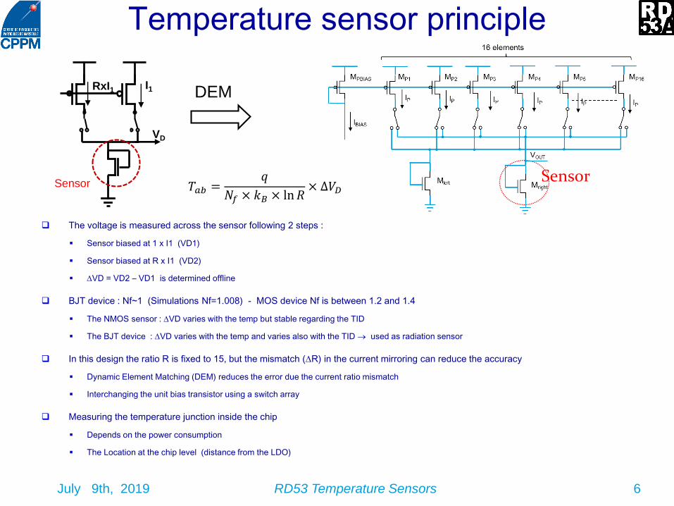
Temperature sensor principle
The voltage is measured across the sensor following 2 steps :
Sensor biased at 1 x I1 (VD1)
Sensor biased at R x I1 (VD2)
VD = VD2 – VD1 is determined offline
BJT device : Nf~1 (Simulations Nf=1.008) - MOS device Nf is between 1.2 and 1.4
The NMOS sensor : VD varies with the temp but stable regarding the TID
The BJT device : VD varies with the temp and varies also with the TID used as radiation sensor
In this design the ratio R is fixed to 15, but the mismatch (R) in the current mirroring can reduce the accuracy
Dynamic Element Matching (DEM) reduces the error due the current ratio mismatch
Interchanging the unit bias transistor using a switch array
Measuring the temperature junction inside the chip
Depends on the power consumption
The Location at the chip level (distance from the LDO)
VD
I1RxI1
Sensor 𝑇𝑎𝑏 =𝑞
𝑁𝑓 × 𝑘𝐵 × ln𝑅× ∆𝑉𝐷
Sensor
DEM
Global calibration with the NTC
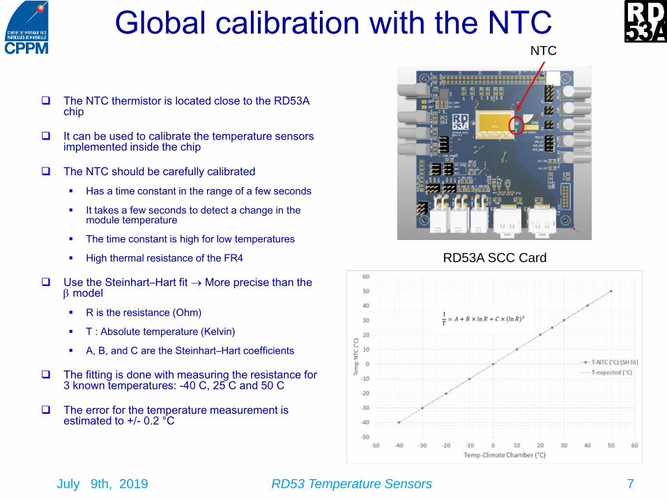
The NTC thermistor is located close to the RD53A chip
It can be used to calibrate the temperature sensors implemented inside the chip
The NTC should be carefully calibrated
Has a time constant in the range of a few seconds
It takes a few seconds to detect a change in the module temperature
The time constant is high for low temperatures
High thermal resistance of the FR4
Use the Steinhart–Hart fit More precise than the model
R is the resistance (Ohm)
T : Absolute temperature (Kelvin)
A, B, and C are the Steinhart–Hart coefficients
The fitting is done with measuring the resistance for 3 known temperatures: -40 C, 25 C and 50 C
The error for the temperature measurement is estimated to +/- 0.2 °C
July 9th, 2019 RD53 Temperature Sensors 7
RD53A SCC Card
NTC
Global calibration with the NTC
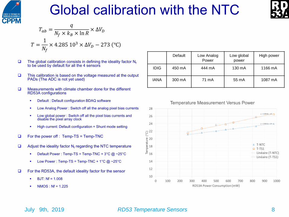
The global calibration consists in defining the ideality factor Nfto be used by default for all the 4 sensors
This calibration is based on the voltage measured at the output PADs (The ADC is not yet used)
Measurements with climate chamber done for the different RD53A configurations
Default : Default configuration BDAQ software
Low Analog Power : Switch off all the analog pixel bias currents
Low global power : Switch off all the pixel bias currents and disable the pixel array clock
High current: Default configuration + Shunt mode setting
For the power off : Temp-TS = Temp-TNC
Adjust the ideality factor Nf regarding the NTC temperature
Default Power : Temp-TS = Temp-TNC + 3°C @ ~25°C
Low Power : Temp-TS = Temp-TNC + 1°C @ ~25°C
For the RD53A, the default ideality factor for the sensor
BJT: Nf = 1.008
NMOS : Nf = 1.225
July 9th, 2019 RD53 Temperature Sensors 8
Default Low Analog
Power
Low global
power
High power
IDIG 450 mA 444 mA 130 mA 1166 mA
IANA 300 mA 71 mA 55 mA 1087 mA
𝑇 =1
𝑁𝑓× 4.285 103 × ∆𝑉𝐷 − 273 ℃
𝑇𝑎𝑏 =𝑞
𝑁𝑓 × 𝑘𝐵 × ln𝑅× ∆𝑉𝐷

July 9th, 2019 RD53 Temperature Sensors 9
Mismatch in the same chip
Measurements done for Direct Powering
Default power : 974 mW (Ivdda= 392 mA Ivddd=362 mA)
Default ideality factor :
BJT: Nf = 1.008
NMOS : Nf = 1.225
Small effect of the mismatch inside the same chip
For T>30°C Temp(TS) is higher than expected (+3°C at 50°C)
The power Increase with the temperature can explain a part of this error
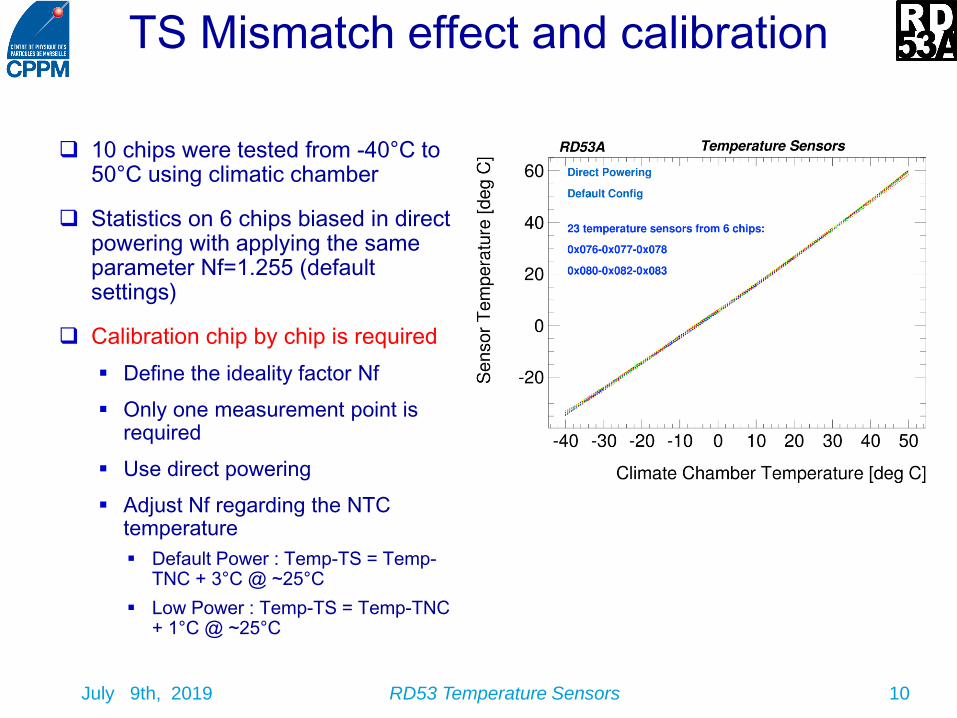
TS Mismatch effect and calibration
10 chips were tested from -40°C to 50°C using climatic chamber
Statistics on 6 chips biased in direct powering with applying the same parameter Nf=1.255 (default settings)
Calibration chip by chip is required
Define the ideality factor Nf
Only one measurement point is required
Use direct powering
Adjust Nf regarding the NTC temperature
Default Power : Temp-TS = Temp-TNC + 3°C @ ~25°C
Low Power : Temp-TS = Temp-TNC + 1°C @ ~25°C
July 9th, 2019 RD53 Temperature Sensors 10

Temperature measurement with ADC
The voltage reference can vary from chip to chip
The LSB should be measured chip by chip
Error introduced by the VREF variation versus the temperature
July 9th, 2019 RD53 Temperature Sensors 11
Irradiation effect
In the RD53A, the reference voltage is provided by a bandgap circuit
VREF shift of ~20 mV at 550 Mrad (~2%) LSB shift is around 2%
Error of ~2% of the absolute Temperature
An error of 6°C can be expected on the temperature measurement after 500 Mrad
OUT12 bit ADCVIN
SoC CLK
VREF
VREF
VD
DOUT
𝑉𝐷 = 𝐷𝑂𝑈𝑇 ×𝑉𝑅𝐸𝐹𝐴
= 𝐷𝑂𝑈𝑇 × 𝐿𝑆𝐵
VD
I1RxI1
𝑇𝑎𝑏 =𝑞
𝑁𝑓 × 𝑘𝐵 × ln𝑅× ∆𝑉𝐷
Method 1
𝑇𝑎𝑏 =𝑞
𝑁𝑓 × 𝑘𝐵 × ln𝑅× 𝐿𝑆𝐵 × 𝐷𝑂𝑈𝑇
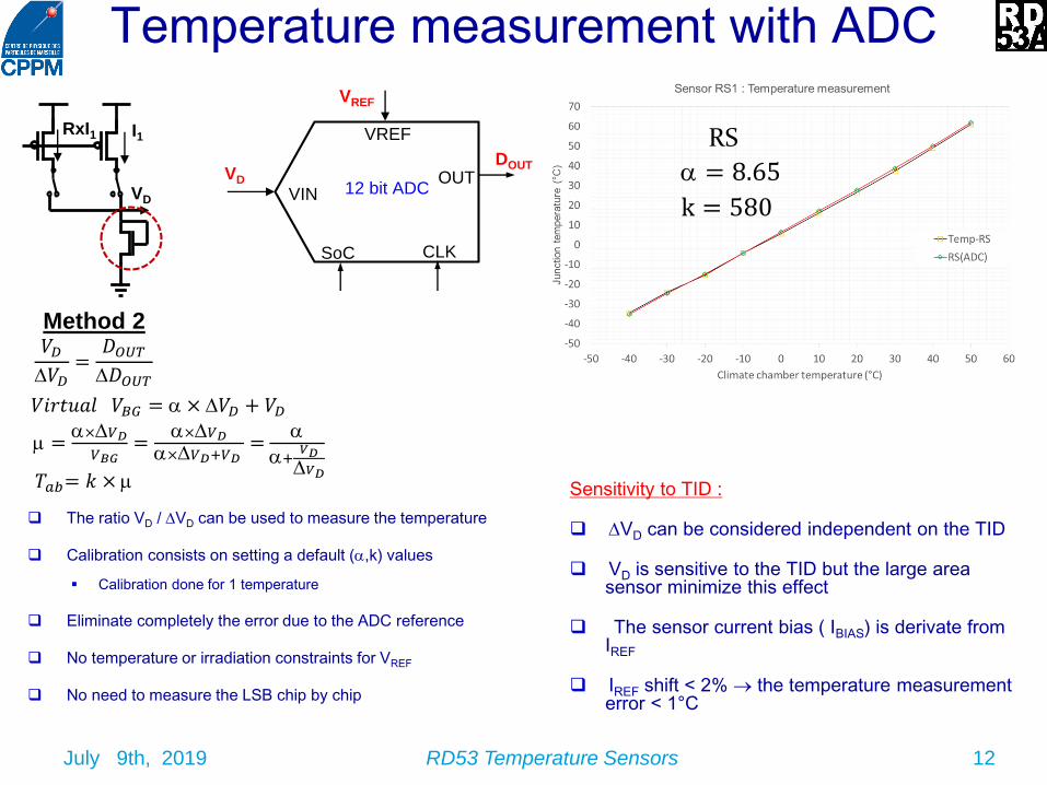
Temperature measurement with ADC
The ratio VD / VD can be used to measure the temperature
Calibration consists on setting a default (,k) values
Calibration done for 1 temperature
Eliminate completely the error due to the ADC reference
No temperature or irradiation constraints for VREF
No need to measure the LSB chip by chip
July 9th, 2019 RD53 Temperature Sensors 12
Sensitivity to TID :
VD can be considered independent on the TID
VD is sensitive to the TID but the large area sensor minimize this effect
The sensor current bias ( IBIAS) is derivate from IREF
IREF shift < 2% the temperature measurement error < 1°C
OUT12 bit ADCVIN
SoC CLK
VREF
VREF
VD
DOUT
=×𝑉𝐷
𝑉𝐵𝐺=
×𝑉𝐷×𝑉𝐷+𝑉𝐷
=
+𝑉𝐷
𝑉𝐷
𝑉𝐷𝑉𝐷
=𝐷𝑂𝑈𝑇𝐷𝑂𝑈𝑇
𝑉𝑖𝑟𝑡𝑢𝑎𝑙 𝑉𝐵𝐺 = × 𝑉𝐷 + 𝑉𝐷
VD
I1RxI1
𝑇𝑎𝑏= 𝑘 ×
Method 2
= 8.65
k = 580
RS
July 9th, 2019 RD53 Temperature Sensors 13
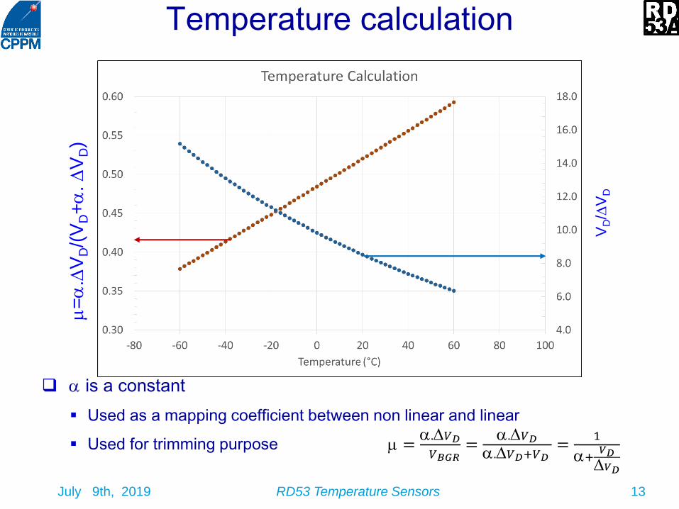
Temperature calculation
is a constant
Used as a mapping coefficient between non linear and linear
Used for trimming purpose
VD/
VD
=
.V
D/(
VD+
.
VD)
=.𝑉𝐷𝑉𝐵𝐺𝑅
=.𝑉𝐷
.𝑉𝐷+𝑉𝐷=
1
+𝑉𝐷
𝑉𝐷
July 9th, 2019 RD53 Temperature Sensors 14
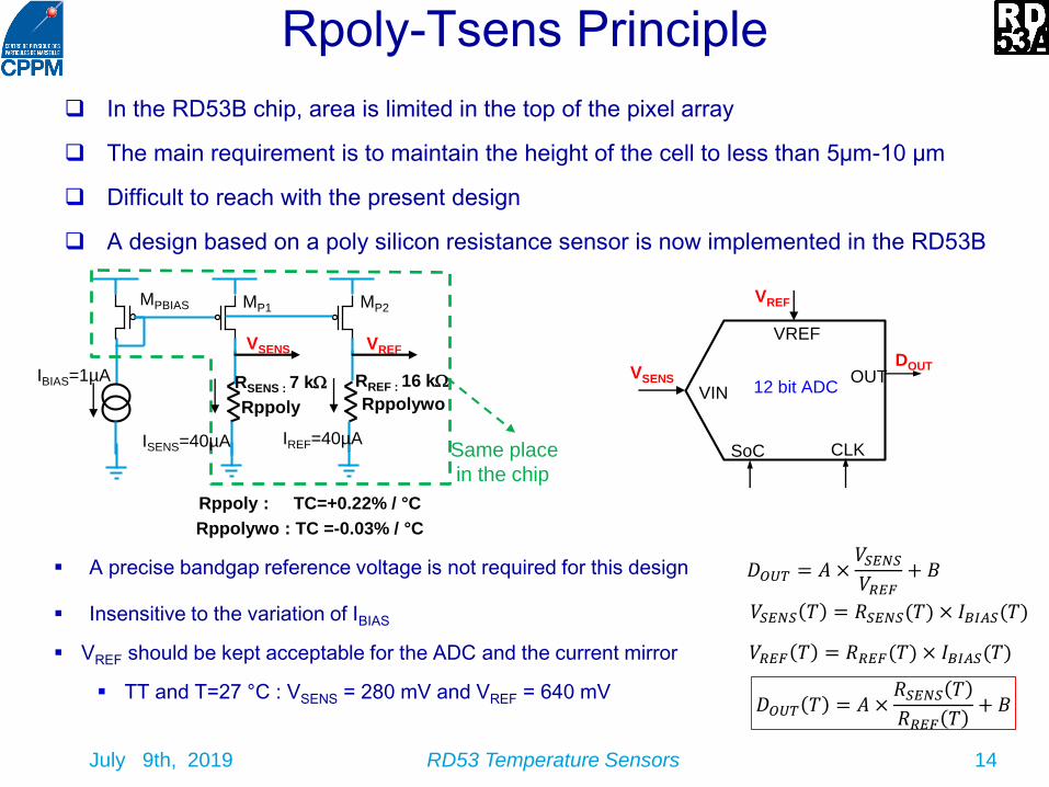
Rpoly-Tsens Principle
In the RD53B chip, area is limited in the top of the pixel array
The main requirement is to maintain the height of the cell to less than 5µm-10 µm
Difficult to reach with the present design
A design based on a poly silicon resistance sensor is now implemented in the RD53B
OUT12 bit ADCVIN
SoC CLK
VREF
VREF
VSENS
DOUT
𝑉𝑆𝐸𝑁𝑆 𝑇 = 𝑅𝑆𝐸𝑁𝑆(𝑇) × 𝐼𝐵𝐼𝐴𝑆(𝑇)
𝑉𝑅𝐸𝐹 𝑇 = 𝑅𝑅𝐸𝐹(𝑇) × 𝐼𝐵𝐼𝐴𝑆(𝑇)
𝐷𝑂𝑈𝑇 𝑇 = 𝐴 ×𝑅𝑆𝐸𝑁𝑆 𝑇
𝑅𝑅𝐸𝐹 𝑇+ 𝐵
𝐷𝑂𝑈𝑇 = 𝐴 ×𝑉𝑆𝐸𝑁𝑆𝑉𝑅𝐸𝐹
+ 𝐵 A precise bandgap reference voltage is not required for this design
Insensitive to the variation of IBIAS
VREF should be kept acceptable for the ADC and the current mirror
TT and T=27 °C : VSENS = 280 mV and VREF = 640 mV
Same place
in the chip
IBIAS=1µA
MPBIAS MP1
VREF
RREF : 16 k
MP2
VSENS
RSENS : 7 k
ISENS=40µA IREF=40µA
Rppoly Rppolywo
Rppoly : TC=+0.22% / °C
Rppolywo : TC =-0.03% / °C
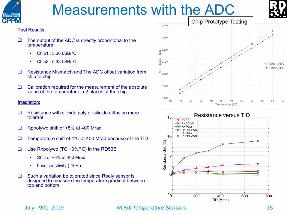
Measurements with the ADCTest Results
The output of the ADC is directly proportional to the temperature
Chip1 : 5.36 LSB/°C
Chip2 : 5.33 LSB/°C
Resistance Mismatch and The ADC offset variation from chip to chip
Calibration required for the measurement of the absolute value of the temperature in 2 places of the chip
Irradiation:
Resistance with silicide poly or silicide diffusion more tolerant
Rppolywo shift of +8% at 400 Mrad
Temperature shift of 4°C at 400 Mrad because of the TID
Use Rnpolywo (TC ~0%/°C) in the RD53B
Shift of +3% at 400 Mrad
Less sensitivity (-10%)
Such a variation be tolerated since Rpoly sensor is designed to measure the temperature gradient between top and bottom
July 9th, 2019 RD53 Temperature Sensors 15
Chip Prototype Testing
Resistance versus TID
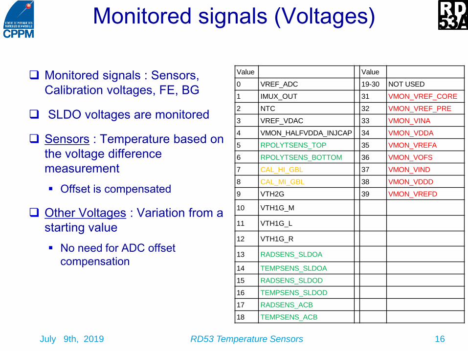
Monitored signals (Voltages)
Monitored signals : Sensors,
Calibration voltages, FE, BG
SLDO voltages are monitored
Sensors : Temperature based on
the voltage difference
measurement
Offset is compensated
Other Voltages : Variation from a
starting value
No need for ADC offset
compensation
July 9th, 2019 RD53 Temperature Sensors 16
Value Value
0 VREF_ADC 19-30 NOT USED
1 IMUX_OUT 31 VMON_VREF_CORE
2 NTC 32 VMON_VREF_PRE
3 VREF_VDAC 33 VMON_VINA
4 VMON_HALFVDDA_INJCAP 34 VMON_VDDA
5 RPOLYTSENS_TOP 35 VMON_VREFA
6 RPOLYTSENS_BOTTOM 36 VMON_VOFS
7 CAL_HI_GBL 37 VMON_VIND
8 CAL_MI_GBL 38 VMON_VDDD
9 VTH2G 39 VMON_VREFD
10 VTH1G_M
11 VTH1G_L
12 VTH1G_R
13 RADSENS_SLDOA
14 TEMPSENS_SLDOA
15 RADSENS_SLDOD
16 TEMPSENS_SLDOD
17 RADSENS_ACB
18 TEMPSENS_ACB
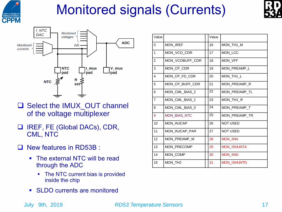
Monitored signals (Currents)
Select the IMUX_OUT channel of the voltage multiplexer
IREF, FE (Global DACs), CDR, CML, NTC
New features in RD53B :
The external NTC will be read through the ADC
The NTC current bias is provided inside the chip
SLDO currents are monitored
July 9th, 2019 RD53 Temperature Sensors 17
Value Value
0 MON_IREF 16 MON_TH1_M
1 MON_VCO_CDR 17 MON_LCC
2 MON_VCOBUFF_CDR 18 MON_VFF
3 MON_CP_CDR 19 MON_PREAMP_L
4 MON_CP_FD_CDR 20 MON_TH1_L
5 MON_CP_BUFF_CDR 21 MON_PREAMP_R
6 MON_CML_BIAS_2 22 MON_PREAMP_TL
7 MON_CML_BIAS_1 23 MON_TH1_R
8 MON_CML_BIAS_0 24 MON_PREAMP_T
9 MON_BIAS_NTC 25 MON_PREAMP_TR
10 MON_INJCAP 26 NOT USED
11 MON_INJCAP_PAR 27 NOT USED
12 MON_PREAMP_M 28 MON_IINA
13 MON_PRECOMP 29 MON_ISHUNTA
14 MON_COMP 30 MON_IIND
15 MON_TH2 31 MON_ISHUNTD
July 9th, 2019 RD53 Temperature Sensors 18
Conclusion
A temperature sensor calibration methodology is presented
Set default temperature coefficients
Adjust parameters chip by chip at a known temperature (mismatch)
The 12 bit ADC allows a good precision for the temperature measurement (<+/- 1°C) accurate measurement of VD
2 different methods for the temperature measurement with the ADC :
Method 1 : direct measurement and requires very stable and very radiation tolerant reference voltage
Method 2 : less constraining about the reference voltage
Irradiation tests at ambient temperature and high dose rate are in progress on the RD53A chip
A new temperature sensor based on Rpoly resistance is implemented in the RD53B
Measure the temperature variation between the top and the bottom of the chip
July 9th, 2019 RD53 Temperature Sensors 19
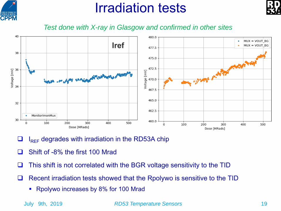
Irradiation tests
IREF degrades with irradiation in the RD53A chip
Shift of -8% the first 100 Mrad
This shift is not correlated with the BGR voltage sensitivity to the TID
Recent irradiation tests showed that the Rpolywo is sensitive to the TID
Rpolywo increases by 8% for 100 Mrad
Test done with X-ray in Glasgow and confirmed in other sites
July 9th, 2019 RD53 Temperature Sensors 20
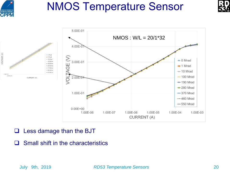
NMOS Temperature Sensor
Less damage than the BJT
Small shift in the characteristics
NMOS : W/L = 20/1*32