protection of upqc against the load side short circuits
TRANSCRIPT
Technological University Dublin Technological University Dublin
ARROW@TU Dublin ARROW@TU Dublin
Articles School of Electrical and Electronic Engineering
2010-01-01
Protection of UPQC Against the Load Side Short Circuits Protection of UPQC Against the Load Side Short Circuits
Iurie Axente Technological University Dublin
Malabika Basu Technological University Dublin, [email protected]
Michael Conlon Technological University Dublin, [email protected]
See next page for additional authors
Follow this and additional works at: https://arrow.tudublin.ie/engscheleart2
Part of the Electrical and Electronics Commons
Recommended Citation Recommended Citation Axente, I., Basu, M., Conlon, M., Gaughan, K.: Protection of UPQC Against the Load Side Short Circuits. IET Power Electronic, Vol.3, 4, pp.542-551. 2010. doi:10.1049/iet-pel.2009.0111
This Article is brought to you for free and open access by the School of Electrical and Electronic Engineering at ARROW@TU Dublin. It has been accepted for inclusion in Articles by an authorized administrator of ARROW@TU Dublin. For more information, please contact [email protected], [email protected].
This work is licensed under a Creative Commons Attribution-Noncommercial-Share Alike 4.0 License Funder: Enterprise Ireland

Authors Authors Iurie Axente, Malabika Basu, Michael Conlon, and Kevin Gaughan
This article is available at ARROW@TU Dublin: https://arrow.tudublin.ie/engscheleart2/38
Published in IET Power ElectronicsReceived on 5th March 2009Revised on 12th August 2009doi: 10.1049/iet-pel.2009.0111
ISSN 1755-4535
Protection of unified power qualityconditioner against the load side short circuitsI. Axente M. Basu M.F. Conlon K. GaughanSchool of Electrical Engineering Systems, Dublin Institute of Technology, Kevin Street, Dublin 8, IrelandE-mail: [email protected]
Abstract: This study presents a protection scheme for protecting the series inverter of a unified power qualityconditioner (UPQC). The proposed scheme protects the series inverter from overcurrents and overvoltages,which appear during short-circuit faults on the load side of the UPQC. The main protection element is acrowbar connected across the secondary of the series transformer and consists of a pair of antiparallelconnected thyristors, which is governed by a simple Zener diode-based control circuit. In the case of anovervoltage, the crowbar short circuits the secondary of the transformer, thus removing the overvoltage anddiverting the fault current from the series inverter. An additional circuit is used to disable the inverters inovercurrent conditions. The effectiveness of the proposed protection scheme is demonstrated both throughsimulation and experimentation.
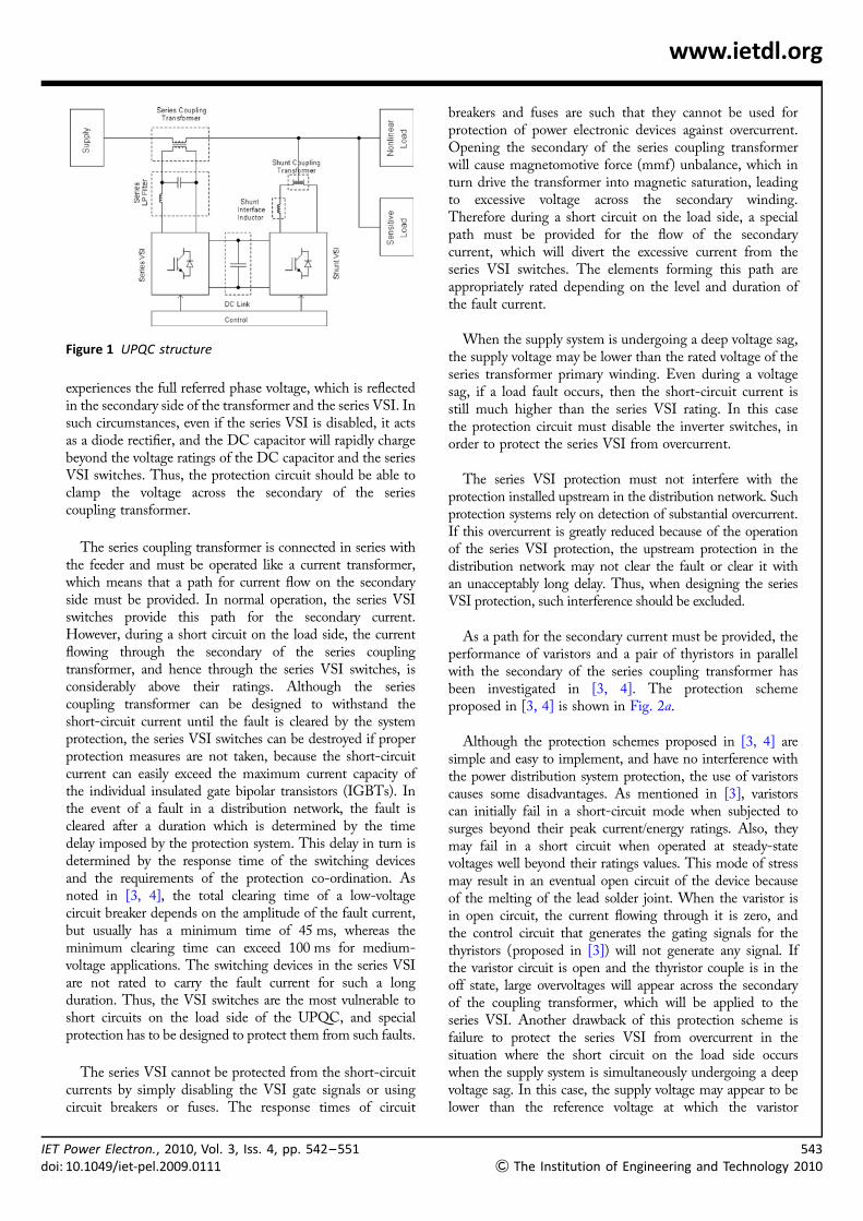
1 IntroductionThe unified power quality conditioner (UPQC) is a custompower device, which is expected to be one of the mostpowerful solutions for power quality improvement indistribution systems. It integrates series- and shunt-activepower filters, combining the operations of these two filterstogether [1, 2]. Fig. 1 shows a basic system configurationof a general UPQC.
On the DC side, the two filters are connected back-to-back sharing a common DC capacitor. The seriescomponent of the UPQC inserts an appropriate voltage tomaintain the voltage at the load terminals at a desired levelwhich is balanced and free of distortion (within the limitsprescribed by standards). This voltage is derived from avoltage source inverter (VSI) operated under pulse widthmodulation. Simultaneously, the shunt component of theUPQC injects current in the AC system such that thecurrents entering the bus to which the UPQC is connectedalso meet the required standards.
The series converter of the UPQC is connected in serieswith the electricity supply and this presents an imminentdanger to the series VSI when there is excessive currentflowing from the supply. Such a situation may arise because
of several reasons but primarily as a result of a short circuiton the load side. Before proceeding to explain theoperation of the proposed protection scheme, it is worthhighlighting the issues involved with a load side short circuit.
The series VSI is typically connected to the grid through alow-pass filter and a coupling transformer (see Fig. 1). Whena load side short circuit occurs, the voltage across the load isnearly zero, and almost all the supply voltage becomesproportionally distributed between the series couplingtransformer and the impedance of the supply system. Sincethe supply system impedance is much smaller than theimpedance introduced by the series compensator(consisting of the transformer impedance plus the referredimpedance of the series low-pass filter), a considerablybigger portion of the supply voltage drops across theprimary of the transformer. In the case of a stiff supply, itcan be considered that all the supply voltage is appliedacross the primary of the series coupling transformer.However, usually the rated voltage of the transformerprimary winding would not be greater than 50% of thesupply nominal voltage, when desired level of compensationis not more than 50% (as higher ratings may not beeconomically practical [2, p. 350] from power qualitydisturbance statistics). Thus, during the load side shortcircuit, the primary of the series coupling transformer
542 IET Power Electron., 2010, Vol. 3, Iss. 4, pp. 542–551
& The Institution of Engineering and Technology 2010 doi: 10.1049/iet-pel.2009.0111
www.ietdl.org
experiences the full referred phase voltage, which is reflectedin the secondary side of the transformer and the series VSI. Insuch circumstances, even if the series VSI is disabled, it actsas a diode rectifier, and the DC capacitor will rapidly chargebeyond the voltage ratings of the DC capacitor and the seriesVSI switches. Thus, the protection circuit should be able toclamp the voltage across the secondary of the seriescoupling transformer.
The series coupling transformer is connected in series withthe feeder and must be operated like a current transformer,which means that a path for current flow on the secondaryside must be provided. In normal operation, the series VSIswitches provide this path for the secondary current.However, during a short circuit on the load side, the currentflowing through the secondary of the series couplingtransformer, and hence through the series VSI switches, isconsiderably above their ratings. Although the seriescoupling transformer can be designed to withstand theshort-circuit current until the fault is cleared by the systemprotection, the series VSI switches can be destroyed if properprotection measures are not taken, because the short-circuitcurrent can easily exceed the maximum current capacity ofthe individual insulated gate bipolar transistors (IGBTs). Inthe event of a fault in a distribution network, the fault iscleared after a duration which is determined by the timedelay imposed by the protection system. This delay in turn isdetermined by the response time of the switching devicesand the requirements of the protection co-ordination. Asnoted in [3, 4], the total clearing time of a low-voltagecircuit breaker depends on the amplitude of the fault current,but usually has a minimum time of 45 ms, whereas theminimum clearing time can exceed 100 ms for medium-voltage applications. The switching devices in the series VSIare not rated to carry the fault current for such a longduration. Thus, the VSI switches are the most vulnerable toshort circuits on the load side of the UPQC, and specialprotection has to be designed to protect them from such faults.
The series VSI cannot be protected from the short-circuitcurrents by simply disabling the VSI gate signals or usingcircuit breakers or fuses. The response times of circuit
breakers and fuses are such that they cannot be used forprotection of power electronic devices against overcurrent.Opening the secondary of the series coupling transformerwill cause magnetomotive force (mmf) unbalance, which inturn drive the transformer into magnetic saturation, leadingto excessive voltage across the secondary winding.Therefore during a short circuit on the load side, a specialpath must be provided for the flow of the secondarycurrent, which will divert the excessive current from theseries VSI switches. The elements forming this path areappropriately rated depending on the level and duration ofthe fault current.
When the supply system is undergoing a deep voltage sag,the supply voltage may be lower than the rated voltage of theseries transformer primary winding. Even during a voltagesag, if a load fault occurs, then the short-circuit current isstill much higher than the series VSI rating. In this casethe protection circuit must disable the inverter switches, inorder to protect the series VSI from overcurrent.
The series VSI protection must not interfere with theprotection installed upstream in the distribution network. Suchprotection systems rely on detection of substantial overcurrent.If this overcurrent is greatly reduced because of the operationof the series VSI protection, the upstream protection in thedistribution network may not clear the fault or clear it withan unacceptably long delay. Thus, when designing the seriesVSI protection, such interference should be excluded.
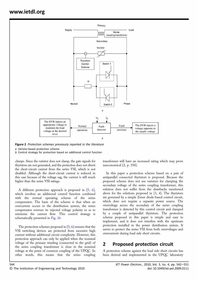
As a path for the secondary current must be provided, theperformance of varistors and a pair of thyristors in parallelwith the secondary of the series coupling transformer hasbeen investigated in [3, 4]. The protection schemeproposed in [3, 4] is shown in Fig. 2a.
Although the protection schemes proposed in [3, 4] aresimple and easy to implement, and have no interference withthe power distribution system protection, the use of varistorscauses some disadvantages. As mentioned in [3], varistorscan initially fail in a short-circuit mode when subjected tosurges beyond their peak current/energy ratings. Also, theymay fail in a short circuit when operated at steady-statevoltages well beyond their ratings values. This mode of stressmay result in an eventual open circuit of the device becauseof the melting of the lead solder joint. When the varistor isin open circuit, the current flowing through it is zero, andthe control circuit that generates the gating signals for thethyristors (proposed in [3]) will not generate any signal. Ifthe varistor circuit is open and the thyristor couple is in theoff state, large overvoltages will appear across the secondaryof the coupling transformer, which will be applied to theseries VSI. Another drawback of this protection scheme isfailure to protect the series VSI from overcurrent in thesituation where the short circuit on the load side occurswhen the supply system is simultaneously undergoing a deepvoltage sag. In this case, the supply voltage may appear to belower than the reference voltage at which the varistor
Figure 1 UPQC structure
IET Power Electron., 2010, Vol. 3, Iss. 4, pp. 542–551 543doi: 10.1049/iet-pel.2009.0111 & The Institution of Engineering and Technology 2010
www.ietdl.org
clamps. Since the varistor does not clamp, the gate signals forthyristors are not generated, and the protection does not divertthe short-circuit current from the series VSI, which is notdisabled. Although the short-circuit current is reduced inthis case because of the voltage sag, the current is still muchhigher than the series VSI ratings.
A different protection approach is proposed in [5, 6],which involves an additional control function combinedwith the normal operating scheme of the seriescompensator. The basis of the scheme is that when anovercurrent occurs in the distribution system, the seriescompensator reverses its injected voltage polarity so as tominimise the current flow. This control strategy isschematically presented in Fig. 2b.
The protection schemes proposed in [5, 6] ensures that theVSI switching devices are protected from excessive highcurrent without additional circuit complexity. However, thisprotection approach can only be applied when the nominalvoltage of the primary winding (connected to the grid) ofthe series coupling transformer is close to the nominalvoltage at the point of common coupling of the UPQC. Inother words, this means that the series coupling
transformer will have an increased rating which may proveuneconomical [2, p. 350].
In this paper a protection scheme based on a pair ofantiparallel connected thyristors is proposed. Because theproposed scheme does not use varistors for clamping thesecondary voltage of the series coupling transformer, thissolution does not suffer from the drawbacks mentionedabove for the solutions proposed in [3, 4]. The thyristorsare governed by a simple Zener diode-based control circuit,which does not require a separate power source. Theovervoltage across the secondary of the series couplingtransformer is detected by this control circuit and clampedby a couple of antiparallel thyristors. The protectionscheme proposed in this paper is simple and easy toimplement, and it does not interfere with the upstreamprotection installed in the power distribution system. Itserves to protect the series VSI from both overvoltages andovercurrents during load side short circuits.
2 Proposed protection circuitA protection scheme against the load side short circuits hasbeen derived and implemented in the UPQC laboratory
Figure 2 Protection schemes previously reported in the literature
a Varistor-based protection schemeb Control strategy for protection based on additional control function
544 IET Power Electron., 2010, Vol. 3, Iss. 4, pp. 542–551
& The Institution of Engineering and Technology 2010 doi: 10.1049/iet-pel.2009.0111
www.ietdl.org
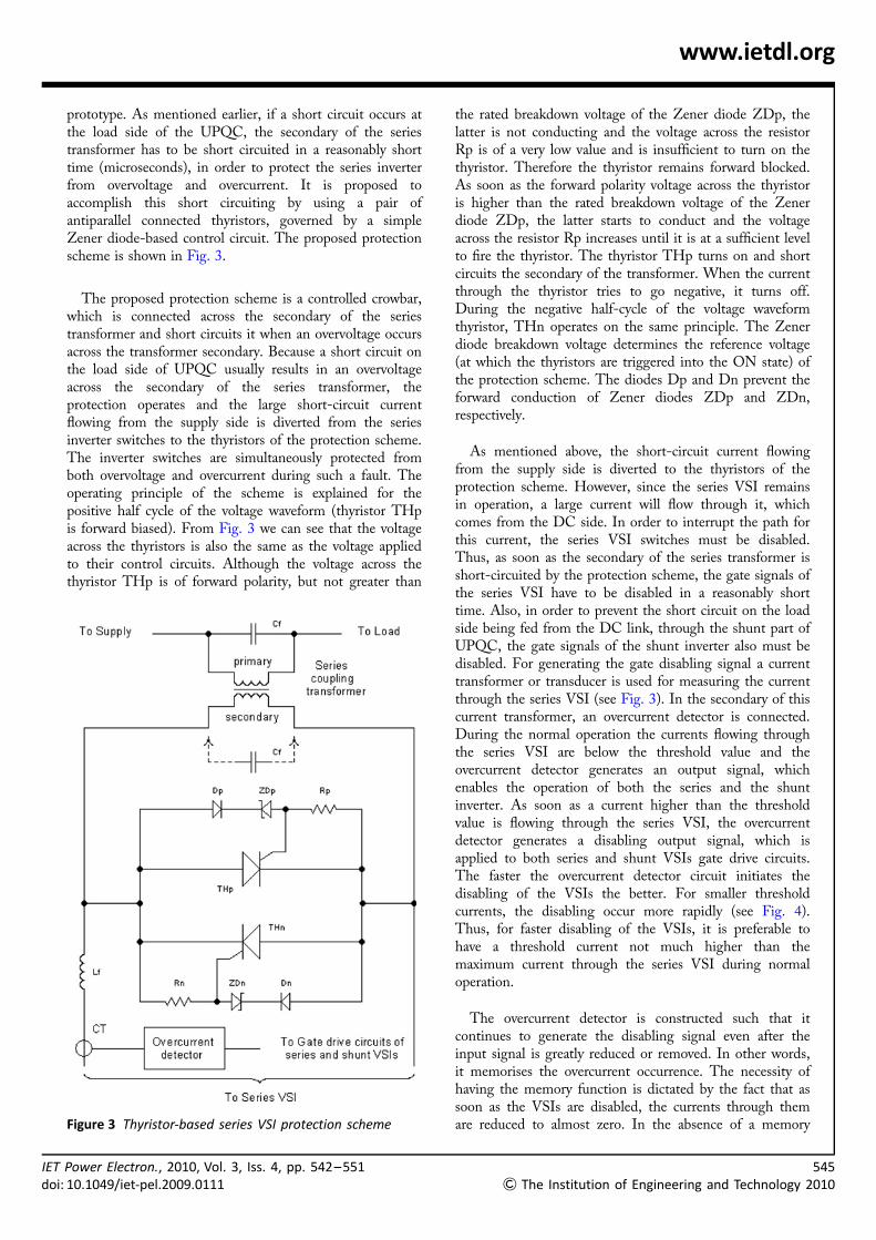
prototype. As mentioned earlier, if a short circuit occurs atthe load side of the UPQC, the secondary of the seriestransformer has to be short circuited in a reasonably shorttime (microseconds), in order to protect the series inverterfrom overvoltage and overcurrent. It is proposed toaccomplish this short circuiting by using a pair ofantiparallel connected thyristors, governed by a simpleZener diode-based control circuit. The proposed protectionscheme is shown in Fig. 3.
The proposed protection scheme is a controlled crowbar,which is connected across the secondary of the seriestransformer and short circuits it when an overvoltage occursacross the transformer secondary. Because a short circuit onthe load side of UPQC usually results in an overvoltageacross the secondary of the series transformer, theprotection operates and the large short-circuit currentflowing from the supply side is diverted from the seriesinverter switches to the thyristors of the protection scheme.The inverter switches are simultaneously protected fromboth overvoltage and overcurrent during such a fault. Theoperating principle of the scheme is explained for thepositive half cycle of the voltage waveform (thyristor THpis forward biased). From Fig. 3 we can see that the voltageacross the thyristors is also the same as the voltage appliedto their control circuits. Although the voltage across thethyristor THp is of forward polarity, but not greater than
the rated breakdown voltage of the Zener diode ZDp, thelatter is not conducting and the voltage across the resistorRp is of a very low value and is insufficient to turn on thethyristor. Therefore the thyristor remains forward blocked.As soon as the forward polarity voltage across the thyristoris higher than the rated breakdown voltage of the Zenerdiode ZDp, the latter starts to conduct and the voltageacross the resistor Rp increases until it is at a sufficient levelto fire the thyristor. The thyristor THp turns on and shortcircuits the secondary of the transformer. When the currentthrough the thyristor tries to go negative, it turns off.During the negative half-cycle of the voltage waveformthyristor, THn operates on the same principle. The Zenerdiode breakdown voltage determines the reference voltage(at which the thyristors are triggered into the ON state) ofthe protection scheme. The diodes Dp and Dn prevent theforward conduction of Zener diodes ZDp and ZDn,respectively.
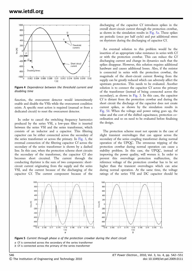
As mentioned above, the short-circuit current flowingfrom the supply side is diverted to the thyristors of theprotection scheme. However, since the series VSI remainsin operation, a large current will flow through it, whichcomes from the DC side. In order to interrupt the path forthis current, the series VSI switches must be disabled.Thus, as soon as the secondary of the series transformer isshort-circuited by the protection scheme, the gate signals ofthe series VSI have to be disabled in a reasonably shorttime. Also, in order to prevent the short circuit on the loadside being fed from the DC link, through the shunt part ofUPQC, the gate signals of the shunt inverter also must bedisabled. For generating the gate disabling signal a currenttransformer or transducer is used for measuring the currentthrough the series VSI (see Fig. 3). In the secondary of thiscurrent transformer, an overcurrent detector is connected.During the normal operation the currents flowing throughthe series VSI are below the threshold value and theovercurrent detector generates an output signal, whichenables the operation of both the series and the shuntinverter. As soon as a current higher than the thresholdvalue is flowing through the series VSI, the overcurrentdetector generates a disabling output signal, which isapplied to both series and shunt VSIs gate drive circuits.The faster the overcurrent detector circuit initiates thedisabling of the VSIs the better. For smaller thresholdcurrents, the disabling occur more rapidly (see Fig. 4).Thus, for faster disabling of the VSIs, it is preferable tohave a threshold current not much higher than themaximum current through the series VSI during normaloperation.
The overcurrent detector is constructed such that itcontinues to generate the disabling signal even after theinput signal is greatly reduced or removed. In other words,it memorises the overcurrent occurrence. The necessity ofhaving the memory function is dictated by the fact that assoon as the VSIs are disabled, the currents through themare reduced to almost zero. In the absence of a memoryFigure 3 Thyristor-based series VSI protection scheme
IET Power Electron., 2010, Vol. 3, Iss. 4, pp. 542–551 545doi: 10.1049/iet-pel.2009.0111 & The Institution of Engineering and Technology 2010
www.ietdl.org
function, the overcurrent detector would intermittentlyenable and disable the VSIs while the overcurrent conditionexists. A specific reset action is required (manual or from adedicated circuit) to reset the overcurrent detector.
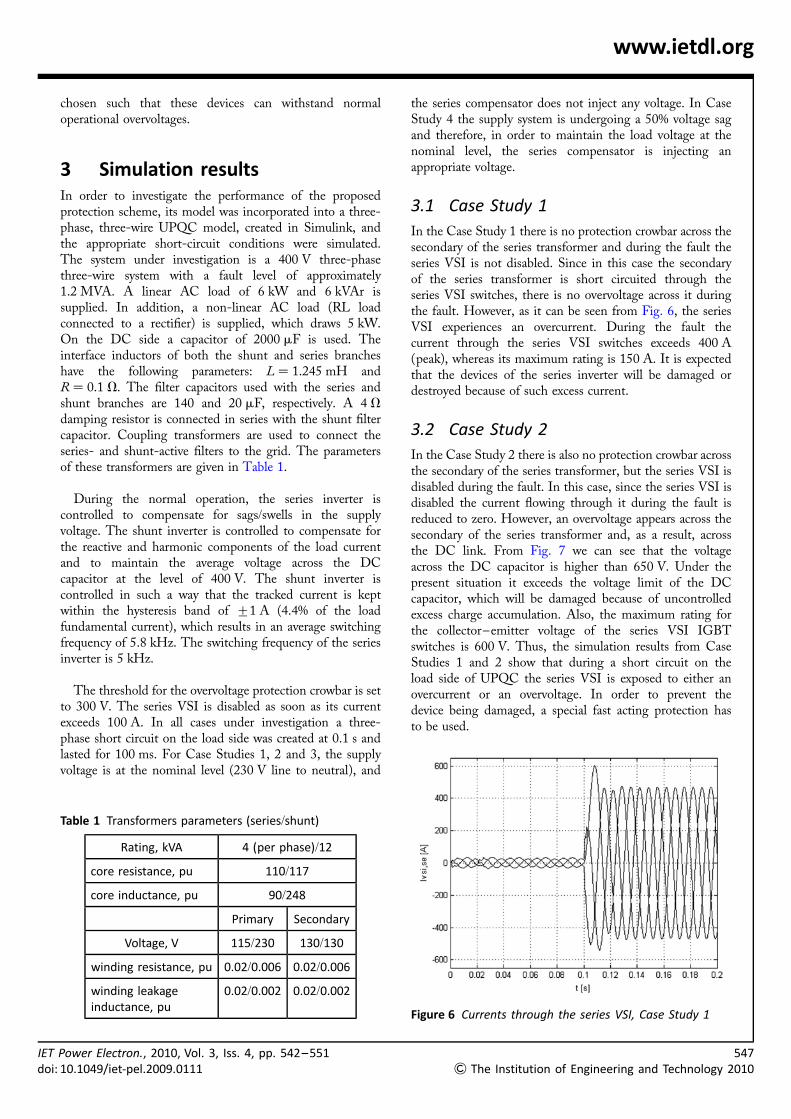
In order to cancel the switching frequency harmonicsproduced by the series VSI, a low-pass filter is insertedbetween the series VSI and the series transformer, whichconsists of an inductor and a capacitor. This filteringcapacitor can be either connected across the secondary ofthe series transformer or across the primary. In Fig. 3, theeventual connection of the filtering capacitor Cf across thesecondary of the series transformer is shown by a dashedline. In this case, when the protection scheme short circuitsthe secondary of the transformer, the capacitor Cf alsobecomes short circuited. The current through theconducting thyristor is the sum of two components: short-circuit current originating from the supply and the seriesVSI, and the current because of the discharging of thecapacitor Cf. The current component because of the
discharging of the capacitor Cf introduces spikes in theoverall short-circuit current through the protection crowbar,as shown in the simulation results in Fig. 5a. These spikesare periodic (once per half cycle) and put additional stresson thyristors during the discharging of capacitor Cf.
An eventual solution to this problem would be theinsertion of an appropriate value resistance in series with Cfor with the protection crowbar. This can reduce the Cfdischarging current and change its dynamics such that thespikes disappear. However, this solution requires additionalhardware and causes additional losses. Also, if the resistoris connected in series with the protection crowbar, themagnitude of the short-circuit current flowing from thesupply can be greatly reduced which can adversely affect theupstream protection. This needs to be evaluated. Anothersolution is to connect the capacitor Cf across the primaryof the transformer (instead of being connected across thesecondary), as shown in Fig. 3. In this case, the capacitorCf is distant from the protection crowbar and during theshort circuit the discharge of the capacitor does not createcurrent spikes, as shown by the simulation results inFig. 5b. When the voltage and power rating goes up, thevalue and the cost of the shifted capacitance, protection co-ordination and so on need to be evaluated before finalisingthe design.
The protection scheme must not operate in the case ofslight transient overvoltages that can appear across thesecondary of the series coupling transformer during normaloperation of the UPQC. The erroneous tripping of theprotection crowbar during normal operation can cause astability problem. In this case, the UPQC, instead ofimproving the power quality, will worsen it. In order toprevent this overvoltage protection malfunction, thereference voltage of the protection crowbar has to be sethigher than the transient overvoltages which can ariseduring normal operation. At the same time, the voltageratings of the series VSI and DC capacitor should be
Figure 5 Current through phase a of the protection crowbar during the short circuit
a Cf is connected across the secondary of the series transformerb Cf is connected across the primary of the series transformer
Figure 4 Dependence between the threshold current anddisabling time
546 IET Power Electron., 2010, Vol. 3, Iss. 4, pp. 542–551
& The Institution of Engineering and Technology 2010 doi: 10.1049/iet-pel.2009.0111
www.ietdl.org
chosen such that these devices can withstand normaloperational overvoltages.
3 Simulation resultsIn order to investigate the performance of the proposedprotection scheme, its model was incorporated into a three-phase, three-wire UPQC model, created in Simulink, andthe appropriate short-circuit conditions were simulated.The system under investigation is a 400 V three-phasethree-wire system with a fault level of approximately1.2 MVA. A linear AC load of 6 kW and 6 kVAr issupplied. In addition, a non-linear AC load (RL loadconnected to a rectifier) is supplied, which draws 5 kW.On the DC side a capacitor of 2000 mF is used. Theinterface inductors of both the shunt and series brancheshave the following parameters: L ¼ 1.245 mH andR ¼ 0.1 V. The filter capacitors used with the series andshunt branches are 140 and 20 mF, respectively. A 4 V
damping resistor is connected in series with the shunt filtercapacitor. Coupling transformers are used to connect theseries- and shunt-active filters to the grid. The parametersof these transformers are given in Table 1.
During the normal operation, the series inverter iscontrolled to compensate for sags/swells in the supplyvoltage. The shunt inverter is controlled to compensate forthe reactive and harmonic components of the load currentand to maintain the average voltage across the DCcapacitor at the level of 400 V. The shunt inverter iscontrolled in such a way that the tracked current is keptwithin the hysteresis band of +1 A (4.4% of the loadfundamental current), which results in an average switchingfrequency of 5.8 kHz. The switching frequency of the seriesinverter is 5 kHz.
The threshold for the overvoltage protection crowbar is setto 300 V. The series VSI is disabled as soon as its currentexceeds 100 A. In all cases under investigation a three-phase short circuit on the load side was created at 0.1 s andlasted for 100 ms. For Case Studies 1, 2 and 3, the supplyvoltage is at the nominal level (230 V line to neutral), and
the series compensator does not inject any voltage. In CaseStudy 4 the supply system is undergoing a 50% voltage sagand therefore, in order to maintain the load voltage at thenominal level, the series compensator is injecting anappropriate voltage.
3.1 Case Study 1
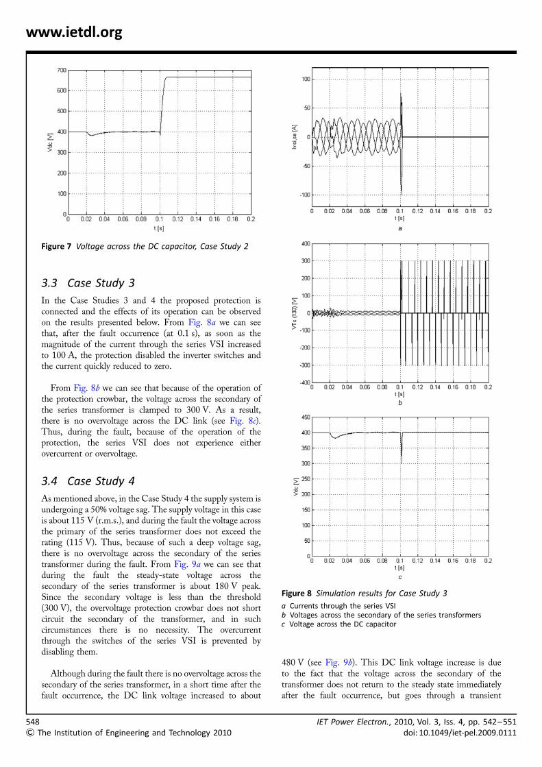
In the Case Study 1 there is no protection crowbar across thesecondary of the series transformer and during the fault theseries VSI is not disabled. Since in this case the secondaryof the series transformer is short circuited through theseries VSI switches, there is no overvoltage across it duringthe fault. However, as it can be seen from Fig. 6, the seriesVSI experiences an overcurrent. During the fault thecurrent through the series VSI switches exceeds 400 A(peak), whereas its maximum rating is 150 A. It is expectedthat the devices of the series inverter will be damaged ordestroyed because of such excess current.
3.2 Case Study 2
In the Case Study 2 there is also no protection crowbar acrossthe secondary of the series transformer, but the series VSI isdisabled during the fault. In this case, since the series VSI isdisabled the current flowing through it during the fault isreduced to zero. However, an overvoltage appears across thesecondary of the series transformer and, as a result, acrossthe DC link. From Fig. 7 we can see that the voltageacross the DC capacitor is higher than 650 V. Under thepresent situation it exceeds the voltage limit of the DCcapacitor, which will be damaged because of uncontrolledexcess charge accumulation. Also, the maximum rating forthe collector–emitter voltage of the series VSI IGBTswitches is 600 V. Thus, the simulation results from CaseStudies 1 and 2 show that during a short circuit on theload side of UPQC the series VSI is exposed to either anovercurrent or an overvoltage. In order to prevent thedevice being damaged, a special fast acting protection hasto be used.
Table 1 Transformers parameters (series/shunt)
Rating, kVA 4 (per phase)/12
core resistance, pu 110/117
core inductance, pu 90/248
Primary Secondary
Voltage, V 115/230 130/130
winding resistance, pu 0.02/0.006 0.02/0.006
winding leakageinductance, pu
0.02/0.002 0.02/0.002
Figure 6 Currents through the series VSI, Case Study 1
IET Power Electron., 2010, Vol. 3, Iss. 4, pp. 542–551 547doi: 10.1049/iet-pel.2009.0111 & The Institution of Engineering and Technology 2010
www.ietdl.org
3.3 Case Study 3
In the Case Studies 3 and 4 the proposed protection isconnected and the effects of its operation can be observedon the results presented below. From Fig. 8a we can seethat, after the fault occurrence (at 0.1 s), as soon as themagnitude of the current through the series VSI increasedto 100 A, the protection disabled the inverter switches andthe current quickly reduced to zero.
From Fig. 8b we can see that because of the operation ofthe protection crowbar, the voltage across the secondary ofthe series transformer is clamped to 300 V. As a result,there is no overvoltage across the DC link (see Fig. 8c).Thus, during the fault, because of the operation of theprotection, the series VSI does not experience eitherovercurrent or overvoltage.
3.4 Case Study 4
As mentioned above, in the Case Study 4 the supply system isundergoing a 50% voltage sag. The supply voltage in this caseis about 115 V (r.m.s.), and during the fault the voltage acrossthe primary of the series transformer does not exceed therating (115 V). Thus, because of such a deep voltage sag,there is no overvoltage across the secondary of the seriestransformer during the fault. From Fig. 9a we can see thatduring the fault the steady-state voltage across thesecondary of the series transformer is about 180 V peak.Since the secondary voltage is less than the threshold(300 V), the overvoltage protection crowbar does not shortcircuit the secondary of the transformer, and in suchcircumstances there is no necessity. The overcurrentthrough the switches of the series VSI is prevented bydisabling them.
Although during the fault there is no overvoltage across thesecondary of the series transformer, in a short time after thefault occurrence, the DC link voltage increased to about
480 V (see Fig. 9b). This DC link voltage increase is dueto the fact that the voltage across the secondary of thetransformer does not return to the steady state immediatelyafter the fault occurrence, but goes through a transient
Figure 7 Voltage across the DC capacitor, Case Study 2
Figure 8 Simulation results for Case Study 3
a Currents through the series VSIb Voltages across the secondary of the series transformersc Voltage across the DC capacitor
548 IET Power Electron., 2010, Vol. 3, Iss. 4, pp. 542–551
& The Institution of Engineering and Technology 2010 doi: 10.1049/iet-pel.2009.0111
www.ietdl.org
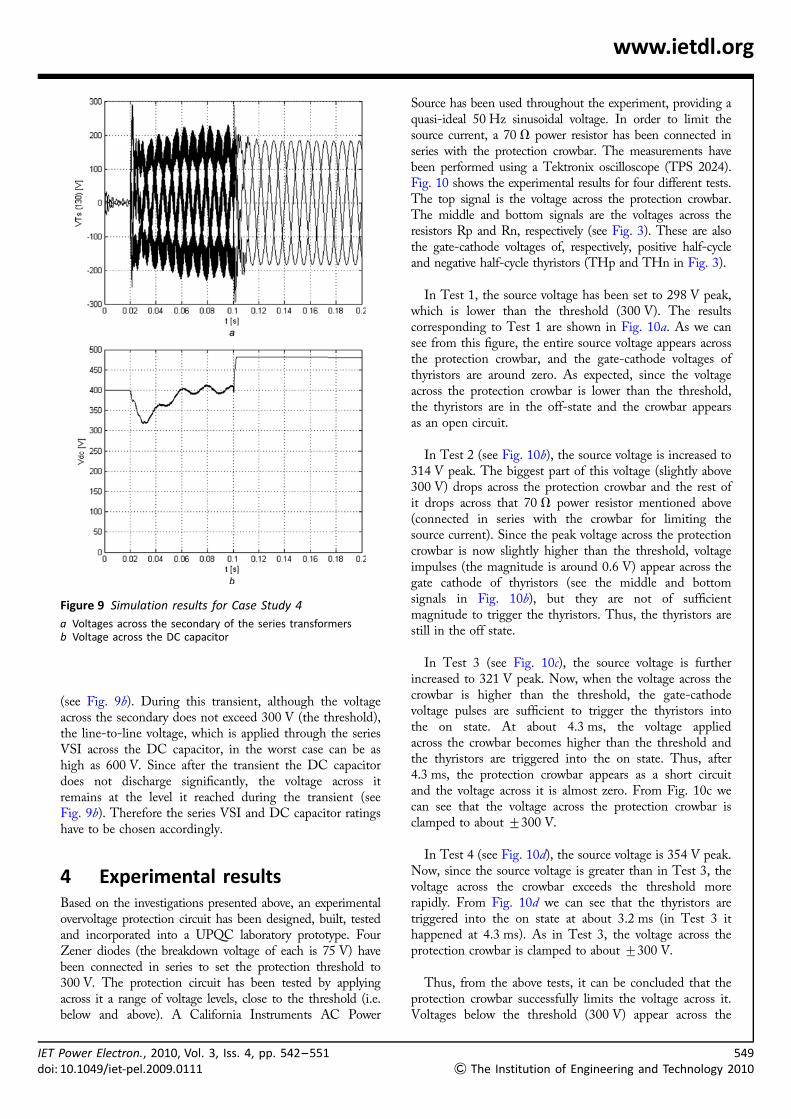
(see Fig. 9b). During this transient, although the voltageacross the secondary does not exceed 300 V (the threshold),the line-to-line voltage, which is applied through the seriesVSI across the DC capacitor, in the worst case can be ashigh as 600 V. Since after the transient the DC capacitordoes not discharge significantly, the voltage across itremains at the level it reached during the transient (seeFig. 9b). Therefore the series VSI and DC capacitor ratingshave to be chosen accordingly.
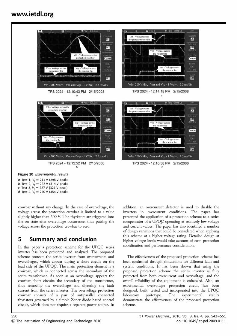
4 Experimental resultsBased on the investigations presented above, an experimentalovervoltage protection circuit has been designed, built, testedand incorporated into a UPQC laboratory prototype. FourZener diodes (the breakdown voltage of each is 75 V) havebeen connected in series to set the protection threshold to300 V. The protection circuit has been tested by applyingacross it a range of voltage levels, close to the threshold (i.e.below and above). A California Instruments AC Power
Source has been used throughout the experiment, providing aquasi-ideal 50 Hz sinusoidal voltage. In order to limit thesource current, a 70 V power resistor has been connected inseries with the protection crowbar. The measurements havebeen performed using a Tektronix oscilloscope (TPS 2024).Fig. 10 shows the experimental results for four different tests.The top signal is the voltage across the protection crowbar.The middle and bottom signals are the voltages across theresistors Rp and Rn, respectively (see Fig. 3). These are alsothe gate-cathode voltages of, respectively, positive half-cycleand negative half-cycle thyristors (THp and THn in Fig. 3).
In Test 1, the source voltage has been set to 298 V peak,which is lower than the threshold (300 V). The resultscorresponding to Test 1 are shown in Fig. 10a. As we cansee from this figure, the entire source voltage appears acrossthe protection crowbar, and the gate-cathode voltages ofthyristors are around zero. As expected, since the voltageacross the protection crowbar is lower than the threshold,the thyristors are in the off-state and the crowbar appearsas an open circuit.
In Test 2 (see Fig. 10b), the source voltage is increased to314 V peak. The biggest part of this voltage (slightly above300 V) drops across the protection crowbar and the rest ofit drops across that 70 V power resistor mentioned above(connected in series with the crowbar for limiting thesource current). Since the peak voltage across the protectioncrowbar is now slightly higher than the threshold, voltageimpulses (the magnitude is around 0.6 V) appear across thegate cathode of thyristors (see the middle and bottomsignals in Fig. 10b), but they are not of sufficientmagnitude to trigger the thyristors. Thus, the thyristors arestill in the off state.
In Test 3 (see Fig. 10c), the source voltage is furtherincreased to 321 V peak. Now, when the voltage across thecrowbar is higher than the threshold, the gate-cathodevoltage pulses are sufficient to trigger the thyristors intothe on state. At about 4.3 ms, the voltage appliedacross the crowbar becomes higher than the threshold andthe thyristors are triggered into the on state. Thus, after4.3 ms, the protection crowbar appears as a short circuitand the voltage across it is almost zero. From Fig. 10c wecan see that the voltage across the protection crowbar isclamped to about +300 V.
In Test 4 (see Fig. 10d), the source voltage is 354 V peak.Now, since the source voltage is greater than in Test 3, thevoltage across the crowbar exceeds the threshold morerapidly. From Fig. 10d we can see that the thyristors aretriggered into the on state at about 3.2 ms (in Test 3 ithappened at 4.3 ms). As in Test 3, the voltage across theprotection crowbar is clamped to about +300 V.
Thus, from the above tests, it can be concluded that theprotection crowbar successfully limits the voltage across it.Voltages below the threshold (300 V) appear across the
Figure 9 Simulation results for Case Study 4
a Voltages across the secondary of the series transformersb Voltage across the DC capacitor
IET Power Electron., 2010, Vol. 3, Iss. 4, pp. 542–551 549doi: 10.1049/iet-pel.2009.0111 & The Institution of Engineering and Technology 2010
www.ietdl.org
crowbar without any change. In the case of overvoltage, thevoltage across the protection crowbar is limited to a valueslightly higher than 300 V. The thyristors are triggered intothe on state after overvoltage occurrence, thus putting thevoltage across the protection crowbar to zero.
5 Summary and conclusionIn this paper a protection scheme for the UPQC seriesinverter has been presented and analysed. The proposedscheme protects the series inverter from overcurrents andovervoltages, which appear during a short circuit on theload side of the UPQC. The main protection element is acrowbar, which is connected across the secondary of theseries transformer. As soon as an overvoltage appears thecrowbar short circuits the secondary of the transformer,thus removing the overvoltage and diverting the faultcurrent from the series inverter. The overvoltage protectioncrowbar consists of a pair of antiparallel connectedthyristors governed by a simple Zener diode-based controlcircuit, which does not require a separate power source. In
addition, an overcurrent detector is used to disable theinverters in overcurrent conditions. The paper haspresented the application of a protection scheme to a seriescompensator of a UPQC operating at relatively low voltageand current values. The paper has also identified a numberof design variations that could be considered when applyingthis scheme at a higher voltage rating. Detailed design athigher voltage levels would take account of cost, protectioncoordination and performance consideration.
The effectiveness of the proposed protection scheme hasbeen confirmed through simulations for different fault andsystem conditions. It has been shown that using theproposed protection scheme the series inverter is fullyprotected from both overcurrent and overvoltage, and theoverall reliability of the equipment is enhanced. Also, anexperimental overvoltage protection circuit has beendesigned, built, tested and incorporated into the UPQClaboratory prototype. The experimental resultsdemonstrate the effectiveness of the proposed protectionscheme.
Figure 10 Experimental results
a Test 1, Vs ¼ 211 V (298 V peak)b Test 2, Vs ¼ 222 V (314 V peak)c Test 3, Vs ¼ 227 V (321 V peak)d Test 4, Vs ¼ 250 V (354 V peak)
550 IET Power Electron., 2010, Vol. 3, Iss. 4, pp. 542–551
& The Institution of Engineering and Technology 2010 doi: 10.1049/iet-pel.2009.0111
www.ietdl.org
6 AcknowledgmentsThe authors gratefully acknowledge Enterprise Ireland fortheir sponsorship of the Unified Power Quality Conditionerproject.
7 References
[1] FUJITA H., AKAGI H.: ‘The unified power quality conditioner:the integration of series- and shunt-active filters’, IEEE Trans.Power Electron., 1998, 13, (2), pp. 315–322
[2] GHOSH A., LEDWICH G.: ‘Power quality enhancement usingcustom power devices’ (Kluwer Academic Publishers,Boston, 2002)
[3] MORAN L.A., PASTORINI I., DIXON J., WALLACE R.: ‘Afault protection scheme for series active power filters’,IEEE Trans. Power Electron., 1999, 14, (5), pp. 928–938
[4] NEWMAN M.J., HOLMES D.G.: ‘An integrated approach forthe protection of series injection inverters’. IndustryApplications Conf., 2001, vol. 2, pp. 871–878
[5] LEE W.-C., LEE T.-K., MA C.-S., HYUN D.-S.: ‘A fault protectionscheme for series active compensators’. Power ElectronicsSpecialists Conf., 2002, vol. 3, pp. 1217–1222
[6] CHOI S.S., WANG T.X., MAHINDA VILATHGAMUWA D.: ‘A seriescompensator with fault current limiting function’, IEEETrans. Power Deliv., 2005, 20, (3), pp. 2248–2256
IET Power Electron., 2010, Vol. 3, Iss. 4, pp. 542–551 551doi: 10.1049/iet-pel.2009.0111 & The Institution of Engineering and Technology 2010
www.ietdl.org