non-destructive optical techniques for the...
TRANSCRIPT
Non-Destructive Optical Techniques for the Detection of Defects and
Stress in Sapphire
Ikerionwu A. Akwani, Douglas L. Hibbard, Keith T. Jacoby
Exotic Electro-Optics (EEO), 36570 Briggs Road Murrieta, California, 92563
Abstract
Because of its high strength and wide practical wavelength range, sapphire has become the
material of choice for large aperture windscreens for a number of electro-optical system
applications. Surface stress, sub-surface damage and bulk stress introduced during crystal growth
and optical fabrication can each deleteriously effect critical opto-mechanical performance
characteristics in windows such as strength and durability. Traditional methods for measuring
these defects are destructive and, therefore, unsuitable as in-process inspection tools for actual
flight hardware. Several non-destructive optical techniques are presently under investigation at
Exotic Electro-Optics under funding by the Air Force Research Laboratory. These include
polarization-based methods. An update on experimental results using the photoelasticity
technique, a modified circular polariscope, will be presented. The ultimate goal of this research
program is to provide a better understanding of the overall manufacturing process leading to the
optimal fabrication process parameters, time and cost.
1.0 Introduction
Crystal growth and optical fabrication processes such as grinding and polishing operations lead to
the creation of surface and sub-surface damage. These defects degrade the strength and the
performance of functional materials. In order to optimize thermo-mechanical performance, the
damaged layer must be identified and minimized or eliminated by subsequent process steps.
Traditional testing methods for measuring surface stress and sub-surface damage include ball
indention testing, cleaving and cross-sectional analysis, and wedge-polish-etch testing, which are
all destructive tests [1, 2, 3]. The basic goal of this study is to identify and develop a method
capable of detecting and quantifying defects, stress and sub-surface damage using a non-
destructive approach. More specifically, this work is focused on a polarization-based method
(photoelasticity) that appeared to be the most applicable as a large sapphire panel stress and
defect mapping tool.
To evaluate the application of this non-contact technique to the detection of defects and stress
fields inherent or applied to sapphire panels, a set of a-plane sapphire panels were characterized.
The sample set was composed of a number of polished specimens. The stress fields occurring in a
sapphire crystal panel are caused by the distortion of the crystal lattice. Our objective in this set of
experiments was two-fold: (a) to use a modified polariscope to detect defects in sapphire panels
and (b) to investigate the stress pattern/distribution associated with applied loads and begin to
quantify those effects.
2.0 Optical birefringence (retardation)
Optical polarization based methods are well established means of characterizing materials. In this
case, the technique involves measuring the relative retardance of two orthogonal linearly
polarized light rays (ne and no are the refractive indices of the extraordinary and ordinary rays) as
they pass through a sapphire panel. The beam emerging from the panel is transformed into
circular, elliptical or linear polarization state depending on the value of the induced phase shift.
The index of refraction of the ne ray varies with the direction of light propagation as follows:
(1)
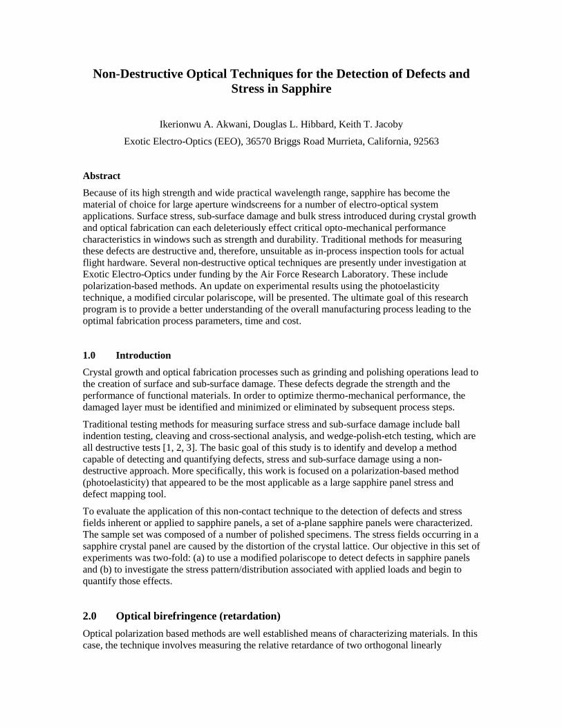
where θ is the angle between direction of the beam and the optical axis. Birefringence, (ne –n0),
will be maximum when the extraordinary ray is perpendicular to the optical axis. This yields the
highest degree of interference coloration. Figure 1 shows the index surface of an optically
uniaxial crystal for a positive and negative crystal.
Figure 1. (a) and (b) index surface of an optically uniaxial crystal where Q is the angle between direction of
the beam and the optical axis.
Birefringence is also sensitive to the stress state of the material. As such, the measured level of
birefringence can be used to quantify stress in the panel. The relationship between retardance and
birefringence is given by
retardation = )( oe nnh (2)
and the corresponding phase difference is
)(
2
0
oe nnh
(3)
where h is the thickness of the sapphire panel in nanometers and 0 is the vacuum wavelength.
The phase difference or relative retardation, , of the emergent beams is related to the
principal-stress difference, )( 21 , using the Stress-Optic law, as follows:
)(2
21hc
(4)
)}sin()cos({ 22
0
22)(
0
nn
nnn
e
ee
where l is the wavelength of light used and c is the direct stress-optic coefficient. The relative
retardation changes from point to point depending on the degree of stress. Therefore, the intensity
of light transmitted is governed by the stress fields. The relationship between the transmitted light
intensity and relative retardation, , or principal stress difference, )( 21 , for a circular
polariscope is given as:
2
sin 2
0II (for dark-field) (5)
2
cos2
0II (for bright-field) (6)
where I and I0 are the output intensity and incident intensity, respectively. It is convenient to
express equation (4) as
h
Kf21 (N/m
2) (7)
where K is the relative retardation in terms of a complete cycle of retardation,
2
K (8)
and C
f (9)
is the material fringe value. For a given material fringe value, f , and relative retardation, K ,
the principal-stress difference ( 21 ) can be determined at every point. Practically, K (the
measured fringe order) is determined with a polariscope and f is established by calibration
techniques.
By using appropriate combinations of wave-plates (quarter and half wave plates) and
coordinating their orientations with respect to the optical axis, any desired output polarization
state can be achieved. This provides the basis for applications to support material characterization
and product development.
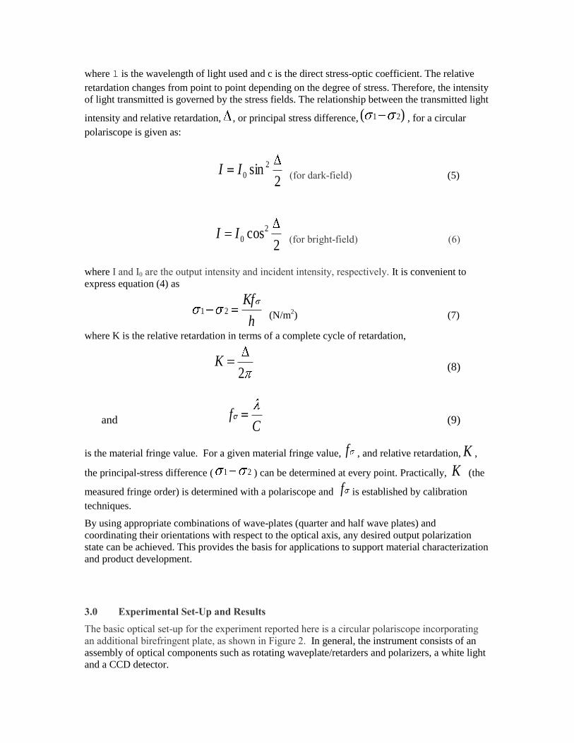
3.0 Experimental Set-Up and Results
The basic optical set-up for the experiment reported here is a circular polariscope incorporating
an additional birefringent plate, as shown in Figure 2. In general, the instrument consists of an
assembly of optical components such as rotating waveplate/retarders and polarizers, a white light
and a CCD detector.
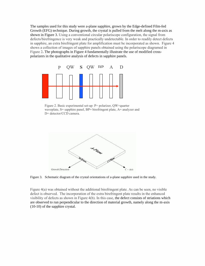
The samples used for this study were a-plane sapphire, grown by the Edge-defined Film-fed
Growth (EFG) technique. During growth, the crystal is pulled from the melt along the m-axis as
shown in Figure 3. Using a conventional circular polariscope configuration, the signal from
defects/birefringence is very weak and practically undetectable. In order to readily detect defects
in sapphire, an extra birefringent plate for amplification must be incorporated as shown. Figure 4
shows a collection of images of sapphire panels obtained using the polariscope diagramed in
Figure 2. The photographs in Figure 4 fundamentally illustrate the use of modified cross-
polarizers in the qualitative analysis of defects in sapphire panels.
Figure 3. Schematic diagram of the crystal orientations of a-plane sapphire used in the study.
Figure 4(a) was obtained without the additional birefringent plate. As can be seen, no visible
defect is observed. The incorporation of the extra birefringent plate results in the enhanced
visibility of defects as shown in Figure 4(b). In this case, the defect consists of striations which
are observed to run perpendicular to the direction of material growth, namely along the m-axis
(10-10) of the sapphire crystal.
Figure 2. Basic experimental set-up: P= polarizer, QW=quarter
waveplate, S= sapphire panel, BP= birefringent plate, A= analyzer and
D= detector/CCD camera.
P QW QW A S BP D

Figure 4. (a) Sapphire panel 1 without the additional plate exhibiting no sign of defects; (b) sapphire panel
1 with the extra plate now exhibiting growth-related striations; (c) sapphire panel 2 showing growth defects
and lattice distortions; (d) sapphire panel 3 showing growth defects and fringes associated with stress.
The observed defects are attributed to growth-induced inhomogeneities that may affect the
processing and end-application of the sapphire panel. Figure 4(c) exhibits growth defects in
addition to lattice distortion that are each clearly visible. This distortion is characterized by a
ridge-like structure that appears to split into two. Superimposed on this feature are small lines
running perpendicular to it. This particular feature has been observed previously in other sapphire
panels and it is attributed to the growth process. However, the origin of the ridge-like structure is
difficult to ascertain from the present study since no baseline data from the panel in the as-
received state were obtained prior to processing.
In Figure 4(d), growth defects and fringes associated with stress are observed. Since stress fields
in crystals change the electron density and the indices of refraction are mainly determined by
electron density, it follows that the observed striations and lattice distortions show varying indices
of refraction in different regions of the sapphire panel. Again, the detection of these defects is
improved by the extra birefringent plate.
Figure 5 shows the effect of analyzing beam direction versus the sapphire c-axis. In general, the
results show significant differences in defect visibility and interference colors. For example,
defects appear to be fainter and more colorful with increasing angle. For rotation angles of less
than 10 degrees, defects are more visible. Between 12 and 40 degrees, broad interference color
a b
c d
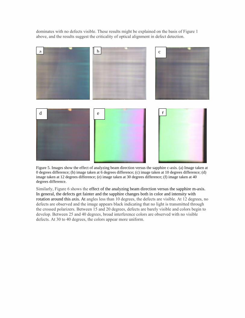
dominates with no defects visible. These results might be explained on the basis of Figure 1
above, and the results suggest the criticality of optical alignment in defect detection.
Figure 5. Images show the effect of analyzing beam direction versus the sapphire c-axis. (a) Image taken at
0 degrees difference; (b) image taken at 6 degrees difference; (c) image taken at 10 degrees difference; (d)
image taken at 12 degrees difference; (e) image taken at 30 degrees difference; (f) image taken at 40
degrees difference.
Similarly, Figure 6 shows the effect of the analyzing beam direction versus the sapphire m-axis.
In general, the defects get fainter and the sapphire changes both in color and intensity with
rotation around this axis. At angles less than 10 degrees, the defects are visible. At 12 degrees, no
defects are observed and the image appears black indicating that no light is transmitted through
the crossed polarizers. Between 15 and 20 degrees, defects are barely visible and colors begin to
develop. Between 25 and 40 degrees, broad interference colors are observed with no visible
defects. At 30 to 40 degrees, the colors appear more uniform.
a c
d e f
b

Figure 6. Images show the effect of analyzing beam direction versus the sapphire m-axis. (a) Image taken at
0 degrees difference; (b) image taken at 2 degrees difference; (c) image taken at 6 degrees difference; (d)
image taken at 10 degrees difference; (e) image taken at 12 degrees difference; (f) image taken at 15
degrees difference; (g) image taken at 20 degrees difference; (h) image taken at 25 degrees difference; (i)
image taken at 30 degrees difference; (j) image taken at 40 degrees difference.
a c
e f d
g h i
j
b

In Figure 7 the effect of polarization angle on defect detection is illustrated. Images were taken
for angles of 30, 70, 90 110 and 140 degrees between the polarizer and analyzer axes. It is clear
from the figure that defect visibility depends on the polarization direction. Defects appear fainter
with increasing polarization angle. At 140 degrees, defects become almost undetectable.
Figures 8 and 9 show the evolution of stress distribution in a sapphire panel with applied load.
Uniaxial stress was applied via a calibrated mechanical clamping mechanism along the m-
direction (Figure 9) and the c-direction (Figure 8). The spatial variation of the stress field was
obtained by imaging the light transmitted through the sample during the uniaxial compression.
From the figures, one can see significant differences in the images as a function of applied stress
and sample orientation. In general, mixed regions of dark and bright areas are clearly observed.
The color variation shows the signal strength and the bright areas indicate higher internal stress.
Figure 7. Images show the effect of polarization angle on defect detection. (a) Image taken at 30 degrees;
(b) image taken at 70 degrees; (c) image taken at 90 degrees; (d) image taken at 110 degrees; (e) image
taken at 140 degrees.
By comparing the image in the zero applied stress state and 5-pound stressed state, it is apparent
that the dark areas at zero applied stress become the bright areas in the stressed image and vise
versa. This change indicates a change in retardation value associated with the applied stress. The
change in phase difference over the same physical path length in sapphire is also increased as the
applied load is increased; hence, an increase in deformation corresponds to an increase in bright
areas. The bright areas are due to the stress-induced refractive index change which is related to
the phase shift by equation (3) above. Regions of highest induced local stress (stress
concentration points) are clearly visible (colored regions). As the applied load is increased, the
stress concentration points increase toward the center of the panel.
a b c
d e
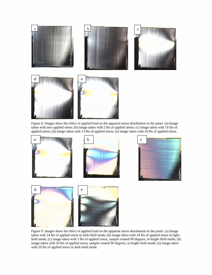
Figure 8. Images show the effect of applied load on the apparent stress distribution in the panel. (a) Image
taken with zero applied stress; (b) image taken with 5 lbs of applied stress; (c) image taken with 10 lbs of
applied stress; (d) image taken with 13 lbs of applied stress; (e) image taken with 19 lbs of applied stress.
Figure 9. Images show the effect of applied load on the apparent stress distribution in the panel. (a) Image
taken with 24 lbs of applied stress in dark-field mode; (b) image taken with 24 lbs of applied stress in light-
field mode; (c) image taken with 5 lbs of applied stress, sample rotated 90 degrees, in bright-field mode; (d)
image taken with 20 lbs of applied stress, sample rotated 90 degrees, in bright-field mode; (e) image taken
with 20 lbs of applied stress in dark-field mode.
a b c
d e
b c
d e
a
Existing material defects are strongly affected by the application of induced stress, as illustrated
by the brightness of the defect line (growth striation) in the dark-field mode in Figure 8 and
Figure 9(a). This type of defect may act as a stress amplifier, creating preferred sites for crack
initiation, resulting in overall strength degradation of the sapphire panel. Interestingly, this might
in part explain the variability in strength observed in sapphire panels. The observation of a stress
gradient across the panel suggests that atomic motion is parallel to the direction of uniaxial
compression. As the material is deformed, the material-light interactions change. The material’s
microscopic atomic rearrangement or behavior under applied stress leads to a change in the
macroscopic electric polarization of the material. The index of refraction varies with the
polarizability of the bonds in the material. The light intensity is a function of the index of
refraction which is in turn depends on the magnitude of the applied stress.
The representative stress distributions of four inspection-polished sapphire panels are shown in
Figure 12. This is the condition of panels as-received from the crystal growth vendor. This figure
clearly shows stress-induced multicolored regions in the sapphire panels. The observed
interference colors stem from the wavelength dependence of the retardation as described above. If
the retardance varies from one region to the next across the sapphire panel, the color of the light
transmitted will vary correspondingly. The observed colors represent varying stress levels. In
general, all four sapphire panels exhibit a similar characteristic stress pattern which includes a
saddle point close to the center of the panel. These saddle-shaped stress distributions are common
in photoelastic measurements. The stress/fringe pattern is not symmetric about the saddle point in
each case. The density of fringes throughout the sapphire panel indicates the degree of stress
variation. Comparison of the sapphire panels show that the exact shape of the saddle point and the
number of fringes in each panel is different, therefore indicating a different value of stress for
each panel. As the stresses increase, the fringe bands become narrower, denser and closely spaced
due to phase differences as described above in equation (4). This implies that the right of the
saddle point exhibits the highest stress value since it contains the greatest density of fringes,
followed by the left side, above and below the saddle point for Figure 12 (a), (b) and (c) while for
(d) the order of decreasing stress is right, above, left and below. In addition, a close examination
of Figure 12 (b), (c) and (d) reveals evidence of other defects as indicated by the arrows. These
results demonstrate the capability of the photoelastic technique to detect stresses and defects on
large sapphire panels very early in the fabrication process.
It is important to clarify that in order to quantitatively characterize stress in sapphire panels one
needs to determine the photoelastic constant, f (which is a material dependent quantity), and use
equation (7), as described.
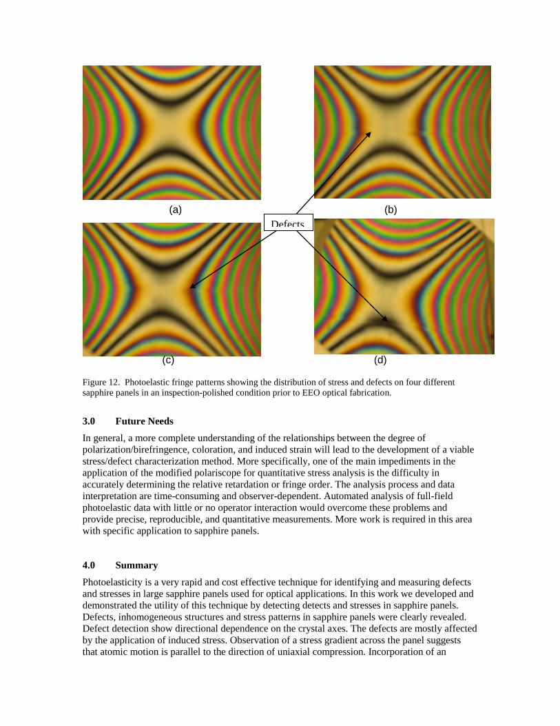
Figure 12. Photoelastic fringe patterns showing the distribution of stress and defects on four different
sapphire panels in an inspection-polished condition prior to EEO optical fabrication.
3.0 Future Needs
In general, a more complete understanding of the relationships between the degree of
polarization/birefringence, coloration, and induced strain will lead to the development of a viable
stress/defect characterization method. More specifically, one of the main impediments in the
application of the modified polariscope for quantitative stress analysis is the difficulty in
accurately determining the relative retardation or fringe order. The analysis process and data
interpretation are time-consuming and observer-dependent. Automated analysis of full-field
photoelastic data with little or no operator interaction would overcome these problems and
provide precise, reproducible, and quantitative measurements. More work is required in this area
with specific application to sapphire panels.
4.0 Summary
Photoelasticity is a very rapid and cost effective technique for identifying and measuring defects
and stresses in large sapphire panels used for optical applications. In this work we developed and
demonstrated the utility of this technique by detecting detects and stresses in sapphire panels.
Defects, inhomogeneous structures and stress patterns in sapphire panels were clearly revealed.
Defect detection show directional dependence on the crystal axes. The defects are mostly affected
by the application of induced stress. Observation of a stress gradient across the panel suggests
that atomic motion is parallel to the direction of uniaxial compression. Incorporation of an
(a) (b)
(c) (d)
Defects
additional birefringent plate in the conventional circular polariscope considerably improved the
sensitivity of defect detection. Qualitative analysis of stress concentration points and stress
regions and other defects associated with growth and fabrication operations can be identified
easily. The information can be used as an on-line check for sapphire quality inspection and
process improvement. This technique offers an excellent inspection capability for detection of a
wide variety of detect types, and has the potential to serve as a quantitative tool for characterizing
stress in sapphire panels. The fact that large panels can be characterized quickly in a single view
renders this method especially attractive as a simple shop-floor tool for revealing internal stresses.
Acknowledgement
This work was sponsored by the Office of the Naval Research (ONR) under Contract No.
N00014-04-C-0419, and Air Force Research Laboratory (AFRL) under Contracts No. FA 8650-
05-D-5806/0004 and No. FA 8650-06-5401/006.
References:
1. J.E. Greivenkamp, M. T. Chang, in Optical fabrication and testing workshop, 1992
Technical Digest Series, 24, (OSA, Washington, DC 1992).L. Grabner, J. Appl. Phys., 49
(2) 580-83 (1978).
2. D. Harris, Materials for Infrared Windows and Domes: Properties and Performance,
SPIE, Bellingham, WA, (1998).
3. Y. Zhou, P. D. Funkenbusch, D. J. Quesnel, D. Golini and A. Lindquist, J. Am. Ceram.
Soc. 77 (12) 3277-80 (1994).