nb3sn and related a15s 1 - national...
TRANSCRIPT

Nb3Sn and Related A15s
1
Chapter 11: Wires and Tapes
Chapter 11: Wires and Tapes .......................................................................................................... 1
11.3 History of Nb3Sn and Related A15 Wires .................................................................... 1
11.3.1 Introduction ............................................................................................................... 1
11.3.2 Chronological Progress in the Fabrication of Nb3Sn and V3Ga Wires ..................... 2
11.3.3 Bronze-processed Nb3Sn Wires ................................................................................ 7
11.3.4 Internal Sn-processed Nb3Sn Wires .......................................................................... 8
11.3.5 Conclusions and Future Outlook ............................................................................ 10
Further Reading ........................................................................................................................ 11
11.3 History of Nb3Sn and Related A15 Wires
Kyoji Tachikawa - Tokai University, Japan
Peter J. Lee – Florida State University, USA
11.3.1 Introduction
Nb3Sn occupies a special place in any history of superconductivity as the first material to
show, 50 years ago in 1961, that superconductivity actually could exist in very high fields. It is
both fitting and also perhaps remarkable that it so quickly made the transition from a Physical
Review Letter1 to high field magnets of 10 T or more that fulfilled Onnes’s 50-year-delayed
dreams. It was initially made as a few m thick layers in tape forms on strong substrates, so as to
allow application to magnets without performance being compromised by the hard and brittle
nature of its A15 crystal structure. However, the electromagnetic instabilities of superconducting
tapes were soon recognized. Following the development of filamentary forms of Nb-Ti in about
1965, the urge to develop a filamentary technology for A15 compounds occurred too. It was
soon discovered that the presence of a small amount of Cu enabled formation of the relevant A15
compound, V3Ga or Nb3Sn, at temperatures of 600-700 °C, some 200-300 °C below the
temperatures needed in the binary mixtures. Cu-Sn or Cu-Ga bronzes fulfilled this condition and
allowed fabrication of wires containing many hundreds or even thousands of Nb or V filaments
in the relevant bronze by conventional extrusion and drawing processes. This bronze route was
the breakthrough that enabled Nb3Sn multifilamentary conductor forms capable of producing
stable 10-23 T field magnets required for fusion, NMR, and all manner of other systems. Due to
these widespread applications, Nb3Sn can thus be regarded as one of the key materials in science
and technology. In this article the chronological progress of Nb3Sn wires will be surveyed,
together with some discussion of its brother A15 compound, V3Ga, which played an important
role too.
The A15 compounds, like Nb3Sn, have the nominal composition ratio of A3B, but although
1 J. E. Kunzler et al., Phys. Rev. Let. 6:3 (1961) 89

Nb3Sn and Related A15s
2
the stoichiometric A3B composition is obtained by diffusion, actually all possible compositions
that are stable also form, thus producing a range of superconducting properties. For technology it
is vital to work with at least ternary systems, since the formation temperature of Nb3Sn is
lowered from ~950 °C to ~700 °C by the addition of Cu. The constituent elements, Nb, Sn and
Cu, have a favorable workability at room temperature, allowing multifilamentary composites to
be assembled at larger size, co-drawn to final wire dimensions, and then reacted to form the A15
filament structure. Because optimum reaction conditions do not allow reaction to completion2,
the measured transition temperature Tc and upper critical field Bc2 of Nb3Sn wires have a width
that depends on the variable stoichiometry of the filaments. A central compromise of all
multifilamentary conductors is that grain boundaries provide the primary flux-pinning centers
requiring a low reaction temperature, while the highest Tc and Bc2 distribution requires a
somewhat higher reaction temperature that enlarges the grain size and reduces the flux pinning.
Third elements can also improve the performance of Nb3Sn wires and commercial strand
normally incorporates at least one of these. Most commonly, small amounts of Ti and Ta
addition are used to enhance the Bc2 by increasing the normal state resistivity of the A15 phase
which results in higher critical current density at fields above 12 T (4.2 K). Moreover the
addition of Ti appreciably accelerates the formation of Nb3Sn.
11.3.2 Chronological Progress in the Fabrication of Nb3Sn and V3Ga Wires
At the 1982 Applied Superconductivity Conference John Hulm recalled the circumstances
surrounded the discovery of superconductivity in the A15 compounds:3
"In the spring of 1952 I was working with a graduate student, George Hardy. We decided
that the carbides and nitrides were more or less exhausted, so we moved down to silicides
and germanides in the second and third periods. We also began arc-melting our samples.
These were two very fortunate moves. Not only was the general quality of the samples
improved over our earlier sintered materials, but we soon discovered a new high Tc super-
conductor, V3Si, at 17 K.4 It belonged to what was then known, erroneously, as the beta-
tungsten structure; of course this was subsequently changed to A15. I told this news to
Bernd Matthias almost immediately.
By then Bernd Matthias had teamed up with Ted Geballe, Ernie Corenzwit, and Sey-
mour Geller at the Bell Laboratories. These investigators proceeded to execute a tour-de-
force in creative synthesis by discovering about 30 new A15's, including several new high
Tc materials, most prominently Nb3Sn at 18 K, in 1954.5
On December 15th
1960, a group at Bell Laboratories led by J. E. Kunzler tested the high field
properties of a rectangular rod of bulk Nb3Sn, that had been sintered and then melted at 2400 °C and to their “complete surprise”
6, found that it was still superconducting at their maximum field
of 8.8 T. The details of the road to this discovery are covered in more detail in the ductile
superconductor history 11.2 but it should be repeated here that this achievement represented a
2 P. J. Lee and D. C. Larbalestier, Cryogenics, 48:7-8 (2008) 283
3 J. Hulm, IEEE Trans. on Magnets, 19:3 (1983) 161
4 George F. Hardy and John K. Hulm, Phys. Rev. 93:5 (1954) 1004
5 B. T. Matthias et al., Phys. Rev. 95:6 (1954) 1435
6 J. Kunzler, IEEE Trans. on Magnetics, 23:2 (1987) 396

Nb3Sn and Related A15s
3
prize of 21 bottles of scotch whisky courtesy of a wager with Morris Tanenbaum. The 2400 °C
bulk sample was impractical as the magnet material they had hoped to use for Masers. However,
“super technician” 7 Ernie Buehler (Tanenbaum and Buehler formed the team that made the first
Si transistor), devised the powder-in-tube (PIT) route to make wire, placing Sn and Nb powders
in a Nb tube, a ductile combination that could be drawn to final size before the reaction heat
treatment that would create the brittle Nb3Sn. The first strand carried 50 times higher Jc than the
bulk sample,1 and their best PIT strand (with 10% more Sn than was required to fully react the
Nb powder to the stoichiometric ratio) reached almost 1500 A/mm² at 8.8 T (4.2 K) using a
much more manageable heat treatment of 970 °C. Kunzler suggested that Nb3Sn wires might
enable a convenient and economical high-field magnet without the consumption of huge electric
power and cooling water required in a water-cooled Cu magnet.8
The next major milestone was the development of a vapor deposition technique to produce
Nb3Sn by J. J. Hanak (who became the father of Combinatorial Chemistry) at RCA Laborato-
ries.9 Chemical vapor deposition produced a thin enough layer of Nb3Sn on a wire or tape that
was flexible enough to wind magnets. Furthermore, the use of substrates with thermal expan-
sions greater than Nb3Sn placed the brittle A15 layer under beneficial compressive strain. The
technique involved production of gaseous NbCl4 and SnCl4 by direct reaction of Nb, Sn and Cl2.
The chlorides, together with H2 and HCl were passed into a reaction chamber in which a
continuously fed metallic substrate tape or wire was resistively heated between two carbon
electrodes to ~1000 °C.10
After growth of the Nb3Sn, layer of Ag was applied as the stabilizer.
Figure 11.3.1 illustrates the industrial CVD facilities developed for the winding of 10 T-class
superconducting magnets. A major effort was also underway at General Electric and in competi-
tion with RCA, they developed the
Nb3Sn diffusion process in which a Nb
substrate tape was passed through a
molten Sn bath.11
Nb3Sn layers were
formed on both sides of the tape after
the reaction heat treatment at 950 °C.
Stabilizing Cu layers were soldered to
the tape using the residual Sn left
behind after reaction, as shown in
Figure 11.3.2. Many 15 T-class
superconducting magnets, mostly used
for solid state physics research, were
wound from these tapes by Intermag-
netics General Co. (IGC), the spin-off
company that emerged from GE. Thus
the vision of Kunzler mentioned in ref.
7 Tanenbaum’s description of Ernie Buehler in “Oral-History: Goldey, Hittinger and Tanenbaum” interview
conducted by Michael Riordan and Sheldon Hochheiser, Murray Hill, New Jersey, September 25, 2008, Interview
#480 for the IEEE History Center, The Institute of Electrical and Electronics Engineers, Inc.. 8 J. Kunzler, Reviews of Modern Physics 33:4 (1961) 501
9 J. J. Hanak, "Vapor deposition of Nb3Sn," in Metallurgy of Advanced Electronic Materials, (AIME) 19, Ed. G. E.
Brock. (New York: Interscience, n.d.) (1963) 161 10
J. J Hanak, K. Strater, and G.W. Cullen, "Preparation and Properties of Vapor-Deposited Niobium Stannide",
RCA Review, September 1964 11
M.G. Benz, G.E. Research. & Development Center Report No. 66-C-044 (1966)
Figure 11.3.1: Production facilities for Nb3Sn wires
using the continuous CVD process were established at
RCA already in 1966 9.

Nb3Sn and Related A15s
4
8 was realized rather quickly. Nb3Sn
diffusion tape was also used for a
110 m-long power transmission model
cable operated at 7 K that was the
forerunner of the many electric utility
application dreams that flowered after
the discovery of superconductivity in
the cuprates in 1987.12
However, all tape magnets suffered
from flux jumps that made them slow to
charge and sometimes irregular in
performance. As monocore wires of Cu-
clad Nb-Zr gave way to better-bonded
Cu-Nb-Ti (see section 11.2) and then to
metallurgically bonded, twisted
multifilamentary Nb-Ti conductors,
superconducting magnets became
stable, capable of fast ramps and generally much more predictable. The drive to develop
multifilamentary A15 wires was on!
A key study in this transition from tapes to wires was made on V3Ga wires. A small Cu
addition to molten Ga was found to change the diffusion mode for growth of V3Ga from a grain
boundary one to a bulk one, without the Cu impairing the properties of the growing V3Ga layer.
Cu accumulated at the diffusion boundary, decreasing appreciably the formation temperature of
V3Ga as illustrated in Figure 11.3.3.13
The area fraction of V3Ga with fine grains is much
increased by the lower temperature reaction enabled by the Cu addition. The patent describing
the effect of Cu on the promotion of
V3Ga and Nb3Sn synthesis was filed in
1966.14
The V3Ga tape exhibits an
appreciably better performance than
pure Nb3Sn tape in fields above 15 T.
The 17.5 T superconducting magnet
system shown in Figure 11.3.4, which
held the field record for an all-
superconducting magnet for ~10 years
after 1975, was made by using a
Nb3Sn outer and a V3Ga inner
section.15
Only in the 1980’s was it
possible to exceed this performance
with multifilamentary conductors of
Nb3Sn with Ti addition.
The route to multifilamentary A15
conductors was greatly simplified by
12
E. Forsyth and G. Morgan, IEEE Trans. on Magnetics, 19:3 (1983) 652 13
K. Tachikawa and Y. Tanaka Japanese J. Applied Physics 6:6 (1967) 782 14
K. Tachikawa, Y. Tanaka and S. Fukuda, Japan Pat. 0670619 (Filed June 25, 1966) 15
K. Tachikawa et al., J. Cryogenic Soc. of Japan 11:6 (1976) 252
Figure 11.3.2: Nb3Sn tape produced at General
Electric using diffusion between a liquid Sn bath and a
Nb foil, later the basis of magnets made by Intermag-
netics General Corp.11
.
Figure 11.3.3: Formation of V3Ga layer by a diffusion
reaction between V and Ga. (a) diffusion at 800 °C
without Cu addition, and (b) at 700 °C with Cu
addition. The small dots represent the Cu in the Cu-Ga-
V ternary alloy.13

Nb3Sn and Related A15s
5
the work with Cu additions to V-Ga tapes,
and multifilamentary V3Ga wires were soon
fabricated using a Cu-Ga bronze matrix and
V cores.16
The first commercial multifila-
mentary V3Ga wire was produced by
Furukawa Electric in 1972 which was
wound into a stable 10.4 T magnet, and by
this time groups in Europe17
and the USA18
had also developed the bronze route to
make multifilamentary Nb3Sn wires.
Because bronze wires required many
anneals to allow wire drawing, interest
rapidly grew in modifications of the bronze
process, in which the more ductile pure
metal components of Sn, Cu and Nb were
used. The greatest longevity has come from
variants of the internal tin (IT) process, in
which a composite wire constructed from a Cu matrix, Sn and Nb cores (see Figure 11.3.5),
which was initiated by Mitsubishi Electric in 1974.19
Some of the earliest work on multifilamentary conductors using the bronze process was
performed at the UK Atomic Energy Research
Establishment at Harwell, where Nb3Sn tapes
were also found to produce too much electromag-
netic instability when in magnets. One of the
young researchers in the Harwell group, Phil
Charlesworth, recalls:20
It also soon became clear that the critical
problem in constructing superconducting
magnets is ensuring stability against
catastrophic quenching caused by small
movements of flux vortices rearranging
themselves against pinning sites during field
ramping. For this purpose, a wire containing
many thin filaments of superconductor
embedded in a normal conducting matrix of
low resistivity, providing dynamic stabilisa-
tion, is much more attractive than a tape, as
the filaments, if fine enough are adiabatically
stable and the matrix can help to damp out
propagation of fluctuations to neighbouring
16
K. Tachikawa, Proc. ICEC-3, Illife Sci. & Technol. Pub. (1970) 339 17
Brian Howlett, Great Britain Pat. 52,623/69 (Filed Oct. 27, 1969). US Pat. 3,728,165 (Filed Oct. 19, 1970) 18
A. R. Kaufman and J. J. Pickett, Bull. of American Phys. Soc. 15 (1970) 833 19
Y. Hashimoto, K. Yoshizaki and M. Tanaka, Proc. ICEC-5, K. Mendelssohn, Editor, (1974)332 20
Phil Charlesworth, personal communication for this article, October 17, 2010
Figure 11.3.4. 17.5 T superconducting magnet
system operated at the National Research Institute
for Metals.15
Figure 11.3.5: Schematic illustration of
bronze and internal Sn (IT) process.
Nb3Sn and Related A15s
6
filaments. Work along these lines was
started in Brian Howlett's group at
Harwell in 1969 with the progressive
development of the so-called bronze-
route, method of fabrication using
niobium rods embedded in copper-tin
bronze, the Nb3Sn being created by heat-
treatment to create a reaction layer
between the tin and the niobium. In early
1971, the group moved into Chemistry
Division with Jim Lee as group leader.
I was involved in this program to the
extent of measuring the properties of the
material produced but the bulk of the
effort went into development of a
production line for ever more sophisticat-
ed composites. The fabrication route
involved drilling a matrix of 37 holes in a
cylindrical bronze billet, using a gun
drill, inserting niobium rods and then
swaging and drawing the material to
bring the bronze into firm contact with
the niobium and to reduce the overall
diameter. The process could then be repeated, one or more times, using the previous
stage composites as inserts. Many people worked on this program but Derek Arm-
strong, who toured the country acquiring second-hand machine tools to build up the
industrial-scale fabrication shop we needed and threw himself with enthusiasm into
developing the fabrication route.
All along this work had been in collaboration with a team at the neighbouring Ruth-
erford Laboratory interested in producing practical solenoids with possible particle
accelerator applications in mind. Again there were several people involved but our
liaison was chiefly through David Larbalestier and Chris Scott. A joint paper in 1974 21
describes composites with filament counts up to 42,439 and including regions of pure
copper protected by a diffusion barrier to add extra stabilisation. Another paper of the
same date describes the successful performance of several small solenoids made from
our bronze-route material by winding the material as-fabricated and then heat-treating
the whole coil to produce the Nb3Sn.
It is interesting that Howlett’s bronze route patent was filed in 1969, and the work at
Brookhaven National Laboratory in the USA was clearly ongoing at this time too. Having efforts
in Japan, the UK and the USA led to competition that enormously enhanced progress. In
particular the joint Harwell-Rutherford program had led to intrinsically stable multifilamentary
conductors which had been wound into solenoid magnets generating more than 12 T in 1974.
21
D. Larbalestier et al., IEEE Trans. on Magnetics 11:2 (1975) 247 22
Courtesy of Osaka Alloying Works Co., Ltd. (2010)
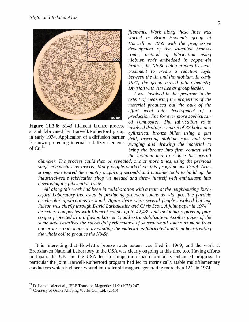
Figure 11.3.6: 5143 filament bronze process
strand fabricated by Harwell/Rutherford group
in early 1974. Application of a diffusion barrier
is shown protecting internal stabilizer elements
of Cu.21
Nb3Sn and Related A15s
7
11.3.3 Bronze-processed Nb3Sn Wires
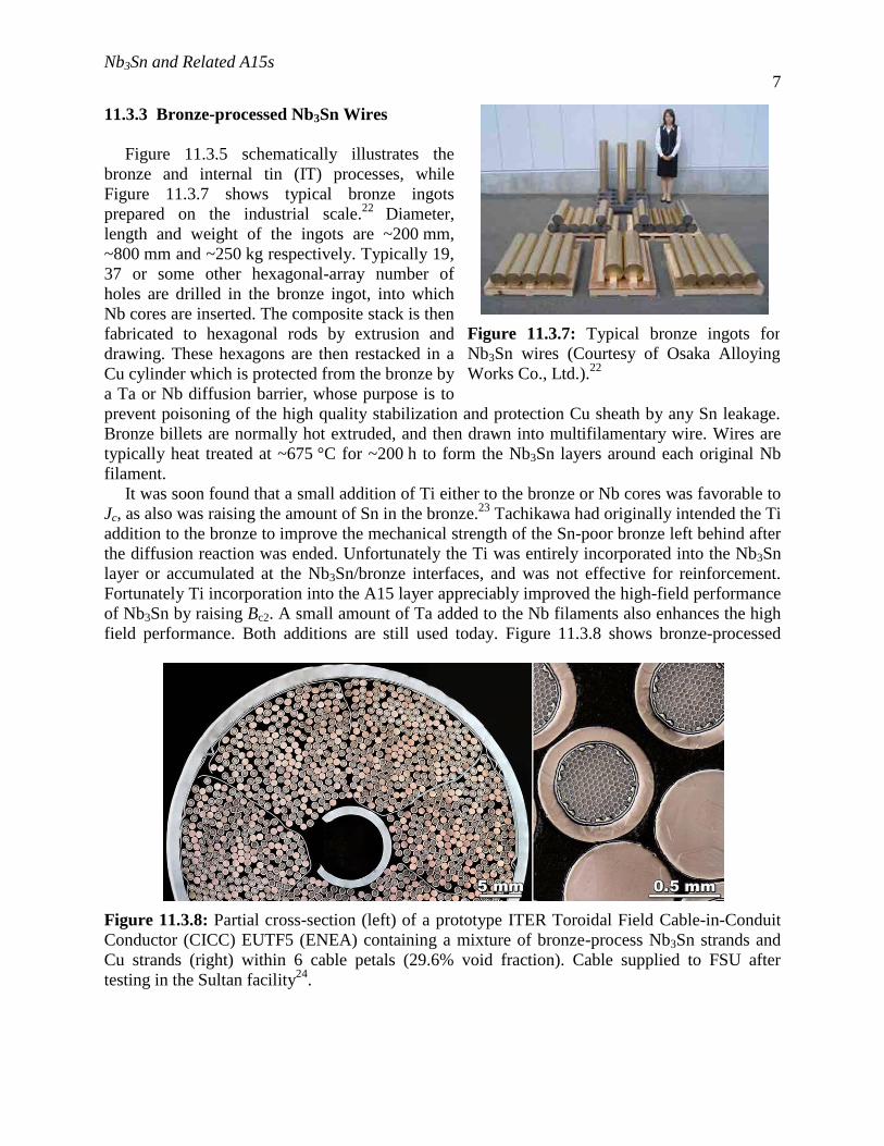
Figure 11.3.5 schematically illustrates the
bronze and internal tin (IT) processes, while
Figure 11.3.7 shows typical bronze ingots
prepared on the industrial scale.22
Diameter,
length and weight of the ingots are ~200 mm,
~800 mm and ~250 kg respectively. Typically 19,
37 or some other hexagonal-array number of
holes are drilled in the bronze ingot, into which
Nb cores are inserted. The composite stack is then
fabricated to hexagonal rods by extrusion and
drawing. These hexagons are then restacked in a
Cu cylinder which is protected from the bronze by
a Ta or Nb diffusion barrier, whose purpose is to
prevent poisoning of the high quality stabilization and protection Cu sheath by any Sn leakage.
Bronze billets are normally hot extruded, and then drawn into multifilamentary wire. Wires are
typically heat treated at ~675 °C for ~200 h to form the Nb3Sn layers around each original Nb
filament.
It was soon found that a small addition of Ti either to the bronze or Nb cores was favorable to
Jc, as also was raising the amount of Sn in the bronze.23
Tachikawa had originally intended the Ti
addition to the bronze to improve the mechanical strength of the Sn-poor bronze left behind after
the diffusion reaction was ended. Unfortunately the Ti was entirely incorporated into the Nb3Sn
layer or accumulated at the Nb3Sn/bronze interfaces, and was not effective for reinforcement.
Fortunately Ti incorporation into the A15 layer appreciably improved the high-field performance
of Nb3Sn by raising Bc2. A small amount of Ta added to the Nb filaments also enhances the high
field performance. Both additions are still used today. Figure 11.3.8 shows bronze-processed
Figure 11.3.7: Typical bronze ingots for
Nb3Sn wires (Courtesy of Osaka Alloying
Works Co., Ltd.).22
Figure 11.3.8: Partial cross-section (left) of a prototype ITER Toroidal Field Cable-in-Conduit
Conductor (CICC) EUTF5 (ENEA) containing a mixture of bronze-process Nb3Sn strands and
Cu strands (right) within 6 cable petals (29.6% void fraction). Cable supplied to FSU after
testing in the Sultan facility24
.

Nb3Sn and Related A15s
8
Nb3Sn strands used in a prototype ITER Cable-in-
Conduit Conductor (CICC). 24
ITER requires 502
tonnes of multifilamentary Nb3Sn wires to provide
the high magnetic fields (as high as 13 T) required
to confine the plasma (Toroidal Field System) and
induce the main plasma current (Central Solenoid).
Both IT and bronze route wires are being manufac-
tured for this program in a worldwide effort.
As the ITER use suggests, the bronze route to
Nb3Sn has had remarkable longevity. However,
almost every part of the process has been subject to
continuous development, resulting in a better,
cheaper and longer piece-length product. A higher
Sn:Cu ratio was recognized very early to be
valuable for raising Jc but high-Sn bronzes were
difficult to cast without inhomogeneity and difficult
to draw without excessive bronze work-hardening.
By such processes of continuous improvement and
production, the Sn content of the bronze has been
increased from 13wt% to 16wt% in the 1990’s,
allowing a doubling of the Jc at 4.2 K and 20 T.
Such bronze wires have found wide application in
NMR magnets, including the most recent delivery
of a 1 GHz magnet by Bruker, as shown in Figure
11.3.9.25
However, the specification of the wire used
in this magnet is not reported. A variety of refrigera-
tor-cooled magnets, vertical, horizontal and split pair
magnets, have also been developed commercially
using bronze-processed Nb3Sn wires. The magnet
shown in Figure 11.3.10 generates 15 T in a 171 mm
room temperature bore.26
In addition Nb3Sn wires for
the AC use have been fabricated by the bronze
process. A 50 mm-bore 2 T Nb3Sn magnet success-
fully operated at 53 Hz.27
The diameter of Nb
filaments in the wire has been reduced to as fine as
0.2 μm.
11.3.4 Internal Sn-processed Nb3Sn Wires
The principle of the internal tin or IT process has been shown in Figure 11.3.5. In a bronze
alloy the Sn solubility limit is ~15.8 wt.%, while a larger Sn fraction may be possible in the IT
23
K. Tachikawa, H.Sekine and Y. Iijima, J. Applied Physics 53:7 (1982) 5354 24
P. Bruzzone, R. Wesche, and F. Cau, IEEE Trans. on Applied Superconductivity 20:3 (2010) 470. 25
Bruker Biospin : http://www.bruker-biospin.com/pro091202.htmL?&L=11, March1(2010) 26
R. Hirose et al., IEEE Trans. on Applied Superconductivity 16:2 (2006) 953 27
K. Tachikawa et al., Proc. ICMC 17, D. Dew-Hughes, Editor, IOP Press (1998) 439
Figure 11.3.10: Refrigerator-cooled
superconducting magnet.26
Figure 11.3.9: The 1 GHz NMR magnet
constructed by Bruker now installed in
Lyon, France.25
Nb3Sn and Related A15s
9
process. Since the IT processed wire is composed of
three components, a variety of cross-sectional
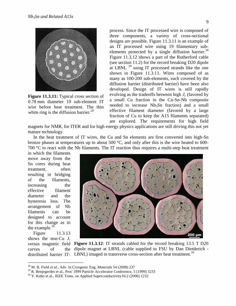
designs are possible. Figure 11.3.11 is an example of
an IT processed wire using 19 filamentary sub-
elements protected by a single diffusion barrier.28
Figure 11.3.12 shows a part of the Rutherford cable
(see section 11.2) for the record breaking D20 dipole
at LBNL 29
using IT processed strands like the one
shown in Figure 11.3.11. Wires composed of as
many as 100-200 sub-elements, each covered by the
diffusion barrier (distributed barrier) have been also
developed. Design of IT wires is still rapidly
evolving as the tradeoffs between high Jc (favored by
a small Cu fraction in the Cu-Sn-Nb composite
needed to increase Nb3Sn fraction) and a small
effective filament diameter (favored by a large
fraction of Cu to keep the A15 filaments separated)
are explored. The requirements for high field
magnets for NMR, for ITER and for high energy physics applications are still driving this not yet
mature technology.
In the heat treatment of IT wires, the Cu and Sn elements are first converted into high-Sn
bronze phases at temperatures up to about 500 °C, and only after this is the wire heated to 600-
700 °C to react with the Nb filaments. The IT reaction thus requires a multi-step heat treatment
in which the filaments
move away from the
Sn cores during heat
treatment, often
resulting in bridging
of the filaments,
increasing the
effective filament
diameter and the
hysteresis loss. The
arrangement of Nb
filaments can be
designed to account
for this change as in
the example.30
Figure 11.3.13
shows the non-Cu Jc
versus magnetic field
curves of the
distributed barrier IT-
28
M. B. Field et al., Adv. in Cryogenic Eng. Materials 54 (2008) 237 29
R. Benjegerdes et al., Proc 1999 Particle Accelerator Conference, 5 (1999) 3233 30
Y. Kubo et al., IEEE Trans. on Applied Superconductivity16:2 (2006) 1232
Figure 11.3.11: Typical cross section of
0.78 mm diameter 19 sub-element IT
wire before heat treatment. The thin
white ring is the diffusion barrier.28
Figure 11.3.12: IT strands cabled for the record breaking 13.5 T D20
dipole magnet at LBNL (cable supplied to FSU by Dan Dietderich -
LBNL) imaged in transverse cross-section after heat treatment.29

Nb3Sn and Related A15s
10
processed wire28
in which
~3000 A/mm² is achieved at 12 T,
as part of the US DOE HEP
Conductor Development Program,
nearly 3 times larger than that in
bronze-processed wires. However,
increasing the separation of Nb
filaments by enhancing the Cu:Sn
ratio to avoid filament bridging
reduces the Jc to the level of
bronze-processed wires. High-field
accelerator magnets are being
developed using IT-processed
Nb3Sn wires due to their large non-
Cu Jc. IT-processed Nb3Sn wire is
used also for fusion magnets, e.g.
ITER and KSTAR (Korea
Superconducting Tokamak
Advanced Research) facilities.
Comparing the bronze and IT
process, a clear advantage for the IT process is in the wire fabrication, since the bronze process
requires frequent intermediate anneals to soften the work-hardened bronze. However, it is not
possible to extrude composites containing Sn cores because of the danger of melting the Sn, so
temporary cores must be used which can be replaced by Sn at a later stage. The heat treatment
profile is also simpler for bronze wires. The Jc is larger in IT-processed wires, while AC loss is
smaller in bronze-processed wires. The n-value and the irreversible strain tend to be better in
bronze-processed wires. Thus there are advantages and disadvantages to both processes. Figure
11.3.14 illustrates the Nb3Sn layer Jc, reflecting the intrinsic quality of the Nb3Sn, versus
magnetic increase in Sn supply available in bronze processed wires31
. Furthermore the strain
effect in Nb3Sn wires which is practically an important topic has been extensively studied.34
11.3.5 Conclusions and Future Outlook
We have described a remarkable development of the A15 compound Nb3Sn from its “acci-
dental” discovery as a high-field superconductor 50 years ago in 1961 through rapid implementa-
tion as a tape conductor made either by CVD or by diffusion-processed Nb3Sn tapes and then to
its replacement by multifilamentary conductors, starting in the early 1970s. The discovery that
Cu could allow synthesis of V3Ga and Nb3Sn at much lower temperatures than was possible for
binary mixtures enabled this move to a multifilamentary technology. Additions such as Ti, which
enhanced Bc2(4.2 K) of Nb3Sn from ~21 T to ~26 T further enhanced the high-field capability of
Nb3Sn wires. Industrial fabrication of Nb3Sn wires was well established in the 1970’s on so that
31
P. J. Lee, A. A. Squitieri and D. C. Larbalestier, IEEE Trans. on Applied Superconductivity 10:1 (2000) 979 32
J. A. Parrell et al., Adv. in Cryogenic Eng. Materials 48 (2002) 968 33
A. Godeke et al., Cryogenics 48:7 (2008) 308. 34
J.W. Ekin, Adv. Cryogenic Engineering: Materials 30 (1984), 823 35
E. Gregory et al., Adv. Cryogenic Engineering: Materials 54 (2008) 252
Figure 11.3.13: Non-Cu Jc of distributed barrier IT wires
as a function of magnetic field. The Jc-B curves are nearly
identical for strands containing either 61 or 127 subele-
ment rods.28

Nb3Sn and Related A15s
11
it was not disrupted by the discovery of high-Tc cuprates in 1987. In the 1990’s and the 2000’s
marked improvements in the performance of Nb3Sn wire continued to be achieved using the
usual techniques of gaining a better understanding of manufacturing improvement and better
understanding of how to best package the mixture of Sn, Cu, Nb and Ti or Ta needed to produce
the superconducting A15 phase.
Because Nb-Ti cannot provide fields greater than 10-12 T, there is a clear market for high
field superconducting coils in the range up to now ~23 T that Nb3Sn can address. In fact
alternative processes to high performance conductors are still being explored. Besides the bronze
and IT processes, the PIT process, using powders of Sn-rich compounds such as NbSn2 or
Nb6Sn5,33
and the Nb tube process,35
yield Nb3Sn wires with excellent Jc performance and a
well-defined and small filament diameter. Such innovations show clearly that Nb3Sn has not yet
lost its place as the high-field superconductor, a rather remarkable state for the “original” high-
field superconductor 50 years on. Fresh water may still come out from an old spring in the
future.
Further Reading
1. In 1986 the Applied Superconductivity Conference celebrated the 75th Anniversary of the
discovery of superconductivity with a symposium on the history of superconductivity. The
symposium is published in full in IEEE Trans. Magn., 23, pp. 354-415, 1986
2. In 2008 a special edition of the journal Cryogenics brought together articles on the current
Figure 11.3.14: The layer Jc of the Nb3Sn in a variety of Nb3Sn strands. The higher Sn contents
available in PIT and high-Jc type IT strands can double the intrinsic Jc of the Nb3Sn.31
RRP®:
Restacked Rod Process (IT)28
, MJR: Modified Jelly Roll (IT)32
, PIT: Powder in Tube33
.

Nb3Sn and Related A15s
12
state of the art of low temperature superconductor science and technology: Cryogenics 48
(2008)
3. A history of technical superconductors in Russia, including Nb3Sn, is covered in: A.K. Shikov
et al., "The History of Technical Superconductors Development in Russia," IEEE Transactions
on Applied Superconductivity 17, no. 2 (2007): 2550-2555.