acknowledgments - maglabfs.magnet.fsu.edu/~lee/asc/pdf_papers/theses/mbf96phd.pdf ·...
TRANSCRIPT

xiii
Acknowledgments
This thesis was not done in a vacuum (no pun intended). There are too many
people to thank individually, but let’s give it a try. First, there is my advisor Professor
David Larbalestier, who guided and focused the thinking behind the experiments and
secured funding for both myself and the necessary equipment. Then there is Dr. Xueyu
Cai, who taught me basically everything I know about electromagnetic testing of
superconductors. Long discussions on the art of Chinese cooking were invaluable as well.
Also there are the magneto-optic imaging scientists (Dr. Anatoly Polyanskii and Alex
Pashitski), who provided the lovely magneto-optic images shown in Chapter 4. Fellow
graduate students, spanning the generations from Henry Muller on down to Michael Naus,
played a key role as well, from helping with equipment problems, to maintenance of the
group computers, to creating the general feeling of camaraderie of the “6th floor” which
made my rather long stay an enjoyable one. Fellow graduated student Harry Edelman
deserves special notice for developing the pulsed current measuring system, which was
quite useful for measuring many of the samples in this thesis. Also of critical importance
was the staff assistance of Bill Starch and Alex Squitieri, who made rigs and maintained
magnet systems that were used in my work.
Other research groups influenced my work as well. Professor Susan Babcock and
her students helped in my understanding of the structure and properties of grain
boundaries. Collaborators at the Texas Center for Superconductivity, Apurva Parikh and

xiii
Professor Kamel Salama, provided samples used for the second set of melt-textured grain
boundary experiments. Dr. Sungho Jin of AT&T and Dr. Tom Luhman of Boeing also
provided samples that were studied in this thesis. The professors and students of the UW
“MRG” helped as well with important feedback, and thanks should also be accorded the
National Science Foundation, for providing the Materials Research Group grant which
provided the financial backing which made this all possible.
Last but not least, thanks to my parents and family, for keeping the fires burning on
the homefront. I can now answer the question my family has been asking me for years:
“But when are you going to be finished?”
Now!

xiii
Table of Contents
Chapter 1 : The Challenge: Bulk Conductor Applications for
YBa2Cu3O6+X _________________________________________________ 1
Chapter 2 : YBa2Cu3O6+x: Processing, Electromagnetic Behavior and Grain
Boundaries __________________________________________________ 12
The YBa2Cu3O6+x Phase Diagram ______________________________________________ 14
Melt-Texturing of YBa 2Cu3O6+x________________________________________________ 23
Determining the Coupling Characteristics of the Grain Boundary ___________________ 31
Essential Structural Features of Grain Boundaries________________________________ 36
Chapter 3 : Initial Melt-Textured YBa2Cu3O6+x Bicrystal Experiments __ 43
Sample Fabrication__________________________________________________________ 43
Bicrystal Isolation ___________________________________________________________ 48
Misorientation Determination - X-Ray Pole Figures _______________________________ 52
Electromagnetic Testing______________________________________________________ 61
Results ____________________________________________________________________ 65
Discussion _________________________________________________________________ 72

xiii
Chapter 4 : Experiments with Melt-Out, Melt-Texture (MOMT) YBCO _ 75
Sample Fabrication and Isolation ______________________________________________ 78
New Electromagnetic Techniques - Pulsed Current and High Voltage Sensitivity ______ 80
Magneto-Optical Imaging_____________________________________________________ 86
Electromagnetic Results ______________________________________________________ 87
Magneto-Optical Imaging Experiments _________________________________________ 98
Results - Role of the Macroscopic Grain Boundary Plane _________________________ 105
Discussion ________________________________________________________________ 110
Chapter 5 : Summary and Conclusions __________________________ 123
Appendix A: The Mixed Misorientation Description ________________ 129
The Mixed Misorientation Description - General Grain Boundary Geometry _________ 129
The Mixed Misorientation Description - Example________________________________ 136
Appendix B: Laser Cutting of YBa2Cu3O6+x_______________________ 141
References _____________________________Error! Bookmark not defined.

xiii
Table of Figures
Figure 1-1) The irreversibility fields, a measure of the vortex pinning strength, as a functionof temperature fraction of Tc for YBCO, Bi-2212, Bi-2223, and La-214. Plot fromSuenaga et al. [2]............................................................................................................2
Figure 1-2) Drawings illustrating the thin film YBCO grain boundary geometry of Dimos etal.[14]: a) [001] tilt b) [100] tilt c) [100] twist. ..............................................................4
Figure 1-3) The plot of the ratio of the intergranular to intragranular critical currentdensities for YBCO thin films on SrTiO3 with three different primary misorientationgeometries - (001) tilt, - (100) tilt, - (100) twist, at 5K and no appliedmagnetic field, from Dimos et al.[14].............................................................................5
Figure 1-4) Plot of transport Jc(B) for flux-grown bulk YBCO bicrystals with H//c, 77K foran intragranular region (), and the 3°[001] tilt (), 15°[001] tilt (), 90°[010] parttilt/part twist () bicrystals. Adapted from Babcock et al.[4]......................................7
Figure 2-1) The typical microstructure of polycrystalline sintered YBCO, view underpolarized light, from Verhoeven[]. The brightness contrast between the grains is dueto the crystal misorientation, and the striations visible within the grains are twinboundaries (major tick=10µm, minor tick=1µm).........................................................13
Figure 2-2) Drawing of the perovskite crystal structure, where A and B are metallic cationsand X is a non-metallic anion. The YBCO unit cell is composed of three of theseperovskite unit cells stacked: the center cell has Y as the A cation, and the top andbottom cells have Ba as the A cation. In both cases, Cu is the B cation and O is the Xanion, as shown in Figure 2-4.......................................................................................15
Figure 2-3) Schematic diagram of twin trace pattern. A 90° cross pattern generallyindicates viewing plane normal to c axis, parallel twins indicate viewing planes parallelto c-axis. .......................................................................................................................16
Figure 2-4) Drawing of the YBCO unit cell, orthorhombic and fully oxygenated to O7. TheCuO2 planes are kinked. Vacancies for O<7 occur mainly at the O1 and O5 locations,with some on O4 as well[]. Drawing from ref. [48]. ...................................................18
Figure 2-5) Graph of the Tc of YBa2Cu3O6+x as a function of oxygen stoichiometry (x).Solid points are calculation, open points are experimental data[,]. From Poulsen etal.[54]. ..........................................................................................................................19
Figure 2-6) The YO1.5-BaO-CuO pseudoternary phase diagram at 950°C in air. The tielines indicate that the 123 phase is stable with the 211, CuO, and BaCuO2 phases at950°C. These are the common impurity phases detected when trying to form 123.Phase diagram from Beyers and Ahn[]. .......................................................................20

xiii
Figure 2-7) Space model of the YBCO phase diagram with the primary crystallization fieldfor 123 shaded. Note that this field is quite small and is Ba- and Cu- rich with respectto the 123 composition. Phase diagram from Maeda et al.[65]...................................22
Figure 2-8) Vertical binary slice of YBCO pseudoternary in air (Figure 2-6). Phasediagram from Murakami et al.[] ...................................................................................23
Figure 2-9) Schematic diagram of 123 grain nucleation and growth. Note that the growthof 123 shell around the 211 hinders completion of the peritectic reaction. Diffusionand growth is much faster in the ab plane than in the c-direction................................25
Figure 2-10) Typical microstructure of a melt-textured YBCO grain, viewed underpolarized light. The primary twinned phase is 123. Because the twin traces are~90°from each other, this indicates that the c-axis is approximately normal to the samplesurface. The darker, elliptical second phase, with around 30% of the volume, is211…............................................................................................................................25
Figure 2-11) Cracks (or gaps), originally thought to be platelet twist boundaries, areindicated by the arrows. The twin trace pattern (the smaller angle between the twinsis less than 90° but greater than 0°) indicates the c-axis of the sample is inclined fromthe sample surface (see Figure 2-3) and hence the cracks in the ab-plane are visible.26
Figure 2-12) A drawing illustrating that the lines in the ab direction of melt-textured 123are not grain boundaries but gaps as a result of the growth process filled with secondphase, such as CuO,[69] or cracks due to the tetragonal to orthorhombictransition[70,71]. They do not extended across the width of the sample, and socurrent can flow along the c-axis of the specimen without crossing a grain boundary.Drawing adapted from Alexander et al.[69].................................................................26
Figure 2-13) A simple drawing of the melt-out, melt-texturing process before texturingbegins. The sintered 123 bar is melt-textured on a 211 bar. During melt-texturingsome 30-40% of the liquid, including possible impurities, is wicked into the porous,low density 211 block. Drawing adapted from Willen and Salama[95]......................30
Figure 2-14) Typical V-I traces for a strongly-coupled 90° grain boundary. The key featureis that low applied magnetic fields do not diminish the Ic. Plot taken from Babcock etal.[4] .............................................................................................................................32
Figure 2-15) Plot of the smooth flux-flow V-I characteristic of a strongly-coupled melt-textured 5° grain boundary at 0.4T and 77K................................................................33
Figure 2-16) Plot of V-I curves of UW melt-textured high angle (55°[ 2 3 1 ]) bicrystalMB4C1. Low magnetic fields greatly decrease the supercurrent from the zero fieldvalue, and the resistive transition is ohmic...................................................................34

xiii
Figure 2-17) a) Two cubic crystals are misoriented by θ about [001]. b) When the crystalsare joined, the mismatch can be accommodated by elastic strain and edge dislocations(⊥) spaced b/θ, where b is the burgers vector. Drawing from Read[105]. .................37
Figure 2-18) Plot of dislocation spacing in a [001] tilt grain boundary as a function ofmisorientation angle for two different burgers vectors observed by I-Fei Tsu[104].Plot from Tsu[104]. ......................................................................................................38
Figure 2-19) The graphical definition of Σ. The left image shows the atomic positions thatcomprise the two crystal lattices of the grains of a bicrystal. The right image showsthe overlap the atoms from one grain of a bicrystal onto the other grain, and a patternof coincident points that may appear. The number of atoms that comprise eachcoincident cell is the Σ value, the lower the number indicating the higher thecoincidence. Figure from Merkle[]..............................................................................41
Figure 2-20) Schematic plot of grain boundary energy vs. misorientation angle. At certainhigher angle misorientations there exists special low energy grain boundaries. Plotadapted from Chan[]. ...................................................................................................42
Figure 3-1) The melt-texture process: plot of temperature vs. time, based on the proceduredeveloped by Salama et al.[5]. The quick initial heating creates a melt of 211+liquid.The key grain growth step is the 50 hrs. slow cool through the peritectic. Oxygenationoccurs below 600°C. ....................................................................................................45
Figure 3-2) Polarized light micrograph of the amorphous non-superconducting and BaCuO2
and CuO phases resulting from an incomplete peritectic reaction duringresolidification from the melt (light gray in the image). The majority, matrix-phase isYBCO...........................................................................................................................47
Figure 3-3) The circled regions of this polarized light micrograph highlight large,amorphous, non-superconducting phases at the grain boundary. Contamination at thissize scale will clearly result in an insulating grain boundary........................................47
Figure 3-4) Polycrystalline melt textured sample from AT&T[44], thinned and polished,and viewed under polarized light. The different regions of contrast represent grains ofdifferent orientation. The very small dots are 211, and the larger circles are voids. ..49
Figure 3-5) Polarized light micrograph of the top and bottom surfaces of sample SJ3151B3,which has been thinned to 50µm. The boundary goes completely through thesample….......................................................................................................................50
Figure 3-6) Polarized light micrograph of a melt-textured sample from AT&T[44] that waspolished in bar form on four sides. Placing these images together, one can choose adirection to polish from so as to isolate a desired bicrystal..........................................51

xiii
Figure 3-7) A melt-textured high angle grain boundary (MT4C2.2 - 57°[17 11 2]) viewedunder polarized light. Twins do not intersect at 90°, indicating that both grains haveinclined c-axes. The grain boundary plane is macroscopically wavy..........................53
Figure 3-8) Schematic diagram of the x-ray pole figure apparatus showing how the keyangles θ, χ, and φ are related to the x-ray source, detector, and sample. ....................55
Figure 3-9) Schematic diagram to show how rotations of φ produce Bragg reflections whichlie on a conical surface. Maximum χ in reflection mode is ~80° and φ rotates the full360° for each χ.............................................................................................................56
Figure 3-10) Automatic “raw” pole figure data for sample MB4C1. The location and widthof the labeled poles are used to approximate the pole centroids. They are then locatedmanually by scanning in 1° increments. .......................................................................58
Figure 3-11) A 2θ scan for the (006) pole of a sample (MB4C1) located at χ=62° andφ=277° shows a peak intensity of ~2100 counts per second at 2θ=46.6°. ..................59
Figure 3-12) Map showing the centroid of a c-axis via the peak counts per second values(X=not measured) at an experimentally determined 2θ=47° for sample KS4B2. Thecentroid is at χ=78°, φ=98°, width ~±1°. .....................................................................59
Figure 3-13) Polarized light micrograph of a UW MT sample was not measured because ofthe crack which extended across both grains...............................................................62
Figure 3-14) Schematic diagram of the AC Tc experimental system. The sample is cooledin a He gas filled rig, down to either 77K or 4K. The temperature sensor in the rig isread by the temperature controller and relayed to the computer chart recorder. Thevoltage signal (at the same frequency and phase as a generated current of a knownlevel) is read by the lock-in amplifier and sent to the computer chart recorder. Data isdisplayed as voltage versus temperature, but this is easily converted to resistanceversus temperature as the current level is preset..........................................................63
Figure 3-15) Schematic diagram of the DC V-I measurement setup. A ramp controllermanually triggered a BOP to provide the current for the sample while a DC voltmeterread the response..........................................................................................................64
Figure 3-16) Plot of Jc(B,θ,77K) characteristics for melt-textured bicrystals at lowmagnetic fields. Zero field Jc decreases and the field dependence of Jc increases withincreasing misorientation..............................................................................................66
Figure 3-17) High field residual critical currents measured in five melt-textured high angleboundaries at 4K. Higher angle boundaries tend to have lower Jc values...................67
Figure 3-18) A typical AC Resistive Tc trace across a melt-textured boundary (sampleMB4C3b). The Tc onset is at ~91K, with zero resistance occurring at T=90.2K........68

xiii
Figure 3-19) For sample SJ3151B3 the Tc onset is at 91K, but a resistive tail, believed to bedue to dissipation at the grain boundary, is visible down to 88K for a measuringcurrent of 10mA (J~100A/cm2)....................................................................................69
Figure 3-20) Two bicrystals exhibited a sharp low field depression of Jc but then exhibited amuch slower fall off in strong fields at 77K (B is not ||c for either sample).................71
Figure 4-1) Illustration of seeded melt-textured bicrystal growth. Single crystals of alignedY-123 grow from the Sm-123 seeds and create a grain boundary dictated by themisorientation of the Sm-123 seeds..............................................................................79
Figure 4-2) Polarized light micrograph of the wiring of a typical laser-isolated bicrystal(KS4B1a). The sample is only 85µm thick and 370µm wide, but ~3.5mm long,allowing space for four voltage taps. Note that the current leads are large anddesigned to feed current into the whole cross-section of the sample...........................80
Figure 4-3) Gold pads, ~50-100µm in diameter were sputtered on the surface through acopper grid in an attempt to get lower contact resistivity (Sample KS4B1c)...............81
Figure 4-4) Schematic diagram of pulsed current experimental circuit. The computertriggers the function generator which defines the shape of the pulse. The functiongenerator than creates the current pulse through the bi-operational power supply. ....82
Figure 4-5) Plots of the current pulse and voltage response vs. time. The voltage responseto the 1ms pulses has both a leading and trailing inductive spike. The choice ofvoltage measuring window results in a tradeoff between voltage noise and voltagebaseline. Plots adapted from Edelman[136]................................................................83
Figure 4-6) Schematic diagram of the high sensitivity V-I experimental setup. The keyfeature is the Keithley voltmeter/preamp combination which can achieve nVsensitivity under optimal conditions.............................................................................84
Figure 4-7) Plot of intergranular Jc(B, 77K), determined by pulsed V-I measurements forMOMT samples of general misorientation of 5° through 38°. Inset shows details ofthe low field behavior...................................................................................................88
Figure 4-8) Plot of the intergranular critical current density in magnetic field, Jc(g.b.)(B),expressed as a ratio of the zero field value at 77K for the samples of generalmisorientation (5° through 38°)....................................................................................89
Figure 4-9) A comparison of the intergranular Jc of the 38°[3 1 1] Boeing bicrystal and the38°e[15 -14 1] MOMT bicrystal...................................................................................91
Figure 4-10) Plot of the intergranular log V-J characteristics for sample 11°b at77K(H~||c)....................................................................................................................93
Figure 4-11) Plot of intragranular (grain B) log V-J characteristics for sample 11°b at77K(H~||c)....................................................................................................................94

xiii
Figure 4-12) Plot of intergranular log V-J characteristics for sample 38°e at 77K. .............95
Figure 4-13) Plot of intragranular (grain B) log V-J characteristics for sample 38°e at77K…...........................................................................................................................96
Figure 4-14) a) Polarized light micrograph of the 5° bicrystal b) reflected light MO image at15K in 40mT. The c-axis of each grain is ~9° from surface plane. Flux penetratespreferentially along cracks between platelets and at large 211 particles but not at theGB ................................................................................................................................98
Figure 4-15) Polarized light micrograph of the 11°c bicrystal b) reflected light MO image at15K in zero field after field cooling in 40mT. Regions A, B, and C pin flux better thanadjacent segments of the boundary ............................................................................100
Figure 4-16) a) Polarized light micrograph of the GB in sample 14°b. b) Magneto-opticimage of the same region. The image was taken after being field cooled to 8K in40mT..........................................................................................................................102
Figure 4-17) Smoothed data from pulsed V-I traces on 14°b as a function of magnetic field.There is a sharp decline in the Ic in low magnetic fields, but the inset highlights a farless field-dependent Ic. ...............................................................................................103
Figure 4-18) Polarized light micrographs of sample 7°a and 7°b. The grain boundary in 7°ais curved while the GB in 7°b has two ~90° kinks. Applied current direction is alongthe long sample dimension as indicated. ....................................................................105
Figure 4-19) A plot of the ratio of the intergranular Jc(B) vs. the lower intragranular Jc(B)for samples 7°a and 7°b at 77K..................................................................................106
Figure 4-20) Polarized light micrographs of samples 11°a, b, and c. The boundary planes in11°a and 11°b have similar inclinations to the samples’ long axis, while 11°c is nearlynormal to the long axis. Applied current direction is along the long sample dimensionas indicated.................................................................................................................107
Figure 4-21) Plot of the Jc(B,77K) characteristic for samples 11°a, b, c. ..........................108
Figure 4-22) Polarized light micrographs of samples 38°a, c, d showing the different grainboundary plane inclinations. Current direction is along the long sampledimension…… ...........................................................................................................109
Figure 4-23) Schematic drawings of three models for explaining the GB Jc in thin film [001]tilt YBCO as a function of GB structure: a) The dislocation core model [14,15], beforeand after core overlap, b) The Dayem bridge model[141], and c) Two channelmodel[42,146]. ...........................................................................................................114
Figure 4-24) Schematic representations of the possible microstructure viewed in the GBplane (GB normal is out of the paper) of a) the prison bar model of a simple [001] tiltboundary. The black regions are the dislocation cores, the gray are the areas near the

xiii
cores that are degraded due to strain, while the white areas represent undisturbedlattice. Note the large 2-D rectangular regions of this undisturbed lattice. b) Generalmisorientation GB, composed of a grid of 4 sets of dislocations, results in ageometrical network of essentially point, rather than line contacts (adapted fromMiranova et al.[150]). ................................................................................................116
Figure 4-25) Plot of the Jc(g.b.)(B=0, 77K) values for flux-grown ([20,152]), melt-textured(UW/AT&T MT - [22], MOMT - [33], UW MT - [22], Boeing seeded -
[151], Argonne seeded - [93]) and thin film (Ivanov et al. - z[153], Heinig et al.- [146]) bicrystals, as a function of general misorientation angle. .........................117
Figure 4-26) Plot of the ratio of the intergranular to intragranular critical currents (0T, 77K)for melt-out samples (zz, ), in comparison to other general misorientation, UW melt-textured samples previously measured at 77K()[22],()[151], Argonne seededmelt-textured bicrystals ()[93], UW/NIST [001] tilt bulk flux-grown bicrystals at77K( )[20,152], thin film samples of mixed misorientation at 5K() by Dimos etal.[14], [001] tilt thin film samples at 77K() by Heinig et al.[146], and [001] tilt thinfilm samples at 77K(∆) by Ivanov et al.[153]. Symbols with white crosses indicatethat the intragranular Jc was estimated, while all other samples had measuredintragranular Jc values. Second order regression fits to all the bulk scale and thin filmdata illustrate that bulk scale grain boundaries tend to have a weaker decline of Jc(g.b.)
with increasing misorientation angle than the thin film boundaries. ..........................119
Figure 4-27) Plots of the ratios of the intergranular to intragranular critical currents as afunction of applied magnetic field at 77K: a) Jc(B) for the inter and intragranularregions of sample 7°a with B~⊥c, b) The ratio of intergranular Ic to intragranular Icwith B~⊥c, c) Jc(B) for the inter and intragranular regions of sample 7°a with B~||c, d)The ratio of intergranular Ic to intragranular Ic with B~||c. ........................................122
Figure 5-1) Plot of the estimated Jc(g.b.)/Jc(grain)(77K) ratios at zero field for IBAD tapes(zz)[155] vs. thin film (TF) bicrystals ()[146,153]. The intragranular Jc value forIBAD tapes is estimated at 2X10⁶A/cm2, a standard YBCO TF value[152]. The IBADratios are consistently higher than the TF ratios above 10°. ......................................126
Figure 5-2) Plot of the estimated Jc(g.b.)/Jc(grain)(77K) ratios at zero field for IBAD tapes (zz)vs. bulk bicrystals (, flux grown[20,152] and melt-textured[22,151,93]). The IBADratios lie among the bulk bicrystal ratios....................................................................127
Figure A-1) a) Schematic drawing of a general misorientation grain boundary with a flatgrain boundary plane. b) The misorientation between crystal abc and a’b’c’ in a) canbe described by a rotation angle θ about a rotation axis u that sets both crystalcoincident. The grain boundary normal n is independent of θ and u. .......................130

xiii
Figure A-2) a) Drawing of a tilt grain boundary: the rotation axis is perpendicular to thegrain boundary plane normal (u⊥n). b) Drawing of a twist grain boundary: therotation axis is parallel to the grain boundary plane normal (u||n). ............................133
Figure A-3) Graphical definition of the Euler angles (Θ, Φ, and Ψ). The misorientationbetween two crystals of axes xyz and x’y’z’ can be described by a rotation about z,followed by a rotation about x’’, and then a rotation of about z’. Figure adapted fromRandle[118]................................................................................................................135
Figure A-4) Pole figure data plotted on a stereographic projection, with each point acentroid of the labeled pole. The orthorhombic structure of YBCO constrains whichpole belongs to which crystal. ....................................................................................137
Figure A-5) A Wulff net, used to measure angles from a stereographic projection. Thelongitudinal lines are known as the “great circles.” ...................................................138
Figure A-6) The poles marked on Figure A-4 are rotated so that the c’ and c poles lie onthe same great circle. Then the misorientation angle between c and c’ can bedetermined by noted the angular distance on the great circle (θcc’=41°). ..................140
Figure B-1) Schematic drawing of the thermoevaporation process from ref.[159]. Laserbeam first melts the material and then heats the liquid until the vapor phase is formedand ejected from the cut.............................................................................................142
Figure B-2) Plot of ablation depth per laser shot as a function of laser wavelength, fromref.[161]......................................................................................................................144
Figure B-3) Drawing of the Florod Nd:YAG laser, from the Florod LMS Manual[]. Thisassembly is mounted with the tilt plate attached to the top port of a long workingdistance Mitutoyo microscope. ..................................................................................145
Figure B-4) An unpolarized light micrograph of a melt texture sample cut with a Nd-YAGlaser a) before and b) after cleaning with methanol. The discoloration surround thecut in the first image is due to re-deposit material from the cut, and is not sampledamage. ......................................................................................................................146

xiii
Index of Tables
Table 3-1: Summary of misorientation, Tc, grain boundary Jc electromagnetic coupling, andgrain boundary resistivity (ρnd) for UW and AT&T manufactured MT bicrystals. .....65
Table 4-1: Misorientation angle, common axis and illustrative electromagnetic data forvarious bicrystals..........................................................................................................87
Table 4-2 Comparison of irreversibility fields of the grain boundary and the grains forvarious MOMT bicrystals at 77K.................................................................................97
Table B-1: Bouguer’s constants for different laser wavelengths[160]...............................144

1
Chapter 1 : The Challenge: Bulk Conductor Applications for
YBa2Cu3O6+X
The main obstacle on the road to practical bulk conductor applications of the
superconductor YBa2Cu3O6+x ("YBCO") is the inability to pass large supercurrents (~105-
106A/cm2) through this material’s grain boundaries in the presence of strong magnetic
fields. The material, a black, brittle, complex copper-oxide discovered in 1987[1], has a
critical temperature above the 77K boiling point of liquid nitrogen (Tc=92K), as well as an
extremely high upper critical field (Hc2(77K)>>10T for fields in the ab plane). It also has
strong vortex pinning even at 77K in significant magnetic fields (>1T), as shown by its
superior irreversibility field (the magnetic field above which Jc becomes zero) behavior in
comparison to other ceramic high temperature superconducting oxides: Bi2Sr2CaCu2O8 (Bi-
2212), Bi2Sr2Ca2Cu3O10 (Bi-2223) and La1.85Sr0.15CuO4 (Figure 1-1)[2], as well as the Tl-
and Hg- based superconducting ceramic oxides. Although the brittle nature of YBCO
presents a serious challenge to manufacture of a flexible conductor form, various
fabrication methods, such as the powder-in-tube process[3], overcome this obstacle.
Intragranular current densities in the bulk forms of YBCO are generally good; they range
from ~103A/cm2 in flux-grown single crystals[4], to ~104-105A/cm2 for melt-textured
material[5,6], and up to 106A/cm2 in thin film single crystals[7].

2
Figure 1-1) The irreversibility fields, a measure of the vortex pinning strength, as afunction of temperature fraction of Tc for YBCO, Bi-2212, Bi-2223, and La-214. Plotfrom Suenaga et al. [2].
However, a major problem remains for YBCO. This is its inability to carry usable
critical current densities (i.e., > 105A/cm2) across misaligned grains. Deutscher and
Müller[8] predicted that since the coherence length (ξ0(ab)~16Å, ξ0(c)~2Å)[9] is of the same
order as the grain boundary thickness, the atomic scale grain boundary disorder would
severely depress the superconducting order parameter at the grain boundary. Indeed, bulk
polycrystalline material has poor transport Jc despite good intragranular magnetization
Jc[10]. However, granularity has not been as severe a problem in the Bi-compound family
despite similarly small coherence lengths (e.g., Bi-2212: ξ0(ab)~30Å, ξ0(c)~4Å, 77K)[11].
This improved behavior is believed to be simply a result of the micaceous properties of the

3
double Bi-O layers in BSCCO compounds, which allows them to be textured to a high
degree (i.e., the grains are better aligned) by a series of rolling and heat treatment
steps[12]. It is an open question whether there are intrinsic differences in the nature of the
grain boundaries in YBCO and BSCCO.
The first experiments to show explicitly the influence of the grain boundary on
YBCO current transport, specifically the effect of the misorientation of two crystals across
a grain boundary, were those of Dimos et al.[13,14]. By using thin films grown on SrTiO3
bicrystal substrates of controlled misorientation angle, they demonstrated a strong
relationship between the Jc and misorientation angle of either [100] twist, [001] and [100]
tilt bicrystals (Figure 1-2). They concluded that grains misoriented by more that ~5°-10°
are always weakly-coupled. This was inferred from measurements of the ratio of the zero
field intergranular to the intragranular critical current densities (Jc(g.b.)(0T,5K)/Jc(grain)), which
showed ratios of the order 0.01-0.05 for high angle boundaries, as compared to a 0.5-1
ratio for low angle grain boundaries (Figure 1-3). They further proposed that all YBCO
grains misoriented by more than ~5°-10° are intrinsically weak-linked, because the grain
boundary acquires a suppressed order parameter produced by the grain boundary
dislocation core overlap. While the physical size of these dislocations does not suggest an
effective overlap until ~20°, it was also proposed that the strain fields associated with the
dislocations can increase their effective diameter so as to cause overlap at ~10°[15],
provided that the boundary does not relax to a lower strain configuration. Other studies on

4
thin film Bi and Tl-2212 bicrystals have shown similar Jc(g.b.)(0T)/Jc(grain), results[16,17],
resulting in strongly suppressed Jc(0T, 77K(Tl), 4K(Bi)) above ~10°[001] tilt.
Figure 1-2) Drawings illustrating the thin film YBCO grain boundary geometry ofDimos et al.[14]: a) [001] tilt b) [100] tilt c) [100] twist.

5
Figure 1-3) The plot of the ratio of the intergranular to intragranular critical currentdensities for YBCO thin films on SrTiO3 with three different primary misorien tationgeometries - (001) tilt, - (100) tilt, - (100) twist, at 5K and no appliedmagnetic field, from Dimos et al.[14].

6
The generality of these conclusions, especially the small value of the crossover
misorientation angle from strong to weak coupling, was put in some doubt by subsequent
work done at the University of Wisconsin on bulk-scale, flux-grown YBCO bicrystals.
Babcock et al.[4] showed two high angle grain boundaries (14°[001] tilt and 90°[010] tilt
and twist) to be strongly-coupled (Figure 1-4). Eom et al. later showed that 90°[010] tilt
thin films were also strongly-coupled[18,19]. This strong-coupling is indicated by an
intergranular Jc(B) that is similar to the intragranular Jc(B), in that it is insensitive to low
magnetic fields and has a similar decay in high applied fields. Larbalestier et al.[20] later
showed evidence for weakly-coupled, or Josephson Junction (JJ), behavior and strongly-
coupled, or flux-pinning (FP), behavior for different bicrystals of the same misorientation
(e.g., 14°[001] tilt). Recently, the variability of the Jc(g.b.)(0T,77K)/Jc(grain) was shown by
Heinig et al.[21] for 7° YBCO thin films made with the same growth parameters and the
same substrates. These results demonstrate that the explanation for grain boundary
properties cannot be as simple as Dimos et al.[14] proposed. Thus the grain boundary
properties are not only a function uniquely defined by their misorientation, and ~5°-10° of
misorientation is not necessarily the strong-coupling limit.

7
Applied Field (T)
0 2 4 6 8
Crit
ical
Cur
ren
t Den
sity
(A
/cm
2 )
0
1000
2000
3000
77K
Figure 1-4) Plot of transport Jc(B) for flux-grown bulk YBCO b icrystals with H//c,77K for an intragranular region (), and the 3°°[001] tilt (), 15°°[001] tilt (),90°°[010] part tilt/part twist ( ) bicrystals. Adapted from Babcock et al.[4].

8
Further investigation of certain bulk samples revealed that, a nearly field-
independent, though small, critical current component remained[20,22] for magnetic field-
sensitive, Josephson-like boundaries even at high fields. This residual critical current is not
well explained as a property of a typical Josephson Junction, as few reports on low Tc JJ
addressed high field properties directly. A report by Yanson[23] did show experimentally
that structural inhomogeneities in a Sn-Sn tunnel junction resulted in a plateau in the Jc(B)
character, in direct contrast to the typical Fraunhofer-like Jc(B). More recently, Bulaevskii
et al.[24] extended this analysis to the high field case to develop a “brick wall” model of
current transport in Bi-oxides c-axis JJ boundaries, where the observed macroscopic
transport current in Bi tapes is the residual current of the c-axis JJ. Another feasible
explanation is that high angle grain boundaries have a small strongly-coupled path, in
parallel with a majority weakly-coupled connection.
The variety of behavior exhibited by grain boundaries of similar misorientations
shows that misorientation is not the only factor controlling boundary character, thus
focusing attention on other possible variables. One such factor that is not yet well
understood is the role of impurities and other composition variations at the grain boundary.
The atomic disorder of the grain boundary permits rapid diffusion of oxygen, as well as
permitting impurity contamination. Local oxygen deficiency has been shown to be
important, as grain boundary regions have been correlated with weak-coupling by electron
energy loss spectroscopy[25]. Impurity segregation effects are potentially important
because of the possibility of SrTiO3 substrate contamination in thin film bicrystals and the

9
potential for CuO-BaCuO2 contamination from the flux in flux-grown bicrystals. These
two systems have provided the source material for most of the experiments on grain
boundary behavior. Thus, it would be more desirable for probing the intrinsic grain
boundary disorder effects on the electromagnetic properties of bicrystals to obtain
boundaries that are produced in a less contaminant-rich environment.
How are these results relevant to bulk scale applications of YBCO? Bulk scale
applications of any high temperature superconductor almost certainly require that some
degree of misorientation from one grain to another be tolerated. In the past few years,
several methods of combating the granularity of YBCO by various texturing routes have
been demonstrated. The most dramatic has been the Ion Beam Assisted Deposition
(“IBAD”)[26] process. On a randomly oriented Ni-alloy (Hastelloy) tape, a biaxially
textured yttrium-stabilized zirconia (YSZ) film is sputtered with one ion beam (Ar+), while
a second, assisting ion beam (O+Ar) bombards the film to induce texture. A YBCO film of
up to ~1µm thickness is then deposited on the YSZ. Such tapes can have Jc(75K,
0T)~106A/cm2 with little evidence of weak links in magnetic fields[27]. It is important to
note that the YBCO in IBAD tapes is not fully aligned; rather full width at half maximum
(FWHM) of the (103) rocking curves of the YBCO range from 10.5°[27], to as high as 20°-
30°[26]. It should be noted that the creation of the aligned YSZ substrates is quite time
consuming.
Another promising report involves the use of textured metal substrates created by
rolling, called Rolling Assisted Biaxial Textured Substrates (“RABiTS”)[28]. It involves a

10
textured substrate, presently Ni, which has been cold rolled and recrystallized to a sharp
cube texture. This is followed by depositing a layer of the noble metal Pd and then CeO2
and/or YSZ as an appropriate aligned deposition template for the YBCO. The resultant
substrate has 95% of the grain boundaries with misorientations of 10° or less. A 0.75µm
thick film had a Jc(77K, 0T)=3 x 10⁵A/cm2. While the Jc is not quite as high as IBAD, it
should be technologically simpler to scale up.
The third promising report on texturing of YBCO is a thick film approach, called
Magnetic Field/Liquid Assisted Texture (“MFLAT”)[29]. It involves the high field (7T)
magnetic alignment of YBCO thick films during partial melting on silver. While the critical
current densities are more modest, Jc(77K, 3T)=2 x 10³A/cm2, they involve samples of
much larger grain size (dimensions of tens to several hundred µm) and total thickness
(1mm). Thus the Ic values are larger than samples made by the IBAD and RABiTS
techniques, with ~100A for MFLAT, in comparison to 50A for IBAD, at 77K and 1T[30].
The thick film Jc values of the MFLAT process are a significant improvement across grain
boundaries in sintered YBCO with similar grain dimensions, and the FWHM of the (103)
rocking curve is 9°[31].
These positive reports underscore the importance of studying and understanding the
electromagnetic properties of grain boundaries of general misorientation. These samples
have misorientations with significant tilt and twist components, yet the bicrystal
experiments in the past have focused on the geometrically simpler thin film (TF) and flux-
grown (FG) bicrystals. This was because the grain boundary misorientations can be clearly

11
defined, compared to existing grain boundary models, and the samples are suitable for high
resolution transmission electron microscopy (HRTEM). How well the simpler geometries
can be used to predict behavior in the more general misorientations is not well known. In
fact, there is evidence to suggest that the behavior in the general misorientation bicrystals
may be less sensitive to misorientation than TF bicrystals, despite their more complex
geometry[32,33]. Other researchers have investigated general misorientation boundaries in
the YBCO family[34,35,36,37,38,39,40,32,41], but the work presented here provides the
most thorough and complete combination of misorientation and electromagnetic analysis to
date on these types of grain boundaries.
The organization of the thesis is as follows: in Chapter 2 I will present background
information on sample processing, the electromagnetic definitions of coupling character,
and brief explanations of the grain boundary models used in describe superconducting
bicrystals. In Chapter 3 I will describe the experimental procedures and discuss the results
of the initial UW melt-textured YBCO experiments, during ~1990-1994[22]. In Chapter 4
I will describe the second round of melt-textured experiments, featuring “melt-out”
samples, analyzed from ~1994-1996[42,43,33]. I will then attempt to draw conclusions
from both sets of data, with a look towards the implications towards the future of YBCO
bulk applications. Appendices on crystallographic misorientation descriptions and laser
cutting of YBCO are included for reference.

12
Chapter 2 : YBa2Cu3O6+x: Processing, Electromagnetic Behavior and
Grain Boundaries
The initial goal of my thesis was to perform electromagnetic experiments on
sintered bulk YBCO similar to the thin film experiments by Dimos et al.[14]. The
motivation was that the magnetic field dependence of Jc for bicrystals had not been studied,
and that thin film results might not be representative of the true nature of intergranular
coupling in YBCO, perhaps due to substrate contamination of the thin film grain
boundaries. Grains in sintered YBCO could be grown only as large as ~100-250µm X
50µm X 50µm, and were part of a three-dimensional polycrystalline matrix (Figure 2-1).
To attempt a bicrystal experiment, samples would have to be thinned to ~50µm and
isolated from adjacent grains, a difficult feat on this brittle compound. Around this time, a
process called melt-texturing[44] was developed for creating large grains of YBCO. Grains
could be grown with dimensions on the millimeter size scale, greatly easing the difficulty of
isolating single grain boundaries. Before the details of such experiments are described, it is
useful to review knowledge about the YBCO phase diagram and the processing techniques
that lead to the development of the materials examined herein.

13
Figure 2-1) The typical microstructure of polycrystalline sintered YBCO, view underpolarized light, from Verhoeven[45]. The brightness contrast between the grains isdue to the crystal misorientation, and the striations visible within the grains are twinboundaries (major tick=10µµm, minor tick=1µµm).
In describing the electromagnetic character of grain boundaries, terms like “weak-
links”, “strong-coupling”, “weak-coupling”, etc. are often used in a confusing and non-
standard manner in the literature. It is therefore useful to review the definitions of these
terms and the conditions under which they should be applied.
The influence of microstructure on properties has been well established in material
science. To this end, it will be helpful to introduce some of the grain boundary

14
microstructural models used to explain the electromagnetic characteristics seen in past
bicrystal experiments, and what might be expected for the more complicated general
misorientation grain boundaries that are the subject of this thesis.
The YBa2Cu3O6+x Phase Diagram
The YBa2Cu3O6+x (“123” or “YBCO”) compound was discovered in 1987[46],
shortly after the discovery of the first high Tc ceramic superconductor,
(La,Ba)2CuO4+x[47](Tc=38K). When fully oxygenated, i.e. when x approaches 1, Tc
approaches 92K (as most research is done on oxygenated samples, x>0.9, many
researchers also refer to the 123 compound as YBa2Cu3O7-δ, where δ<0.1). The 123 phase
has a perovskite structure[48], defined as the basic compound formula ABX3, where A and
B are metallic cations and X is a non-metallic anion (Figure 2-2). The superconducting
phase is orthorhombic (a=3.819Å, b=3.886Å, c=11.68Å [49]), and the de-oxygenated,
insulating phase tetragonal (a=3.589Å, c=11.84Å [50]). The tetragonal to orthorhombic
transition, occurring during the cool from 123 phase formation, results in the formation of
twin boundaries along the (110) and (11 0) planes. Macroscopic clusters of twin
boundaries can been seen in polarized light micrographs. They are the signature of the
orthorhombic 123 phase (Figure 2-1). Twin intersections at 90° generally indicate that the
c-axis is perpendicular to the viewing plane, although it is possible that the viewing plane
contains [110] or [110] (but (001) is the far more common cleavage plane). Parallel twin

15
traces indicate that the c-axis is in the viewing plane, and an intermediate twin boundary
angle indicates an intermediate inclination[51] (Figure 2-3).
A
B X
Figure 2-2) Drawing of the perovskite crystal structure, where A and B are metalliccations and X is a non-metallic anion. The YBCO unit cell is composed of three ofthese perovskite unit cells stacked: the center cell has Y as the A cation, and the topand bottom cells have Ba as the A cation. In both cases, Cu is the B cation and O isthe X anion, as shown in Figure 2-4.

16
c
a/b
a/b
Figure 2-3) Schematic diagram of twin trace pattern. A 90°° cross pattern generallyindicates viewing plane normal to c axis, parallel twins indicate viewing planesparallel to c-axis.
The 123 structure consists of two Cu-O chains in the ab plane, sandwiching the
BaO, Y and kinked CuO2 planes, (Figure 2-4). Current conduction is anisotropic, flowing
primarily along the CuO2 planes (ab planes) rather than along the c axis. The anisotropy of
normal state conductivity is 50-100 at 100K[52], and the anisotropy of magnetization Jc~20
at 4K[53]. Oxygen concentration controls the key 123 phase properties: it determines
whether the sample is tetragonal and insulating, or if the sample is orthorhombic and
superconducting. Figure 2-5 shows the effect of the oxygen concentration between O6
and O7 on the Tc[54](these oxygen vacancies are most likely to occur on the O1 and O5
sites in Figure 2-4. More recently, it has been shown that the peak Tc actually occurs at
x=0.94. Above x=0.94, the compound is overdoped and the Tc decreases to 87.6K for
x=1[55]. Unlike the BSCCO compounds, which have a Cu-O plane separation along the c
axis larger than the ξ0c, in YBCO the distance between the planes is slightly less than ξ0c

17
and so the c-direction is not weakly-coupled. This fact explains why twist or tilt
misorientation components have minimal effect on the coupling in YBCO[14,33] but are
critical in BSCCO[56].

18
Figure 2-4) Drawing of the YBCO unit cell, orthorhombic and fully oxygenated to O7.The CuO2 planes are kinked. Vacancies for O<7 occur mainly at the O1 and O5locations, with some on O4 as well[57]. Drawing from ref. [48].

19
Figure 2-5) Graph of the Tc of YBa2Cu3O6+x as a function of oxygen stoichiometry (x).Solid points are calculation, open points are experimental data[58,59]. From Poulsenet al.[54].
The YBa2Cu3O6+x phase is one of several rare-earth (RE) variants of the “123”
phase. The rare earth (“RE”) compounds containing La, Nd, Sm, Eu, Gd, Dy, Ho, Er, Tm,
Yb, and Lu are all superconducting[60], with similar Tc and Hc2 values, while the Pr-
compound is insulating and Ce does not form the phase. The RE=Y compound has been
the most widely studied because it is the most readily available and cheapest of the rare
earths. It is also important to note that each rare earth 123 compound has a slightly
different phase diagram, with different melting temperatures, etc. In fact, for Nd-123 and
Sm-123, Nd/Sm forms a solid solution with Ba, which recently has lead to the discovery of
enhanced flux pinning in melt-textured Nd-123 and Sm-123[61].

20
Figure 2-6) The YO1.5-BaO-CuO pseudoternary phase diagram at 950°C in air. Thetie lines indicate that the 123 phase is stable with the 211, CuO, and BaCuO2 phases at950°°C. These are the common impurity phases detected when trying to form 123.Phase diagram from Beyers and Ahn[62].
A pseudo-ternary phase diagram is needed to describe the complex four component
Y-Ba-Cu-O system. On each of the vertices of such a phase diagram lie the three cation
oxides: YO, BaO, and CuO, and each triangular cut represents an isotherm. Figure 2-6
shows a 950°C cut in air of the pseudo-ternary phase diagram for the Y-Ba-Cu-O system.
The tie lines show the phases that coexist during the formation of 123 from a stoichiometric

21
mix of oxide powders in the proper cation ratio; Y2BaCuO5 (“211”), CuO, and BaCuO2.
These insulating second phases can be found in varying amounts in the final sintered
material depending on the accuracy of the mix of powders and the time allowed for phase
reaction. Grain size can range from 1µm up to ~100µm in samples when grain growth is
encouraged[63,64].
Single crystals were desired for studies of the intrinsic intragranular properties of
YBCO. The primary crystallization phase field, the region of the pseudoternary diagram
from which phase-pure single crystalline YBCO will result, is quite small, and is not
directly above the stoichiometric 123 composition. This region was found at about the
same time by many authors, and is shown by the shaded region in Figure 2-7[65]. Small
crystals, typically in the tens or hundreds of microns in dimension can be formed by
cooling slowly from these Ba- and Cu-rich melts. The procedure by which the pure flux-
grown (FG) bicrystals were made for the initial UW bicrystal experiments involved
crystallization from such melts using a Au crucible. The process yields less than 1% of
YBCO crystals with dimension on the order of 0.5mm x 0.5mm x 0.2mm[66]. Despite the
small sample size, complete oxygenation times require many hundreds of hours as single
crystals are fully dense. The main oxygenation path is along the ab plane, as the oxygen
diffusion coefficient is 4 to 6 orders of magnitude slower along the c axis[57]. Crystals
with dimensions in the ab direction of larger than a few mm will take exceedingly long
(>>weeks) to fully oxygenate.

22
Figure 2-7) Space model of the YBCO phase diagram with the primary crystallizationfield for 123 shaded. Note that this field is quite small and is Ba- and Cu- rich withrespect to the 123 composition. Phase diagram from Maeda et al.[65].

23
Melt-Texturing of YBa 2Cu3O6+x
Figure 2-8) Vertical binary slice of YBCO pseudoternary in air (Figure 2-6). Phasediagram from Murakami et al.[67]
From a vertical slice of the YBCO pseudoternary phase diagram (Figure 2-8), we
see that the melting of YBa2Cu3O6+x(123) at the 1000°C peritectic results in a liquid with
solid Y2BaCuO5 (211), and then at 1200°C results in a liquid with solid Y2O3. However, it
is impossible to cool directly from a 123-composition liquid to phase pure 123; the kinetics

24
of the peritectic reaction are such that the reaction to 123 is never fully complete, and this
results always in some amount of 211. The schematic Figure 2-9 illustrates the formation
of 123 during the peritectic reaction. As the Ba- and Cu-rich liquid combines with the 211
to form the solid 123 phase, the 123 phase becomes thicker and thus an increasing barrier
to the completion of the reaction. This process of cooling a stoichiometric, or near
stoichiometric (because of the added 211 phase), 123 liquid composition is known as melt-
texturing and was first developed by Jin et al.[44]. The 123 was rapidly melted above the
peritectic in oxygen and directionally solidified by slow cooling through a temperature
gradient of 50°C/cm to 900°C, with a slow cool (10°C/hr) to facilitate oxygen uptake. This
melt textured material had large (~mm) oriented regions with randomly distributed 211
particles (~20%-40% volume, dimensions ~10µm-40µm) and transport Jc in the 103-
104A/cm2 at 77K with weak field dependence. The typical melt-textured microstructure is
shown in Figure 2-10. Initially, the microstructure was thought to consist of thin (~10µm)
aligned platelets, as features mistaken for grain boundaries were observed (Figure 2-
11)[68]. These were later shown to be cracks containing CuO second phase. Such cracks
are not continuous across the specimen, thus allowing convoluted but uninterrupted current
paths through the c-axis of the sample (Figure 2-12)[69]. Thus large 123 grains
(containing substantial 211 particles) are formed; these are not stacks of thin aligned
platelets. Quenching experiments before and after oxygenation have suggested that these
cracks form during the oxygenation step, most probably as a result of the tetragonal to
orthorhombic transition[70,71].

25
123
L
211
Figure 2-9) Schematic diagram of 123 grain nucleation and growth. Note that thegrowth of 123 shell around the 211 hinders completion of the peritectic reaction.Diffusion and growth is much faster in the ab plane than in the c-direction.
Figure 2-10) Typical microstructure of a melt-textured YBCO grain, viewed underpolarized light. The primary twinned phase is 123. Because the twin traces are~90°°from each other, this indicates that the c-axis is approximately normal to the samplesurface. The darker, elliptical second phase, with around 30% of the volume, is 211.

26
sf
10 µm
Figure 2-11) Cracks (or gaps), originally thought to be platelet twist boundaries, areindicated by the arrows. The twin trace pattern (the smaller angle between the twinsis less than 90°° but greater than 0°°) indicates the c-axis of the sample is inclined fromthe sample surface (see Figure 2-3) and hence the cracks in the ab-plane are visible.
c axis
211
Figure 2-12) A drawing illustrating that the lines in the ab direction of melt-textured123 are not grain boundaries but gaps as a result of the growth process filled withsecond phase, such as CuO,[69] or cracks due to the tetragonal to orthorhombictransition[70,71]. They do not extended across the width of the sample, and socurrent can flow along the c-axis of the specimen without crossing a grain boundary.Drawing adapted from Alexander et al.[69].

27
The effect of the ~30% volume of 211 particles found in conventional melt-
textured (“MT”) material has been the subject of much debate and study. Most
controversial has been the effect of 211 on flux pinning. As the Jc values of MT crystals
are typically an order of magnitude higher than those found in pure single crystals, despite
their lower fractional volume of superconductor, a direct enhancement of pinning by the
211 was proposed[72]. But for a second phase to exert its maximum pinning effect, it
needs to be on the order of the coherence length, and the 211 grains are on the order of
10µm, four orders of magnitude too large. Studies on the effect of adding 211 to the 123
starting material, which enhances the volume % of 211 in the final matrix, were undertaken
to establish the effect of 211 on flux pinning and critical currents. As a whole these
experiments are inconclusive, as some groups report increases in Jc[73], some
decreases[74] and some no effect[75,76]. More recently it was proposed that it is the
211/123 interface, and its assorted stacking faults and dislocations that are pinning the
flux[77]. The amount and size of 211 also has been shown to have an effect on the twin
spacing[78]. Decreasing the size of the 211 appears to decrease the twin spacing to
dimensions necessary to appreciably influence pinning[79]. A TEM study of samples made
with a variant of the melt-texture processes, has shown that there are numerous ~100Å size
211 precipitates, as well as the more commonly seen micron-size scale 211
particles[80,81].
Various modifications and improvements to the melt-texture process have
developed in the past 7 years. It was originally a batch process, performed with a

28
stationary sample and hot zone. In an attempt to make melt-texturing a continuous
process, various techniques by which the sample is drawn slowly through the furnace hot
zone were tried[82]. While the procedures were successful to various extents, both the
extremely slow speed of the process (<1mm)[81] and the tendency for new grains to
nucleate remain impediments for large scale conductor applications.
Some modifications to the melt-texture process have been designed to increase
pinning so as to make YBCO a suitable material for levitation applications (especially
flywheels). These are likely to be the first applications of bulk YBCO, as the ability to trap
significant flux at 77K (up to 3.1T with proton irradiation[83]) is unique among the high
temperature superconductors. For this application, samples are designed to be single
crystals, and so intergranular coupling is not an issue. An early successful attempt to
increase the pinning was through the quench melt growth (“QMG”) technique[84]. In this
technique, 123 is heated into the Y2O3+L region (Figure 2-8) and then quenched to retain
small Y2O3 particles. When subsequently melt-textured, a finer dispersion of 211 particles
results. This in turn leads to a more complete 211+L→123 reaction and enhanced flux
pinning. Pt additions (0.5wt%) further refine the 211 particles to <1µm [85,86], also
producing a more complete peritectic reaction. Additives, including BaSnO3 and BaTiO3,
can modestly increase flux pinning [87,88,89]. A more recent pinning enhancement
technique involves melt-texturing the Nd-123 compound. This material has a solid solution
between Nd and Ba (site interchange between Nd and Ba is possible), and in earlier
experiments this interchange reduced Tc. Murakami et al.[61] demonstrated that if the
melt-texturing occurs in a reduced oxygen atmosphere (1%O2/99%Ar), the substitution is

29
minimized and material with Tc~95K can be formed, after subsequent oxygenation. In fact,
the slight cation site interchange that does occur seems to enhance pinning at about 1T and
this substitution enhances H*, with H*c ~8T [90], about 3T higher than for melt-textured Y-
123.
In an attempt to create larger grains for levitator applications, a single crystal
seeding technique has been developed[91]. A Sm-123 (or other RE-123 compound with a
higher melting point than Y-123) seed is placed on a large Y-123 puck before melt
texturing. This nucleates the 123 phase grain growth on melting the puck. The process can
result in large single domain samples (up to ~3cm in dia.[92]) with large levitation forces at
77K. An interesting side note on this procedure: if there are two seeds on a puck and the
seeds are misaligned, the single crystal growth fronts will impinge, creating a controlled
misorientation bicrystal[93,94].
Interest in minimizing possible impurities from the grain boundaries in melt-textured
YBCO led to the development of the melt-out melt texture process[95]. It has long been
known that trace amounts of certain impurities, like carbon, can significantly degraded
intergranular properties in sintered and melt-textured YBCO[96,97]. In melt-textured
YBCO, possible boundary contaminants include those that have been found in sintered
material (C, Cl, Mo, Zr, Sr, etc.)[98], as well as the second phases left over from the
incomplete peritectic reaction (BaCuO2, CuO). The melt-out procedure involves melt-
texturing on a 211 substrate block (Figure 2-13). This 211 block is believed to wick out
impurities - as much as 40% of the original sample volume is absorbed into the block.
Parikh et al. [32] claimed strongly-coupled behavior out to 28° of misorientation for these

30
melt-out samples. While their misorientation and electromagnetic characterizations were
not persuasive, it was the idea of clean bulk-scale grain boundaries that would lead to these
samples being chosen for the experiments of the later part of this thesis.
123
211
Alumina
Figure 2-13) A simple drawing of the melt-out, melt-texturing process beforetexturing begins. The sintered 123 bar is melt-textured on a 211 bar. During melt-texturing some 30-40% of the liquid, including possible impurities, is wicked into theporous, low density 211 block. Drawing adapted from Willen and Salama[95].

31
Determining the Coupling Characteristics of the Grain Boundary
In describing the electromagnetic properties of grain boundaries, terms like “weak
link” and “weakly coupled” are often incorrectly used interchangeably. Strictly speaking,
a “weak-link” grain boundary indicates only that the grain boundary Jc is less than that of
the grains. With this definition, a grain boundary that provides even the slightest
degradation of current flow is a weak link, even if the degradation is due to an
experimental artifact, e.g., a crack along a portion of the boundary. If a grain boundary
transmits 90% of the grain’s critical current even at high magnetic fields, it still is
technically a weak-link despite being a grain boundary that would not impede high current
applications. The terms “weakly-coupled” or “strongly-coupled” are more appropriate and
illustrative, as they give qualitative assessments from a standpoint of practical applications,
and are defined below.
A strongly coupled boundary may be described as having an intergranular Jc(B) that
is similar to the intragranular Jc(B). For T not near Tc and H not near H* (the case of
YBCO at 77K), this will mean that the intergranular Jc is not degraded by the application of
small magnetic fields (Figure 2-14). At high magnetic fields, the intergranular Jc(B)
exhibits flux pinning, single crystal like characteristics, including flux-flow dissipation in
the V-I trace (Figure 2-15). The flux pinning behavior can have an exponential
relationship to magnetic field[99], such as Jc(B,T)=α(T)exp[-µoH/β(T)] where α(T) and

32
β(T) are temperature dependent fitting parameters, as this relationship has been shown to
apply for epitaxial YBCO thin films[100]. It is the lack of sensitivity of the Jc to magnetic
field that is considered the hallmark of strongly-coupled behavior, not the absolute value of
the Jc. A UW 14° boundary was considered strongly-coupled despite having a zero field Jc
of <103A/cm2[4]. It was the demonstration that this critical current was not diminished by
low applied magnetic fields that supports the strongly-coupled description. There are a
number of extrinsic factors (e.g. cracks, low/non-optimized intragranular flux pinning) that
would contribute to low transport Jc without conveying information about the intrinsic
nature of the order parameter at the grain boundary.
Figure 2-14) Typical V-I traces for a strongly-coupled 90°° grain boundary. The keyfeature is that low applied magnetic fields do not diminish the Ic. Plot taken fromBabcock et al.[4]

33
I(mA)
0 200 400 600
V(µ
V)
0
25
50
75
Figure 2-15) Plot of the smooth flux-flow V-I characteristic of a strongly-coupledmelt-textured 5°° grain boundary at 0.4T and 77K.
A weakly coupled grain boundary can be defined as having intergranular
electromagnetic properties that are strong depressed by the application of small magnetic
fields (on the order of Gauss or tens of Gauss), and having a resistive transition with ohmic
character above Ic (Figure 2-16). From this resistive transition the grain boundary
resistivity (ρnd, a normal state parameter used to quantify the quality of a junction[101])
can be determined (ρnd =RnA, where Rn is the ohmic resistance and A is the boundary
cross-section). The Jc(B) sensitivity indicates that the GB is acting as a Josephson junction
(JJ) and thus has a qualitatively and quantitatively distinct Jc(B) behavior from that of the

34
grains (Figure 2-14, Figure 2-15). The JJ behavior may be complex: it may be a tunnel
junction, where the barrier is insulating (SIS), a proximity coupled junction, where the
barrier is a normal metal (SNS), or a weak superconductor junction, where the barrier is a
superconductor of depressed Tc (SS’S). Modeling my weakly-coupled bicrystals to a SIS,
SNS, or SS’S model was not pursued as a focus of this thesis.
-300 -150 0 150 300
0
20
40 33G
11G
3G
1G
0G
I(mA)
Arb
. V(µ
V)
Figure 2-16) Plot of V-I curves of UW melt-textured high angle (55°°[ 2 3 1 ]) bicrystalMB4C1. Low magnetic fields greatly decrease the supercurrent from the zero fieldvalue, and the resistive transition is ohmic.

35
The behavior of Josephson junctions in high magnetic fields had not been
extensively studied, as low Tc junctions were not designed for high field current transport.
Still, Owen and Scalapino[102] showed theoretically (later confirmed experimentally[103])
that for a large (L>10λJ; L is the width of the junction bridge, λJ is the Josephson
penetration depth) one-dimensional JJ, the traditional short JJ Fraunhofer pattern has
overlapping secondary maxima. This results in a Jc(B) envelope with the smoothness of the
envelope depending on the size of the junction. Yanson[23] has also shown in Sn-Sn JJ
that inhomogeneities along the junction will also result in a similar residual current
behavior. More recently Bulaevskii et al. developed the “brick wall” model for current
transport in the Bi-oxides[24] based on the Yanson work[23]. The central feature of this
model was that the current transport in tapes was limited by a Josephson current through
the c-axis twist grain boundaries in high fields. Thus the high field residual current seen in
high angle grain boundaries in high temperature superconductors is often asserted as being
Josephson in nature.

36
Essential Structural Features of Grain Boundaries
As discussed in the Chapter 1, the width of grain boundaries in YBCO,
approximately one coherence length, leads directly to a depressed superconducting order
parameter and inherent potential for the grain boundary to be weakly coupled[8]. To
understand the electromagnetic properties of grain boundaries in YBCO, it is important to
review the key structural characteristics of grain boundaries. The grain boundary is the
interface at which two crystals of different crystallographic orientation meet (Figure 2-17).
Dislocations at the grain boundary accommodate the mismatch between the lattices. Due
to the disorder at the interface, grain boundaries are regions of quick diffusion and impurity
segregation, and may be weak physical links. I will now briefly introduce some basic grain
boundary concepts relating to low angle grain boundaries and high angle grain boundaries.
For a low angle, symmetric tilt grain boundary, the dislocation spacing formula of
Equation 2-1 can be obtained from the geometry of Figure 2-17. The dislocation spacing
is D, the misorientation angle is θ, and the Burgers vector is b. The Burgers vector can be
determined via TEM, and in Figure 2-18 we see the dislocation spacing vs. misorientation
angle plot for a simple [001] tilt boundary using experimentally found Burgers
vectors[104]. Noting that the coherence length in the ab plane in YBCO is ~1.5nm, the
spacing may be predicted to pinch off strongly coupled supercurrent channels at ~10°-15°,
even without taking into account the finite size of the dislocation cores. While symmetric

37
tilt about a low index rotation axis is not the geometry of my samples, it is the claimed
geometry of the original thin film bicrystal experiment[13] to which my results will be
contrasted.
Figure 2-17) a) Two cubic crystals are misoriented by θθ about [001]. b) When thecrystals are joined, the mismatch can be accommodated by elastic strain and edgedislocations (⊥⊥) spaced b/θθ, where b is the burgers vector. Drawing from Read[105].

38
Equation 2-1
Db b
=
≈| |
sin22
θ θ (for small θ)
Dislocation spacings for 0.27 and 0.38 nm Burger's vectors
0
2
4
6
8
10
12
0 10 20 30 40
Symmetric tilt misorientation (degrees)
Spa
cing
(nm
)
Spacing 0.27nm
Spacing 0.38nm
Figure 2-18) Plot of dislocation spacing in a [001] tilt grain boundary as a function ofmisorientation angle for two different burgers vectors observed by I-Fei Tsu[104].Plot from Tsu[104].
When considering general misorientation low angle grain boundaries, the GB
disorder is far more complex and Frank’s formula (Equation 2-1) is needed to describe the
dislocation spacing. In Frank’s formula, V is a vector chosen that lies in the boundary
plane (and will hold for all such vectors), u is the rotation axis, bi is a Burgers vector of
type “i”, and Ni=(nξξi)/(2Disin(θ/2)), where n is the grain boundary normal, ξξi is the

39
tangent vector to the dislocation type “i” and Di is the dislocation spacing[105].
Determining the dislocation spacing via Frank’s Formula for each of the sets of dislocations
of general misorientation grain boundaries is non-trivial. The minimum number of sets of
dislocations (3) in a general misorientation grain boundary would result in 6 independent
equations, of which hard to find experimental parameters are needed. Therefore,
accurately describing dislocation spacings for each of my general misorientation grain
boundaries was not pursued as the focus of this thesis. It is noted that for the same degree
of misorientation, the maximum dislocation spacing in a general misorientation grain
boundary (with 3 sets of dislocations) should be no larger than the dislocation spacing of a
simple tilt boundary (with one set of dislocations). In other words, general misorientation
GBs should have less superconducting channel area that the simple tilt counterpart at the
same misorientation.
Equation 2-1
V u b N V× = ∑ •i i( )
For high angle boundaries (θ~>15°) (either simple tilt misorientation or for general
misorientation), the dislocation cores begin to overlap and it becomes increasingly difficult
to describe the grain boundary as being comprised of discrete dislocations. Regions of
atomic matching at the interface can still be found by considering a Coincidence Site
Lattice (CSL) model[106]. In the CSL model, special low coincidence grain boundaries
are shown to arrive by periodic matching of atomic structure of the two grains that

40
compromise the bicrystal (Figure 2-19). These boundaries are called low Σ boundaries,
where the Σ corresponds to the inverse of the volume density of coincident lattice points.
If one overlays the crystal structure of one grain on the other past the grain boundary
plane, certain lattice points from each crystal may overlap or coincide in a repetitive cell-
like pattern. The number of lattice points in a cell is the Σ value, and so increasing
coincidence is reflected in lower Σ values. Figure 2-20 illustrates that grain boundary
energy can have a non-monotonic relationship to misorientation angle. The preferential
formation of bicrystals at low Σ misorientations is evidence of special grain boundary
properties in YBCO[107]. The actual density of these coincident points at the grain
boundary will depended on the placement of the grain boundary plane; hence facetting
would be expected to play a role as to the actual content of atomically matched material
across the boundary interface. Variations of the CSL are perhaps more directly appropriate
for YBCO, as the CSL is intended for cubic systems or other systems as long as the squares
of the lattice parameter ratios (a2:b2:c2) is rational[108]. The YBCO system can be
approximated as a stack of 3 cubic units; still it is unclear weather the CSL approach is
appropriate[109]. The Constrained Coincidence Site Lattice model allows the unit cells to
expand or contract their axial ratios so as to become a CSL boundary[110]. In YBCO, this
would mean the adjustment of the c-axis length and hence the oxygen concentration.
Therefore, the region near a high angle, CCSL YBCO boundary may give up oxygen so as
to be a lower energy boundary[111]. Regardless of the model used, there is reason to
believe that high angle boundaries can have regions of atomic matching across the interface
if a boundary facet intercepts a low Σ facet. Note that this is the matching of singular

41
lattice points, not entire unit cells, and this effect of partial matching of a unit cell across an
interface on superconducting properties has not been established.
A more detailed description of the crystallography of general misorientation
bicrystals, as well as the definitions of tilt and twist grain boundaries can be found in
Appendix A.
Figure 2-19) The graphical definition of ΣΣ. The left image shows the atomicpositions that comprise the two crystal lattices of the grains of a bicrystal. Theright image shows the overlap the atoms from one grain of a bicrystal onto theother grain, and a pattern of coincident points that may appear. The number ofatoms that comprise each coincident cell is the ΣΣ value, the lower the numberindicating the higher the coincidence. Figure from Merkle[112].

42
Figure 2-20) Schematic plot of grain boundary energy vs. misorientation angle. Atcertain higher angle misorientations there exists special low energy grainboundaries. Plot adapted from Chan[113].

43
Chapter 3 : Initial Melt-Textured YBa 2Cu3O6+x Bicrystal Experiments
In this chapter I will present the experimental background, results, and discussions
pertaining to the initial melt-textured experiments carried out from ~1990-1994. The
results obtained from these studies provided the key motivation to the concluding
experiments described in Chapter 4.
Sample Fabrication
Melt-textured samples from two sources were used in these melt-textured bicrystal
experiments. The majority of these samples were made by myself at the University of
Wisconsin-Madison and are identified by the prefix “MB”(bicrystal) or “MT” (in-line
tricrystal). The rest of these samples were obtained from S. Jin at A.T.&T. Bell Labs, and
are identified with the prefix “SJ3151B”.
The fabrication procedure for the samples made at the UW was derived from that
of Salama et al.[5] (Figure 3-1). Samples of melt-textured YBCO were made with
varying amounts of 211 additions (0-20 mole%), in part to investigate the effect of the
added second phase on grain boundary properties. As mentioned in the introduction, 211
was thought to enhance pinning, but it also was claimed that the 211 particles attracted
impurities away from the boundary[114]. To create melt-textured YBCO, it is desirable
to first make single phase superconducting YBCO that is free of carbon[115] and other
impurities. For our earliest samples, the starting YBCO material was made at the UW by

44
calcining the appropriate cation ratios (1:2:3) of Y2O3, BaCO3, and CuO powder. The
appropriate gram weights for a ~20 gram batch were measured out on a Sartorius digital
scale (±0.0001 gram precision), in an argon-filled glove box to avoid moisture absorption
by humid air. These powders were then removed from the glove box, mixed in a standard
coffee grinder, and pressed at 104 PSI in into 1" dia. x 0.25" thick pellets. These fragile
pellets were placed into alumina boats and calcined in a tube furnace at 880°C for 24
hours with flowing air at 3 standard cubic feet per hour (SCFH). Trace amounts of CO2
and H2O were removed from the air by flowing through drierite and ascarite. The
resultant pellets had a matte black appearance, with a hard and brittle texture. Although
the calcining of YBCO was generally successful, pre-calcined YBCO from Allied Signal
was eventually used as it was of good quality, readily available, and saved a time-
consuming step.
After pressing, the pellets were sintered below the melting point for 48hr. at 880°C
with an air flow (through drierite and ascarite )of 3 SCFH. For samples with added 211
phase, the 211 powder was added in the appropriate mole% before pressing (mole% of
0%, 10%, and 20%). The 211 was created by mixing and pressing the appropriate cation
ratios (2:1:1) of Y2O3, BaCO3, and CuO powders into pellets, and calcining at 920°C for
48 hrs. in 1 SCFH of flowing air. This resulted in a light green ceramic with a chalk-like
texture, which was then powdered in a coffee grinder before adding to the YBCO. No
bicrystals of 0% were measured electromagnetically due to visibly large amounts of
impurities at the grain boundaries. One UW 10% 211 (“MB4B1”) and eight UW 20% 211
samples (“MB4Cx” and “MT4Cx”) were successfully measured (see Results, Table 3-1).

45
Time(hrs.)
0 10 20 30 40 50 60 70 80 90
Tem
pera
ture
(o C
)
400
500
600
700
800
900
1000
1100
1200
melt (15 min.)
slow cool throughperitectic (50 hrs.)
oxygenation(40 hrs.)
Figure 3-1) The melt-texture process: plot of temperature vs. time, based on theprocedure developed by Salama et al.[5]. The quick initial heating creates a melt of211+liquid. The key grain growth step is the 50 hrs. slow cool through the peritectic.Oxygenation occurs below 600°°C.
After the YBCO pellets were sintered, they were cut in half with a diamond saw,
and placed on an MgO powder buffer layer[116] in alumina boats for melt texturing. A
buffer layer is desired because alumina reacts with the YBCO melt, contaminating the
sample by forming the low Tc YBa2Cu3-yAl yO6+x phase[117]. MgO does not readily react

46
with YBCO at high temperatures due to its high melting point. Melt-texturing was done
in a quartz tube with 1atm. flowing O2 in a microprocessor-controlled high temperature
furnace (max. temp ~1250°C). This was programmed as follows: 1hr. heat to 850°C, 1hr.
heat to 1125°C, hold for 15 min. to create a L+211 melt, cool to 1030°C in 30min., then
slow from 1030°C to 980°C over 50hrs cool through the peritectic (Figure 3-1, Figure 2-
9). This latter step is the key to large grain growth. After grain growth, the furnace is
cooled from 980°C to 600°C in 20hrs. and 600°C to 400°C in 20hrs. During these last two
steps the sample undergoes the tetragonal-orthorhombic transition and oxygen is taken up
by the sample such that it approaches full oxygenation. The AT&T samples were
manufactured by the melt-texture route of Jin et al.[44] and contained 20% added 211
phase.
Identification of the superconducting and secondary phases was achieved through
a variety of methods. Observation of the appropriate powder x-ray peaks for the YBCO
was the most formal, but the least convenient, as this required powdering the pellet.
Peaks for YBCO and 211 were clear, but due to the limits of x-ray diffraction sensitivity,
phases below ~5% could not be detected by this method. Metallographic analysis under
polarized light was excellent for melt-textured samples, as the various phases are easily
identifiable. As described in Chapter 2, the 123 phase is the majority phase and is visibly
twinned. The 211 phase appears as slightly darker, untwinned, oval-like regions within
the 123 crystals, totaling ~20-40% by volume, while BaCuO2 and CuO appear as bright,
small agglomerations in certain areas of the sample, sometimes at the grain boundaries
(Figure 3-2, Figure 3-3). A simple, non-destructive technique to verify the presence of

47
the high Tc phase is to cool the sample down with liquid nitrogen to ascertain if it levitates
above a permanent magnet. This technique can quickly demonstrate if a significant
fraction of the material is superconducting, but it is not quantitative.
Figure 3-2) Polarized light micrograph of the amorphous non-superconducting andBaCuO2 and CuO phases resulting from an incomplete peritectic reaction duringresolidification from the melt (light gray in the image). The majority, matrix-phase isYBCO.
100µm
Figure 3-3) The circled regions of this polarized light micrograph highlight large,amorphous, non-superconducting phases at the grain boundary. Contamination atthis size scale will clearly result in an insulating grain boundary.

48
Bicrystal Isolation
Bicrystals were extracted from the bulk melt-textured material in a multiple step
process. First, longitudinal slices were cut across each textured half disk with a diamond
saw lubricated by methanol or ethanol. These slices, initially ~0.5mm-1mm in thickness,
were randomly fractured so that they would fit on a 1cm diameter aluminum polishing
stub. The slices were affixed to the stub with Crystal Bond (a strong wax-like adhesive
used in microscopy preparations) heated to ~100-200°C on a hot plate. This assembly
was then fitted into a Gatan Disc Grinder, which allowed adjustments to the polishing
surface plane with a precision on order of microns. It was important to mount the sample
in this manner so that it was easily removable after polishing for subsequent
electromagnetic experiments; mounting in a thermoset polymer puck (as is standard
practice in polishing metallographic samples) would prevent extraction. The samples
were ground with SiC grinding paper (220 grit and 600 grit) and then polished with 0.3µm
alumina in methanol suspension on a Buehler nylon polishing cloth. Initially a 0.05µm
alumina in methanol suspension final polish was used, but it was determined that the
0.3µm solution was adequate for resolving the finest structure of interest, the twin
boundaries. Samples were ground and polished to a final thickness of ~50-100µm to
assure that there was only one grain boundary through the thickness of the sample.
Sample thickness was approximately measured by use of the calibrated focus depth of the

49
40X objective on a Olympus BHM microscope (1 knob unit ~ 1µm), and later more
precisely determined with Mitituyo precision calipers after the sample was removed from
the polishing stub. Samples were removed by re-melting the crystal bond and/or soaking
in acetone, and methanol or ethanol was used to clean off the acetone. Grain structure
was clearly visible (Figure 3-4) after the polishing step.
100µm
Figure 3-4) Polycrystalline melt textured sample from AT&T[44], thinned andpolished, and viewed under polarized light. The different regions of contrastrepresent grains of different orientation. The very small dots are 211, and the largercircles are voids.

50
In the early experiments, the sample had to be sequentially fractured until a
bicrystal of large enough size was obtained. The surface had to be large enough for the
contacts (this required ~150µm x 150µm), and ideally large enough for an x-ray pole
figure(~250µm x 250µm). Both sides of the sample had to be polished and photographed
to prove that sample had just one grain boundary (Figure 3-5). Another early method for
bicrystal isolation was considerably more time-intensive but had the benefit of allowing
more control as to which bicrystal was to be selected from the polycrystalline matrix.
The method involved polishing and photographing the four long sides of a rectangular
slice. It then could be decided which bicrystal to isolate by grinding and polishing from
the opposite sides (Figure 3-6) of the desired boundary.
100µm
Figure 3-5) Polarized light micrograph of the top and bottom surfaces of sampleSJ3151B3, which has been thinned to 50µµm. The boundary goes completely throughthe sample.

51
TOP BOTTOMSIDE 1 SIDE 2
Figure 3-6) Polarized light micrograph of a melt-textured sample from AT&T[44]that was polished in bar form on four sides. Placing these images together, one canchoose a direction to polish from so as to isolate a desired bicrystal.

52
Misorientation Determination - X-Ray Pole Figures
The characterization of the absolute orientation of individual crystals of melt-
textured (MT) YBCO and the relative misorientation between two crystals is far more
complicated than in the flux grown or thin film cases. In these latter two cases the
misorientation is relatively simple; in thin films, the misorientation is constrained by the
substrate. For flux-grown (FG) bicrystals the c-axis is generally perpendicular to the
surface, which allows for simple inspection of the angle between the two sets of twins to
attain the crystal misorientation. In MT samples, the c-axes are in general not normal to
the surface, so that the simple twin misorientation cannot be used, and the crystal
misorientation between adjacent grains does not necessarily involve rotations about low
index poles. Moreover the grain boundary plane is not straight even on a macroscopic
scale, meandering throughout the sample (Figure 3-7). Thus the crystal misorientation can
be determined but not the full grain boundary misorientation (crystal misorientation plus
grain boundary plane inclination). The crystal misorientation scheme used in this thesis is
the one-axis, one-angle misorientation scheme (e.g., 20°[3 1 0]) preferred by material
scientists[118]. When the common axis is not one of low index, visualization can be
difficult, but this description simplifies the misorientation into one angular component (the
Euler angle description has three angular components). The issue of the general effect of
the macroscopic grain boundary plane direction is addressed in a later experiment

53
(Chapter 4). For a fuller explanation of the misorientation description and an example on
how experimental data is converted into an angle/axis pair, see Appendix A.
Figure 3-7) A melt-textured high angle grain boundary (MT4C2.2 - 57°°[ 17 11 2])viewed under polarized light. Twins do not intersect at 90°°, indicating that bothgrains have inclined c-axes. The grain boundary plane is macroscopically wavy.
A quick way to qualitatively determine the misorientation is by the cross-boundary
contrast under polarized light. It is known that anisotropic materials have different optical
characteristics for grains of different orientations under polarized light[119], so that for a
material of the same phase, grains of increasing misorientation will have increasing

54
contrast. Reflected polarized light contrast can also indicate oxygen depletion in
YBCO[120], as well as the presence of second phase.
One popular experimental method for determining the misorientation of bicrystals
in materials science, X-Ray Laue photography, was not feasible for these MT bicrystals as
the equipment required very large grains (several mm). Moreover the large number of
randomly oriented 211 particles would clutter the x-ray photograph. However, a second x-
ray experimental technique, a modified x-ray pole figure technique, was used successfully.
A pole figure is generally used for determining the texture of polycrystalline material[121].
Recently, the texture of YBCO MT samples[122,123] have been determined by the Schulz
Reflection Method. At the UW, the experimental pole figure setup I used included a
Scintag PAD V Diffractometer with Four Circle Sample Holder for raw data collection and
a variety of software programs for control of the system and analysis of the data. The x-
ray wavelength used was λCuKα=1.54Å. For MT bicrystal misorientation determination,
there are only two crystals in the sample, so what is searched for are the singular
occurrences of poles from the two crystals. Since the individual crystals were often quite
large (~>250µmx250µm), there is enough signal for poles from single grains to be detected.
The experiment was done by fixing the Bragg condition to a pole of interest (e.g., for the
(006) pole, 2θ=46.64°) and scanning φ over a the surface of a partial sphere around the
sample surface normal (Figure 3-8, Figure 3-9). The angles 2θ and ω are the traditional
Bragg-Brentano diffraction angles; these are set at specific values for peak (and off-peak,
if desired) data collection, the value depending on the pole being measured. The angle χ
represents the rotation of the sample holder around an axis in the plane of the sample

55
surface. The χ angle can range from 0° to 80° with reflection methods (transmission
methods are required for the final 80° to 90° and can only be done on samples <~20µm
thick). The angle φ represents the rotation of the sample holder about the surface normal.
This angle is always scanned from 0° to 360°. Coupled with the χ movement, this creates
the cone of scanned surface from which the poles of the bicrystal were detected, and the
results are then plotted on a stereographic projection.
SURFACE NORMAL
COUNTER
X-RAY SOURCE
φ
χ
θ or ω180o−2θ
SAMPLE SURFACE
Figure 3-8) Schematic diagram of the x-ray pole figure apparatus showing how thekey angles θθ, χχ, and φφ are related to the x-ray source, detector, and sample.

56
χ
φ
SAMPLE SURFACE
BRAGG REFLECTION
SURFACE NORMAL
Figure 3-9) Schematic diagram to show how rotations of φφ produce Bragg reflectionswhich lie on a conical surface. Maximum χχ in reflection mode is ~80°° and φφ rotatesthe full 360°° for each χχ.
Traditional pole figures evaluate the texture of a polycrystalline material with small
grain size, and so the step size is traditionally rather large (5°) in χ and φ. With my
bicrystals such a step size would skip many poles, so a much smaller step size (2° or 1°)
was required. Still, the pole figure gives only the approximate location of the pole. A pole
figure is based on the user defined value for 2θ, but the actual 2θ peak locations can shift
from the predicted due to the oxygenation state of the sample, defocusing effects (because
the sample surface is slightly in front of the x-ray focal plane), etc., and so each pole
reported in a pole figure must be manually checked. Figure 3-10 shows an initial,

57
unrefined pole figure which is used to obtain the approximate χ and φ positions of the poles
of interest. It is important to remember that the software used to display this information
expects a polycrystalline matrix, and will artificially extend out the range of χ and φ in
which significant signal is actually detected. At each approximate location, a 2θ scan is
run and the peak intensity is recorded to verify its intensity (Figure 3-11). The sample is
then stepped by increments of 1° in χ and φ (note that the true angular distance resulting
from stepping in φ will depend on the χ value) so that an intensity map giving the peak’s
centroid is created (Figure 3-12). Poles which I have studied include the (006) pole (c-
axis pole) at 46.64° 2θ, the (020) at 46.70° and the (200) at 47.50° (the a- and b-axis
("a/b") poles) and several other low index poles, like the (110) at 32.85° and the
(103)/(013) poles at 32.54° and 32.82°. The a/b poles occur at the same location on a
stereographic projection, due to twinning. The fixed and known relationship between the
various poles of the same crystal allows easy discrimination between poles of the two
crystals (Figure 3-10). The c and a/b poles are mutually separated by 90°; the (110) is
both 45° from a/b and 90° from c; the (103)/(013) poles are 45° from a/b and 45° from c,
etc. Knowing this information, and with only two crystals, it is easy to identify which poles
belong to which grain. Placing all the pole information on a stereographic projection gives
the orientation of each crystal with respect to the surface normal, as well as the
misorientation between the two crystals. This data was then transformed into the
misorientation matrix and the axis/angle misorientation description (see Appendix A). If it
was desired to find out which poles belonged to a specifically identified grain, a material of

58
appropriate thickness and with 2θ pole peak locations not interfering with the poles of
YBCO (e.g., aluminum), was placed on one grain to block the x-rays, and another pole
figure is performed on the uncovered grain. It is noted here that an x-ray pole figure with
λCuKα=1.54Å does not penetrate the entire thickness of the sample and that the pole figure
is dependent mostly on reflections near the surface. For example, signal from ~15µm deep
within a YBCO sample will have only 10% of the strength of the signal coming from the
surface layers.
Figure 3-10) Automatic “raw” pole figure data for sample MB4C1. The location andwidth of the labeled poles are used to approximate the pole centroids. They are thenlocated manually by scanning in 1°° increments.

59
Figure 3-11) A 2θθ scan for the (006) pole of a sample (MB4C1) located at χχ=62°° andφφ=277°° shows a peak intensity of ~2100 counts per second at 2θθ=46.6°°.
φφ↓↓, , χχ→→ 77 78 79 80
96 X X 1600 X
97 X 1500 1800 X
98 2500 3300 2500 1500
99 X 1800 1500 X
Figure 3-12) Map showing the centroid of a c-axis via the peak counts per secondvalues (X=not measured) at an experimentally determined 2θθ=47°° for sample KS4B2.The centroid is at χχ=78°°, φφ=98=98°°, width ~±1°°.

60
Another experimental technique for misorientation determination involves use of an
Electron Backscatter Detector in a Scanning Electron Microscope (SEM)[124]. Kikuchi
patterns are obtained on a florescent screen and a computer program can be used to obtain
the orientation of the crystal in question. The great benefit of this technique is the high
speed of data collection and the capability of testing very small samples (e.g., sintered
grains since the technique requires only about 1µm2 of surface). One sample, SJ3151B3,
was analyzed in this manner at the facilities of Argonne National Laboratory with B.
Vuchic.

61
Electromagnetic Testing
After bicrystals were cut and their misorientation determined, they were contacted
for electromagnetic measurement. Originally, samples were to be patterned with gold
voltage contact pads and probed directly in situ with micromanipulators[125] as current
was fed into the sample. This method was discarded in favor of the more flexible method
of attaching small wires directly to the sample. The bicrystals were mounted on small
(~0.8mm 7.5mm 13.5mm) sapphire substrates (an electrical insulator with good
thermal conductivity) which could be mounted on a variety of test rigs. Bicrystals were
first fixed to the sapphire with silver epoxy, which was cured on a hot plate (~200°C) for
~2 minutes. Wires of varying thickness, from 10µm-100µm (the choice depend on the
available contact area), were then attached to the sample with the same silver epoxy. The
contact footprint (wire+epoxy) was generally ~2-3 times the wire diameter. After curing at
200°C, the bicrystals were further oxygenated at 400°C for 1 hour, a treatment which also
allowed the silver to diffuse through the surface and make good electrical contact. The
contact resistivity of the samples was typically in the ~10-5-10-4Ωcm2 range.
Cracks are a major concern when dealing with melt-textured YBCO. With small
samples, cracks can propagate across an entire cross-section, leading to dissipation,
heating, and destruction of the sample. At the very least, cracks are an extrinsic source of
dissipation and so mask the true effect of the grain boundary. Care was taken to avoid

62
selecting bicrystals with cracks, and to note if a crack that propagated after selection (due
to thermal cycling) was responsible for dissipation in a sample.
100µm
Figure 3-13) Polarized light micrograph of a UW MT sample was not measuredbecause of the crack which extended across both grains.
The standard experiments performed on these melt-textured samples were AC
variable temperature resistance traces and constant temperature DC V-I traces as a
function of magnetic field. The AC system was composed of a Lakeshore 91C temperature
controller, EG&G/PARC Model 124A Lock-In Amplifier with Model 116 Differential
Preamp and a Kepco 2A Bipolar Operation Power Supply (BOP) (Figure 3-14). The AC
technique was chosen for low noise and to eliminate thermal offset voltages, as well as to
allow a more sensitive measurement of any low voltage Tc tails. The drive AC current and
the voltage response were read by the lock-in amplifier set to a specific frequency (in our
case, 43Hz). Small voltages could be compared to the out-of-phase signal to verify if the

63
dissipation was above the noise level (~10nV or less). The sample temperature and voltage
is recorded as the sample is cooled in a He gas filled rig to 77K (or 4K if necessary).
BOP RIG SAMPLE
DIFFERENTIAL PREAMP
REFRERENCECHANNEL
LOCK-INAMP
AMIGACHARTRECORDER
I
V
TEMPERATURECONTROLLER
Figure 3-14) Schematic diagram of the AC Tc experimental system. The sample iscooled in a He gas filled rig, down to either 77K or 4K. The temperature sensor inthe rig is read by the temperature controller and relayed to the computer chartrecorder. The voltage signal (at the same frequency and phase as a generated currentof a known level) is read by the lock-in amplifier and sent to the computer chartrecorder. Data is displayed as voltage versus temperature, but this is easily convertedto resistance versus temperature as the current level is preset.
The DC V-I system was originally composed of a two Keithley 195A multimeters,
and a Kepco 2A BOP which was controlled by hand or by a ramp generator. The voltage
was read by a Keithley 150B or a Keithley 155 microvoltmeter (Figure 3-15). A separate
constant current source was used to power the copper coil magnet to apply small magnetic
fields (up to ~30 mT). Data were collected by Amiga computers running x-y chart
programs.

64
PC
POS/NEGRAMP BOP
I
RIG SAMPLE
V
Rs
Figure 3-15) Schematic diagram of the DC V-I measurement setup. A rampcontroller manually triggered a BOP to provide the current for the sample while aDC voltmeter read the response.
Two magnets were used in conjunction with the above experiments. For low
magnetic fields (up to several tens of mT), a copper coil mounted on the sample rig was
sufficient. High magnetic fields were achieved in a Nb-Ti superconducting 7T magnet with
a liquid helium pool boiling sample space.

65
Results
Table 3-1: Summary of misorientation, Tc, grain boundary Jc electromagneticcoupling, and grain boundary resistivity (ρρnd) for UW and AT&T manufactured MTbicrystals.
Name
Misor.
Angle
θ
Misor.
Axis
Tc
(onset)
Tc
(R=0)
Jc(g.b.)
0G,77K,
A/cm2
Coupling
ρnd
(Ωµm2)
77K
MB4C3a 15° [2 1 0] 91K 89K 3950 mixed 0.3
MB4C3b 15° [2 1 0] 91K 90K 3400 mixed 0.3
MT4C2.1 22° [1 0 0] 92K 90K 3500 mixed 0.3
SJ3151B3 45° [6 3 5 ] 92K 88K 1140 weak 1.3
MB4C4 48° [1 1 0] 91K 89K 750 weak 8.0
MB4C1 55° [ 2 3 1 ] 92K 90K 75 weak 2.8
MT4C2.2 57° [17 11 2] 92K 90K 425 weak 8.7
SJ3151B4 69° [5 6 0] 90K 84K 670 weak 14
MB4C5 6° [ 19 4 5] 74K 67K 9000(4K) strong N/A(4K)
MB4B1 28° [1 0 0] 85K 48K 1200(4K) weak 7.9(4K)
MB4C6 36° [1 4 1] 74K 60K 500(4K) weak 4(4K)
The misorientation angle/axis pair and electromagnetic data are summarized in
Table 3-1, Figure 3-16, and Figure 3-17. Six of the samples had Tc(R=0) values and R(T)
traces typical of optimally oxygenated YBCO (Figure 3-18 and Table 3-1), in that they
had a linear, metallic normal state behavior and Tc(R=0) values~89-90K. Two samples

66
(the “SJ” set) had transitions that started at 91K, but these had Tc(R=0) values less than
~90K with resistive tails (Figure 3-19) believed to be caused by dissipation at their grain
boundaries. Three samples had Tc values below 77K (the italicized data in Table 3-1).
0 2 4 6 8 10100
101
102
103
104
48o[1 1 0]
45o[6 -3 -5]
55o[-2 3 -1]
15o[2 1 0]
57o[-17 -11 2]
22o[1 0 0]
B(mT)
J c(A
/cm
2 )
15o[2 1 0]
69o[5 6 0]
Figure 3-16) Plot of Jc(B,θθ,77K) characteristics for melt-textured bicrystals at lowmagnetic fields. Zero field Jc decreases and the field dependence of Jc increases withincreasing misorientation.

67
Field (T)
0 1 2 3 4 5 6 7
J c(A
/cm
2 )
100
101
102
103
104
105
28o[1 0 0]
57o[-17 -11 2]
15o[2 1 0]
48o[1 1 0]
45o[6 -3 -5]
Figure 3-17) High field residual critical currents measured in five melt-textured highangle boundaries at 4K. Higher angle boundaries tend to have lower Jc values.

68
T(K)
0 50 100 150 200 250
ρ(µΩ
cm)
0
200
400
600
800
1000
1200
1400
88 90 92 94
0100200300400500
Figure 3-18) A typical AC Resistive Tc trace across a melt-textured boundary (sampleMB4C3b). The Tc onset is at ~91K, with zero resistance occurring at T=90.2K.

69
T(K)
85 86 87 88 89 90 91
V( µ
V)
0
2
4
6
8
10
Figure 3-19) For sample SJ3151B3 the Tc onset is at 91K, but a resistive tail, believedto be due to dissipation at the grain boundary, is visible down to 88K for a measuringcurrent of 10mA (J~100A/cm2).

70
The V-I traces of all samples were Josephson-like (Figure 2-14) at low fields,
showing an abrupt transition behavior rather than exhibiting the rounded behavior of flux
flow observed in fully coupled boundaries[4]. From the 77K data summarized in Figure 3-
16, we see that there is however a considerable variety of Jc sensitivity to low magnetic
fields. As the misorientation angle increased, the zero field Jc decreased and the samples
became more sensitive to applied field. While most of the samples had Jc values at 77K
that were depressed below our measurement capability when multi-Tesla fields were
applied, two smaller angle samples did show a plateau-like Jc behavior out to the highest
magnetic field measured (7T) (Figure 3-20). At 4K, all measured bicrystals featured the
sharp low-field drop-off characteristic of weak-coupling, followed by the much milder
Jc(B) dependence at higher fields (Figure 3-17) usually associated with strong coupling
behavior.

71
B(T)
0 1 2 3 4 5 6 7
J c(A
/cm
2 )
101
102
103
104
22o[1 0 0]
15o[2 1 0]
Figure 3-20) Two bicrystals exhibited a sharp low field depression of Jc but thenexhibited a much slower fall off in strong fields at 77K (B is not ||c for either sample).

72
Discussion
The Tc values for the first 8 out of the 11 samples presented in Table 3-1 were
close to the expected 92K value for YBCO. Resistive tails, which depress Tc(R=0), can
easily occur for weakly-coupled samples when the measuring current is on the order of the
critical current. As for the three samples that had Tc(R=0) below 77K, there are several
possible explanations. One is that samples incorporated Al from the alumina ceramic
sample boat during melt-texturing, as Al incorporation has been shown to significantly
depress Tc[117]. This is a reasonable explanation for samples MB4C5 and MB4C6 as the
depressed onset of the Tc (~74K) indicates that the intragranular regions also had depressed
Tc, and Al incorporation would effect the intragranular regions as well the grain boundaries.
For sample MB4B1, which had an onset Tc of 85K, near the expected value, a more likely
scenario is Ba-Cu-O second phase contamination at the grain boundary. Sample MB4B1
had 10% of added 211, the only bicrystal not to have 20% of added 211. The effect of
adding 211 was that there was far less BaCuO2 and CuO in both grains and grain
boundaries.
All the samples exhibited some weakly-coupled characteristics in low applied
magnetic fields. However, a most striking observation is that the magnitude of Jc(0T, 77K)
decreased and the field dependence of Jc increased in a progressive manner as θ increased

73
(Figure 3-16). This result appears to indicate that the transition from strong coupling at
smaller angles to weak coupling at higher angles is progressive, rather than abrupt.
The grain boundary resistivity (ρnd) is a normal state property that often correlates
with the superconducting character. It has been traditionally used to characterize
Josephson Junctions (JJ)[101]. It can be found experimentally through the relation
ρnd=RnA, where Rn is the dynamic resistance from the V-I trace and A is the grain
boundary area (d is the grain boundary thickness, an unknown quantity). From Table 3-1
it is shown that ρnd increases with increasing misorientation, and has values comparable to
those (~1 to 90Ωµm2) earlier reported by Larbalestier et al.[20] for weakly-coupled flux-
grown bicrystals and to the values of ~0.02 to 8Ωµm2 reported by Dimos et al. [14] for thin
film bicrystals. Thus these MT grain boundaries apparently have similar normal state
properties.
Another point of interest in the results is the appearance of a largely field-
independent Jc(B) in fields above ~1T at 4K (Figure 3-17). A somewhat similar
characteristic was observed in some bicrystals at 77K (Figure 3-20). In polycrystals, this
behavior has sometimes been attributed to the residual supercurrent of a minority
percolative path[126] of small cross section. However, others suggested that the field
independent Jc(B) may be due the behavior of individual grain boundaries, not necessarily
percolation[127,128]. These results support the latter suggestion, in that a field-
independent Jc(B) is seen even for bicrystals. Somewhat similar characteristics were
observed by Daümling et al.[129] on a 25°[001] symmetrical tilt thin film bicrystal whose

74
characteristics in zero field at 5K could be modeled as a resistively-shunted JJ. Thus it
appears that a finite high field, quasi-plateau character might be attributed to JJ behavior, a
possibility originally discussed by Yanson[23] in the context of the residual current of a
tunnel junction. Another explanation is that there are minority strongly-coupled regions in
parallel with majority JJ regions. At zero field, all regions contribute to the critical current.
As magnetic field is applied, the JJ regions no longer carry current and all the supercurrent
is now carried by the strongly coupled regions. Probing the possibility of the two channel
model in further detail, with high sensitivity V-I measurements and magneto-optic imaging,
is an important part of the experiments described in Chapter 4.
In summary, the data from these initial experiments suggested that simple
descriptions based on the rather digital concepts of weakly and strongly coupled
boundaries are not adequate to describe the Jc(B,θ) behavior of general misorientation,
melt-textured bicrystals. The data are much more consistent with a channel model, in
which there is a considerable transition range between these limiting classifications. This
transition range, perhaps lying from ~10° to 25° in general misorientation, features
electromagnetic characteristics which exhibit both low field Jc sensitivity like a Josephson
Junction and a significant high field critical current like a flux-pinning boundary.

75
Chapter 4 : Experiments with Melt-Out, Melt-Texture (MOMT) YBCO
The results in Chapter 3 raised important questions as to the details and
completeness of the transition from strong to weak coupling as misorientation angle
increases, while at the same time underscoring the experimental difficulties of testing melt-
textured bicrystals. This chapter details later experiments undertaken with perhaps
“cleaner” samples (those made by the melt-out process). These experiments also benefited
from improved bicrystal isolation techniques, magneto-optic imaging and more sensitive
electromagnetic characterization.
The influence of grain boundary (GB) properties is difficult to determine when
impurity contamination overwhelms the intrinsic properties. As noted in Table 2.1, three
out of the 11 earlier bicrystals had significant enough GB contamination to severely
depress the intergranular Tc. Clearly it is important to test samples with the cleanest grain
boundaries available. To that end, melt-textured samples were made available from A.
Parikh and K. Salama of the Texas Center for Superconductivity at the University of
Houston (TCSUH). These samples were made by the melt-out melt-texture (MOMT)
process[40], described in Chapter 2. This process is believed to result in less second phase
and to leave fewer elemental impurities in the samples, although these points have not been
explicitly verified. The key feature of the MOMT process is that melt-texturing on 211
blocks wicks away unreacted second phase liquid that otherwise tends to settle in the GB.
The liquid absorbed into the 211 support block may also take away impurities like Cl which

76
could migrate to the GB[130]. Hence it is believed that these samples to be among the
cleanest melt-textured grain boundaries available and ideal samples for bicrystal
experiments.
The previous method of melt-textured bicrystal isolation, random fracture, resulted
in extremely low yields of usable bicrystals and did not easily allow for preselection of a
specific bicrystal from the polycrystalline matrix. A laser cutter system, capable of cutting
a trough 30µm wide through a sample 80µm thick, was purchased to allow both specific
bicrystal selection and a high yield rate of bicrystals from parent polycrystalline samples.
The laser cutter also allowed isolated bicrystals to be subdivided further to probe the effect
of the meandering GB plane. Recall that the characterization of my general misorientation
grain boundaries is technically incomplete. Besides the angle/axis pair, the direction of the
GB plane normal is needed for the full GB description[131]. This value was ignored
however, as the boundary plane wandered extensively throughout the sample, making it
impossible to describe the GB plane by any unique normal for a macroscopic melt-textured
sample. I have also asserted that the crystal misorientation was the key parameter in GB
character, and that the effect of the GB plane would be secondary. This idea was
supported in thin film studies of Dimos et al.[14] on thin film twist and tilt samples. With
the laser cutter, it became possible to cut a bicrystal into sub-samples with different
macroscopic GB plane directions to perhaps as narrow as ~5µm wide. Samples this narrow
are not mechanically stable nor simple to contact for transport measurements, therefore my
narrowest laser-cut bicrystal was 100µm wide, and most were ~250µm wide. Laser cutting
allowed testing of the claim that the effect of the macroscopic GB plane would be

77
secondary to effect of crystal misorientation. Details of laser cutting and the specific laser
cutter used in these experiments can be found in Appendix B.
The unusual flux-pinning like, high field critical currents on otherwise Josephson-
like samples seen in Chapter 3 are explored further in this chapter. Understanding
whether these currents result from strongly coupled bridges or Josephson currents appears
to be very important to future bulk transport applications for YBCO. If this residual
current is due to strongly coupled bridges, it is of utmost interest to find out why such
fractions are strongly coupled. Knowledge of this “good area” microstructure could be
used to increase the “good area” fraction and to retard the onset angle of weak coupling.
Two new tools were used to probe these residual currents. One is magneto-optic
imaging, a method by where a magnetic-field-sensitive film is used to image flux
penetrating different regions of a sample (and GB). The other is probing the irreversibility
field (H*) across the boundary and within the grain using extended E-J measurements.
Koch et al.[132] showed that the curvature of the E-J characteristics could be used to
determine the location of the irreversibility line (i.e. the field H*(T) at which Jc goes to
zero) of single crystal YBCO. Using this procedure, I identified H* both for the inter- and
intra-granular regions of my bicrystals. The goal of this analysis was to add a new tool
which might help us understand the crossover form strong to weak coupling.

78
Sample Fabrication and Isolation
All but one of the bicrystals examined in this chapter were melt-out melt-texture
(“MOMT”) samples from TCSUH. I received three large (~2cm 2mm 2mm each)
bar-shaped, polycrystalline samples: KS1, KS4, and KS5. These samples were further cut
with an ethanol-lubricated diamond saw, and then thinned by grinding to less than 100µm.
Grain structure was identified in a polarized light microscope, and five general
misorientation bicrystals, KS1B1, KS4B1, KS4B2, KS4B3 and KS5B1, were subsequently
isolated by laser cutting. These bicrystals were further sectioned into smaller sub-samples,
both to check the effect of the macroscopic GB plane and to lower the measuring current
needed to reach Ic (high Ic can result in sample burnout even with pulsed current). Laser
cutting resulting in bicrystals that were long enough (~2mm) to allow the placing of four
voltage contacts, two in each grain, to measure the intragranular, as well as the
intergranular critical currents.
The sole non-MOMT bicrystal measured in this chapter was extracted from a
seeded bicrystal supplied by T. Luhman at Boeing. This melt-textured YBCO sample was
made by a Sm-seeded growth technique[133], modeled after the ISTEC Sm-seed growth
technique[134]. Two Sm-123 seeds were fabricated by a procedure similar to that used
for the melt-texturing of Y-123. Sm-123 can be used as a seed because it melts at a
higher temperature (the peritectic decomposition temperature of Sm-123 is ~1060°[135]),

79
and the seeds were cut such that the seed’s ab planes were parallel to the sample surface.
Two seeds were then placed on a sintered YBCO puck (approximately 5cm in diameter),
the seeds being misaligned by the appropriate a/b misorientation. The sample was then
melt-textured such that large melt textured grains grew out from the seeds (Figure 4-1),
and the interference front created a GB.
The Boeing sample was cut and polished in the manner described for previous
samples. The small bicrystal did not have the anticipated ~30-50°[001] orientation of the
seeds, rather it was ~38°[3 1 1]. This was probably because the seeds were not carefully
oriented before texturing.
Sm-123 Seed
single crystal Y-123
unoriented polycrystalline Y-123
.c-axis
d=5cm
Figure 4-1) Illustration of seeded melt-textured bicrystal growth. Single crystals ofaligned Y-123 grow from the Sm-123 seeds and create a grain boundary dictated bythe misorientation of the Sm-123 seeds.

80
New Electromagnetic Techniques - Pulsed Current and High Voltage
Sensitivity
Samples were wired as described in Chapter 3, but with the addition of
intragranular voltage taps. These additional voltage taps were made possible (on all but
one sample) by the larger bicrystal dimensions afforded by laser cutting. Samples were
laser cut as long, thin rectangular bars (50-85µm thick ~250-370µm wide ~3-4mm
long) so that the cross section was small (for lower Ic and lower heating) but the surface
area large (for ease of contacting). Current leads were affixed with Ag epoxy to the ends
of the samples and voltage taps were placed on the top surface, as shown in Figure 4-2.
An attempt was made to improve the contact resistivity by sputtering gold pads to the
surface (Figure 4-3) but this did not significantly lower the contact resistivity, as the
contact resistance was about the same as samples without gold pads.
200µm
Figure 4-2) Polarized light micrograph of the wiring of a typical laser-isolatedbicrystal (KS4B1a). The sample is only 85µµm thick and 370µµm wide, but ~3.5mmlong, allowing space for four voltage taps. Note that the current leads are large anddesigned to feed current into the whole cross-section of the sample.

81
100µm
Figure 4-3) Gold pads, ~50-100µµm in diameter were sputtered on the surface througha copper grid in an attempt to get lower contact resistivity (Sample KS4B1c).
When the currents exceed ~1A, samples would generally quench, causing an
incomplete and discontinuous V-I trace. Often the samples would catastrophically melt
due to heat dissipation as the voltage onset (either near the current leads or at a weak point,
e.g., crack in the sample) overcame the cooling power of liquid nitrogen. The use of
pulsed, rather than DC current helped prevent this quenching. The UW pulsed-current
system developed by Harry Edelman[136] features a Phillips 5139 function generator, two
Hewlett-Packard 3458A voltmeters (one for determining current) and a Kepco 7A BOP
(Figure 4-4). The function generator sends a 1ms pulse to the BOP, and this current
creates a voltage response that has inductive spikes at the beginning and the end of the
pulse. The measurement window is between these spikes (Figure 4-5). The longer the
measurement window, the lower the point-to-point noise, but the larger the artificial
baseline (due to the non-linear voltage response). I choose a 0.4ms delay and a relatively
large 0.5ms measuring window. Despite this optimization for low noise, the noise level was
still ±2µV, about an order of magnitude higher than the earlier DC V-I measurements of

82
Chapter 3. Therefore, pulsed V-I traces were often repeated and averaged. While longer
than 1ms pulses would allow for a larger voltage measurement window (and hence less
noise), it also would increase the chance for sample burnout (even with the short 1ms
pulses, some samples still burned out). Rest time between 1ms pulses was 99ms, which
was required to allow the sample to cool between pulses when the sample is in the resistive
state[136]. Computer control of the system was accomplished with the LabWindows
software running on a PC.
PC
FUNCTIONGENERATOR
BOP
I
RIG SAMPLE
V
Rs
Figure 4-4) Schematic diagram of pulsed current experimental circuit. The computertriggers the function generator which defines the shape of the pulse. The functiongenerator than creates the current pulse through the bi-operational power supply.

83
0.4
0.5
Figure 4-5) Plots of the current pulse and voltage response vs. time. The voltageresponse to the 1ms pulses has both a leading and trailing inductive spike. The choiceof voltage measuring window results in a tradeoff between voltage noise and voltagebaseline. Plots adapted from Edelman[136].
High magnetic fields (up to 12T) and variable temperatures were possible with an
Oxford Instruments Nb-Ti/Nb3Sn insert magnet system. For precise low field
measurements, a 1T electromagnet was purchased with a LN2/He cryostat to allow for
precise field selection in the regime between 0mT-1.1T (precision of ~0.1mT at low fields).
High voltage sensitivity is needed to probe the glass transition or irreversibility field
in high Tc superconductors[132]. My interest was to compare the field at which this
transition occurs both across the GB as well as inside the grains. The high sensitivity DC

84
V-I experimental setup consisted of a Keithley 2001 voltmeter with a 1801 pre-amp, as
well as the Keithley 224 Programmable current source (Figure 4-6). The voltmeter/pre-
amp combination has a possible peak-to-peak noise level of 0.6nV, but noise from the rig,
sample to substrate and external connections increased this to several nV. The Keithley
current source allowed digital control of the current with a precision of 5nA.
PC
CURRENTSOURCE
V
RIG SAMPLE
PREAMP
Figure 4-6) Schematic diagram of the high sensitivity V-I experimental setup. Thekey feature is the Keithley voltmeter/preamp combination which can achieve nVsensitivity under optimal conditions.
Because of the arbitrary orientation of the two grains in each bicrystal and the
arbitrary plane of their cut, it is clearly impossible to orient the samples in any systematic
way, such that both crystals in the bicrystal have a consistent orientation with respect to
the magnetic field. Knowing the surface normal and the misorientation, we mounted the
bicrystals such that the field was oriented within approximately 10° of the c-axis of at least
one of the two crystals in each bicrystal for the higher field H* experiments. This was

85
because the H~||c condition (the low H* direction, ~5T in YBCO) allowed enough field
range with the 12T magnet to measure the change in voltage curvature. For all other
transport experiments, mounting the sample ~H||c was not required and usually the sample
was mounted so that the c-axes of the crystals was ~H⊥c.

86
Magneto-Optical Imaging
Magneto-Optical imaging has been used to visualize the flux penetration in high
temperature superconductors[137] including the grain boundaries in melt-textured
YBCO[138]. My interest was to correlate the electromagnetic properties with magneto-
optic observations of the details of the flux pinning inhomogeneities at the GB on a scale
on the order of ~5µm. The UW magneto-optic system was set-up and operated by
Anatoly Polyanskii and Alex Pashitski. The key components are a high quality polarized
light microscope with video camera, a low temperature (down to 8K) cryostat with
magnetic field coil (up to 400 Gauss), a transparent view window, and the Bi-doped
Yttrium-Iron-Garnet (YIG) indicator film with in-plane magnetization vector. The
polarization vector of light transmitting through the film changes as a function of
magnetic field, translating into a color change when viewed through the polarized light
microscope. The indicator film must be in close contact with the surface of the sample
(the sample must be finely polished and flat), as the polarization is an integration of the
magnetic field through the thickness of the sample with a sensitivity bias towards the
sample surface in contact with the indicator film. Samples were imaged near the 8K
minimum temperature for best contrast.

87
Electromagnetic Results
Table 4-1: Misorientation angle, common axis and illustrative electromagnetic datafor various bicrystals.
SampleName
MisorientationAngle
RotationAxis
J mT
J mTc
c
( )
( )
10
0 (77K)
Jc(A/cm2)(0.4T,77K)
ρnd(Ωµm2)
KS4B3 5° [1 0 0] 1.0 2640 -KS4B2a,b 7° [7 4 1] 0.5-0.95 4900 -KS4B1a,b,c 11° [13 3 13] 0.3-0.5 1450 0.3-0.5
KS1B1a,b 14° [24 3 5] 0.2 380 1.3KS5B1a-e 38° [15 14 1] <0.01 <1 26-65
All the MOMT samples had Tc transitions starting at ~92K, with Tc(R=0)~89K.
Figure 4-7, Figure 4-8, and Table 4-1 illustrate the effect of the crystal misorientation on
the GB transport current density (Jg.b.) in magnetic fields of up to 400mT at 77K. Samples
from this point on will be addressed solely by their misorientation angle both for the sake of
brevity and because the misorientation angle is believed to be the key structural influence
on the electromagnetic properties. When samples have been subsectioned, they will be
referred to by the misorientation angle and subsection letter. For example, sample
KS1B1b, which has a misorientation angle/axis pair of 14°[24 3 5], is referred to simply as
14°b.

88
B(mT)
0 100 200 300 400
J c(A
/cm
2 )
0
5000
10000
15000
0 5 10 15 20 250
5000
10000
15000
7o
5o
11o
14o
38o
7o
5o
11o
14o38o
Figure 4-7) Plot of intergranular Jc(B, 77K), determined by pulsed V-I measurementsfor MOMT samples of general misorientation of 5°° through 38°°. Inset shows details ofthe low field behavior.

89
B(mT)
0 10 20 30 40 50
J c(B
)/J c0
0.0
0.2
0.4
0.6
0.8
1.0
5 o
7 o
11 o
14 o38 o
Figure 4-8) Plot of the intergranular critical current density in magnetic field,Jc(g.b.)(B), expressed as a ratio of the zero field value at 77K for the samples of generalmisorientation (5°° through 38°°).
The magnetic field sensitivity Jc(g.b.)(B) of the boundaries increases smoothly and
progressively with increasing misorientation angle (θ), from the almost field-insensitive, 5°
bicrystal, to the highly field-sensitive, 38° bicrystal (Figure 4-7, Figure 4-8). This latter
bicrystal had an immeasurably low critical current above 1mT at 77K. As for Jc(g.b.)(B=0T),

90
the zero field, GB critical current density, this decreased with increasing θ, from
>~104A/cm2 at θ=7° to <~102A/cm2 at 38°. Excepting the 5° bicrystal which had a lower
than expected Jc(g.b.), perhaps due to microcracking, this decrease was also progressive.
As described in Chapter 3, the GB resistivity ρnd, derived from the ohmic portion
of the V-I trace, is a useful normal state parameter for comparing JJ. This value increased
dramatically from 0.3-0.5 Ωµm2 to 26-65 Ωµm2 as θ increased from 11° to 38° (Table 4-
1). There was no ohmic behavior for the 5° and 7° bicrystals.
The electromagnetic data on the Boeing 38°[3 1 1] bicrystal was not as extensive as
the MOMT samples because above 0.1T the noise level became unacceptably high (tens of
µV), although fair quality low field data was achieved. The sample had a Tc onset of 92K
and Tc(R=0)~89K. Compared to a MOMT sample of the same crystal misorientation,
38°e[15 -14 1], it does appear to have both a higher Jc(g.b.)(B=0) and a less sensitive field
dependence (Figure 4-9). The ρnd is 1.7, about an order of magnitude less than the MOMT
38° sample.

91
B(mT)
0 1 2 3
J c(A
/cm
2 )
10-1
100
101
102
103
Boeing 38o
MOMT 38o
Figure 4-9) A comparison of the intergranular Jc of the 38°°[3 1 1] Boeing bicrystaland the 38°°e[15 -14 1] MOMT bicrystal.
Representative V-J curves (V is plotted rather than the electric field, E, because E
is much larger across the GB than in the grains for the higher angle GBs) are shown in
Figure 4-10-Figure 4-13, for the 11° and 38° grain boundaries and their intragranular

92
regions. The characteristics shown in Figure 4-10 and Figure 4-11 for the 11° bicrystal
exhibit a clear change from negative to positive curvature as the applied field is increased,
with the change in sign of the curvature defining H*. The sign change is clearer at lower
voltages for the intergranular characteristics (Figure 4-10), because there is extra
dissipation at higher voltages due to the ohmic component of the loss in the boundary.
However, both the grain and the GB have similar µ0H*, ~5.2 T for the GB and ~4.6 T for
the grain. Figure 4-12 shows that the 38° GB has a strong ohmic component at higher V,
although there is a marked non-linear characteristic at low voltages and small currents,
which has a transition perhaps as high as 7.5T, and at least as high as 5T. For the two
grains the corresponding transitions are around ~6.5T (Figure 4-13) to ~8.5T. Table 4-2
summarizes the µ0H* values measured on the 7°, 11° and 38° bicrystals. They range from
~4 to 8T and were essentially similar to the values obtained from the grains. We thus
conclude that the two grains are communicating with each other through the GB and that,
although the fraction of channel through which they were communicating is very small for
the 38° GB, even this very high angle GB possesses some channels that are not degraded
by strong magnetic fields.

93
10 100 10000.01
0.1
1
10
Jc(A/cm2)
H*
V(µ
V)
2T 1T3.5T4.5T
5T
5.5T
6T
11ob
Figure 4-10) Plot of the intergranular log V-J characteristics for sample 11°°b at77K(H~||c).

94
100 10000.01
0.1
1
10
Jc(A/cm2)
V(µ
V)
H*4.5T
4.75T
5T
5.5T
6T
Figure 4-11) Plot of intragranular (grain B) log V-J characteristics for sample 11°°b at77K(H~||c).

95
0.01 0.1 1 100.01
0.1
1
10
38oe
3T 0.5T
Jc(A/cm2)
V( µ
V)
5T
7T
8T
10T
0T
Figure 4-12) Plot of intergranular log V-J characteristics for sample 38°°e at 77K.

96
0.01 0.1 1 10
0.01
0.1
1
10
100
Jc(A/cm2)
4.5T
4.75T
5T6T
7T
8T
10T
V(µ
V)
H*
Figure 4-13) Plot of intragranular (grain B) log V-J characteristics for sample 38°°e at77K.

97
Table 4-2 Comparison of irreversibility fields of the grain boundary and the grains forvarious MOMT bicrystals at 77K.
SampleName
Angle µ0H* intergrain µ0H
* intragrain Angle betweenc axes and B
KS4B2a 7° 3.75-4T 3-3.5T ~8,12°KS4B2b 7° 4.5-4.75T 3-5T ~8,12°KS4B1a 11° 4.5T-5T 5T-5.5T ~10,12°KS1B1b 11° 5-5.5T 4.5-4.75T ~10,12°KS5B1e 38° >5T 6.5-8.5T ~20,55°
It is noted that the 38° sample has a higher H* than the 7° or 11° samples, and that
the two crystals of the 38° bicrystal have somewhat different H* values. This is believed to
be solely a consequence of the orientation of the c-axis of each crystal with respect to the
magnetic field (Table 4-2). While the orientation of the c-axis with respect to the magnetic
field is important for determining the quantitative value of H* (Hc*<<Hab
*), it does not
affect the validity our qualitative conclusions.

98
Magneto-Optical Imaging Experiments
Three melt-out melt textured bicrystals were magneto-optically (MO) imaged: 5°,
11°c, and 14°b. The 5° sample was electromagnetically characterized as strongly-coupled
(Figure 4-8), and MO imagining provides visual confirmation. In Figure 4-14, the
polarized light micrograph highlighting the GB is to the left of a MO image taken at 15K in
40mT of applied field. White corresponds to flux penetration and black to flux exclusion.
The MO image shows no preferential flux penetration at the GB, although there was
considerable flux penetration along ab plane cracks (the c-axes of both crystals are ~9°
from the plane of the samples top surface) and the larger 211 particles.
a) b)
100µm
Figure 4-14) a) Polarized light micrograph of the 5°° bicrystal b) reflected light MOimage at 15K in 40mT. The c-axis of each grain is ~9°° from surface plane. Fluxpenetrates preferentially along cracks between platelets and at large 211 particles butnot at the GB

99
The 11° samples had electromagnetically mixed strong and weak coupling (Figure
4-8, Figure 4-21). In (Figure 4-15) the polarized light micrograph of sample 11°c is
placed alongside a MO image taken at 15K and zero field, after field cooling in 40mT.
White regions are areas where flux is pinned, and dark regions are flux-free. The MO
image does show that flux had penetrated and escaped preferentially at the GB, consistent
with the initially strong field dependence of Jc seen in Figure 4-8. However, there do
appear to be strong pinning bridges near points A, B and C.
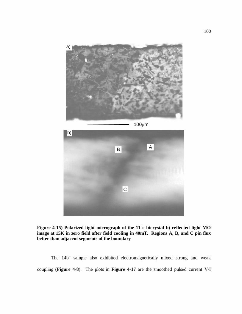
100
AB
C
a)
b)
100µm
Figure 4-15) Polarized light micrograph of the 11°°c bicrystal b) reflected light MOimage at 15K in zero field after field cooling in 40mT. Regions A, B, and C pin fluxbetter than adjacent segments of the boundary
The 14b° sample also exhibited electromagnetically mixed strong and weak
coupling (Figure 4-8). The plots in Figure 4-17 are the smoothed pulsed current V-I

101
traces for this sample, and they exhibit clear signs of parallel weakly and strongly coupled
components, the strongly coupled component being the minority component with the field-
independent trace. In Figure 4-16, the polarized light micrograph of 14°b is adjacent to
the MO image of 14°b that was field cooled in 400mT to 8K. Darker represent areas of
higher flux concentration. The MO image shows that flux preferentially entered the
boundary except for a bridge ~15µm wide which resisted flux entry in a manner similar to
that of the intragranular regions. However, this strong pinning bridge does not appear to be
a related to any specific macroscopic feature of the GB.

102
a)
b)50µm
Figure 4-16) a) Polarized light micrograph of the GB in sample 14°°b. b) Magneto-optic image of the same region. The image was taken after being field cooled to 8K in40mT.

103
0 100 200 300 400 500
0
10
20
30
40
V(µ
V)
I(mA)
0 50 100 150
-2
0
2
4
5mT
10mT
25mT50mT
0mT
200mT
100mT
WEAKLY COUPLED
COMPONENT
STRONGLY COUPLED
COMPONENT
Figure 4-17) Smoothed data from pulsed V-I traces on 14°°b as a function of magneticfield. There is a sharp decline in the Ic in low magnetic fields, but the inset highlightsa far less field-dependent Ic.
These MO images are consistent with an increase in electromagnetic coupling
inhomogeneity as the misorientation angle increases. They also suggest that macroscopic
regions of this inhomogeneity can be imaged. It is not clear whether these bridges are

104
macroscopically homogeneous or whether they contain a higher density of much smaller,
strongly coupled bridges than the relatively weaker segments of the boundary. It should
also be noted that MO images are most sensitive to the surface layer, thus the through-
thickness behavior is not clear from the images.

105
Results - Role of the Macroscopic Grain Boundary Plane
The influence of the macroscopic GB plane was specifically investigated for the 7°,
11° and 38° bicrystals. The 7° bicrystal had a slowly curving and a step-like portion to the
boundary. It was laser cut into two sub-samples 7°a and 7°b, 7°a having the smoothly
varying boundary and 7°b having the step-like boundary (Figure 4-18). The normalized
Jc(g.b.)/Jc(grain) behavior of the step-like boundary 7°b is a little more field dependent than 7°a
at low fields but the behavior is very similar above ~100mT (Figure 4-19).
I
100µm
a b
Figure 4-18) Polarized light micrographs of sample 7°°a and 7°°b. The grain boundaryin 7°°a is curved while the GB in 7°°b has two ~90°° kinks. Applied current direction isalong the long sample dimension as indicated.

106
B(mT)
0 200 400 600 800 1000
J c(g.
b.)/
J c(gr
.A)
0.0
0.1
0.2
0.3
0.4
0.5
0.6
0.7
0.8
0.9
1.0
7oa
7ob
Figure 4-19) A plot of the ratio of the intergranular Jc(B) vs. the lower intragranularJc(B) for samples 7°°a and 7°°b at 77K.
The 11° bicrystal, which had a smoothly curved GB, was subdivided into 3 sub-
samples: 11°a, 11°b, and 11°c. Bicrystals 11°a and 11°b had similar GB planes, which
were inclined at ~ 45° to the direction of current flow (Figure 4-20a, Figure 4-20b), while
the boundary plane in 11°c was nearly normal to the direction of current flow (Figure 4-

107
20c). The GB plane in these 3 sub-samples was essentially parallel to the surface normal.
Jc(g.b.)(B) of all three sub-samples were very similar, Jc(g.b.) exhibiting a decline of ~70-85%
in fields of ~20mT (Figure 4-21). Starting from a zero field value of ~104A/cm2, all sub-
samples exhibited a similar residual supercurrent of 1-2 x 10³ A/cm2, which was
independent of field in the measured range of 20 to 400mT.
I
a b c
100µm
Figure 4-20) Polarized light micrographs of samples 11°°a, b, and c. The boundaryplanes in 11°°a and 11°°b have similar inclinations to the samples’ long axis, while 11°°cis nearly normal to the long axis. Applied current direction is along the long sampledimension as indicated.

108
B(mT)
0 100 200 300 400102
103
104
105
11oc11ob11oa
J c(A
/cm
2 )
0 5 10 15 20 25
103
104
Figure 4-21) Plot of the Jc(B,77K) characteristic for samples 11°°a, b, c.
The 38° bicrystal was sectioned into 5 sub-samples, 38°a through e. Samples
38°a-d were polished to ~85µm thickness and laser cut as were the previous samples.
Sample 38e° was kept as a massive sample which was as wide as the sum of 38°a-d
(~1.5mm) and was 0.5mm thick. The much larger 38°e sample had a sufficiently large
enough Ic(H) that it was possible to measure extended V-J curves at high fields. Sample

109
38°b cracked and was not measured; the other sub-samples had the boundary inclinations
indicated in Figure 4-22. Four sub-samples were measured (38°a, c, d and e). Their
Jc(g.b.)(77K, 0mT) values were strongly depressed to ~60-150A/cm2, as compared to the
5,000-10,000A/cm2 of the smaller misorientation bicrystals. Weak fields of even 1mT
depressed the Jg.b. of all sub-samples to below 0.1A/cm2.
a c d
I
100µm
Figure 4-22) Polarized light micrographs of samples 38°°a, c, d showing the differentgrain boundary plane inclinations. Current direction is along the long sampledimension.
In summary, we found that macroscopic boundary plane effects were small for 7°,
11° and 38° bicrystals and, where present, not obviously distinguishable from small effects
introduced by the different self-fields of different samples. It is also noted that the effect
of the macroscopic grain boundary plane is dwarfed by the effect of the general
misorientation angle. This is not in contradiction to the magneto-optic results, which do
show inhomogeneity of the GB plane, but at the 10µm size scale or below. The

110
macroscopic grain boundary plane experiment could not probe variations at this fine of a
size scale.

111
Discussion
Taken as a whole, the data presented shows that the transition from strongly-coupled
to weakly-coupled for bulk scale, melt-textured YBCO bicrystals of general misorientation
is neither abrupt nor complete as one progresses from a low (5°) to high angle (38°) grain
boundary. The characteristics taken into account in judging the electromagnetic character
of the GB are the magnitude of the zero field critical current density, the field-dependence
of the critical current density, and whether or not the extended V-J characteristics show a
low-voltage, vortex-glass-like transition comparable to that seen within the grains. By
these criteria it is clear that the 5° bicrystal is fully coupled. There is a distinct and
progressive increase in the field dependent Jc (77 K) as θ increases, culminating in the
extreme field dependence of the very high angle bicrystal (38°), but even this GB showed
evidence of the irreversibility field transition at the same magnetic field as the intragranular
regions. Thus it appears that a small, but nevertheless finite, strongly coupled section of
GB remains, even at very high angles.
Systematic information about the misorientation dependence of the properties of GBs
has come mainly from thin films grown on bicrystal substrates. In the original thin film GB
misorientation studies [14,139,140], [001] tilt boundaries in YBCO showed a rapid fall in
the ratio Jc(g.b.)/Jc(grain) as θ increased beyond 5°. Indeed, even a 5° [001] tilt boundary
exhibited asymmetric I-V curves and extreme field sensitivity, indicating that it was weakly

112
coupled. In the limit of low θ, [001] tilt GBs can be described as heterogeneous interfaces
containing lattice dislocations which run from top to bottom of the film and lie parallel to
each other in the GB. The dislocations are separated by channels of comparatively
undisturbed lattice. Thus it is natural to explain the transition from strong to weak coupling
of [001] tilt GBs in terms of the narrowing of the undistorted channel with increasing θ,
either because the dislocation cores[14] or their strain fields overlap[15]. Implicit in this
model is the idea that the dislocation core is not superconducting and that supercurrent is
confined to the channels between the cores, or to proximity coupled regions adjacent to the
dislocation cores. In the limit of θ < 3-5°, this model is quite plausible because it associates
the strongly coupled electromagnetic properties to the comparatively undisturbed channels
that lie between the dislocation cores.
To explain the electromagnetic properties at higher angles, this basic model can be
generalized, as is schematically illustrated in Figure 4-23. The simple dislocation-core
model is shown in Figure 4-23a for both open (left) and closed (right) configurations [14].
When the dislocations or their strain fields overlap, the boundary becomes weakly coupled
since the cores are normal or insulating. The ohmic nature of the higher voltage portions of
the V-J curves in Figure 4-10 and Figure 4-12 argue that the cores are normal. The
second scheme is a modification of the first in that the coupling strength of the weakly
coupled GB lying beyond the overlap misorientation is itself spatially modulated. Sarnelli
et al. [141] proposed that the residual supercurrents observed at high fields in higher angle
thin film GBs were characteristic of transport through a set of parallel Dayem bridges
(Josephson-coupled regions separated by normal barriers) (Figure 4-23b). A third, more

113
general possibility is that high angle GBs of general misorientation still contain a few
strongly coupled paths[142, 143, 128, 37, 144] (Figure 4-23c), even though the majority of
the GB is weak-linked. Potential sources of the strongly coupled paths might be infrequent
structural units that are strongly coupled regions of matched lattice between widely spaced
dislocations, or symmetric facets with no hole depletion across them[145]. This model can
rationalize the rapid fall off of Jc in low fields as being due to field-induced destruction of
the majority, proximity-coupled part of the GB, while the higher field, residual
supercurrent occurs by transport through the (minority) strongly coupled regions. At what
misorientation angle, and for what type of bicrystal, any of these models are accurate is
subject to debate. The Dimos et al. data are consistent with a transition near 5°[13] to
10°[14], while the more recent and complete data set of Heinig et al. [146] suggests that
the channels [14,15] close between 10 and 15°. Differences between the two studies may
be at least partially ascribed to differences in the growth conditions of the films and the
influence that this has on the effective dislocation core size. Consistent with the higher
angle transition of Heinig et al.[146], Babcock et al.[4] found strong coupled behavior in a
14° [001] tilt, bulk YBCO bicrystal and Cai et al.[147] found that H*(GB)~H*(grain) up to
at least 18° [001] tilt, also finding the large GB resistance at higher voltages similar to that
seen in Figure 4-12 for the 38° bicrystal. Suhara et al.[148] found the transition from
strong to weak coupling to be between 10° and 15° for Tl-1223 and Tl-2212 thin films.
Thus it seems clear that the channel model seems to be a good basis for understanding the

114
crossover from strong to weak coupling, at least for [001] tilt bicrystals, but also that the
exact position of the crossover is sample- and perhaps material-dependent.

115
WEAK S/C, JJCHANNELS
NORMAL OR INSULATINGDISLOCATION CORES
b) Dayem Bridge Model(θ>∼15o −20o)
NORMAL ORINSULATINGDISLOCATION CORES
STRONG S/CCHANNELS
θ<∼5o-10o
CORE OVERLAP:TUNNELINGBARRIER
a) Dimos Model
θ>∼5o-10o
NORMAL OR INSULATING DISLOCATION CORE
STRONG S/C CHANNELS
PROXIMITY COUPLEDREGION
c) UW TF(θ<~20o)
Figure 4-23) Schematic drawings of three models for explaining the GB Jc in thin film[001] tilt YBCO as a function of GB structure: a) The dislocation core model [14,15],before and after core overlap, b) The Dayem bridge model[141], and c) Two channelmodel[42,146].

116
One source of the strongly coupled regions within the GBs is suggested by the recent
analysis of dislocation structure of [001] tilt flux grown bicrystals by Tsu et al.[149], which
shows that dislocations are neither uniformly spaced, nor of one type and that
macroscopically straight grain boundaries facet on the scale of tens of nanometers. Such
boundaries have variable width channels, thus naturally leading to residual, high field
supercurrents being present at higher angles than would occur for equally spaced
dislocations. In the melt-textured, general (or “mixed”) misorientation bicrystals, we have
an even more complicated situation. Whereas [001] tilt boundaries in principle have only
one set of dislocations, a mixed misorientation GB has at least three intersecting sets of
dislocations. This changes the shape of the strongly coupled channels in the GB plane from
extended rectilinear objects sandwiched between parallel dislocation sets (Figure 4-24a) to
point-like contacts in mixed misorientation grain boundaries[150] (Figure 4-24b). The
mixed misorientation sketch is based on recent electron microscopy studies of low angle
MOMT GBs by Miranova et al.[150] (the dislocation cores are black, the associated strain
field is gray, and undisturbed lattice is white). The provocative result of the present work
is that such mixed misorientation boundaries still show evidence of strongly coupled paths,
in spite of the much smaller areas of “strong” channel that are expected from the model.
The evidence for this conclusion lies both in the electromagnetic results and from the
magneto-optic imaging on the 5°, 11° and 14° boundaries, which provided visual evidence
of strongly coupled channels across the GB. Perhaps the combination of macroscopic and
microscopic facetting allows for a large number of possible dislocation spacings, of which
some may allow small, strongly-coupled gaps.

117
a)
d
b)
Figure 4-24) Schematic representations of the possible microstructure viewed in theGB plane (GB normal is out of the paper) of a) the prison bar model of a simple [001]tilt boundary. The black regions are the dislocation cores, the gray are the areas nearthe cores that are degraded due to strain, while the white areas represent undisturbedlattice. Note the large 2-D rectangular regions of this undisturbed lattice. b) Generalmisorientation GB, composed of a grid of 4 sets of dislocations, results in ageometrical network of essentially point, rather than line contacts (adapted fromMiranova et al.[150]).
Figure 4-25 is a plot of the Jc(g.b.)(θ, B=0) values for the mixed misorientation, melt-
textured, samples described in my work[22,33,151], as well as values for flux-
grown[20,152], seeded melt-textured[93], and thin film YBCO bicrystals[146,153] found
in the literature. It is clear that the intragranular regions of thin film bicrystals have far
higher Jc(g.b.)(θ,B=0) values than bulk melt-textured or flux-grown bicrystals, but that the
drop off of Jc(g.b.)(θ,B=0) is significantly sharper for the thin films. So different are the
angular dependence of the two classes that the absolute Jc(g.b.) values crossover at ~35°. In

118
contrast, the bulk Jc(g.b.)(θ, B=0) values are rather flat out to ~10° and a very gradual drop-
off of Jc(g.b.)(θ, B=0) despite the far more complicated misorientations (and hence
dislocation structure) of many of the bulk scale bicrystals!
General Misorientation θ
0 10 20 30 40 50 60 70
J c(A
/cm
2 )
101
102
103
104
105
106
107
77K
Figure 4-25) Plot of the Jc(g.b.)(B=0, 77K) values for flux-grown ([20,152]), melt-textured (UW/AT&T MT - [22], MOMT - [33], UW MT - [22], Boeing seeded -
[151], Argonne seeded - [93]) and thin film (Ivanov et al. - zz[153], Heinig et al. -[146]) bicrystals, as a function of general misorientation angle.

119
I have plotted in Figure 4-26 the ratio of the intergranular (from Figure 4-25) to
intragranular Jc(B=0) of the previous bulk and thin film bicrystals in the manner of Dimos
et al.[14]. For many samples, both the inter- and intragranular Jc values were measured
(the solid white and black symbols). In other samples, the intragranular regions were too
small to measure by transport and had to be estimated based on well established
intragranular values of similar samples (the symbols with white crosshairs). For melt-
textured samples, the estimated intragranular Jc(0T, 77K) was 2.5 x 10⁴A/cm2 (this is
generally accurate to within a factor of 2). For [001] tilt flux-grown bicrystals[152], the
intragranular Jc(0T, 77K) was estimated at 4000A/cm2[4]. Plotting the data as a ratio re-
emphasizes the disparity of zero field boundary behavior as a function of misorientation
between the bulk scale and thin film samples. For example, at 30°, the Jc ratio of bulk
bicrystal boundaries has fallen by ~1-2 orders of magnitude, but for thin film boundaries it
has fallen by 3 orders of magnitude. However, one must use caution in interpreting zero
field GB critical current densities since they may be sensitive to self-field effects and to
extrinsic factors, such as cracks, which are common in bulk samples.

120
General Misorientation θ
0 10 20 30 40 50 60 70
J c(g
.b.)/J
c(gr
ain
)(B=0
)
10-4
10-3
10-2
10-1
100
THIN FILM
BULK
Figure 4-26) Plot of the ratio of the intergranular to intragranular critical currents(0T, 77K) for melt-out samples (z, ), in comparison to other general misorientation,UW melt-textured samples previously measured at 77K( )[22],()[151], Argonneseeded melt-textured bicrystals ( )[93], UW/NIST [001] tilt bulk flux-grownbicrystals at 77K( )[20,152], thin film samples of mixed misorientation at 5K() byDimos et al.[14], [001] tilt thin film samples at 77K() by Heinig et al.[146], and [001]tilt thin film samples at 77K(∆∆) by Ivanov et al.[153]. Symbols with white crossesindicate that the intragranular Jc was estimated, while all other samples hadmeasured intragranular Jc values. Second order regression fits to all the bulk scaleand thin film data illustrate that bulk scale grain boundaries tend to have a weakerdecline of Jc(g.b.) with increasing misorientation angle than the thin film boundaries.

121
An important issue not always considered in studies of the misorientation
dependence of the Jc is the field-dependence of the properties. An example of the fact that
the zero field and in-field properties are not the same is illustrated in the four plots of
Figure 4-27. Transport data for bicrystal 7°a were taken inside both grains, as well as
across the boundary for the conditions where B was both ~||c and ~⊥c. Considering the
whole Jc(g.b.)(B) characteristic gives a more complete picture of the electromagnetic role of
the GB. When data is plotted as Jc(g.b.)(B)/Jc(grain)(B) in Figure 4-27b and d, a line with zero
slope indicates strong coupling, a steep negative slope indicates weak coupling, and a
positive slope indicates that the intragranular Jc is declining more rapidly than the
intergranular Jc. The vertical axes in Figure 4-27b and d define the effectiveness of the
boundary in passing supercurrent. About 40% of the weaker grain’s supercurrent is
transported across the boundary in zero field, but this fraction increases sharply to ~1 for
fields ~⊥c up to 1T, before settling at ~0.7 from 2T to 8T (Figure 4-27b). Thus there does
appear to be a proximity-coupled component to the supercurrent transport at low fields,
indicating some weak link behavior to the GB. However, the boundary does not act as a
weak link at 1T, and is only a minor impediment at higher fields. For H~||c, there is also a
strong weak link effect in low field (<20mT), Ic(g.b.)/Ic(grain) decreasing from about 0.7 to 0.3
before rebounding to ~0.8 and then decreasing to zero at H* (Figure 4-27d). Plotting the
data in this manner shows that, despite some low magnetic field sensitivity, this 7°
boundary is not a severe impediment to the high field critical current. This result may help
to explain the recent good transport Jc values (~2.5x10³A/cm2, 77K) in high magnetic fields
(0-3T) found in magnetically aligned YBCO thick films[29], whose grains are believed to

122
be generally misorientated by ~10°[31]. The result is also consistent with the recent study
of Wang et al. on a BSCCO-2212 8° [001] tilt bicrystal[154]. When tested at fields up to
H*, they both showed that the GB could transmit large fractions (~75%) of the
intragranular current. Therefore it seems desirable to consider the magnetic field-
dependent properties of grain boundaries and not just the self field properties in considering
the full character of grain boundaries and their influence on the transport current

123
H(T)
0 1 2 3 4 5
I c(g
.b.)/I c
(gra
in)
0.0
0.1
0.2
0.3
0.4
0.5
0.6
0.7
0.8
0.9
1.0
H(T)
0 1 2 3 4 5 6 7 8
I c(g
.b.)/I c
(gra
in)
0.0
0.1
0.2
0.3
0.4
0.5
0.6
0.7
0.8
0.9
1.0
c)
b) d)
vs. Grain A
vs. Grain B
vs. Grain A
vs. Grain B
B~⊥c B~||c
H(T)
0 1 2 3 4 5 6J c(
A/c
m2 )
102
103
104
105
cross-boundary
grain B
grain A
B~||c
H(T)
0 1 2 3 4 5 6 7 8
J c(A
/cm
2)
102
103
104
105
cross-boundary
grain Bgrain A
B~⊥c
a)
Figure 4-27) Plots of the ratios of the intergranular to intragranular critical currentsas a function of applied magnetic field at 77K: a) Jc(B) for the inter and intragranularregions of sample 7°°a with B~⊥⊥c, b) The ratio of intergranular I c to intragranular I c
with B~⊥⊥c, c) Jc(B) for the inter and intragranular regions of sample 7°°a with B~||c,d) The ratio of intergranular I c to intragranular I c with B~||c.

124
Chapter 5 : Summary and Conclusions
The fundamental conclusion of this thesis is that the transition from strong to weak
coupling in bulk scale, melt-processed YBCO is neither abrupt nor complete as a function
of increasing general misorientation. My original, conventional voltage level data on high
angle boundaries (15°-69°) already suggested that there was a smooth transition from
strong to weak coupling and that strongly-coupled paths (at least at 4K), existed for all high
angle boundaries. My more recent high sensitivity transport data show more clearly that
both transition angle (θ=7°-11°) and high angle (θ=38°) grain boundaries have minority,
strongly coupled paths, even at 77K. The residual critical current seen at high magnetic
fields appears to have a flux-pinning nature, as evidenced by the observation that the
irreversibility line measured across the grain boundary is about the same as in the grains.
This observation is bolstered by magneto-optic imaging, which was used to directly observe
inhomogeneous coupling on a scale of ~10µm in the 11° and 14° GBs.
The effect of the macroscopic grain boundary plane on the overall electromagnetic
character of a melt-out melt-textured grain boundary was found to be minimal, supporting
my initial assumption that the crystal misorientation angle is the key parameter of the full
grain boundary misorientation description for determining superconducting properties. The
results of the magneto-optic imaging and the subsection of the grain boundary plane
experiments are not necessarily contradictory, as these two experiments investigate

125
different size scales. The macroscopic grain boundary plane experiment probed the grain
boundary plane on the scale of several hundred microns, more than an order of magnitude
greater than the features seen in the magneto-optic images. It is also worth noting that the
stronger coupled regions in the magneto-optic image do not require that the material is
homogeneously strongly-coupled (this would be incompatible with any dislocation model
of the grain boundary), but rather that it has a higher density of strongly-coupled elements
than the other regions of the grain boundary.
The angular dependence of the ratio of inter- to intra-granular critical current for
melt-textured bicrystals was found to be similar to that in bulk scale flux-grown bicrystals
but less severe than in thin film bicrystals. However, this ratio depends on the applied
field, becoming larger in higher fields (~>1T), thus showing that the GB weakens less than
the grain under increasing field.
Finally, it is interesting to ascertain whether the bulk or TF bicrystals serve as a
better model for the grain boundaries in the extremely promising Ion-Beam Aided
Deposition (IBAD) tapes. It is unclear whether the IBAD grain boundaries should be
considered thin film or bulk in nature, as the tapes are deposited via a thin film technique
but have thicknesses more usually associated with the bulk (some IBAD tapes are as thick
as 9µm). Although IBAD tapes cannot be tested as bicrystals, we can correlate their Jc
properties with bicrystal data by correlating Jc to the FWHM of the (103) pole figure. This
pole figure has components of both c and ab pole misorientation, and so is analogous to a
general misorientation angle. Using a summary of IBAD data from Freyhardt et al.[155],
and estimating the intragranular Jc to be 2 x 10⁶A/cm2 (a reasonable value obtained from

126
intragranular regions of TF YBCO[152]), a collection of intergranular vs. intragranular Jc
ratios can be obtained. This data can be compared to experiments on TF bicrystals (Figure
5-1) and bulk scale bicrystals (Figure 5-2). Although it is clear from very recent
experiments of my colleague A. Pashitiski[156] that the current path in IBAD tapes is
controlled by percolation, still, it is interesting to note that the IBAD data follows well the
data for bulk scale bicrystals for essentially the entire angular range. Therefore, future
studies of bulk scale bicrystals (MT or FG) may have special relevance to the attempts to
refine and improve IBAD tapes.

127
General Misorientation θ (degrees)
0 10 20 30 40 50 60 70
J c(g.
b.)/J
c(gr
ain)
(B=
0)
10-3
10-2
10-1
100
Figure 5-1) Plot of the estimated Jc(g.b.)/Jc(grain)(77K) ratios at zero field for IBAD tapes(z)[155] vs. thin film (TF) bicrystals ()[146,153]. The intragranular Jc value forIBAD tapes is estimated at 2X10⁶A/cm2, a standard YBCO TF value[152]. The IBADratios are consistently higher than the TF ratios above 10°°.

128
General Misorientation θ (degrees)
0 10 20 30 40 50 60 70
J c(g.
b.)/J
c(gr
ain)
(B=
0)
10-3
10-2
10-1
100
Figure 5-2) Plot of the estimated Jc(g.b.)/Jc(grain)(77K) ratios at zero field for IBAD tapes(z) vs. bulk bicrystals (, flux grown[20,152] and melt-textured[22,151,93]). TheIBAD ratios lie among the bulk bicrystal ratios.

129
In summary:
Melt-textured bulk scale bicrystals have been successfully isolated and
characterized in detail.
The change from strong to weak coupling as a function of misorientation angle
is neither abrupt nor complete. There exists a transition region, ~7°-20°, that
contains significant fractions of both weak and strong coupling.
Evidence has been provided to support the concept that the high field residual
current is due to minority, strongly coupled components of the grain boundary.
Melt-textured bulk scale bicrystals have shown to be possible models for the
misorientation dependence of IBAD tapes.

130
Appendix A: The Mixed Misorientation Description
The Mixed Misorientation Description - General Grain Boundary
Geometry
There are five macroscopic degrees of freedom associated with a complete
description of the misorientation of the two grains and the boundary that form a general
bicrystal.[131] There are two basic schemes for describing these five degrees of freedom;
the interface-plane scheme, which describe the misorientation in terms of the lattice planes
at the grain boundary, and the misorientation scheme, which describes it on the basis of the
two crystallographic lattice orientations. The basis of this appendix is the latter, more
common scheme. Of the five degrees of freedom needed to describe the grain boundary,
two degrees describe the boundary plane normal n (two independent direction cosines),
two describe the rotation axis u (two independent direction cosines) and one is needed to
describe the rotation angle that sets both crystals coincident (Figure A-1).

131
c
a
b
c’
b’
a’GRAIN BOUNDARYNORMAL n
c
b
a
c’
b’
a’
GRAIN BOUNDARYNORMAL n
ROTATION AXIS u
ROTATION ANGLE θ
a)
b)
Figure A-1) a) Schematic drawing of a general misorientation grain boundary with aflat grain boundary plane. b) The misorientation between crystal abc and a’b’c’ in a)can be described by a rotation angle θθ about a rotation axis u that sets both crystalcoincident. The grain boundary normal n is independent of θθ and u.

132
There are two popular ways of describing the crystallographic misorientation - by a one
angle/axis pair method, or by three Euler angles. The one angle/axis pair description of
grain boundary misorientation was originally promoted by Lange[131], and it is presently
the preferred description in the crystallography and microscopy communities. The
complete description is the rotation angle θ about the rotation axis [UVW] with the grain
boundary normal n. The values for the rotation angle and axis are derived from the
misorientation matrix, M , which is obtained from experimentally determined data of the
misorientation between low index poles of the two crystals. The elements of the
misorientation matrix are direction cosines between the low index poles of one crystal with
the low index poles of the other crystal, i.e. a 3 x 3 matrix of direction cosines:
M =
cos cos cos
cos cos cos
cos cos cos
' ' '
' ' '
' ''
θ θ θθ θ θθ θ θ
aa ab ac
ba bb bc
ca cb cc
where the axes of crystal 1 are a, b, c and crystal 2 a′, b′, c′
The axis of misorientation (UVW) and the angle of misorientation (θ) about this axis can be
extracted from the matrix by the following formulae:
cos (cos cos cos ) /
: : cos cos cos cos :cos cos
' ' '
' ' : ' ' ' '
θ θ θ θθ θ θ θ θ θ
= + + −= − − −
aa bb cc
cb bc ac ca ba abU V W
1 2
(if θ=180°, U V W a a a: : ( ) :( ) :( )= + + +11 22 331 1 112
12
12 )

133
For misorientations about low index poles, twist and tilt terms can be used to
further describe the boundary (Figure A-2). A twist boundary is one in which the grain
boundary plane normal is parallel to the rotation axis. A tilt boundary is one in which the
grain boundary plane is orthogonal to the rotation axis. If we describe the rotation angle as
θ, the angle between the rotation axis u and the grain boundary normal n as α, than the
twist angle (φ) and tilt angle (ω) can be described as such:
sinsin
( tan cos
sin sin sin
φθ
α θ
ω α θ
22
12
2 2
2 2
=+
=
It should be stressed that this decomposition into twist and tilt angle components cannot be
done if n is not precisely defined and constant for the boundary area under analysis.

134
c
a
b
c’
b’
a’
rotation axis u
grain boundary normal n
c
a
b
c’
b’
a’
rotation axis u
grain boundary normal n
tilt:u⊥n
twist:u||n
a)
b)
Figure A-2) a) Drawing of a tilt grain boundary: the rotation axis is perpendicular tothe grain boundary plane normal (u⊥⊥n). b) Drawing of a twist grain boundary: therotation axis is parallel to the grain boundary plane normal (u||n).

135
The Euler angles description is preferred in the physics community.[157] Any
misorientation may be described by three consecutive rotations about three orthogonal
axes. There are many different choices of rotations allowed, but a popular convention used
in mechanics and solid state physics is illustrated in Figure A-3. The first rotation is Ψ
about z, the second Θ about x′′, and the last is Φ about z′. This results in the following
relation to the measured misorientation matrix M:
M =
=
− +− − − +
−
cos cos cos
cos cos cos
cos cos cos
cos cos sin sin cos cos sin cos cos sin sin sin
cos sin cos sin cos sin sin cos cos cos cos sin
sin sin sin cos cos
' ' '
' ' '
' ''
θ θ θθ θ θθ θ θ
aa ab ac
ba bb bc
ca cb cc
Ψ Φ Φ Ψ Θ Ψ Φ Θ Φ Ψ Ψ ΘΦ Ψ Θ Φ Ψ Ψ Φ Θ Φ Ψ Ψ Θ
Θ Φ Θ Φ Θ
Using the above relation, one can solve for the Euler angles Φ, Θ, and Ψ.

136
Figure A-3) Graphical definition of the Euler angles (ΘΘ, ΦΦ, and ΨΨ). Themisorientation between two crystals of axes xyz and x’y’z’ can be described by arotation about z, followed by a rotation about x’’, and then a rotation of about z’.Figure adapted from Randle[118].
No matter what misorientation description is used, there are a number of
crystallographically equivalent rotation matrices M ′, the number of such matrices
depending on the symmetry of the crystallographic system. These matrices will result in
several equivalent angle/axis combinations.
M ′′=TiM
where Ti are the symmetry operation matrices and i=1 to n (n=1+n2+2n3+3n4+5n6), where
n2 is the number of two fold symmetry axes, n3 is the number of threefold symmetry axes,
etc.

137
Since YBa2Cu3O6+x is approximated as tetragonal (a~b and the samples are twinned), there
are four two-fold symmetry axes (about [010], [100], [11 0], and [110]) and one four-fold
symmetry axis (about [001]), resulting in eight symmetrically equivalent rotation matrices
M ′. The individual Ti rotation matrices are:
1 0 0
0 1 0
0 0 1
1 0 0
0 1 0
0 0 1
1 0 0
0 1 0
0 0 1
1 0 0
0 1 0
0 0 1
0 1 0
1 0 0
0 0 1
0 1 0
1 0 0
0 0 1
0 1 0
1 0 0
0 0 1
0 1 0
1 0 0
0 0 1
, , , , , , ,
By convention the angle/axis pair with the smallest angle is sometimes called the
disorientation angle and this angle/axis pair is used to describe the bicrystal misorientation.
The Mixed Misorientation Description - Example
Here is an example showing how raw x-ray pole figure data are converted into a
axis/angle pair description of the misorientation. The x-ray data for sample MB4C1 was
taken as described in Chapter 3. Figure A-4 shows this data plotted on a stereographic
projection with the aid of a Wulff net (Figure A-5), a device used in solving stereographic
projection problems.[158] The Wulff nets used in my work, with a diameter of 18cm, are
accurate to ~1°.

138
Pole Figure Data for Sample MB4C.1
0
30
60
90
0 30 60 90
0
30
60
90
03060900
90
180
270
crystal 1crystal 2
c
c'
a/b
a/b
a/b'
a/b'
Figure A-4) Pole figure data plotted on a stereographic projection, with each point acentroid of the labeled pole. The orthorhombic structure of YBCO constrains whichpole belongs to which crystal.

139
Figure A-5) A Wulff net, used to measure angles from a stereographic projection.The longitudinal lines are known as the “great circles.”
Measurements of each element of the matrix are accomplished by rotating two poles of
interest on the stereographic projection so that the two poles are coincident on the same
“great circle”, like the c-axis poles for each crystal in Figure A-6. The cosine of the angle

140
between these poles on the same great circle form a matrix element. Finding the angular
relationship between all poles allows us to build the misorientation matrix:
M =
cos cos cos
cos cos cos
cos cos cos
51 67 47
128 38 82
113 124 44
o o o
o o o
o o o
cosθ=(0.6293+0.7880+0.7193-1)/2
∴θ=55°
U:V:W=-0.6984:1.073:-1.0064
This UVW ratio would be the ratio of the Miller indices only in the cubic case. In order to
get the axis ratio in terms of Miller indices, we need to multiply the U and V values by 3 for
YBCO (c~3a,b).
U:V:W~15:23:7 ~2 :3:1
Performing the symmetry operations resulted in a series of matrices that all happened to
have a smaller trace than the original matrix, which means the original matrix had the
smallest θ. Therefore the disorientation angle/axis pair for the MB4C1 bicrystal is
described as 55°[ 2 3 1 ].

141
Pole Figure Data Rotated to Measure c-c' Angle
20 50 80
20
50
80
205080
20
50
80
0
90
180
270
crystal 1crystal 2
c' c
a/b'
a/b'
a/b
a/b
41o
Figure A-6) The poles marked on Figure A-4 are rotated so that the c’ and c poles lieon the same great circle. Then the misorientation angle between c and c’ can bedetermined by noted the angular distance on the great circle (θθcc’=41°°).

142
Appendix B: Laser Cutting of YBa2Cu3O6+x
The fracture technique for bicrystal isolation resulted in only low yields of
measurable bicrystals from a given batch of starting material. Many of these were of such
small size that it was difficult to perform x-ray pole figures and to apply contacts for
electrical experiments. Melt textured samples often have large grains, on the order of
millimeter size. If mm-scale bicrystals could be isolated, x-ray pole figure data collection
would be greatly simplified, and contacting would be eased to the extent that it would now
be practical to apply intragranular as well as intergranular, contacts to the samples. Cutting
samples with a finely focused laser beam seemed to be a promising solution; Schindler et
al.[36] had showed that individual grain boundaries in sintered Dy-123 could be isolated
with the aid of a laser cutter.
Lasers with different wavelengths have different material interactions. Excimer
lasers, used in the laser deposition of high Tc films, have a short wavelength and remove
material by the process of ablation. Ablation is the name of the process whereby
ultraviolet photons break the chemical bonds on the target, decomposing the compound
into its constituent molecular components. This procedure results in little heating to the
adjoining regions. By contrast, solid-state lasers, like Nd:YAG (Nd+3 doped Y3Al5O12 ), or
frequency doubled or tripled Nd:YAG, have a long wavelength (in the visible or infrared
region) and remove material by the process of thermoevaporation. Thermoevaporation
involves the local heating of the material through the solid-liquid-gas transitions until the

143
material is ejected (Figure B-1)[159] from the incident beam region. With a
thermoevaporative process, it is required that the material have low thermal diffusivity in
order to keep the beam energy localized so as to facilitate cutting and to prevent heat
damage to the adjoining regions. This is a large part of the reason why infrared lasers are
more effective at cutting ceramics than metals. Another is that metals easily reflect the
incident laser beam.
Figure B-1) Schematic drawing of the thermoevaporation process from ref.[159].Laser beam first melts the material and then heats the liquid until the vapor phase isformed and ejected from the cut.
The amount of laser energy absorbed by YBCO as a function of wavelength has
been investigated with respect to Bouguer’s Law of absorption (Equation B-1)[160]. The

144
variable q is the radiation at depth z into the sample, q0 the initial radiation, R is the
reflectivity and α is the absorption coefficient:
Equation B-1
q z q R ez
( ) ( )= −−
0 1α
Table B-1: Bouguer’s constants for different laser wavelengths[160].
Laser Wavelength(µµm) αα(105cm-1) RCO2 ~10 0.5 0.75Nd:YAG 1.064 1.2 0.18Nd:YAG(freq. doubled) 0.533 1.5 0.14Nd:YAG(freq. tripled) 0.355 1.7 0.12XeCl(excimer) 0.308 1.9 0.12KrF(excimer) 0.248 2.3 0.13ArF(excimer) 0.193 2.4 0.15
From Table B-1 we see that except for the CO2 laser, the reflectivities (R) are
similar, so the absorption coefficient (α) is the key parameter. Clearly, the longer
wavelength is better, although the CO2 wavelength is so large that it is on the same order of
magnitude of the dimensions of the desired cut features. Some experimental evidence with
respect to YBCO film deposition has quantitatively shown that the infrared wavelength
couples better to YBCO than do the shorter wavelengths of excimer lasers (Figure B-
2)[161], thus allowing for more efficient removal of material.

145
Figure B-2) Plot of ablation depth per laser shot as a function of laser wavelength,from ref.[161].
Our requirements for a laser cutter, the ability to cut ceramic material 50-100µm
thick with a minimal cut width and damage region, but at a reasonable cost, led to a series
of lasers made for the semiconductor failure analysis industry. The lasers are mounted on
microscopes and are designed to remove passivation layers. Several lasers were tested for
their effectiveness in cutting sample YBCO material, including frequency doubled
Nd:YAG (λ=532nm) green lasers, as well as a Xenon (λ=480-520nm) and an infrared
Nd:YAG (λ=1064nm). Results varied, with some units cutting narrower, deeper and faster
than others. One laser, the infrared Nd:YAG, performed above the rest, as its high shot
frequency and infrared wavelength helped it cut faster. The final purchased laser was
manufactured by the Florod Co. It consisted of an Amoco solid state Nd:YAG pulsed
laser, two mirrors, a telescoping lens and an iris shutter that directed the beam vertically

146
through the microscope (Figure B-3). The laser operated at 1064nm with a pulse width of
15ns. The maximum power is 35mJ (max. energy density ~40J/cm2) out of the objective
with a variable pulse rate of 1 - 15000 Hz and a spot size of 2-20mm. This spot size was
adjustable by changing the telescoping ratio and by varying the shutter diameter. The laser
was fired through a long working distance Mitutoyo microscope which was mounted on a
Micromanipulator probe station. The X-Y stage of the probe station can be moved with
micron scale precision. The laser was selected for its ability to cut deep but narrow lines in
YBCO (it can achieve a steep-sided cut 80µm deep and 30µm wide).
M1M2
TelescopeAssembly
Iris
Tilt Plate
Laser
Front Interior Right Side
Figure B-3) Drawing of the Florod Nd:YAG laser, from the Florod LMSManual[162]. This assembly is mounted with the tilt plate attached to the top port ofa long working distance Mitutoyo microscope.

147
The possibility of laser damage to the bulk of the cut material was investigated.
The appearance of the material directly after cutting was discolored, (Figure B-4a). This
discoloration was not damage however. It was material ejected from the cut that had
settled on the surface. It could be removed by washing with methanol, which left behind
an extremely clean cut (Figure B-4b). Twins, which are very sensitive to local oxygen
concentration, could be seen in laser-cut samples right up to the cut edge. Thus the
damaged region may be estimated as no wider than the resolution of the microscope
(~1µm). Recent results in YBCO thick films cut with a Nd:YAG laser with two orders of
magnitude higher energy density had cut walls with a heat affected zone of 3µm[163].
Since the dimensions of our bulk samples are orders of magnitude larger than the largest
estimated size of the damage zone, we believe laser cutting to be an extraction technique
that does not effect the properties of our material.
100µma) b)
Figure B-4) An unpolarized light micrograph of a melt texture sample cut with a Nd-YAG laser a) before and b) after cleaning with methanol. The discoloration surroundthe cut in the first image is due to re-deposit material from the cut, and is not sampledamage.

148
As well as cutting melt-textured YBCO, the laser has proven effective in slicing
unsheathed BSCCO tape [164], as well as trimming flux-grown YBCO[147] and BSCCO
bicrystals.[154] Other groups outside the UW are currently using lasers to assist in the
electromagnetic investigation of bulk ceramic superconductors[38,165].

149
References
[1] M. K. Wu, J. R. Ashburn, C. J. Torng, P. H. Hor, R. L. Meng, L. Gao, Z. J. Huang,Q. Wang, and C. W. Chu, Phys. Rev. Lett. 58, 908 (1987).
[2] M. Suenaga, D.O. Welch, and R. Budhani, Supercond. Sci. Technol. 5, S1 (1992).
[3] M. Okada, A. Okayama, T. Morimoto, T. Matsumoto, R. Aihara, and S. Matsuda,Jpn. J. Appl. Phys. 27, 185-187 (1988).
[4] S. E. Babcock, X. Y. Cai, D. L. Kaiser and D. C. Larbalestier, Nature 347, 167(1990).
[5] K. Salama, V. Selvamanickam, L. Gao, and K. Sun, Appl. Phys. Lett. 54(23), 2352(1989).
[6] D. Shi, H. Krishnan, J.M. Hong, D. Miller, P.J. McGinn, W.H. Chen, M. Xu, J.G.Chen, M.M. Fang, U. Welp, M.T. Lanagan, K.C. Goretta, J.T. Duser, J.J. Picciolo,and U. Balachandran, J. Appl. Phys. 68(1), 228 (1990).
[7] T. Venkatesan, X.D. Wu, B. Dutta, A. Inam, M.S. Hedge, D.M. Hwang, D.M.Chang, L. Nazar, and B. Wilkens, Appl. Phys. Lett. 54, 581 (1989).
[8] G. Deutscher and K. A. Müller, Phys. Rev. Lett. 59, 1745 (1987).
[9] B. Oh, K. Char, A. P. Kent, M. Naito, M. R. Beasley, T. H. Geballe, R. H.Hammond, A. Kapitulnik, and J. M. Graybeal, Phys. Rev. B 37, 7861 (1988).
[10] A.K. Ghosh, M. Suenaga, T. Asano, A. R. Moodenbaugh, R. L. Sabatini, Adv.Cryogenic Mater. 34, 607 (1987).
[11] “Concise Encyclopedia of Magnetic and Superconducting Materials” ed. J.Evetts, Permagon Press, 415 (1992).
[12] T. Hikata et al., Jap J. Appl. Phys 28, L82 (1989).
[13] D. Dimos, J. Mannhart, P. Chaudhari, and F. K. LeGoues, Phys. Rev. Lett. 61,219 (1988).
[14] D. Dimos, J. Mannhart and P. Chaudhari, Phys. Rev. B 41, 4038 (1990).
[15] M.F. Chisholm, and S.J. Pennycook, Nature 351, 47 (1991).

150
[16] A.H. Cardona, H.Suzuki, T. Yamashita, K.H. Young, L.C. Bourne, Appl. Phys.Lett. 62(4), 411 (1993).
[17] M. Kawasaki, E. Sarnelli, P. Chaudhari, A. Gupta, A. Kussmaul, J. Lacey, andW. Lee, Appl. Phys. Lett. 62(4), 417 (1993).
[18] C. B. Eom, A. F. Marshall, Y. Suzuki, B. Boyer, R. F. W. Pease, and T. H.Geballe, Nature 353, 544 (1991).
[19] D.J. Lew, Y. Suzuki, A.F. Marshall, T.H. Geballe, and M.R. Beasley, Appl. Phys.Lett. 65(12), 1584 (1994).
[20] D. C. Larbalestier, S. E. Babcock, X. Y. Cai, M. B. Field, Y. Gao, N. F. Heinig,D. L. Kaiser, K. Merkle, L. K. Williams, N. Zhang, Physica C 185-189, 315 (1991).
[21] N Heinig, unpublished.
[22] M.B. Field, X.Y. Cai, S.E. Babcock, and D.C. Larbalestier, IEEE Trans. onSuperconductivity, Vol.3(1),1479, (1993).
[23] I.K. Yanson, Soviet Physics JETP 31(5), 800 (1970).
[24] L.N. Bulaevskii, J.R. Clem, L.I. Glazman, and A.P. Malozemoff, Phys. Rev. B45, 2545 (1992); L.N. Bulaevskii, L.L. Daemen, M.P. Maley, and J.Y. Coulter, Phys.Rev. B 48, 13798 (1993).
[25] S. E. Babcock, X. Y. Cai, D. C. Larbalestier, D.H. Shin, N. Zhang, et al., PhysicaC 227, 183 (1994).
[26] Y. Iijima, N. Tanabe, O. Kohno, and Y. Ikeno, Appl. Phys. Lett 74, 1905 (1993).
[27] X.D. Wu, S.R. Foltyn, P. Arendt, J. Townsend, C. Adams, I.H. Campbell, P.Tiwari, Y. Coulter, and D.E. Peterson, Appl. Phys. Lett. 65(15), 1961 (1994).
[28] A. Goyal, D.P. Norton, J.D. Budai, M. Paranthaman, E.D. Specht, D.M. Kroeger,D.K. Christen, Q. He, B. Saffian, F.A. List, D.F. Lee, P.M. Martin, C.E. Klabunde, E.Hatfield, and V.K. Sikka, preprint, (1996).
[29] J.A. Lewis, and M. Wegmann, Appl. Phys. Lett. 67(20), 3028 (1995).
[30] S.R. Foltyn, P. Arendt, X.D. Wu, W.R. Blumenthal, J.D. Cotton, J.Y. Coulter,W.L. Hutts, H.F. Safar, J.L. Smith, and D.E. Peterson, Extended Abstracts,MRS/ISTEC International Workshop on Supercondcutivity, Maui, HI, 1995.

151
[31] J.A. Lewis, ASC 96 Pittsburgh Poster Presentation (1996).
[32] A. Parikh, B. Meyer, and K. Salama, Supercond. Sci. Technol. 7, 455 (1994).
[33] M.B. Field, D.C. Larbalestier, A.S. Parikh, and K. Salama, Submitted to PhysicaC, (1996).
[34] Z. Yi, S. Ashworth, C. Beduz, and R.G. Scurlock, IEEE Trans. on Magnetics 27,1506 (1991).
[35] G. Schindler, B. Seebacher, and K. Andres, Journal of Less-Common Metals,164&165, 1346 (1990).
[36] G. Schindler, B. Seebacher, R. Kleiner, P. Müller and K. Andres, Physica C 196,1 (1992).
[37] C. Sarma, G. Schindler, D.G. Haase, C.C. Koch, A.M. Saleh, and A.I. Kingon,Appl. Phys. Lett. 64(1), 109 (1994).
[38] G. Schindler, C. Sarma, D.G. Haase, C.C. Koch, and A.I. Kingon, Cryogenics34(4), 287 (1994).
[39] C. Sarma, G. Schindler, D.G. Haase, C.C. Koch, A.I. Kingon and A. Goyal,Physica C 244, 287 (1995).
[40] D.W.A. Willén and K. Salama, Physica C 201, 311 (1992).
[41] M. Nilsson-Mellbin, A. Parikh, K. Salama, Physica C 223, 19 (1994).
[42] M.B. Field, A. Pashitski, A. Polyanskii, and D.C. Larbalestier, A.S. Parikh, andK. Salama, IEEE Trans. of Applied Superconductivity, Vol. 3(2), 1631, (1995)
[43] M.B. Field, A. Pashitski, A. Polyanskii, and D.C. Larbalestier, A.S. Parikh, andK. Salama, to appear in the Proceedings to the 10th Anniversary High TemperatureSuperconductor Workshop, (1996).
[44] S. Jin, T.H. Tiefel, R.C. Sherwood, M.E. Davis, R.B. van Dover, G.W. Kammlott,R.A. Fastnacht, and H.D. Keith, Appl. Phys. Lett., 52(24), 2074 (1988).
[45] J.D. Verhoeven, Metallography 22, 245 (1989).
[46] M.K. Wu, J.R. Ashburn, C.J. Torng, P.H. Hor, R.L. Meng, L. Gao, Z.J. Huang,Y.Q. Wang, and C.W. Chu, Phys. Rev. Lett. 58(9), 908 (1987).

152
[47] J.G. Bednorz and K.A. Müller, Z. Phys. B-Condensed Matter 64, 189 (1986).
[48] J.D. Doss “Engineer’s Guide to High-Temperature Superconductivity”, J. Wiley& Sons, pp. 105, 381 (1989).
[49] R.Cava, Phys. Rev. Lett. (1987).
[50] A. Santoro, S. Miraglia, F. Beech, S.A. Sunshine, and D.W. Murphy, Mat. Res.Bull., 22, 1007 (1987).
[51] J.D. Verhoeven and E.D. Gibson, Appl. Phys. Lett. 52(14), 1190 (1988).
[52] L. Forro, C. Ayache, J.Y. Henry and J. Rossat-Mignod, Physica Scripta 41, 365(1990).
[53] T.R. Dinger, T.K. Worthington, W.J. Gallagher, and R.L. Sandstrom, Phys. Rev.Lett. 58, 2687 (1987).
[54] H.F. Poulsen, N.H. Andersen, J.V. Andersen, H. Bohr, and O.G. Mouritsen,Nature 349, 594 (1991).
[55] R. Hauff, V. Breit, H. Claus, D. Herrmann, A. Knierim, P. Schweiss, H. Wühl, A.Erb, and G. Müller-Vogt, Submitted to Proceedings of M2S-HTSC IV, Grenoble,(1994).
[56] J-L. Wang, Univ. of Wisconsin Ph.D. Thesis, (1996).
[57] S.J. Rothman, J.L. Routbort, U. Welp, and J.E. Baker, Phys. Rev. B 44(5), 2326(1991).
[58] R.J. Cava et al. Physica C 156, 523 (1988).
[59] R.J. Cava et al. Physica C 165, 419 (1990).
[60] Z. Fisk, J.D. Thompson, E. Zirngiebl, J.L. Smith, and S-W Cheong, Solid StateCommun., 62(11), 743 (1987).
[61] M. Murakami, S-I. Yoo, T. Higuchi, N. Sakai, J. Weltz, N. Koshizuka, and S.Tanaka, Jpn. J. Appl. Phys. Vol. 33, L714 (1994).
[62] R.Beyers and B.T. Ahn, Annual Rev. of Mat. Sci. Vol 21, (1991).
[63] I-K. Jeong, D-Y. Kim, Z.G. Khim, and S.J. Kwon, Mater. Lett. 8(3,4), 91 (1989).

153
[64] R.W. McCallum, J.D. Verhoven, M.A. Noack, E.D. Gibson, F.C. Laabs, andD.K. Finnemore, Advan. Ceram. Mater. 2(3B), 388 (1987).
[65] M. Maeda, M. Kadoi, and T. Ikeda, Jap. Journ. Of App. Physics 28(8), 1417(1989).
[66] D.L. Kaiser, F. Holtzberg, B.A. Scott, and T.R. McGuire, Appl. Phys. Lett.51(13), 1040 (1987).
[67] M. Murakami, Supercond. Sci. Technol. 5, 185 (1992).
[68] J. Mannhart and C.C. Tsuei, Z. Phys. B 77, 53 (1989).
[69] K.B. Alexander, A. Goyal, D.M. Kroeger, V. Selvamanickam, and K. Salama,Phys. Rev. B, 45(10), 5622 (1992).
[70] M. Daümeling, private communication (1994).
[71] G-W. Hong, K-B. Kim, I-H. Kuk, C-J. Kim, Y-S. Lee and H-S. Park, Submittedto IEEE Trans. on Appl. Super., Pittsburgh (1996).
[72] M. Murakami, S. Gotoh, H. Fujimoto, K. Yamaguchi, N. Koshizuka, and S.Tanaka, Supercond. Sci. Technol. 4, S43 (1991).
[73] K. Yamaguchi, M. Murakami, H. Fujimoto, S. Gotoh, T. Oyama, Y. Shiohara, N.Koshizuka, and S. Tanaka, J Mater. Res., 6(7), 1404 (1991).
[74] P. McGinn, N. Zhu, W. Chen, S. Sengupta, and T Li, Physica C 176, 203 (1991).
[75] S. Jin, G. W. Kammlott, T. H. Tiefel, T. T. Kodas, T. L. Ward and D. M.Kroeger, Physica C 181, 57 (1991).
[76] S. Jin, T. H. Tiefel, and G. W. Kammlott, Appl. Phys. Lett., 59(5), 540 (1991).
[77] M. Murakami, K. Yamaguchi, H. Fujimoto, N. Nakamura, T. Tagauchi, N.Koshizuka, and S. Tanaka, Cryogenics 32(11), 930 (1992).
[78] M. Chopra, Private Comm. (1996).
[79] W.K. Kwok, U. Welp, G.W. Crabtree, K.G. Vandervoort, R. Hulscher, and J.Z.Liu, Phys. Rev. Lett. 64, 966 (1990).
[80] D. Shi, S. Sengupta, J.S. Luo, C. Varanasi, and P.J. McGinn, Physica C 213, 179(1993).

154
[81] M. Ullrich, D. Mller, K. Heinemann, L. Neil and H.C. Freyhardt, Physica C 198,181 (1992).
[82] R.L. Meng, C. Kinalidis, Y.Y. Sun, L.Gao, Y.K. Tao, P.H. Hor and C.W. Chu,Nature Vol. 345, 326 (1990).
[83] R. Weinstein, J. Liu, Y. Ren, R.-P. Sawh, D. Parks, C. Foster, and V. Obot,Submitted to the Proceedings for the 10th Anniv. HTS Workshop, Houston (1996).
[84] M. Murakami, M. Morita, K. Doi, and K. Miyamoto, Jpn. J. Appl. Phys. Vol.28(7), 1189 (1989).
[85] M. Morita, M. Tanaka, S. Takebayashi, K. Kimura, K. Miyamoto and K. Sawano,Jpn. J. of Appl. Phys. Vol. 30(5A), L813 (1991).
[86] N. Ogawa, I. Hirabayashi, and S. Tanaka, Physica C 177, 101 (1991).
[87] J-I. Shimoyama, J-I. Kase, S. Kondoh, E. Yanagisawa, T. Matsubara, M. Suzuki,and T. Morimoto, Jpn. J. of Appl. Phys. 29(11), L1999 (1990).
[88] V. Chakrapani, D. Balkin, and P. McGinn, Appl. Supercond. Vol. 1 No. 1/2, 71(1993).
[89] C.J. Kim, K.B. Kim, K.W. Lee, C.T. Lee, G.W. Hong, I.S. Chang and D.Y. Won,Materials Letters Vol. 11, No. 8/9, 241 (1991).
[90] M. Murakami, S-I. Yoo, T. Higuchi, N. Sakai, M. Watabiki, N. Koshizuka, and S.Tanaka, Physica C 235-240, 2781 (1994).
[91] M. Morita, S. Takebayashi, M. Tanaka, K. Kimura, K. Miyamoto, and K.Sawano, Proceedings of ISS’90.
[92] R.L. Meng, L. Gao, P. Gautier-Picard, D. Ramirez, Y.Y. Sun, C.W. Chu, PhysicaC 232, 337 (1994).
[93] V.R. Todt, X.F. Zhang, and D.J. Miller, Fall MRS Poster Presentation (1995).
[94] M.B. Field, unpublished.
[95] D.W.A. Willen and K. Salama, Physica C 201, 311 (1992).
[96] Y. Masuda, R. Ogawa, and Y. Kawate, J. Mater. Res. 8, 693 (1993).

155
[97] J. Wang, I. Monot, M. Hervieu, J. Provost and G. Desgardin, Supercond. Sci.Technol. 9, 69 (1996).
[98] L.T. Romano, P.R. Wilshaw, N.J. Long, and C.R.M. Grovenor, Supercond. Sci.Technol. 1, 285 (1989).
[99] T.Y. Hsiang and D.K. Finnemore, Phys. Rev. B 22, 154 (1980).
[100] D.P. Hampshire and S-W. Chan, J. Appl. Phys. 72(9), 4220 (1992).
[101] S.E. Russek, D.K. Lathrop, B.H. Moeckly, R.A. Buhrman, D.H. Shin, and J.Silcox, Appl. Phys. Lett. 57(11), 1155 (1990).
[102] C.S. Owen and D.J. Scalapino, Phys. Rev. Vol. 164, No. 2, 538 (1967).
[103] K. Schwidtal, Phys. Rev. B 2(7), 2526 (1970)
[104] I-F Tsu, S.E. Babcock, D.L. Kaiser, J. Mater. Res. 11(6), 1383 (1996).
[105] W.T. Read, Jr., “Dislocations in Crystals”, McGraw-Hill Book Co., Inc, 157(1953).
[106] M.L. Kronberg and F.H. Wilson, Trans. Am. Inst. Miner. Engr. 215, 820 (1959).
[107] D.A. Smith, M.F. Chisolm, and J. Clabes, Appl. Phys. Lett. 53(23), 2334(1988).
[108] R. Bonnet, E. Cousineau and D.H. Warrington, Acta Cryst. A37, 184 (1981).
[109] S.E. Babcock and D.C. Larbalestier, J. Mater. Res. 5, 919 (1990).
[110] A. Singh, N. Chandrasekhar, and A.H. King, Acta Cryst. B 46, 117 (1990).
[111] Y. Zhu, H. Zhang, H. Wang, and M. Suenaga, J. Mater. Res. 6(12), 2507(1991).
[112] K.L. Merkle, J. Phys. Chem. Solids, 55(10), 991 (1994).
[113] S-W. Chan, J. Phys. Chem. Solids 55(12), 1415 (1994).
[114] J. Orehotsky, H. Wiesmann, A. R. Moodenbaugh, M. Suenaga, H. G. Wang, andH. Herman, IEEE Trans. on Magnetics, vol. 27, 914 (1991).
[115] J. Wang, I. Monot, M. Hervieu, J. Provost, and G. Desgardin, Supercond. Sci.Technol. 9, 69 (1996).

156
[116] C-J. Kim, K-B. Kim, and G-W. Hong, Supercond. Sci. Technol. 7, 812 (1994).
[117] T. Wolf, W. Goldacker, B. Obst, G. Roth, R. Flukiger, Journal of CrystalGrowth 96, 1010 (1989).
[118] V. Randle, “The Measurement of Grain Boundary Geometry,” Institute ofPhysics Publishing, Bristol UK, (1993).
[119] Beraha, E. and Shpigler, B., "Color Metallography", American Society forMetals, (1977).
[120] P. Diko, N. Pelerin, and P. Odier, Physica C 247, 169 (1995).
[121] Cullity, B. D., "Elements of X-Ray Diffraction", Addison-Wesely PublishingCo. Inc., (1978).
[122] D. Chateigner, P. Germi, M. Ingold, M. Pernet, Physica C 185-189, 2411(1991).
[123] M. Kimura, M. Tanaka, H. Horiuchi, M. Morita, M. Tanaka, M. Matsuo, H.Morikawa, and K. Sawano, Physica C 174, 263 (1991).
[124] D.J. Dingley and K. Baba-Kishi, Scanning Electron Microscopy, vol ii, 383(1986).
[125] Y. Matsumoto, T. Degener, and C. Heiden, Jap. J. of App. Phys., 27(11), 2065(1988).
[126] D.P. Hampshire, X. Cai, J. Seuntjens, and D.C. Larbalestier, Supercond. Sci.Technol., Vol. 1, 12 (1988).
[127] J.W. Ekin, H.R. Hart, Jr., and A.R. Gaddipati, J. Appl. Phys., 68(5), 2285(1990).
[128] D. Shi, J of Electronic Materials, vol. 22(10), 1211 (1993)
[129] M. Daümling, E. Sarnelli, P. Chaudhari, A. Gupta and J. Lacey, Appl. Phys.Lett. 61, 1355 (1992).
[130]P.Morgan, Rockwell, Private Comm.
[131] F.F. Lange, Acta Metallurgica 15, 311 (1967).

157
[132] R.H. Koch, V. Foglietti, W.J. Gallagher, G. Koren, A. Gupta, and M.P.A.Fisher, Phys. Rev. Lett., 63(14), 1511 (1989).
[133] K.Y. Blohowiak, D.F. Garrigus, T.S. Luhman, K.E. McCrary, M. Strasik, I.A.Aksay, F. Dogan, W.B. Hicks, J. Liu, and M. Sarikaya, IEEE Trans. on Appl.Supercond., 3(1), 1049, (1993).
[134] M. Murakami, T. Oyama, H. Fujimoto, T. Taguchi, S. Gotoh, Y. Shiohara, N.Koshizuka, and S. Tanaka, Jap. J. Appl. Phys., 29, L1991 (1994).
[135] M. Morita, S. Takebabyshi, M. Tanaka, K. Kimura, K. Miyamoto, and K.Sawano, Proceedings of ISS’90, 733 (1990).
[136] H. Edelman, U. of Wisconsin-Madison PhD. Thesis in Physics (1995).
[137] M.R. Koblischka and R.J. Wijngaarden, Supercond. Sci. Technol. 8, 199 (1995).
[138] R. Hedderich, T. Schuster, H. Kuhn, J. Geerk, G. Linker, and M. Murakami,Appl. Phys. Lett. 66(23), 3215 (1995).
[139] R. Gross and B. Mayer, Physica C 180, 235 (1991).
[140] Z.G. Ivanov, P.Å Nillson, D. Winkler, J.A. Alarco, T. Claeson, E.A. Stepantsovand A. Ya. Tzalenchuk, Appl. Phys. Lett. 59(23), 3030 (1991).
[141] E. Sarnelli, P. Chaudhari and J. Lacy, Appl. Phys. Lett., vol 62(7), (1993) 777.
[142] J.W. Ekin, H.R. Hart, Jr. and A.R. Gaddipati, J. Appl. Phys., Vol 68(5), 2285(1990).
[143] M.B. Field, University of Wisconsin-Madision Preliminary Examination,(1994).
[144] B.H. Moeckly, D.K. Lathrop, and R. A. Buhrman, Phys. Rev B, 47(1) 400(1993).
[145] N. Browning, M.F. Chisholm, S.J. Pennycook, D.P. Norton and D.H. Lowndes,Physica C 212, 185 (1993).
[146] N.F. Heinig, R.D. Redwing, I-F. Tsu, A. Gurevich, J.E. Nordman, S.E. Babcock,and D.C. Larbalestier, App. Phys. Lett. 69(4), 577 (1996).
[147] X.Y. Cai, I-F. Tsu, A. Gurevich, S.E. Babcock, and D.C. Larbestier, inpreparation.

158
[148] H. Suhara, T. Nabatame, O.-B. Hyun, S. Koike, and I. Hirabayashi, Supercond.Sci. Technol. 8, 443 (1995).
[149] I-F. Tsu, S.E. Babcock and D.L. Kaiser, J. Mater Res., 11(6), 1383 (1996).
[150] M.K. Mironova, G. Du, I.A. Rusakova, and K. Salama, Submitted to Physica C,(1996).
[151] M.B. Field, unpublished.
[152] N.F. Heinig, Univ of Wisconsin-Madison Ph.D. Thesis, (1996).
[153] Z.G. Ivanov, P.Å. Nilsson, D. Winkler, J.A. Alarco, T. Claeson, E.A.Stepanotsov and A.Y. Tzalenchuk, Appl. Phys. Lett. 59(23), 3030 (1991).
[154] J-L. Wang, I-F. Tsu, X.Y. Cai, R.J. Kelly, M.D. Vaudin, S.E. Babcock, D.C.Larbalestier, J of Mat. Res. 11(4), 868 (1996).
[155] H.C. Freyhardt, J. Hoffmann, J. Wiesmann, J. Dzick, K. Heinemann, A. Isaev,F. Garcia-Moreno, S. Sievers, A. Usoskin, Submitted to the Proceedings of 1996 ASC,Pittsburgh (1996).
[156] A. Pashitski and A. Polyanskii, unpublished.
[157] H. Goldstein, “Classical Mechanics” Second Edition, Addison-WesleyPublishing Co., 1980, Reading, Mass.
[158] B.D. Cullity, “Elements of X-Ray Diffraction” Second Edition, Addison-Wesley Publishing Co., 1978, Reading, Mass.
[159] G. Chryssolouris, "Laser Machining, Theory and Practice", Springer-VerlagNew York Inc., 1991.
[160] Reference lost.
[161] O. Eryu, K. Murakami, K. Masuda, K. Shihoyama, and T. Mochizuki, Jpn. J.Appl. Phy., 31, L86 (1992).
[162] Florod LMS User Guide, 3 (1992).
[163] U. Varshney, B.D. Eichelberger III, J.M. Glass, R.J. Churchill and A.I. Kingon,J. Mater. Res., 8(10), 2429 (1993).

159
[164] D.C. Larbalestier, X.Y. Cai, Y. Feng, H. Edelman, A. Umezawa, G.N. Riley Jr.,and W.C. Carter, Physica C 221, 299 (1994).
[165] Th. Schuster, H. Kuhn, A. Raiber, T. Abeln, F. Dausinger, H. Hügel, M. Kläser,and G. Müller-Vogt, Appl. Phys. Lett. 68(18), 2568 (1996).