modeling the impact of device and pipeline scaling on the ... · modeling the impact of device and...
TRANSCRIPT

Modeling the Impact of Device and Pipeline Scaling onthe Soft Error Rate of Processor Elements
Department of Computer Sciences Technical Report 2002-19
Premkishore Shivakumar�
Michael Kistler� �
Stephen W. Keckler�
Doug Burger�
Lorenzo Alvisi�
�Department of Computer Sciences
�
IBM Austin Research LaboratoryThe University of Texas at Austin Austin, TX 78660
Austin, TX 78712 http://www.research.ibm.com/arlhttp://www.cs.utexas.edu/users/cart
Abstract
This paper examines the effect of technology scaling and microarchitectural trends on the rate of soft errorsin CMOS memory and logic circuits. We describe and validate an end-to-end model that enables us to computethe soft error rates (SER) for existing and future microprocessor-style designs. The model captures the effects oftwo important masking phenomena, electrical masking and latching-window masking, which inhibit soft errors incombinational logic. We quantify the SER due to high-energy neutrons in SRAM cells, latches, and logic circuitsfor feature sizes from 600nm to 50nm and clock periods from 16 to 6 fan-out-of-4 inverter delays. Our modelpredicts that the SER per chip of logic circuits will increase nine orders of magnitude from 1992 to 2011 and atthat point will be comparable to the SER per chip of unprotected memory elements. Our result emphasizes thatcomputer system designers must address the risks of soft errors in logic circuits for future designs.
1 Introduction
Two important trends driving microprocessor performance are scaling of device feature sizes and increasingpipeline depths. In this paper we explore how these trends affect the susceptibility of microprocessors to softerrors. Device scaling is the reduction in feature size and voltage levels of the transistors, which improves perfor-mance because smaller devices require less current to turn on or off, and thus can be operated at higher frequencies.Pipelining is a microarchitectural technique of dividing instruction processing into stages which can operate con-currently on different instructions. Pipelining improves performance by increasing instruction level parallelism(ILP). Five to eight stage pipelines are quite common, and some recent designs use twenty or more stages [14].Such designs are commonly referred to as superpipelined designs.
Our study focuses on soft errors, which are also called transient faults or single-event upsets (SEUs). Theseare errors in processor execution that are due to electrical noise or external radiation rather than design or manu-facturing defects. In particular, we study soft errors caused by high-energy neutrons resulting from cosmic rayscolliding with particles in the atmosphere. The existence of cosmic ray radiation has been known for over 50years, and the capacity for this radiation to create transient faults in semiconductor circuits has been studied sincethe early 1980s. As a result, most modern microprocessors already incorporate mechanisms for detecting softerrors. These mechanisms are typically focused on protecting memory elements, particularly caches, using error-correcting codes (ECC), parity, and other techniques. Two key reasons for this focus on memory elements are:
1

1) the techniques for protecting memory elements are well understood and relatively inexpensive in terms of theextra circuitry required, and 2) caches take up a large part, and in some cases a majority, of the chip area in modernmicroprocessors.
Past research has shown that combinational logic is much less susceptible to soft errors than memory ele-ments [10, 23]. Three phenomena provide combinational logic a form of natural resistance to soft errors: 1)logical masking, 2) electrical masking, and 3) latching-window masking. We develop models for electrical mask-ing and latching-window masking to determine how these are affected by device scaling and superpipelining.Then based on a composite model we estimate the effects of these technology trends on the soft error rate (SER)of combinational logic. Finally using an overall chip area model we compare the SER/chip of combinational logicwith the expected trends in SER of memory elements.
The primary contribution of our work is an analysis of the trends in SER for SRAM cells, latches, and combi-national logic. Our models predict that by 2011 the soft error rate in combinational logic will be comparable tothat of unprotected memory elements. This result is significant because current methods for protecting combina-tional logic from soft errors have significant costs in terms of chip area, performance, and/or power consumptionin comparison to protection mechanisms for memory elements.
The rest of this paper is organized as follows. Section 2 provides background on the nature of soft errors, anda method for estimating the soft error rate of memory circuits. Section 3 introduces our definition of soft errorsin combinational logic, and examines the phenomena that can mask soft errors in combinational logic. Section 4describes in detail our methodology for estimating the soft error rate in combinational logic. We present ourresults in Section 5. Section 6 discusses the implications of our analysis and simulations. Section 7 summarizesthe related work, and Section 8 concludes the paper.
2 Background
2.1 Particles that cause soft errors
Cosmic rays are particles that originate from outer space and enter the earth’s atmosphere. These particles maycollide with other particles in the atmosphere, which may in turn be accelerated toward earth. A measure of thisform of radiation is the flux, or rate of flow, expressed as the number of particles passing through a a given areaper unit of time. The final flux of particles that reaches a location on the earth depends on a number of factors,including:
� Altitude: Higher altitudes see higher rates of particles. The flux at an altitude of 3100m (Leadville, CO) isapproximately 13 times greater than at sea level.
� Geomagnetic region (GMR): This factor relates to the shielding from cosmic rays that results from themagnetic field around the earth. This shielding effect is strongest around the equator and weakest at thepoles. GMR is a measure of this shielding effect, and is expressed in units of volts. Measurements of GMRhave been performed at various locations on the earth, and these measurements range from 1.0 GV near thepoles to as high as 17 GV at the equator.
� Solar cycle: Particle flux is also affected by the eleven-year solar cycle. Periods of active sun see up to a30% lower rate of particles compared to periods of quiet sun. This is somewhat contrary to the commonbelief that an active sun increases the flux of cosmic particles. In fact, the magnetic field around the earthstrengthens during periods of active sun, increasing the shielding effect and thus reducing cosmic particleflux. Solar flares can temporarily generate increased particle rates, but the increase in magnetic shieldingduring the active sun period outweighs these events.
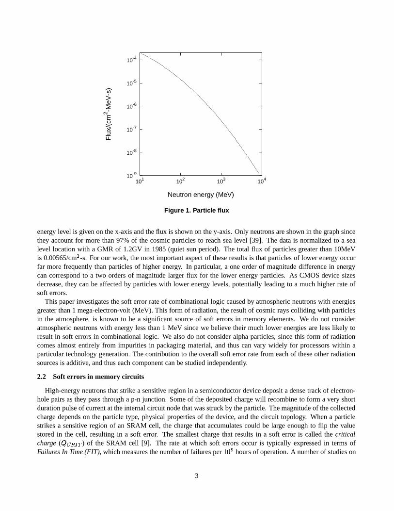
In the early 1980s, IBM conducted a series of experiments to measure the particle flux from cosmic rays [40].The graph in Figure 1 presents their findings. This graph shows the flux of neutrons by energy level, where the
2
10-4
10-5
10-6
10-7
10-8
10-9
101 102 103 104
Flu
x/(c
m2 -M
eV-s
)
Neutron energy (MeV)
Figure 1. Particle flux
energy level is given on the x-axis and the flux is shown on the y-axis. Only neutrons are shown in the graph sincethey account for more than 97% of the cosmic particles to reach sea level [39]. The data is normalized to a sealevel location with a GMR of 1.2GV in 1985 (quiet sun period). The total flux of particles greater than 10MeVis 0.00565/cm
�-s. For our work, the most important aspect of these results is that particles of lower energy occur
far more frequently than particles of higher energy. In particular, a one order of magnitude difference in energycan correspond to a two orders of magnitude larger flux for the lower energy particles. As CMOS device sizesdecrease, they can be affected by particles with lower energy levels, potentially leading to a much higher rate ofsoft errors.
This paper investigates the soft error rate of combinational logic caused by atmospheric neutrons with energiesgreater than 1 mega-electron-volt (MeV). This form of radiation, the result of cosmic rays colliding with particlesin the atmosphere, is known to be a significant source of soft errors in memory elements. We do not consideratmospheric neutrons with energy less than 1 MeV since we believe their much lower energies are less likely toresult in soft errors in combinational logic. We also do not consider alpha particles, since this form of radiationcomes almost entirely from impurities in packaging material, and thus can vary widely for processors within aparticular technology generation. The contribution to the overall soft error rate from each of these other radiationsources is additive, and thus each component can be studied independently.
2.2 Soft errors in memory circuits
High-energy neutrons that strike a sensitive region in a semiconductor device deposit a dense track of electron-hole pairs as they pass through a p-n junction. Some of the deposited charge will recombine to form a very shortduration pulse of current at the internal circuit node that was struck by the particle. The magnitude of the collectedcharge depends on the particle type, physical properties of the device, and the circuit topology. When a particlestrikes a sensitive region of an SRAM cell, the charge that accumulates could be large enough to flip the valuestored in the cell, resulting in a soft error. The smallest charge that results in a soft error is called the criticalcharge (
��������) of the SRAM cell [9]. The rate at which soft errors occur is typically expressed in terms of
Failures In Time (FIT), which measures the number of failures per ��� hours of operation. A number of studies on
3

soft errors in SRAMs have concluded that the SER for constant area SRAM arrays will increase as device sizesdecrease [19, 28, 29], though researchers differ on the rate of this increase.
A method for estimating SER in CMOS SRAM circuits was recently developed by Hazucha & Svensson [13].This model estimates SER due to atmospheric neutrons (neutrons with energies � 1MeV) for a range of submicronfeature sizes. It is based on a verified empirical model for the 600nm technology, which is then scaled to othertechnology generations. The basic form of this model is:
��������� �����exp
��� � ��������� � (1)
where �is a constant independent of device technology with the value ������� ���� � ,�is the neutron flux with energy � 1 MeV, in particles/(cm
�"!s),�
is the area of the circuit sensitive to particle strikes, in cm�,� ������
is the critical charge, in fC, and� �is the charge collection efficiency of the device, in fC
Two key parameters in this model are the critical charge (� ������
) of the SRAM cell and the charge collectionefficiency (
�#�) of the circuit.
� ������depends on characteristics of the circuit, particularly the supply voltage and
the effective capacitance of the drain nodes.� �
is a measure of the magnitude of charge generated by a particlestrike. These two parameters are essentially independent, but both decrease with decreasing feature size. FromEquation 1 we see that changes in the value of
� ������relative to
���will have a very large impact on the resulting
SER. The SER is also proportional to the area of the sensitive region of the device, and therefore it decreasesproportional to the square of the device size. Hazucha & Svensson used this model to evaluate the effect of devicescaling on the SER of memory circuits. They concluded that SER-per-chip of SRAM circuits should increase atmost linearly with decreasing feature size.
3 Soft Errors in Combinational Logic
A particle that strikes a p-n junction within a combinational logic circuit can alter the value produced by thecircuit. However, a transient change in the value of a logic circuit will not affect the results of a computation unlessit is captured in a memory circuit. Therefore, we define a soft error in combinational logic as a transient error inthe result of a logic circuit that is subsequently stored in a memory circuit of the processor.
A transient error in a logic circuit might not be captured in a memory circuit because it could be masked by oneof the following three phenomena:
Logical masking occurs when a particle strikes a portion of the combinational logic that is blocked fromaffecting the output due to a subsequent gate whose result is completely determined by its other input values.
Electrical masking occurs when the pulse resulting from a particle strike is attenuated by subsequent logicgates due to the electrical properties of the gates to the point that it does not affect the result of the circuit.
Latching-window masking occurs when the pulse resulting from a particle strike reaches a latch, but notat the clock transition where the latch captures its input value.
These masking effects have been found to result in a significantly lower rate of soft errors in combinationallogic compared to storage circuits in equivalent device technology [23]. However, these effects could diminishsignificantly as feature sizes decrease and the number of stages in the processor pipeline increases. Electrical
4

IN
CLK
OUT
CLK
D
Q’
Q D Q
Q’
Figure 2. Simple model of a pipeline stage
masking could be reduced by device scaling because smaller transistors are faster and therefore may have lessattenuation effect on a pulse. Also, deeper processor pipelines allow higher clock rates, meaning the latches in theprocessor will cycle more frequently, which may reduce latching-window masking.
The datapath of modern processors can be extremely complicated in nature, typically composed of 64 parallelbit lines and divided into 20 or more pipeline stages. We evaluate the effects of electrical and latching-windowmasking using the simple model for a processor pipeline stage illustrated in Figure 2. This model is just a one-widechain of homogeneous gates terminating in a level-sensitive latch. For the results presented in this paper we usestatic 3-input NAND gates with a fan-out of 4.
The number of gates in the chain is determined by the degree of pipelining in the microarchitecture, given asthe number of fan-out-of-4 inverter (FO4) gates that can be placed between two latches in a single pipeline stage.We use the FO4 metric because it allows us to characterize pipeline depth in a way that is largely independent ofdevice scaling [15]. During the last twelve years technology has scaled from 1000nm to 130nm and the amountof logic per pipeline stage has decreased from 84 to 12 FO4 contributing to a total of 60-fold increase in clockfrequency in the Intel family of processors, and aggressive pipelining could further reduce this to as few as 6 overthe next five to seven years [17]. For a given degree of pipelining, the number of gates in the pipeline stage is thelargest number that does not exceed the total delay of the corresponding FO4 chain.
CLKBAR
INPUT OUTPUT
CLK
Passgate
Figure 3. Circuit diagram of a pipeline latch
Figure 3 shows the circuit diagram of the latch we used in our simple pipeline model. The forward inverter isabout 6 times larger than the feedback inverter and the transistors are all of minimum length. We use level sensitivelatches in our pipeline model because they occupy less area than edge triggered flip-flops and so are more suitablefor superpipelining. They also allow for time borrowing techniques and offer less load to the clock distributionnetwork thus reducing the clock skew in the chip.
We used 3-input NAND gates with a fan-out of 4 because they are a common gate used in many logic designsand result in a conservative estimate of chip SER. The critical charge of a circuit increases with the capacitanceassociated with it. For example, the output node of a 3-input NAND gate has a much larger capacitance than aninverter with the same drive strength and so has a greater critical charge. By the same reasoning, a NAND gatewith a fan-out of 4 has a greater critical charge than a NAND gate that only drives a single following gate.
5

InducedCollection
Particle Charge
Voltage Pulseat Latch
InitialVoltage Pulse
1. Pulse Latching Model
2. Latching WindowMasking Model
CLK
ChargeElectrical Masking
Model
NO
1. Feature Size2. Logic Depth
Latched ?Error YES
Current Pulse
Voltage Pulse
Setup Logic Chain
Q
Q’
D Q
Q’
D
Figure 4. Process for determining the Soft Error Rate in a logic chain
4 Methodology
In most modern microprocessors, combinational logic and memory elements are constructed from the samebasic devices – NMOS and PMOS transistors. Therefore, we can use techniques for estimating the SER in memoryelements to assess soft errors in combinational logic. We will also use these techniques directly to compute the SERin memory elements for a range of device sizes, and compare the results to our estimates of SER for combinationallogic.
Our methodology for estimating the soft error rate in combinational logic considers the effects of CMOS devicescaling and the microarchitectural trend toward increasing depth of processor pipelines. We determine the softerror rate using analytical models for each stage of the pulse from its creation to the time it reaches the latch.Figure 4 shows the various stages the pulse passes through and the corresponding model used to determine theeffect on the pulse at that stage. In the first stage the charge generated by the particle strike produces a currentpulse, which is then converted into a voltage pulse after traveling through a gate in the logic chain. The electricalmasking model simulates the degradation of the pulse as it travels through the gates of the logic circuit. Finally amodel for the latching window determines the probability that the pulse is successfully latched. The remainder ofthis section describes each of these component models and how they are combined to obtain an estimate for theSER of combinational logic.
4.1 Device scaling model
We constructed a set of Spice Level 3 technology models corresponding to the technology generations from theSemiconductor Industry Association 1999 Technology Roadmap [33]. Values for drawn gate length ( ��� ������� ),supply voltage ( ��� ), and oxide thickness ( �� �� ) are taken directly from the roadmap. With the exceptionof threshold voltage ( �� ), the remaining parameters were obtained using a scaling methodology developed byMcFarland [25]. We chose a slightly different formula for computing the threshold voltage which scales betterto technologies with very low supply voltages. In the McFarland model, �� was set to � ��� � ������ �������� � ��� .The constant term of � ��� volts led to poor scaling for small values of ���� , so instead we use the formula �� �� ��� � ������ � ���� .
Table 1 presents the key characteristics of our CMOS device models.
4.2 Charge to voltage pulse model
When a particle strikes a sensitive region of a circuit element it produces a current pulse with a rapid rise time,but a more gradual fall time. The shape of the pulse can be approximated by a one-parameter function shown inEquation 2 [9].
"!$#&%(' �� *) #
� exp
� � #� � (2)
6

Technology Generation 600nm 350nm 250nm 180nm 130nm 100nm 70nm 50nm� � ������ (nm) 600 350 250 140 90 65 45 32"��� (V) 5.0 3.3 2.5 1.8 1.5 1.2 0.9 0.6� �� (nm) 11 7.6 4.0 2.5 1.9 1.5 1.2 0.8 �� (V) 1.0 0.735 0.596 0.466 0.407 0.344 0.277 0.205
Table 1. Key Characteristics of CMOS Device Models
�refers to the amount of charge collected due to the particle strike. The parameter � is the time constant,
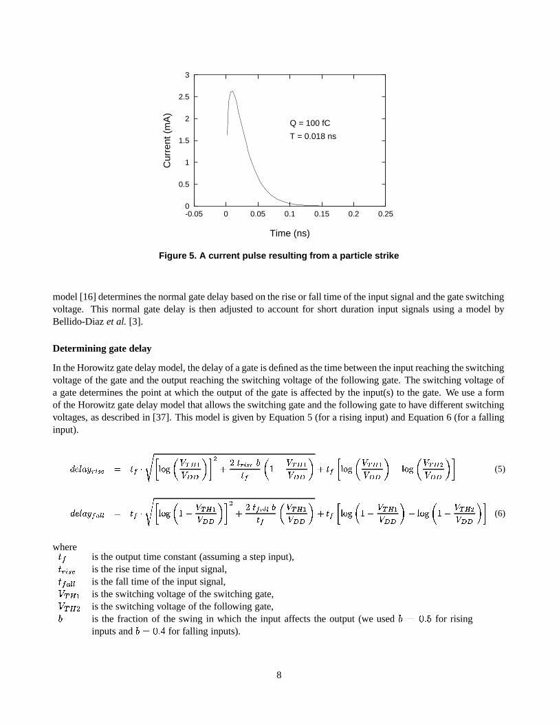
in units of nanoseconds, for the charge collection process and is a property of the CMOS process used for thedevice. If � is large it takes more time for the charge to recombine. If � is small, the charge recombines rapidly,generating a current pulse with a short duration. The rapid rise of the current pulse is captured in the square rootfunction and the gradual fall of the current pulse is produced by the negative exponential dependence. Figure 5illustrates the pulse waveform generated by this equation for the 100nm technology generation and a charge value� � �� � fC.
The time constant � scales approximately linearly with feature size in a log-log scale [12]. We constructed amodel for � for any CMOS technology, characterized by the minimum gate length � (in � m), by fitting a straightline through the values of � for 600nm, 350nm and 100nm from [13]. This model is given in Equations 3 and 4.
NMOS: � �exp
! � ����� ���� ! � % �� � % (3)
PMOS: � �exp
! � ��� ���� ! � % �� ��� % (4)
where � is specified in � m, and the resulting � value is in nanoseconds.The current pulse produced by a particle strike results in a voltage pulse at the output node of the device. We use
a Spice simulation to determine the rise time, fall time and effective duration of this voltage pulse. The effectiveduration is the elapsed time the pulse exceeds half the supply voltage. These three values are the final result of thisstage and become the input for the next phase, the electrical masking analytical model.
4.3 Electrical masking model
Electrical masking is the composition of two electrical effects that reduce the strength of a pulse as it passesthrough a logic gate. Circuit delays caused by the switching time of the transistors cause the rise and fall time ofthe pulse to increase, reducing its effective duration. For short duration pulses, pulse duration is further reducedbecause the gate may start to turn off before the output reaches its full amplitude. As pulse duration decreases,this second effect becomes greater, and thus these effects cascade from one gate to the next, and can eventuallydegrade the pulse to the extent that it cannot affect the result latch.
We define the rise time of a pulse to be the time for the pulse to rise from ����� to ���� . For pulses that donot actually rise all the way to ���� , we extend the rising edge and measure rise time to the point where this edgecrosses ��� . Fall time is defined similarly. Using these definitions, rise time and fall time are best thought of asdescribing the slope of the rising and falling edge. For the experiments reported in this paper, we model a pipelinestage as a chain of static, 3-input, fan-out-of-4 NAND gates. One output of each gate feeds one input of the nextgate in the chain, with the other inputs fixed at a logical 1. In this model, each gate in the chain inverts the signal onits one non-fixed input, so a rising pulse entering the gate becomes a falling pulse leaving the gate, and vice-versa.
We constructed a model for electrical masking based on the propagation delay of an electrical signal througha logic gate. Gate delay is determined using a composition of two existing models. The Horowitz gate delay
7
0
0.5
1
1.5
2
2.5
3
-0.05 0 0.05 0.1 0.15 0.2 0.25
Cur
rent
(m
A)
Time (ns)
Q = 100 fC
T = 0.018 ns
Figure 5. A current pulse resulting from a particle strike
model [16] determines the normal gate delay based on the rise or fall time of the input signal and the gate switchingvoltage. This normal gate delay is then adjusted to account for short duration input signals using a model byBellido-Diaz et al. [3].
Determining gate delay
In the Horowitz gate delay model, the delay of a gate is defined as the time between the input reaching the switchingvoltage of the gate and the output reaching the switching voltage of the following gate. The switching voltage ofa gate determines the point at which the output of the gate is affected by the input(s) to the gate. We use a formof the Horowitz gate delay model that allows the switching gate and the following gate to have different switchingvoltages, as described in [37]. This model is given by Equation 5 (for a rising input) and Equation 6 (for a fallinginput).
�������������� �� ����� � ��������� �"!$#&%�(')'+*-,/. 021 � ���� -3� � �54-67�"!$#&%�(')'8*90 ��� ���������:�;!(#<%�(')'8* 6=�����>�:�"!$# .�;')'+*<,(5)
�?�����?� �A@CBDB � � � � � ���������E4-6F�;!(#<%� ')'+*-,/. 0G1 � �A@CBHB$3��� �:�;!$#&%� ')'+*+0 � � ���I�����54-67�"!$#&%� ')'+* 6J�I�����54-67�"!$# .� ')'8*<,(6)
where#CKis the output time constant (assuming a step input),#MLMNPORQis the rise time of the input signal,#CK�SUTVTis the fall time of the input signal, ��XW is the switching voltage of the switching gate, �� � is the switching voltage of the following gate,Yis the fraction of the swing in which the input affects the output (we used
Y � � � for risinginputs and
Y � � ��� for falling inputs).
8

TH
DD /2
DD
t0 t1 t2
0
t3
limit
p
t4 t5
GNDGate Output
Gate Input
V
V
V
T
Tt
T
Figure 6. The Delay Degradation Effect
The gate switching voltages are determined using an iterative bisection method. This procedure adjusts theswitching voltages until the rise and fall times predicted by the model are within 15% of values obtained fromSpice simulations. Table 2 shows the switching voltages determined using this procedure for the NAND gate usedin the experiments. To calculate the delay for a rising edge, we set �� W to L NPO�Q and �� � to K SUTHT ; for a fallinginput, �� W is set to K�SATHT and �� � to L N ORQ .
Technology Generation 600nm 350nm 250nm 180nm 130nm 100nm 70nm 50nm L NPO�Q � "��� 0.16 0.50 0.38 0.31 0.31 0.38 0.38 0.38 K�SATHT � ��� 0.25 0.25 0.25 0.25 0.25 0.25 0.25 0.25
Table 2. Switching Voltage of the gates
The pulse generated by a particle strike typically has a short duration. Thus, when a pulse passes through a logicgate, the output of the gate might not have time to fully switch in response to the pulse before it disappears fromthe gate input. If the output has not fully switched, the gate can respond to the new state of its inputs more quickly,and thus the gate delay is reduced. This effect is know as the delay degradation effect [3]. In this situation, thevalue generated at the gate output begins switching in the opposite direction before reaching the peak amplitudeof the input, which results in an output signal with reduced amplitude. We use a model by Bellido-Diaz et al. tosimulate this effect on an error pulse as it passes through a logic gate.
Figure 6 illustrates the delay degradation effect. At time# � , the gate input crosses the gate switching voltage, �� , and the gate output starts to rise. At time
# Wthe gate output crosses ��� � � , and thus has logically transitioned
to the new output value. Then the gate input begins rising and crosses back above the gate switching voltage attime
# � , and as a result, the gate output begins to fall before it could rise completely to ��� . Since the outputdid not reach it’s full amplitude, it requires less time to fall back below ���� � � , resulting in a smaller than normalpropagation delay
#��. If the input had remained low until time
#��, the output would rise fully to ���� , and a
subsequent input transition will result in a normal propagation delay.The Bellido-Diaz delay degradation model is given in Equation 7.
9

b c
d e
aDD Input Pulse
Output Pulserise
rise
fall
TH2
TH1
V
V
V
GND
t
delay
t
Figure 7. Model to compute rise/fall time based on gate delay
# � � # � � � ���������� � where � � � T N�� N��� (7)
# � � is the normal propagation delay with zero degradation effect, which we determine using the Horowitz model.The rest of the equation captures the degradation effect. The time between the output transition and the next inputtransition is ( � - � � ), and � is a parameter proportional to the time needed for the gate to fully switch, � T N�� N�� .Determining output pulse characteristics from gate delay
We approximate the input and output of the gate as piecewise-linear signals, and use a simple linear model todetermine the rise and fall time of the gate output based on rise and fall time of the input and the gate delay.Figure 7 illustrates the model for the fall time of the gate output. In this figure, the rising edge of the pulse ispassing through a gate, causing the output to fall from ��� to � � � . The rise time for this rising edge is
# L NPO�Q.
When the input pulse crosses �� W , the switching voltage of the gate, the output begins to fall. The output reachesthe �� � , the switching voltage of the following gate, after time � ������� L NPO�Q , the gate delay for the rising edge ofthe pulse. Thus we can determine the base and height of triangle
� Y��. The fall time of the output pulse,
#�K�SUTVT, is
the base of the equivalent triangle
� � � , whose height is simply ��� . Thus, we calculate# K SUTHT
as follows:
#CK�SUTVT � � ������� L NPO�Q�� �� �� �"��� � (8)
We assume that the input to the gate is stable when the pulse arrives, and thus there is no delay degradation forthe leading edge (which could be either a rising or falling edge). However, when the pulse is short, the gate delayfor trailing edge could be significantly smaller than that of the leading edge, and this reduces the duration of theoutput pulse. Thus, we determine the duration of the output pulse as
�! #" � #%$'&(*),+�� ��+�� � �! �" � #,$-&.( N�/ ��+�� � ! � ������� T Q S�0 N�/21 � � ������� � L S N T N�/21 % (9)
10

4.4 Pulse latching model
Recall that our definition of a soft error in combinational logic requires an error pulse to be captured in amemory circuit. Therefore, in our model a soft error occurs when the error pulse is stored into the level-sensitivelatch at the end of a logic chain. We only consider a value to be stored in the latch if it is present and stable whenthe latch closes, since this value is passed to the next pipeline stage.
When a voltage pulse reaches the input of a latch, we use a Spice simulation to determine if it has sufficientamplitude and duration to be captured by the latch. The simulation is done in two steps. First we determine thepulse start time, the shortest time between the rising edge of the pulse and clock edge for which the pulse could belatched. This is similar to a setup time analysis for the latch, except that the input data waveform has the slope ofthe pulse at the latch input. The second step is to determine the minimum duration pulse (measured at the thresholdvoltage) that could be latched. For this step, we position the rising edge of the pulse at the point determined in thefirst step, and then vary the duration until the minimum value is determined. We studied the nature of the pulsestart time and minimum duration using separate experiments and found that the pulse start time can be modeledby a linear function of the rise time of the pulse, and the minimum duration can be modeled by a linear function ofthe rise time and fall time. For example, the pulse start time (in ps) of our pipeline latch in our 600nm technologycan be computed as follows:
start��� ��� � � ����� # L NPO�Q
and the minimum duration (in ps) is given by
duration� �� � � � ��� � � #ML NPO�Q � � ��� � � #CK�SATHT
In our method for computing SER for combinational circuits, the start time and minimum duration of an errorpulse must be determined on a very frequent basis. Therefore, it is important that we determine these values usinga simple model rather than with Spice simulations so that run times for the overall model are reasonable. Thepulse start time and minimum duration given by these models correlate very highly with the pulse start time andminimum duration determined from Spice simulations, and therefore allow us to replace an expensive simulationrun with a very inexpensive calculation without significant loss in accuracy.
Given the rise and fall time of a pulse at the latch input, the simulation determines the minimum duration(measured at the threshold voltage) required for the pulse to be latched. If the duration of the pulse at the latchinput exceeds this minimum duration, the pulse has the potential to cause a soft error. This method determinesif a particle-induced pulse in an otherwise stable, correct input signal is strong enough to be latched. It is alsopossible that a particle-induced pulse could delay the correct input signal from arriving at the latch input in timeto be latched, thus causing an error. This type of error is referred to as a delay fault. Due to the complexityof modeling these faults, we have chosen to exclude them from our study. Bernstein found that delay faults arenegligible in current technologies due to the common design practice of incorporating a 5%-10% safety margininto the clock cycle [4]. However, such faults could become much more common as clock frequency increasesand safety margins are squeezed to increase performance.
4.5 Latching-window masking model
A latch is only vulnerable to a soft error during a small window around its closing clock edge. The size of thislatching window is simply the minimum duration pulse that can be latched, which depends on the pulse rise andfall time. A pulse that is present at the latch input throughout the entire latching window will be latched and causesa soft error. Any pulse with a duration smaller than the duration of the latching window cannot cause a soft error.
11
Clock Cycle
Clock
Latching Window
Soft error
Masked pulses
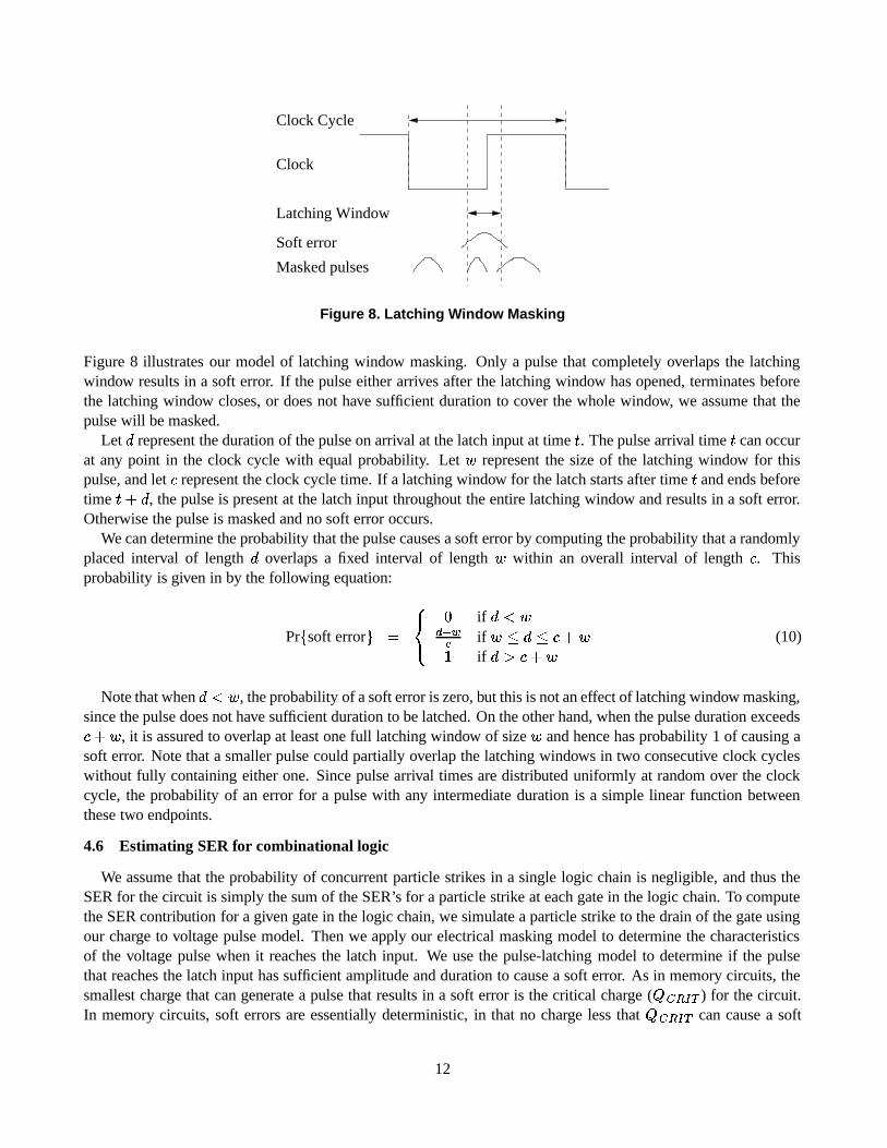
Figure 8. Latching Window Masking
Figure 8 illustrates our model of latching window masking. Only a pulse that completely overlaps the latchingwindow results in a soft error. If the pulse either arrives after the latching window has opened, terminates beforethe latching window closes, or does not have sufficient duration to cover the whole window, we assume that thepulse will be masked.
Let � represent the duration of the pulse on arrival at the latch input at time#. The pulse arrival time
#can occur
at any point in the clock cycle with equal probability. Let � represent the size of the latching window for thispulse, and let
�represent the clock cycle time. If a latching window for the latch starts after time
#and ends before
time# � � , the pulse is present at the latch input throughout the entire latching window and results in a soft error.
Otherwise the pulse is masked and no soft error occurs.We can determine the probability that the pulse causes a soft error by computing the probability that a randomly
placed interval of length � overlaps a fixed interval of length � within an overall interval of length�. This
probability is given in by the following equation:
Pr�soft error � � ���� � if ����0 ��� if �� �� � � �
if � � � � � (10)
Note that when ���� , the probability of a soft error is zero, but this is not an effect of latching window masking,since the pulse does not have sufficient duration to be latched. On the other hand, when the pulse duration exceeds� � � , it is assured to overlap at least one full latching window of size � and hence has probability 1 of causing asoft error. Note that a smaller pulse could partially overlap the latching windows in two consecutive clock cycleswithout fully containing either one. Since pulse arrival times are distributed uniformly at random over the clockcycle, the probability of an error for a pulse with any intermediate duration is a simple linear function betweenthese two endpoints.
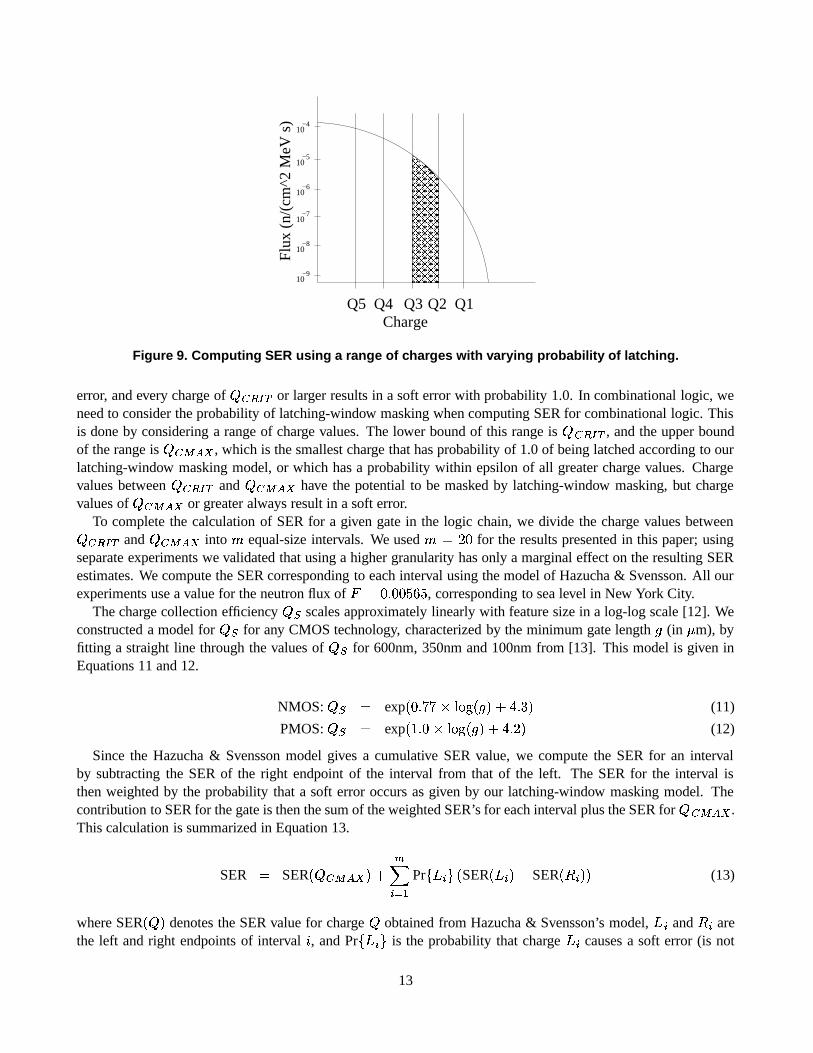
4.6 Estimating SER for combinational logic
We assume that the probability of concurrent particle strikes in a single logic chain is negligible, and thus theSER for the circuit is simply the sum of the SER’s for a particle strike at each gate in the logic chain. To computethe SER contribution for a given gate in the logic chain, we simulate a particle strike to the drain of the gate usingour charge to voltage pulse model. Then we apply our electrical masking model to determine the characteristicsof the voltage pulse when it reaches the latch input. We use the pulse-latching model to determine if the pulsethat reaches the latch input has sufficient amplitude and duration to cause a soft error. As in memory circuits, thesmallest charge that can generate a pulse that results in a soft error is the critical charge (
� ������) for the circuit.
In memory circuits, soft errors are essentially deterministic, in that no charge less that� ��� � �
can cause a soft
12
������������������������������������������
��������������������������������������������������������������������������������������������������
��������������������������������������������������������������������������������������������������
−910
−810
−710
−610
−510
−410
Q5 Q4 Q3 Q2 Q1Charge
Flux
(n/
(cm
^2 M
eV s
)
Figure 9. Computing SER using a range of charges with varying probability of latching.
error, and every charge of� ��� ��
or larger results in a soft error with probability 1.0. In combinational logic, weneed to consider the probability of latching-window masking when computing SER for combinational logic. Thisis done by considering a range of charge values. The lower bound of this range is
� ��� � �, and the upper bound
of the range is� ��� ���
, which is the smallest charge that has probability of 1.0 of being latched according to ourlatching-window masking model, or which has a probability within epsilon of all greater charge values. Chargevalues between
� ��� � �and
����� ��have the potential to be masked by latching-window masking, but charge
values of� ��� ���
or greater always result in a soft error.To complete the calculation of SER for a given gate in the logic chain, we divide the charge values between� ������
and� ��� ��
into equal-size intervals. We used � � � for the results presented in this paper; usingseparate experiments we validated that using a higher granularity has only a marginal effect on the resulting SERestimates. We compute the SER corresponding to each interval using the model of Hazucha & Svensson. All ourexperiments use a value for the neutron flux of
� � � � � � � , corresponding to sea level in New York City.The charge collection efficiency
� �scales approximately linearly with feature size in a log-log scale [12]. We
constructed a model for�#�
for any CMOS technology, characterized by the minimum gate length � (in � m), byfitting a straight line through the values of
� �for 600nm, 350nm and 100nm from [13]. This model is given in
Equations 11 and 12.
NMOS:��� �
exp! � � ��� ���� ! � % � � ��� % (11)
PMOS:��� �
exp! � � ���� ! � % � � ��� % (12)
Since the Hazucha & Svensson model gives a cumulative SER value, we compute the SER for an intervalby subtracting the SER of the right endpoint of the interval from that of the left. The SER for the interval isthen weighted by the probability that a soft error occurs as given by our latching-window masking model. Thecontribution to SER for the gate is then the sum of the weighted SER’s for each interval plus the SER for
� ��� ��.
This calculation is summarized in Equation 13.
SER�
SER! � ��� �� % �
�� N � W Pr
� � N � ! SER! � N % � SER
! � N %�%(13)
where SER! � %
denotes the SER value for charge�
obtained from Hazucha & Svensson’s model, � N and� N
arethe left and right endpoints of interval
$, and Pr
� � N � is the probability that charge � N causes a soft error (is not
13

1e-12
1e-11
1e-10
1e-09
1e-08
1e-07
1e-06
1e-05
1e-04
1e-03
1e-02
600nm 1992
350nm 1994
250nm 1997
180nm 1999
130nm 2002
100nm 2005
70nm 2008
50nm 2011
Sof
t Err
or R
ate
(FIT
/[bit|
latc
h|lo
gic]
)
Technology Generation
H&S SRAMSRAM
latchlogic, 6 FO4slogic, 8 FO4slogic, 12 FO4slogic, 16 FO4s
Figure 10. SER of individual circuits
latching-window masked). This computation is illustrated in Figure 9. The contribution of the shaded region tooverall SER is the SER for charges greater than
���minus the SER for charges larger than
� � , multiplied by thesoft error probability associated with charge
���.
5 Results
5.1 Circuit Soft Error Rate
The circuits of a modern microprocessor fall into three basic classes: SRAM cells, latches, and combinationallogic. We estimated the SER for an individual SRAM cell, latch, and logic chain using the methodology describedin Section 4. Figure 10 shows the predicted SER by technology generation and pipeline depth. The x-axis plotsthe CMOS technology generation, arranged by actual or expected date of adoption. The y-axis plots the SER fora single SRAM cell, latch or logic chain, in Failures In Time (FIT) – the number of failures per �� hours ofoperation – on a log scale. Also shown in this graph are the results reported by Hazucha and Svensson for SRAMSER, using their scalable SER model [13].
The SER of a single SRAM cell declines gradually with decreasing feature size. There are three basic factorsthat combine to produce this trend. The drain area of each transistor, which is the region sensitive to particle strikes,decreases quadratically as feature size decreases. Critical charge also decreases significantly with decreasingfeature size, primarily due to lower supply voltage levels, but also due to reduced capacitance in the smaller circuitnodes. Finally, charge accumulation in the transistor decreases due to reduced voltages and smaller node volume.In SRAM cells, the decrease in critical charge is effectively offset by reduced charge accumulation, and thus thedecrease in sensitive area leads to a decrease in circuit SER. Our results show good correlation with those ofHazucha and Svensson; both results show the same basic trend, and the absolute error is less than one order ofmagnitude for all technologies, which can be attributed to differences in CMOS parameters.
The SER of a single latch stays relatively constant as feature size decreases. For latches, the effect of thedecreasing area of the sensitive region is offset by the decrease in critical charge, as explained below. In contrast,the SER for a single logic chain changes dramatically as feature size decreases – increasing over six orders of
14

1e-01
1e+00
1e+01
1e+02
1e+03
1e+04
600nm 1992
350nm 1994
250nm 1997
180nm 1999
130nm 2002
100nm 2005
70nm 2008
50nm 2011
Qcr
it (f
C)
Technology Generation
logic, 16 FO4slogic, 4 FO4slogic, 0 FO4
latchSRAM
QS
Figure 11. Critical charge for a single SRAM cell/latch/logic chain
600nm 350nm 250nm 180nm 130nm 100nm 70nm 50nmlogic, 16 FO4s N/A 676 489 250 116 61.3 24.0 10.4logic, 4 FO4s 4160 509 336 131 63.9 35.2 16.0 7.02logic, 0 FO4s 1130 386 265 99.3 48.8 27.3 13.2 5.57latches 360 120 82.4 31.9 15.0 7.96 3.73 1.66SRAM 146 48.8 33.7 12.9 6.31 3.43 1.52 0.670QS 52.3 34.6 26.8 17.2 12.2 9.53 7.19 5.54
Table 3. Critical charge for an SRAM cell/latch/logic chain by feature size and pipeline depth
magnitude from 600nm to 50nm. In logic circuits, the electrical effect of decreasing critical charge far outweighsthe effect of decreasing area of the sensitive region. The effect of superpipeling is illustrated by the larger SER forlogic circuits at higher pipeline depths (smaller clock period in FO4 delays) within each technology generation.
Decreasing critical charge: Recall that the empirical model for SER (Equation 1) has an exponential depen-dence on the ratio
� � ��� �� � ���. When this ratio is large, this factor dominates the SER expression, but its
influence decreases rapidly as the value of� ������
approaches�#�
. Figure 11 plots� ������
, in femto-Coulombs,for an individual SRAM cell, latch, and logic circuit, along with
� �, the charge collection efficiency, by technol-
ogy generation. For combinational logic, the graph shows� ������
values for a particle strike 0, 4, and 16 FO4gate-delays from the latch. Note that the y-axis of the graph is log-scale. This data is also presented in Table 3. Thevalues shown are for NMOS devices, but are essentially equivalent to PMOS devices. Note: The data presentedin Figure 11 differs somewhat from that contained in our earlier conference paper [34]. This is due to a minorproblem in our technique for determining
� � L N�� which overstated� � L N�� values whenever
� � L N�� was less than���
.Fortunately, this error has virtually no significant impact on the results shown in the remainder of the paper.
For a single SRAM cell,� ������
is only slightly larger than� �
in the 350nm and 250nm technology genera-tions, and falls below
� �at 180nm. Even though
� ������continues to fall as feature size decreases, the effect on
15

0
10
20
30
40
50
60
70
80
600nm 1992
350nm 1994
250nm 1997
180nm 1999
130nm 2002
100nm 2005
70nm 2008
50nm 2011
Qcr
it/Q
s
Technology Generation
logic, 16 FO4slogic, 4 FO4slogic, 0 FO4
latchSRAM
Figure 12. Ratio of critical charge to charge collection efficiency for SRAM/latch/logic
SER is relatively small in comparison to the decreasing area of the sensitive region.For a single pipeline latch,
� ��� � �is nearly an order of magnitude larger than
� �in the 600nm technology
generation, but declines steadily as feature size decreases, and should fall below� �
by the 100nm technologygeneration. As
��������decreases relative to
�#�, the electrical effects of decreasing feature size diminish, and SER
is more heavily influenced by the area of the sensitive region.For a single logic chain,
� ������decreases in a similar fashion to that of memory circuits, but at all points
is much larger in absolute terms. Logic transistors are typically wider than transistors used in memory circuits,where density is important, and therefore are less sensitive to small charge values. Thus, the electrical effect ofdecreasing
��������is much larger than the area effect in all technology generations. Figure 11 also illustrates the
effect of electrical masking on the SER of logic circuits. For all feature sizes below 600nm, the� ������
for 16FO4 logic gates is consistently about twice that of the 0 FO4 circuit, and this difference is the result of degradationof the error pulse as it passes through the 16 FO4 gates. Contrary to our expectations, our results do not show anyreduction in this effect with decreasing feature size. We conclude that the primary effect of electrical masking isto screen out marginal pulses; the degradation effect on pulses with sufficient strength to be latched is minimal.
The effect of the declining� ������ � � �
ratio can be directly observed in Figure 12, which plots this ratio for asingle SRAM cell, pipeline latch, and logic chain by technology generation. This graph shows that
� ��� �� � ���of SRAMs is relatively small for all feature sizes, confirming that reductions in
� ��� � �due to device scaling will
have only a secondary effect on SER for SRAM circuits. The� ��� � � � � �
ratio for latches is significantly largerthan SRAMs in the 600nm technology, but decreases to nearly the same level as SRAMs by the 180nm technologygeneration. Device scaling in memory elements affects the critical charge and charge collection efficiency almostequally because smaller transistors are more sensitive to a particle strike but have very little sensitive volume forcharge collection. Logic shows the largest decrease in the
� ��� � � � � �ratio, but remains above the level of SRAM
cells and latches even in the 50nm technology generation.
Effects on latching-window masking: We also performed experiments to determine the effects of technologytrends on latching-window masking. We recomputed the SER of combinational logic with the assumption that
16

0
50
100
150
200
250
300
600nm 1992
350nm 1994
250nm 1997
180nm 1999
130nm 2002
100nm 2005
70nm 2008
50nm 2011
SE
R (
nolw
m)/
SE
R (
lwm
)
Technology Generation
16 FO4s12 FO4s 8 FO4s 6 FO4s
Figure 13. Effect of latching-window masking
any charge larger than� ��� ��
will result in a soft error. Then we divided by the original SER value to obtain aratio that indicates the effect of latching window masking for a given technology generation and pipeline depth.Figure 13 presents the results of this analysis. From the graph we can see that for each technology generationthe latching-window masking effect decreases with decreasing number of gates between latches. This is becauseat lower clock rates the latching window occupies a smaller fraction of the clock period. For a given pipelinedepth, latching-window masking is only a function of the relative widths of the latching window and the errorpulse at the latch. As feature size decreases, latches have much shorter response times and so have smallerlatching windows. This increases the probability that a pulse of a given duration will overlap the window (seeEquation 10), and hence reducing the effect of latching-window masking. Figure 13 confirms this trend, witha general decline in the effect of latching-window masking for all pipeline depths. (The results for the 600nmtechnology generation are conspicuously contrary to the expected trend. We believe this is due to anomalies withour method for recomputing the SER without latching-window masking effects, but we were unable to completelyconfirm this.) In summary, our results demonstrate that latching window masking is reduced by both higherdegrees of pipelining and reduction in feature size.
5.2 Processor Soft Error Rate
Now we determine how soft errors in SRAM cells, latches, and logic circuits contribute to the SER of the entireprocessor chip for future microprocessor technologies. As feature sizes decrease, the number of transistors thatcan be placed on a fixed size die increases quadratically, creating significantly greater opportunity for soft errors.Since the rate of soft errors is different in SRAM cells, latches and logic, the SER of the processor will dependon the chip area devoted to each type of device. To estimate the SER of the entire chip we have developed achip model that describes the transistor decomposition into logic, SRAMs and latches. From the chip model wedetermine the total number of SRAM bits, latches and logic chains and then scale the per unit SER of each circuitby their number on the chip to obtain the SER/chip.
17

Device size Total SRAM Latches Logic gates600nm 5.17 M 4.07 M (78.8%) 0.06 M ( 1.2%) 1.03 M (20.0%)350nm 15.2 M 11.9 M (78.8%) 0.19 M ( 1.2%) 3.04 M (20.0%)250nm 29.7 M 23.4 M (78.8%) 0.37 M ( 1.3%) 5.95 M (20.0%)180nm 95.0 M 74.8 M (78.8%) 1.18 M ( 1.2%) 19.0 M (20.0%)130nm 229 M 181 M (78.8%) 2.87 M ( 1.3%) 45.9 M (20.0%)100nm 440 M 347 M (78.8%) 5.50 M ( 1.2%) 88.1 M (20.0%)70nm 919 M 724 M (78.8%) 11.4 M ( 1.3%) 183 M (20.0%)50nm 1818 M 1431 M (78.8%) 22.7 M ( 1.3%) 363 M (20.0%)
Table 4. Transistors per chip for 16 FO4 pipeline using quadratic scaling assumption
Pipeline depth SRAM bits Latches Logic gates16 FO4s 1995 K (78.8%) 32 K ( 1.2%) 507 K (20.0%)12 FO4s 1984 K (78.3%) 42 K ( 1.7%) 507 K (20.0%)8 FO4s 1963 K (77.5%) 63 K ( 2.5%) 507 K (20.0%)6 FO4s 1942 K (76.7%) 84 K ( 3.3%) 507 K (20.0%)
Table 5. Chip Model for 350nm device size
Chip Model: We used the Alpha 21264 microprocessor as the basis for constructing our chip model. The Alpha21264 was designed for a 350nm process and has 15.2 million transistors on the die [22]. Based on a detailedarea analysis of die photos of the Alpha 21264 [21], we concluded that approximately 20% of transistors are inlogic circuits and the remaining 80% are in storage elements in the form of latches, caches, branch predictors, andother memory structures. Our chip model applies this basic allocation to all feature sizes. The total number oftransistors per chip is scaled quadratically from the baseline Alpha 21264 based on feature size. Table 4 presentsthe total number of transistors per chip, and the transistors devoted to each circuit class for each technology basedon this assumption.
A typical SRAM bit requires 6 transistors, the level sensitive latch we use in our model consists of 6 transistors,and we assume each logic gate also uses 6 transistors. These assumptions are quite realistic and using slightlydifferent values for these numbers will not affect the overall trend noticeably.
The allocation of memory element transistors to SRAM cells and latches depends on the number of latchesrequired by the processor pipeline, which depends on pipeline depth. We allocate one latch for each logic chain,and the remaining memory element transistors are allocated to SRAM cells. Table 5 illustrates how our modelallocates transistors to SRAM bits, latches, and logic gates in the 350nm feature size for four pipeline depths. Ourchip model is summarized in the following equations:
total transistors�
15.2 million �
350nmfeature size
� �logic chains
� logic transistorsgates per logic chain
transistors per gate
latches�
logic chains
SRAM bits� !�!
total transistors ��� � % � !
latches � %�% � �
Results: Using the SER of individual elements shown in the previous section and our chip model, we computedthe SER/chip for each class of components for each technology generation and pipeline depth of our study. The
18

1e-08
1e-06
1e-04
1e-02
1e+00
1e+02
1e+04
600nm 1992
350nm 1994
250nm 1997
180nm 1999
130nm 2002
100nm 2005
70nm 2008
50nm 2011
Sof
t Err
or R
ate
(FIT
/chi
p)
Technology Generation
SRAMlatch, 6 FO4slatch, 8 FO4slatch, 12 FO4slatch, 16 FO4slogic, 6 FO4slogic, 8 FO4slogic, 12 FO4slogic, 16 FO4s
Figure 14. SER/chip for SRAM/latches/logic
results are presented in Figure 14. As discussed above, SER/chip of SRAM shows little increase as feature sizedecreases. To simplify the graph we only plot SRAM data for one pipeline depth. Pipeline depth has no noticeableeffect on the SRAM SER/chip, since the percentage of chip area allocated to SRAM changes very little. SER/chipin latches increases only slightly for all pipeline depths, a combined effect of the relatively constant SER/latch andthe increasing number of latches at smaller feature sizes. SER/chip of latches increases for deeper pipelines, duesolely to the greater number of latches required for deeper pipeline microarchitectures.
SER/chip in combinational logic increases dramatically from 600nm to 50nm, from 10 � � to approximately 10�,
or nine orders of magnitude. This is simply the composition of a 10 � increase in SER per individual logic chainand more than 100 times increase in logic chains per chip. At 50nm with 6 FO4 pipeline, the SER per chip oflogic exceeds that of latches, and is within two orders of magnitude of the SER per chip of unprotected memoryelements. Mainstream microprocessors from Intel [18] and other vendors [21] have employed ECC to reduce SERof SRAM caches at feature sizes of up to 350nm. For processors that use ECC to protect a large portion of thememory elements on the chip, logic will quickly become the dominant source of soft errors.
6 Discussion
The primary focus of our study has been to establish the basic trend in SER of combinational logic and themajor influences on this trend. Our model considers the effects of device scaling and superpipelining trends, andthe corresponding effects on electrical and latching window masking. This section discusses other factors may alsohave some influence on SER of combinational logic, but are not considered in our model to simplify the modelconstruction and analysis.
Circuit Implementations: We restricted our analysis to static combinational logic circuits and level-sensitivelatches. Modern microprocessors frequently employ a diverse set of circuit styles, including dynamic logic, andlatched domino logic, and a variety of latches, including edge-triggered flip flops, with different combinations ofperformance, power, area, and noise margin characteristics. We believe our model could be extended to includethese additional circuit styles and latch designs.
19

A B C
A
B
C
OUT
2W 2W 2W
3W
3W
3W
3
1
2
Figure 15. Static 3-input NAND gate
n−logic
block
clk
Inputs
Output
Figure 16. CMOS domino logic : latched version
Figure 15 illustrates the static 3-input NAND gate used in our model. The transistors are sized so that the worstcase rise/fall time of the gate is equal to an inverter with NMOS width ’W’ and PMOS width ’2W’ which makesits drain area larger than that of the equivalent inverter. In this gate there are 3 nodes where a particle can strikeand have an effect on the output, but due to capacitive charge sharing only a direct hit to the output node has asignificant contribution to soft error rate.
The use of dynamic logic could substantially increase the SER, since each gate has built-in state that canreinforce an error pulse as it travels through a logic chain. Figure 16 shows a NAND gate implemented in latchedCMOS domino logic. Note that the cell contains a feedback inverter whose purpose is to hold the value of theoutput constant. Typically this inverter is designed with a low switching voltage to reduce delay through the circuit,lowering its noise margin and making it more susceptible to soft errors.
We use level sensitive latches in our pipeline model because they occupy less area than edge triggered flip-flopsand so are more suitable for superpipelining. They also allow for time borrowing techniques and offer less load tothe clock distribution network thus reducing the clock skew in the chip. However, the critical charge for this typeof latch is typically smaller than that of a static edge-triggered latch. If we had used an edge-triggered, we expectthat the estimated SER for both latches and logic would be reduced.
For superpipelined microarchitectures, latches should be designed to be very fast and occupy minimal area. Acommon technique for increasing latch speed is to increase the widths of the latch transistors, but this increasesthe area of the sensitive regions in the latch, thus increasing the potential for soft errors. One approach to reducinglatch area is to eliminate the passgate typically placed within the feedback loop of the latch. This also increasesthe positive feedback in the loop which makes the latch faster and more capable of latching weak input pulses, butincreases the likelihood of latching an error pulse caused by a particle strike. These points illustrate the importanceof design choices on the overall SER.
Logical Masking: Logical masking is another masking effect that inhibits soft errors in combinational logic andcould have a significant effect on the SER. Since our model places every logic gate on an active path to a latch,we do not account for the the effect of logical masking. Incorporating logical masking would probably increasethe complexity of the model significantly, since the model would need to consider actual circuits and associatedinputs. Massengill et al. developed a specialized VHDL simulator that could analyze soft faults in an actual circuitand model the effects of logical masking [24]. They found that effect of logical masking on SER depends heavilyon circuit inputs.
Effects similar to logical masking can also occur in memory elements. For example, if a soft error occurs ina memory element that holds dead data – data that will not be used again – it is in some sense logically masked.
20

Another example is a soft error in a memory structure such as a branch predictor, which may lead to reducedperformance but not produce incorrect results. Due to the difficulty in modeling these effects, we have chosen toexclude all forms of logical masking in memory elements or logic from our model.
Finally, it is difficult to predict the overall effect of technology trends on logical masking. Device scalingprovides more transistors on the processor die which may encourage more speculative processing, which couldincrease the potential for logical masking. Deeper pipelines will reduce the number gates between pipeline latches,which decreases the opportunity for a pulse to be logically masked before arriving at a latch and causing a softerror. While such effects could be significant, we feel it is unlikely that they would alter the basic SER trendspredicted by our model.
Alpha Particles: Our study only considers soft errors resulting from high-energy neutrons. Another importantsource of soft errors in microprocessors is alpha particles that originate from radioactive decay of uranium orthorium impurities in chip and packaging materials. In sub-0.25um technologies with decreasing supply voltageand node capacitances, the SER due to alpha particles presents a major reliability concern to logic processesbecause of the quadratically decreasing critical charge [7, 8]. Packaging alternatives such as lid coat or flip chipstrongly influence the soft error rate induced by alpha particles. Alpha particle SER increases more rapidly withdecreasing critical charge than neutron induced SER [35, 36]. For circuits with
� ������in the range of 10-40 fC, the
alpha particle SER becomes comparable to that of neutron SER [11]. In our experiments, this range correspondsto SRAM cells and latches in 180nm and later technologies and logic circuits in 50nm and later technologies. Ourmodel could be adapted to estimate the SER due to alpha particle radiation. This would require a technology-scaled alpha particle model for the charge collection efficiency and the time constant for the NMOS and PMOStransistors. A key input to this model would be the expected flux of alpha particles, which is determined mainlyby package design.
Fabrication Technology: The process used to manufacture a semiconductor device has a significant effect onthe SER of the device. New process technologies such as silicon-on-insulator (SOI) have been shown to sig-nificantly reduce SER. The SOI process embeds an oxide (insulator) layer in the substrate which significantlydecreases the volume available for charge collection. This reduces the amount of charge collected due to a particlestrike, which decreases the probability of soft errors. However, the floating body of the device can charge up toconsiderable voltages leading to a reduction in effective threshold voltage, making the circuit more susceptible tonoise. Substantial design effort is required to avoid the negative effects of the changing body voltage.
7 Related Work
Although this is the first paper to model the effect of both technology scaling and superpipelining on the softerror rate of combinational logic, previous experimental work has been done to estimate the soft error rate ofstorage and combinational logic in existing technologies [29, 6, 20, 23, 28].
Another method for estimating the neutron-induced SER uses the Modified Burst Generation Rate model [38].This method uses nuclear theory to calculate the collected charge resulting from a particle strike. IBM developedthe SEMM (Soft-Error Monte Carlo Modeling) program to determine whether chip designs meet SER specifica-tions [27]. The program calculates the SER of semiconductor chips due to ionizing radiation based on detailedlayout, process information and circuit (
� ������) values.
Some work has also been done to estimate the SER in combinational logic. Liden et al. compared the soft errorrate due to direct particle strikes in latches with the soft error rate from error pulses propagating through the logicgates [23]. They considered a circuit implemented in 1000nm technology clocked at 5MHz. They conclude thatthe errors are predominantly due to direct strikes to latches and only 2% of the total observed errors are from thelogic chain. We have shown how technology trends will lead to a significant increase in the SER at low feature
21

sizes and high clock rates. Baze et al. studied electrical masking in a chain of inverters and concluded that forpulses that successfully get latched electrical masking does not have any significant effect on SER [2]. They alsoallude to various parameters such as the chip model and the clock rate as factors that might affect the impact of thiseffect on the overall SER. Our results show that electrical masking does have a significant effect on the SER, andthis effect is not diminishing with decreased feature size. Buchner et al. investigated latching window maskingin combinational and sequential logic [5]. They concluded that while the SER of sequential logic is independentof frequency, combinational logic SER increases linearly with clock rate. Our results confirm that the trend ofincreasing clock rate due to increased processor pipelining significantly increases the SER of logic circuits.
Seifert et al. used experiments and simulation to determine the trend of soft error rate in the family of Al-pha processors [32]. They conclude that the alpha particle susceptibility of both logic and memory circuits hasdecreased over the last few process generations. Our study shows an increasing susceptibility to neutron-inducedsoft errors, particularly in logic circuits, due to device scaling and greater neutron flux at lower energies [40]. Theyalso found that the errors in combinational logic are predominantly due to direct strikes to pipeline latches, ratherthan error propagation in logic. Our simulations agree with this result at current feature sizes, but predict that SERof logic will approach SER of latches as feature sizes decrease. They also concluded that for a given feature size,clock rate has little influence on SER. The results we present in Figure 14 are consistent with this conclusion.
8 Conclusion
We have presented an analysis of how two key trends in microprocessor technology, device scaling and su-perpipeling, will affect the susceptibility of microprocessor circuits to soft errors. The primary impact of devicescaling is that the on-currents of devices decrease and circuit delay decreases. As a result, particles of lowerenergy, which are far more plentiful, can generate sufficient charge to cause a soft error. Using a combinationof simulations and analytical models, we demonstrated that this results in a much higher SER in microprocessorlogic circuits as feature size decreases. We also demonstrate that higher clock rates used in superpipelined designslead to an increase in the SER of logic circuits in all technology generations.
The primary cause of the significant increase in the SER of logic circuits is the reduction in critical charge oflogic circuits with decreased feature size. Our analysis also illustrates the effect of technology trends on electricaland latching-window masking, which provide combinational logic with a form of natural protection against softerrors. We found that electrical masking has a significant effect on the SER of logic circuits in all technologygenerations, and this effect is not diminishing with feature size. The effect of latching-window masking is alsoimportant but is reduced by both decreasing feature size and increased clock rate of future technology generations.We conclude that current technology trends will lead to a substantially more rapid increase in the soft error rate incombinational logic than in storage elements. The implication of this result is that further research is required intomethods for protecting combinational logic from soft errors.
Recently, a number of schemes have been proposed to detect or recover from transient errors in processorcomputations. All these techniques are either based on space redundancy or time redundancy. DIVA [1] employsa simple “checker” to verify the results of instructions ready to be committed by the high performance core. Thechecker is a standard five-stage in-order processor designed with sufficiently large transistors and operated at aclock rate sufficient to make it immune to soft errors. Despite its slow clock rate and simple design, the checkerdoes not become a bottleneck because it does not incur misspeculation penalties and incurs virtually no memorysystem overhead due to the prefetching effect caused by the high performance core. Since the recomputations haveboth a spatial and temporal gap they will not be affected by the temporal or spatial locality of the particles. AR-SMT [31], SRT [30], and the Out-Of-Order Reliable Superscalar (O3RS) approach [26] all execute instructionsredundantly and then check that the results match before committing the result to architected state. Both AR-SMT [31] and SRT [30] use a hardware mechanism called “simultaneous multithreading” to drive the redundantthreads of execution. Both these schemes are rather complex, but SRT has the advantage that it does not require
22

changes to the operating system and can handle multi-cycle faults. O3RS simply executes each instruction twicefrom the processor reorder buffer. We believe that techniques such as these combined with circuit and processinnovations will be required to enable future construction of reliable high performance systems. Our work issignificant because it provides a context for evaluating these various techniques on their effectiveness at reducingsoft errors in combinational logic.
Acknowledgments
We thank the members of the CART group and the anonymous referees for their comments and suggestions tothis paper. This research is supported by the Defense Advanced Research Projects Agency under contract F33615-01-C-1892; National Science Foundation CAREER awards CCR-9734185, CCR-9985109, and CCR-9984336;IBM University Partnership awards; and a grant from the Intel Research Council. Lorenzo Alvisi is also supportedby an Alfred P. Sloan Research Fellowship.
References
[1] T. Austin. DIVA: A Reliable Substrate for Deep Submicron Microarchitecture Design. International Symposium onMicroarchitecture, pages 196–207, November 1999.
[2] M. Baze and S. Buchner. Attenuation of Single Event Induced Pulses in CMOS Combinational Logic. IEEE Trans. onNuclear Science, 44(6), December 1997.
[3] M. J. Bellido-Diaz, J. Juan-Chico, A. J. Acosta, M. Valencia, and J.L.Huertas. Logical modelling of delay degradationeffect in static CMOS gates. IEEE Proc-Circuits Devices Syst., 147(2):107–117, April 2000.
[4] K. Bernstein. Personal communication.[5] S. Buchner, M. Baze, D. Brown, D. McMorrow, and J. Melinger. Comparison of Error Rates in Combinational and
Sequential Logic. IEEE Transactions on Nuclear Science, 44(6):2209–2216, December 1997.[6] H. Cha and J. H. Patel. A Logic-Level Model for � -Particle Hits in CMOS Circuits. In International Conference on
Computer Design, pages 538–542, October 1993.[7] C. Dai, N. Hakim, S. Hareland, J. Maiz, and S.-W. Lee. Alpha-SER Modeling and Simulation for Sub-0.25um CMOS
Technology. Symposium on VLSI Technology Digest of Technical Papers, 1999.[8] B. Davari. CMOS Technology Scaling, 0.1um and Beyond. IEDM, 1996.[9] L. B. Freeman. Critical charge calculations for a bipolar SRAM array. IBM Journal of Research and Development, Vol
40, No 1, pages 119–129, January 1996.[10] J. Gaisler. Evaluation of a 32-bit microprocessor with built-in concurrent error-detection. In Twenty-Seventh Annual
International Symposium on Fault-Tolerant Computing, pages 42–46, 1997.[11] S. Hareland, J. Maiz, M. Alavi, K. Mistry, S. Walsta, and C. Dai. Impact of CMOS process scaling and SOI on the soft
error rates of logic processes. Symposium on VLSI Technology Digest of Technical Papers, pages 73–74, 2001.[12] P. Hazucha. Background Radiation and Soft Errors in CMOS Circuits. Linkping Studies in Science and Technology.
Dissertations; 638, 2000.[13] P. Hazucha and C. Svensson. Impact of CMOS Technology Scaling on the Atmospheric Neutron Soft Error Rate. IEEE
Transactions on Nuclear Science, Vol. 47, No. 6, pages 2586–2594, Dec. 2000.[14] G. Hinton, D. Sager, M. Upton, D. Boggs, D. Carmean, A. Kyker, and P. Roussel. The microarchitecture of the pentium
4 processor. Intel Technology Journal, February 2001.[15] R. Ho, K. W. Mai, and M. A. Horowitz. The Future of Wires. Proceedings of the IEEE, 89(4):490–504, April 2001.[16] M. A. Horowitz. Timing Models For MOS Circuits. Technical Report SEL83-003, Integrated Circuits Laboratory,
Stanford University, 1983.[17] M. S. Hrishikesh, N. P. Jouppi, K. I. Farkas, D. Burger, S. W. Keckler, and P. Shivakumar. The optimal logic depth
per pipeline stage is 6 to 8 FO4 inverter delays. In Proceedings of the 29th International Symposium of ComputerArchitecture, pages 14–24, May 2002.
[18] Pentium II Processor Specification Update. Intel Corporation.[19] K. Johansson, P. Dyreklev, B. Granbom, M. Calvet, S. Fourtine, and O. Feuillatre. In-flight and ground testing of single
event upset sensitivity in static RAM’s. IEEE Transactions on Nuclear Science, 45:1628–1632, June 1998.[20] T. Juhnke and H. Klar. Calculation of the soft error rate of submicron CMOS logic circuits. IEEE Journal of Solid
State Circuits, 30:830–834, July 1995.
23

[21] J. Keller. The 21264: A Superscalar Alpha Processor with Out-of-Order Execution. Microprocessor Forum presenta-tion, October 1996.
[22] R. E. Kessler. The Alpha 21264 Microprocessor. IEEE Micro, 19(2):24–36, March-April 1999.[23] P. Liden, P. Dahlgren, R. Johansson, and J. Karlsson. On Latching Probability of Particle Induced Transients in Com-
binational Networks. In Proceedings of the 24th Symposium on Fault-Tolerant Computing (FTCS-24), pages 340–349,1994.
[24] L. W. Massengill, A. E. Baranski, D. O. V. Nort, J. Meng, and B. L. Bhuva. Analysis of Single-Event Effects inCombinational Logic – Simulation of the AM2901 Bitslice Processor. IEEE Trans. on Nuclear Science, 47(6):2609–2615, December 2000.
[25] G. McFarland. CMOS Technology Scaling and Its impact on cache delay. PhD thesis, Department of ElectricalEngineering, Stanford University, 1997.
[26] A. Mendelson and N. Suri. Designing High-Performance and Reliable Superscalar Architectures: The Out of OrderReliable Superscalar (O3RS) Approach. International Conference on Dependable Systems and Networks, pages 473–481, June 2000.
[27] P. C. Murley and G. R. Srinivasan. Soft-error Monte Carlo modeling program, SEMM. IBM Journal of Research andDevelopment, Volume 40, Number 1, 1996, pages 109–118, 1996.
[28] E. Peterson, P. Shapiro, J. Adams, and E. Burke. Calculation of cosmic-ray induced soft upsets and scaling in VLSIdevices. IEEE Transactions on Nuclear Science, Volume: 29 pp. 2055-2063, December 1982.
[29] J. Pickel. Effect of CMOS miniaturization on cosmic-ray-induced error rate. IEEE Transactions on Nuclear Science,29:2049–2054, December 1982.
[30] S. K. Reinhardt and S. Mukherjee. Transient Fault Detection via Simultaneous Multithreading. International Sympo-sium on Computer Architecture, pages 25–36, July 2000.
[31] E. Rotenberg. AR/SMT: A Microarchitectural Approach to Fault Tolerance in Microprocessors. International Sympo-sium on Fault Tolerant Computing, pages 84–91, 1998.
[32] N. Seifert, D. Moyer, N. Leland, and R. Hokinson. Historical Trend in Alpha-Particle induced Soft Error Rates of theAlpha(TM) Microprocessor. In IEEE 39th Annual International Reliability Physics Symposium, pages 259–265, 2001.
[33] The International Technology Roadmap for Semiconductors. Semiconductor Industry Association, 1999.[34] P. Shivakumar, M. Kistler, S. Keckler, D. Burger, and L. Alvisi. Modeling the effect of technology trends on the soft
error rate of combinational logic. In Proceedings of the International Conference on Dependable Systems & Networks,pages 389–398, June 2002.
[35] Y. Tosaka, S. Satoh, T. Itakura, H. Ehara, T. Ueda, G. Woffinden, and S. Wender. Measurement and Analysis ofNeutron-Induced Soft Errors in Sub-Half-Micron Circuits. IEEE Transactions on Electron Devices, Vol. 45, No. 7, July1998.
[36] Y. Tosaka, S. Satoh, K. Suzuki, T. Sugii, H. Ehara, G. Woffinden, and S. Wender. Impact of cosmic ray neutron inducedsoft errors on advanced submicron cmos circuits. Symposium on VLSI Technology Digest of Technical Papers, 1996.
[37] S. J. Wilton and N. P. Jouppi. CACTI: An enhanced cache access and cycle time model. IEEE Journal of Solid-StateCircuits, 31(5):677–688, May 1996.
[38] Y.Tosaka, H.Kanata, S.Satoh, and T.Itakura. Simple method for estimating neutron-induced soft error rates based onmodified BGR method. IEEE Elec. Dev. Lett., Vol. 20, pp. 89-91, Feb 1999.
[39] J. Ziegler. Terrestrial cosmic rays. IBM Journal of Research and Development, Vol 40, No 1, pages 19–39, January1996.
[40] J. Ziegler. Terrestrial cosmic ray intensities. IBM Journal of Research and Development, Vol 42, No 1, pages 117–139,January 1998.
24