modbus protocol for universal xplorer industrial …...modbus protocol for universal xplorer...
TRANSCRIPT
Modbus Protocol for Universal Xplorer Industrial and Telecom Monitors (UXIM)
and (UXTM) Battery Monitor
Reference Guide 1050 Dearborn Drive Columbus, OH 43085 Tel: 954–377-7101 www.vertivco.com 590-2107-501A/SL-29422/4200-102

590-2107-501A/SL-29422/4200-102 i
The information contained in this document is subject to change without notice and may not be suitable
for all applications. While every precaution has been taken to ensure the accuracy and completeness of
this document, Vertiv assumes no responsibility and disclaims all liability for damages resulting from use
of this information or for any errors or omissions. Refer to other local practices or building codes as
applicable for the correct methods, tools, and materials to be used in performing procedures not
specifically described in this document.
The products covered by this instruction manual are manufactured and/or sold by Vertiv. This document
is the property of Vertiv and contains confidential and proprietary information owned by Vertiv. Any
copying, use or disclosure of it without the written permission of Vertiv is strictly prohibited.
Notice to Users
Vertiv Corporation reserves the right to make changes to this document without notice to any user or
reseller of this product. Vertiv Corporation also reserves the right to substitute or terminate distribution
of this document, with no obligation to notify any person or party of such substitutions or terminations.
Note: Some of these features described in this Modbus Protocol Reference Guide are only implemented
in the latest firmware release. Verify that you have the latest version of firmware for utilization of all
features.

590-2107-501A/SL-29422/4200-102 ii
Vertiv Customer Service Vertiv Customer Service is available Monday to Friday, 8:00AM to 4:30PM Eastern Time.
Telephone: (954) 377-7101
Email: [email protected]
Website: www.vertivco.com
Corporate Office Address:
Vertive
1050 Dearborn Drive
Columbus, OH 43085

590-2107-501A/SL-29422/4200-102 iii
Table of Contents
1 Modbus Protocol (ASCII Frame) ........................................................................................................ 4
2 UXIM/UXTM Register List for Function 3, 4 and 16 Data Address: 0000H – 270EH ............................. 5
2.1 Cell Parameters ............................................................................................................................. 5
2.2 String Parameters ......................................................................................................................... 6
2.3 Status Registers ............................................................................................................................. 7
2.4 Event Details ............................................................................................................................... 11
2.5 Configuration .............................................................................................................................. 13
2.6 Unit Information ......................................................................................................................... 23
3 Using the Commands .......................................................................................................................... 23
3.1 Data Transformation ................................................................................................................... 23
3.2 System Configurations ................................................................................................................ 25
4 Alarm Type and PCB Revision/Version Format Appendix ................................................................... 27
4.1 Alarm Type Format ..................................................................................................................... 27
4.2 PCB version/revision format ....................................................................................................... 28

590-2107-501A/SL-29422/4200-102 4
1 Modbus Protocol (ASCII Frame) This section describes the details of the frame, ASCII character, address, error control, bits per byte, and
baud rate settings.
Frame: Colon, Address (H), Address (L), Function (H),
Function (L), Data, LRC (H), LRC (L), CR, LF
ASCII Character: Every field in the frame is sent in ASCII character.
Address: Device address is defined as:
UXTM: 1-254
UXIM: 1-254
Error Control: LRC
If correct, send requested data back; if error is found, do nothing.
The following binary bytes in the frame are checked:
• Address
• Function
• Data
Bits per Byte: 1 start bit, 7 data bits, 2 stop bits, no parity
Baud Rate: 1200 bps, 2400 bps, 4800 bps, 9600 bps, 19200 bps

590-2107-501A/SL-29422/4200-102 5
2 UXIM/UXTM Register List for Function 3, 4 and 16
Data Address: 0000H – 270EH This section describes the details of the cell parameters, string parameters, status registers, event
details, configuration, and unit information.
2.1 Cell Parameters This section describes the details of the cell voltage, cell temperature, cell resistance, and intercell
resistance settings. For information on string parameters, refer to section 2.2. For additional information
on Alarm type formats refer to section 4.1.
Category Name/Description Reference Data Address
Cell Voltage Cell Voltage 1 33586 0E01H
Cell Voltage 2
… … …
Cell Voltage 256 33841 0F00H
Cell Temperature Cell Temperature 1 33906 0F41H
Cell Temperature 2
… … …
Cell Temperature 256 34161 1040H
Resistance Test Start Time (For both Cell resistance and Intercell)
Year/Month 34543 11BEH
Day/Hour 34544 11BFH
Minute/Second 34545 11C0H
Cell Resistance Cell Resistance 1 34546 11C1H
Cell Resistance 2
… … …
Cell Resistance 256 34801 12C0H
Intercell Resistance Intercell 1 34866 1301H
Intercell 2
… … …
Intercell 256 35121 1400H
Charger Cable Resistance*
Positive Charger Cable Resistance 39242 2419H
Negative Charger Cable Resistance 39243 241AH
Ground Fault Current GF Current Cell 1 39244 241BH
GF Current Cell 2
… … …
GF Current Cell 256 39499 251AH
Baseline Internal Resistance
Cell Resistance 1 39711 25EEH
Cell Resistance 2
… … …
Cell Resistance 256 39966 26EDH
Baseline Intercell Resistance
Intercell 1 35122 1401H
Intercell 2 35123 1402H
… … …
Intercell 255 35375 14FEH
*UXIM only

590-2107-501A/SL-29422/4200-102 6
2.2 String Parameters This section describes the details of the overall voltage, string current, ripple, ambient temperature and
digital input settings. For information on status registers, refer to section 2.3. For additional information
on Alarm type formats refer to section 4.1.
Category Name/Description Reference Data Address
Overall Voltage OV String 1 32050 0801H
OV String 2
OV String 3
OV String 4
… … …
OV String 16 32065 0810H
String Current (MSB = sign bit; 0 = Positive, 1 = Negative)
String 1 Current 32082 0821H
String 2 Current
String 3 Current
String 4 Current
… … …
String 16 Current 32097 0830H
Float Current String 1 Float Current 32114 0841H
…
String 16 Float Current 32129 0850H
Ripple String 1 Ripple 32146 0861H
String 2 Ripple
String 3 Ripple
String 4 Ripple
… … …
String 16 Ripple 32161 0870H
Ambient Temperature Ambient Temperature 1 31922 0781H
*Ambient Temperature 2 31923 0782H
Ground Fault Resistance* Ground Fault Resistance at Battery System Positive
39707 39708
25EAH 25EBH
Ground Fault Resistance at Battery System Negative
39709 39710
25ECH 25EDH
Digital Inputs Digital Inputs (Bitfield) 39500 251BH
DI-1 BIT 0
DI-2 BIT 1
DI-3 BIT 2
(Reserved) BITS 3 - 15
*UXIM only

590-2107-501A/SL-29422/4200-102 7
2.3 Status Registers This section describes the details of the status; page register and alarm disable timer settings. For
information on event details, refer to section 2.4. For additional information on Alarm type formats
refer to section 4.1.
Category Name/Description Reference Data Address
Status System Status 30385 0180H
Mode Bit State Bit
Monitor Mode 1 = Monitor Mode BIT 0
R-Test in progress 1 = R-Test in progress BIT 1 Discharge in progress 1 = Discharge in progress BIT 2 Calibration in progress 1 = Calibration in progress BIT 3 Diagnostic in progress 1 = Diagnostic in progress BIT 4 Maintenance mode 1 = Maintenance mode BIT 5 Major Alarm in progress 1 = Alarm in progress BIT 6 Hardware Failure 1 = Hardware Failure BIT 7
Alarm Acknowledged 1 = Alarm Acknowledged BIT 8
Minor Alarm In Progress 1 = Alarm in progress BIT 9
Reserved Reserved BIT 10-15
String Status 30386 0181H
Parameter Bit State Bit
String 1 Discharge State 1 = Discharge in progress BIT 0
String 2 Discharge State 1 = Discharge in progress BIT 1
String 3 Discharge State 1 = Discharge in progress BIT 2
String 4 Discharge State 1 = Discharge in progress BIT 3
30387 0182H
String 1 Alarm Status 1 = String in alarm BIT 0
String 2 Alarm Status 1 = String in alarm BIT 1
String 3 Alarm Status 1 = String in alarm BIT 2
String 4 Alarm Status 1 = String in alarm BIT 3
Major High Alarm Status 39027 2342H
Parameter Bit State Bit
Cell Voltage 1 = Alarm in progress BIT 0
String Voltage 1 = Alarm in progress BIT 1
Float Current 1 = Alarm in progress BIT 2
Ripple Current 1 = Alarm in progress BIT 3
Cell Temperature 1 = Alarm in progress BIT 4
Cell Resistance 1 = Alarm in progress BIT 5
Intercell 1 = Alarm in progress BIT 6
Discharge Current 1 = Alarm in progress BIT 7

590-2107-501A/SL-29422/4200-102 8
Status Registers (Continued)
Category Name/Description Reference Data Address
Charger Cable 1 = Alarm in progress BIT 8
Digital Input 1 = Alarm in progress BIT 9
Reserved 1 = Alarm in progress BIT 10
Ambient Temperature 1 = Alarm in progress BIT 11
Intertier 1 = Alarm in progress BIT 12
Cell to Ambient 1 = Alarm in progress BIT 13
Thermal runaway cell to ambient
1 = Alarm in progress BIT 14
Thermal runaway float current
1 = Alarm in progress BIT 15
Major Low Alarm Status 39028 2343H
Parameter Bit State Bit
Cell Voltage 1 = Alarm in progress BIT 0
String Voltage 1 = Alarm in progress BIT1
Float Current 1 = Alarm in progress BIT 2
Ripple Current 1 = Alarm in progress BIT 3
Cell Temperature 1 = Alarm in progress BIT 4
Cell Resistance 1 = Alarm in progress BIT 5
Reserved 1 = Alarm in progress BIT 6
Reserved 1 = Alarm in progress BIT 7
Reserved 1 = Alarm in progress BIT 8
Digital Input 1 = Alarm in progress BIT 9
Ground Fault 1 = Alarm in progress BIT 10
Ambient Temperature 1 = Alarm in progress BIT 11
Intertier 1 = Alarm in progress BIT 12
Reserved 1 = Alarm in progress BIT 13 – BIT 15
Minor High Alarm Status 39029 2344H
Parameter Bit State Bit
Cell Voltage 1 = Alarm in progress BIT 0
String Voltage 1 = Alarm in progress BIT1
Float Current 1 = Alarm in progress BIT 2
Ripple Current 1 = Alarm in progress BIT 3
Cell Temperature 1 = Alarm in progress BIT 4
Cell Resistance 1 = Alarm in progress BIT 5
Intercell 1 = Alarm in progress BIT 6
Discharge Current 1 = Alarm in progress BIT 7
Charger Cable 1 = Alarm in progress BIT 8
Digital Input 1 = Alarm in progress BIT 9

590-2107-501A/SL-29422/4200-102 9
Status Registers (Continued)
Category Name/Description Reference Data Address
Reserved 1 = Alarm in progress BIT 10
Ambient Temperature 1 = Alarm in progress BIT 11
Intertier 1 = Alarm in progress BIT 12
Cell to Ambient 1 = Alarm in progress BIT 13
Thermal runaway cell to ambient
1 = Alarm in progress BIT 14
Thermal runaway float current
1 = Alarm in progress BIT 15
Minor Low Alarm Status 39030 2345H
Parameter Bit State Bit
Minor Low Alarm 1 = Alarm in progress BIT 0
String Voltage 1 = Alarm in progress BIT1
Float Current 1 = Alarm in progress BIT 2
Ripple Current 1 = Alarm in progress BIT 3
Cell Temperature 1 = Alarm in progress BIT 4
Cell Resistance 1 = Alarm in progress BIT 5
Reserved 1 = Alarm in progress BIT 6
Reserved 1 = Alarm in progress BIT 7
Reserved 1 = Alarm in progress BIT 8
Digital Input 1 = Alarm in progress BIT 9
Ground Fault 1 = Alarm in progress BIT 10
Ambient Temperature 1 = Alarm in progress BIT 11
Intertier 1 = Alarm in progress BIT 12
Reserved 1 = Alarm in progress BIT 13 – BIT 15
Page Registers Discharge Page Register Current page of discharge data. Data is accessed one page at a time, 10 records per page starting with page 0.
49501 251CH
Alarm Page Register Current page of alarm data. Data is accessed one page at a time, 10 records per page starting with page 0.
49502 251DH

590-2107-501A/SL-29422/4200-102 10
Status Registers (Continued)
Category Name/Description Reference Data Address
Alarm Disable Timer
Discharge Remaining Time of Alarm Disable/Discharge Duration Note: While a discharge is in progress this register keeps track of its duration in seconds. At the end of a discharge the register holds the alarm disable time (discharge normalization time) remaining in seconds.
Byte 1/Byte 2 39503 251EH
Byte 3/Byte 4 39504 251FH
R-Test Remaining Time of Alarm Disable
Byte 1/Byte 2 39673 25C8H
Byte 3/Byte 4 39674 25C9H

590-2107-501A/SL-29422/4200-102 11
2.4 Event Details This section describes the details of alarms, discharge data and resistance test date/time events. For
information on the configuration, refer to section 2.5. For additional information on Alarm type formats
refer to section 4.1.
Category Name/Description Reference Data Address
Major Alarms (One page of 1 to 10 records each time. 0FFH is stuffed in all remaining memory spaces After the last record)
Actual Alarm number = 10 x Page number + Record number
Alarm Type of record 1 (See section 4.1 for Alarm type formats.)
39505 2520H
Current Level of record 1
Starting Year/Month of record 1
Starting Day/Hour of record 1
Starting Minute/Second of record 1
…
Alarm Type of record 10 (See section 4.1 for Alarm type formats.)
Current Level of record 10
Starting Year/Month of record 10
Starting Day/Hour of record 10
Starting Minute/Second of record 10
…
39559 2556H
Category Name/Description Reference Data Address
Minor Alarms (One page of 1 to 10 records each time. 0FFH is stuffed in all remaining memory spaces After the last record)
Actual Alarm number = 10 x Page number + Record number
Alarm Type of record 1 (See section 4.1 for Alarm type formats.)
39043 9882H
Current Level of record 1
Starting Year/Month of record 1
Starting Day/Hour of record 1
Starting Minute/Second of record 1
…
Alarm Type of record 10 (See section 4.1 for Alarm type formats.)
Current Level of record 10
Starting Year/Month of record 10
Starting Day/Hour of record 10
Starting Minute/Second of record 10
…
39097 2388H
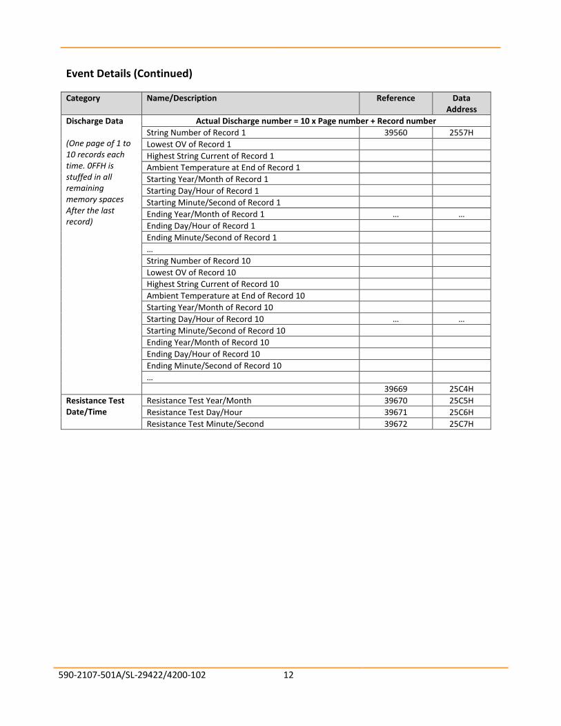
590-2107-501A/SL-29422/4200-102 12
Event Details (Continued)
Category Name/Description Reference Data Address
Discharge Data (One page of 1 to 10 records each time. 0FFH is stuffed in all remaining memory spaces After the last record)
Actual Discharge number = 10 x Page number + Record number
String Number of Record 1 39560 2557H
Lowest OV of Record 1
Highest String Current of Record 1
Ambient Temperature at End of Record 1
Starting Year/Month of Record 1
Starting Day/Hour of Record 1
Starting Minute/Second of Record 1
Ending Year/Month of Record 1 … …
Ending Day/Hour of Record 1
Ending Minute/Second of Record 1
…
String Number of Record 10
Lowest OV of Record 10
Highest String Current of Record 10
Ambient Temperature at End of Record 10
Starting Year/Month of Record 10
Starting Day/Hour of Record 10 … …
Starting Minute/Second of Record 10
Ending Year/Month of Record 10
Ending Day/Hour of Record 10
Ending Minute/Second of Record 10
…
39669 25C4H
Resistance Test Date/Time
Resistance Test Year/Month 39670 25C5H
Resistance Test Day/Hour 39671 25C6H
Resistance Test Minute/Second 39672 25C7H

590-2107-501A/SL-29422/4200-102 13
2.5 Configuration This section describes the details of the thresholds, resistance test interval, firmware commands, site
information, and remote password settings. For information on unit information details, refer to section
2.4. For additional information on Alarm type formats refer to section 4.1.
Category Name/Description Reference Data Address
Major Alarm Thresholds (Segmented array) Not recommend for new integration
High Cell Voltage Alarm Threshold 42754 0AC1H
Low Cell Voltage Alarm Threshold 42722 0AA1H
High Cell Resistance Alarm Threshold 42946 0B81H
Low Cell Resistance Alarm Threshold 42914 0B61H
High intercell Resistance Alarm Threshold 42978 0BA1H
High Cell Temperature Alarm Threshold 42850 0B21H
Low Cell Temperature Alarm Threshold 42786 0AE1H
High Ambient Temperature Alarm Threshold 42466 09A1H
Low Ambient Temperature Alarm Threshold 42402 0961H
High Overall Voltage Alarm Threshold 42562 0A01H
Low Overall Voltage Alarm Threshold 42530 09E1H
High String Current Alarm Threshold 42594 0A21H
High Ripple Current Alarm Threshold 42690 0A81H
High Float Current Alarm Threshold 42658 0A61H
Low Float Current Alarm Threshold 42626 0A41H
Cell to Ambient Temperature Deviation Threshold 43106 0C21H
Cell to Ambient Thermal Runaway Threshold 49711 25EEH
High Float Current Thermal Runaway Threshold 49712 25EFH
Discharge Trigger Current Threshold (Not for Alarm, used for discharge detection)
49713 25F0H
Ground Fault Resistance Positive Threshold (K)* 49705 25E8H
Ground Fault Resistance Negative Threshold (K)* 49706 25E9H
Ground Fault Current Threshold (future) 49714 25F1H
High Positive Charger Cable Resistance Alarm Threshold* 49720 25F7H
High Negative Charger Cable Resistance Alarm Threshold*
49721 25F8H
High Intertier Resistance Threshold 1 43010 0BC1H
High Intertier Resistance Threshold 2 43011 0BC2H
High Intertier Resistance Threshold 3 43012 0BC3H
High Intertier Resistance Threshold 4 43013 0BC4H
Major Alarm Thresholds (Sequential array) Only available in UXIM - 1.4.0 UXTM – 1.22.0 and after
High Cell Voltage Alarm Threshold 49134 23ADH
Low Cell Voltage Alarm Threshold 49135 23AEH
High Cell Resistance Alarm Threshold 49136 23AFH
Low Cell Resistance Alarm Threshold 49137 23B0H
High intercell Resistance Alarm Threshold 49138 23B1H
High Cell Temperature Alarm Threshold 49139 23B2H
Low Cell Temperature Alarm Threshold 49140 23B3H
High Ambient Temperature Alarm Threshold 49141 23B4H
Low Ambient Temperature Alarm Threshold 49142 23B5H
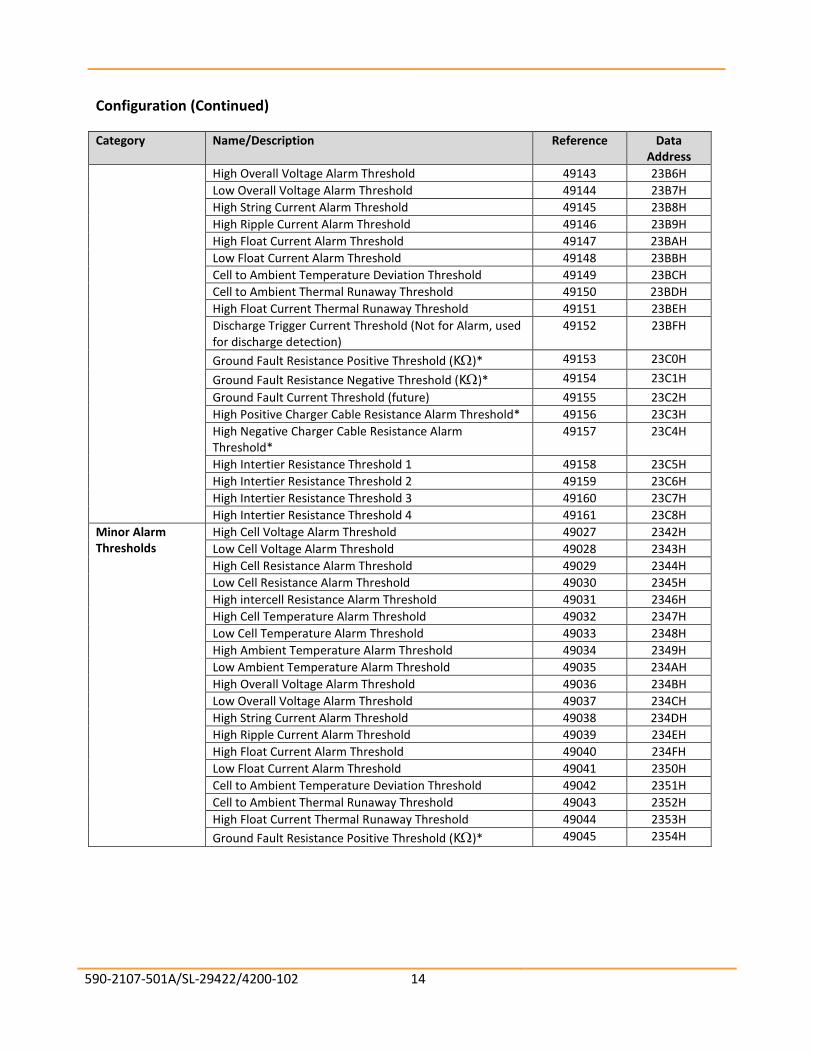
590-2107-501A/SL-29422/4200-102 14
Configuration (Continued)
Category Name/Description Reference Data Address
High Overall Voltage Alarm Threshold 49143 23B6H
Low Overall Voltage Alarm Threshold 49144 23B7H
High String Current Alarm Threshold 49145 23B8H
High Ripple Current Alarm Threshold 49146 23B9H
High Float Current Alarm Threshold 49147 23BAH
Low Float Current Alarm Threshold 49148 23BBH
Cell to Ambient Temperature Deviation Threshold 49149 23BCH
Cell to Ambient Thermal Runaway Threshold 49150 23BDH
High Float Current Thermal Runaway Threshold 49151 23BEH
Discharge Trigger Current Threshold (Not for Alarm, used for discharge detection)
49152 23BFH
Ground Fault Resistance Positive Threshold (K)* 49153 23C0H
Ground Fault Resistance Negative Threshold (K)* 49154 23C1H
Ground Fault Current Threshold (future) 49155 23C2H
High Positive Charger Cable Resistance Alarm Threshold* 49156 23C3H
High Negative Charger Cable Resistance Alarm Threshold*
49157 23C4H
High Intertier Resistance Threshold 1 49158 23C5H
High Intertier Resistance Threshold 2 49159 23C6H
High Intertier Resistance Threshold 3 49160 23C7H
High Intertier Resistance Threshold 4 49161 23C8H
Minor Alarm Thresholds
High Cell Voltage Alarm Threshold 49027 2342H
Low Cell Voltage Alarm Threshold 49028 2343H
High Cell Resistance Alarm Threshold 49029 2344H
Low Cell Resistance Alarm Threshold 49030 2345H
High intercell Resistance Alarm Threshold 49031 2346H
High Cell Temperature Alarm Threshold 49032 2347H
Low Cell Temperature Alarm Threshold 49033 2348H
High Ambient Temperature Alarm Threshold 49034 2349H
Low Ambient Temperature Alarm Threshold 49035 234AH
High Overall Voltage Alarm Threshold 49036 234BH
Low Overall Voltage Alarm Threshold 49037 234CH
High String Current Alarm Threshold 49038 234DH
High Ripple Current Alarm Threshold 49039 234EH
High Float Current Alarm Threshold 49040 234FH
Low Float Current Alarm Threshold 49041 2350H
Cell to Ambient Temperature Deviation Threshold 49042 2351H
Cell to Ambient Thermal Runaway Threshold 49043 2352H
High Float Current Thermal Runaway Threshold 49044 2353H
Ground Fault Resistance Positive Threshold (K)* 49045 2354H

590-2107-501A/SL-29422/4200-102 15
Configuration (Continued)
Category Name/Description Reference Data Address
Ground Fault Resistance Negative Threshold (K)* 49046 2355H
Ground Fault Current Threshold (future) 49047 2356H
High Positive Charger Cable Resistance Alarm Threshold* 49048 2357H
High Negative Charger Cable Resistance Alarm Threshold*
49049 2358H
High Intertier Resistance Threshold 1 49050 2359H
High Intertier Resistance Threshold 2 49051 235AH
High Intertier Resistance Threshold 3 49052 235BH
High Intertier Resistance Threshold 4 49053 235CH
Intertier Configuration
Intertier 1 Configuration String # (Byte 1) 49715 25F2H
Cell # (Byte 2)
Intertier 2 Configuration String # (Byte 1) 49716 25F3H
Cell # (Byte 2)
Intertier 3 Configuration String # (Byte 1) 49717 25F4H
Cell # (Byte 2)
Intertier 4 Configuration String # (Byte 1) 49718 25F5H
Cell # (Byte 2)
Enables Ambient Temperature Enable (A value of 0 means all ambient temperature sensors disabled. A value of N means Ambient Temperatures 1 to N are enabled.)
49719 25F6H
Resistance Test Interval
Resistance Test Period (Days) 49694 25DDH
Resistance Alarm Type
BIT0 = 1 Check resistance and intercell alarm using percentage change. = 0 Check resistance and intercell alarm using absolute value.
49062 2365H
Major High Alarm Enable
BIT0 = 1 Enable Cell Voltage BIT1 = 1 Enable String Voltage BIT2 = 1 Enable Float Current BIT3 = 1 Enable Ripple Current BIT4 = 1 Enable Cell Temperature BIT5 = 1 Enable Cell Resistance BIT6 = 1 Enable Intercell BIT7 = 1 Enable Discharge Current BIT8 = 1 Enable Charger Cable Resistance BIT9 = 1 Enable Digital Input BIT10: Reserved BIT11=1 Enable Ambient Temperature BIT12=1 Enable Intertier BIT13=1 Enable Cell to Ambient BIT14=1 Enable Thermal Runaway Cell to Ambient BIT15=1 Enable Thermal Runaway Float current
49063 2366H

590-2107-501A/SL-29422/4200-102 16
Configuration (Continued)
Category Name/Description Reference Data Address
Major Low Alarm Enable
BIT0 = 1 Enable Cell Voltage BIT1 = 1 Enable String Voltage BIT2 = 1 Enable Float Current BIT3 = 1 Enable Ripple Current BIT4 = 1 Enable Cell Temperature BIT5 = 1 Enable Cell Resistance BIT6: Reserved BIT7: Reserved BIT8: Reserved BIT9: Enable Digital Input BIT10 = 1 Enable Ground Fault BIT11=1 Enable Ambient Temperature BIT12=1 Enable Intertier BIT13–BIT15: Reserved
49064 2367H
Minor High Alarm Enable
BIT0 = 1 Enable Cell Voltage BIT1 = 1 Enable String Voltage BIT2 = 1 Enable Float Current BIT3 = 1 Enable Ripple Current BIT4 = 1 Enable Cell Temperature BIT5 = 1 Enable Cell Resistance BIT6 = 1 Enable Intercell BIT7 = 1 Enable Discharge Current BIT8 = 1 Enable Charger Cable Resistance BIT9 = 1 Enable Digital Input BIT10: Reserved BIT11=1 Enable Ambient Temperature BIT12=1 Enable Intertier BIT13=1 Enable Cell to Ambient BIT14=1 Enable Thermal Runaway Cell to Ambient BIT15=1 Enable Thermal Runaway Float current
49065 2368H

590-2107-501A/SL-29422/4200-102 17
Configuration (Continued)
Category Name/Description Reference Data Address
Minor Low Alarm Enable
BIT0 = 1 Enable Cell Voltage BIT1 = 1 Enable String Voltage BIT2 = 1 Enable Float Current BIT3 = 1 Enable Ripple Current BIT4 = 1 Enable Cell Temperature BIT5 = 1 Enable Cell Resistance BIT6: Reserved BIT7: Reserved BIT8: Reserved BIT9 = 1 Enable Digital Input BIT10 = 1 Enable Ground Fault BIT11=1 Enable Ambient Temperature BIT12=1 Enable Intertier BIT13–BIT15: Reserved
49066 2369H
Major High Alarm Latch
BIT0 = 1 Latch Cell Voltage BIT1 = 1 Latch String Voltage BIT2 = 1 Latch Float Current BIT3 = 1 Latch Ripple Current BIT4 = 1 Latch Cell Temperature BIT5 = 1 Latch Cell Resistance BIT6 = 1 Latch Intercell BIT7 = 1 Latch Discharge Current BIT8 = 1 Latch Charger Cable Resistance BIT9 = 1 Latch Digital Input BIT10: Reserved BIT11=1 Latch Ambient Temperature BIT12=1 Latch Intertier BIT13=1 Enable Cell to Ambient BIT14=1 Enable Thermal Runaway Cell to Ambient BIT15=1 Enable Thermal Runaway Float current
49067 236AH

590-2107-501A/SL-29422/4200-102 18
Configuration (Continued)
Category Name/Description Reference Data Address
Major Low Alarm Latch
BIT0 = 1 Latch Cell Voltage BIT1 = 1 Latch String Voltage BIT2 = 1 Latch Float Current BIT3 = 1 Latch Ripple Current BIT4 = 1 Latch Cell Temperature BIT5 = 1 Latch Cell Resistance BIT6: Reserved BIT7: Reserved BIT8: Reserved BIT9: Latch Digital Input BIT10 = 1 Latch Ground Fault BIT11=1 Latch Ambient Temperature BIT12=1 Latch Intertier BIT13–BIT15: Reserved
49068 236BH
Minor High Alarm Latch
BIT0 = 1 Latch Cell Voltage BIT1 = 1 Latch String Voltage BIT2 = 1 Latch Float Current BIT3 = 1 Latch Ripple Current BIT4 = 1 Latch Cell Temperature BIT5 = 1 Latch Cell Resistance BIT6 = 1 Latch Intercell BIT7 = 1 Latch Discharge Current BIT8 = 1 Latch Charger Cable Resistance BIT9 = 1 Latch Digital Input BIT10: Reserved BIT11=1 Latch Ambient Temperature BIT12=1 Latch Intertier BIT13=1 Enable Cell to Ambient BIT14=1 Enable Thermal Runaway Cell to Ambient BIT15=1 Enable Thermal Runaway Float current
49069 236CH

590-2107-501A/SL-29422/4200-102 19
Configuration (Continued)
Category Name/Description Reference Data Address
Minor Low Alarm Latch
BIT0 = 1 Latch Cell Voltage BIT1 = 1 Latch String Voltage BIT2 = 1 Latch Float Current BIT3 = 1 Latch Ripple Current BIT4 = 1 Latch Cell Temperature BIT5 = 1 Latch Cell Resistance BIT6: Reserved BIT7: Reserved BIT8: Reserved BIT9 = 1 Latch Digital Input BIT10 = 1 Latch Ground Fault BIT11=1 Latch Ambient Temperature BIT12=1 Latch Intertier BIT13–BIT15: Reserved
49070 236DH
*UXIM only
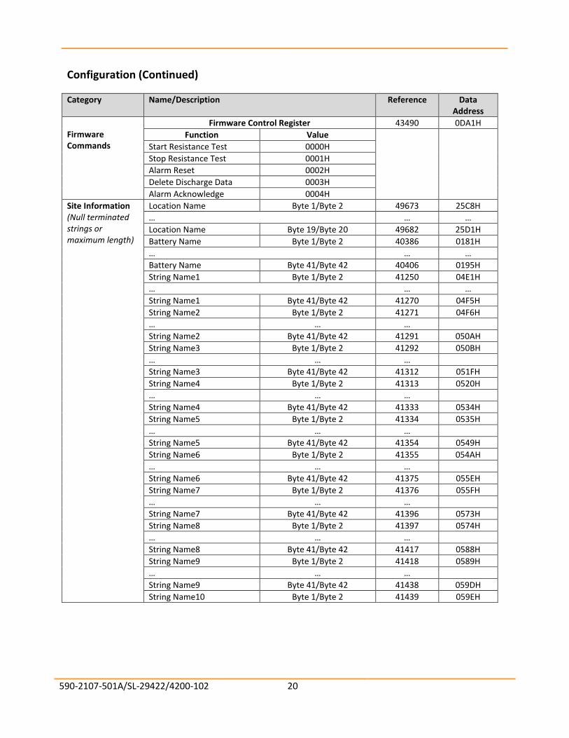
590-2107-501A/SL-29422/4200-102 20
Configuration (Continued)
Category Name/Description Reference Data Address
Firmware Commands
Firmware Control Register 43490 0DA1H
Function Value
Start Resistance Test 0000H
Stop Resistance Test 0001H
Alarm Reset 0002H
Delete Discharge Data 0003H
Alarm Acknowledge 0004H
Site Information (Null terminated strings or maximum length)
Location Name Byte 1/Byte 2 49673 25C8H
… … …
Location Name Byte 19/Byte 20 49682 25D1H
Battery Name Byte 1/Byte 2 40386 0181H
… … …
Battery Name Byte 41/Byte 42 40406 0195H
String Name1 Byte 1/Byte 2 41250 04E1H
… … …
String Name1 Byte 41/Byte 42 41270 04F5H
String Name2 Byte 1/Byte 2 41271 04F6H
… … …
String Name2 Byte 41/Byte 42 41291 050AH
String Name3 Byte 1/Byte 2 41292 050BH
… … …
String Name3 Byte 41/Byte 42 41312 051FH
String Name4 Byte 1/Byte 2 41313 0520H
… … …
String Name4 Byte 41/Byte 42 41333 0534H
String Name5 Byte 1/Byte 2 41334 0535H
… … …
String Name5 Byte 41/Byte 42 41354 0549H
String Name6 Byte 1/Byte 2 41355 054AH
… … …
String Name6 Byte 41/Byte 42 41375 055EH
String Name7 Byte 1/Byte 2 41376 055FH
… … …
String Name7 Byte 41/Byte 42 41396 0573H
String Name8 Byte 1/Byte 2 41397 0574H
… … …
String Name8 Byte 41/Byte 42 41417 0588H
String Name9 Byte 1/Byte 2 41418 0589H
… … …
String Name9 Byte 41/Byte 42 41438 059DH
String Name10 Byte 1/Byte 2 41439 059EH
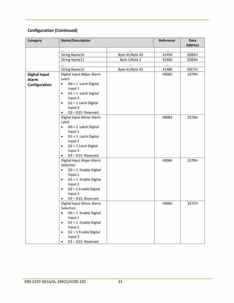
590-2107-501A/SL-29422/4200-102 21
Configuration (Continued)
Category Name/Description Reference Data Address
… … …
String Name10 Byte 41/Byte 42 41459 05B2H
String Name11 Byte 1/Byte 2 41460 05B3H
… … …
String Name12 Byte 41/Byte 42 41480 05C7H
Digital Input Alarm Configuration
Digital Input Major Alarm Latch
• D0 = 1 Latch Digital Input 1
• D1 = 1 Latch Digital Input 2
• D2 = 1 Latch Digital Input 3
• D3 – D15: Reserved
49082 2379H
Digital Input Minor Alarm Latch
• D0 = 1 Latch Digital Input 1
• D1 = 1 Latch Digital Input 2
• D2 = 1 Latch Digital Input 3
• D3 – D15: Reserved
49083 237AH
Digital Input Major Alarm Selection
• D0 = 1 Enable Digital Input 1
• D1 = 1 Enable Digital Input 2
• D2 = 1 Enable Digital Input 3
• D3 – D15: Reserved
49084 237BH
Digital Input Minor Alarm Selection
• D0 = 1 Enable Digital Input 1
• D1 = 1 Enable Digital Input 2
• D2 = 1 Enable Digital Input 3
• D3 – D15: Reserved
49085 237CH

590-2107-501A/SL-29422/4200-102 22
Configuration (Continued)
Category Name/Description Reference Data Address
Digital Input Open/Close 1: Normal Open 0: Normal Close
• D0: Digital Input 1
• D1: Digital Input 2
• D2: Digital Input 3
• D3 – D15: Reserved
49086 237DH
Digital Input Name
Digital Input Name1 Byte 1/Byte 2 49087 237EH
…
Digital Input Name1 Byte 19/Byte 20 49096 2387H
Digital Input Name2 Byte 1/Byte 2 49097 2388H
…
Digital Input Name2 Byte 19/Byte 20 49106 2391H
Digital Input Name3 Byte 1/Byte 2 49107 2392H
…
Digital Input Name3 Byte 19/Byte 20 49116 239BH
String Name13 Byte 1/Byte 2 41481 05C8H
… … …
String Name13 Byte 41/Byte 42 41501 05DCH
String Name14 Byte 1/Byte 2 41502 05DDH
… … …
String Name14 Byte 41/Byte 42 41522 05F1H
String Name15 Byte 1/Byte 2 41523 05F2H
… … …
String Name15 Byte 41/Byte 42 41543 0606H
String Name16 Byte 1/Byte 2 41544 0607H
… … …
String Name16 Byte 41/Byte 42 41564 061BH
Remote Password (Null terminated or maximum length)
Password 1 Byte 1/Byte 2 49683 25D2H
Password 1 Byte 3/Byte 4 49684 25D3H
Password 1 Byte 5/ Byte 6 49685 25D4H
590-2107-501A/SL-29422/4200-102 23
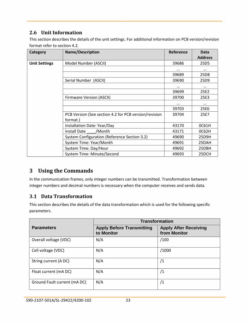
2.6 Unit Information This section describes the details of the unit settings. For additional information on PCB version/revision
format refer to section 4.2.
Category Name/Description Reference Data Address
Unit Settings Model Number (ASCII) 39686 25D5
… …
39689 25D8
Serial Number (ASCII) 39690 25D9
… …
39699 25E2
Firmware Version (ASCII) 39700 25E3
… …
39703 25E6
PCB Version (See section 4.2 for PCB version/revision format.)
39704 25E7
Installation Date: Year/Day 43170 0C61H
Install Date ____/Month 43171 0C62H
System Configuration (Reference Section 3.2) 49690 25D9H
System Time: Year/Month 49691 25DAH
System Time: Day/Hour 49692 25DBH
System Time: Minute/Second 49693 25DCH
3 Using the Commands
In the communication frames, only integer numbers can be transmitted. Transformation between
integer numbers and decimal numbers is necessary when the computer receives and sends data.
3.1 Data Transformation
This section describes the details of the data transformation which is used for the following specific
parameters.
Parameters
Transformation
Apply Before Transmitting to Monitor
Apply After Receiving from Monitor
Overall voltage (VDC) N/A /100
Cell voltage (VDC) N/A /1000
String current (A DC) N/A /1
Float current (mA DC) N/A /1
Ground Fault current (mA DC) N/A /1
590-2107-501A/SL-29422/4200-102 24
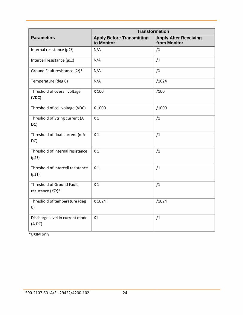
Parameters
Transformation
Apply Before Transmitting to Monitor
Apply After Receiving from Monitor
Internal resistance () N/A /1
Intercell resistance () N/A /1
Ground Fault resistance ()* N/A /1
Temperature (deg C) N/A /1024
Threshold of overall voltage
(VDC)
X 100 /100
Threshold of cell voltage (VDC) X 1000 /1000
Threshold of String current (A
DC)
X 1 /1
Threshold of float current (mA
DC)
X 1 /1
Threshold of internal resistance
()
X 1 /1
Threshold of intercell resistance
()
X 1 /1
Threshold of Ground Fault
resistance (K)*
X 1 /1
Threshold of temperature (deg
C)
X 1024 /1024
Discharge level in current mode
(A DC)
X1 /1
*UXIM only

590-2107-501A/SL-29422/4200-102 25
3.2 System Configurations
This section describes the details of the system configuration types.
Technology
Battery/String configuration
(number of strings X number of data points X
Nominal voltage of data point)
Configuration
Number
1V – NiCad Cells (24V) 1X18X1V 0
2V Cells (24V) 1X12X2V 1
2V Cells (24V) 2X12X2V 2
2V Cells (48V) 1X24X2V 3
4V Mono-Blocks (24V)
1X6X4V 4
2X6X4V 5
3X6X4V 6
4X6X4V 7
4V Mono-Blocks (48V) 1X12X4V 8
2X12X4V 9
6V Mono-Blocks (24V)
1X4X6V 10
2X4X6V 11
3X4X6V 12
4X4X6V 13
6V Mono-Blocks (48V)
1X8X6V 14
2X8X6V 15
3X8X6V 16
8V Mono-Blocks (24V)
1X3X8V 17
2X3X8V 18
3X3X8V 19
4X3X8V 20

590-2107-501A/SL-29422/4200-102 26
System Configurations (Continued)
Technology
Battery/String configuration
(number of strings X number of data points X
Nominal voltage of data point)
Configuration
Number
8V Mono-Blocks (48V)
1X6X8V 21
2X6X8V 22
3X6X8V 23
4X6X8V 24
12V Mono-Blocks (24V)
1X2X12V 25
2X2X12V 26
3X2X12V 27
4X2X12V 28
12V Mono-Blocks (48V)
1X4X12V 29
2X4X12V 30
3X4X12V 31
4X4X12V 32
16V Mono-Blocks (48V)
1X3X16V 33
2X3X16V 34
3X3X16V 35
4X3X16V 36

590-2107-501A/SL-29422/4200-102 27
4 Alarm Type and PCB Revision/Version Format Appendix This section describes the details of the alarm type, and PCB revision format settings.
4.1 Alarm Type Format
Data BIT Location and Meaning
D15 D14 D13 D12 D11 D10 D9 D8 D7 D6 D5 D4 D3 D2 D1 D0
Parameter Alarm Status String number (0 – 15) Cell number (0 – 127); For Battery System Ground Fault Resistance: 0 = Positive, 1 = Negative
Parameter Name Value
Cell voltage 0 Cell temperature 1 Cell resistance 2 Cell intercell 3 Overall voltage 4 String current 5 Float current 6 Ripple current 7 Ambient temperature 8 Cell to ambient Intertier Cell to ambient thermal runaway High float current thermal runaway Ground fault Charger Cable resistance
9 10 11 12 13 14
Digital Input 15
Alarm Status
State Value
High alarm 1 Low alarm 0

590-2107-501A/SL-29422/4200-102 28
4.2 PCB version/revision format
Data BIT Location and Meaning
Base revision Sub revision
D7 D6 D5 D4 D3 D2 D1 D0
Value 0 – ‘A’ 1 – ‘B’ 2 – ‘C’ 3 – ‘D’ 4 – ‘E’ 5 – ‘F’ 6 – ‘G’ 7 – ‘H’
0 - 15