maciej gołaszewski tutor: tadeusz sondej, phd design and implementation of softcore dual processor...
TRANSCRIPT
Maciej Gołaszewski
Tutor: Tadeusz Sondej, PhD
Design and implementation
of softcore dual processor system
on single chip FPGA
Design and implementation
of softcore dual processor system
on single chip FPGA
Military Universityof Technology
Faculty of ElectronicsInstitute of Telecommunication
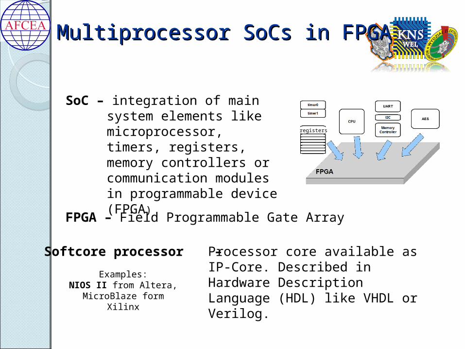
Multiprocessor Multiprocessor SoCs iSoCs in FPGAn FPGA
Processor core available as IP-Core. Described in Hardware Description Language (HDL) like VHDL or Verilog.
Softcore processor –
Examples:NIOS II from Altera,
MicroBlaze form Xilinx
SoC – integration of main system elements like microprocessor, timers, registers, memory controllers or communication modules in programmable device (FPGA)
FPGA – Field Programmable Gate Array
registers

Processor communicationProcessor communication
Shared memory (SM) all processors have
common address space processors can have
own local memory (M) to communicate
processors modify data in shared memory
Message passing processors have
separate address space communication is
realized by sending messages
processors are directly connected
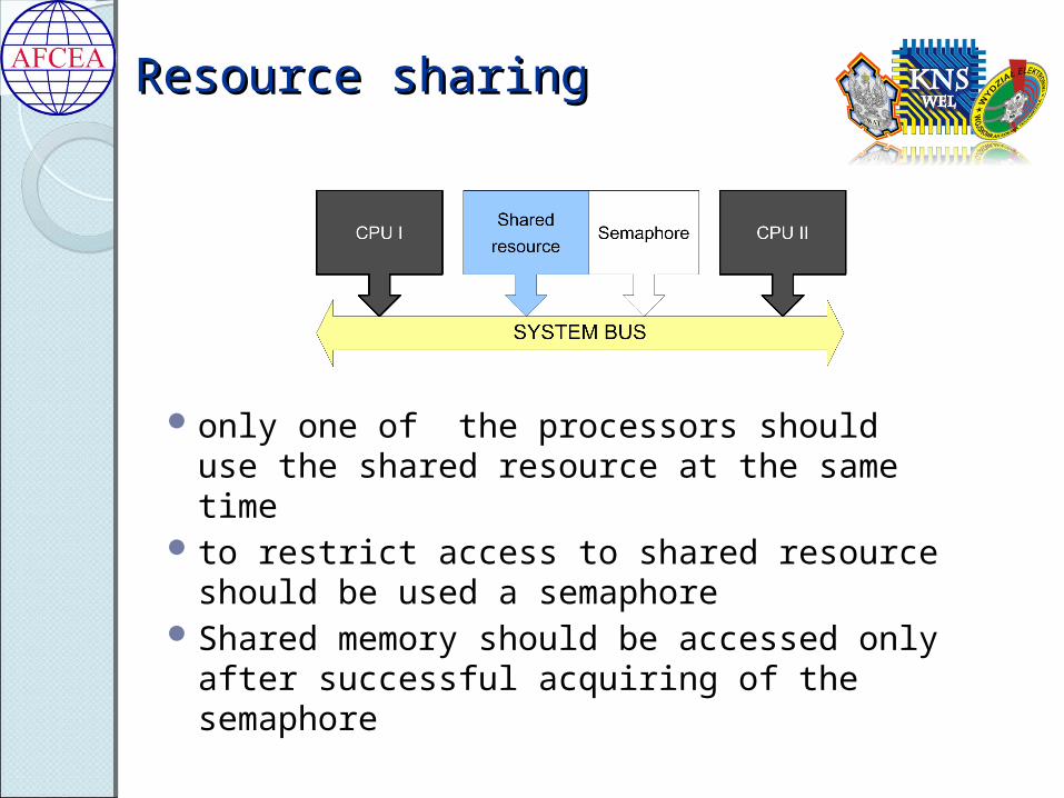
Resource sharingResource sharing
only one of the processors should use the shared resource at the same time
to restrict access to shared resource should be used a semaphore
Shared memory should be accessed only after successful acquiring of the semaphore
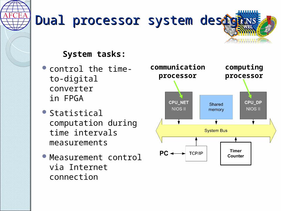
Dual processor system designDual processor system design
System tasks:
control the time-to-digital converterin FPGA
Statistical computation during time intervals measurements
Measurement control via Internet connection
communicationprocessor
computingprocessor

Time-to-digital converterTime-to-digital converter
32 binary counters counting periods of 16-phase clockof the 400 MHz frequency (both edges of clock are active)
equivalent of a single clock signal of 12.8 GHz frequency
provides 78 ps resolution in a single stage interpolation
measurement range 164 μs can be easily extended

SystemSystem hardware hardware overviewoverview
communicationprocessor
computingprocessor
FPGA device: Stratix II EP2S60 (Altera)

Hardware implementationHardware implementation
Nios II Developement Kit Stratix II Edition
FPGA device: Stratix II EP2S60 (Altera)
Flash 16MB
DDR SDRAM32MB
SSRAM 2MB
UARTEthernetJTAG
LEDsPush buttons prototype connectors

SoftwareSoftware
TCP/IP stack implemantationfrom InterNiche – NicheStack
Real-time operating system (RTOS) for embedded devices – µC/OS-II
Multithreaded application
Code optimized for statistical computation
Time-to-digital converter software drivers
Single threaded application

Host PC applicationHost PC application
Programming language: JAVA
Measurement control via Internet connection.
Measurement result display.
Measurement series histogram presentation.

ConclusionConclusion
Resource 2uP System2uP System
+ Timer CounterAvailable in Stratix II
ALUT 5 120 6 364 48 352
Registers 3 392 4 228 48 352
DSP blocks 16 16 288
Memory bits 126 464 126 464 2 544 192
PLL’s 1 5 6
FPGA resource utilization
Small resource utilization – 13% of Stratix II EPS2S60.
System clock – 100 MHz
Computing power of one processor is reservedonly for statistical computation.
Measurement control via Internet connection.

Maciej Gołaszewski
Thank you for your attention