design and implementation of a multithreaded softcore
TRANSCRIPT
Graduate Theses, Dissertations, and Problem Reports
2008
Design and implementation of a multithreaded softcore processor Design and implementation of a multithreaded softcore processor
with tightly coupled hardware real-time operating system with tightly coupled hardware real-time operating system
Terance Prabhasara Wijesinghe West Virginia University
Follow this and additional works at: https://researchrepository.wvu.edu/etd
Recommended Citation Recommended Citation Wijesinghe, Terance Prabhasara, "Design and implementation of a multithreaded softcore processor with tightly coupled hardware real-time operating system" (2008). Graduate Theses, Dissertations, and Problem Reports. 2682. https://researchrepository.wvu.edu/etd/2682
This Thesis is protected by copyright and/or related rights. It has been brought to you by the The Research Repository @ WVU with permission from the rights-holder(s). You are free to use this Thesis in any way that is permitted by the copyright and related rights legislation that applies to your use. For other uses you must obtain permission from the rights-holder(s) directly, unless additional rights are indicated by a Creative Commons license in the record and/ or on the work itself. This Thesis has been accepted for inclusion in WVU Graduate Theses, Dissertations, and Problem Reports collection by an authorized administrator of The Research Repository @ WVU. For more information, please contact [email protected].
Design and Implementation of a Multithreaded Softcore Processor with
Tightly Coupled Hardware Real-Time Operating System
Terance Prabhasara Wijesinghe
Thesis Submitted to the
College of Engineering and Mineral Resources
at West Virginia University
In partial fulfillment of the requirements
for the degree of
Master of Science
in
Electrical Engineering
Powsiri Klinkhachorn, Ph.D., Chair
Roy S. Nutter, Ph.D.
Afzel Noore, Ph.D.
David W. Graham, Ph.D.
Lane Department of Computer Science and Electrical Engineering
Morgantown, West Virginia
2008
Keywords: Hardware RTOSs, RTOSs, Softcore Processors, Multithreaded
Processors, FPGAs
Copyright 2008 Terance P. Wijesinghe
ii
Abstract
Design and Implementation of a Multithreaded Softcore Processor with Tightly
Coupled Hardware Real-Time Operating System
Terance Prabhasara Wijesinghe
The objective of this thesis is to design and implement an FPGA-based softcore
processor with hardware Real Time Operating System (RTOS). RTOSs provide an abstracted environment on top of the hardware with different
mechanisms to simplify and coordinate the behavior of the system. Software mechanisms including multithreading, semaphores, timers, interrupts, etc. consume large amounts of CPU time which increases overhead and contributes to the degradation of the performance. In order to offload this overhead, RTOSs with hardware acceleration have been a research topic with considerable interest. Most research works are focused on the design of a hardware RTOS external to the CPU where CPU interacts with the hardware RTOS module as a memory mapped device. This approach provides the flexibility of using the general purpose processor, however, fast context switching is not possible unless a special CPU with a duplicated register file is equipped. To this end, tightly coupling the RTOS functionality to the CPU pipeline is a good candidate for further investigation. Multithreaded processors are a distinct area of research focusing on reducing the pipeline hazards by interleaving instructions from different threads. Most of the multithreading techniques support fast context switching mechanisms in order to support cycle interleaving of instructions. The fast context switching ability inherent to multithreaded processors can be used to implement OS level multithreading and low latency interrupt service threads. This thesis investigates on the possibilities of merging previous research work on hardware RTOSs and multithreaded processors to obtain an overall improvement. Attachment of a hardware RTOS to the pipeline increases the determinism by eliminating external interfaces with nondeterministic bus arbitration schemes and reduces the logic required to implement the external interfaces.
The implemented prototype processor is instruction set compatible with Xilinx Microblaze and has a five stage multithreaded pipeline. The pipeline is extended with a static priority preemptive scheduler, semaphore and timer modules. The instruction set is augmented with several instructions to support thread creation, deletion, synchronization and time management. Results suggest that RTBlaze can completely remove the OS overhead at the cost of doubled processor size. Zero overhead scheduler, context switching, thread synchronization, timers and five-cycle interrupt latency give excellent performance as well as the increased determinism compared with software RTOSs.

iii
Acknowledgements
I would first like to thank my advisor Dr. Powsiri Klinkhachorn for the support and
guidance he has given me during my two years as a graduate student. I am also grateful
to Dr. David W. Graham, Dr. Roy S. Nutter and Dr. Afzel Noore for their support.
I take this opportunity to thank my parents and sister for supporting and guiding me
in my decisions. I am also thankful to all those who helped me directly or indirectly in
completion of this work.
Prabhasara Wijesinghe
iv
Contents
Abstract ..............................................................................................................................ii
Acknowledgements...........................................................................................................iii
Contents ............................................................................................................................ iv
List of Figures and Illustrations ........................................................................................vi
List of Tables ..................................................................................................................viii
List of Symbols, Abbreviations and Nomenclature .......................................................... ix
Chapter 1. Introduction ...................................................................................................... 1
1.1 Motivation............................................................................................................... 1
1.2 Objective ................................................................................................................. 3
1.3 Thesis contribution.................................................................................................. 4
1.4 Thesis outline .......................................................................................................... 4
Chapter 2. Literature Review............................................................................................. 5
2.1 Field Programmable Gate Arrays ........................................................................... 5
2.2 Platform FPGAs - Vertex II Pro ............................................................................. 8
2.3 Systems on a Programmable Chip (SoPC) Design ............................................... 10
2.4 Configurable Softcore Processors for FPGAs ...................................................... 14
2.5 Real-time Operating Systems for SoPC Based Systems....................................... 15
2.6 Multithreaded Processors...................................................................................... 17
2.7 Hardware Support for Operating Systems ............................................................ 20
2.8 Processors with OS Level Support........................................................................ 23

v
Chapter 3. Design and Implementation of the RTBlaze .................................................. 26
3.1 Design of the Base Processor................................................................................. 27
3.1.1 First Stage – Instruction Fetch ..................................................................... 33
3.1.2 Second Stage – Instruction Decode ............................................................. 34
3.1.3 Third Stage – Instruction Execute................................................................ 38
3.1.4 Fourth Stage – Data Memory Access .......................................................... 40
3.1.5 Fifth Stage – Result Write Back .................................................................. 42
3.1.6 Hazard Resolution........................................................................................ 43
3.2 Architecture of RTOS ............................................................................................ 46
3.3 Design of the RTBlaze........................................................................................... 51
3.3.1 The Fetch Stage with Scheduling Support ................................................... 56
3.3.2 Support for Interrupt Service Threads ......................................................... 59
3.3.3 Hardware Timers.......................................................................................... 60
3.3.4 Hardware Semaphores ................................................................................. 61
3.4 Implementation and Performance of the RTBlaze................................................ 64
Chapter 4. Results ............................................................................................................ 66
4.1 Simulation Results ................................................................................................ 66
4.1.1 Base Processor Validation ........................................................................... 67
4.1.2 RTBlaze Validation...................................................................................... 78
4.2 Performance Comparison...................................................................................... 92
4.2.1 Comparison of the Performance of RTBlaze and Software RTOSs............ 93
4.3 Size of the Kernel Footprint.................................................................................. 94
4.4 Analysis of Area Overhead ................................................................................... 95
Chapter 5. Conclusions and Future Work........................................................................ 97
5.1 Conclusions........................................................................................................... 97
5.2 Future Work .......................................................................................................... 99
References ...................................................................................................................... 101
vi
List of Figures and Illustrations
Figure 2.1: Simplified Internal Architecture of an FPGA ................................................. 7
Figure 2.2: Generic Logic Element.................................................................................... 7
Figure 2.3: Internal Architecture of Vertex II Pro Platform FPGA [16] ........................... 9
Figure 2.4: Local Interconnects of the Slices in a Single CLB [16] ................................ 10
Figure 2.5: CoreConnect Based SoPC System [22]......................................................... 11
Figure 2.6: Xilinx ISE FPGA Design Flow [26] ............................................................. 12
Figure 2.7: Xilinx Embedded Development Kit Design Flow [17]................................. 13
Figure 2.8: 32-Bit Microblaze Soft Processor [15].......................................................... 16
Figure 2.9: Pipeline Hazards Due to Data Dependencies ................................................ 18
Figure 2.10: RAW Hazard Resolution with Data Forwarding......................................... 18
Figure 3.1: EDK Integration of the Base Processor......................................................... 28
Figure 3.2: The Five Stage Pipeline................................................................................. 28
Figure 3.3: Block Diagram of the Proposed Base Processor ........................................... 29
Figure 3.4: The Instruction Formats ................................................................................ 29
Figure 3.5: Simplified Five Stage Pipeline of the Base Processor................................... 31
Figure 3.6: Instruction Fetch Stage .................................................................................. 33
Figure 3.7: LMB Single Read Transaction [15] .............................................................. 34
Figure 3.8: Control Signal Flow in the Pipeline .............................................................. 35
Figure 3.9: Register File with Three Read Ports and One Write Port ............................. 37
Figure 3.10: Branch Resolution Logic............................................................................. 39
Figure 3.11: Execution Stage ........................................................................................... 40
Figure 3.12: Read Data Steering ...................................................................................... 42
Figure 3.13: Base Processor Pipeline with Hazard Control............................................. 45
Figure 3.14: State Transition Diagram of a Thread ......................................................... 48
Figure 3.15: Simplified Architecture of a RTOS Kernel Running On a SOPC............... 49
Figure 3.16: Base Processor with RTOS Extension ........................................................ 53
Figure 3.17: State Transition Diagram of an RTBlaze Thread ........................................ 54
Figure 3.18: Multithread Pipeline with Scheduling Support ........................................... 55
Figure 3.19: Microarchitecture of the Static Priority Based Thread Scheduler............... 57

vii
Figure 3.20: Modified Prefetch Stage with Scheduling Support ..................................... 58
Figure 3.21: Extension of the Scheduler to Support Hardware ISTs............................... 59
Figure 3.22: Direct Mapped Hardware Timers ............................................................... 61
Figure 3.23: Microarchitecture of a Single Hardware Semaphore .................................. 62
Figure 3.24: Microarchitecture of a Single Priority Queue Element ............................... 64
Figure 4.1: Sample Program- Simulation Results (80ns to 190ns) Part I ........................ 68
Figure 4.2: Sample Program - Simulation Results (80ns to 190ns) Part II...................... 69
Figure 4.3: Sample Program - Simulation Results (180ns to 290ns) Part I ..................... 70
Figure 4.4: Sample Program - Simulation Results (180ns to 290ns) Part II.................... 71
Figure 4.5: Load/Store Instructions - Simulation Results (30ns To 130ns) Part I........... 75
Figure 4.6: Load/Store Instructions - Simulation Results (30ns to 130ns) Part II........... 76
Figure 4.7: Simulation Results and Pipeline Events - Thread Creation........................... 79
Figure 4.8: Execution of Sleep Instruction – Thread 2 Sleeps for Five Cycles............... 81
Figure 4.9: Simulation Results and Pipeline Events - Creation of a New IST ............... 85
Figure 4.10: Simulation Results and Pipeline Events – External Interrupt ..................... 86
Figure 4.11: Simulation Results and Pipeline Events – Interrupt Clear .......................... 87
Figure 4.12: Semaphore Instructions - Simulation Results (580ns to 680ns) Part I........ 89
Figure 4.13: Semaphore Instructions - Simulation Results (680ns to 780ns) Part II....... 90
viii
List of Tables
Table 3.1: A Partial List of Microblaze Instruction Set ................................................... 30
Table 3.2: Flow of Control Signals through Each Pipeline Stage ................................... 36
Table 3.3: Operations Supported by the ALU ................................................................. 38
Table 3.4: Conditional Control Transfer Instructions...................................................... 39
Table 3.5: Load Store Instructions................................................................................... 41
Table 3.6: Read Data Steering [15].................................................................................. 41
Table 3.7: Write Data Steering [15]................................................................................. 42
Table 3.8: RAW Hazards in Progress .............................................................................. 43
Table 3.9: Hazard Resolution........................................................................................... 44
Table 3.10: Basic System Calls Provided by a RTOS ..................................................... 46
Table 3.11: RTBlaze Instructions for RTOS Services..................................................... 52
Table 4.1: Assembly Program Used to Validate Arithmetic and Branch Instructions .... 67
Table 4.2: Execution of the Program – Pipeline Events during the First Iteration .......... 72
Table 4.3: Execution of the Program – Pipeline Events during the Last Iteration .......... 73
Table 4.4: Program to Validate Data Memory Access .................................................... 74
Table 4.5: Execution of Load\Store Instructions– Pipeline Events ................................. 77
Table 4.6: Thread Creation ............................................................................................. 78
Table 4.7: Thread Sleep ................................................................................................... 80
Table 4.8: Execution of Sleep Instruction – Pipeline Events........................................... 82
Table 4.9: A Program to Validate the IST Mechanism.................................................... 84
Table 4.10: A Program to Validate Semaphore Operations............................................. 88
Table 4.11: Execution of Semaphore Instructions– Pipeline Events ............................... 91
Table 4.12: Latencies ....................................................................................................... 94
Table 4.13: Kernel Footprint Comparison ....................................................................... 94
Table 4.14: Resource Utilization Of RTOS Extensions .................................................. 95
Table 4.15: Breakdown of Area Overhead Due to RTOS Extensions............................. 96
ix
List of Symbols, Abbreviations and Nomenclature
FPGA Field Programmable Gate Array
SOPC System on a Programmable Chip
ADL Architectural Definition Language
VHDL Very high speed Hardware Description Language
PLB Processor Local Bus
OPB On Chip Peripheral Bus
IP Intellectual Property
SoC System on a Chip
RTOS Real-time Operating System
OS Operating System
LVTTL Low Voltage Transistor Transistor Logic
LVCMOS Low Voltage Complementary Metal Oxide
Semiconductor
CLB Configurable Logic Block
FSL Fast Simplex Link
LUT Look Up Table
JTAG Joint Test Action Group
EDF Earliest deadline First
LMB Local Memory Bus
TSS Task State Segment
IST Interrupt Service Thread
GCC GNU Compiler Collection
TCB Task Control Block
DCR Device Control Register
1
Chapter 1
Introduction
1.1 Motivation
Embedded systems have become omnipresent, and most of them have real-time
behavior. Unlike general purpose systems, deadlines are not relaxed and determinism is
a very important aspect. These systems are supposed to meet given deadlines and a
missed deadline may even be catastrophic.
For the high performance hard real-time systems the overhead of operating system
cannot be neglected. The Operating System (OS) scheduler and context switching
overhead collectively consume the useful CPU time. Interrupt processing overhead
contributes to the interrupt latency and in turn reduces the system response time. In order
to offload these overheads, real-time operating systems with hardware acceleration have
been a research topic with considerable interest.
2
Before the Field Programmable Gate Array (FPGA) based configurable embedded
systems enter the mainstream, all of the research work on hardware-based acceleration
of OSs are focused on silicon implementations [1-4]. To support OS primitives at the
hardware level, several research groups have made efforts to implement OSs on silicon.
These are separate chips or Intellectual Property (IP) cores connected to the external
CPU bus as memory mapped peripherals enabling the use of general purpose CPUs.
Most research groups have focused on only the scheduler component design in
hardware, since most real-time systems demand complicated schedulers and most of
those algorithms have the property of paralizability where the hardware implementation
is the ideal solution [3, 5-7]. The external chip based hardware scheduler performs the
timekeeping and the scheduling and raises an interrupt to the CPU in case preemption is
required. Upon interruption, the CPU communicates with the hardware scheduler,
obtains the next thread ID, and performs a context switch. This method off-loads the
kernel timer tick counting and execution of the scheduler. Not only the scheduler, but
also RTOS functionality such as timers and semaphores are excellent candidates for
hardware migration [1, 4]. All the previous researchers have proven that the hardware
implementations give promising results over the software-based conventional RTOS
implementations.
Intellectual Property (IP) or separate chip based approach gives the flexibility of
using a general purpose processor, but determinism is again sacrificed due to
nondeterministic bus arbitration schemes equipped in Systems on a Programmable Chip
(SoPC) architectures. Round robin bus arbitration makes it feasible to have a
deterministic way of interacting with IP services, but it degrades the overall system
performance. One way to overcome this issue is to attach the IP as a coprocessor with
special bus interface [8]; however, these methods are not capable of removing the
context switching overhead. In order to remove the overhead due to context switching, a
special CPU has to be used with a dedicated interface with the hardware scheduler [9].
One method is to use a register file with a transparent loading mechanism of the context
of the thread in the background. To this end, tightly coupling the RTOS functionality to
the processor itself is a good candidate for further investigation.
3
Multithreaded processors are a distinct area of research focusing on reducing the
pipeline hazards by interleaving instructions from different threads [10]. Multithreading
comes in three different flavors: cycle interleaved, block interleaved, and hybrid. Cycle
interleaved multithreaded processors inherit a special feature of switching the thread
contexts in a single cycle. This interesting feature can be used to eliminate the overhead
due to context switching in the OS domain. There are some research proposals to utilize
this fast context switching ability to implement fast interrupt service threads [11-14].
This thesis investigates on the possibilities of merging these two orthogonally
investigated concepts of multithreaded processors and hardwired RTOS implementations
to obtain an overall improvement. Multithreaded pipeline provides zero overhead
context switching as well as low latency interrupt handling mechanism, while the
hardware migrated RTOS functionality provides low overhead thread, timer and
semaphore manipulation. Attachment of hardware RTOS to the pipeline increases the
determinism by eliminating external interfaces where the arbitration is an issue.
1.2 Objective
The objective of this thesis is to design and implement a prototype 32 bit RISC
multithreaded processor, RTBlaze, with tightly coupled hardware RTOS attached to its
pipeline. The first phase of this thesis designs a base processor instruction set compatible
with Xilinx MicroBlaze [15].
The second phase of this thesis extends the base processor with hardware RTOS
support. The base processor pipeline is extended to support cycle and block interleaved
multithreading. A special thread scheduler in the fetch stage decides the next ready
thread based on a preemptive, static priority based scheduling algorithm realized in
hardware. The main goal behind making the processor multithreading ready is to
accommodate a fast context switching method so the thread scheduler can simply
schedule any thread in any cycle provided that thread is in the ready state. This
technique enables fast interrupts service threads where the interrupt latency is only the
depth of the pipeline. The processor also implements timer queues and semaphore
queues tightly coupled to the pipeline. These help to achieve zero overhead OS level
4
functionality and excellent determinism. The instruction set of the base processor is
extended with new instructions in order to access above mentioned RTOS services.
The proposed processor is implemented using synthesizable Very high speed
Hardware Definition Language (VHDL) code targeting Vertex II architecture [16].
Structural level modeling of VHDL is used in order to align the multithreaded
architecture with the logic resources of the Vertex II whenever necessary. The processor
can be integrated with the Xilinx tool chain [17], and the GNU compiler can be used to
assemble C program code.
1.3 Thesis contribution
Following contributions are made by this thesis,
1. Design of a softcore processor compatible with Xilinx Microblaze optimized
for Vertex II architecture.
2. Design of a FPGA optimized multithreaded processor with a tightly coupled
hardware RTOS.
1.4 Thesis outline
Chapter 2 provides a brief background on the tools and subject material of this
research by introducing the concepts of modern embedded systems design based on
SoPCs, operating systems, and multithreaded processors. This chapter also provides a
brief survey of previous research efforts on hardware implementations of RTOSs.
Chapter 3 describes the design and implementation of the RTBlaze processor. The
chapter starts with a detailed discussion of the MicroBlaze compatible 32-bit base
processor design. The chapter extends the discussion into the architectural modifications
made to the base processor in order to augment the instruction set with hardware RTOS
support. Chapter 4 presents the validation and the simulation results of the base
processor and the RTBlaze processor and compares the performance of the RTBlaze
with some off-the-shelf RTOSs. The chapter continues by investigating the area
overhead that occurs due to the RTOS extensions of the Instruction Set Architecture
(ISA). The research is summarized along with a postulation of future work in Chapter 5.
5
Chapter 2
Literature Review
The first part of this chapter summarizes the technical background related to the
state of the art embedded systems design based on FPGAs. The second part discusses the
foundation of the thesis which involves the current research work related to the hardware
implemented operating systems and processors with OS level support.
2.1 Field Programmable Gate Arrays
Traditionally, FPGA technology was targeted for glue logic replacement of
complex digital systems and replacement of complex state machines. As the technology
evolved over the time, current FPGA technology has become advanced enough to
implement complex Multiprocessor System On a Chip (MPSoC) [18] solutions
targeting high end embedded applications [19]. Minimum time to market and the
6
possibility of making design changes at later stages of the design flow have made FPGA
based SoCs a natural selection for low to medium volume embedded system products.
FPGAs represent a family of fine grained logic architectures and contain hundreds
of prebuilt logic elements immersed on a programmable routing resource. Apart from the
logic elements and routing resources, modern FPGAs contain various specialized silicon
immersed blocks ranging from memories to hard processor cores. These resources can
be configured to implement any custom hardware design using the FPGA vendor’s
design tool chain. These tool chains use state of the art placing and routing algorithms to
map a given hardware design into the targeted FPGA architecture. Synchronous
Hardware Description Languages (HDLs) such as VHDL and Verilog HDL are used as
the main method of design entry. Given an HDL design, the tool chain can generate a bit
stream file that can be used to configure the targeted FPGA. FPGA vendors further
extend their tool chains from logic design to the embedded space by providing various
tool chains.
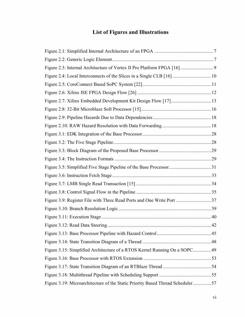
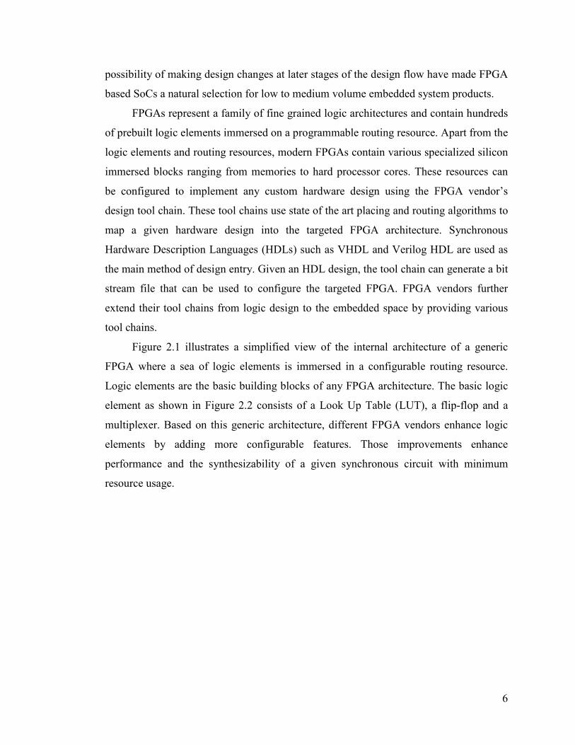
Figure 2.1 illustrates a simplified view of the internal architecture of a generic
FPGA where a sea of logic elements is immersed in a configurable routing resource.
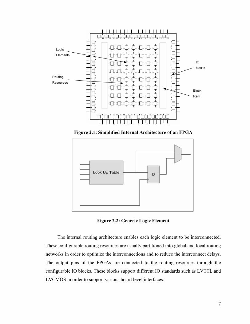
Logic elements are the basic building blocks of any FPGA architecture. The basic logic
element as shown in Figure 2.2 consists of a Look Up Table (LUT), a flip-flop and a
multiplexer. Based on this generic architecture, different FPGA vendors enhance logic
elements by adding more configurable features. Those improvements enhance
performance and the synthesizability of a given synchronous circuit with minimum
resource usage.
7
Figure 2.1: Simplified Internal Architecture of an FPGA
Figure 2.2: Generic Logic Element
The internal routing architecture enables each logic element to be interconnected.
These configurable routing resources are usually partitioned into global and local routing
networks in order to optimize the interconnections and to reduce the interconnect delays.
The output pins of the FPGAs are connected to the routing resources through the
configurable IO blocks. These blocks support different IO standards such as LVTTL and
LVCMOS in order to support various board level interfaces.
Block
Ram
IO
blocks
Logic
Elements
Routing
Resources
8
Routing lines are implemented using MOS transmission gates with SRAM bits
controlling the gates. The configurability of the logic elements as well as IO blocks are
implemented in a similar fashion using SRAM bits. These SRAM bits are called the
configuration memory of the FPGA. In order to implement a custom circuit, the
configuration memory of the FPGA needs to be programmed. Most of the FPGAs are
SRAM based and come with JTAG interface or a proprietary interface for the
configuration. The design tool chains provided by the vendor have support for FPGA
configuration using a special interface cable.
2.2 Platform FPGAs - Vertex II Pro
As the density of given technology grows, FPGA vendors tend to integrate
dedicated functional blocks into the logic fabric. For example, Xilinx Vertex [3] family
has hardcore PowerPC processors directly immersed in the logic fabric capable of
running at very high clock speeds. Apart from this hardcore processor trend, most FPGA
vendors integrate specialized IO processing blocks around the logic fabric including
physical MAC layers, high speed transceivers, etc. These types of FPGAs with
specialized silicon immersed IPs are known as platform FPGAs.
Vertex II Pro [16] is a platform FPGA that comes with two PowerPC processor
blocks, an array of memory blocks and multipliers immersed in the configurable logic
fabric. Vertex family FPGAs target high performance embedded systems and the
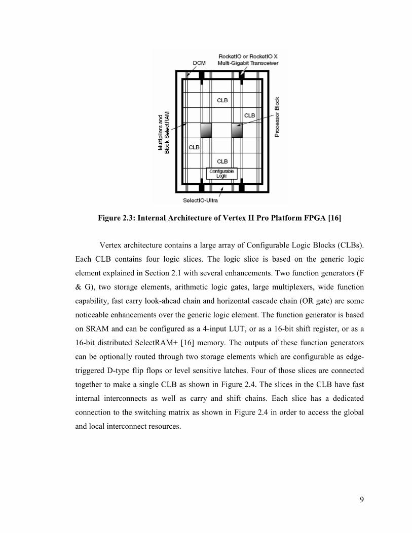
architecture is tailored specifically for the embedded domain. Figure 2.3 illustrates the
internal resources of the FPGA.
9
Figure 2.3: Internal Architecture of Vertex II Pro Platform FPGA [16]
Vertex architecture contains a large array of Configurable Logic Blocks (CLBs).
Each CLB contains four logic slices. The logic slice is based on the generic logic
element explained in Section 2.1 with several enhancements. Two function generators (F
& G), two storage elements, arithmetic logic gates, large multiplexers, wide function
capability, fast carry look-ahead chain and horizontal cascade chain (OR gate) are some
noticeable enhancements over the generic logic element. The function generator is based
on SRAM and can be configured as a 4-input LUT, or as a 16-bit shift register, or as a
16-bit distributed SelectRAM+ [16] memory. The outputs of these function generators
can be optionally routed through two storage elements which are configurable as edge-
triggered D-type flip flops or level sensitive latches. Four of those slices are connected
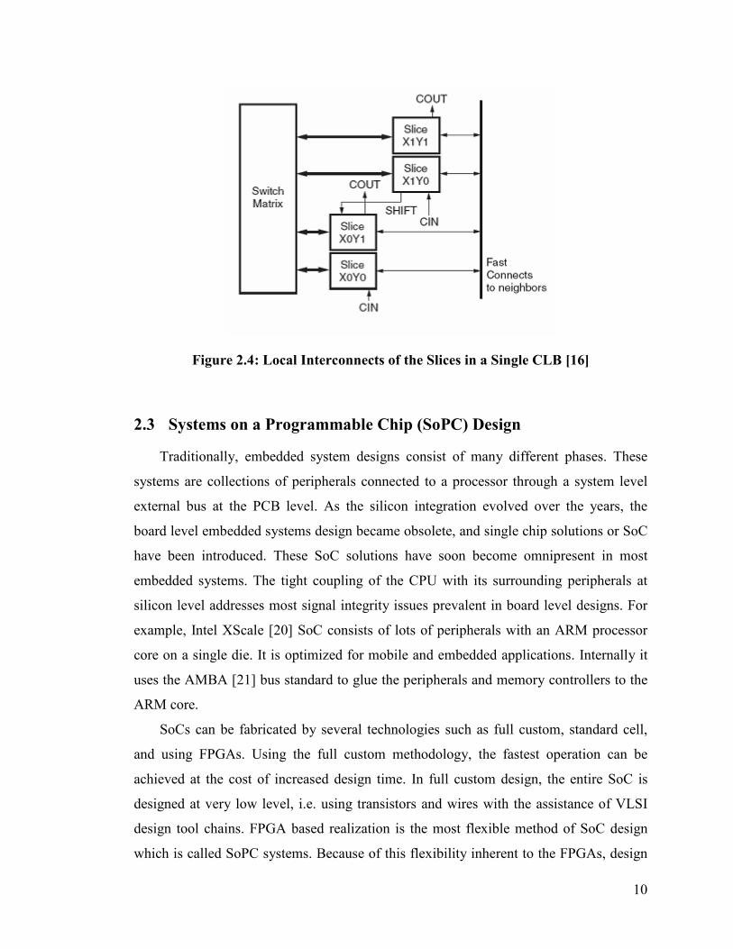
together to make a single CLB as shown in Figure 2.4. The slices in the CLB have fast
internal interconnects as well as carry and shift chains. Each slice has a dedicated
connection to the switching matrix as shown in Figure 2.4 in order to access the global
and local interconnect resources.
10
Figure 2.4: Local Interconnects of the Slices in a Single CLB [16]
2.3 Systems on a Programmable Chip (SoPC) Design
Traditionally, embedded system designs consist of many different phases. These
systems are collections of peripherals connected to a processor through a system level
external bus at the PCB level. As the silicon integration evolved over the years, the
board level embedded systems design became obsolete, and single chip solutions or SoC
have been introduced. These SoC solutions have soon become omnipresent in most
embedded systems. The tight coupling of the CPU with its surrounding peripherals at
silicon level addresses most signal integrity issues prevalent in board level designs. For
example, Intel XScale [20] SoC consists of lots of peripherals with an ARM processor
core on a single die. It is optimized for mobile and embedded applications. Internally it
uses the AMBA [21] bus standard to glue the peripherals and memory controllers to the
ARM core.
SoCs can be fabricated by several technologies such as full custom, standard cell,
and using FPGAs. Using the full custom methodology, the fastest operation can be
achieved at the cost of increased design time. In full custom design, the entire SoC is
designed at very low level, i.e. using transistors and wires with the assistance of VLSI
design tool chains. FPGA based realization is the most flexible method of SoC design
which is called SoPC systems. Because of this flexibility inherent to the FPGAs, design
11
errors can be easily corrected during the verification process. When it comes to standard
cell or full custom methods (ASIC based), correction of design faults has very high
prices, because the system is implemented directly on the silicon, which cannot be
altered.
When it comes to the SoPC systems, the internal bus architecture is one of the most
important aspects. There are several industry standard bus architectures including,
AMBA [21], IBM CoreConnect [22] and Wishbone [23]. Xilinx uses IBM’s
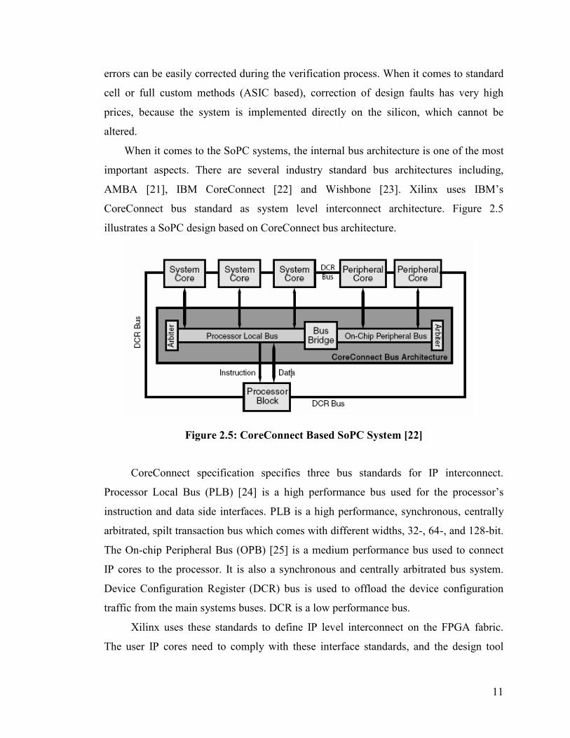
CoreConnect bus standard as system level interconnect architecture. Figure 2.5
illustrates a SoPC design based on CoreConnect bus architecture.
Figure 2.5: CoreConnect Based SoPC System [22]
CoreConnect specification specifies three bus standards for IP interconnect.
Processor Local Bus (PLB) [24] is a high performance bus used for the processor’s
instruction and data side interfaces. PLB is a high performance, synchronous, centrally
arbitrated, spilt transaction bus which comes with different widths, 32-, 64-, and 128-bit.
The On-chip Peripheral Bus (OPB) [25] is a medium performance bus used to connect
IP cores to the processor. It is also a synchronous and centrally arbitrated bus system.
Device Configuration Register (DCR) bus is used to offload the device configuration
traffic from the main systems buses. DCR is a low performance bus.
Xilinx uses these standards to define IP level interconnect on the FPGA fabric.
The user IP cores need to comply with these interface standards, and the design tool

12
chain comes with various IP cores for standard interfaces. These IPs include OPB
DRAM controllers, OPB RS232 IPs, OPB SPI IPs, etc.
The tool chain provided by the FPGA vendors greatly simplifies the FPGA design.
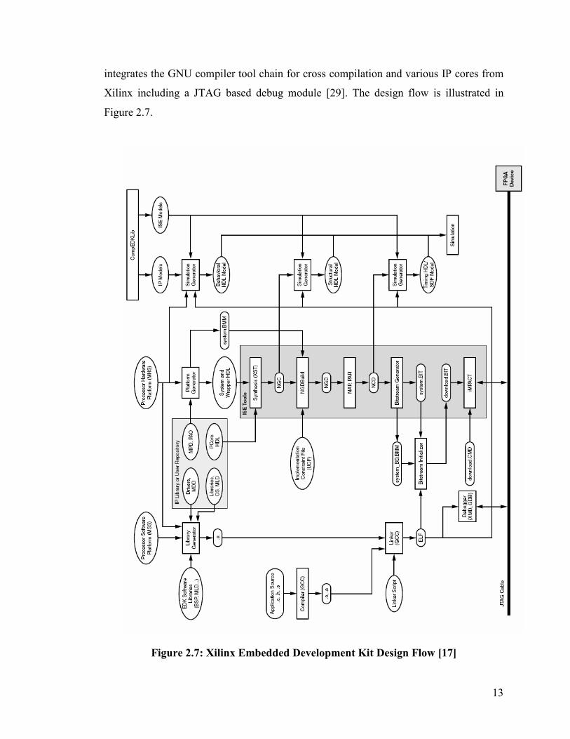
Xilinx Embedded Development Kit (EDK) [17] provides a graphical interface for high
level design of the embedded system while Xilinx Integrated Software Environment
(ISE) [26] provides the logic design and simulation environment.
The ISE is the synthesis engine which ultimately maps a given VHDL design to a
configuration bit stream for a targeted FPGA. Timing analysis is used at all possible
levels of design flow [27] in order to isolate the timing issues at the earliest possible
stage as shown in Figure 2.6.
Figure 2.6: Xilinx ISE FPGA Design Flow [26]
Ever increasing design complexity of embedded systems has resulted in a new
design philosophy; the codesign [28] of software and hardware. This allows one to
reduce the time to market window and accelerate the design process by concurrently
designing both hardware and software for the embedded system. Xilinx EDK is an
embedded system codesign environment that works on top of ISE. EDK is basically IP
interconnect and configuration utility which greatly simplifies the SoPC design. EDK
13
integrates the GNU compiler tool chain for cross compilation and various IP cores from
Xilinx including a JTAG based debug module [29]. The design flow is illustrated in
Figure 2.7.
Figure 2.7: Xilinx Embedded Development Kit Design Flow [17]
14
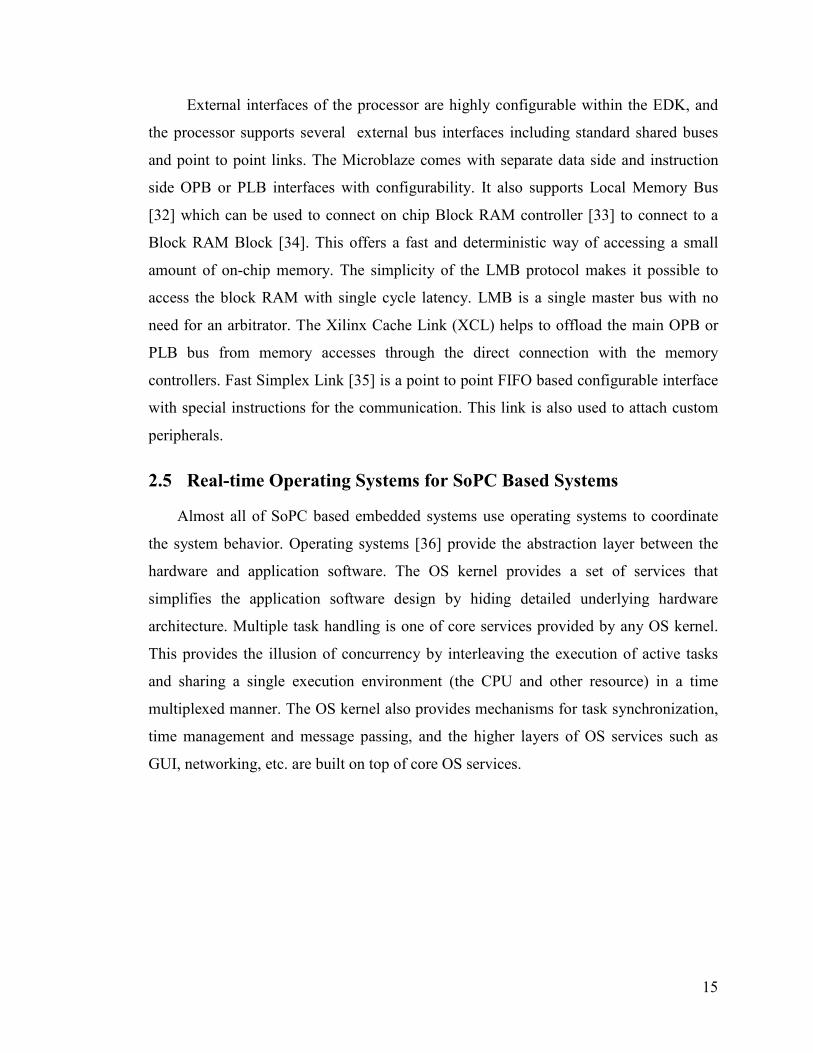
2.4 Configurable Softcore Processors for FPGAs
Most of the time SoPCs are built using softcore processors. A softcore processor is
an IP core fully described using an HDL which can be synthesized in an FPGA.
Configurability of a FPGA based SoPC is the most noticeable attractiveness over silicon
implemented SoCs. The configurability comes in two types [30, 31]. The dynamic
reconfigurablity allows one to reconfigure the full or a portion of the FPGA on the fly.
This concept is further extended to provide virtual hardware closely resembling the
concept of virtual memory systems used in modern CPUs. Static configurability is the
feature which allows the configuration of components at design time. For example, the
features of a soft core processor such as number of pipeline stages, use of hardware
multipliers, size of the cache memory, etc. can be configured at design time in order to
maximally align the architecture to the targeted application domain.
FPGA vendors also offer configurable softcore processor solutions which can be
tailored for the specific need of a particular embedded system. These softcore processors
are mainly targeted for their own FPGA architectures and optimized to utilize the
resources wisely while providing clock frequencies as high as 100MHz.
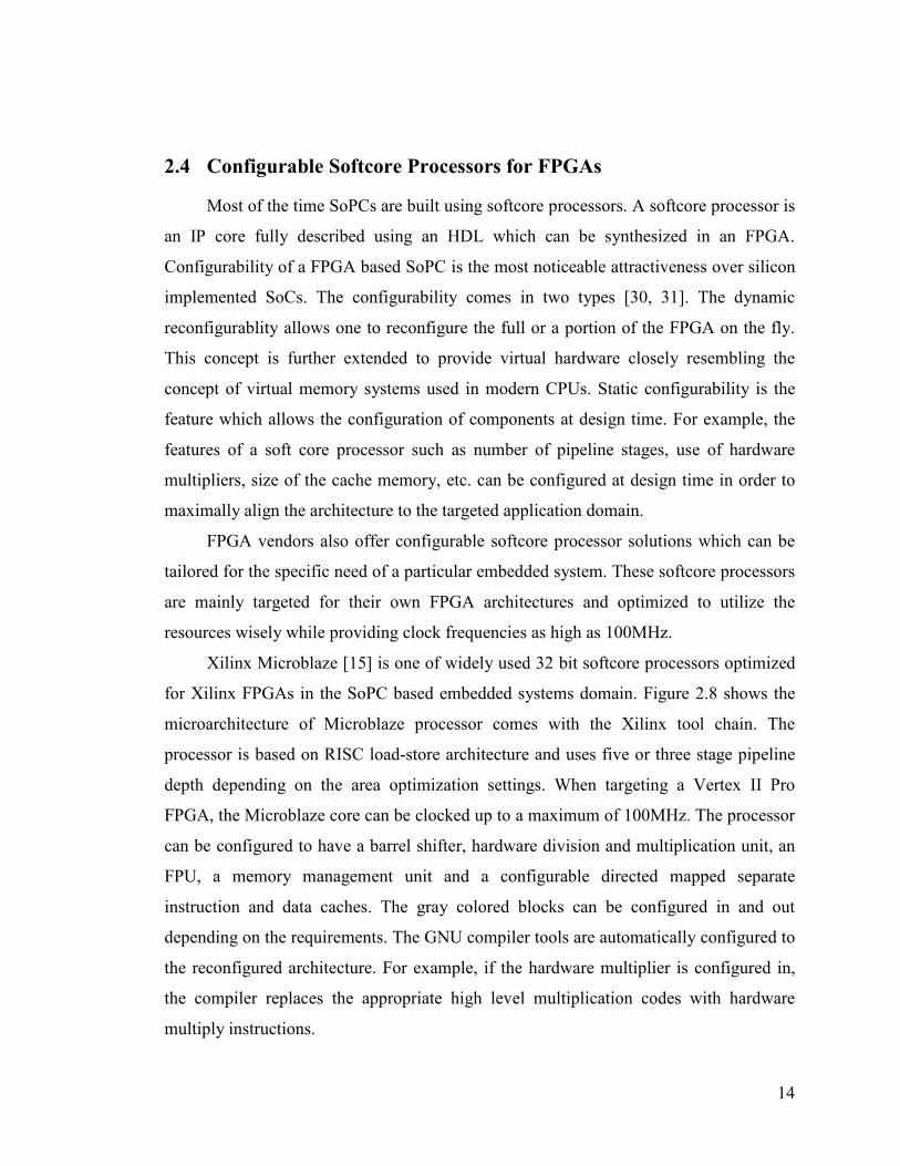
Xilinx Microblaze [15] is one of widely used 32 bit softcore processors optimized
for Xilinx FPGAs in the SoPC based embedded systems domain. Figure 2.8 shows the
microarchitecture of Microblaze processor comes with the Xilinx tool chain. The
processor is based on RISC load-store architecture and uses five or three stage pipeline
depth depending on the area optimization settings. When targeting a Vertex II Pro
FPGA, the Microblaze core can be clocked up to a maximum of 100MHz. The processor
can be configured to have a barrel shifter, hardware division and multiplication unit, an
FPU, a memory management unit and a configurable directed mapped separate
instruction and data caches. The gray colored blocks can be configured in and out
depending on the requirements. The GNU compiler tools are automatically configured to
the reconfigured architecture. For example, if the hardware multiplier is configured in,
the compiler replaces the appropriate high level multiplication codes with hardware
multiply instructions.
15
External interfaces of the processor are highly configurable within the EDK, and
the processor supports several external bus interfaces including standard shared buses
and point to point links. The Microblaze comes with separate data side and instruction
side OPB or PLB interfaces with configurability. It also supports Local Memory Bus
[32] which can be used to connect on chip Block RAM controller [33] to connect to a
Block RAM Block [34]. This offers a fast and deterministic way of accessing a small
amount of on-chip memory. The simplicity of the LMB protocol makes it possible to
access the block RAM with single cycle latency. LMB is a single master bus with no
need for an arbitrator. The Xilinx Cache Link (XCL) helps to offload the main OPB or
PLB bus from memory accesses through the direct connection with the memory
controllers. Fast Simplex Link [35] is a point to point FIFO based configurable interface
with special instructions for the communication. This link is also used to attach custom
peripherals.
2.5 Real-time Operating Systems for SoPC Based Systems
Almost all of SoPC based embedded systems use operating systems to coordinate
the system behavior. Operating systems [36] provide the abstraction layer between the
hardware and application software. The OS kernel provides a set of services that
simplifies the application software design by hiding detailed underlying hardware
architecture. Multiple task handling is one of core services provided by any OS kernel.
This provides the illusion of concurrency by interleaving the execution of active tasks
and sharing a single execution environment (the CPU and other resource) in a time
multiplexed manner. The OS kernel also provides mechanisms for task synchronization,
time management and message passing, and the higher layers of OS services such as
GUI, networking, etc. are built on top of core OS services.
16
Figure 2.8: 32-Bit Microblaze Soft Processor [15]
Operating systems are usually categorized as either general purpose or real-time.
The key differences between these two categorizations are the requirement of meeting
the given deadlines of tasks and the determinism of the behavior of the system. Real-
time systems are further categorized into soft real-time systems and hard real-time
systems. Hard real-time systems have strict deadlines and although a missed deadline
may even be catastrophic, this requirement is relaxed for the soft real-time systems. The
determinism is one of main design goals of any real-time operating system. Simply put,
given systems call needs to be serviced by the kernel within given time bounds. The
general purpose OSs do not stress on such requirements resulting in very
nondeterministic behavior, which is not an issue for the targeted application domains.
For the guaranteed meeting of deadlines and increased determinism, the real-time
operating systems are equipped with specialized scheduling algorithms [37]. The
scheduling algorithm needs to be selected depending on the application context of the
embedded system. For example, for the uniprocessor based hard real-time systems, the
Earliest Deadline First (EDF) algorithm is capable of finding the optimal feasible
schedule [38].
17
Xilkernal [39] is an open source small footprint robust software RTOS that comes
with the Xilinx EDK tool chain. Integration with EDK helps to create SoPC systems
running Xilkernal with little effort. Xilkernal provides a POSIX like interface with the
ability to handle semaphores, interrupts, mutexes and message queues. Modularity of the
kernel allows configurability of these modules. As a result, the kernel can be tailored for
the specific needs of the given application. Xilkernal supports both priority-based
preemptive scheduling and round robin scheduling. The policy is global and needs to be
initialized at configuration time of the kernel.
2.6 Multithreaded Processors
Almost all modern processors use the concept of pipelining [40] in order to
maximize the throughput of the processor. The pipelined execution divides each
instruction into subparts. This leads to the overlapped execution of consecutive
instructions. If two data dependant instructions are being executed in the pipeline, the
current instruction at the execution stage cannot obtain the latest value from the register
file since the earlier instruction is still at the later stages of the pipeline where the write
back of results occurs. This leads to a problem called data hazards, and this particular
type is known as Read After Write (RAW) hazards.
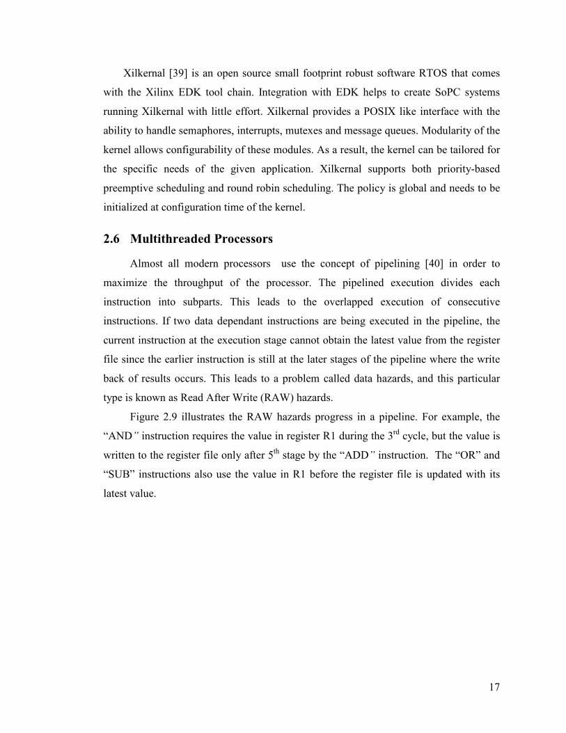
Figure 2.9 illustrates the RAW hazards progress in a pipeline. For example, the
“AND” instruction requires the value in register R1 during the 3rd cycle, but the value is
written to the register file only after 5th stage by the “ADD” instruction. The “OR” and
“SUB” instructions also use the value in R1 before the register file is updated with its
latest value.
18
Figure 2.9: Pipeline Hazards Due to Data Dependencies
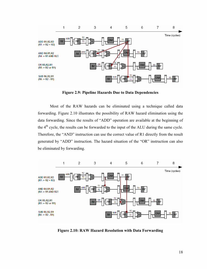
Most of the RAW hazards can be eliminated using a technique called data
forwarding. Figure 2.10 illustrates the possibility of RAW hazard elimination using the
data forwarding. Since the results of “ADD” operation are available at the beginning of
the 4th cycle, the results can be forwarded to the input of the ALU during the same cycle.
Therefore, the “AND” instruction can use the correct value of R1 directly from the result
generated by “ADD” instruction. The hazard situation of the “OR” instruction can also
be eliminated by forwarding.
Figure 2.10: RAW Hazard Resolution with Data Forwarding

19
Data forwarding is not always capable of resolving RAW hazards. For example,
if the “ADD” instruction was changed into a “LOAD” instruction to load R1 from the
data memory, the up-to-date value of R1 would be available only after the 4th cycle.
However, the “AND” instruction needs the value of R1 at the beginning of the 4th cycle.
Pipeline stall is required to overcome this hazard. This is done by freezing the first and
second stages during the 4th cycle and inserting a bubble into the 3rd stage.
Since the instructions are overlapped, the execution of branch instructions causes
another kind of hazards called control hazards. At the time a branch is resolved,
depending on the design of the pipeline, several instructions may be in progress. If the
branch is taken, all those instructions need to be flushed and pipeline has to be restarted
from the branch target address. Occasionally, branch delay slots are used to insert
independent instructions where those instructions always get executed irrespective of the
outcome of the branch instruction. The technique of branch prediction is used to
overcome the penalty due to control hazards by predicting the outcome of the branch and
to prefetch the target address in advance.
Multithreading [10] is another technique used to remove these penalties by
interleaving instructions from different threads without adding much complexity to the
processor pipeline. This technique does not improve the Cycles Per Instruction (CPI) of
the processor, but exploits the parallelism among threads. Multithreading comes in cycle
interleaved and block interleaved forms. Cycle interleaved multithreading [10]
eliminates both branch penalty and pipeline hazards by interleaving instructions from
different threads in every cycle. Multithreading is an attractive option to reduce the
pipeline hazards, but it does not increase the performance of a single threaded execution.
Block multithreading [10] is the coarse grained version of the cycle interleaved
multithreading where each thread is scheduled to run several cycles before switching to
another thread. Threads are switched on events like cache misses and taken branches, so
the processor can exploit the parallelism among the threads and can do useful work
while the cache line is being fetched. This technique can be used to hide the memory
latency in real-time systems [41]. Unlike the cycle interleaved case, all the forwarding
logic and hazard detection need to be implemented, since each thread needs to have the
possibility of running exclusively in the pipeline without being interrupted.
20
Multithreading is implemented by providing architectural extensions to the
pipeline to handle multiple threads at the hardware level. Conversion from a single
threaded processor to a multithreaded processor is fairly simple. The instruction fetch
stage should contain multiple program counters and a mechanism for switching the
threads. The decode stage needs to have a duplicated register file, where a separate
register is set for each thread. This duplication demands a larger register file. However,
the requirement of duplicated register file can be relaxed at the cost of increased context
switching time by using external tightly coupled context memory. Apart from the
duplicated register file, the multithreaded processors pipeline needs to carry thread IDs
to distinguish how the instructions belong to different threads. Since multithreaded
processor can have instructions from different threads in its pipeline, the thread IDs
needs to be propagated down the pipeline in order to associate each instruction with the
relevant thread.
2.7 Hardware Support for Operating Systems
Several independent research groups have focused on the hardware implementation
of the RTOS to take advantage of parallelism inherent to the hardware. The first OS
implementations in hardware date back to 1995. This section investigates the previous
research which mostly address on the separate, chip based migration of software RTOSs
into hardware.
The Real Time Unit (RTU) [1] implements complete RTOS functionality on an
Application Specific Integrated Circuit (ASIC). This chip works in parallel with the CPU
and sits on the processor bus and communicates through a set of memory mapped
registers. The main interrupt line of the processor is driven by this chip whenever a task
switch is required. Upon interruption, the CPU reads the NEXT TASK ID register of the
RTU and performs a context switch to run the newly selected process. The context
switching is done in software by saving and loading the registers in the task control
blocks. In this manner the CPU is offloaded from the kernel timer tick handling and the
process scheduling. Therefore, the processor cycles consumed on these can be
effectively used. This RTU uses static priority preemptive scheduling and supports up to
128 tasks with 8 priority levels. This RTU handles interrupts, periodic start of tasks,
21
delay tasks and activation and deactivation of tasks by itself. FASTCHAT [9] project
mates the above mentioned RTU with special CPU where it can perform the context
switching in one cycle. This is a very simple single cycle non-pipelined CPU with two
copies of the register file and other system and status registers. One set is used by the
CPU while the other set is used by the RTU. Once the RTU comes to the decision of
switching the task, it propagates its register file with the saved values in the Task
Control Block (TCB) corresponding to the new task to be run and interrupts the CPU.
Once interrupted, the CPU can immediately start executing the new task by switching to
the register set field by RTU. RTU94 [42] further extends the concept into the
multiprocessor domain by adding support to schedule processes in a multiprocessor
system. The real-time unit still sits on the shared bus, and each CPU has access to a
dedicated task register resides in the RTU. Unlike a single processor system, the policy
selection for the shared bus arbitration has a direct impact on the predictability of the
RTU calls. The only option is to use the round robin bus arbitration in order to be able to
calculate a maximum access time for the RTU. The nonpredictability of the RTU calls
increases further for the systems which employ bus locking mechanisms to provide
atomic transactions. When it comes to advanced bus based systems, where the dynamic
priority based arbitration is the natural selection, it is not possible to find a maximum
bound in order to characterize the timing model of the RTU, resulting in
nondeterminism. The RTU has been evolved further into a commercial product in the
form of an intellectual property named Sierra [43] by RealFast AB. This IP comes as an
IP addition [44] for the EDK.
The silicon TRON project [2] implements an RTOS in hardware by offloading
primitive OS functions from the CPU. Even though this one is conceptually equivalent
with the RTU, it has a thin software layer to meet the specifications of the ITRON
project.
The Spring Scheduling Co-Processor (SSCoP) [3] is a noticeable deviation of
hardware based realization of real-time kernels. This coprocessor accelerates the
scheduling algorithm used by the Spring distributed real-time computing system [45]. In
the context of single processor systems with preemptable tasks, the EDF and Least
Laxity First (LLF) algorithms are optimal dynamic scheduling algorithms. That is, if
22
those algorithms can’t find a feasible schedule no other algorithms can find a schedule.
But when it comes to the multiprocessor systems no optimal algorithms exist. In order to
find a full feasible scheduling in a multiprocessor system a heuristics based approach
needs to be used. SSCoP realizes a dynamic planning based scheduling algorithm with a
heuristic scheduling approach. It also supports static scheduling and different policies
including EDF. The schedule is made online as the tasks arrive, and if feasible
scheduling is found the newly arrived task is accepted. The SSCoP is implemented in
VLSI and has an asynchronous PROM interface in order to simplify the system
interface. Communication is done through polling the memory interface making the
interfacing inefficient and nondeterministic.
Similar to the SSCoP, Real Time Manager (RTM) [4] provides hardware support for
real-time operating systems which lies in the middle of pure hardware based solutions
and the pure software based solutions. The RTM provides a hardware based solution for
task management, time management and event management. RTM provides a generic
interface to the software and it can be easily integrated with existing RTOSs. RTM is
also a memory mapped peripheral and can be accessed to get the secluded task to be run.
The configurable hardware scheduler [8] is also a memory mapped IP based
solution proposed to offload the kernel overhead from the CPU. The main exception is,
the IP is targeted for the configurable space, and it can be configured to use the
following three scheduling algorithms: priority, earliest deadline first and rate monotonic
algorithms. The IP core comes with a configuration utility that allows the number of
tasks, number of external interrupts and timer resolution to be configured. The scheduler
is implemented using two priority queues. The base architecture remains the same for
each scheduling policy configured, but the sorting of the elements is done according to
the queue element fields depending on the scheduling policy being used.
Some research groups [5, 6] have focused on migrating only the scheduler
component of the kernel into hardware. Their main focus is to implement efficient and
complex scheduling algorithms in hardware, which otherwise is very inefficient with a
pure software based approach. Saez, et al. [6], proposes a hardware implementation to
address the issue of impractical software implementation of the slack stealing algorithm
23
which is efficient for jointly scheduling both hard deadline periodic tasks and soft
aperiodic tasks.
Partitioning between implementation in hardware and implementation in software of
the real-time kernels has also been investigated by several research groups in order to
analyze the possible speedup while using minimal hardware resources. The SoC/RTOS
codesign framework [46] allows the designer to selectively migrate Atalanta [47] kernel
components into hardware. This fine grained partitioning helps to achieve significant
speedup with minimum hardware resources. A hardware/software kernel for SoC design
[48] proposes an efficient way to partition the EDF scheduler into software and hardware
implementations. This research further evaluates various options for software/hardware
partitioning.
Previous research work proves that the hardware migration of partial or full kernel
improves the overall performance of the RTOS. Apart from the commercialization
efforts such as RealFast [43], which is fairly successful, current commercial RTOS are
fully based on software implementations. Several factors contribute to this
unattractiveness of the hardware based solution, since most research work is focused on
silicon implementations. Historically all these implementations are based on dedicated
silicon, residing external to the CPU and number of tasks supported by the hardware
RTOS is fixed.
2.8 Processors with OS Level Support
The research work described earlier focused on the hardware migration of RTOS
to remove the OS overhead and mainly focused on scheduler migration. The context
switching overhead also contributes to a significant amount of OS overhead. Every time
the OS performs a context switch, the CPU’s architectural registers need to be saved and
the new states related to the context being restored have to be loaded. In order to remove
this overhead, the special processor has to be used. This section investigates processors
with OS level support, including efficient context switching and interrupt handling.
When it comes to the domain of general purpose processors, some of those
processors have special support for the efficient context switching including IA 32 [49]
based processors. The Task State Segments (TSS) stores all the state information related
24
to each task, and the processor performs the restoration transparently and efficiently.
Apart from these types of supports, most general purpose processors do not provide
considerable OS level support for efficient context switching.
The Transputer [50] has the ability to handle multiple concurrent tasks. It is the
first known processor implementation with OS level support in a very limited fashion.
Transputer implements a round robin scheduler for task scheduling, timer queues and
some special instructions to make the thread sleep for a specified time. It uses the
technique of windowing registers to implement fast context switches. Software Defined
Silicon [51] is a new multiprocessor architecture stemmed from the Transputer
architecture.
Several research works have been done to exploit excellent context switching
characteristics of multithreading processors in the domain of real time systems. The first
method is to use the fast context switching characteristic to hide the memory access
latency in real time systems [41]. The second method is to use fast context switching
ability to implement responsive interrupt service threads, which are directly executed
upon the event of an external interrupt. Komodo [11] is a 4-way multithreaded processor
with a hardware supported event handling mechanism based on hardware interrupt
service threads. This processor lies between cycle interleaved multithreading and block
interleaved multithreading. The processor supports four hardware threads with
duplicated register files which can be used as Interrupt Service Threads (IST). The
instruction fetch stage of Komodo is feasible for implementing several scheduling
schemes. When it comes to the handling of multiple hard real-time events
simultaneously, the guaranteed percentage scheduling scheme outperforms the optimal
EDF algorithm by guaranteeing not only that the deadline is met but also the sustained
data rates by interleaving the active threads. The zero context switching overhead helps
achieve this by implementing a very fine grained implementation of the guaranteed
percentage scheduling algorithm. The Komodo project has been further extended to
implement a Java based microcontroller [12-14] targeting real-time applications. Three
hardware threads are used for real-time threads, and the remaining one is shared among
non real-time threads.
25
Jackknife [52] is an AVR compatible multithreaded processor supporting 8
hardware threads. This processor also implements the ISTs with hardware support. The
instruction fetch stage implements a round robin scheduler to interleave the active
threads and interrupts are serviced in next cycle. Jackknife supports a synchronization
mechanism using an external memory mapped peripheral.
The PRESTOR-1 [53] implements a virtual number of hardware contexts using a
special context swapping architecture. Based on the virtual context architecture of the
PRESTOR, a RTOS kernel [54] based on ITRON is proposed. This processor uses cache
memory with priority based partitioning and provides support for fast interrupt
processing using the multiple context support.
Java language itself has support for multithreading. The JVM maps those software
threads to the OS threads depending on the JVM implementation. Significant research
has been done in the area of hardware implementation of JVM. Java Optimized
Processor (JOP) [55] is a processor that executes JAVA byte code at the hardware level.
Several commercialized architectures such as ARM, provides hardware level JVM
implementations in order to accelerate java byte code execution. However, hardware
implementation of Java virtual machine causes considerable overhead and is not suitable
for hard real-time systems.
26
Chapter 3
Design and Implementation of the
RTBlaze
This thesis combines the earlier research work on both hardware realizations of
RTOSs and multithreaded processors to design a new processor, RTBlaze, with tightly
coupled hardware RTOS. RTBlaze is a multithreaded processor that integrates a static
priority based preemptive scheduler, timer and semaphore handling queues to the
pipeline.
The first part of this chapter describes the design of the base processor compatible
with MicroBlaze. The second part of this chapter discusses the architectural
modifications made to the base processor in order to augment the instruction set with
RTOS level support.
27
3.1 Design of the Base Processor
Due to the availability of the EDA tool chain for SoPC design and the GNU
compiler tool chain from Xilinx, the base processor is designed to be an instruction set
compatible with basic MicroBlaze. This compatibility enables seamless integration of
the base processor with the Xilinx tool chain and reusability of library IP cores with the
existing device drivers. To be compatible, the base processor needs to do the following.
• Implement the bus standards supported by MicroBlaze
• Be compatible MicroBlaze Instruction set
• Be cycle accurate with MicroBlaze
Since the base processor implementation is targeted for the demonstration of the
hardware RTOS concept, a minimalist implementation of the base processor is carried
out with following components.
• A 32 x 32 bit register file
• A special purpose registers
• An ALU
• An instruction side LMB memory interface
• A data side LMB memory interface
Thus, exception handling, PLB interface, Fast Simplex Links, and the configurable parts
of the MicroBlaze are not implemented.
The processor features a 32 bit address bus with memory mapped IO. Even though
the processor uses Harvard architecture with split instruction and data memory
interfaces, the EDK overlaps both address space by mapping both interfaces to the same
memory block through LMB to Block RAM controller IP as shown in Figure 3.1. Apart
from the memory controllers, other custom peripherals can be connected to the LMB bus
within the EDK.

28
Figure 3.1: EDK Integration of the Base Processor
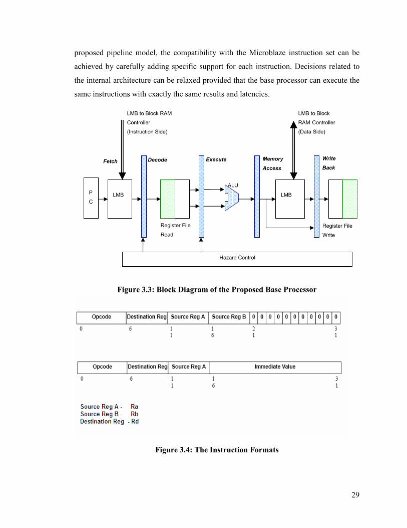
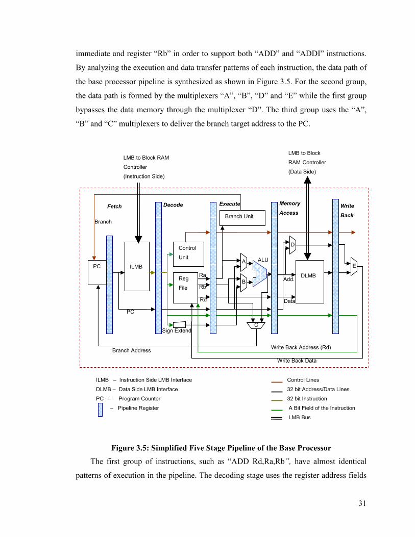
Figure 3.2: The Five Stage Pipeline
The base processor implements minimalist MicroBlaze instruction set using a
five stage pipeline as shown in Figure 3.2. Figure 3.3 shows the simplified pipeline
schematic of the base processor. The fetch stage retrieves the 32-bit fixed size, word
aligned instruction from instruction side LMB. The Program Counter (PC) is also
updated to point to the next instruction during this stage. The decoding stage performs
the instruction decoding and control signal generation. The register file is also addressed
with corresponding register address fields of the instruction. Execution stage performs
the operation specified in the opcode of the instruction using the ALU. Memory stage
performs data read and write operations with the support for different data widths
through the data side LMB bus connected to on chip block RAM. The write back stage
writes the result into the register file. The pipeline carries the data path signals as well as
control signals to each stage. The hazard detection and control unit performs the freezing
and flushing of the pipeline depending on the hazard situation in progress. Based on the
Fetch Decode Execute Mem. Access Write back
Fetch Decode Execute Mem. Access
Fetch Decode Execute
Fetch Decode
Fetch
Base Processor
Block
RAM
Wrapper
LMB to Block
RAM Controller
LMB to Block
RAM Controller
Data Side
LMB
Interface
Instruction
Side LMB
Interface
Instruction/Data
Memory
29
proposed pipeline model, the compatibility with the Microblaze instruction set can be
achieved by carefully adding specific support for each instruction. Decisions related to
the internal architecture can be relaxed provided that the base processor can execute the
same instructions with exactly the same results and latencies.
Figure 3.3: Block Diagram of the Proposed Base Processor
Figure 3.4: The Instruction Formats
Fetch
LMB
LMB
Hazard Control
Decode Execute Memory
Access
Write
Back
LMB to Block RAM Controller
(Instruction Side)
LMB to Block
RAM Controller
(Data Side)
P
C
Register File
Read
Register File
Write
ALU
30
Table 3.1: A Partial List of Microblaze Instruction Set
Group Instruction Semantics
ADD Rd,Ra,Rb Rd := Rb + Ra
ADDI Rd,Ra,Imm Rd := s(Imm) + Ra
RSUB Rd,Ra,Rb Rd := Rb + Ra + 1
Arithmetic, Logical and
Shifting instructions
OR Rd,Ra,Rb Rd := Ra or Rb
LW Rd,Ra,Rb Addr := Ra + Rb
Rd := *Addr Load/Store instructions
SW Rd,Ra,Rb
Addr := Ra + Rb
*Addr := Rd
BRLD Rd,Rb PC := PC + Rb
Rd := PC
BRA Rb PC := Rb
BEQ Ra,Rb PC := PC + Rb if Ra = 0
RTSD Ra,Imm PC := Ra + s(Imm)
BRAI Imm PC := s(Imm)
Control transfer
instructions
BEQI Ra,Imm PC := PC + s(Imm) if Ra = 0
The MicroBlaze instructions have two main formats as shown in Figure 3.4. All
MicroBlaze instructions are defined as either Type A or Type B [15]. Type A
instructions have up to two source register operands and one destination register
operand. Type B instructions have one source register and a 16-bit immediate operand.
Sign extension is used to extend the 16 bit immediate operand of the instruction into a 32
bit word by preserving the sign of the immediate value. Type B instructions have a
single destination register operand. Based on the execution patterns in the pipeline, the
instruction set of Microblaze can be categorized into following groups.
1. Arithmetic, Logical and Shifting instructions
2. Load/Store instructions
3. Control transfer instructions
The Microblaze instruction set contains more than 100 instructions. A partial list of
instructions in each group is shown in Table 3.1. In order to support the execution of
those instructions, the data transfer paths in the pipeline need to be multiplexed. For
example, one input of the ALU needs to be multiplexed between the sign extended
31
immediate and register “Rb” in order to support both “ADD” and “ADDI” instructions.
By analyzing the execution and data transfer patterns of each instruction, the data path of
the base processor pipeline is synthesized as shown in Figure 3.5. For the second group,
the data path is formed by the multiplexers “A”, “B”, “D” and “E” while the first group
bypasses the data memory through the multiplexer “D”. The third group uses the “A”,
“B” and “C” multiplexers to deliver the branch target address to the PC.
Figure 3.5: Simplified Five Stage Pipeline of the Base Processor
The first group of instructions, such as “ADD Rd,Ra,Rb”, have almost identical
patterns of execution in the pipeline. The decoding stage uses the register address fields
Control Lines
32 bit Address/Data Lines
32 bit Instruction
A Bit Field of the Instruction
LMB Bus
ILMB – Instruction Side LMB Interface
DLMB – Data Side LMB Interface
PC – Program Counter
– Pipeline Register
DLMB Reg
File
ILMB
Control
Unit
PC
ALU
Branch Unit
LMB to Block RAM Controller
(Instruction Side)
PC
Write Back Address (Rd)
LMB to Block
RAM Controller
(Data Side)
Write Back Data
Branch Address
Decode Execute Fetch Memory
Access
Ra
Rb
Rd
Branch
Write
Back
Data
Add.
Sign Extend
A
B
C
D
E
32
of the instruction to address the register file. The register values are forwarded to the
execution stage in next cycle. The sign-extended value of the immediate field of the
instruction is also forwarded to the execution stage. During the execution stage, the ALU
is provided with relevant input values, and the operation is selected using the control
signals present at the execution stage. In the memory access stage, the result is directly
forwarded to the writeback stage, since this type of instruction does not perform any data
memory access. The writeback stage accesses the register file to write the value to the
destination register.
The load/store instructions access data memory using register indirect addressing.
These instructions have three arguments, two source register fields and one
source/destination register field. Both source operands are used to calculate the address
of the memory location being accessed using the ALU. For the store instructions, the
value in the destination register is written to memory during the memory access stage.
The destination register is used to store the value read from the memory for the load
instructions.
Control transfer instructions modify the program counter depending on a given
condition. During the decoding stage, the register file is accessed to retrieve the values
related to the condition evaluation. The condition is evaluated during the execution stage
using special comparators. The ALU calculates the address of the branch target. If the
condition is resolved to true, the program counter in the fetch stage is loaded with the
newly calculated address.
The following sections provide a detailed architectural description of the base
processor design.
33
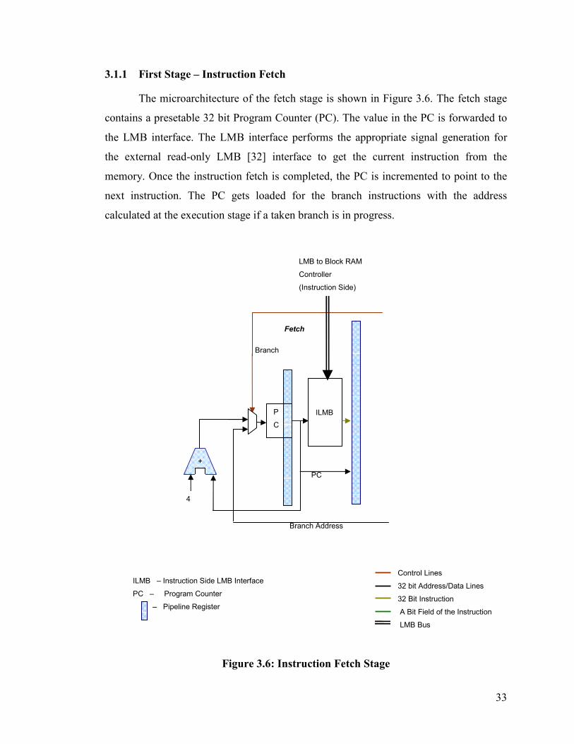
3.1.1 First Stage – Instruction Fetch
The microarchitecture of the fetch stage is shown in Figure 3.6. The fetch stage
contains a presetable 32 bit Program Counter (PC). The value in the PC is forwarded to
the LMB interface. The LMB interface performs the appropriate signal generation for
the external read-only LMB [32] interface to get the current instruction from the
memory. Once the instruction fetch is completed, the PC is incremented to point to the
next instruction. The PC gets loaded for the branch instructions with the address
calculated at the execution stage if a taken branch is in progress.
Figure 3.6: Instruction Fetch Stage
Control Lines
32 bit Address/Data Lines
32 Bit Instruction
A Bit Field of the Instruction
LMB Bus
ILMB P
C
LMB to Block RAM Controller
(Instruction Side)
PC
Branch Address
Fetch
Branch
+
4
ILMB – Instruction Side LMB Interface
PC – Program Counter
– Pipeline Register
34
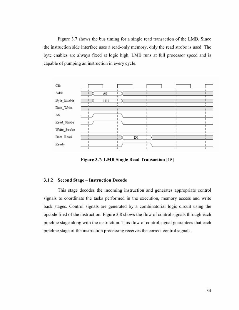
Figure 3.7 shows the bus timing for a single read transaction of the LMB. Since
the instruction side interface uses a read-only memory, only the read strobe is used. The
byte enables are always fixed at logic high. LMB runs at full processor speed and is
capable of pumping an instruction in every cycle.
Figure 3.7: LMB Single Read Transaction [15]
3.1.2 Second Stage – Instruction Decode
This stage decodes the incoming instruction and generates appropriate control
signals to coordinate the tasks performed in the execution, memory access and write
back stages. Control signals are generated by a combinatorial logic circuit using the
opcode filed of the instruction. Figure 3.8 shows the flow of control signals through each
pipeline stage along with the instruction. This flow of control signal guarantees that each
pipeline stage of the instruction processing receives the correct control signals.
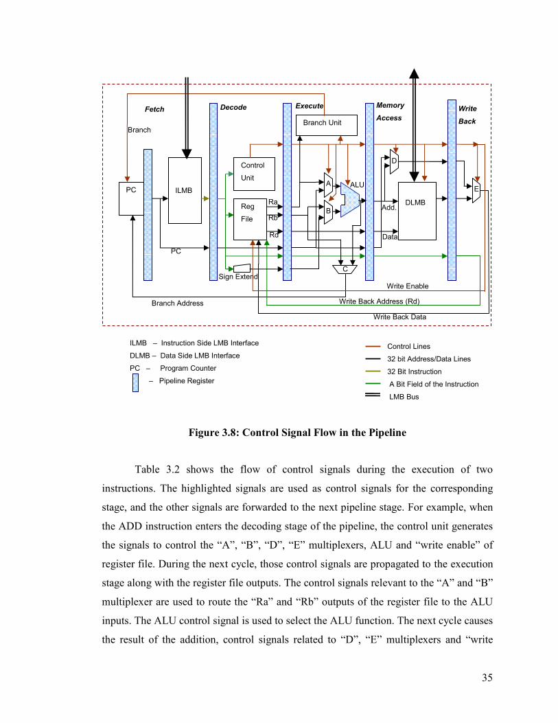
35
Figure 3.8: Control Signal Flow in the Pipeline
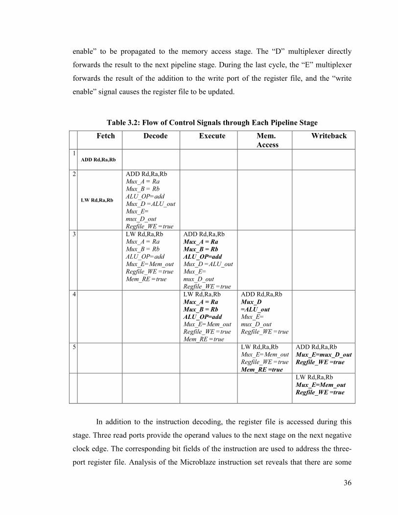
Table 3.2 shows the flow of control signals during the execution of two
instructions. The highlighted signals are used as control signals for the corresponding
stage, and the other signals are forwarded to the next pipeline stage. For example, when
the ADD instruction enters the decoding stage of the pipeline, the control unit generates
the signals to control the “A”, “B”, “D”, “E” multiplexers, ALU and “write enable” of
register file. During the next cycle, those control signals are propagated to the execution
stage along with the register file outputs. The control signals relevant to the “A” and “B”
multiplexer are used to route the “Ra” and “Rb” outputs of the register file to the ALU
inputs. The ALU control signal is used to select the ALU function. The next cycle causes
the result of the addition, control signals related to “D”, “E” multiplexers and “write
Sign Extend
Control Lines
32 bit Address/Data Lines
32 Bit Instruction
A Bit Field of the Instruction
LMB Bus
ILMB – Instruction Side LMB Interface
DLMB – Data Side LMB Interface
PC – Program Counter
– Pipeline Register
DLMB Reg
File
ILMB
Control
Unit
PC ALU
Branch Unit
PC
Write Back Address (Rd)
Write Back Data
Branch Address
Decode Execute Fetch Memory
Access
Ra
Rb
Rd
Branch
Write
Back
Data
Add.
A
B
C
D
E
Write Enable
36
enable” to be propagated to the memory access stage. The “D” multiplexer directly
forwards the result to the next pipeline stage. During the last cycle, the “E” multiplexer
forwards the result of the addition to the write port of the register file, and the “write
enable” signal causes the register file to be updated.
Table 3.2: Flow of Control Signals through Each Pipeline Stage
Fetch Decode Execute Mem.
Access
Writeback
1 ADD Rd,Ra,Rb
2
LW Rd,Ra,Rb
ADD Rd,Ra,Rb Mux_A = Ra
Mux_B = Rb
ALU_OP=add
Mux_D =ALU_out
Mux_E=
mux_D_out
Regfile_WE =true
3 LW Rd,Ra,Rb Mux_A = Ra
Mux_B = Rb
ALU_OP=add
Mux_E=Mem_out
Regfile_WE =true
Mem_RE =true
ADD Rd,Ra,Rb Mux_A = Ra
Mux_B = Rb
ALU_OP=add
Mux_D =ALU_out
Mux_E=
mux_D_out
Regfile_WE =true
4 LW Rd,Ra,Rb Mux_A = Ra
Mux_B = Rb
ALU_OP=add
Mux_E=Mem_out
Regfile_WE =true
Mem_RE =true
ADD Rd,Ra,Rb Mux_D
=ALU_out
Mux_E=
mux_D_out
Regfile_WE =true
5 LW Rd,Ra,Rb Mux_E=Mem_out
Regfile_WE =true
Mem_RE =true
ADD Rd,Ra,Rb Mux_E=mux_D_out
Regfile_WE =true
LW Rd,Ra,Rb Mux_E=Mem_out
Regfile_WE =true
In addition to the instruction decoding, the register file is accessed during this
stage. Three read ports provide the operand values to the next stage on the next negative
clock edge. The corresponding bit fields of the instruction are used to address the three-
port register file. Analysis of the Microblaze instruction set reveals that there are some
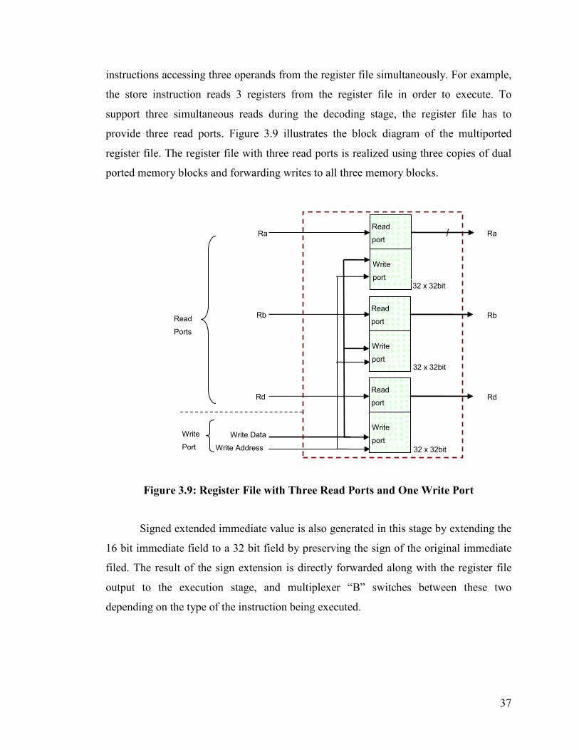
37
instructions accessing three operands from the register file simultaneously. For example,
the store instruction reads 3 registers from the register file in order to execute. To
support three simultaneous reads during the decoding stage, the register file has to
provide three read ports. Figure 3.9 illustrates the block diagram of the multiported
register file. The register file with three read ports is realized using three copies of dual
ported memory blocks and forwarding writes to all three memory blocks.
Figure 3.9: Register File with Three Read Ports and One Write Port
Signed extended immediate value is also generated in this stage by extending the
16 bit immediate field to a 32 bit field by preserving the sign of the original immediate
filed. The result of the sign extension is directly forwarded along with the register file
output to the execution stage, and multiplexer “B” switches between these two
depending on the type of the instruction being executed.
Read
port
Write
port
Read
port
Write
port
Read
port
Write
port
32 x 32bit
32 x 32bit
32 x 32bit
Ra
Rb
Rd
Ra
Rb
Rd
Write Data
Write Address
Read
Ports
Write
Port
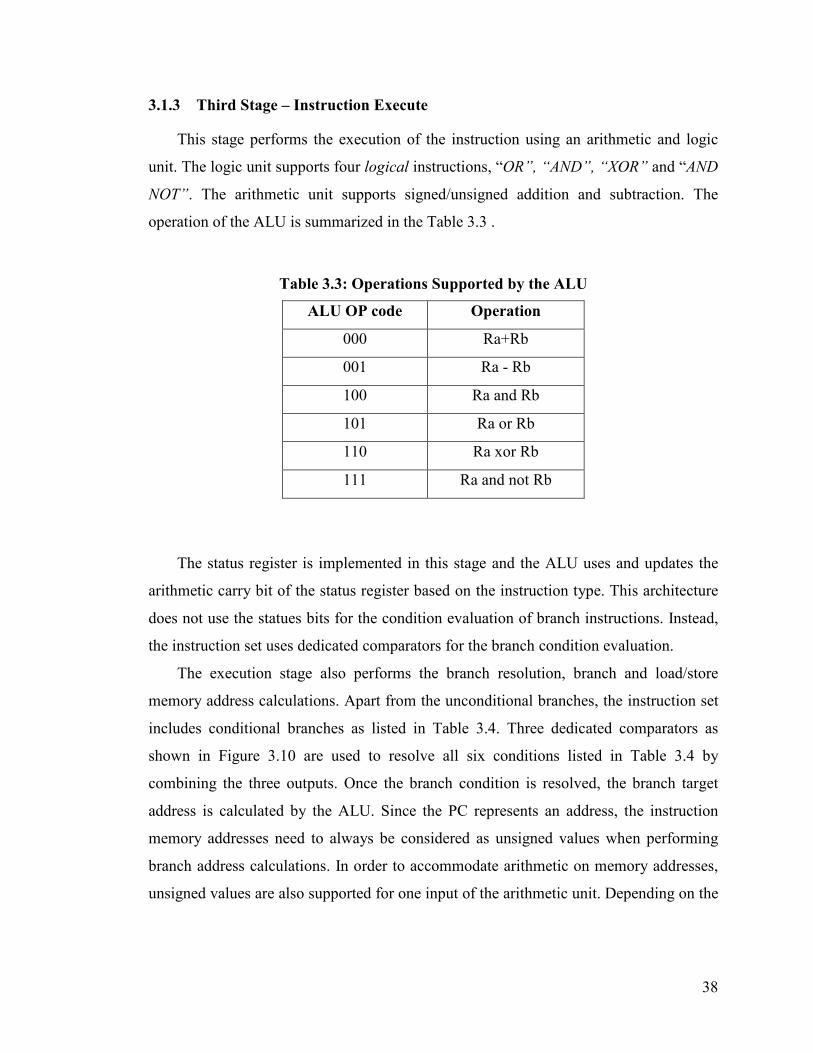
38
3.1.3 Third Stage – Instruction Execute
This stage performs the execution of the instruction using an arithmetic and logic
unit. The logic unit supports four logical instructions, “OR”, “AND”, “XOR” and “AND
NOT”. The arithmetic unit supports signed/unsigned addition and subtraction. The
operation of the ALU is summarized in the Table 3.3 .
Table 3.3: Operations Supported by the ALU
ALU OP code Operation
000 Ra+Rb
001 Ra - Rb
100 Ra and Rb
101 Ra or Rb
110 Ra xor Rb
111 Ra and not Rb
The status register is implemented in this stage and the ALU uses and updates the
arithmetic carry bit of the status register based on the instruction type. This architecture
does not use the statues bits for the condition evaluation of branch instructions. Instead,
the instruction set uses dedicated comparators for the branch condition evaluation.
The execution stage also performs the branch resolution, branch and load/store
memory address calculations. Apart from the unconditional branches, the instruction set
includes conditional branches as listed in Table 3.4. Three dedicated comparators as
shown in Figure 3.10 are used to resolve all six conditions listed in Table 3.4 by
combining the three outputs. Once the branch condition is resolved, the branch target
address is calculated by the ALU. Since the PC represents an address, the instruction
memory addresses need to always be considered as unsigned values when performing
branch address calculations. In order to accommodate arithmetic on memory addresses,
unsigned values are also supported for one input of the arithmetic unit. Depending on the

39
branch type, the calculated branch target value flows through multiplexer “C” to the
fetch stage as shown in Figure 3.11.
Table 3.4: Conditional Control Transfer Instructions
Figure 3.10: Branch Resolution Logic
Instruction Semantics
BEQ Ra,Rb PC := PC + Rb if Ra = 0
BNE Ra,Rb PC := PC + Rb if Ra != 0
BLT Ra,Rb PC := PC + Rb if Ra < 0
BLE Ra,Rb PC := PC + Rb if Ra <= 0
BGT Ra,Rb PC := PC + Rb if Ra > 0
BGE Ra,Rb PC := PC + Rb if Ra >= 0
= 0
>0
<0
Combinatorial
Logic Ra
Ra = 0 Ra! = 0 Ra < 0 Ra <= 0 Ra > 0 Ra >= 0
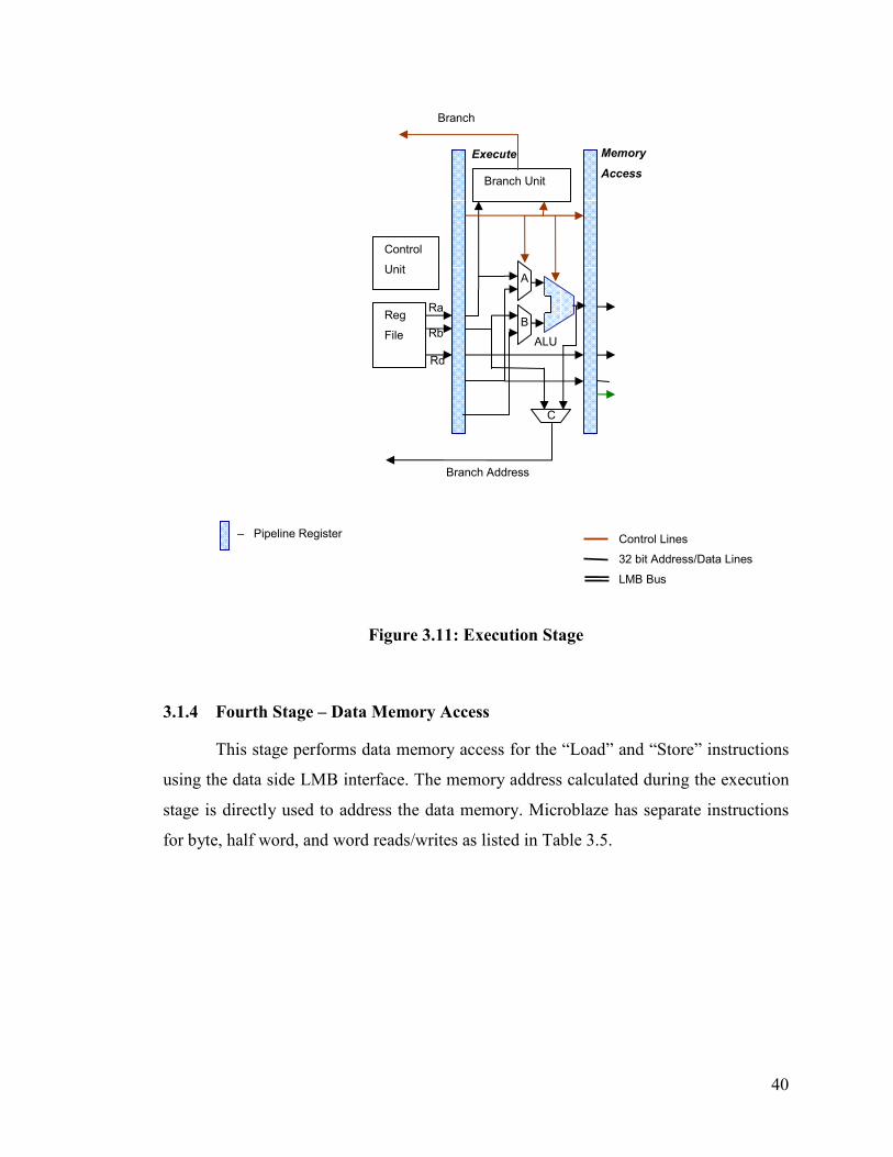
40
Figure 3.11: Execution Stage
3.1.4 Fourth Stage – Data Memory Access
This stage performs data memory access for the “Load” and “Store” instructions
using the data side LMB interface. The memory address calculated during the execution
stage is directly used to address the data memory. Microblaze has separate instructions
for byte, half word, and word reads/writes as listed in Table 3.5.
Control Lines
32 bit Address/Data Lines
LMB Bus
– Pipeline Register
Reg
File
Control
Unit
ALU
Branch Unit
Branch Address
Execute Memory
Access
Ra
Rb
Rd
Branch
A
B
C
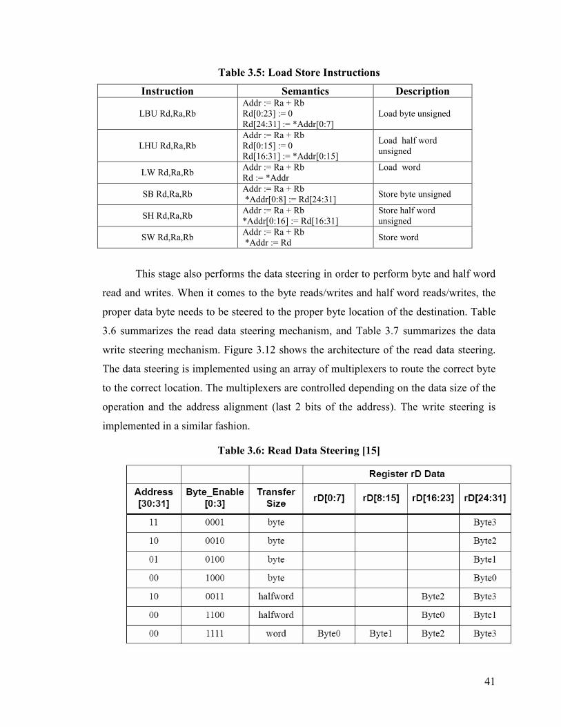
41
Table 3.5: Load Store Instructions
Instruction Semantics Description
LBU Rd,Ra,Rb Addr := Ra + Rb Rd[0:23] := 0 Rd[24:31] := *Addr[0:7]
Load byte unsigned
LHU Rd,Ra,Rb Addr := Ra + Rb Rd[0:15] := 0 Rd[16:31] := *Addr[0:15]
Load half word unsigned
LW Rd,Ra,Rb Addr := Ra + Rb Rd := *Addr
Load word
SB Rd,Ra,Rb Addr := Ra + Rb *Addr[0:8] := Rd[24:31] Store byte unsigned
SH Rd,Ra,Rb Addr := Ra + Rb *Addr[0:16] := Rd[16:31]
Store half word unsigned
SW Rd,Ra,Rb Addr := Ra + Rb *Addr := Rd
Store word
This stage also performs the data steering in order to perform byte and half word
read and writes. When it comes to the byte reads/writes and half word reads/writes, the
proper data byte needs to be steered to the proper byte location of the destination. Table
3.6 summarizes the read data steering mechanism, and Table 3.7 summarizes the data
write steering mechanism. Figure 3.12 shows the architecture of the read data steering.
The data steering is implemented using an array of multiplexers to route the correct byte
to the correct location. The multiplexers are controlled depending on the data size of the
operation and the address alignment (last 2 bits of the address). The write steering is
implemented in a similar fashion.
Table 3.6: Read Data Steering [15]
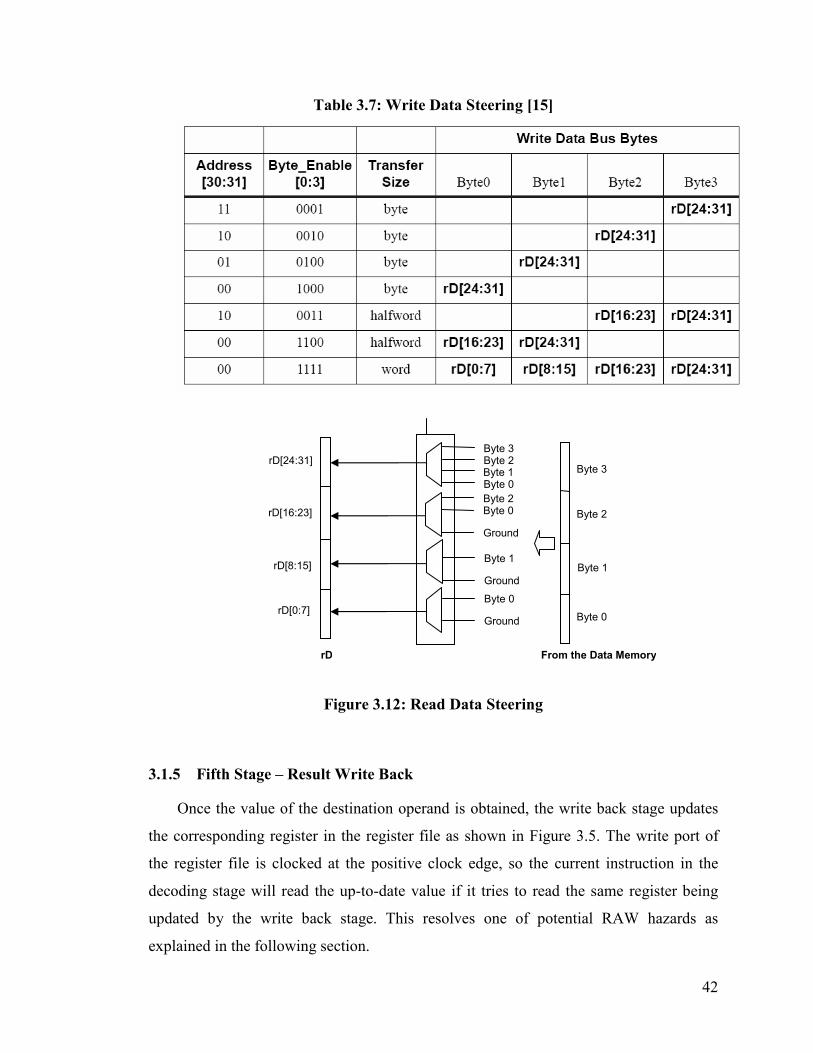
42
Table 3.7: Write Data Steering [15]
Figure 3.12: Read Data Steering
3.1.5 Fifth Stage – Result Write Back
Once the value of the destination operand is obtained, the write back stage updates
the corresponding register in the register file as shown in Figure 3.5. The write port of
the register file is clocked at the positive clock edge, so the current instruction in the
decoding stage will read the up-to-date value if it tries to read the same register being
updated by the write back stage. This resolves one of potential RAW hazards as
explained in the following section.
Byte 3 Byte 2 Byte 1 Byte 0
Byte 2 Byte 0
Ground
Byte 1
Ground
Byte 0
Ground rD[0:7]
rD[8:15]
rD[16:23]
rD[24:31]
rD From the Data Memory
Byte 0
Byte 1
Byte 2
Byte 3
43
3.1.6 Hazard Resolution
In order to overcome RAW data hazards (see section 2.6) due to the overlapped
execution of instructions, the base processor uses different mechanisms such as data
forwarding and pipeline stalling whenever possible.
RAW hazards occur whenever consecutive dependent (the destination register of an
instruction is used as one of source registers of a following instruction) instructions are
in progress as shown in
Table 3.8. For example, the “OR” instruction needs R2, calculated by “ADD”
instruction during the execution stage. However, the results of the “ADD” instruction
are still in Memory access stage. In order to overcome this hazard, data is forwarded
from the memory access stage to the execution stage.
Table 3.8: RAW Hazards in Progress
Fetch Decode Execute Mem. Acess Write Back
Instruction BEQ R5,R2 ADD R6,R2,R8 OR R5,R2,R3 ADD R2,R3,R4
The techniques used by the base processor to overcome these RAW hazards
whenever the dependent instructions are in the execution stage and in the memory access
stage are listed in Table 3.9 for generalized cases. The RAW hazards can also occur
when the dependant instructions are at the write back stage and at the execution stage.
This type of hazard is handled by forwarding the data from the write back stage to the
execution stage. During the situations where two dependant instructions are at the
decoding stage and at the write back stage, the RAW hazard still exists. This situation is
resolved by clocking the write port of the register file at the positive edge. Since the
pipeline is negative edge triggered, the dependent instruction at the decoding stage
always gets the up-to-date value from the register file, when progresses to the execution
stage. The data forwarding and stalling the appropriate stages are done by the hazard
control unit. The inputs of the ALU are multiplexed with the feedback operands from the
memory access and write back stages, so the hazard control unit can select the correct
operand to overcome the pipeline hazards.
44
Table 3.9: Hazard Resolution
The hazard control unit continuously monitors the destination and source operands in
each stage. Depending on the instruction type in each stage, the hazard control unit
generates appropriate control signals for stalling and forwarding. Figure 3.13 shows the
hazard control unit and the forwarding paths connected through the multiplexers to the
inputs of the ALU. Overlapped execution of instructions due to pipelining also
introduces control hazards. When a branch is resolved at the execution stage, and if it is
taken, the instruction in the decoding stage continues to execute. This type of hazard is
known as a control hazard, and two simple methods can be used to resolve this hazard.
The first method is to flush the decoding stage, and the second method is to allow the
instruction to complete. The latter method is known as “delay slots”, where the
instruction following the branch is always executed in the pipeline irrespective of the
outcome of the branch. MicroBlaze architecture addresses this issue using both methods.
Microblaze branch instructions have two variations where one format uses a delay slot
and the other uses pipeline flushes. The base processor uses the same mechanism to
overcome control hazards due to branch instructions in order to maintain the cycle
accuracy with Microblaze. For the branch instruction without a delay slot, the decoding
stage is flushed once the branch is resolved during the execution stage. For the branch
instructions with a delay slot, the instruction in the decoding stage is allowed to
complete.
Instruction type
at mem. access
stage
Instruction
type at exe.
stage
Hazard resolution techniques used
ALU operation ALU or branch
operation Data forwarded from the memory access stage to the execution stage.
Memory
operation
Memory
operation
Execution stage stalled.
Data forwarded from the memory access stage to the execution stage.
Memory
operation ALU operation
Execution stage stalled.
Data forwarded from the memory access stage to the execution stage.
Memory
operation
Branch
operation
Execution stage stalled.
Data forwarded from the memory access stage to the execution stage.

45
Figure 3.13: Base Processor Pipeline with Hazard Control
46
3.2 Architecture of RTOS
The second phase of this thesis extends the base processor with hardware RTOS
support. This section examines the internal architecture of the software RTOSs, and the
next section presents the concept and design of RTBlaze, a multithreaded processor with
integrated RTOS functions in hardware.
RTOSs provide various services for the applications that run on top of the OS. The
most important service provided by the RTOS is multithreading. The application
programs can use multiple threads to perform various tasks concurrently. OSs use time
multiplexing of each thread to achieve the concurrent behavior. Conventional RTOSs
implement multithreading support in software on top of the basic instruction set
architecture and interrupt handling mechanism of the processor.
Multithreading introduces different issues such as synchronization among threads.
OSs provides a rich set of services to alleviate those issues due to multithreading. The
application software can access these services through a special mechanism called
system calls. Table 3.10 summarizes some basic system calls available in the Xilkernal
[56].
Table 3.10: Basic System Calls Provided by a RTOS
System call Description
pthread_create Creates a new thread
pthread_exit Kills the thread pointed by TID in Ra.
register_int_handler Creates an interrupt thread
acknowledge_interrupt Clears the interrupt.
disable_interrupt Kills the interrupt thread.
sleep Put the thread into sleep state for specific amount of time
sem_init Initialize a semaphore
sem_wait Wait operation on a semaphore
sem_post Post operation on a semaphore
The concept of multithreading is layered on top of a thread switching mechanism
called context switching. Switching between the threads is used to emulate the
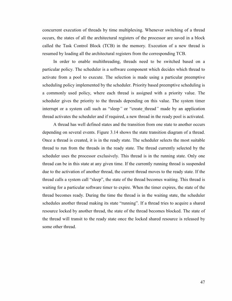
47
concurrent execution of threads by time multiplexing. Whenever switching of a thread
occurs, the states of all the architectural registers of the processor are saved in a block
called the Task Control Block (TCB) in the memory. Execution of a new thread is
resumed by loading all the architectural registers from the corresponding TCB.
In order to enable multithreading, threads need to be switched based on a
particular policy. The scheduler is a software component which decides which thread to
activate from a pool to execute. The selection is made using a particular preemptive
scheduling policy implemented by the scheduler. Priority based preemptive scheduling is
a commonly used policy, where each thread is assigned with a priority value. The
scheduler gives the priority to the threads depending on this value. The system timer
interrupt or a system call such as “sleep” or “create_thread” made by an application
thread activates the scheduler and if required, a new thread in the ready pool is activated.
A thread has well defined states and the transition from one state to another occurs
depending on several events. Figure 3.14 shows the state transition diagram of a thread.
Once a thread is created, it is in the ready state. The scheduler selects the most suitable
thread to run from the threads in the ready state. The thread currently selected by the
scheduler uses the processor exclusively. This thread is in the running state. Only one
thread can be in this state at any given time. If the currently running thread is suspended
due to the activation of another thread, the current thread moves to the ready state. If the
thread calls a system call “sleep”, the state of the thread becomes waiting. This thread is
waiting for a particular software timer to expire. When the timer expires, the state of the
thread becomes ready. During the time the thread is in the waiting state, the scheduler
schedules another thread making its state “running”. If a thread tries to acquire a shared
resource locked by another thread, the state of the thread becomes blocked. The state of
the thread will transit to the ready state once the locked shared resource is released by
some other thread.
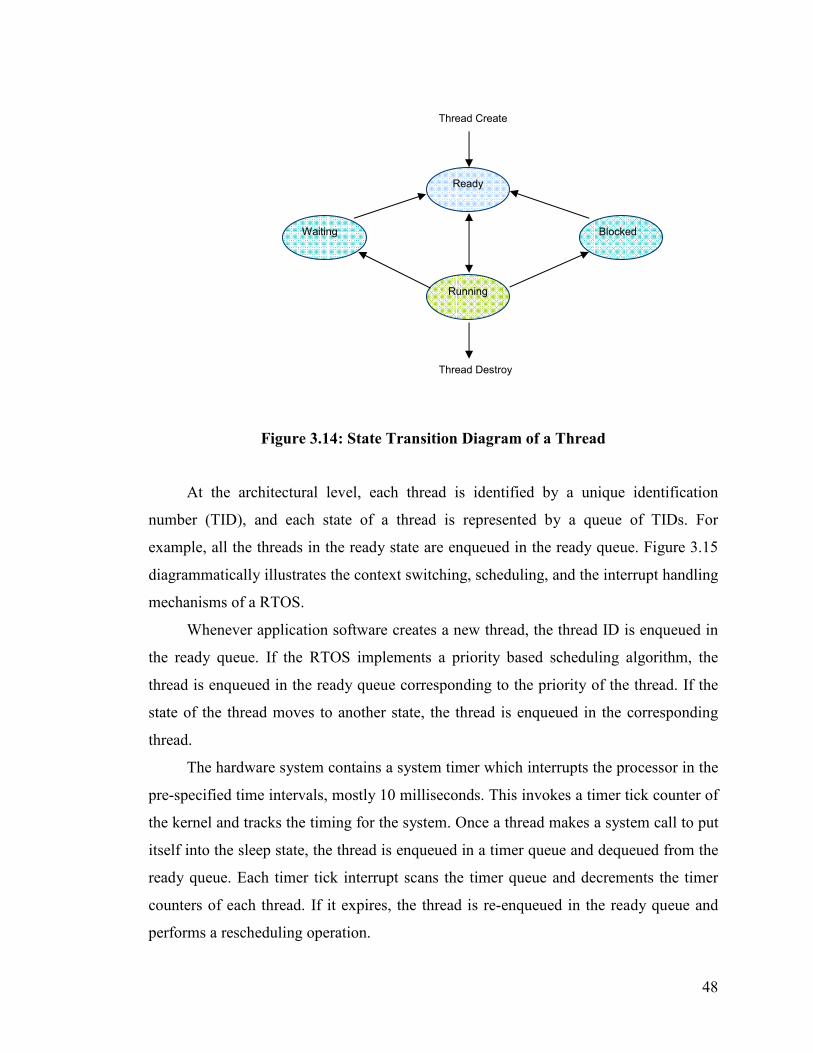
48
Figure 3.14: State Transition Diagram of a Thread
At the architectural level, each thread is identified by a unique identification
number (TID), and each state of a thread is represented by a queue of TIDs. For
example, all the threads in the ready state are enqueued in the ready queue. Figure 3.15
diagrammatically illustrates the context switching, scheduling, and the interrupt handling
mechanisms of a RTOS.
Whenever application software creates a new thread, the thread ID is enqueued in
the ready queue. If the RTOS implements a priority based scheduling algorithm, the
thread is enqueued in the ready queue corresponding to the priority of the thread. If the
state of the thread moves to another state, the thread is enqueued in the corresponding
thread.
The hardware system contains a system timer which interrupts the processor in the
pre-specified time intervals, mostly 10 milliseconds. This invokes a timer tick counter of
the kernel and tracks the timing for the system. Once a thread makes a system call to put
itself into the sleep state, the thread is enqueued in a timer queue and dequeued from the
ready queue. Each timer tick interrupt scans the timer queue and decrements the timer
counters of each thread. If it expires, the thread is re-enqueued in the ready queue and
performs a rescheduling operation.
Ready
Running
Waiting Blocked
Thread Create
Thread Destroy
49
Figure 3.15: Simplified Architecture of a RTOS Kernel Running On a SOPC
In order to synchronize multiple threads, semaphores are provided by most OSs. A
semaphore consists of a counter and a queue. Whenever a thread creates a new
semaphore, the semaphore counter gets loaded with the requested semaphore value. A
thread can wait for a given semaphore by performing a wait operation on the semaphore
Context
Switching
Kernel and
Scheduler
TCBs
Ready
Queues
Timer
Queue
Semaphore
Queues
CPU
RTOS
Application
Software
Threads
Interrupt
Controller
Timer
Interrupt
Priority 0
Priority n
Global
Interrupt
Handler
Software
Hardware
Memory
Timer
Thread ID
External
Interrupts
50
which results in decrementing its semaphore value. If the decremented value is less than
zero, the thread which performed the wait operation is dequeued from the ready queue.
Next, the thread is enqueued in the semaphore queue causing the thread to move to the
blocked state from the running state. Any further wait operations on the semaphore
cause the corresponding thread to be enqueued in the semaphore queue. When a thread
performs a post operation on the semaphore, its value is incremented. If the result is
equal to zero or greater, the highest priority thread in the semaphore wait queue is
dequeued and enqueued in the ready queue.
Software RTOSs use layered interrupt handling mechanism. General purpose
processors have single hardware interrupt and external interrupt controller [57] which
are used to support multiple interrupt request lines (IRQs). OSs install a global handler
for the main interrupt to resolve the correct ID of the external interrupt by accessing the
external interrupt controller. Once resolved, the global handler calls the corresponding
interrupt service routing in the application space. Some RTOSs use a mechanism to
delegate the task of interrupt handling to application level threads called interrupt service
threads (ISTs). In this case, the global interrupt handler enqueues the IST waiting for the
corresponding IRQ in the ready queue, enabling the system to respond to further IRQs
about to occur.
In the context of real-time systems, the software implementations of
multithreading incur considerable overhead and contribute to increased nondeterministic
behavior of the system as well as slower response. The layered approach to resolve the
interrupt IDs introduces substantial interrupt latency. Most software mechanisms have
the feature of the paralizability and are good candidates for direct hardware level
implementation. For example, the priority based scheduler can be implemented by a
priority decoder. The next section describes the design of RTBlaze, which implements
RTOS mechanisms in hardware.
51
3.3 Design of the RTBlaze
The main goal of the second phase of the thesis is to migrate software mechanisms
of software RTOS mentioned in the previous section into hardware in order to eliminate
the overhead associated with software implementations. To accomplish this, the
instruction set of the base processor is augmented with support for the following OS
level operations.
• Multithreading (thread creation/deletion)
• Interrupt service threads
• Timers
• Semaphores
Table 3.11 summarizes the RTBlaze instructions related to the RTOS functions. The
current RTBlaze prototype implements a lightweight version of basic system calls of a
RTOS. The “FORK” and “KILL” instructions are used for thread creation and deletion.
The interrupt mechanism is handled using the “IFORK”, “IKILL” and “ICLEAR”
instructions while semaphore functions are accessed using the “SEMWAIT”,
“SEMINIT” and “SEMPOST” instructions.
Instruction set extension for RTOS services is integrated to the base processor
pipeline by modifying and extending the pipeline with support for following entities.
• Context switching
• Thread scheduling
• Timers
• Semaphores
• Interrupts
52
Table 3.11: RTBlaze Instructions for RTOS Services
Instruction Description
FORK Rd, Ra, Rb
A new thread is created and placed in the ready queue. The value
of Ra is used as the thread ID. Thread ID itself represent the
priority of the thread being created. Rb points to the address of
the first instruction to be executed when the thread is in run mode.
KILL Rd, Ra, Kills the thread pointed by TID in Ra.
SLEEP Rd,Ra Current thread is enqueued in the timer queue and is awakened
after the cycles specified by Ra.
IFORK Rd, Ra, Rb
A new thread is created and corresponding interrupt line is
enabled. The value of Ra is used as the interrupt ID. Interrupt ID
itself represent the priority of the thread being created. Rb points
to the address of the first instruction to be executed when the
interrupt is occurred.
ICLEAR Rd,Ra, Rb
Clears the interrupt. The value of Ra is used as the interrupt ID.
interrupt ID itself represents the priority of the thread being
created. Rb points to the address of the first instruction to be
executed when the interrupt occurs.
IKILL Rd,Ra Kills the interrupt thread pointed by TID in Ra.
SEMINIT Rd,Ra,Rb Initialize the count value of the semaphore identified by Ra. The
initial value of the semaphore is set to Rb.
SEMWAIT Rd,Ra
Increments the count value of the semaphore specified in Ra. If
the result is positive or zero the highest priority thread dequeued
from the semaphore wait queue and placed in the ready queue.
SEMPOST Rd,Ra
Decrement the count value of the semaphore by 1. If the result is
smaller than zero, the current thread is dequeued from the ready
queue and placed in the corresponding semaphore wait queue.
Semaphore ID is specified in Ra.
Figure 3.16 shows the base processor with architectural extensions for RTOS
support. In comparison with the software RTOSs, the operation is conceptually the same,
but realized in hardware and operates in a parallel fashion. Hardware based mechanism
for context switching is realized using the concept of multithreading. The base pipeline
is extended with support for multithreading by replicating all the architectural registers
for each thread and propagating a unique thread ID to identify the correct register space
(or the context) with each instruction. The scheduler module implements a static priority
53
based preemptive scheduler in hardware. Depending on the priority, the scheduler
decides the next ready thread to run and propagates the selected thread ID to the
multithreaded pipeline in order to switch to the context of the newly selected thread.
Timers are implemented as independent hardware counters, thus, processor intervention
for scanning the timer queues and counting down is not required. The semaphore module
also performs all the operations in hardware in a parallel fashion. RTBlaze implements
fast interrupt handling mechanism by directly mapping the ISTs to the hardware threads.
This introduces another possible state for the RTBlaze threads as shown in Figure 3.17.
Once created with the “IFORK” instruction the IST is in the waiting-for-IRQ state. Upon
the occurrence of an external interrupt, the corresponding IST is enqueued in the ready
queue, and the scheduler will select the IST depending on the priority.
Figure 3.16: Base Processor with RTOS Extension
Base Processor
Scheduler
Timers
Semaphores
Context
Switching
External
Interrupts
Ready
Queue
Multithreaded Processor
54
Figure 3.17: State Transition Diagram of an RTBlaze Thread
The modified pipeline of the base processor is shown in Figure 3.18. Multithreading
support is added to the base processor pipeline by propagating the thread ID down the
pipeline and replicating the register file for each thread. The selected thread ID is
propagated through each pipeline stage with the instruction. This always guarantees that
during the register file access, the correct register set is addressed. This is accomplished
by appending the thread ID to each register address field of the instruction. The register
write address is also qualified with the thread ID propagated to the writeback stage alone
with the instruction. The writeback stage always writes to the correct register set even if
the register file is being accessed by an instruction from another thread. Since the
pipeline supports block interleaved multithreading, the hazard detection logic is always
qualified with the thread IDs.
In order to enable multithreading, a thread scheduler with a program counter bank is
introduced to the fetch stage. The scheduler decides the next thread to be executed, and
the program counter bank stores all the distinct program counters associated with each
thread. The scheduler supports a maximum of 16 threads with unique priority values
ranging from 0 to 15. The thread ID is also used as the priority of the thread. This
concept simplifies the hardware, but the application programs have to track the
currently-used thread IDs. TID zero is the lowest priority, and the thread associated with
Ready
Running
Waiting Blocked
Thread Create
Waiting
for IRQ
IST Create
Thread Destroy
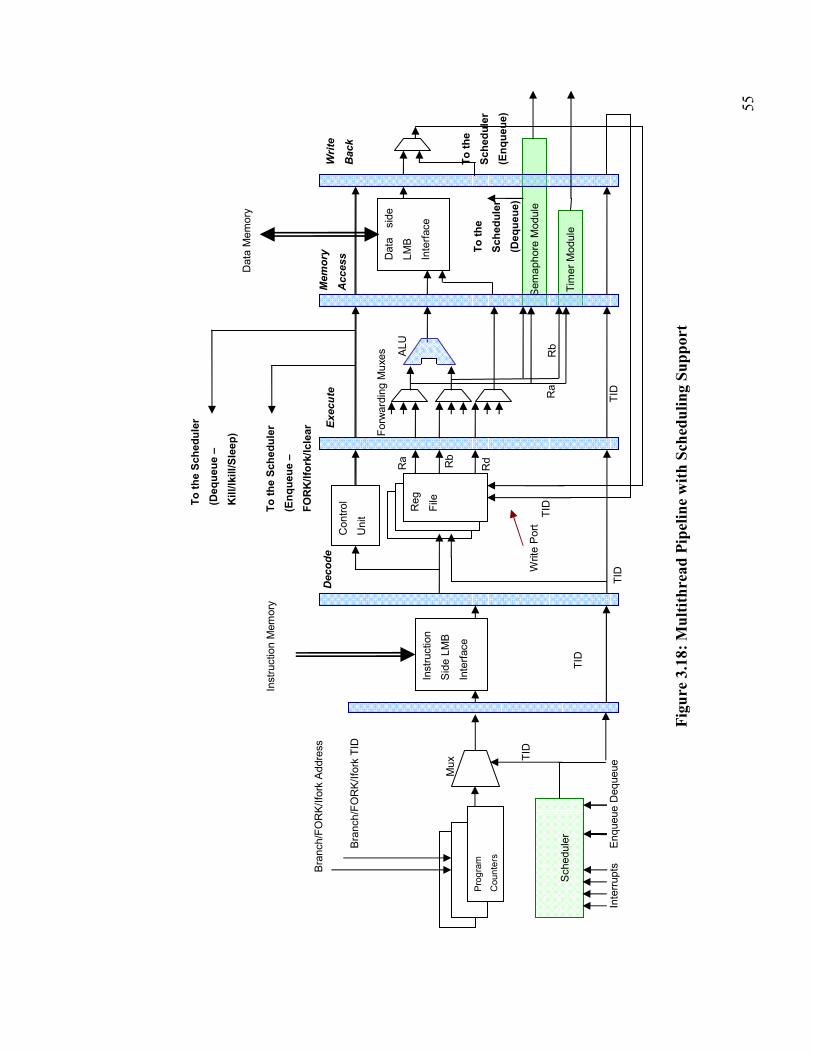
55
Figure 3.18: Multithread Pipeline with Scheduling Support
To the
Scheduler
(Enqueue)
To the
Scheduler
(Dequeue)
Tim
er
Module
Sem
aphore
Module
R
eg
File
TID
TID
Decode
Write
Port
Execute
Data
sid
e
LM
B
Inte
rface
Data
Mem
ory
Memory
Access
TID
Write
Back
Contr
ol
Unit To the Scheduler
(Enqueue –
FORK/Ifork/Iclear
To the Scheduler
(Dequeue –
Kill/Ikill/Sleep)
Ra
Rb
ALU
R
a
Rb
Rd
Forw
ard
ing M
uxes
Schedule
r
Instr
uction
Sid
e L
MB
Inte
rface
Pro
gra
m
Coun
ters
TID
TID
Bra
nch/F
OR
K/I
fork
Addre
ss
Mu
x
Bra
nch/F
OR
K/I
fork
TID
Inte
rrupts
E
nqueue D
equeue
Instr
uction M
em
ory

56
TID zero is automatically created upon reset and starts executing from address
0x00000000.
The timer module is aligned with the memory access stage of the pipeline. The
semaphore module itself is pipelined and aligned with both the memory access and write
back stage of the pipeline. Both timer and semaphore related instructions use register
operands (Ra and Rb) as their source values. These alignments help reuse existing
forwarding paths to eliminate RAW hazards. The control unit is also modified to support
decoding of those new instructions, and it generates the appropriate signals to manage
the semaphore and timer modules. For example, whenever the decoding stage decodes a
sleep instruction, it generates the control signals to dequeue the current thread from the
ready queue. Appropriate control signals to load the timers with the corresponding value
are also generated by the control unit.
Execution of this OS level instruction may cause preemption of the current thread
and rescheduling of another thread. For example, if a “FORK” instruction is in progress
in the pipeline, the execution stage resolves the operands of the “FORK” and enqueues
the TID in the ready queue. If the newly created thread has the highest priority among
other ready threads, the current thread gets preempted by this new thread. In this case,
the instructions in the previous pipeline stages need to be flushed or defined as delay
slots. RTBlaze uses later approach, since the simplicity inherent to the use of delay slots
make the processor design straightforward.
The following sections present an elaborated discussion on the architectural
extensions made to the base multithreaded processor in order to augment the instruction
set with RTOS support.
3.3.1 The Fetch Stage with Scheduling Support
The scheduler contains a priority encoder attached to the ready queue. The ready
queue is implemented in a parallel fashion. Therefore multiple elements can be updated
simultaneously. The program counter bank is implemented using a dual port block RAM
memory block.
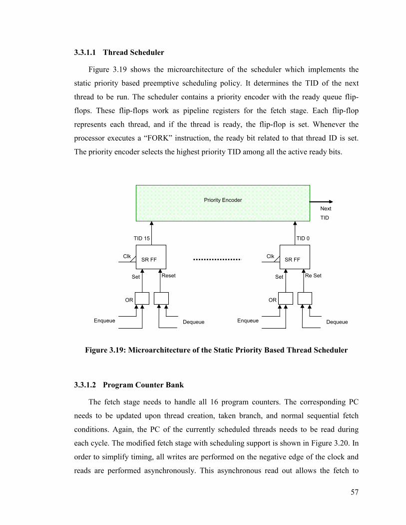
57
3.3.1.1 Thread Scheduler
Figure 3.19 shows the microarchitecture of the scheduler which implements the
static priority based preemptive scheduling policy. It determines the TID of the next
thread to be run. The scheduler contains a priority encoder with the ready queue flip-
flops. These flip-flops work as pipeline registers for the fetch stage. Each flip-flop
represents each thread, and if the thread is ready, the flip-flop is set. Whenever the
processor executes a “FORK” instruction, the ready bit related to that thread ID is set.
The priority encoder selects the highest priority TID among all the active ready bits.
Figure 3.19: Microarchitecture of the Static Priority Based Thread Scheduler
3.3.1.2 Program Counter Bank
The fetch stage needs to handle all 16 program counters. The corresponding PC
needs to be updated upon thread creation, taken branch, and normal sequential fetch
conditions. Again, the PC of the currently scheduled threads needs to be read during
each cycle. The modified fetch stage with scheduling support is shown in Figure 3.20. In
order to simplify timing, all writes are performed on the negative edge of the clock and
reads are performed asynchronously. This asynchronous read out allows the fetch to
TID 15 TID 0
Enqueue
OR
Re Set
Clk
Reset Set
Priority Encoder
SR FF Clk
Set
SR FF
Next
TID
Dequeue Enqueue
OR
Dequeue
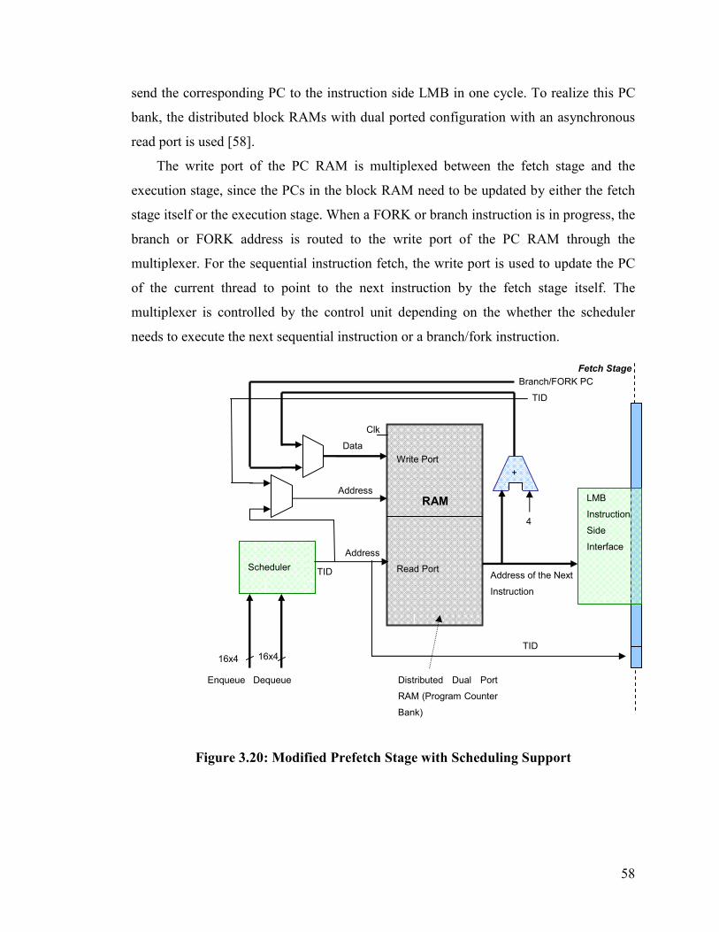
58
send the corresponding PC to the instruction side LMB in one cycle. To realize this PC
bank, the distributed block RAMs with dual ported configuration with an asynchronous
read port is used [58].
The write port of the PC RAM is multiplexed between the fetch stage and the
execution stage, since the PCs in the block RAM need to be updated by either the fetch
stage itself or the execution stage. When a FORK or branch instruction is in progress, the
branch or FORK address is routed to the write port of the PC RAM through the
multiplexer. For the sequential instruction fetch, the write port is used to update the PC
of the current thread to point to the next instruction by the fetch stage itself. The
multiplexer is controlled by the control unit depending on the whether the scheduler
needs to execute the next sequential instruction or a branch/fork instruction.
Figure 3.20: Modified Prefetch Stage with Scheduling Support
Write Port
RAM
Read Port
Scheduler
Distributed Dual Port
RAM (Program Counter
Bank)
+
4
LMB
Instruction
Side
Interface
Branch/FORK PC
TID
Address of the Next
Instruction
Clk
Data
Address
TID
Address TID
16x4 16x4
Enqueue Dequeue
Fetch Stage
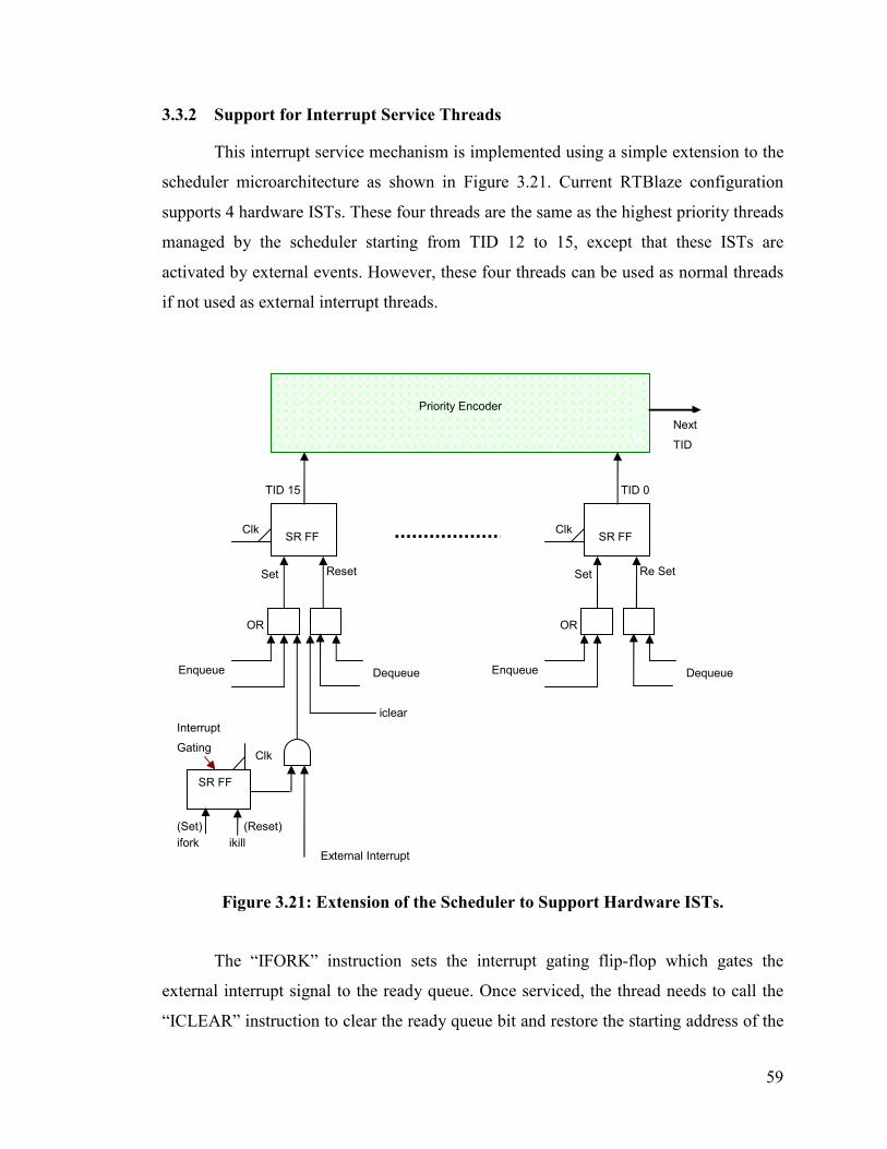
59
3.3.2 Support for Interrupt Service Threads
This interrupt service mechanism is implemented using a simple extension to the
scheduler microarchitecture as shown in Figure 3.21. Current RTBlaze configuration
supports 4 hardware ISTs. These four threads are the same as the highest priority threads
managed by the scheduler starting from TID 12 to 15, except that these ISTs are
activated by external events. However, these four threads can be used as normal threads
if not used as external interrupt threads.
Figure 3.21: Extension of the Scheduler to Support Hardware ISTs.
The “IFORK” instruction sets the interrupt gating flip-flop which gates the
external interrupt signal to the ready queue. Once serviced, the thread needs to call the
“ICLEAR” instruction to clear the ready queue bit and restore the starting address of the
Reset
ifork
TID 15 TID 0
Enqueue
OR
Re Set
Clk
Set
Priority Encoder
SR FF Clk
Set
SR FF
Next
TID
Dequeue
iclear
Enqueue
OR
Dequeue
SR FF
Clk
External Interrupt ikill
(Reset) (Set)
Interrupt
Gating

60
IST. The “IKILL” instruction disables the interrupt by clearing the interrupt gating flip
flop. This is equivalent to the interrupt disable functions of software RTOSs. Upon the
reception of an interrupt, the corresponding hardware IST is scheduled during the next
cycle if it is the highest priority thread currently in the ready state.
3.3.3 Hardware Timers
The RTBlaze support 15 hardware timers. The thread ID zero is not associated with
a timer, since it is the idle thread and is supposed to be run whenever no other thread is
ready. A thread can be put into the sleep state by executing the “SLEEP” instruction.
The timers are implemented in direct mapped fashion with parallel execution. Figure
3.22 shows the microarchitecture of the direct mapped hardware timers. The timers do
not consume any CPU cycles and the expiration is cycle accurate. This allows realizing
high precision timers with the precision in a nanosecond scale provided that the thread
requesting the timing is the highest priority thread currently active. Upon the execution
of a “SLEEP” instruction by a thread, its timer is loaded with the number of cycles
requested, and the thread is deactivated in the scheduler. The thread ID at the execution
stage is used to enable the loading of the corresponding hardware timer through a
decoder. Each element of the timer queue has its own down counter, and upon the
expiration of the timer queue element the corresponding thread ID is reactivated in the
ready queue.

61
Figure 3.22: Direct Mapped Hardware Timers
3.3.4 Hardware Semaphores
When it comes to the multithreaded processors, they have the possibility to
implement full hardware support for blocked synchronization schemes. Bradford, J.P.
and S. Abraham [59] propose a blocking synchronization mechanism for multithreaded
processors. The semaphore counters are stored in the memory and special semaphore
handling instructions update those values according to the semaphore operations being
performed. This scheme enables globally accessible semaphores in a context of a
multiprocessor system. RTBlaze uses full hardware implementation of semaphores in
order to provide an efficient mechanism for thread synchronization. The RTBlaze
scheme is local to the processor and cannot be used to synchronize the thread in a
different processor. However, unlike the scheme of Bradford, J.P. and S. Abraham, the
RTBlaze implementation of semaphores results in zero overhead semaphore operations
since this scheme does not use external memory for semaphore counters.
Load
Din
Load
Enable
Enqueue (TID 1)
Enqueue (TID 15)
Timer Counter
Timer Counter
To the
Scheduler
Ra Sleep TID
Expiration Detection
Expiration Detection
Execute Stage Memory Stage
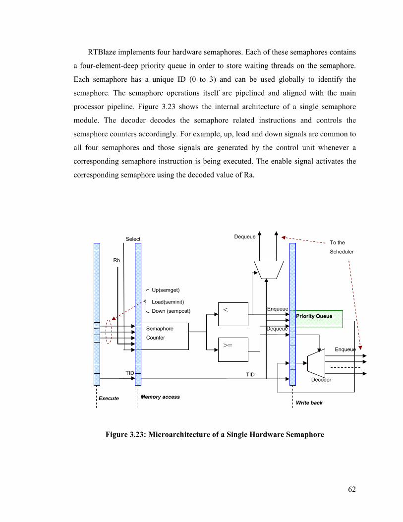
62
RTBlaze implements four hardware semaphores. Each of these semaphores contains
a four-element-deep priority queue in order to store waiting threads on the semaphore.
Each semaphore has a unique ID (0 to 3) and can be used globally to identify the
semaphore. The semaphore operations itself are pipelined and aligned with the main
processor pipeline. Figure 3.23 shows the internal architecture of a single semaphore
module. The decoder decodes the semaphore related instructions and controls the
semaphore counters accordingly. For example, up, load and down signals are common to
all four semaphores and those signals are generated by the control unit whenever a
corresponding semaphore instruction is being executed. The enable signal activates the
corresponding semaphore using the decoded value of Ra.
Figure 3.23: Microarchitecture of a Single Hardware Semaphore
<
>=
Priority Queue
Semaphore
Counter
Dequeue
Enqueue
Memory access Write back
Execute
To the
Scheduler
Enqueue
TID
Dequeue
Up(semget)
Load(seminit)
Down (sempost)
Rb
Select
Decoder
TID

63
The semaphore operations are conceptually equivalent with the software based
realizations. For example, the “SEMINIT” instruction loads the semaphore counter
register identified by the value in Ra with the value in Rb. The “SEMWAIT” instruction
decrements the semaphore counter value by one during the memory access stage. The
comparison of the result is accomplished using dedicated comparators, and if the counter
value is less than zero, the current TID is dequeued from the ready queue and enqueued
in the priority queue. Both the enqueue and dequeue operations occur in write back
stage. The “SEMPOST” operation increments the semaphore counter value, and if the
value is zero or greater than zero, the top TID is enqueued from the priority queue and
the corresponding thread is reactivated in the scheduler. Once enqueued in the
semaphore wait queue, the items need to be removed according to the priority of the
waiting threads. The highest priority thread needs to be removed first in order to prevent
deadlocks. The priority queue [60] is implemented in hardware using the parallel version
of the insertion sort algorithm. When the thread ID is inserted in the queue, it is placed in
the corresponding location according to its value, and the queue items are automatically
rearranged.
The priority queue is implemented using cascaded active queue elements. The
microarchitecture of a single queue element is shown in Figure 3.24. Whenever a new
thread ID needs to be inserted, the ID is transmitted to all the queue elements. Only one
queue element latches the new entry depending on the comparison results. All other
elements keep their values unchanged or shift down their values along the queue
depending on the comparison results. This results in the implementation of the parallel
version of the insertion sort algorithm. Therefore, an item can be inserted in the queue in
a single cycle. The head of the queue always has the highest priority item which can be
dequeued in a single cycle.
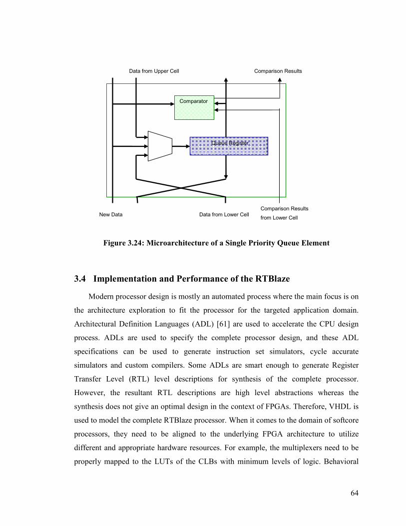
64
Figure 3.24: Microarchitecture of a Single Priority Queue Element
3.4 Implementation and Performance of the RTBlaze
Modern processor design is mostly an automated process where the main focus is on
the architecture exploration to fit the processor for the targeted application domain.
Architectural Definition Languages (ADL) [61] are used to accelerate the CPU design
process. ADLs are used to specify the complete processor design, and these ADL
specifications can be used to generate instruction set simulators, cycle accurate
simulators and custom compilers. Some ADLs are smart enough to generate Register
Transfer Level (RTL) level descriptions for synthesis of the complete processor.
However, the resultant RTL descriptions are high level abstractions whereas the
synthesis does not give an optimal design in the context of FPGAs. Therefore, VHDL is
used to model the complete RTBlaze processor. When it comes to the domain of softcore
processors, they need to be aligned to the underlying FPGA architecture to utilize
different and appropriate hardware resources. For example, the multiplexers need to be
properly mapped to the LUTs of the CLBs with minimum levels of logic. Behavioral
Queue Register
Comparator
New Data Data from Lower Cell
Data from Upper Cell Comparison Results
Comparison Results
from Lower Cell
65
level of design does not always give the optimum synthesis results even if advanced
optimization features of the synthesis engine are enabled. Xilinx XST optimizations and
structural level modeling is used throughout the design in order to maximally align the
processor core with the Vertex II pro FPGA architecture. This helps to reduce the
resource usage as well as the wastage while maximizing the maximum clock frequency.
When targeted Vertex II pro, RTBlaze can be clocked up to a maximum of 119MHz.
66
Chapter 4
Results
The first section of this chapter presents the validation results of the base processor
and the RTBlaze. The second part of this chapter compares the RTBlaze performance
with some RTOS kernels. This chapter further investigates the chip area increase due to
hardware RTOS attachment to the base processor.
4.1 Simulation Results
Simulation of the system is done using the Mentor Graphics ModelSim SE
simulator. Simple assembly programs are used to simulate the basic functionality of the
processor. The base processor is validated using random instructions from different
categories, and the RTOS features of RTBlaze are validated using simple assembly
programs.

67
4.1.1 Base Processor Validation
Even though the current prototype of the base processor implements more than 70
instructions, not all of the instructions are validated. A subset of those instructions
belongs to different categories is validated using some random instruction sequence.
Table 4.1 shows the simple assembly program used to validate some of arithmetic and
branch instructions.
Table 4.1: Assembly Program Used to Validate Arithmetic and Branch Instructions
# Memory Address Contents Instruction Description
1 0x00000020 0x21800008 ADDI R12,R0,0x8 Load R12 with 0x8
2 0x00000024 0x 21A00002 ADDI R13,R0,0x2 Load R13 with 0x2
3 0x00000028 0x058D6000 RSUB R12,R13,R12 R12 = R12-R13
4 0x0000002C 0xBC8CFFFC BGTI R12,-0x4 Branch PC - 0x4 if R12 is greater
than 0
5 0x00000030 0x21C00001 ADDI R14,R0,0x1 Load R14 with 0x1
6 0x00000034 0x01EE6800 ADD R15,R14,R13 R15 = R14+ r 13
First, two instructions load the corresponding registers with the immediate values
provided with the instruction. The third instruction uses both R12 and R13 to execute,
but the results are still not available in the register file. Therefore the hazard detection
and control unit forward the results of the first and second instructions. The branch target
is calculated using the immediate value provided with the instruction. The ALU is used
to calculate this address with the special mode where the first operand (the program
counter) is regarded as an unsigned value.
Whenever the branch occurs, the 5th and 6th instructions enter to the pipeline since
the branch is resolved in the execution stage. Both these instructions are flushed at the
decoding stage, so two bubbles (no-operations) are propagated in the pipeline. Figure
4.1, Figure 4.2, Figure 4.3, Figure 4.4, Table 4.3, and Table 4.2 illustrate the simulation
results.
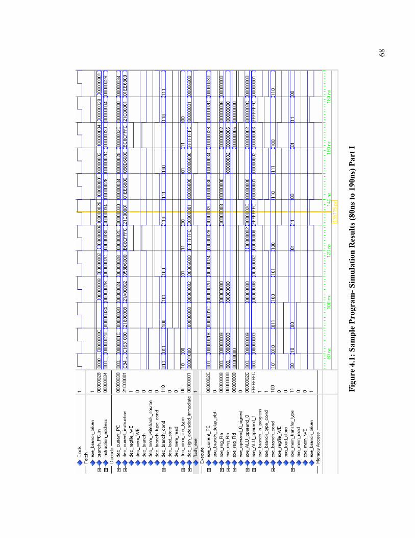
68
Figure 4.1: Sample Program- Simulation Results (80ns to 190ns) Part I
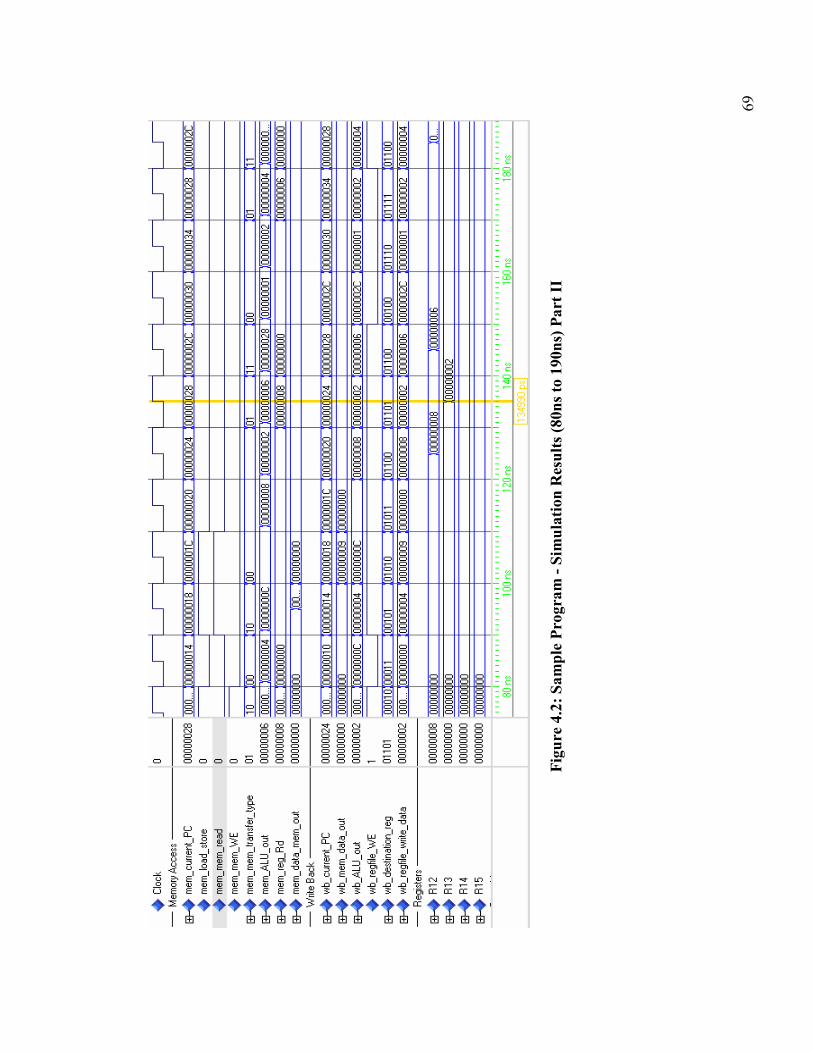
69
Figure 4.2: Sample Program - Simulation Results (80ns to 190ns) Part II
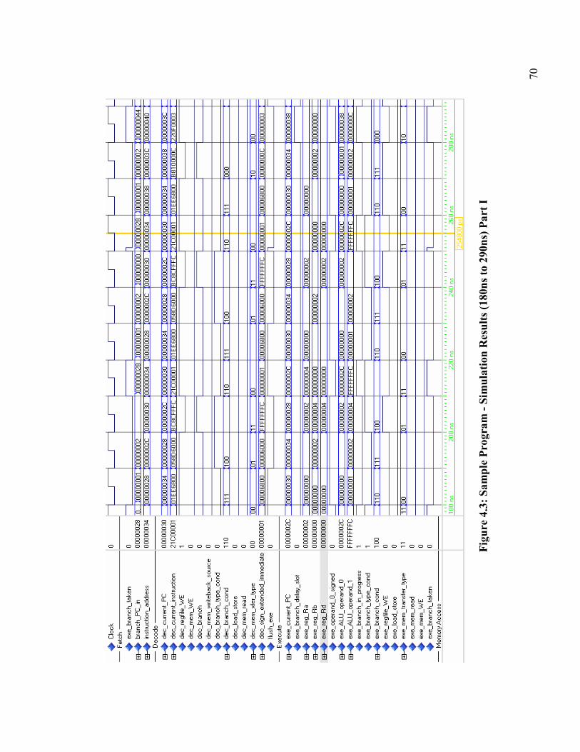
70
Figure 4.3: Sample Program - Simulation Results (180ns to 290ns) Part I
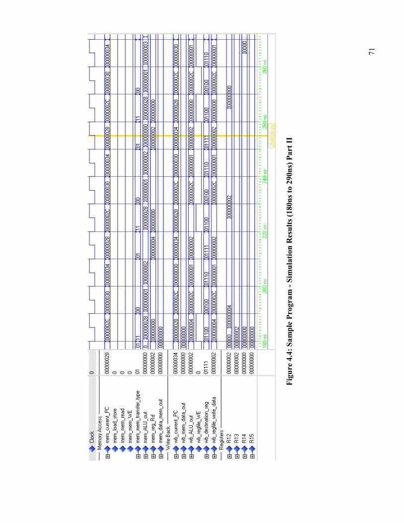
71
Figure 4.4: Sample Program - Simulation Results (180ns to 290ns) Part II
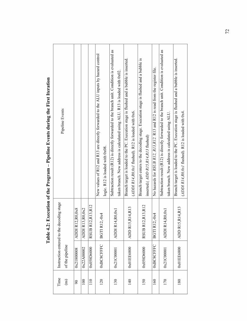
72
Table 4.2: Execution of the Program – Pipeline Events during the First Iteration
Tim
e
(ns)
Instruction entered to th
e decoding stage
of th
e pipeline
Pipeline Events
90
0x21
800008
ADDI R12
,R0,0x8
100
0x22
A00
002
ADDI R13
,R0,0x2
110
0x05
8D60
00
RSUB R12
,R13
,R12
120
0xBC8C
FFFC
BGTI R12
,-0x4
New
values of R12
and R13
are directly forw
arded to th
e ALU in
puts by hazard control
logic. R12
is lo
aded with 0x08
.
130
0x21
C00
001
ADDI R14
,R0,0x1
Subtraction result (R12
) is directly forw
arded to th
e branch unit. Condition
is evaluated as
taken branch. N
ew add
ress is calculated using ALU. R
13 is lo
aded with 0x02
.
140
0x01
EE68
00
ADD R15
,R14
,R13
Branch target is lo
aded to
the PC. E
xecution stage is flushed and a bubble is in
serted.
(ADDI R14,R0,0x1 flushed). R12
is lo
aded with 0x
6.
150
0x05
8D60
00
RSUB R12
,R13
,R12
Branch target enters to th
e decoding stage. E
xecution stage is flushed and a bubble is
inserted.( ADD R15,R14,R13 flushed)
160
0xBC8C
FFFC
BGTI R12
,-0x4
No hazards for RSUB R12, R13,R12. R13
and R12
is read from
the register file.
170
0x21
C00
001
ADDI R14
,R0,0x1
Subtraction result (R12
) is directly forw
arded to th
e branch unit. Condition
is evaluated as
taken branch. N
ew add
ress is calculated using ALU.
180
0x01
EE68
00
ADD R15
,R14
,R13
Branch target is lo
aded to
the PC. E
xecution stage is flushed and a bubble is in
serted.
(ADDI R14,R0,0x1 flushed). R12
is lo
aded with 0x
4.
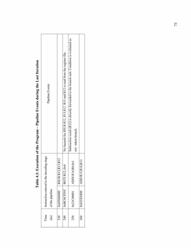
73
Table 4.3: Execution of the Program – Pipeline Events during the Last Iteration
Tim
e
(ns)
Instruction entered to th
e decoding stage
of th
e pipeline
Pipeline Events
230
0x05
8D60
00
RSUB R12
,R13
,R12
240
0xBC8C
FFFC
BGTI R12
,-0x4
No hazards for RSUB R12, R13,R12. R13
and R12
is read from
the register file.
250
0x21
C00
001
ADDI R14
,R0,0x1
Subtraction result (R12
) is directly forw
arded to th
e branch unit. Condition
is evaluated as
not –
taken-branch.
260
0x01
EE68
00
ADD R15
,R14
,R13
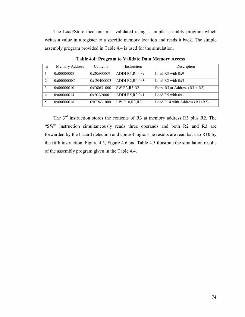
74
The Load/Store mechanism is validated using a simple assembly program which
writes a value in a register to a specific memory location and reads it back. The simple
assembly program provided in Table 4.4 is used for the simulation.
Table 4.4: Program to Validate Data Memory Access
# Memory Address Contents Instruction Description
1 0x00000008 0x20600009 ADDI R3,R0,0x9 Load R3 with 0x9
2 0x0000000C 0x 20400003 ADDI R2,R0,0x3 Load R2 with 0x3
3 0x00000010 0xD8631000 SW R3,R3,R2 Store R3 at Address (R3 + R2)
4 0x00000014 0x20A20001 ADDI R5,R2,0x1 Load R5 with 0x1
5 0x00000018 0xC9431000 LW R10,R3,R2 Load R14 with Address (R3+R2)
The 3rd instruction stores the contents of R3 at memory address R3 plus R2. The
“SW” instruction simultaneously reads three operands and both R2 and R3 are
forwarded by the hazard detection and control logic. The results are read back to R10 by
the fifth instruction. Figure 4.5, Figure 4.6 and Table 4.5 illustrate the simulation results
of the assembly program given in the Table 4.4.

75
Figure 4.5: Load/Store Instructions - Simulation Results (30ns To 130ns) Part I
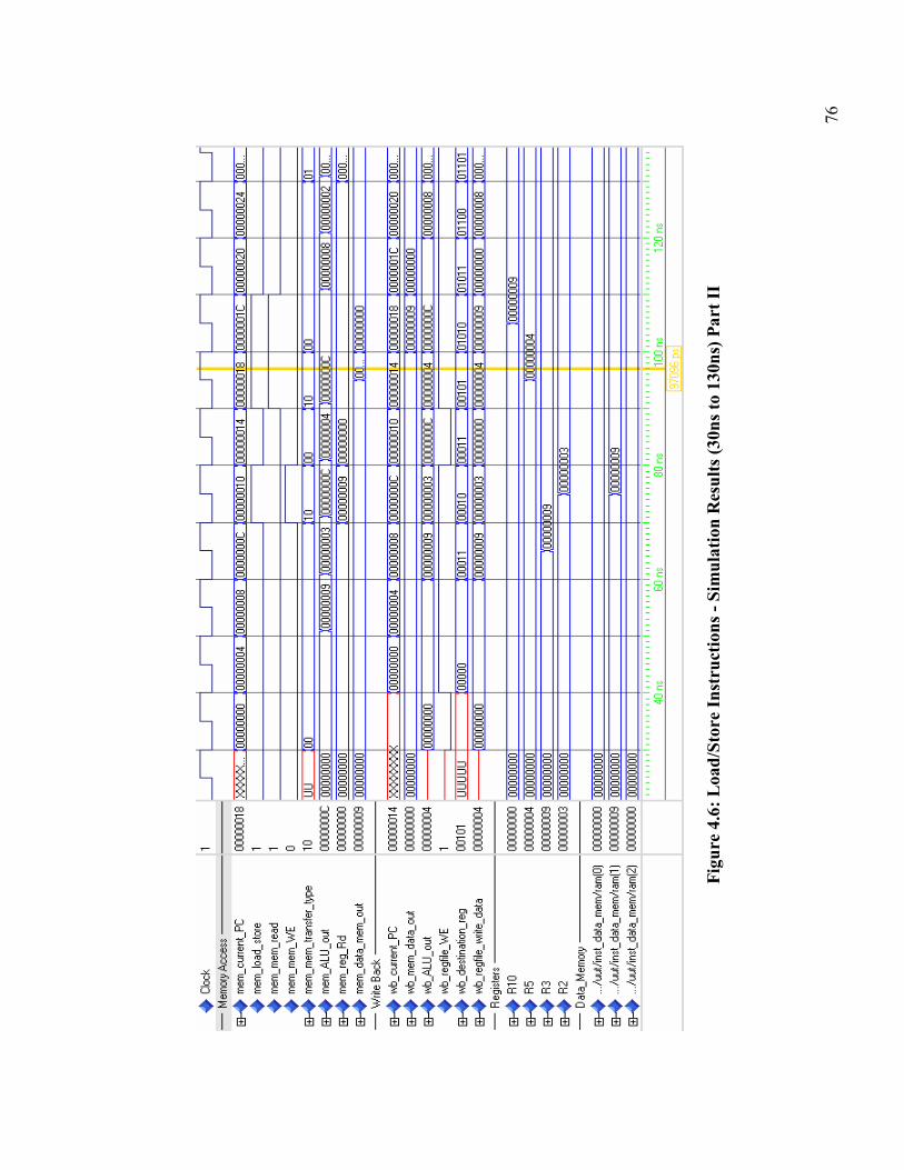
76
Figure 4.6: Load/Store Instructions - Simulation Results (30ns to 130ns) Part II
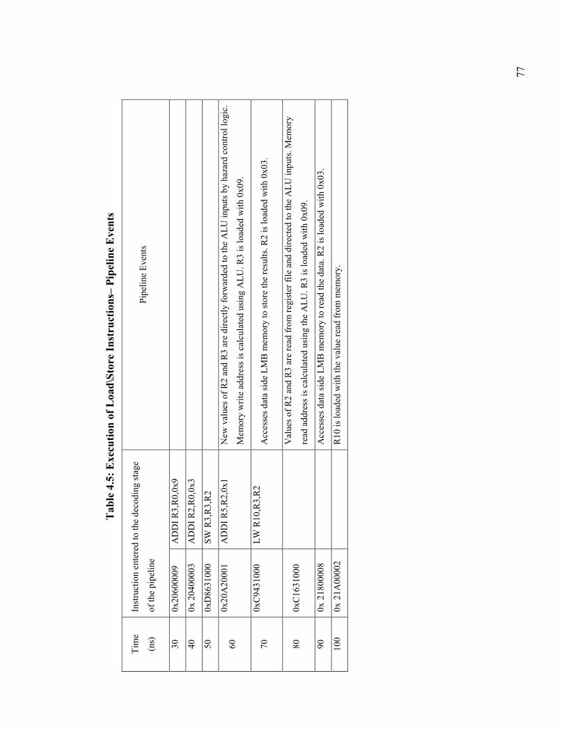
77
Table 4.5: Execution of Load\Store Instructions– Pipeline Events
Tim
e
(ns)
Instruction entered to th
e decoding stage
of th
e pipeline
Pipeline Events
30
0x20
600009
ADDI R3,R0,0x9
40
0x 204
0000
3 ADDI R2,R0,0x3
50
0xD86
31000
SW R3,R3,R2
60
0x20
A20
001
ADDI R5,R2,0x1
New
values of R2 and R3 are directly forwarded to th
e ALU in
puts by hazard control lo
gic.
Mem
ory write add
ress is calculated using ALU. R
3 is lo
aded with 0x09
.
70
0xC94
3100
0 LW R10
,R3,R2
Accesses data side LMB m
emory to store th
e results. R2 is lo
aded with 0x03
.
80
0xC16
3100
0
Values of R2 and R3 are read from register file and directed to th
e ALU in
puts. M
emory
read address is calculated using the ALU. R
3 is lo
aded with 0x09
.
90
0x 218
0000
8
Accesses data side LMB m
emory to read the data. R
2 is lo
aded with 0x03
.
100
0x 21A
0000
2
R10
is lo
aded with the value read from m
emory.
78
4.1.2 RTBlaze Validation
The following setup is used throughout the simulation and validation of the
RTOS feature of RTBlaze.
• CPU runs at 100MHz clock
• One idle task is running (Thread ID zero)
Thread creation, timers, interrupt mechanism and semaphore based synchronization is
verified in this section using simple assembly programs.
4.1.2.1 Timing – Thread Create
The idle thread executes “FORK” instruction to create a new thread. The priority
of the thread is 2, which causes the idle thread to be preempted and the newly created
thread to start executing. The “FORK” instruction has two delay slots which always get
executed. If independent instructions cannot be found, no-operations need to be used.
The simulation results of thread creation assembly code listed in Table 4.6 is illustrated
in Figure 4.7.
Table 4.6: Thread Creation
# Memory Address Contents Instruction Description
1 0x00000050 0x2280006C ADDI R20,R0,0x6c Starting address of the new
thread
2 0x00000054 0x22A00002 ADDI R21,R0,0x2 Priority of the new thread
3 0x00000058 0x5FD5A000 FORK R30,R21,R20 Create a new thread
4 0x0000005C 0x22C00004 FORK delay slot (always
executed)
5 0x00000060 0x22E00003 FORK delay slot (always
executed)
6 0x0000006C 0x21800008 ADDI R12,R0,0x8 First instruction of the new
thread
7 0x00000070 0x 21A00002 ADDI R13,R0,0x2
.
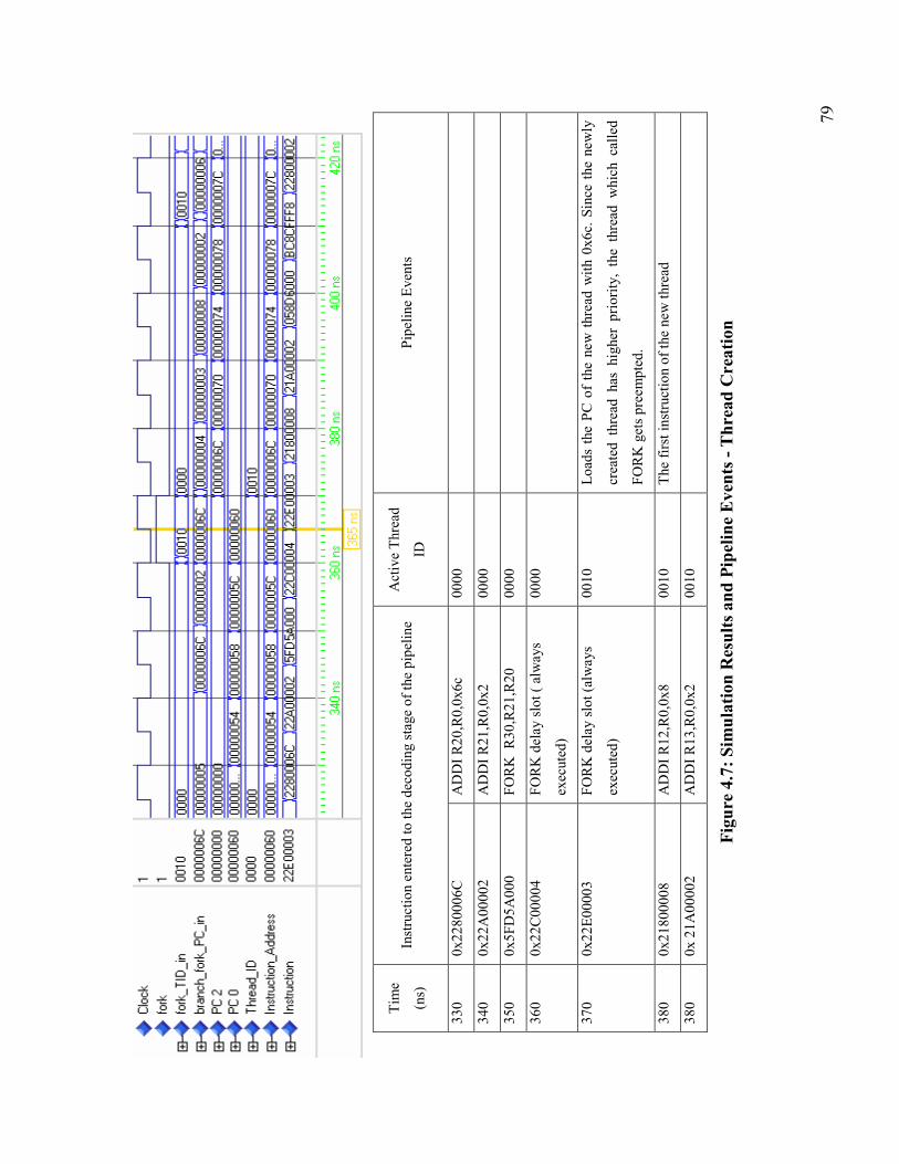
79
Tim
e
(ns)
Instruction entered to th
e decoding stage of the pipeline
Active Thread
ID
Pipeline Events
330
0x22
80006C
ADDI R20
,R0,0x6c
0000
340
0x22
A00
002
ADDI R21
,R0,0x2
0000
350
0x5F
D5A
000
FORK R
30,R21
,R20
00
00
360
0x22
C00
004
FORK delay slot ( always
executed)
0000
370
0x22
E00
003
FORK delay slot (always
executed)
0010
Loads the PC of the new thread with 0x6c. Since the new
ly
created thread has higher priority, the thread w
hich called
FORK gets preempted.
380
0x21
800008
ADDI R12
,R0,0x8
0010
The first in
struction of th
e new th
read
380
0x 21A
0000
2 ADDI R13
,R0,0x2
0010
Figure 4.7: Simulation Results and Pipeline Events - Thread Creation
80
4.1.2.2 Timing - Thread Sleep
The simple assembly code listed in Table 4.7 is used to validate the functionality of
the timers. The thread ID 2 executes the “SLEEP” instruction requesting a 10 cycle
sleep. Upon the execution of the “SLEEP” instruction, the thread ID 0 in the ready
queue resumes the execution for 5 cycles, and is preempted again by the thread ID 2
when the timer expires. Figure 4.8 and Table 4.8 illustrate the simulation results.
Table 4.7: Thread Sleep
# Memory
Address Contents Instruction Description
1 0x0000008C 0x 22A00005 ADDI R21,R0,0x5 Load R21 with 0x5
2 0x00000090 0x 5FD5A280 SLEEP R30,R21 Sleep 5 cycles
3 0x00000094 0x 21C00001 ADDI R14,R0,0x1 Sleep delay slot
4 0x00000098 0x 22A00002 ADDI R21,R0,0x2 Sleep delay slot
5 0x0000009C 0x 5FD5A380 SEMWAIT R30,R21,R20
Idle thread
0x0000006C 22E00003
0x0000008C 23000007
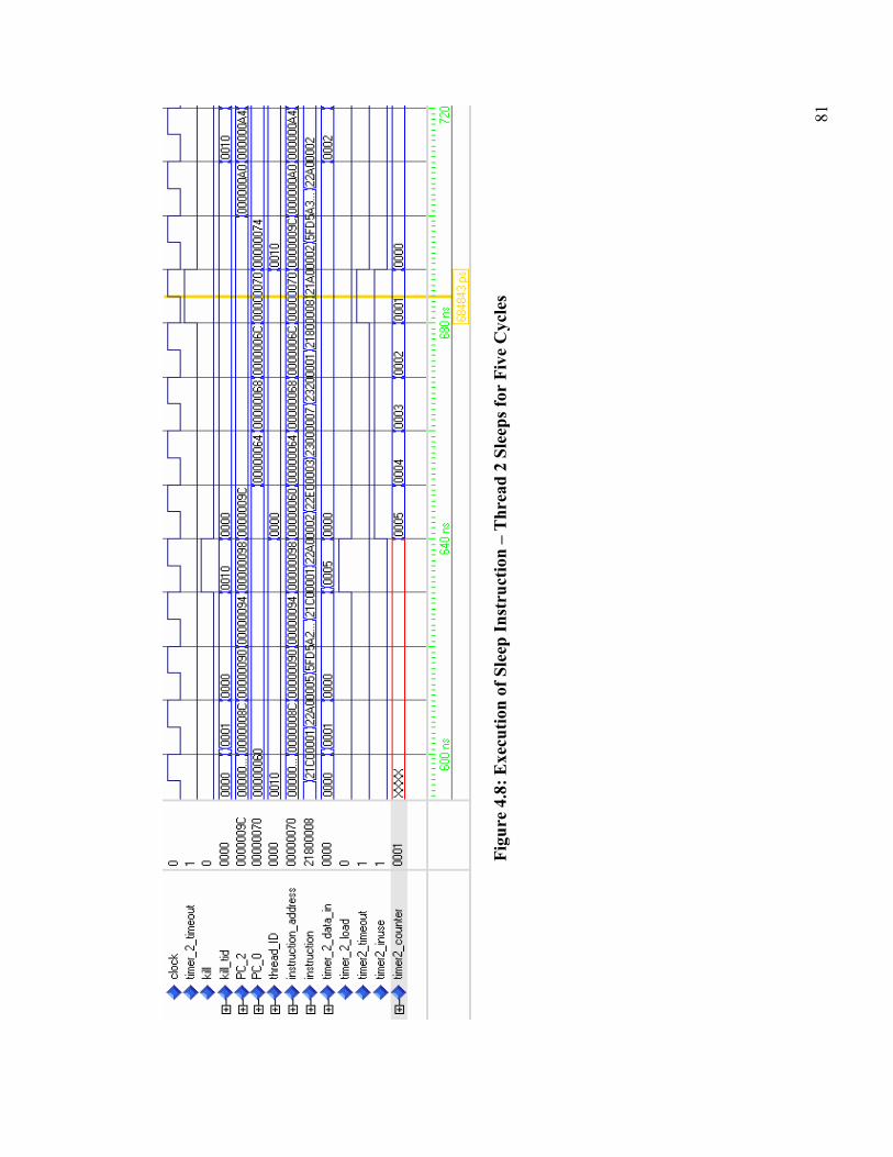
81
Figure 4.8: Execution of Sleep Instruction – Thread 2 Sleeps for Five Cycles
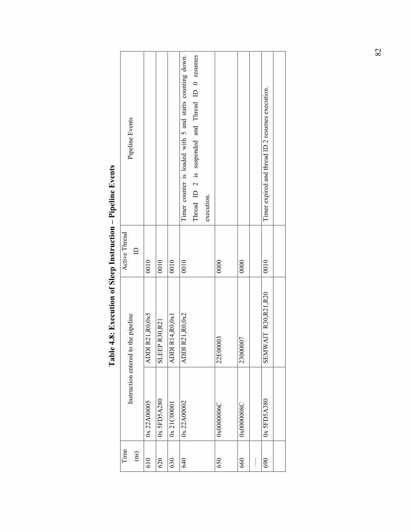
82
Table 4.8: Execution of Sleep Instruction – Pipeline Events
Tim
e
(ns)
Instruction entered to th
e pipeline
Active Thread
ID
Pipeline Events
610
0x 22A
0000
5 ADDI R21
,R0,0x5
0010
620
0x 5FD5A
280
SLEEP R30
,R21
00
10
630
0x 21C
00001
ADDI R14
,R0,0x1
0010
640
0x 22A
0000
2 ADDI R21
,R0,0x2
0010
Tim
er cou
nter is loaded w
ith 5 and starts cou
nting do
wn.
Thread
ID 2
is suspended
and
Thread
ID 0
resumes
execution.
650
0x00
00006C
22
E0000
3 00
00
660
0x00
00008C
23
0000
07
0000
….
690
0x 5FD5A
380
SEMWAIT R
30,R21
,R20
00
10
Tim
er expired and th
read ID 2 resum
es execution
.
83
4.1.2.3 Timing – Interrupt Service Threads
The “IFORK” instruction creates an interrupt service thread. Two delay slots are
used for this instruction. The “ICLEAR” instruction clears the interrupt and prepares the
IST to service the next possible interrupt. The interrupt thread needs to execute the
“ICLEAR” instruction once it services the interrupt. The “ICLEAR” instruction clears
the interrupt bit and reloads the program counter of the IST with the starting address of
the IST. Once the IST executes “ICLEAR”, the idle thread resumes execution. This
instruction has two delay slots.
Table 4.9 lists the assembly code used to create an IST with the priority value of
0xf and to clear the interrupt. Table 4.9 also lists the instructions at the starting address
of the IST. Figure 4.9 illustrates the simulation results of IST creation .The simulation
results in Figure 4.10 shows the activation of the interrupt service thread upon the
occurrence of an external interrupt. As shown in the simulation results (provided that the
IST related to the interrupt is the highest priority thread ready to run) the first instruction
of the IST is scheduled during the next cycle. Figure 4.11 illustrates the simulation
results related to interrupt clear.

84
Table 4.9: A Program to Validate the IST Mechanism
# Memory
Address Contents Instruction Description
1 0x00000050 0x22800074 ADDI R20,R0,0x74 Starting address of the
new IST
2 0x00000054 0x22A0000F ADDI R21,R0,0xF Priority of the new IST
3 0x00000058 0x5FD5A100 IFORK R30,R21,R20 Create a new IST
4 0x0000005C 0x22C00000 Delay slot
5 0x00000060 0x21800008 ADDI R12,R0,0x8 Delay slot
6 0x00000064 0x21A00002 ADDI R13,R0,0x2
7 0x00000068 0x058D6000 RSUB R12,R13,R12
8 0x0000006C 0xBC8CFFF8 BGTI R12,-0x8
Idle loop
# Interrupt Service Thread
1 0x00000074 0x21800008 ADDI R12,R0,0x8
2 0x00000078 0x21A00002 ADDI R13,R0,0x2
3 0x0000007C 0x058D6000 RSUB R12,R13,R12
4 ….
5 …
Service the interrupt.
# IST – Interrupt Clear
1 0x0000008C 0x 22800074 ADDI R20,R0,0x74 Starting address of the IST
2 0x00000088 0x 22A0000F ADDI R21,R0,0xF Priority of the IST
3 0x0000008C 0x 5FD5A200 ICLEAR R30,R21,R20 Clears the interrupt
4 0x00000090 0x 21C00001 ADDI R14,R0,0x1 Sleep delay slot
5 0x00000094 0x 22A00005 ADDI R12,R0,0x8 Sleep delay slot
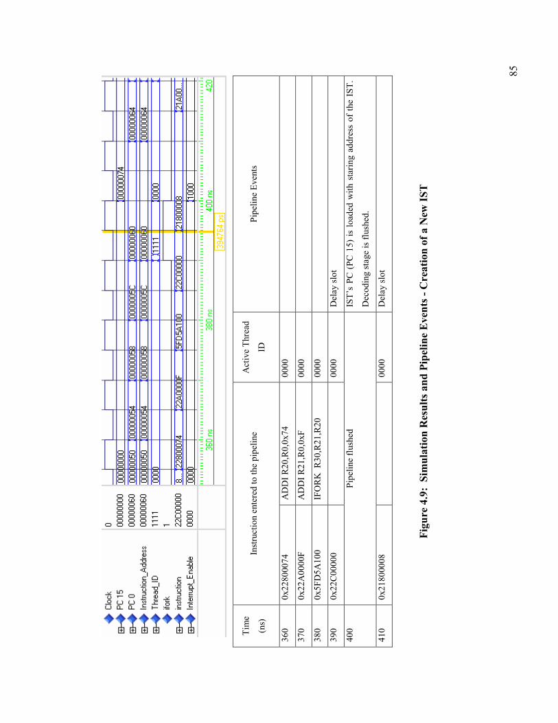
85
Tim
e
(ns)
Instruction entered to th
e pipeline
Active Thread
ID
Pipeline Events
360
0x22
800074
ADDI R20
,R0,0x74
00
00
370
0x22
A00
00F
ADDI R21
,R0,0xF
0000
380
0x5F
D5A
100
IFORK R
30,R21
,R20
00
00
390
0x22
C00
000
00
00
Delay slot
400
Pipeline flushed
IST’s PC (PC 15) is loaded w
ith staring address of the IST.
Decod
ing stage is flushed.
410
0x21
800008
0000
Delay slot
Figure 4.9: Simulation Results and Pipeline Events - Creation of a New
IST
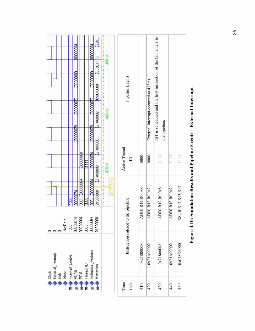
86
Tim
e
(ns)
Instruction entered to th
e pipeline
Active Thread
ID
Pipeline Events
410
0x21
800008
ADDI R12
,R0,0x8
0000
420
0x21
A00
002
ADDI R13
,R0,0x2
0000
External Interrupt occurred at 412
ns.
430
0x21
800008
ADDI R12
,R0,0x8
1111
IST is scheduled and the first instruction of the IST enters to
the pipeline.
440
0x21
A00
002
ADDI R13
,R0,0x2
1111
450
0x05
8D60
00
RSUB R12
,R13
,R12
11
11
Figure 4.10: Simulation Results and Pipeline Events – External Interrupt

87
Tim
e
(ns)
Instruction entered to th
e pipeline
Active Thread
ID
Pipeline Events
620
0x 228
0007
4 ADDI R20
,R0,0x74
11
11
630
0x 22A
0000
F
ADDI R21
,R0,0xF
1111
640
0x 5FD5A
200
ICLEAR R
30,R21
,R20
11
11
650
0x 21C
00001
ADDI R14
,R0,0x1
1111
660
0x 22A
0000
5 ADDI R12
,R0,0x8
1111
Restores
the
starting address
of the
IST. IST finishes
execution and Idle th
read is scheduled to
run.
670
0x05
8D60
00
RSUB R12
,R13
,R12
00
00
Idle th
read resum
es execution.
680
0xBC8C
FFF8
BGTI R12
,-0x8
0000
Figure 4.11: Simulation Results and Pipeline Events – Interrupt Clear

88
4.1.2.4 Timing – Thread Synchronization Using Semaphores
In order to validate the synchronization operations using the semaphore module, a
simple program listed in Table 4.10 is used. The idle thread creates a new thread with
priority value of two. The newly created thread initializes a semaphore to one and
performs wait operation on the semaphore twice. This causes the thread to be blocked on
the semaphore and idle thread to resume execution. Once resumed, idle thread performs a
post operation on the semaphore which results in unblocking the TID 0x2. Figure 4.12,
Figure 4.13 and Table 4.11 show the simulation results.
Table 4.10: A Program to Validate Semaphore Operations
# Memory
Address Contents Instruction Description
1 0x0000008C 0x 22800002 ADDI R20,R0,0x2 Semaphore ID = 0x02
2 0x00000090 0x 22A00001 ADDI R21,R0,0x1 Semaphore value = 0x01
3 0x00000094 0x 5FD5A300 SEMINIT R30,R21,R20 Creates the semaphore
4 0x00000098 0x 21C00001
5 0x0000009C 0x 22A00002 ADDI R21,R0,0x2
6 0x000000A0 0x 5FD5A380 SEMWAIT R30,R21,R20 TID 0x2 waits on semaphore
7 0x000000A4 0x 22A00002 ADDI R21,R0,0x1
8 0x000000A8 0x 22A00002 ADDI R21,R0,0x1
9 0x000000AC 0x 22800002 ADDI R20,R0,0x2
10 0x000000B0 0x 22A00002 ADDI R21,R0,0x2
11 0x000000B4 0x 5FD5A380 SEMWAIT R30,R21,R20 TID 0x2 waits on semaphore
12 0x000000B8 0x 22A00002 ADDI R21,R0,0x2
13 0x000000BC 0x 22A00003 ADDI R21,R0,0x3
14 0x000000C0 0x 22A00004 ADDI R21,R0,0x4
15 0x000000C4 0x 22A00005 ADDI R21,R0,0x5
Thread ID 0x00
16 0x00000060 0x 22800002 ADDI R20,R0,0x2
17 0x00000064 0x 22A00002 ADDI R21,R0,0x2
18 0x00000068 0x 5FD5A400 SEMPOST R30,R20 Signals the semaphore
19 0x0000006C 0x 22A00003 ADDI R21,R0,0x3
20 0x00000070 0x 22A00005 ADDI R21,R0,0x5
21 0x00000074 0x 22A00005 ADDI R21,R0,0x5
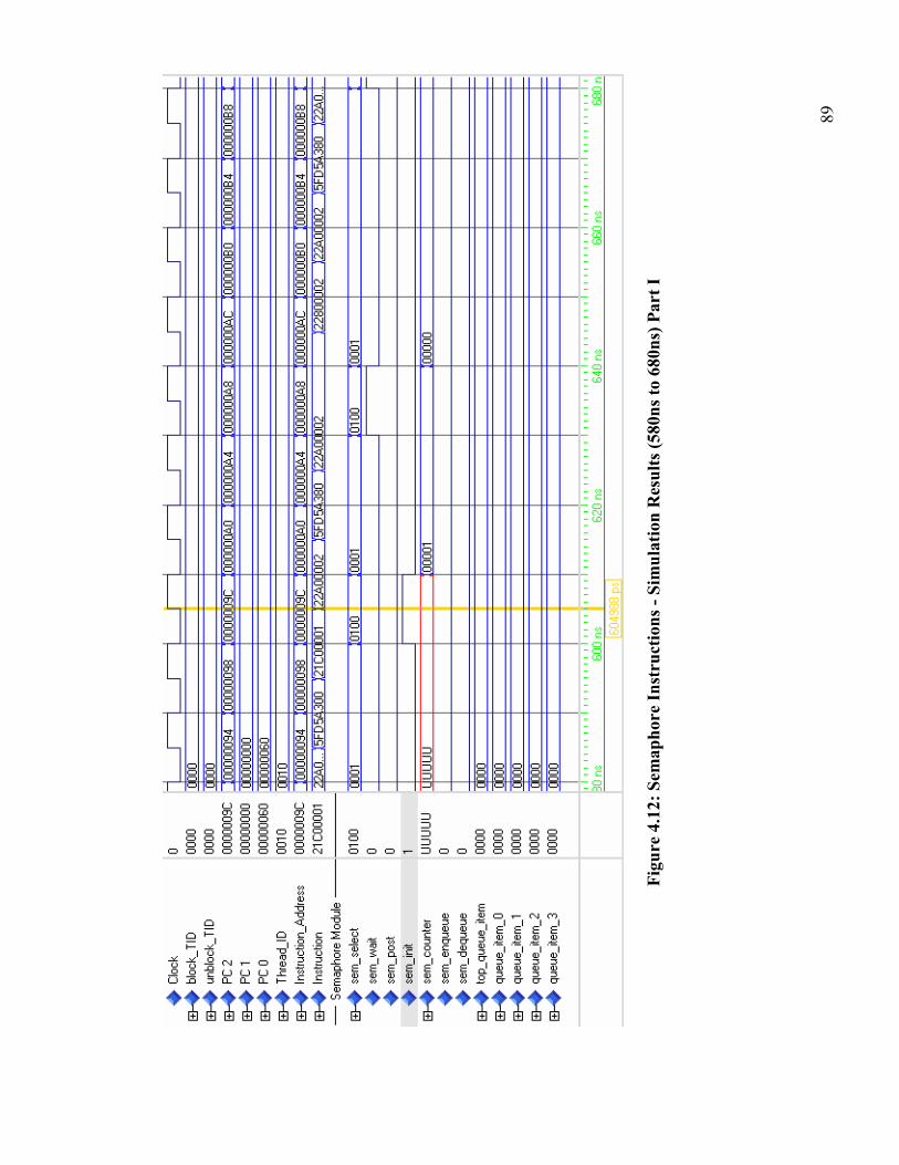
89
Figure 4.12: Semaphore Instructions - Simulation Results (580ns to 680ns) Part I

90
Figure 4.13: Semaphore Instructions - Simulation Results (680ns to 780ns) Part II
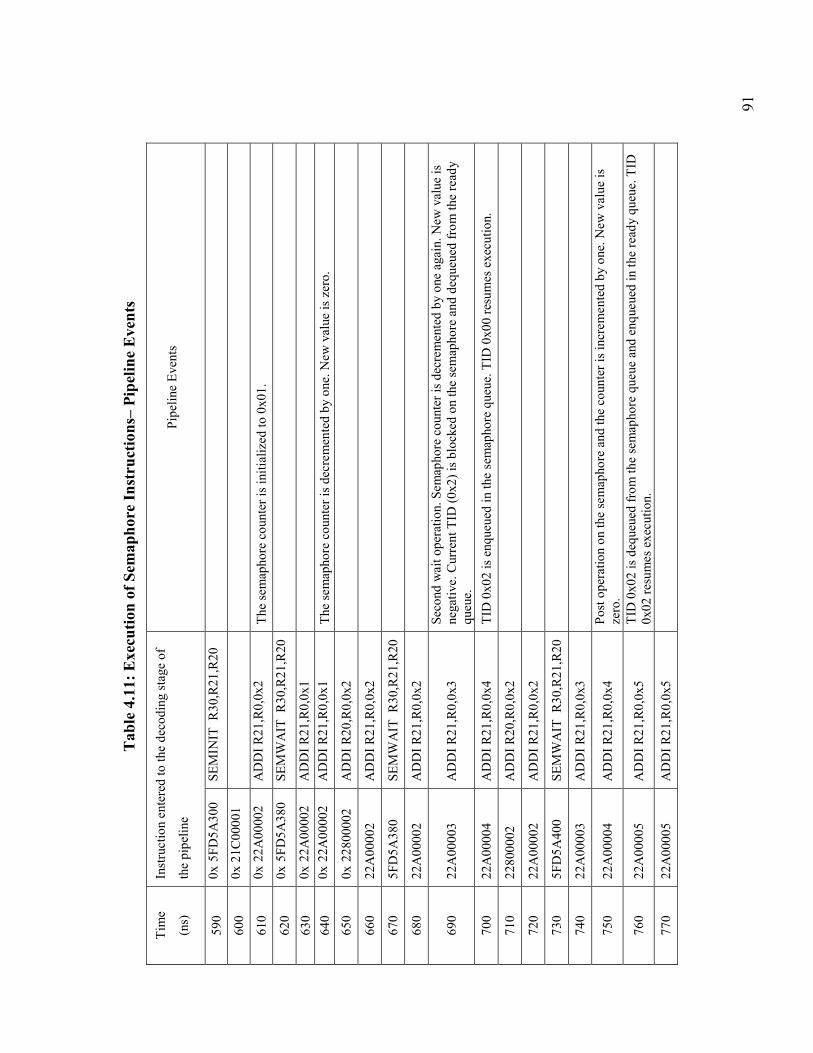
91
Table 4.11: Execution of Sem
aphore Instructions– Pipeline Events
Tim
e
(ns)
Instruction entered to th
e decoding stage of
the pipeline
Pipeline Events
590
0x 5FD5A
300
SEMIN
IT R
30,R21
,R20
600
0x 21C
00001
610
0x 22A
0000
2 ADDI R21
,R0,0x2
The sem
aphore counter is in
itialized to 0x01.
620
0x 5FD5A
380
SEMWAIT R
30,R21
,R20
630
0x 22A
0000
2 ADDI R21
,R0,0x1
640
0x 22A
0000
2 ADDI R21
,R0,0x1
The sem
aphore counter is decremented by one. N
ew value is zero.
650
0x 228
0000
2 ADDI R20
,R0,0x2
660
22A00
002
ADDI R21
,R0,0x2
670
5FD5A
380
SEMWAIT R
30,R21
,R20
680
22A00
002
ADDI R21
,R0,0x2
690
22A00
003
ADDI R21
,R0,0x3
Second wait o
peration. S
emaphore counter is decremented by one again. N
ew value is
negative. C
urrent TID
(0x2) is blocked on the semaphore and
dequeued from
the ready
queue.
700
22A00
004
ADDI R21
,R0,0x4
TID
0x02 is enqueued in th
e semaphore queue. T
ID 0x00 resumes execution.
710
228000
02
ADDI R20
,R0,0x2
720
22A00
002
ADDI R21
,R0,0x2
730
5FD5A
400
SEMWAIT R
30,R21
,R20
740
22A00
003
ADDI R21
,R0,0x3
750
22A00
004
ADDI R21
,R0,0x4
Post o
peratio
n on th
e semapho
re and th
e counter is in
crem
ented by one. N
ew value is
zero.
760
22A00
005
ADDI R21
,R0,0x5
TID
0x02 is dequeued from
the semaphore queue and enq
ueued in th
e ready queue. TID
0x02
resum
es execution.
770
22A00
005
ADDI R21
,R0,0x5
92
4.2 Performance Comparison
In order to evaluate the performance of RTBlaze, a comparison with software
RTOSs needs to be carried out. Ronnholm [62] has evaluated three software RTOSs for
Xilinx MicroBlaze processor. Xilkernal, Asterix and uClinux are selected for the
comparison. The results related to those OSs are investigated in this section and
compared with the RTBlaze simulation results.
uClinux [63] is a lightweight version of the standard Linux kernel [64], targeting
microcontrollers. The main difference is that uClinux does not support virtual memory.
The development is done by the standard GNU tool chain used for Linux. The
scheduling model is the same as that of Linux and supports three scheduling policies:
round robin, First-In First-Out (FIFO) and slandered time sharing.
Asterix [65] is a research grade open-source RTOS developed by the Malardalen
Real-Time Research Center at Malardalen University. A separate configuration tool is
used to configure the kernel parameters such as system clock resolution and TCB list.
EDK compiler tools can be used for the Asterix based application software development.
The kernel supports static priority preemptive scheduling as well as an event triggered
mode of operation. The interrupt handling architecture has two levels which are the same
as Xilkernal.
Xilkernal [39] is an open source small footprint robust software RTOS that comes
with the Xilinx EDK tool chain. Xilkernal provides a POSIX like interface with the
ability to handle semaphores, interrupts, mutexes and message queues. Modularity of the
kernel allows configurability of these modules. As a result, the kernel can be tailored for
the specific needs of the given application. Xilkernal supports both priority-based
preemptive scheduling and round robin scheduling. The policy is global and needs to be
initialized at configuration time of the kernel.
The SoPC used for the evaluation of the RTOSs are minimalist and only include
the IP components required to implement minimalist Microblaze based SoPC running
the RTOSs [62]. The SoPC system includes the following.
• 100 MH system clock
• 64 MB DDR ram
93
• 16 KB L1 I-cache
• 16 KB L1 D-cache
• OPB timer [66]
The software setup is also simple and Xilkernal and Asterix have only one task running
(the idle task). uClinux have seven system tasks running. The evaluation is based on
interrupt latency and task response time. Interrupt latency is the number of clock cycles
the kernel takes to start executing the interrupt handling routing once an external
interrupt occurs. The benchmarking is done by generating a periodic external interrupt
using the OPB timer and reading the timer counter register at the beginning of the ISR to
find out the cycles the kernel consumed in order to reach the ISR. The task response
time, the time the kernel takes to reschedule the next highest priority task from the
occurrence of an external interrupt, is also measured using a similar manner. This
measurement is a fair estimation of the scheduler overhead.
4.2.1 Comparison of the Performance of RTBlaze and Software RTOSs
The simulation environment used to validate RTBlaze is almost similar to the
setup used to evaluate the RTOSs for Microblaze. Ronnholm’s [62] evaluation of
RTOSs for MicroBlaze uses two configurations: cache enabled and cache disabled for
benchmarks. RTBlaze is a cacheless CPU which targets real-time systems based on
SoPC based systems. The program memory is supposed to be on chip block RAM which
runs at full CPU speed. The memory access of RTBlaze is equivalent to the Microblaze
system with cache enabled since all the benchmark code resides in the cache [62]. This
makes the comparison between the Microblaze processor with cache enabled benchmark
results [62] and RTBlaze simulation results reasonable. Table 4.12 summarizes the
comparison results of the interrupt latency and task response time.

94
Table 4.12: Latencies
RTOS Interrupt Latency
Cycles(Time)
Task Response Time
Cycles(Time)
uClinux 5630(56.3uS) 22441(224.4uS)
Xilkernal 564 (5.64uS) 2590(25.90uS)
Asterix 494(4.94uS) 2508 (25.08uS)
RTBlaze 5 (50nS) 5(50nS)
As shown in the simulation results in Section 4.1, RTBlaze completely removes
the RTOS overhead because of the hardware migration of the components of the RTOS.
Upon an external interrupt, given that the IST is the highest priority ready thread, the
IST is scheduled in the next CPU cycle. Obviously, RTBlaze has zero scheduler
overhead, where the return from the interrupt service thread causes the next highest
priority thread to be scheduled in the next CPU cycle.
4.3 Size of the Kernel Footprint
When it comes to RTOSs, the kernel size is a very important factor. RTBlaze does
not need any software code for the kernel operation as it implements the primitive OS
level functionality directly in hardware. Comparison results of the kernel footprints of
the RTOSs are given in Table 4.13.
Table 4.13: Kernel Footprint Comparison
RTOS Kernel Footprint
uClinux 1.759 MB
Asterix 7.70 kB
Xilkernal (minimalist) 19.97 kB
RTBlaze 0kB

95
4.4 Analysis of Area Overhead
The chip utilization of FPGAs is measured using the number of FPGA logic
resources being used. In order to analyze the area overhead, the LUT and flip flop count
are usually used. Removal of OS overhead comes at the increased utilization of the chip
area, and this overhead is measured using LUTs and flip flops. This section analyzes the
chip area utilization of the real-time extensions in comparison with Microblaze processor
and the multithreaded base processor.
Currently, the base processor implements a subset of the Microblaze processor
instruction set. This includes the instruction set of a minimalist Microblaze processor.
The configuration of the RTBlaze used for this comparison has the following features.
• 16 threads
• 4 interrupt service threads
• 15 timers
• 4 semaphores each with 4-element deep wait queue
Table 4.14 shows the comparison results of Microblaze, multithreaded base
processor and RTBlaze.
Table 4.14: Resource Utilization Of RTOS Extensions
LUTs Slice Flip Flops Block RAMs
Microblaze (Minimalist) 975 485 0
Base processor 674 309 0
RTBlaze 1652 712 3
Real-time extensions have resulted in almost doubling the area of the base
processor. The resource usage of the base processor is lower than the Xilinx MicroBlaze
processor with minimalist configuration. This is due to the fact that the prototype base
processor does not implement all the bus interfaces that come with the Microblaze
processor. Table 4.15 further analyzes the breakdown of the resource usage due to the
RTOS extension.
96
Table 4.15: Breakdown of Area Overhead Due to RTOS Extensions
RTOS Component LUTs Slice Flip Flops
Scheduler and PC
counter bank
15.5 % 4.9 %
Semaphore module 41.6 % 27.7 %
Timer module 39.7 % 67.4 %
Other 3.2 % 0%
The timer module has the highest overall resource usage. The next highest
resources usage is due to the addition of the semaphore module. The resource
requirement of the scheduler is under 20%. Other resources include the control unit
modification in order to support RTOS instructions and the data path modifications due
to the attachment of RTOS components.
97
Chapter 5
Conclusions and Future Work
5.1 Conclusions
Real-time operating systems with conventional processors are widely used in the
context of embedded computing. The overhead due to the software kernel contributes to
the degradation the overall performance of RTOS based embedded systems. Previous
research efforts focusing on migrating the RTOS functionality into hardware provide
promising results. Multithreaded processors are a distinct area of research targeted to
exploit thread level parallelism by interleaving multiple threads at the hardware level.
The concept of multithreading can easily be extended to achieve a zero overhead context
switching mechanism and fast interrupt service mechanism. Based on earlier research
efforts, this thesis proposes a new multithreaded softcore processor, RTBlaze, with
hardware RTOS support in order to eliminate the overhead due to software.

98
The attachment of the hardware migrated RTOS components to a multithreaded
processor gives various advantages over the IP based separate migration approach. Use
of the multithreaded processor as the base processor gives the ability of zero overhead
context switching with the ability of implementing zero latency ISTs. The tight coupling
of a hardware migrated scheduler completely removes the scheduler overhead. The
scheduler works cooperatively with the hardware implemented semaphore module in
order to realize a blocking synchronization scheme with zero overhead. Timers are also
implemented in hardware and completely remove the overhead and provide timing with
very high resolution. Unlike implementations of RTOS as separate chips, tightly
coupling the RTOS functionality to the processor pipeline reduces the interfacing glue
logic and nondeterminism occurs in system calls due to nondeterministic bus arbitration
schemes. Not only the zero overhead OS level functionality, but RTBlaze owns one key
feature, the zero size kernel. This leaves enough room to have all the application code in
the on-chip memory. Current FPGA technology integrates more and more on chip
memory enabling multiple RTBlazes to work in parallel with no external memory and
cache.
The Vertex family is targeted for the prototype implementation of RTBlaze. The
processor runs at 119 MHz of clock speed with hardware level support for 16 threads, 4
ISTs, 4 semaphores and 15 timers. RTBlaze outperforms conventional software RTOSs
by providing interrupts and scheduling latencies as low as 50 ns.
Migration and attachment of RTOS functionality to the processor substantially
increase the area required to synthesis the RTBlaze processor. For the current prototype,
the RTOS extension has almost doubled the base processor size. When it comes to the
RTBlaze based SoPC systems, the RTBlaze processor reduces the area required to
implement the system by reducing the number of IPs required. Multiple numbers of
external interrupt lines eliminate the need of an external interrupt controller. EDK based
SoPC uses timer IP to provide timer interrupt while RTBlaze eliminates this while
providing high resolution timing. Apart from that, the area required to implement the
cache controllers for both processors, the cache coherency mechanism and off chip
memory controller is substantial.

99
When it comes to the real application domains, fast interrupt service threads, a
zero overhead synchronization mechanism with high resolution timers simplify the
external interface design. For example, the sampling subsystem of the digital control
systems can be easily and efficiently implemented using these resources. Unlike
software based RTOSs, the high resolution timers with zero overhead interrupts make it
possible to implement real-time digital controllers with very high sampling rates. Apart
from that, the software solution to implement communication interfaces such as RS232,
SPI, etc. results in reducing the number of IP cores required in SoPC based system.
5.2 Future Work
RTBlaze is a basic prototype level implementation and needs several
improvements. Most critical improvements identified are as follows.
• Implementation and verification of the complete instruction set
• Implementation of bus interfaces such as OPB and PLB
• Implementation of exception handling threads
• Extension of the scheduler to support round robin scheduling policy
• Addition of a mechanism to address priority inversion
• Addition of configurability through a front-end configuration tool
• Extension of the GNU GCC backend to support RTOS instructions
The above improvements would allow seamless integration with EDK tool chain
and design of complete SoPC systems using EDK library IPs. The delay slots can be
filled with independent instructions from the thread by moving it down. This
optimization can be automated by retargeting the GCC backend.
Further optimizations to the RTBlaze are also possible,
• Implement an EDF like scheduler
• More efficient mapping of FPGA resources and full structural level design
of RTBlaze
100
New scheduling algorithms can also be explored by combining conventional process
scheduling algorithms with the cycle or block interleaved multithreading facility of the
RTBlaze.
Multiprocessor systems with distributed hardware RTOS nodes can be built using
an array of RTBlaze processors. EDK already has support for multiprocessor designs, so
this can be easily designed using the Xilinx tool chain. To enable multiprocessor
support, an inter-processor synchronization mechanism needs to be introduced to
synchronize inter-processor level threads.
101
References
[1] L. Lindh, "FASTHARD - A Fast Time Deterministic HARDware Based Real-
time Kernel," in Proceedings of the Fourth Euromicro workshop on Real-Time
Systems: IEEE, 1992, pp. 21 - 25, ISBN: 0-8186-2815-4.
[2] T. Nakano, A. Utama, M. Itabashi, A. Shiomi, and M. Imai, "Hardware
implementation of a real-time operating system," in Proceedings of the 12th
TRON Project International Symposium Washington, DC, USA: IEEE Computer
Society 1995, pp. 34, ISBN:0-8186-7207-2.
[3] D. Niehaus, K. Ramamritham, J. A. Stankovic, G. Wallace, C. Weems, W.
Burleson, and J. Ko, "The Spring scheduling co-processor: Design, use, and
performance," in Proceedings of the Real-Time Systems Symposium Raleigh
Durham, NC, USA: IEEE, 1993, pp. 106-111, ISBN: 0-8186-4480-X.
[4] P. Kohout, B. Ganesh, and B. Jacob, "Hardware support for real-time operating
systems," in International Symposium on Systems Synthesis, Proceedings of the
1st IEEE/ACM/IFIP international conference on Hardware/software codesign
and system synthesis Newport Beach, CA, USA: ACM, 2003, pp. 45 - 51,
ISBN:1-58113-742-7.
[5] J. Hildebrandt, F. Golatowski, and D. Timmermann, "Scheduling coprocessor for
enhanced least-laxity-first schedulingin hard real-time systems," in Proceedings
of the 11th Euromicro Conference on Real-Time Systems York, UK: IEEE, 1999,
pp. 208-215, ISBN: 0-7695-0240-7.
[6] S. Saez, J. Vila, A. Crespo, and A. Garcia, "A hardware scheduler for complex
real-time systems," in Proceedings of the IEEE International Symposium on
Industrial Electronics. ISIE Bled, Slovenia: IEEE, 1999, pp. 43-48, ISBN: 0-
7803-5662-4.
[7] J. Hildebrandt and D. Timmermann, "An FPGA based Scheduling Coprocessor
for Dynamic Priority Scheduling in Hard Real-Time Systems," in Field-
102
Programmable Logic and Applications: The Roadmap to Reconfigurable
Computing: SpringerLink, 2000, pp. 777-780, ISBN 978-3-540-67899-1.
[8] P. Kuacharoen, M. A. Shalan, and V. J. M. Iii, "A configurable hardware
scheduler for real-time systems," in Proceedings of the International Conference
on Engineering of Reconfigurable Systems and Algorithms: CSREA Press, 2003,
pp. 96-101.
[9] L. Lindh and F. Stanischewski, "FASTCHART-Idea and Implementation," in
Proceedings of the IEEE International Conference on Computer Design on VLSI
in Computer & Processor Washington, DC, USA: IEEE Computer Society,
1991, pp. 401-404, ISBN:0-8186-2270-9.
[10] T. Ungerer, B. Robič, and J. Šilc, "A survey of processors with explicit
multithreading," in ACM Computing Surveys New York, NY, USA, 2003, pp.
29-63, ISSN:0360-0300.
[11] U. Brinkschulte, C. Krakowski, C. Kreuzinger, and T. Ungerer, Interrupt service
threads - a new approach to handle multiple hard real-time events on a
multithreaded microcontroller: RTSS WIP sessions, 1999.
[12] U. Brinkschulte, C. Krakowski, J. Kreuzinger, and T. Ungerer, "A Multithreaded
Java Microcontroller for Thread-Oriented Real-Time Event Handling," in
Proceedings of the International Conference on Parallel Architectures and
Compilation Techniques Washington, DC, USA: IEEE Computer Society, 1999,
pp. 34, ISBN:0-7695-0425-6.
[13] J. Kreuzinger, R. Marston, T. Ungerer, U. Brinkschulte, and C. krakowski, "The
komodo project: thread-based event handling supported by a multithreaded java
microcontroller," in 25th EUROMICRO Conference Milan, Italy, 1999, pp. 122-
128.
[14] M. Pfeffer, S. Uhrig, T. Ungerer, and U. Brinkschulte, "A Real-Time Java
System on a Multithreaded Java Microcontroller," in Proceedings of the Fifth
IEEE International Symposium on Object-Oriented Real-Time Distributed
Computing: IEEE Computer Society, 2002, pp. 34, ISBN:0-7695-1558-4.
103
[15] "MicroBlaze Processor Reference Guide, EDK 9.1i, Xilinx product
specification," Xilinx,
www.xilinx.com/support/documentation/sw_manuals/mb_ref_guide.pdf.
[16] "Virtex-II Pro and Virtex-II Pro X Platform FPGAs: Complete Data Sheet":
Xilinx, www.xilinx.com/support/documentation/user_guides/ug012.pdf.
[17] "EDK Concepts, Tools, and Techniques, EDK 9.1i," Xilinx, EDK 9.1i.
[18] V. Asokan, Designing Multiprocessor Systems in Platform Studio: Xilinx,
www.xilinx.com/support/documentation/white_papers/wp262.pdf
[19] M. Hübner, K. Paulsson, and J. Becker, "Parallel and Flexible Multiprocessor
System-On-Chip for Adaptive Automotive Applications based on Xilinx
MicroBlaze Soft-Cores " in 19th IEEE International Parallel and Distributed
Processing Symposium, 2005, pp. 149, ISBN:1530-2075.
[20] "Intel® PXA270 Processor : Data Sheet," intel,
www.intel.com/design/embeddedpca/applicationsprocessors/302302.htm.
[21] "AMBA™ Specification, Rev 2.0," Arm,
www.arm.com/products/solutions/AMBA_Spec.htm.
[22] "CoreConnect Bus Architecture, 32-, 64-, 128-bit core on-chip bus standard,"
IBM, http://www-
01.ibm.com/chips/techlib/techlib.nsf/literature/CoreConnect_Bus_Architecture.
[23] "WISHBONE System-On-Chip (SoC) Interconnection Architecture for Portable
IP Cores," OpenCores, www.opencores.org/projects.cgi/web/wishbone/.
[24] "Processor Local Bus (PLB) v3.4 (v1.02a)": Xilinx,
www.xilinx.com/support/documentation/ip_documentation/plb_v34.pdf, 2006.
[25] "On-Chip peripheral Bus V2.0 with OPB Arbiter": Xilinx,
www.xilinx.com/support/documentation/ipembedprocess_coreconnect_opbbusstr
uct.htm.
[26] "ISE In-Depth Tutorial": Xilinx,
www.download.xilinx.com/direct/ise9_tutorials/ise9tut.pdf, 2007.
[27] Development System Reference Guide, Xilinx ISE 9.1i: Xilinx,
www.toolbox.xilinx.com/docsan/xilinx9/books/docs/dev/dev.pdf.
104
[28] R. Ernst, "Codesign of embedded systems: status and trends," IEEE Design &
Test of Computers, pp. 45-54, 1998.
[29] "Microprocessor Debug Module (MDM) (v2.00a)": Xilinx,
www.china.xilinx.com/support/documentation/ip_documentation/mdm.pdf.
[30] M. Hübner and J. Becker, "Exploiting Dynamic and Partial Reconfiguration for
FPGAs — Toolflow, Architecture and System Integration," in Proceedings of the
19th annual symposium on Integrated circuits and systems design: ACM, 2006,
pp. 1-4, ISBN:1-59593-479-0.
[31] "Two Flows for Partial Reconfiguration: Module Based or Difference Based,"
Xilinx, www.xilinx.com/support/documentation/application_notes/xapp290.pdf.
[32] "Local Memory Bus (LMB) V1.0," Xilinx,
www.china.xilinx.com/support/documentation/ip_documentation/lmb.pdf.
[33] "LMB BRAM Interface Controller v2.00a," Xilinx,
www.china.xilinx.com/support/documentation/ip_documentation/lmb_bram_if_c
ntlr.pdf.
[34] "Block RAM (BRAM) Block," Xilinx,
www.xilinx.com/support/documentation/ip_documentation/bram_block.pdf.
[35] "Fast Simplex Link (FSL) Bus v2.10a," Xilinx,
www.china.xilinx.com/support/documentation/ip_documentation/fsl_v20.pdf.
[36] A. Silberschatz, P. B. Galvin, and G. Gagne, Operating System Concepts, 7th
Edition ed., 2007.
[37] A. Mohammadi and S. G. Akl, "Scheduling Algorithms for Real-Time Systems,"
School of Computing Queen’s University Kingston, Ontario Canada,
www.cs.queensu.ca/home/akl/techreports/scheduling.pdf2005.
[38] A. Burns, "Scheduling hard real-time systems: a review " Software Engineering,
www.cse.ucsc.edu/~sbrandt/courses/Winter00/290S/burns.pdf 1991.
[39] "OS and Libraries Document Collection, EDK 9.1i, 2006," Xilinx,
www.xilinx.com/support/documentation/sw_manuals/edk10_oslib_rm.pdf.
[40] J. L. Hennessy and D. A. P. A. C. Arpaci-Dusseau, Computer Architecture: A
Quantitative Approach, 4th Edition ed., 2007.
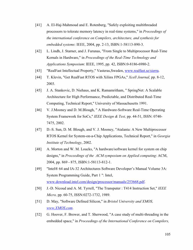
105
[41] A. El-Haj-Mahmoud and E. Rotenberg, "Safely exploiting multithreaded
processors to tolerate memory latency in real-time systems," in Proceedings of
the international conference on Compilers, architecture, and synthesis for
embedded systems: IEEE, 2004, pp. 2-13, ISBN:1-58113-890-3.
[42] L. Lindh, J. Starner, and J. Furunas, "From Single to Multiprocessor Real-Time
Kernals in Hardware," in Proceedings of the Real-Time Technology and
Applications Symposium: IEEE, 1995, pp. 42, ISBN:0-8186-6980-2.
[43] "RealFast Intellectual Property," Vasteras,Sweden, www.realfast.se/sierra.
[44] T. Klevin, "Get RealFast RTOS with Xilinx FPGAs," Xcell Journal, pp. 8-12,
2003.
[45] J. A. Stankovic, D. Niehaus, and K. Ramamritham, " SpringNet: A Scalable
Architecture for High Performance, Predictable, and Distributed Real-Time
Computing, Technical Report," University of Massachusetts 1991.
[46] V. J.Mooney and D. M.Blough, " A Hardware-Software Real-Time Operating
System Framework for SoCs," IEEE Design & Test, pp. 44-51, ISSN: 0740-
7475, 2002.
[47] D.-S. Sun, D. M. Blough, and V. J. Mooney, "Atalanta: A New Multiprocessor
RTOS Kernel for System-on-a-Chip Applications, Technical Report," in Georgia
Institute of Technology, 2002.
[48] A. Morton and W. M. Loucks, "A hardware/software kernel for system on chip
designs," in Proceedings of the ACM symposium on Applied computing: ACM,
2004, pp. 869 - 875, ISBN:1-58113-812-1.
[49] "Intel® 64 and IA-32 Architectures Software Developer’s Manual Volume 3A:
System Programming Guide, Part 1 ": Intel,
www.download.intel.com/design/processor/manuals/253668.pdf.
[50] J.-D. Nicoud and A. M. Tyrrell, "The Transputer : T414 Instruction Set," IEEE
Micro, pp. 60-75, ISSN:0272-1732, 1989.
[51] D. May, "Software Defined Silicon," in Bristol University and XMOS,
www.XMOS.com.
[52] G. Hoover, F. Brewer, and T. Sherwood, "A case study of multi-threading in the
embedded space," in Proceedings of the International Conference on Compilers,
106
Architecture and Synthesis for Embedded Systems: ACM, 2006, pp. 357-367,
ISBN:1-59593-543-6.
[53] K. Tanaka, "PRESTOR-1: A Processor Extending Multithreaded Architecture,"
in Innovative Architecture for Future Generation High-Performance Processors
and Systems: IEEE, 2005, pp. 8, ISSN: 1527-1366, ISBN: 0-7695-2483-4.
[54] K. Tanaka, "Real-Time Operating System Kernel for Multithreaded Processor,"
in Proceedings of the International Workshop on Innovative Architecture for
Future Generation High Performance Processors and Systems, IEEE: IEEE
Computer Society, 2006, pp. 91-100.
[55] M. Schoeberl, "A Java processor architecture for embedded real-time systems,"
Journal of Systems Architecture: the EUROMICRO Journal, pp. 265-286,
ISSN:1383-7621, 2003.
[56] "Xilkernel, EDK 9.1i, Xilinx product specification," Xilinx, EDK 9.1i.
[57] P. Glover, "Using and Creating Interrupt-Based Systems," Application Note:
Embedded Hardware Systems, Xilinx,
www.xilinx.com/support/documentation/application_notes/xapp778.pdf
[58] "Using Block RAM in Spartan-3 Generation FPGAs," Application Note, Xilinx,
www.xilinx.com/support/documentation/application_notes/xapp463.pdf.
[59] J. P. Bradford and S. Abraham, "Efficient Synchronization for Multithreaded
Processors," http://citeseerx.ist.psu.edu/viewdoc/summary?doi=10.1.1.56.6592.
[60] B. K. Kim and K. G. Shin, "Scalable hardware earliest-deadline-first scheduler
for ATM switching networks," in 18th IEEE Real-Time Systems Symposium
(RTSS '97), 1997, pp. 210, ISBN:0-8186-8268-X.
[61] B. M. Al-Hashimi, System-on-Chip: Next Generation Electronics (Circuits,
Devices and Systems) 2006.
[62] A. Ronnholm, "Evaluation of Real-Time Operating Systems for Xilinx
MicroBlaze CPU, Thesis," in Computer Science and Electronics: Malardalens
University, 2006.
[63] "Embedded Linux/Microcontroller Project," http://www.uclinux.org/.
[64] D.P.Bovet and M. Cesati, Understanding the LINUX KERNAL: O'Reilly, 2003.

107
[65] H. Thane, A. Pettersson, and D. Sundmark, "The asterix real-time kernel," in
13th EUROMICRO International Conference on Realtime Systems, Industrial
Session Technical University of Delft, Delft, The Netherla: IEEE Computer
Society, June 2001.
[66] "OPB Timer/Counter (v1.00b)," Product Specification, 2006, Xilinx,
www.xilinx.com/support/documentation/ipembedprocess_peripheralother_opbti
mercounter.htm.