ddr3 memory integration for a softcore in a new radiation...
TRANSCRIPT

IN DEGREE PROJECT INFORMATION AND COMMUNICATION TECHNOLOGY,SECOND CYCLE, 30 CREDITS
, STOCKHOLM SWEDEN 2017
DDR3 memory integration for a softcore in a new radiation hardened FPGA technology
LUIS ALFONSO CASTRO LEIVA
KTH ROYAL INSTITUTE OF TECHNOLOGYSCHOOL OF INFORMATION AND COMMUNICATION TECHNOLOGY

DDR3 memory integration for a softcore in a newradiation hardened FPGA technology
LUIS ALFONSO CASTRO LEIVA
Master’s Thesis at KTH Information and Communication TechnologySupervisor at Airbus: Isaac Tejerina
Supervisor: Syed JafriExaminer: PhD. Ahmed Hemani
Stockholm, Sweden. July 2017

AbstractNew and more capable electronics are required to push for-ward future space missions, and to pursue this goal the firststep is the evaluation of novel technologies. The presentthesis tackles the problem of evaluating new FPGA andmemory technologies for spaceborne missions, while assess-ing its benefits and improvements. In this project, a novelsoft SoC design based on the existing MDPA device wasproposed and implemented. The new design includes amemory controller for the DDR3 technology, while targetsa new radiation hardened FPGA technology. Additionally,the rad-hard FPGA is also assessed with the Cortex-R5CPU to push its capabilities up to the limits. This latter,to find out how feasible is to use this FPGA to implementmodern soft microprocessors. The thesis demonstrates thatthe new FPGA technology is able to match the current tim-ing and resources requirements of the MDPA while improv-ing its reliability. Also, it proves that the DDR3 technol-ogy has benefits over internal RAM in terms of bandwidthand capacity. Finally, it shows some problems when tryingto use the FPGA technology to implement the Cortex-R5CPU.


ReferatDDR3-minnesintegration för en softcore i en
ny strålningshärdad FPGA-teknik
Ny och bättre elektronik behövs för att främja framti-da rymduppdrag, och för att uppnå detta mål är ett förstasteg att utvärdera ny teknik. Denna avhandling behandlarproblemet att utvärdera nya FPGA- och minnesteknikerför uppdrag i rymden, och samtidigt avgöra vilka fördelarsom finns med teknikerna och föreslå förbättringar. I det-ta projekt föreslogs och implementerades en ny mjuk SoC-design baserad på den befintliga MDPA-enheten. Den nyadesignen inkluderar en minneskontroll för DDR3-tekniken,och är ämnad att byggas med hjälp av ny strålningshär-dad FPGA-teknik. Dessutom testades den strålningshärda-de FPGA-tekniken med Cortex-R5-CPU:n för att driva tek-nikens kapacitet till sin gräns. Detta för att avgöra om detär rimligt att använda denna FPGA för att implementeramoderna mjuka mikroprocessorer. Avhandlingen visar attden nya FPGA-tekniken kan matcha de rådande tids- ochresurskraven på MDPA samtidigt som den förbättrar till-förlitligheten. Avhandlingen visar också att DDR3-teknikenhar fördelar jämfört med intern RAM vad gäller bandbreddoch kapacitet. Avhandlingen beskriver också några problemsom uppstår när man försöker använda FPGA-tekniken föratt implementera Cortex-R5-CPU:n.


Dedicated to my Family.

Acknowledgements
I would like to acknowledge Isaac Tejerina and the Airbus Team for their supportduring this project, without their help this work would have been impossible. Thankyou all.

Contents
1 Introduction 1
I Background and literature 3
2 Literature review and theoretical elements 52.1 Radiation effects . . . . . . . . . . . . . . . . . . . . . . . . . . . . . 52.2 The RTG4 FPGA technology . . . . . . . . . . . . . . . . . . . . . . 62.3 The double data rate memory technology . . . . . . . . . . . . . . . 72.4 Microsemi’s DDR Memory controller IP . . . . . . . . . . . . . . . . 82.5 Tools and software . . . . . . . . . . . . . . . . . . . . . . . . . . . . 92.6 The SpaceWire Standard . . . . . . . . . . . . . . . . . . . . . . . . 102.7 The SPARC V8 architecture . . . . . . . . . . . . . . . . . . . . . . . 102.8 The LEON2 Fault tolerant (FT) microprocessor . . . . . . . . . . . . 112.9 Advanced Microcontroller Bus Architecture . . . . . . . . . . . . . . 112.10 The MDPA SoC . . . . . . . . . . . . . . . . . . . . . . . . . . . . . 122.11 The Dhrystone benchmark . . . . . . . . . . . . . . . . . . . . . . . . 13
II Design proposal and implementation 15
3 Design proposal and implementation 173.1 Design proposal . . . . . . . . . . . . . . . . . . . . . . . . . . . . . . 17
3.1.1 Design stage one . . . . . . . . . . . . . . . . . . . . . . . . . 183.1.2 Design stage two . . . . . . . . . . . . . . . . . . . . . . . . . 183.1.3 Theoretical limits . . . . . . . . . . . . . . . . . . . . . . . . . 20
3.2 The implementation process . . . . . . . . . . . . . . . . . . . . . . . 223.2.1 Register File and Caches . . . . . . . . . . . . . . . . . . . . . 223.2.2 DDR Memory controller . . . . . . . . . . . . . . . . . . . . . 243.2.3 The bootloader . . . . . . . . . . . . . . . . . . . . . . . . . . 263.2.4 IO constraints . . . . . . . . . . . . . . . . . . . . . . . . . . 27

III Verification and validation results 29
4 Verification process 314.1 Verification of the ported structures . . . . . . . . . . . . . . . . . . 314.2 Bandwidth and latency determination on simulation . . . . . . . . . 344.3 Synthesis . . . . . . . . . . . . . . . . . . . . . . . . . . . . . . . . . 37
5 Validation process 455.1 Baby step tests . . . . . . . . . . . . . . . . . . . . . . . . . . . . . . 455.2 DSU interface - DDR testing . . . . . . . . . . . . . . . . . . . . . . 46
IVA new core architecture’s exploration 49
6 New CPU architecture for soft SoC in RTG4 516.1 Main findings . . . . . . . . . . . . . . . . . . . . . . . . . . . . . . . 52
V Final Part 53
7 Future improvements and work proposals 55
8 Conclusions 57
VIAppendix 59
A LEON2-FT critical path detailed information 61
B DDR memory controller configuration 63
C Bandwidth test code 65
D DSU test 67
Bibliography 69
Chapter 1
Introduction
Space missions represent big challenges for all fields of science and the electronicsfield is not the exception. Challenges ranging from radiation hardening of the cir-cuits to the safety critical requirements of the missions are to be considered, makingthe design of spaces electronics a hard task. Digital electronics and semiconductorsfor space applications is a topic that has been studied deeply since the last half ofthe twentieth century, and as in all the other areas of application, the evolution andprogress is still undergoing. The present thesis stands within this area of study, itpresents the design, implementation and results of a new memory controller for asoft SoC, enabling the usage of the double data rate 3 technology in a fault tolerantSoC and targeting a state of art radiation hardened FPGA technology.
Because of the reliability requirements in the space missions, the CPUs, memo-ries and all other devices of the digital systems have different characteristics fromnormal commercial off-the-shelf (COTS) components. The technologies used mustbe fault tolerant, and this has especial implications for space electronics where theinfluence of radiation creates a variety of errors due the interaction with semicon-ductors. Components and technologies must be evaluated before even planning touse them in real missions. Every time that a COTS technology wants to be usedfor space applications it takes time, due to this all the space electronics may seemdelayed in comparison with the consumer electronics counterpart.
Nowadays the amount and speed at which data can be collected by the instru-mentation on board of satellites is exceeding the bandwidth and storage capacityof the memory systems on board. To solve these problems the double data ratetechnology (DDR) seems to be the principal candidate for several reasons. DDRtechnologies have been used in the PC consumers market for several years by now,and because of this the technology is in a mature state. The DDR is designed totransfer data on both edges of every clock cycle, doubling the throughput of thememory, this is a big improvement over the former technologies in terms of band-width. And finally, the capacity that can be provided with DDR memories lowersthe cost per bit, while increasing the total memory available.
When it comes to FPGAs for space, the relationship between reliability and
1
CHAPTER 1. INTRODUCTION
resources consumption is very important. The new Microsemi’s RTG4 technologyis specially designed for radiation environments, and it can potentially improve re-liability while making a good usage of the design resources (i.e. total amount oflook up tables, registers, math units, and other internal elements included in theFPGAs). In order to improve and looking forward to new missions novel technolo-gies should be used, this is the case of the RTG4, which represents an opportunityto push forward FPGA designs for spaceborne missions.
Additional to these problems, new CPU architectures are necessary to pushforward space electronics too. The European Space Agency (ESA) has proposedseveral successors [30], and one of special interest is the ARM architectures. Becauseof this, evaluating the possibility of using an ARM architecture in the new RTG4is highly valuable.
Given these problems and potential solutions, the present work tackles the taskof finding answers to the different questions that emerge when working toward thegoal of assessing these new technologies. Then to properly aboard the problems thefollowing objectives were set during the work:
• To explore the potentials of the new RTG4 technology, and evaluate the ben-efits, issues, and findings about it.
• To enable the DDR3 memory technology for LEON2-FT, aiming for newprojects.
• To evaluate DDR3 memory’s performance against other technologies (limitedto internal RAM).
• To evaluate the potential use of Cortex-R5 on RTG4.
The thesis is divided in five parts, the first part covers the background andliterature related to the project, the second part goes over the design and proposalof a system on chip (SoC) based on the MDPA device which includes a DDR3memory controller and targets the RTG4 memory controller. The part three coversthe verification and validation process of the design, and the part four goes overthe exploration of a new CPU architecture targeting RTG4 (a ARM’s Cortex-R5CPU). Finally, the future work and conclusions is presented in the part five.
2
Part I
Background and literature
3

Chapter 2
Literature review and theoreticalelements
This chapter presents the most important theoretical elements to understand thethesis plus the current state of art regarding the topic covered. Since the entirework targets spaceborne systems, the basic foundations about radiation effects onelectronics are covered. Later on, details of the RTG4 technology, the double datarate memory and some SoC’s architectural topics are discussed.
2.1 Radiation effects
When digital circuits are exposed to radiation environments, they are several timesmore sensitive to transient faults due to the interaction with of ionizing particleswith silicon[26]. These interactions may provoke transient and permanent effects,specially in the transistors that compose the digital circuits [6]. When one of thoseinteractions occurs, it produces effects which are called a Single Event Effects (SEE).If the SEE has a transient behavior it is called a soft error, which does not damagethe device.
One SEE of special interest is the Single Event Upset (SEU). An SEU is producedwhen an ionizing particle hits a memory cell and deposits enough charge to changethe state of the cell and then a bit-flip occurs. Space electronics are speciallyconcern about this, and several techniques are used to mitigate the SEE. Triplemodule redundant (TMR) flip-flops and specially hardened memory cells are someexamples of this [24], TMR flip-flops mitigate SEU faults since a change in oneof the three cells that compose the TMR will not change the result at the end ofthe TMR. Beside this TMR flip-flops also prevent Single Event Transient (SET)issues, this type of soft errors can also occur when the ionizing particles produce achange in the combinational path leading to an invalid result during certain time.Depending on how the TMR is implemented (replicating the combinational logic ornot) this might affect all or some flip-flops.
5

CHAPTER 2. LITERATURE REVIEW AND THEORETICAL ELEMENTS
2.2 The RTG4 FPGA technologyField Programmable Gate Array (FPGA) devices are specially attractive for spacemissions. Its ability be to reprogrammed lowers the cost when compared with anASIC, additionally the design can be easily modified and revalidated faster makingthem a very versatile option for missions on board satellites, where a change onhardware might be required depending on the purposes of the mission [16].
RTG4 is a flash-based FPGA technology from Microsemi, that uses UMC 65nm technology. There exists other rad-hard FPGAs for space applications but thistechnology is of special interest for the space industry since it provides functionalblocks with radiation hardening by design. Among those block one can find, self-corrected TMR D flip-flops (STMR-D), internal SRAM blocks with optional errordetection and correction encoding, and radiation hardened Phase-locked loop (PLL).The RTG4 technology has proven to be SEU immune to Linear energy transfer(LET) of 1.16 to 103 MeV.cm2/mg [20] in laboratory.
The RTG4 FPGA is designed as a fabric of flash-based radiation tolerant logicelements, within it there is three types of resources:
Logic elementsEvery logic element is composed of a 4-LUT with carry chain and a STMR-D flip-flop. The structure of the logic elements within the RTG4 technologyis what makes the device special, but this comes at a cost, in terms of areaand speed. For that reason it is important to determine the impact that thetechnology has over a design when implementing a soft SoC.The figure 2.1 shows the STMR-D flip-flop block diagram, from the pictureis clear that the voter included will have an impact in the timing of thedesign since the voter will take time on every sequential element required.Other FPGA technologies introduce TMR and voter circuitry during placeand route, and not directly embedded in the FPGA fabric [5].
Interface logic elementsInterface logic elements are the hard IP blocks embedded in the RTG4 fabric,this includes LSRAM, µSRAM, and math blocks. Interface logic elements arealso TMR-D and have same SET mitigation as Logic Elements.
I/O modulesThe I/O element interfaces the user I/Os with the fabric routing and enablesthe routing of external signals coming in through the I/Os to reach all thelogic elements [23].
During the entire project, the circuit design was intended to target the hard-ware included in the Microsemi’s RTG4 development board, depicted inf the figure2.2. This board includes a RT4G150 device with STD specifications, and a set ofperipherals, which includes, among others, the following elements required duringthe execution of the project.
6

2.3. THE DOUBLE DATA RATE MEMORY TECHNOLOGY
Figure 2.1. SET TMR-D flip flop structure1
Fabric resource Quantity in RT4G150 device
Logic elements (4-input LUT + TMR/SET FF) 151,824LSRAM 24.5 Kbit blocks 209µSRAM 1.5 Kbit blocks 210
µPROM 381Mathblocks 462
PLLs and CCCs (Rad Tolerant) 8
Table 2.1. RTG4 fabric resources
• Power supply circuitry.
• SPI and JTAG interface for flashing the FPGA.
• FPGA Mezzanine Connector (FMC) interface.
• UART to USB interface.
The board total resources are listed in the table 2.2. The direct comparison be-tween different technologies or even against Application Specific Integrated Circuits(ASIC) has proven to be hard, and normally done using full-custom designs. [17]Because of that the resources are more a reference and is important to keep in mindthat for the RTG4 each logic element includes 3 flip-flops in TMR configuration.
2.3 The double data rate memory technologyDouble data rate technologies attracted the attention of the space sector becauseof the possibility to increment the bandwidth and capacity of the memory systems
1Modified from [1]
7

CHAPTER 2. LITERATURE REVIEW AND THEORETICAL ELEMENTS
Figure 2.2. Microsemi’s development kit board
at a low cost. In 2007 Harboe-SØrensen et.al. started testing the DDR2 technolo-gies looking for acceptable TID[11]. By 2011 Herrmann et.al. demonstrated thatDDR2 technologies delivered tolerance doses of several 100 krad[13] and that DDR3technologies present how Single Event Functional Interrupts (SEFIs) significantlyoutweigh random SEU errors even at low LET[12]. These results including tests incombination with FPGA technologies have demonstrated that the technology is acandidate for space missions.[18]
The current state of art for memory access technologies in space borne systemsuses DDR3. The last commercially available ASIC/SoC for space applications pro-vides support for DDR3 components, like the RAD5545 from BAE systems just asan instance.
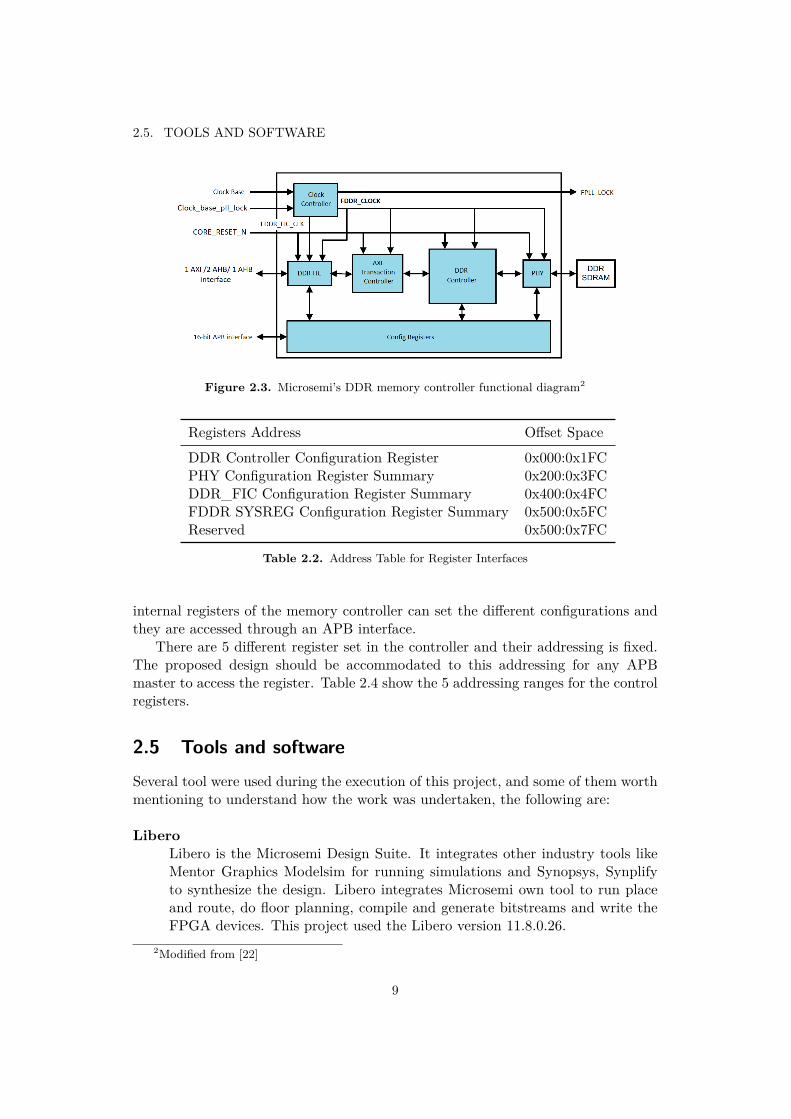
2.4 Microsemi’s DDR Memory controller IPMicrosemi’s memory controller IP is a flexible module designed to interface withDDR2, DDR3, and LPDDR1 memories. It enables single error correction and dou-ble error detection, this makes the IP specially suited for the high reliability re-quirements of the space missions. It supports 8/16/32-bit data bus width modesand a maximum of 8 memory banks. The figure 2.3 depicts the function diagramof the IP.
As showed in the picture the IP includes a clock controller to generate twoclocks, a fabric interconnect clock and the DDR clock. The IP can be interfacedeither 1 or 2 AHB interfaces, or 1 AXI interface for the memory transactions. The
8
2.5. TOOLS AND SOFTWARE
Figure 2.3. Microsemi’s DDR memory controller functional diagram2
Registers Address Offset Space
DDR Controller Configuration Register 0x000:0x1FCPHY Configuration Register Summary 0x200:0x3FCDDR_FIC Configuration Register Summary 0x400:0x4FCFDDR SYSREG Configuration Register Summary 0x500:0x5FCReserved 0x500:0x7FC
Table 2.2. Address Table for Register Interfaces
internal registers of the memory controller can set the different configurations andthey are accessed through an APB interface.
There are 5 different register set in the controller and their addressing is fixed.The proposed design should be accommodated to this addressing for any APBmaster to access the register. Table 2.4 show the 5 addressing ranges for the controlregisters.
2.5 Tools and softwareSeveral tool were used during the execution of this project, and some of them worthmentioning to understand how the work was undertaken, the following are:
LiberoLibero is the Microsemi Design Suite. It integrates other industry tools likeMentor Graphics Modelsim for running simulations and Synopsys, Synplifyto synthesize the design. Libero integrates Microsemi own tool to run placeand route, do floor planning, compile and generate bitstreams and write theFPGA devices. This project used the Libero version 11.8.0.26.
2Modified from [22]
9
CHAPTER 2. LITERATURE REVIEW AND THEORETICAL ELEMENTS
ModelsimModelsim is one of the leaders on digital design simulations, developed byMentor Graphics it is capable to simulate VHDL and Verilog mix model, likethe one used in this project.
SynplifyThis tool is also and industry leader in its area, it can synthesize VHDL andVerilog code for a great variety to target FPGAs. It is capable of doing statictiming analyses to predict the systems speeds and prevent future timing issuesin the circuit.
RTEMSThe Real-Time Executive for Multiprocessor Systems (RTEMS) is a opensource fully featured Real Time Operating System, this is the preferred op-erating system to run on top of ESA space projects[27], and it targets theSPARC V8 microarchitecture of the LEON2-FT. Even though the OS itselfwas not used, their toolchain was in order to create a new bootloader, Withit the code was cross-compiled using sparc-rtems-gcc version 3.2.3 (OAR Cor-poration gcc-3.2.3-20040420/newlib-1.11.0-20030605-4).
2.6 The SpaceWire Standard
The SpaceWire standard purpose is to address the handling of payload data andcontrol information on board a spacecraft. It aims to support equipment compati-bility and reuse at both the component and subsystem levels [7].
It is a bi-directional, full-duplex, high-speed, serial data communication link. Itwas derived from the IEEE-1355 terrestrial standard and is based on Low VoltageDifferential Signaling (LVDS). [19]
2.7 The SPARC V8 architecture
SPARC stands for Scalable Processor ARChitecture, and its version 8 was stan-dardized by IEEE-1754 in 1994. It defines general-purpose integer, floating-point,and special state/status registers and 72 basic instruction operations, all encodedin 32-bit wide instruction formats.[15] The architecture is derive from the reducedinstruction set computer (RISC) lineage, and it is based on the RISC I & II de-signs from the University California Berkeley. The architecture uses the concept of“register windows” in an effort to optimize the code compiling process and easilyimplement pipelining.
The register windows are intended for context switching, at any one instant, aprogram sees 8 global integer registers plus a 24-register window into a larger registerfile. The windowed registers can be described as a cache of procedure arguments,local values, and return addresses.[15]
10

2.8. THE LEON2 FAULT TOLERANT (FT) MICROPROCESSOR
This information and other details about the architecture must be understoodto properly write assembly code and a bootloader as it was necessary during theexecution of this project. To get extra detail the Architecture Manual and theInstruction Set Reference are freely available.
2.8 The LEON2 Fault tolerant (FT) microprocessorThe LEON2-FT is a 32-bit microprocessor based SPARC V8 architecture developedby Gaisler Research for the European Space Agency (ESA) in the year 2000 [8].The design targets space missions of ESA beyond the year 2000, and its main goalwas to create a processor capable to tolerate transient SEU error by design. Withsuch purpose the microprocessor uses techniques as TMR registers, on-chip errordetection and correction (EDAC), parity, pipeline restart and forced cache miss [9].
Through the years the LEON2-FT has being compared with other CPUs. In2005, the Deutsches Zentrum für Luft und Raumfahrt (DLR) compared the perfor-mance of the LEON2-FT with the POWERPC823E and the ARM7TDMI micropro-cessors. All three microprocessors has already been used in spaceborne navigationapplications, and because of that they were benchmarked with a special test casescenario involving orbit propagation for a satellite in Low Earth Orbit (LEO). Atthe end of these experiments it was demonstrated that the ARM processor out-performs the Power PC in CPU time by a factor of two and the LEON processoroutperforms the ARM processor by a factor of 4. [10]
This results is of special interest later on, but it is important to keep in mindthat the ARM7TDMI processor is an implementation of the ARMv4T architecture[3], and the current work will compare the processor with a Cortex-R5 processorswhich uses a more advance ARMv7-R architecture.
2.9 Advanced Microcontroller Bus ArchitectureThe ARM’s Advanced Microcontroller Bus Architecture (AMBA) is one of the mostimportant industry standards for SoC’s design. It allows the interconnection anddesign of different IP by following and open standard. AMBA version 3 includes ahigh speed standard interface known as AXI, but for the ESA the version 2 whichdefines the AMBA high-performance bus (AHB) and AMBA peripheral bus (APB)is still the preferred standard [2].
To implement several Masters the AHB requires a decoder/multiplexer and abus arbiter, this modules are implemented within the LEON2-FT [25].
Within the LEON2-FT architecture the control registers of all modules shouldbe access via APB and the memory transactions should go over the AHB, thenthe proper modifications on the arbiters and decoder should be done to add a newaddressable IP. In the next sections the specifics changes on the AMBA decoderand arbiter would be discussed. All the necessary descriptions of the signals andtransfer types can be found in the AMBA 2 Protocol specification [14]
11
CHAPTER 2. LITERATURE REVIEW AND THEORETICAL ELEMENTS
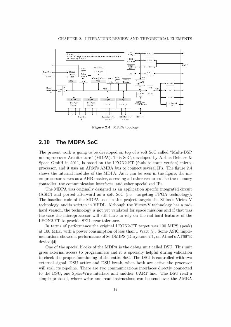
Figure 2.4. MDPA topology
2.10 The MDPA SoCThe present work is going to be developed on top of a soft SoC called “Multi-DSPmicroprocessor Architecture” (MDPA). This SoC, developed by Airbus Defense &Space GmbH in 2011, is based on the LEON2-FT (fault tolerant version) micro-processor, and it uses an ARM’s AMBA bus to connect several IPs. The figure 2.4shows the internal modules of the MDPA. As it can be seen in the figure, the mi-croprocessor serves as a AHB master, accessing all other resources like the memorycontroller, the communication interfaces, and other specialized IPs.
The MDPA was originally designed as an application specific integrated circuit(ASIC) and ported afterward as a soft SoC (i.e. targeting FPGA technology).The baseline code of the MDPA used in this project targets the Xilinx’s Virtex-Vtechnology, and is written in VHDL. Although the Virtex-V technology has a rad-hard version, the technology is not yet validated for space missions and if that wasthe case the microprocessor will still have to rely on the rad-hard features of theLEON2-FT to provide SEU error tolerance.
In terms of performance the original LEON2-FT target was 100 MIPS (peak)at 100 MHz, with a power consumption of less than 1 Watt [9]. Some ASIC imple-mentations showed a performance of 86 DMIPS (Dhrystone 2.1, on Atmel’s AT697Edevice)[4].
One of the special blocks of the MDPA is the debug unit called DSU. This unitgives external access to programmers and it is specially helpful during validationto check the proper functioning of the entire SoC. The DSU is controlled with twoexternal signal, DSU active and DSU break, when both are active the processorwill stall its pipeline. There are two communications interfaces directly connectedto the DSU, one SpaceWire interface and another UART line. The DSU read asimple protocol, where write and read instructions can be send over the AMBA
12

2.11. THE DHRYSTONE BENCHMARK
bus, giving access to all the control registers of the SoC to the user. With thisfeature the memory can be accessed as well, by issuing commands targeting addresswhich are decoded to the memory controller. This feature will be used to validatethe memory interfaces and the proper functioning of the whole system. In theappendix and example program can be read to understand the basic commands ofthe DSU.
2.11 The Dhrystone benchmarkThe Dhrystone “C” test is a computer program developed in 1984 by Reinhold P.Weicker, and it is considered today the standard benchmark for “integer” computingperformance. The original version was written in ADA language, and the C versionwas later written by Rick Richardson. This version is referred as “version 1.1”.
The test includes common constructs found in a broad range of software, itexecutes statements that are balanced in terms of the distribution of statementtypes, data types, and data locality [28]. However, soon after the release of thebenchmark a pitfall became evident, the new developments of the compilers impactthe results of the benchmark, to mitigate this, in 1988 a new “version 2.1” wasreleased [29].
The Dhrystone test uses a different measuring unit than rather simple “millionof instructions per second”, the so called “Dhrystone MIPS” or DMIPS. Since aRISC machine may require more instructions than its CISC counterpart to executethe same task, the benchmark counts the number of program iterations, a DMIPSis defined as the number of loops divided by the score of a reference machine, inthis case the VAX11/780, with a value of 1757. This value is arbitrary, and whencomparing two CPUs any can be set as reference, but when referring to DMIPS theoriginal reference value should be used.
The test is being criticized since it is susceptible to compiler optimizations[31], this will be clearly evidenced later on this document with the Cortex-R5performance specifications. To overcome this issues the Embedded Microproces-sors Benchmark Consortium (EEMBC) has release CoreMark in 2009, but olderCPUs have no benchmarking data making difficult its usage with processors likethe LEON2-FT. Another pitfall worth mentioning is the difficulties found whencomparing CPUs with Harvard vs Von Neumann architectures, since the small sizeof the test code fits in the instruction cache, this prevents the testing of the instruc-tion fetch when having a separate instruction cache.
13

Part II
Design proposal and implementation
15

Chapter 3
Design proposal and implementation
This chapter approaches the first part of the work done during the thesis project.It goes over the rational of the design decisions and afterwards presents a newarchitecture for the SoC, taking off from the baseline of the MDPA. Finally thesecond part of the chapter covers the details in the implementation process followedafter the proposal, and the difficulties found.
3.1 Design proposal
Two design objectives drive the proposal, first to enhance the memory hierarchy ofthe Airbus’ MDPA SoC by adding support for the DDR3 memory technology, andsecond to explore the usage of the Microsemi’s radiation hardened FPGA technol-ogy (RTG4). Enhance the memory hierarchy means to increase its capacity andbandwidth and exploration of the RTG4 technology implies to look for the bestusage of the FPGA resources. With this in mind, several parts of the design shouldbe planned and for that purpose the work was divided into two stages.
The first stage is focused on the existing structures, which are FPGA technologydependent; the logic should be ported from the Virtex-V to the RTG4 technology.This process includes the porting of I/O pads and buffers, memories (inferred andnon-inferred), and finally the clock and reset unit. During this process, the changesare not radical, but to do a good use of resources special care must be taken.Inferring memories might not be optimal and the timing characteristics of the RTG4macros might impact the results if not considered carefully.
The second stage is the addition of the memory controller itself, by using theIP from Microsemi. The code will be generated with the Microsemi’s GUI, andthen instantiated properly in the SoC’s code. It is here where most of the work iscentered and the one that requires time on debugging and study, if wrong decisionson the proposal are done the rework might cost a lot.
17

CHAPTER 3. DESIGN PROPOSAL AND IMPLEMENTATION
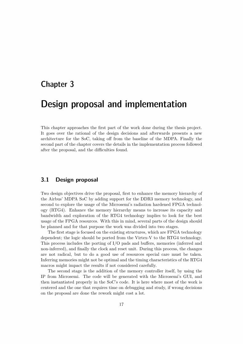
3.1.1 Design stage oneThe clock and reset controller is highly dependent on which FPGA technology isbeing used, and due to that the design has to be implemented through the Mi-crosemi’s macro library. The macro library lets designers use a clock conditioningcircuit (CCC), which is very flexible and allows several configurations. Withinthe RT4G150 device there are 8 CCC components, and each one has a dedicatedradiation-hardened triple redundant PLL for clock synchronization [21]. Microsemiprovides through its software Libero, a GUI to easily add and configure CCCs.
The requirement from design is to generate two clock domains to be globallydistributed, this means clock signals that drive the clocking global networks of theFPGA, with respectives frequencies of 40MHz and 100MHz The RTG4 technologyprovides up to 24 global clock buffers, this means that 2 clock domains representsa fairly simple design from the clocking perpective.
The CCCs allow 3 different inputs sources as clock reference for the PLL.
• A 50Mhz oscillator is internally provided,
• An external clocks
• An internal fabric input
Jitter and precision will be disregarded as design factors, since this is fixed bythe FPGA fabric. Two clock domains are required, the CPU clock is the main clockof the system, feeding most of the design. A second clock domain required is a100 MHz clock for the SpaceWire, even though this will only be used optionallyfor the debug unit as a secondary interface. Additionally this clock is generatedfrom the interface itself, and should only be considered when writing the timingconstraints during synthesis, it is not part going to be included in clock and resetunit. For future work, the CCC macro includes special dedicated circuitry whichcan be used to substitute some of the code included in the SpaceWire IP providedwith the MDPA, although this will not be included in the proposal. The figure 3.1shows the GUI to generate CCC macro code, here 4 clock are connected, but thefinal implementation includes just the main system clock.
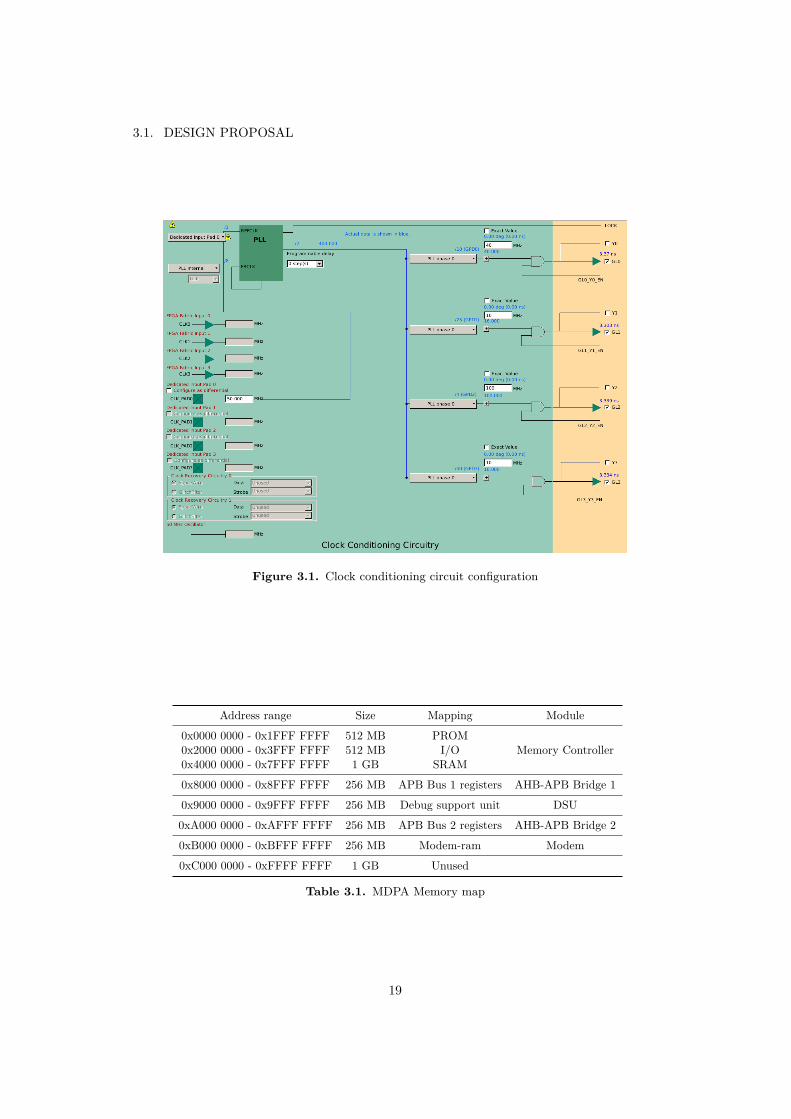
3.1.2 Design stage twoIn the stage two changes over the architecture of the SoC are to be defined. Asany design there exist constraints, and those will impact and model the proposal.The first constraint to consider is the target hardware. In this case this is theMicrosemi’s Development Kit, which features a RT4G150 device, covered in sec-tion 2.2. It includes 8 256MB Micron DDR3 memory chips (MT41K256M8DA-125IT:K), divided in two DDR ports. This means that there are 2 GB of memoryavailable, but new memory should fit in the MDPA memory map. The originalmemory map of the MDPA implementation allocates the memory ranges showed inthe table 3.1.2.
18
3.1. DESIGN PROPOSAL
Figure 3.1. Clock conditioning circuit configuration
Address range Size Mapping Module
0x0000 0000 - 0x1FFF FFFF 512 MB PROM0x2000 0000 - 0x3FFF FFFF 512 MB I/O Memory Controller0x4000 0000 - 0x7FFF FFFF 1 GB SRAM
0x8000 0000 - 0x8FFF FFFF 256 MB APB Bus 1 registers AHB-APB Bridge 1
0x9000 0000 - 0x9FFF FFFF 256 MB Debug support unit DSU
0xA000 0000 - 0xAFFF FFFF 256 MB APB Bus 2 registers AHB-APB Bridge 2
0xB000 0000 - 0xBFFF FFFF 256 MB Modem-ram Modem
0xC000 0000 - 0xFFFF FFFF 1 GB Unused
Table 3.1. MDPA Memory map
19
CHAPTER 3. DESIGN PROPOSAL AND IMPLEMENTATION
The new DDR memory should be allocated within this area, and also it isdesirable to keep SRAM memory range, for backward compatibility and later usefor comparing the SRAM with the DDR memory. Then there is just enough space toallocate 1GB of memory within the unused memory space. Finally, the last changein the memory space will be in the Modem memory area. The area along with themodule itself is going to be removed, leaving 256 MB of unused memory space.
The main goal is to use the IP Module provided by Microsemi, (refer to sub-section 2.4, for detail information about the IP), for that 7 KB of memory shouldbe allocated for the control registers of the IP. Any of the AHB-APB Bridges haveenough memory space to be connected to the IP Then the proposal is to allocate theDDR memory in the range that goes from 0xB000_0000 to 0xEFFF_FFFF, andthe control registers will be addressed in the range that goes from 0xA000_1000 to0xA000_1FFF.
As mentioned before the SoC is build using AHB and APB AMBA fabrics,and the memory controller IP can be configured to use one or two AHB interfaces.By using two AHB slaves the memory controller can provide twice the bandwidth,but this is only useful when using two AHB networks. The MDPA SoC uses onlyone network. The implementation of the LEON2-FT cache controller has only oneread/write port, if another port can be implemented in the cache controller, speciallyconsidering that the SPARC V8 architecture has separate instruction and datacaches, a second AHB fabric can be used. But this option implies the modificationof the cache controller logic, this is out of the scope of this work, and then thedesign proposed should use only one AHB slave port on the memory controller.
3.1.3 Theoretical limits
The design has limits and these can be estimated and later on confirmed after theimplementation. In this case the relevant values are two, first the performance of theCPU, since the migration to a new FPGA technology should imply no degradationon the performance of the system, and second with uttermost importance, theperformance of the internal RAM and the DDR memory (i.e. memory bandwidthand latency).
The performance of the CPU in this case is the speed in MIPS that the processorcan reach. Theoretically the LEON2-FT pipeline should be able to achieve a peakspeed of 1 instruction per cycle, this means 40 MIPS at 40 MHz (i.e. 1MIPS/MHz).But not all instructions are executed in 1 clock cycle so the peak performanceis hardly reached and maintained in normal execution time. The goal is then todemonstrate the after the implementation that a peak performance of 1MIPS/MHzis still reachable.
Referring to the DDR memory controller there are several considerations. Theperformance of the memory hierarchy depends on several components. The band-width of the DDR is fixed for the memory technology depending on the DDR clockfrequency. For this design a frequency of 320 MHz is used, this provides a bandwidthof 20460 Mpbs following the equation 3.1.3.
20

3.1. DESIGN PROPOSAL
DDRbw = bus_freq ∗ 2 ∗ bus_width
Figure 3.2. DDR3 max bandwidth
Figure 3.3. AHB-Lite transaction cycles3
In the AHB bus, the max bandwidth is achieved when generating back to backtransactions. Given the fact that the LEON2-FT has only one write/read cacheport, which generate 32 bits wide transactions, and then no burst transactions aregenerated over the AHB bus. This means that every single transactions requirestwo cycles at the bus frequency, considering that the transactions require an addresscycle and an data cycle, as depicted in the figure 3.3. Then 2 clock cycles are requiredto transmit 32 bits.
Finally, if arbitration is disregarded, and the initialization is already done, thismeans that the max performance of the AHB bus is 32 bits times 40MHz dividedby 2 (cycles per transaction), this is 640 Mbps (Mega bits per second).
The next element is how much peak bandwidth can the CPU theoretically con-sume. As mentioned before the max performance of the LEON2-FT is 1MIPS/MHz,and assuming that a long run of instructions is composed by only continuous mem-ory non-blocking transactions, the core will generate at peak condition 40 MT/s at
3Modified from [14]
21
CHAPTER 3. DESIGN PROPOSAL AND IMPLEMENTATION
Element bandwidth (Mbps)
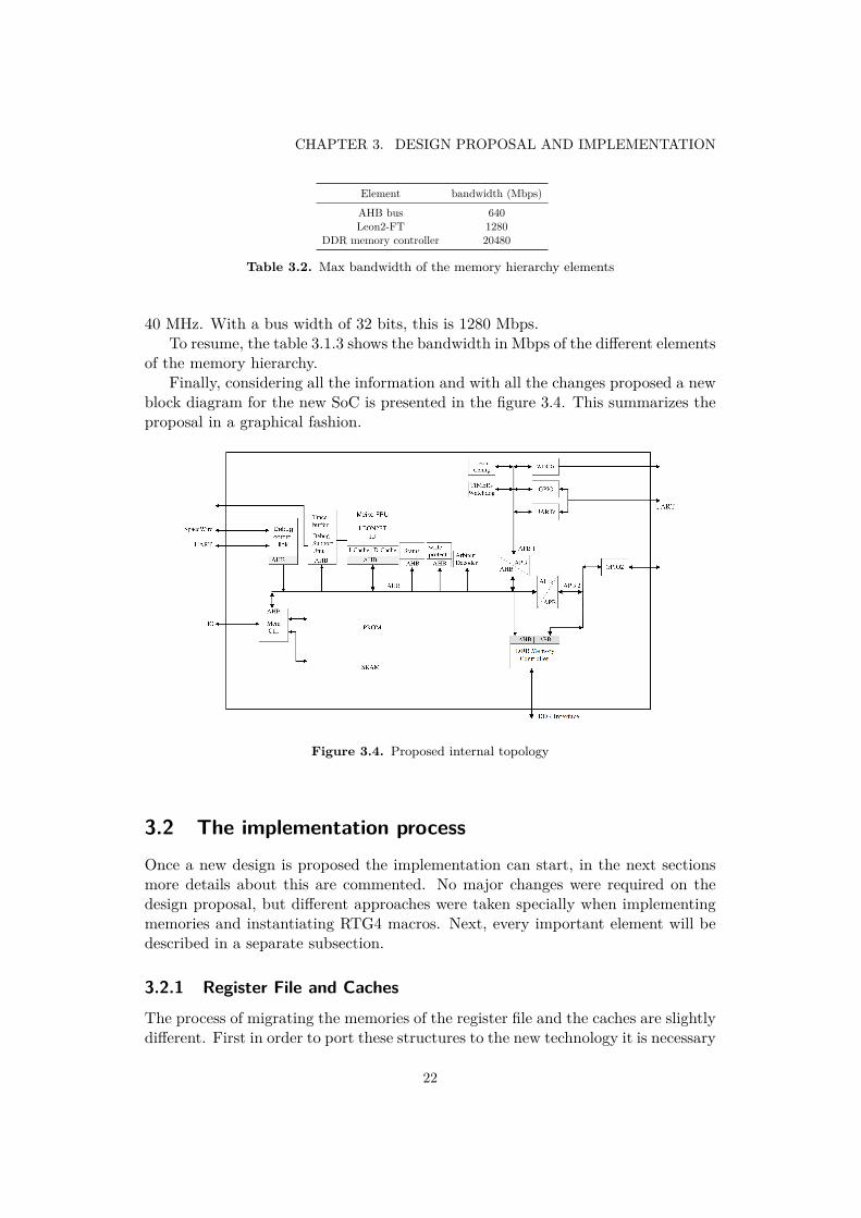
AHB bus 640Leon2-FT 1280
DDR memory controller 20480
Table 3.2. Max bandwidth of the memory hierarchy elements
40 MHz. With a bus width of 32 bits, this is 1280 Mbps.To resume, the table 3.1.3 shows the bandwidth in Mbps of the different elements
of the memory hierarchy.Finally, considering all the information and with all the changes proposed a new
block diagram for the new SoC is presented in the figure 3.4. This summarizes theproposal in a graphical fashion.
Figure 3.4. Proposed internal topology
3.2 The implementation processOnce a new design is proposed the implementation can start, in the next sectionsmore details about this are commented. No major changes were required on thedesign proposal, but different approaches were taken specially when implementingmemories and instantiating RTG4 macros. Next, every important element will bedescribed in a separate subsection.
3.2.1 Register File and Caches
The process of migrating the memories of the register file and the caches are slightlydifferent. First in order to port these structures to the new technology it is necessary
22

3.2. THE IMPLEMENTATION PROCESS
A_ADDR/B_ADDRDepth x Width Used Bits Unused Bits (to be grounded)
512 x 36 (Two-port) [10:2] [1:0]
Table 3.3. Address bus configuration for Two-port mode
to identify the structure of the memories.For the register file the memory requires synchronous, single write port, dual
read port. With 8 bits wide address bus and 36 bits data bus (the last 4 bits arefor EDAC). While for the caches the memory uses that very same configuration forthe data cache (instantiated several times to make a full cache line), and almost thesame, but with the exception of a single read port instead of a double port, for theinstruction cache.
There are three options to implement the register file. The first option is to inferthe memory and beside that, the is another two options. The first option is to usethe Large SRAM memories. There is only one internal memory configuration thatallows to have 36 bits wide data bus, this configuration is called two-port 512x36,table 3.2.1 shows the configuration from the Microsemi’s macros specification.
Then, to implement the memory 4 memory blocks (RAM1K18_RT) are re-quired. The other option is to use small memory blocks (µSRAM) but given theamount of memory necessary, this will consume to many resources and would bewasteful.
The third option is to infer the memories with a block of VHDL code. Afterdoing this the best results consumes 6 LSRAM blocks for the register file instead of4. A cascade configuration generated by the inferencing software uses the macrosin a 128x12 fashion instead of the 512x36 alternative as follows:
• Port A configuration : 128x12• Port B configuration : 128x12• Port C configuration : 128x12• Number of blocks depth wise: 2• Number of blocks width wise: 3
This wastes more memory and the best implementation option is the 4x512x36configuration. But later on during synthesis timing issues were found. This becausethe register file is critical for the CPU to work properly and at maximum speed.After synthesis using the 512x36 configuration, the critical path of the design wasfound between the register file and the integer unit (IU). To fix this problems theregister file was implemented using flip-flips instead of memory macros. This bumpthe slack time of the paths involving the register file, at expenses of logic elementson the FPGA.
To implement the caches a big amount of memory is required, the cache config-uration is stated in the table 3.2.1. In this case the aforementioned 512x36 config-
23

CHAPTER 3. DESIGN PROPOSAL AND IMPLEMENTATION
Instruction cache 32 KbyteAssociativity 4 wayCache line size 32 ByteReplacement policy Last recently used
Data cache 16 KbyteAssociativity 2 wayCache line size 16 ByteReplacement policy Last recently used
Table 3.4. Cache configuration
Speed Grade Data Rate (MT/s) Target tRCD-tRP-CL tRCD (ns) tRP (ns) CL (ns)
-125 1600 11-11-11 13.75 13.75 13.75
Table 3.5. Memory timing parameters
uration was used, the whole cache memory was implemented with several instancesand no timing of functional issues were found.
The next block to be implemented is the new DDR memory controller.
3.2.2 DDR Memory controller
The Microsemi’s configurator graphical user interface (GUI) was used to generatethe basic VHDL interface of the IP. Then with the code interface of the Microsemi’sblackbox macro all code was written to wrap and connect the interfaces. Thisincludes the AHB and APB interface. As prosed the APB was connected to thebridge 2, modifications were made to the bridge to it internally. The addressingwas extended 4 bits, this means that the bridge had to be modified to consideratethose extra bits in the arbitrating process. Later the DDR interface was connectedall the way up to the top level design to make sure the interface reaches the SoC’sIO pins.
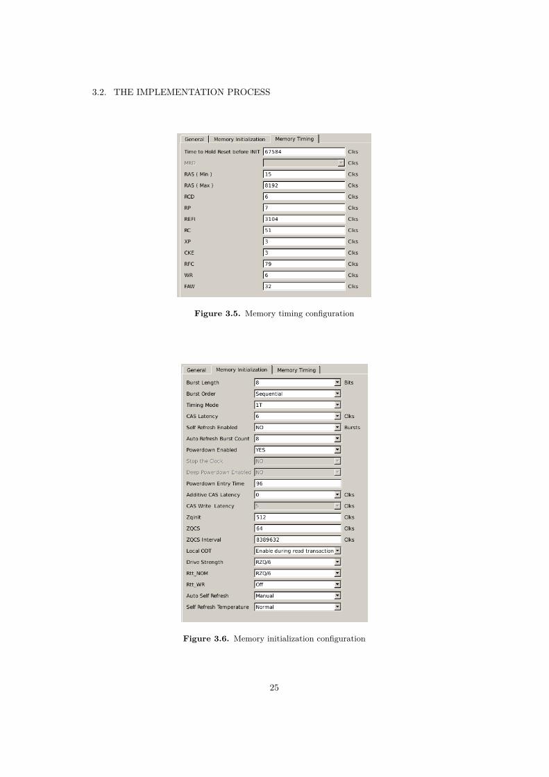
The configuration of the memory controller depends directly on the DDR mem-ory chip being used. The timing values for the memory are required to write downthe bootloader configuration sequence. These parameters are showed in figure 3.5and the required the most significant information from the device specification isgiven in the table 3.2.2, (although not the only one necessary).
The values for timing used in the proposed configuration are specifically set torun at 320 MHz. These are recommended by Microsemi, but they can be modifiedas required when a different target is used or if another speed is required.
Apart from the timing configuration, the initialization process of the memoryhas another set of parameters that must be properly configured for the memorycontroller to communicate with the memory chips.
The figure 3.6 shows the initialization configuration. Among the most importantsettings here are the column-address strobe (CAS) latency and the timing mode.The CAS latency is selected according to the DDR memory, in this case 6 clockunits of the target memory.
24
3.2. THE IMPLEMENTATION PROCESS
Figure 3.5. Memory timing configuration
Figure 3.6. Memory initialization configuration
25
CHAPTER 3. DESIGN PROPOSAL AND IMPLEMENTATION
The timing mode is 1T, and as stated in the IP documentation. “In 1T, theDDR controller can issue a new command on every clock cycle. In 2T timing, theDDR controller holds the address and command bus valid for two clock cycles. Thisreduces the efficiency of the bus to one command per two clocks, but it doubles theamount of setup and hold time.”[22]
With all this the IP was wrapped in the SoC code and with all the information,a new bootloader should be written.
3.2.3 The bootloaderThe bootloader is the program that starts up the SoC. Because all the changes inthe hardware a new bootloader is required. The program is naturally written in theSPARC assembly language, and it is loaded into the ROM. The basic purpose is toinitialize the machine, and the minimum set of task included are:
• Clean the cache by flushing it.
• Set the memory configuration.
• Clean all the output, local and global general purpose registers of the SPARCmicroarchitecture for the available windows.
• Configure the floating point unit.
• clean all the floating point general purpose registers.
• Enable the traps.
• Set the stack and frame pointers.
• Jump to the RAM memory area for main program (OS most probably) exe-cution.
All this actions are executed linearly and basically no flow control loops arerequired, (with the exception of waiting loops). The provided implementation ofthe LEON2-FT comes with a bootloader in binary form. In order to generate a newbootloader, the RTEMS’ objdump tool was used to disassemble the content. Thisprocess has been done before in the past, and a set of headers is later used to mapthe MDPA control registers. With the code in assembly code ready the requiredmodifications where performed, this includes:
• Changing the jump to RAM memory area to the new DDR memory area.
• Cleaning unnecessary register due to modules removal.
• Change the memory configuration to match the internal RAM configuration.
• Add the DDR memory controller set up.
26

3.2. THE IMPLEMENTATION PROCESS
This final point is crucial for the proper working of the DDR memory controller.The memory controller IP is very flexible is supports a big variety of configurations.To compile the new bootloader a makefile was written to ease the process of callingthe RTEMS-GCC compiler. The coding of the makefile is of special usage to gen-erate the binary version of bootloader, this is due to the fact that the binary mustbe converted to a proprietary Microsemi format. To translate the binary file a shellscript was coded, this script will parse the binary output of GCC and return thecode ready to be loaded in the micro programmable read only memory (µPROM)both for simulation and synthesis. The code snippet 3.1 show the format, which isa text file with rows of thirty six “1” or “0” characters. Every row is preceded bythe line number in hexadecimal base starting with an “at” sign (@).
Code 3.1. µPROM memory content excerpt
@0000010000001110110000010000000000000@1000000001111001000000000000000000000@2000000000011000001010000001000000000
3.2.4 IO constraintsThe process of writing the IO constraints requires the gathering of the correctinformation from the specifications of the RT4G150 device and the development kitboard. Originally the intended interfaces were only the following:
• UART-DSU
• SpaceWire-DSU (removed)
• SpaceWire (removed)
• GPIOs
• LEDs
• DSU control lines
But due the reset limitations of the technology the SpaceWire interfaces had tobe removed. The mapping of the RT4G150 device in the development board canbe done also with some help from the Libero GUI, as depicted in the figure 3.7.
27

CHAPTER 3. DESIGN PROPOSAL AND IMPLEMENTATION
Figure 3.7. Libero GUI for IO constraints
28

Part III
Verification and validation results
29

Chapter 4
Verification process
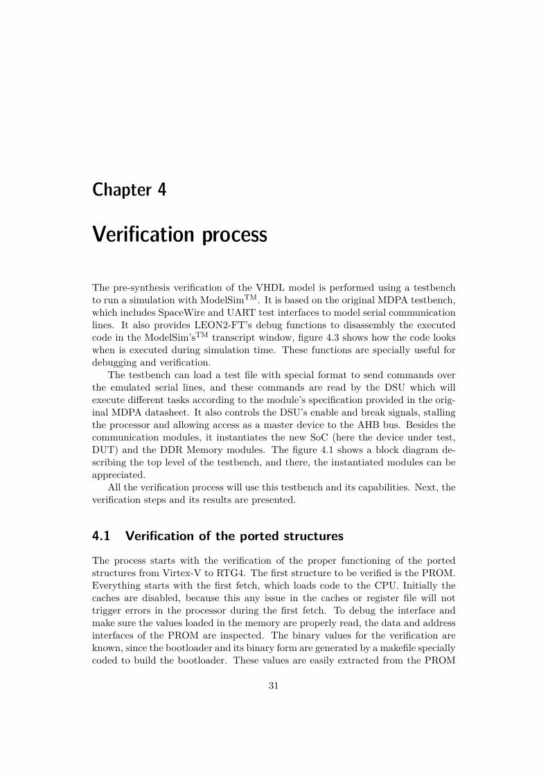
The pre-synthesis verification of the VHDL model is performed using a testbenchto run a simulation with ModelSimTM. It is based on the original MDPA testbench,which includes SpaceWire and UART test interfaces to model serial communicationlines. It also provides LEON2-FT’s debug functions to disassembly the executedcode in the ModelSim’sTM transcript window, figure 4.3 shows how the code lookswhen is executed during simulation time. These functions are specially useful fordebugging and verification.
The testbench can load a test file with special format to send commands overthe emulated serial lines, and these commands are read by the DSU which willexecute different tasks according to the module’s specification provided in the orig-inal MDPA datasheet. It also controls the DSU’s enable and break signals, stallingthe processor and allowing access as a master device to the AHB bus. Besides thecommunication modules, it instantiates the new SoC (here the device under test,DUT) and the DDR Memory modules. The figure 4.1 shows a block diagram de-scribing the top level of the testbench, and there, the instantiated modules can beappreciated.
All the verification process will use this testbench and its capabilities. Next, theverification steps and its results are presented.
4.1 Verification of the ported structures
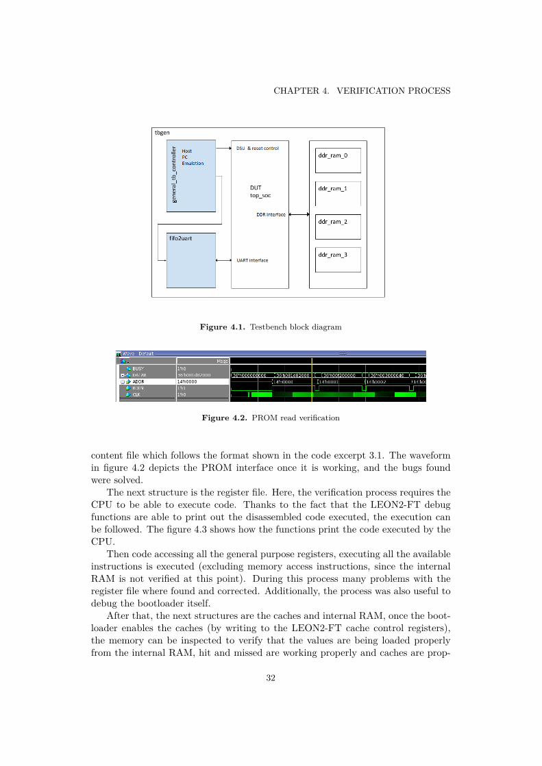
The process starts with the verification of the proper functioning of the portedstructures from Virtex-V to RTG4. The first structure to be verified is the PROM.Everything starts with the first fetch, which loads code to the CPU. Initially thecaches are disabled, because this any issue in the caches or register file will nottrigger errors in the processor during the first fetch. To debug the interface andmake sure the values loaded in the memory are properly read, the data and addressinterfaces of the PROM are inspected. The binary values for the verification areknown, since the bootloader and its binary form are generated by a makefile speciallycoded to build the bootloader. These values are easily extracted from the PROM
31
CHAPTER 4. VERIFICATION PROCESS
Figure 4.1. Testbench block diagram
Figure 4.2. PROM read verification
content file which follows the format shown in the code excerpt 3.1. The waveformin figure 4.2 depicts the PROM interface once it is working, and the bugs foundwere solved.
The next structure is the register file. Here, the verification process requires theCPU to be able to execute code. Thanks to the fact that the LEON2-FT debugfunctions are able to print out the disassembled code executed, the execution canbe followed. The figure 4.3 shows how the functions print the code executed by theCPU.
Then code accessing all the general purpose registers, executing all the availableinstructions is executed (excluding memory access instructions, since the internalRAM is not verified at this point). During this process many problems with theregister file where found and corrected. Additionally, the process was also useful todebug the bootloader itself.
After that, the next structures are the caches and internal RAM, once the boot-loader enables the caches (by writing to the LEON2-FT cache control registers),the memory can be inspected to verify that the values are being loaded properlyfrom the internal RAM, hit and missed are working properly and caches are prop-
32

4.1. VERIFICATION OF THE PORTED STRUCTURES
Figure 4.3. Disassembled code executed by the CPU
erly instantiated. Loading values directly into the RAM is possible now, and thosevalues can be checked and confirmed in simulation time.
Here an actual difficulty was found. In order to generate the code of the internalRAM several identical modules where instantiated. Because of this, loading differentcontent files requires rework. Non continuous data can be loaded without problemsbut it is not easy to load code since consecutive blocks of RAM will share identicalcode, making the code almost unusable. This is not a problem for verificationspurposes, but it is for future purpose like loading software for benchmarking, ormore complex programs . The solution to this is to load RAM code the via DSU,this will be covered later on the document, but the general idea is to stall the CPUbefore the final jump of the bootloader, load the RAM with a program (or an entireOS), and then resume execution.
Once the verification of the Internal RAM and caches is over, the final step in theverification process is the DDR memory controller. Here the process becomes foriterative, debugging and recoding is constant and most of the time of the verificationprocess was consumed. The first step is to make sure that the APB and AHBinterfaces of the memory controller are working, and that the changes proposed forthe addressing and decoding are properly implemented.
Finally the memory controller requires an specific booting sequence, this se-quence is part of the the bootloader. The complete configuration can be found inthe appendix.
Then the verification of the write and read sequences in the DDR is performed,in this case the data transmitted can be verified in the simulation by checking theoutput signals Figure 4.4 shows the write sequence of the DDR interface.
This process requires also debugging of the testbench, specially because theDDR memory model is implemented in Verilog, and the interfacing with the VHDLtestbench might produce timing problems. Modeling a DDR memory device is
33

CHAPTER 4. VERIFICATION PROCESS
Figure 4.4. DDR write sequence
complex, but the manufacturer provides the model and all the parameters requiredto properly model the specific device used in the development kit board.
Finally a DSU test was created to verify that the debug interface is able toaccess both memories, this test is rather simple, but is fundamental to ensure thatthe system can be validated on the target hardware.
Once the verification process is over, the performance on simulation of the im-plemented DDR memory can be measured, the next sections the results of thebandwidth and latency of both memories are presented.
4.2 Bandwidth and latency determination on simulationTo determine the performance of both memories implemented in the SoC a set oftests were written in SPARC assembly and appended inside the bootloader. Thismeans that these tests are executed from internal ROM of the SoC, without usingthe DSU interface.
Three simple tests were coded to measure the bandwidth consumed by theLEON2-FT, and whit them determine if any of the memories is generating back-pressure in the memory hierarchy. All the tests run with the following configuration:cacheable memory on and write through cache policy, the test are the following:
• 100 loops of 10 writes
• 100 loops of 10 reads
• 200 loops of 10 read after write sequences
For every test there is one instruction overhead per memory access due to thenecessity of increasing the address variable used as pointer and 3 instructions over-head per cycle required for the jumps and flow control. Because of this the maxbandwidth is not reached.
The tables 4.2, 4.2, and 4.2 resume the results of tests. The code used for one ofthe tests is included in the appendix. During verification the times where measuredwith the waveforms but the test also includes code to use the timers to measure thetime, expecting to get the same results in validation.
34

4.2. BANDWIDTH AND LATENCY DETERMINATION ON SIMULATION
Internal RAM DDR
Sequential writes 1000 1000Total number of instructions 2300 2300
MIPS 14,81 21,18Simulation time (ns) 155250 109600
Mega transactions per second 6,44 9,21
Consumed bandwidth (Mbps) 206,12 294,66
Table 4.1. Bandwidth consumption over sequential writes
Internal RAM DDR
Sequential writes 1000 1000Total number of instructions 2300 2300
MIPS 12,31 10,43Simulation time (ns) 186775 220525
Mega transactions per second 5,35 4,53
Consumed bandwidth (Mbps) 171,33 145,11
Table 4.2. Bandwidth consumption over sequential reads
Internal RAM DDR
Sequential Read after write 2000 2000Total number of instructions 3300 3300
MIPS 16,35 19,13Simulation time (ns) 201850 172525
Mega transactions per second 9,91 11,6
Consumed bandwidth (Mpbs) 317,07 370,96
Table 4.3. Bandwidth consumption over sequential reads after writes
35

CHAPTER 4. VERIFICATION PROCESS
Figure 4.5. Internal RAM read latency measurements
The results show that under a this “normal” conditions it is hard to achieve thepeak bandwidth of the slower element to memory hierarchy, i.e. the AMBA bus onsingle burst-32-bits configuration. Although the LEON2-FT core is far from gener-ating its peak performance (40 MIPS at 40MHz), the memory access instructionshave a penalty in the pipeline that will never allow this condition to happen. Theintention of the test is to measure the bandwidth under the fix set of conditions,to serve as a verification test and not as benchmarking or measuring maximumperformance. A more proper test should be run in validation, using a benchmarkslike Dhrystone or Hartstone which are studied and properly designed. The resultspresented before, are good enough to verify that the behavior of the memory hi-erarchy is within the expected and properly functioning, while demonstrating thatthe performance of the SoC if far from consuming all the bandwidth that can beget from the DDR3 memory.
The next test was to measure latency and the process goes as follows. Singlewrites or reads are performed and then the time between issuing and completingthe transaction is measured with the wave forms. The figure 4.5 shows the mea-surements of the latency for the internal RAM memory when reading.
This latency considers the total time of the transactions, this is the latencyof the AHB bus, the respective memory controller, either internal RAM or DDR,and the device latency. It is important to recall that when the device latency ofthe DDR memory depends on the selected chip, the internal RAM is fixed for theRTG4 technology. The process of running simulations was done for both memories,and summarized in the table 4.2.
As expected read transactions are slower than writes since the transactions mustgo back and forth, passing over the memory controller and AHB bus twice.
36
4.3. SYNTHESIS
Internal RAM DDR
Read (ns) 875 1025Write (ns) 600 406,46
Table 4.4. Memory access latencies
4.3 Synthesis
The process of synthesis was executed in parallel with the model verification. Itwas done by the Synplify’s synthesis tool, and the first step was to create the clockconstraints. Defining the clock is the most important constraint and is necessary forthe tool to identify the clock signals (there is no differentiation from normal signalsin VHDL), to determine the clock domains and run the static timing analysis.
Defining the system clock, and the input clock (when using an external oscillator,which is this case) is absolutely necessary. The code excerpt 4.1 shows the definitionin Synopsys design constraint (SDC) format. This format is a de-facto industrystandard adopted by different tool and the constraints can be reused easily.
Code 4.1. Clock definitions
define_clock {n:i_reset_clock_controller.CLK0} -name {CLK0} -freq40 -clockgroup main_clk_grp
define_clock {p:clkin} -name {CLKIN} -freq 50 -clockgroup clkin
Other clocks had to be declared like the CAN bus, and the SpaceWire clockinterface, if used but they were not strictly necessary in this case. The unnecessaryclock signals where removed later on the design.
Once this process was complete the synthesizer compiled an area and timingsummaries for the designer to confirm if the model fits the requirements. The en-coding of the finite state machines (FSM) has an special impact on both elements,area an timing. The following encoding schemes were tested: one hot, gray, sequen-tial, and the Synplify’s proprietary FSM optimizer. The results in area and timingare shown in the figures 4.6 and 4.7.
As it can be seen the best option in the Synplify’s proprietary optimizer andthen it was the selected option.
Resources Usage
Once the synthesis process was completed the amount of resources used was reviewedto confirm that the model fits, and it can be hierarchically explored to confirm nounit is missing, the final results are depicted in the table 4.3.
Clearly the resource that is being consumed the most is the LSRAM memoryblock, this is due to the implementation of the internal RAM. It is important to
37

CHAPTER 4. VERIFICATION PROCESS
Figure 4.6. Impact on LUT resources of the encoding schemes
Figure 4.7. Impact on the slack of the encoding schemes
remember that only one of the memory is strictly required, either internal RAM orDDR memory.
Timing analysis
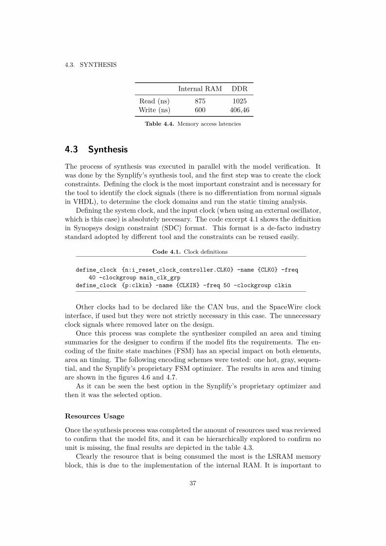
With the synthesis process completed, Synplify generates a static timing analysiswhich gives the designer the possibility to determine the max speed at which thedesign can run. The maximum is speed is limited by the critical path, which isdepicted in the figure 4.8, for the implemented model. The detailed information ofthe critical path is included in the appendix.
Here is noticeable that the critical path is composed by only 4 combinationalcomponents. The number of combinational components is highly associated to
38
4.3. SYNTHESIS
Figure 4.8. Design’s critical path
39

CHAPTER 4. VERIFICATION PROCESS
Type Used Total Percentage
4LUT 27632 151824 18.20DFF 12150 151824 8.00
I/O Register 0 2151 0.00User I/O 86 717 11.99
Single-ended I/O 76 717 10.60Differential I/O Pairs 5 358 1.40
RAM64x18 7 210 3.33RAM1K18 164 209 78.47MACC 1 462 0.22
H-Chip Globals 8 48 16.67CCC 1 8 12.50
RCOSC_50MHZ 0 1 0.00SERDESIF Blocks 0 6 0.00
FDDR 1 2 50.00µPROM 1 1 100.00GRESET 1 1 100.00RGRESET 8 206 3.88
Table 4.5. Resource usage
the ability of the synthesizer to optimize the design, but also on the design itself.Also the technology plays an important role, RTG4 technology has 4 input LUT,while other technologies have up to 6 inputs LUTs, like the Virtex-V technology.Additionally, the ability of the synthesize software to accommodate the logic playsa fundamental roll. Here, the idea is to compare the technology with the sameLEON2-FT core and then giving both implementations a fare opportunity whencomparing the results.
During the process of implementation the critical path was not fast enough atthe beginning. To correct this, there exists several alternatives.
The first options is to change something in the logic. But, since the LEON2-FTis a validated design, it is desirable to make minimum changes to its architecture,this means there is little space to change the logic
The next option is to analyze the path to find if the path can be considered amulti cycle path and then create a timing constraint to tell the synthesize tool totake that into consideration when running and executing the static timing analysis.But here this was not the case
The last option is to change the memory configuration. The RTG4 macros canrun in 4 different configurations (depicted in table 4.3), each configuration as adifferent read access time that impacts the timing. When using the output of thememory in bypass fashion the memories are slower than when using pipelined mem-ories. A VHDL directive was added to change the configuration and dramatically
40

4.3. SYNTHESIS
Parameter Configuration value (ns)
OUTPUT=PIPELINE 2.718Read Access Time (tCLK2Q) ECC=OFF,OUTPUT=BYPASS 7.021
ECC=BYPASS,OUTPUT=BYPASS 7.266ECC=PIPELINE,OUTPUT=BYPASS 5.135
Table 4.6. Internal memory read access time
Figure 4.9. Clock relationships
Required Frequency Estimated Frequency Slack time
System clock 40 MHz 40.8 MHz 0.344
Table 4.7. Internal memory read access time
impact the slack time of the critical path, solving many issues and having no impacton the functionally of the design.
Finally an static timing analysis was executed and the frequency requirementswere meet. The clock relationships between different clock domains, and all theslack times are showed in the figure 4.9. The final results are summarized in thetable 4.3.
Now, when comparing the results obtained of the estimated frequency of thedesign, against the original MDPA results when implemented on Virtex V, it isnoticeable that there was an impact on the speed. The table 4.3 contrasts bothresults.
But the RTG4 provides TMR rad-hard registers saving resources and improvingthe reliability of the design. The table 4.3 shows the resource utilization of LUTsand registers in comparison between both technologies. The whole SoC cannot
Technology Estimated Frequency
Virtex V 59.1 MHzRTG4 40.8 MHz
Table 4.8. Frequency results comparison
41

CHAPTER 4. VERIFICATION PROCESS
Technology LUTs Registers Total available Used percentage
Virtex V 7834 2071 131072 %7,56RTG4 12729 2297 120108 %12,51
Table 4.9. Resources usage against Virtex V
be directly compared since not all the same modules exists in both designs, thenonly the LEO2FT core can be directly compared. Although the RTG4 technologyrequires more registers to implement the core, in the RTG4 design uses extra flipflops since the cache tags are implemented with flip flops instead of macro memoriesto help with the timing of the critical path. Those resources (536 registers), areconsumed in the Virtex V in form of memory elements.
Place and route
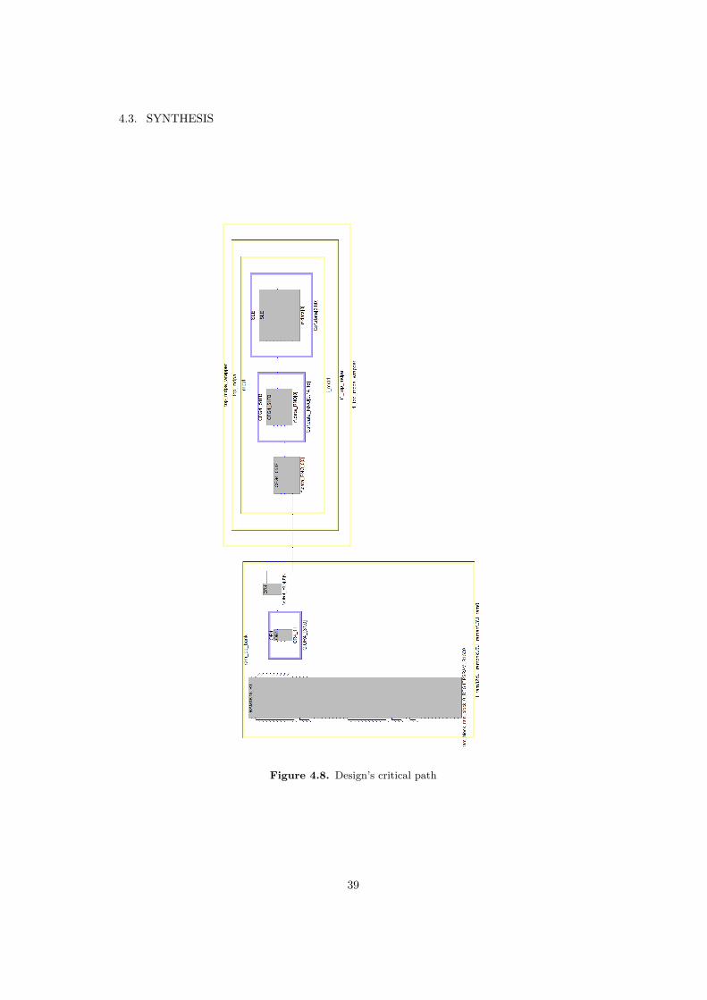
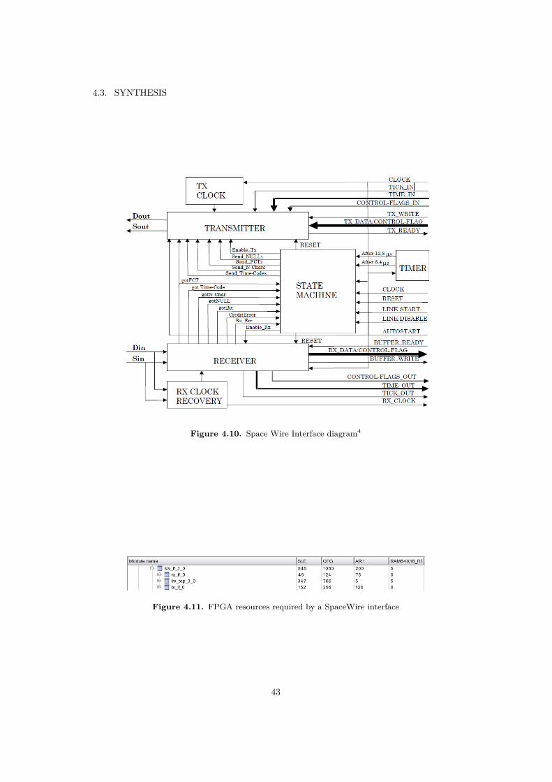
When running place and route with the first running model, the Libero place androute tool was not able to find a feasible placing. The reason for this was the amountof asynchronous resets required by the SpaceWire interface. As shown in the figure4.10, every space wire link, has 3 independent reset signals, and every interfacecan be implemented with very few logic elements. As shown in the figure 4.11,when implemented with RTG4, the interface requires 545 sequential logic elements,and 1080 combinational logic elements. The receiver area, driven by a single resetrequires as few as 170 logical elements. For the RTG4, with 12 logic elements percluster and 12 clusters per row, 170 logical elements represent only 2 rows of theFPGA fabric. This means that is hard for the routing algorithm to route the 5Space Wire interfaces.
To properly route this logic a set of floorplan constraints must the written to helpthe tool to allocate the logic within the Fabric. This is highly likely to waste somefabric resources, but it will secure the implementation of the interfaces. Becauseof this, and aiming to implement the DDR memory interface, the interfaces weretemporary removed from the model. The main impact is in the speed of the DSU,the debug process would have to rely on the UART interface to access the trace andthe AHB network.
4Modified from [7]
42
4.3. SYNTHESIS
Figure 4.10. Space Wire Interface diagram4
Figure 4.11. FPGA resources required by a SpaceWire interface
43

Chapter 5
Validation process
The validation process is the one of the last steps when implementing any digitalcircuit, the following section covers the work executed regarding this. The processstarts after the generation of the bitstream to be loaded in the target FPGA. Thisbitstream file in STP format is loaded using the USB interface of the developmentboard and the same loader software checks that the bitstream is properly loadedby reading back the FPGA content. In the next two subsection two sets of testingprocesses are going to be covered, first the “baby steps” test aiming to ensure thatthe porting of from Virtex V to RTG4 technology was properly done, and secondlythe steps required to validate the implementation of the DDR memory controller.
5.1 Baby step tests
The very first objective is to test the reset-clock controller and later on the LEON2-FT core itself. To validate this a basic baby test is good enough. Four LEDs wereenabled to this purpose, the first one is connected to the CPU error signal, if anynon-handled trap is triggered or any unknown fault is detected the design light upthis LED. The second LED lights up when the DSU-active signal is set. A third LEDlights up when the internal PLL of the reset-clock controller is lock. And the fourthLED blinks in a heartbeat fashion, this was implemented with a simple counter(coded in hardware, as a temporal debug element), when the counter reaches 40thousand the signal driving the LED toggles, in this way the LED toggles everysecond. Through this process the proper functioning of the reset-clock controllerwas successfully validated.
To test the functionally of the core a simpler test was proposed, at the end of thebootloader a simple never ending loop was added, this code increments a counterand every 40 thousand loops the code writes to the GPIO output register. TheGPIO is driving the LED, and if the LED toggles it means that the bootloader isproperly loaded, and the PROM, and core are properly working.
45

CHAPTER 5. VALIDATION PROCESS
Code 5.1. Heartbeat software test
!Heartbeat testset PREGS, %g7mov 1, %g1
4:set 4000000000, %g3
3:st %g1, [%g7 + GPIO2OUTR]sub %g3,1,%g3cmp %g3,0x0bne 3bnopbne 4bxor %g1,1,%g1
5.2 DSU interface - DDR testing
The goal in this validation stage is to test the DDR memory functionality and thenecessary module for that purpose is the DSU. As explained before in the section 4.3,the SpaceWire interface of the DSU had to be removed so the option left is the muchslower UART interface. This means going from at least 2 Mbit/s to 92,16Kbit/s.The speed reduction is not a problem at this stage but during production testingand for loading complex software like an OS this represents a problem.
Given this, the interface to use is included in the development kit board. Theboard includes a FT4232H chip, which provides four serial ports with the properPC driver installed in the host computer. In the board, the first two ports areused for SPI/JTAG programming of the FPGA device. The second port is for I2Ccommunication and the third board is open for the developer to use in its design(there is one port left unused).
The first step in the validation process was to test the interface by loading theMicrosemi’s manufacturing test, which uses the UART interface to communicatesimple messages. The manufacturing test was loaded but the UART communica-tion could not be established. Since our model was able to properly be loaded andthe baby steps passed, something had to be wrong with the UART interface. Thecomplete configuration was double check, including the IO constraints, and makingsure that the specific IO bank was configured to use the LVTTL voltage level (nec-essary for the FT4232H to work). Even though, it was not possible to establish acommunication with the host PC.
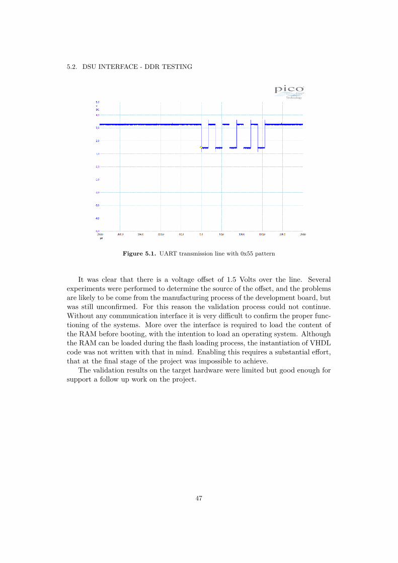
The DSU requires a synchronization pattern to establish a communication. Thecommunication process is started by the host PC, by sending the 0x55 pattern twoconsecutive times over the line. This is used by the DSU to infer the baudrate, andset the clock speed. To debug in a further effort an oscilloscope was used to inspectthe communication line. The results are depicted in the figure 5.1.
46
5.2. DSU INTERFACE - DDR TESTING
Figure 5.1. UART transmission line with 0x55 pattern
It was clear that there is a voltage offset of 1.5 Volts over the line. Severalexperiments were performed to determine the source of the offset, and the problemsare likely to be come from the manufacturing process of the development board, butwas still unconfirmed. For this reason the validation process could not continue.Without any communication interface it is very difficult to confirm the proper func-tioning of the systems. More over the interface is required to load the content ofthe RAM before booting, with the intention to load an operating system. Althoughthe RAM can be loaded during the flash loading process, the instantiation of VHDLcode was not written with that in mind. Enabling this requires a substantial effort,that at the final stage of the project was impossible to achieve.
The validation results on the target hardware were limited but good enough forsupport a follow up work on the project.
47

Part IV
A new core architecture’s exploration
49


Chapter 6
New CPU architecture for soft SoC inRTG4
As a side task for the main goal of the project, the comparison of the LEON2-FTwith a newer architecture is desirable. Of special interest for space applications anddue to the current trends in the industry, the candidate is a ARM CPU.
The Cortex-R series is specially designed by ARM to meet deterministic andhigh performance challenges, making the series a viable solution of real-time andreliability critical applications. Because of this and license availability an effort tolook at the CPUs side by side within the constraints of current soft SoC developingoptions was likely. The comparison is specially desirable with the new MDPA-DDR enhanced design. Although is important to highlight the fact that a directcomparison is not possible with the current results, then just a few aspects weretarget to evaluation, this is performance in terms of theoretical DMIPS and FPGAresources consumption.
In terms of microarchitecture the Cortex-R5 is a modern processor, and it in-cludes many features that the LEON2 lack. The Cortex-R5 microprocessor uses aARMv7-R microarchitecture, and among the features that the LEON2 misses thereis, instruction pre-fetch, branch prediction, dual-issue execution, parallel executionpaths for load-store, AXI bus interface, and dual-core configuration.
Due to all this the Cortex-R5 performance according to ARM is 1.67/2.02/2.45DMIPS/MHz. The three different values depends on how the Drystone benchmarkis executed. The performance is 1.67 DMIPS/MHz when following all of the groundrules laid out in the Dhrystone, 2.02 DMIPS/MHz when using inlining of functionsand 2.45 when allowing simultaneous multifile compilation.
On the other hand LEON2-FT known performance is 0.85 DMIPS/MHz (for anASIC implementation). Which means that the Cortex-R5 performs, in the worstcase, 1,96 times better, and it might perform 2,88 times faster under properly com-piled code. But the question is whether the Cortex-R5 can run at the same fre-quency that its simpler counterpart, or at a frequency that is no lower than half thefrequency of the LEON2-FT.
51
CHAPTER 6. NEW CPU ARCHITECTURE FOR SOFT SOC IN RTG4
The current work has showed that the LEON2-FT can run at 40 MHz whenimplemented in the RTG4 technology. Next the results of the synthesis of theCortex-R5 for the RTG4 technology are presented.
6.1 Main findingsThe SoC implementation with a Cortex-R5 core includes the following:
• One Cortex-R5 core, without floating point unit
• Network interconnect module
• CoreSightTM Subsytem module
• Watchdog module
• Vectorized interrupt controller
• UART interface
• One SpaceWire interface
• Reset and clock controller
• GPIO and PWM module
• Debug interface
• Military Bus interface
After synthesizing the SoC module the resources consumption in the RTG4 weregathered. All the logic elements consumed represent more than the total availableresources, and the math blocks necessary are several times the total in the RTG4.It is inconclusive if it is possible to fit the entire SoC in RTG4, but it is highlyunlikeable.
The critical path is one order or magnitude over the LEON2-FT one. Thecomplexity of the SoC when using a Cortex-R5 core increases dramatically, loweringthe frequency numbers,and this naturally lowers the performance.
The timing results are non conclusive neither, but acceptable frequencies werenever achieved. Considering the theoretical performance numbers, the implementedSoC need at least half of the frequency of the MDPA to overcome its performance.The results show that the RTG4 plays an important row when comparing both softSoC and impacts heavily the ability to achieve better numbers from the Cortex-R5CPU.
52
Part V
Final Part
53


Chapter 7
Future improvements and workproposals
After completing the present work, several opportunities to continue working leftfor future projects. Among those the following task can be listed.
1. Run the benchmarks on the target hardware. Due to the aforementionedproblems with the DSU interface no code was loaded in the main memories,by loading an operating system more information can be extracted on theperformance of the processor and shed a light on what other areas requireimprovement regarding the SoC microarchitecture.
2. Implement an Memory Management Unit (MMU) to increase the total mem-ory available. With the results achieved, the usage of more memory is possible,because the limited addressing of the 32 bits bus a MMU will be required inthe future to access memory spaces beyond the 4GB.
3. Reduce the waiting cycles of the internal RAM and ROM to 1. An effort stillcan be done to reduce the latency of the internal RAM. Finding the reasonsthat limit the waiting cycles to 1, and overcome those limits seems to befeasible, even though changes in the memory controller will be required
4. Fix the space wire, through floorplan constraints. It is of the uttermost im-portance to fix the Space Wire interface, no spaceborne component is usefulwithout that interface. The solution is the use floorplan constraints to guidethe place and route tool in the processes.
5. Improve the cache’s memory by directly implementing instead of inferring thememory. It is clear that infered memory is not the best option here, a lotof resources are wasted because of how the caches are connected. Changingthis implies changes in the LEON2 core, but if other components must theimplemented in the same FPGA, the effort worth the saved resources.
55

CHAPTER 7. FUTURE IMPROVEMENTS AND WORK PROPOSALS
6. Use more advance CPUs. Newer CPUs like LEON3 or LEON4 which aremore suitable to compete in terms of performance and modern features, canbe compared against the ARM implementations.
56

Chapter 8
Conclusions
DDR3 memory controller implementation was successful, the proposed architecturefor the SoC and its implementation was properly executed leading to key findingsand valuable information for future products. Even though only the verification pro-cess was fully completed and the validation stopped after finding problems with thedevelopment kit boards, the results are satisfactory considering the amount of workthat all the process requires. The DDR3 technology demonstrated to be a betteroption than implemented the RAM internally, showing that from the architecturalperspective is a great candidate for spaceborne missions.
When comparing the results against Virtex-V seems that the RTG4 has closenumbers in terms of timing and resources, but the RTG4 STMR-D flip flops featureis on, and the Virtex-V implementation is not using the TMR flip flops. This meansthat when choosing between these two FPGA technologies, the RTG4 provides twoadvantages. The extra reliability and the memory controller IP which expands thecapabilities of the SoC. Because of that, the RTG4 is a more attractive technologyfor future projects.
Cortex-R5 seems to require more resources than the ones available on the RTG4.If the resources problems are disregarded, the specification tells us that the Cortex-R5 matches or overcomes the LEON2-FT when using optimized code. But, mostprobably using optimized code is not good for safety critical applications. Additionalwhen considering the level of complexity and FPGA resources consumed in theFPGA matching or overcoming bit little the performance of the LEON2-FT CPUis simply not enough.
The implementation has potential to be used in future projects. The work doneincreases the knowledge and understanding of the potential usages of the new RTG4technology in spaceborne applications. This is a valuable outcome that can be usedby other when designing new products for the space electronics market.
57


Part VI
Appendix
59

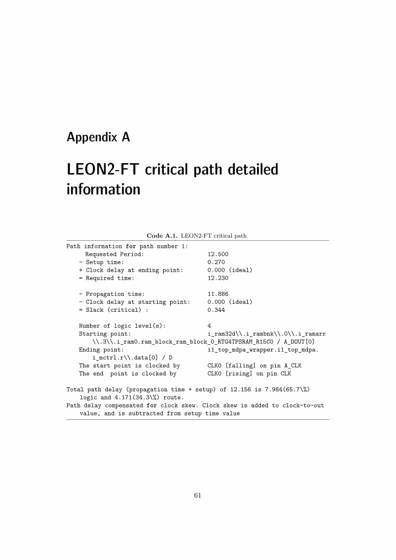
Appendix A
LEON2-FT critical path detailedinformation
Code A.1. LEON2-FT critical path
Path information for path number 1:Requested Period: 12.500
- Setup time: 0.270+ Clock delay at ending point: 0.000 (ideal)= Required time: 12.230
- Propagation time: 11.886- Clock delay at starting point: 0.000 (ideal)= Slack (critical) : 0.344
Number of logic level(s): 4Starting point: i_ram32d\\.i_rambnk\\.0\\.i_ramarr
\\.3\\.i_ram0.ram_block_ram_block_0_RTG4TPSRAM_R15C0 / A_DOUT[0]Ending point: i1_top_mdpa_wrapper.i1_top_mdpa.
i_mctrl.r\\.data[0] / DThe start point is clocked by CLK0 [falling] on pin A_CLKThe end point is clocked by CLK0 [rising] on pin CLK
Total path delay (propagation time + setup) of 12.156 is 7.984(65.7\%)logic and 4.171(34.3\%) route.
Path delay compensated for clock skew. Clock skew is added to clock-to-outvalue, and is subtracted from setup time value
61

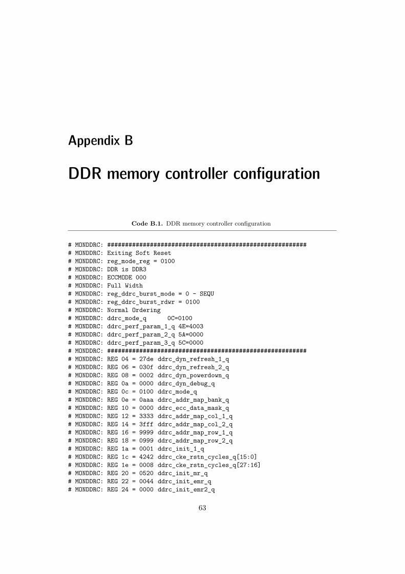
Appendix B
DDR memory controller configuration
Code B.1. DDR memory controller configuration
# MONDDRC: ######################################################### MONDDRC: Exiting Soft Reset# MONDDRC: reg_mode_reg = 0100# MONDDRC: DDR is DDR3# MONDDRC: ECCMODE 000# MONDDRC: Full Width# MONDDRC: reg_ddrc_burst_mode = 0 - SEQU# MONDDRC: reg_ddrc_burst_rdwr = 0100# MONDDRC: Normal Ordering# MONDDRC: ddrc_mode_q 0C=0100# MONDDRC: ddrc_perf_param_1_q 4E=4003# MONDDRC: ddrc_perf_param_2_q 5A=0000# MONDDRC: ddrc_perf_param_3_q 5C=0000# MONDDRC: ######################################################### MONDDRC: REG 04 = 27de ddrc_dyn_refresh_1_q# MONDDRC: REG 06 = 030f ddrc_dyn_refresh_2_q# MONDDRC: REG 08 = 0002 ddrc_dyn_powerdown_q# MONDDRC: REG 0a = 0000 ddrc_dyn_debug_q# MONDDRC: REG 0c = 0100 ddrc_mode_q# MONDDRC: REG 0e = 0aaa ddrc_addr_map_bank_q# MONDDRC: REG 10 = 0000 ddrc_ecc_data_mask_q# MONDDRC: REG 12 = 3333 ddrc_addr_map_col_1_q# MONDDRC: REG 14 = 3fff ddrc_addr_map_col_2_q# MONDDRC: REG 16 = 9999 ddrc_addr_map_row_1_q# MONDDRC: REG 18 = 0999 ddrc_addr_map_row_2_q# MONDDRC: REG 1a = 0001 ddrc_init_1_q# MONDDRC: REG 1c = 4242 ddrc_cke_rstn_cycles_q[15:0]# MONDDRC: REG 1e = 0008 ddrc_cke_rstn_cycles_q[27:16]# MONDDRC: REG 20 = 0520 ddrc_init_mr_q# MONDDRC: REG 22 = 0044 ddrc_init_emr_q# MONDDRC: REG 24 = 0000 ddrc_init_emr2_q
63
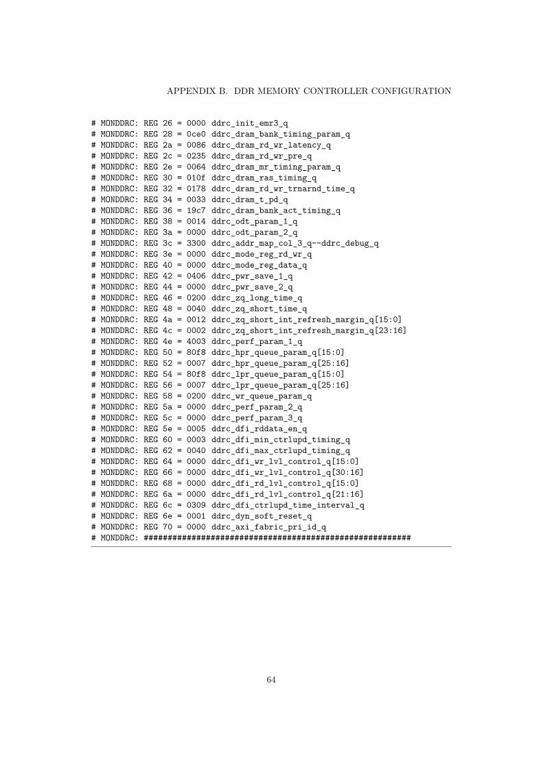
APPENDIX B. DDR MEMORY CONTROLLER CONFIGURATION
# MONDDRC: REG 26 = 0000 ddrc_init_emr3_q# MONDDRC: REG 28 = 0ce0 ddrc_dram_bank_timing_param_q# MONDDRC: REG 2a = 0086 ddrc_dram_rd_wr_latency_q# MONDDRC: REG 2c = 0235 ddrc_dram_rd_wr_pre_q# MONDDRC: REG 2e = 0064 ddrc_dram_mr_timing_param_q# MONDDRC: REG 30 = 010f ddrc_dram_ras_timing_q# MONDDRC: REG 32 = 0178 ddrc_dram_rd_wr_trnarnd_time_q# MONDDRC: REG 34 = 0033 ddrc_dram_t_pd_q# MONDDRC: REG 36 = 19c7 ddrc_dram_bank_act_timing_q# MONDDRC: REG 38 = 0014 ddrc_odt_param_1_q# MONDDRC: REG 3a = 0000 ddrc_odt_param_2_q# MONDDRC: REG 3c = 3300 ddrc_addr_map_col_3_q--ddrc_debug_q# MONDDRC: REG 3e = 0000 ddrc_mode_reg_rd_wr_q# MONDDRC: REG 40 = 0000 ddrc_mode_reg_data_q# MONDDRC: REG 42 = 0406 ddrc_pwr_save_1_q# MONDDRC: REG 44 = 0000 ddrc_pwr_save_2_q# MONDDRC: REG 46 = 0200 ddrc_zq_long_time_q# MONDDRC: REG 48 = 0040 ddrc_zq_short_time_q# MONDDRC: REG 4a = 0012 ddrc_zq_short_int_refresh_margin_q[15:0]# MONDDRC: REG 4c = 0002 ddrc_zq_short_int_refresh_margin_q[23:16]# MONDDRC: REG 4e = 4003 ddrc_perf_param_1_q# MONDDRC: REG 50 = 80f8 ddrc_hpr_queue_param_q[15:0]# MONDDRC: REG 52 = 0007 ddrc_hpr_queue_param_q[25:16]# MONDDRC: REG 54 = 80f8 ddrc_lpr_queue_param_q[15:0]# MONDDRC: REG 56 = 0007 ddrc_lpr_queue_param_q[25:16]# MONDDRC: REG 58 = 0200 ddrc_wr_queue_param_q# MONDDRC: REG 5a = 0000 ddrc_perf_param_2_q# MONDDRC: REG 5c = 0000 ddrc_perf_param_3_q# MONDDRC: REG 5e = 0005 ddrc_dfi_rddata_en_q# MONDDRC: REG 60 = 0003 ddrc_dfi_min_ctrlupd_timing_q# MONDDRC: REG 62 = 0040 ddrc_dfi_max_ctrlupd_timing_q# MONDDRC: REG 64 = 0000 ddrc_dfi_wr_lvl_control_q[15:0]# MONDDRC: REG 66 = 0000 ddrc_dfi_wr_lvl_control_q[30:16]# MONDDRC: REG 68 = 0000 ddrc_dfi_rd_lvl_control_q[15:0]# MONDDRC: REG 6a = 0000 ddrc_dfi_rd_lvl_control_q[21:16]# MONDDRC: REG 6c = 0309 ddrc_dfi_ctrlupd_time_interval_q# MONDDRC: REG 6e = 0001 ddrc_dyn_soft_reset_q# MONDDRC: REG 70 = 0000 ddrc_axi_fabric_pri_id_q# MONDDRC: ########################################################
64
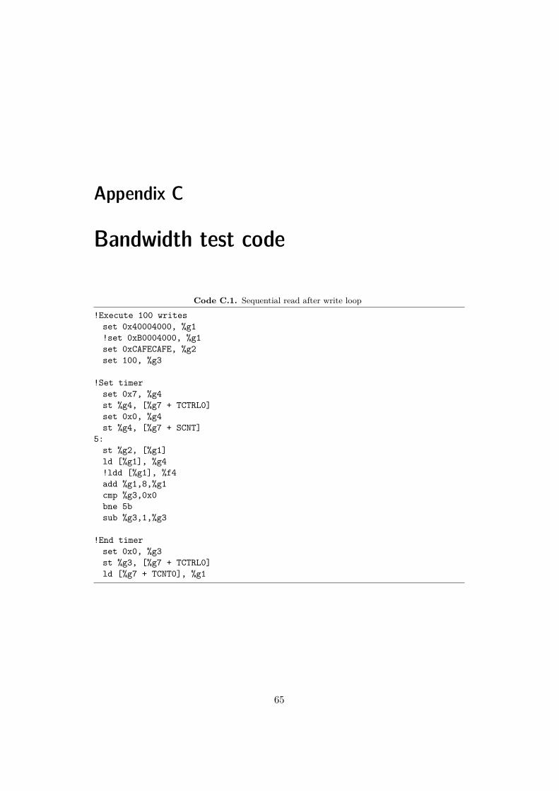
Appendix C
Bandwidth test code
Code C.1. Sequential read after write loop
!Execute 100 writesset 0x40004000, %g1!set 0xB0004000, %g1set 0xCAFECAFE, %g2set 100, %g3
!Set timerset 0x7, %g4st %g4, [%g7 + TCTRL0]set 0x0, %g4st %g4, [%g7 + SCNT]
5:st %g2, [%g1]ld [%g1], %g4!ldd [%g1], %f4add %g1,8,%g1cmp %g3,0x0bne 5bsub %g3,1,%g3
!End timerset 0x0, %g3st %g3, [%g7 + TCTRL0]ld [%g7 + TCNT0], %g1
65

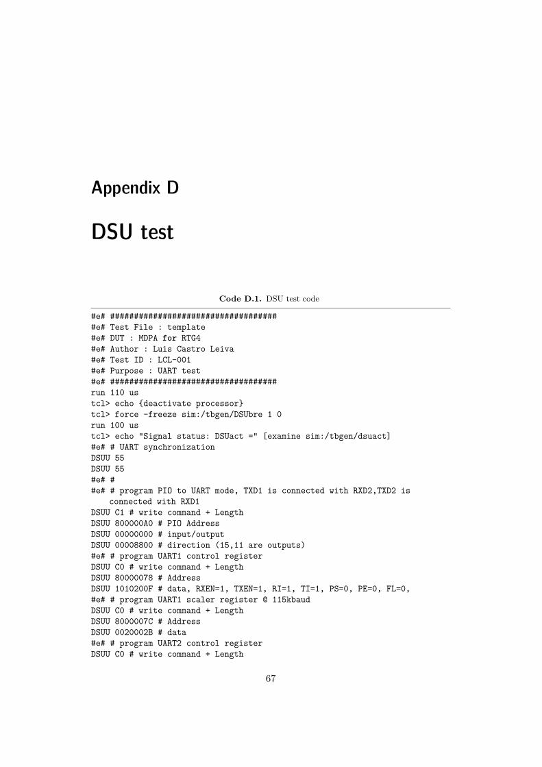
Appendix D
DSU test
Code D.1. DSU test code
#e# ####################################e# Test File : template#e# DUT : MDPA for RTG4#e# Author : Luis Castro Leiva#e# Test ID : LCL-001#e# Purpose : UART test#e# ###################################run 110 ustcl> echo {deactivate processor}tcl> force -freeze sim:/tbgen/DSUbre 1 0run 100 ustcl> echo "Signal status: DSUact =" [examine sim:/tbgen/dsuact]#e# # UART synchronizationDSUU 55DSUU 55#e# ##e# # program PIO to UART mode, TXD1 is connected with RXD2,TXD2 is
connected with RXD1DSUU C1 # write command + LengthDSUU 800000A0 # PIO AddressDSUU 00000000 # input/outputDSUU 00008800 # direction (15,11 are outputs)#e# # program UART1 control registerDSUU C0 # write command + LengthDSUU 80000078 # AddressDSUU 1010200F # data, RXEN=1, TXEN=1, RI=1, TI=1, PS=0, PE=0, FL=0,#e# # program UART1 scaler register @ 115kbaudDSUU C0 # write command + LengthDSUU 8000007C # AddressDSUU 0020002B # data#e# # program UART2 control registerDSUU C0 # write command + Length
67

APPENDIX D. DSU TEST
DSUU 80000088 # AddressDSUU 1010200F # data#e# # program UART2 scaler register @ 115kbaudDSUU C0 # write command + LengthDSUU 8000008C # AddressDSUU 0020002B # data#e# # send data over UART1 to UART 2DSUU C0 # write command + LengthDSUU 80000070 # AddressDSUU 000000AA # data#e# # send data over UART2 to UART 1DSUU C0 # write command + LengthDSUU 80000080 # AddressDSUU 000000CC # datarun 20 us#e# # Read UART Registers, confirm the configurationDSUU 87 # Read command + LengthDSUU 80000070 # Addressrun 10 usDSUU CP 000000CC # Receive Data at 0x80000070, data registerDSUU CP 00000886 # Receive Data at 0x80000074, status registerDSUU CP 1010200F # Receive Data at 0x80000078, control registerDSUU CP 0020002B # Receive Data at 0x8000007C, scaler registerDSUU CP 000000AA # Receive Data at 0x80000080, data registerDSUU CP 00000886 # Receive Data at 0x80000084, status registerDSUU CP 1010200F # Receive Data at 0x80000088, control registerDSUU CP 0020002B # Receive Data at 0x8000008C, scaler registerDSUU CP EOP<tcl>source ../../scripts/test_report.tclreport_testcase</tcl>END
68
Bibliography
[1] RTG4 – Latest Family of Radiation-Tolerant FPGAs from Microsemi | EETimes.
[2] European Space Agency. ESA - The AMBA bus system. http://www.esa.int/Our_Activities/Space_Engineering_Technology/Microelectronics/The_AMBA_Bus_System. Accessed: 2017-07-05.
[3] ARM Inc. ARM7TDMI Technical Reference Manual, 1 2001.
[4] Atmel Corporation. Rad-Hard 32 bit SPARC V8 Processor, 8 2011. Rev. G.
[5] Niccolò Battezzati, Luca Sterpone, and Massimo Violante. Reconfigurable fieldprogrammable gate arrays for mission-critical applications. Springer Science &Business Media, 2010.
[6] Robert C Baumann. Radiation-induced soft errors in advanced semiconductortechnologies. IEEE Transactions on Device and materials reliability, 5(3):305–316, 2005.
[7] ECSS Secretariat ESA-ESTEC Requirements & Standards Division.Spacewire - links, nodes, routers and networks - ECSS-E-ST-50-12C, 2008.
[8] ESA. LEON2-FT - HDL. http://www.esa.int/Our_Activities/Space_Engineering_Technology/Microelectronics/LEON2-FT_-_HDL. Accessed:2017-06-19.
[9] Jiri Gaisler. A portable and fault-tolerant microprocessor based on the sparcv8 architecture. In Proceedings of the International Conference on DependableSystems and Networks (DSN‘02), pages 409–415. IEEE, 2002.
[10] Eberhard Gill. Comparison of the performance of microprocessors for space-based navigation applications. Space Flight Technology, German Space Opera-tions Center (GSOC), TN, pages 05–02, 2005.
[11] Reno Harboe-SØrensen, F-X Guerre, and G Lewis. Heavy-ion see test con-cept and results for ddr-ii memories. IEEE Transactions on Nuclear Science,54(6):2125–2130, 2007.
69
BIBLIOGRAPHY
[12] Martin Herrmann, Kai Grürmann, Fritz Gliem, Hagen Schmidt, Michele Mus-chitiello, and Véronique Ferlet-Cavrois. New see and tid test results for 2-gbitand 4-gbit ddr3 sdram devices. In Radiation and Its Effects on Componentsand Systems (RADECS), 2013 14th European Conference on, pages 1–5. IEEE,2013.
[13] Martin Herrmann, Grürmann Kai, Gliem Fritz, Kettunen Heikki, and Ferlet-Cavrois Véronique. Heavy ion see test of 2 gbit ddr3 sdram. In Radiationand Its Effects on Components and Systems (RADECS), 2011 12th EuropeanConference on, pages 934–937. IEEE, 2011.
[14] ARM Inc. AMBA specification, revision 2, 1999.
[15] SPARC International Inc. The SPARC architecture manual, version 8, 1992.
[16] Fernanda Kastensmidt and Paolo Rech. FPGAs and parallel architectures foraerospace applications: soft errors and fault-tolerant design. Springer, 2015.
[17] Ian Kuon and Jonathan Rose. Measuring the gap between fpgas and asics.IEEE Transactions on computer-aided design of integrated circuits and systems,26(2):203–215, 2007.
[18] RL Ladbury, MD Berg, EP Wilcox, KA LaBel, HS Kim, AM Phan, andCM Seidleck. Use of commercial fpga-based evaluation boards for single-eventtesting of ddr2 and ddr3 sdrams. IEEE Transactions on Nuclear Science,60(6):4457–4463, 2013.
[19] Joseph R Marshall. Evolution and applications of system on a chip spacewirecomponents for spaceborne missions. In 2nd International SpaceWire Confer-ence, Nara, Japan, 2008.
[20] Microsemi. Mitigation of radiation effects in rtg4 radiation - tolerant flashfpgas, 2015.
[21] Microsemi. RTG4 FPGA Clocking Resources - User Guide - UG0586, 2017.
[22] Microsemi. RTG4 FPGA DDR Memory Controller - User Guide - UG0573,2017.
[23] Microsemi. RTG4 FPGA Fabric - User Guide - UG0574, 2017.
[24] Shubhendu S Mukherjee, Joel Emer, and Steven K Reinhardt. The soft errorproblem: An architectural perspective. In High-Performance Computer Ar-chitecture, 2005. HPCA-11. 11th International Symposium on, pages 243–247.IEEE, 2005.
[25] Jiri Gaisler Gaisler Research. The LEON2-FT Processor User’s Manual, 2007.
70
BIBLIOGRAPHY
[26] Ronald Donald Schrimpf and Dan M Fleetwood. Radiation effects and softerrors in integrated circuits and electronic devices, volume 34. World Scientific,2004.
[27] Helder Silva, José Sousa, Daniel Freitas, Sergio Faustino, Alexandre Con-stantino, and Manuel Coutinho. Rtems improvement-space qualification ofrtems executive. 1st Simpósio de Informática-INFORUM, University of Lis-bon, 2009.
[28] Reinhold P Weicker. Dhrystone: a synthetic systems programming benchmark.Communications of the ACM, 27(10):1013–1030, 1984.
[29] Reinhold P Weicker. Dhrystone benchmark: rationale for version 2 and mea-surement rules. ACM SIGPLAn notices, 23(8):49–62, 1988.
[30] Roland Weigand. ESA microprocessor develop-ment. http://microelectronics.esa.int/papers/DASIA2011-ESA-Microprocessors-RolandWeigand-Slides.pdf. Accessed:2017-07-05.
[31] Richard York. Benchmarking in context: Dhrystone. ARM, March, 2002.
71


TRITA TRITA-ICT-EX-2017:135
www.kth.se