journal of materials chemistry a perovskite... · tolerance factor (t) and octahedral factor (m),...
TRANSCRIPT
Journal ofMaterials Chemistry A
REVIEW
Publ
ishe
d on
30
Aug
ust 2
019.
Dow
nloa
ded
by Z
hejia
ng U
nive
rsity
on
10/3
/201
9 11
:50:
33 A
M.
View Article OnlineView Journal | View Issue
Inorganic perovs
aInstitute of New Energy Technology, Colleg
Jinan University, Guangzhou 510632, PR ChbKey Laboratory of Micro-nano Electronic
Province, College of Information Science
University, Hangzhou, China
Cite this: J. Mater. Chem. A, 2019, 7,21036
Received 24th June 2019Accepted 30th August 2019
DOI: 10.1039/c9ta06674h
rsc.li/materials-a
21036 | J. Mater. Chem. A, 2019, 7, 210
kite solar cells: an emergingmember of the photovoltaic community
Jialong Duan, a Hongzhe Xu,a W. E. I. Sha, b Yuanyuan Zhao, a Yudi Wang,a
Xiya Yang a and Qunwei Tang *a
Perovskite solar cells (PSCs) have attracted tremendous interest because of their rapid improvement in
power conversion efficiency (PCE) from the initial PCE of 3.8% for the first prototype to the certified PCE
of 25.2% in 2019. However, the inherent chemical instability of organic–inorganic hybrid perovskite
halides influenced by moisture, heat and ultraviolet light is still a critical issue for them to meet
application-specific requirements owing to the weak-bonded organic components in the hybrid crystal
structure. The use of all-inorganic perovskites CsPbI3�xBrx (x ¼ 0, 1, 2, and 3) as light-harvesters by
completely substituting organic species with inorganic Cs+ ions has been recently regarded as
a promising solar conversion technology. Since the initial efficiency of 2.9% achieved in 2015, the highest
PCE record for inorganic PSCs has risen to 18.4% through structure optimization, compositional
engineering, interfacial engineering, solvent control and surface passivation, etc. This article is dedicated
to providing an up-to-date review on the development of inorganic PSCs tailored by various inorganic
perovskite materials with gradually changed optical properties and stability, as well as the film-making
methods and interfacial engineering technologies. Their limited efficiencies in theory and recombination
mechanisms are also predicted with a detailed balance model. Finally, we focused on the state-of-the-
art strategies for enhancing the photovoltaic performance and identified new challenges and outlooks
for future studies in this field.
1. Introduction
Solar radiation releases enormous solar energy, accounting foralmost 99% of the total energy in the earth. Therefore, the har-vesting of solar energy by energy-conversion devices (i.e., photo-voltaics or solar cells) is regarded as a promising solution toaddress the energy and environmental problems. It has beenalways a hot topic to convert solar energy into electricity bycomplicated photoelectrical or photoelectrochemical principlessince the discovery of the rst solar panel in 1954.1,2 To date,photovoltaics can be divided into three categories according tothe photovoltaic materials: (i) crystalline silicon solar cells, (ii)thin-lm technologies, and (iii) the emerging solar cells. Asemerging photovoltaics in recent decades, dye-sensitized solarcells (DSSCs),3–10 organic solar cells (OSCs),11–22 quantum dot-sensitized solar cells (QDSCs),23–30 and perovskite solar cells(PSCs)31–37 are regarded as promising candidates due to theirremarkable power conversion efficiency (PCE) enhancement andlow production costs. Since 2009, organic–inorganic hybridperovskite light-harvesters have been well-studied in theory,
e of Information Science and Technology,
ina. E-mail: [email protected]
Devices and Smart Systems of Zhejiang
and Electronic Engineering, Zhejiang
36–21068
experiment and module production, and the corresponding PSCshave seen a rapid rise in PCE from 3.8% to 25.2% within tenyears.38–47 These hybrid PSCs are always highlighted by somesuperiorities: (1) the bandgap of CH3NH3PbI3 (MAPbI3, 1.55 eV) orCH(NH2)2PbI3 (FAPbI3, 1.43 eV) is highly suited for wide-spectralphotovoltaics;48,49 (2) the hybrid perovskites present high extinc-tion coefficient and incident-photon-to-current conversion effi-ciency (IPCE) in devices;40 (3) the carrier diffusion length is long inperovskite lms.50,51 Science Daily said “There is now an urgentneed to tackle the threat of climate change resulting fromhumanity's overreliance on fossil fuel, and the rapid developmentof new solar technologies must be part of the plan.” Large area,improved stability, high efficiency, and good reproducibility arethe critical competitive elements to assess the commercialapplication of PSCs. Although the state-of-the-art organic–inor-ganic hybrid PSCs have comparable PCEs to silicon solar cells,organic–inorganic hybrid perovskite lms generally suffer fromcompositional degradation and crystallization destruction underpersistent attack by heat, moisture, or ultraviolet (UV) light,52,53
mainly arising from the inherent instability of organic volatilecomponents, such asMA+ and FA+, in thermal and UV conditions.Furthermore, organicMA+ and FA+ species are prone to react withwater molecules or under sunlight and thermal conditions toform intermediate hydrates, which can lead to serious perovskitedegradation and therefore poor device lifetime.54–57
This journal is © The Royal Society of Chemistry 2019

Fig. 1 The best efficiencies for various inorganic PSCs.
Fig. 2 Unit cell structure of an inorganic CsMX3 perovskite.70
Review Journal of Materials Chemistry A
Publ
ishe
d on
30
Aug
ust 2
019.
Dow
nloa
ded
by Z
hejia
ng U
nive
rsity
on
10/3
/201
9 11
:50:
33 A
M.
View Article Online
In recent works, the substitution of organic counterpartswith inorganic cesium cations (Cs+) is considered an effectiveapproach to improve the environmental tolerance of perovskitelms under harsh conditions.58,59 Full-cesium perovskites havebeen demonstrated to possess high hole mobility (�520 cm2 Vs�1) and electron mobility (�530 cm2 V s�1) when obtainedfrom the cold-pressed pellets of annealed CsSnI3 polycrystallinematerial, while an electron lifetime of 2.5 ms and an estimatedelectron mobility of�1000 cm2 V s�1 were obtained for CsPbBr3halide single-crystals.60,61 Based on these properties, it can bepredicted that inorganic perovskites may be another candidateas a light absorber. Since the initial report for fully inorganiccesium lead halides in 1893 and subsequent systematic studiesin this eld,62–69 these perovskite halides have been successfullyassembled into inorganic PSCs in 2015. To date, enormousefforts have beenmade to advance the PCE of inorganic devices,Fig. 1 plots the maximized PCEs of inorganic PSCs with CsPbI3,CsPbI2Br, CsPbIBr2, or CsPbBr3 as light absorbers, where theinitial PCEs are all lower than 5% but the maximized value todate is more than 18%, thus demonstrating the great potentialfor their application in the future. In this review, we summarizethe recent advances of all-inorganic PSCs by emphasizing theirstructural phase transformation, tunable optoelectronic prop-erties, environmental stability, lm-making methods, interfa-cial engineering, and their limited efficiency, as well as thechallenges still faced by scientists and their future outlooks.
2. Fundamental background2.1 Crystal structures of inorganic perovskites
The chemical formula ABX3 [A (+1), B (+2), X (�1)] is alwaysdesignated for perovskite-structured materials with a similarcrystal structure to the mineral CaTiO3. The recently emergingall-inorganic perovskites can also be described by a similarchemical formula CsMX3 (M ¼ Pb2+ or Sn2+, X ¼ I� or Br�),where Cs+ occupies a corner of a unit cell with 12-fold coor-dination, M is a divalent metal cation in general sitting ina body-centered position with 6-fold coordination, and X isa halogen with a face-centred position, as depicted in Fig. 2.70
This journal is © The Royal Society of Chemistry 2019
There is a lower energy barrier for the intercalation of CsXinto PbBr2 frameworks during perovskite formation,71 arisingfrom the smaller ionic radius of Cs+ (1.81 A for Cs+) than 2.70 Afor MA+ and 2.79 A for FA+. The crystal structure of the perov-skite is adjustable in terms of its composition by controlling thetolerance factor (t) and octahedral factor (m), as proposed byGoldschmidt, in a rational range. Here, t indicates the state ofdistortion and stability of perovskite structures, and this valuecan be obtained according to the following formula:72
t ¼ ðrA þ rXÞ=ffiffiffi2
p ðrB þ rXÞ, where r represents the ionic radius ofatoms of A, B, and X sites, respectively, m is dened as a rB/rXratio, which is directly correlated to the formation of a BX6
octahedron.25,73,74 Both t and m are used to predict the form-ability of a perovskite structure. Typically, stable 3D halideperovskite crystals can be formed under the condition of 0.81 < t< 1.0 and 0.44 < m < 0.90, an ideal cubic perovskite structure at0.9 < t < 1.0, and a tetragonal or orthorhombic structure in therange of 0.81 < t < 0.9, respectively.75,76 When t > 1.0, a NH4CdI3-type crystal structure is usually favored. When t < 0.8, a CsNiBr3-type crystal structure is most likely to form.77 Taking the crystalrestrictions, such as the t range and ionic radius of the
commonly used Pb2+ (1.2 A), Br� (1.96 A) and I� (2.2 A) ions intoconsiderations, the ionic radius of the A-site ion should be
limited to 2.9 A. Otherwise, the cubic structure will be distortedand the crystal symmetry will be reduced, leading to forming anunsatisfactory crystal with notorious photovoltaic performanceor long-term stability. So the inorganic cations with Cs+ or Rb+
cations could lead to a more favorable tolerance factor tofacilitate the stabilization of the photoactive perovskite phase ina broader temperature range and to improve their thermal andlight soaking stability.
2.2 Stability of inorganic perovskites
The degradation mechanisms of organic–inorganic hybridperovskites have been widely explored during the past severalyears. Organic cations, such as MA+ in MAPbI3, have acidicprotons; therefore, the perovskite degradation will be initiatedby the reaction between the superoxide and methylammonium
J. Mater. Chem. A, 2019, 7, 21036–21068 | 21037

Journal of Materials Chemistry A Review
Publ
ishe
d on
30
Aug
ust 2
019.
Dow
nloa
ded
by Z
hejia
ng U
nive
rsity
on
10/3
/201
9 11
:50:
33 A
M.
View Article Online
moiety under light and oxygen conditions.78 In this fashion, theuse of all-inorganic perovskites free of organic species canimprove the tolerance of the perovskite crystal to oxygen andlight. Unfortunately, such inorganic perovskites have beendemonstrated to be not stable enough under external stimuli,such as moisture, light, heat, and oxygen. To the best of ourknowledge, CsPbBr3 has the most superior stability among thedifferent inorganic perovskites, while the I-containing perov-skites display inferior long-term stability. Different from hybridperovskites, the inorganic perovskites are free of hygroscopicorganic cations, which are responsible for the hydration-induced degradation. Therefore, polymorphic transition,decomposition, oxidation, or their combinations may be theintrinsic origins of their instability properties.77 For the state-of-the-art CsPbI3 inorganic perovskite, the phase instability ismainly due to transitions between the desirable photoactiveperovskite black phase and the undesirable non-perovskiteyellow phase, although transition to the yellow phase isreversible, attributed to the undesirable tolerance factor.Although the polymorphic transition can be signicantly sup-pressed via increasing the Br dosage (producing a more stabi-lized structure with t > 0.8 and m > 0.4), halide segregation maybe another issue for the performance degradation under light oran electron beam, especially for perovskites with an I dosagelower than 40%. Based on the above-mentioned discussion, itcan be seen that the phase instability of CsPbX3 can be mainlyattributed to the polymorphic transition. There are also otherinorganic perovskite materials, such as CsSnX3 and CsGeX3,where the facile oxidation of Sn2+/Ge2+ to Sn4+/Ge4+ in ambientair results in a sluggish efficiency and rapid performancedegradation, which will be discussed in the following part.
2.3 Inorganic PSC architectures
Similar to hybrid PSCs, the state-of-the-art all-inorganic devicesare generally constructed in a regular n–i–p or inverted p–i–narchitectures, as shown in Fig. 3a and c, in which both perov-skite layers are sandwiched between an n-type electron-transporting layer (ETL) and a p-type hole-transporting layer(HTL). A mesoporous scaffold, either semiconducting or insu-lating, is also generally included, as shown in Fig. 3b. Inphysics, the light absorption of a perovskite is a light–matterinteraction process, in which the electrons in the interactingmaterials resonate with the electric eld of the irradiatingoptical signal and induce polarization. The working principle of
Fig. 3 Device structures of typical PSCs.
21038 | J. Mater. Chem. A, 2019, 7, 21036–21068
a typical PSC is based on the photovoltaic effect of a p–n junc-tion, and the built-in potential is formed at p–n junctions. Uponsunlight irradiation, the atoms in an inorganic perovskiteabsorb photons to release electrons and subsequently generateelectron–hole pairs. The photo-induced electrons are driven toan n-type region and holes are driven to a p-type region underthis barrier electric eld, and therefore, a photogeneratedelectric eld opposite to the direction of the barrier electric eldis formed near p–n junctions. Part of the photogenerated elec-tric eld counteracts the barrier electric eld and the rest causeselectromotive force in the thin layer between the n-type and p-type regions to realize electric power output through anexternal circuit. In this fashion, the intrinsic mechanism forregular n–i–p or inverted p–i–n architectures is identical exceptfor the charge-carrier transfer direction.
Considering the morphology of a transparent conductiveoxide (TCO)-attached charge-contact layer, a mesoporous orplanar architecture can be visibly distinguished. To date, bothstructured PSCs have achieved a high efficiency over 20% basedon a hybrid perovskite layer, demonstrating great potential inreal application.79,80 The choice of whether to fabricate a meso-porous or planar architecture is highly dependent on theperovskite lm quality and properties. For mesoporous PSCsderived from dye-sensitized solar cells,81 the perovskite layercan be inltrated within the scaffold via the interconnectedchannels, resulting in a facile and reproducible device fab-rication.82,83a,b The concept of a planar device originates fromTiO2- or Al2O3-based mesoporous PSCs.43 In detail, a planararchitecture is implemented on a compact charge-transfer layerwithout pores, on which it is more facile to deposit a perovskitelm through vapor-based technologies, which will be discussedin Section 5. Compared to mesoporous devices, the high-qualityand smoother perovskite layer plays an important role inobtaining a satisfactory solar-to-electric conversion efficiency.In fact, a much higher photocurrent or photovoltage can berealized based on a planar architecture, but it will suffer frommuch worse hysteresis, which may arise from insufficientcharge extraction rates, therefore leading to chargeaccumulation.
3. Inorganic perovskites solar cells
Are organic cations essential for high-efficiency PSCs? Thisurgent question was analyzed by Hodes and Snaith in 2015,although the rst report on inorganic CsPbX3 crystal data can be
This journal is © The Royal Society of Chemistry 2019

Review Journal of Materials Chemistry A
Publ
ishe
d on
30
Aug
ust 2
019.
Dow
nloa
ded
by Z
hejia
ng U
nive
rsity
on
10/3
/201
9 11
:50:
33 A
M.
View Article Online
traced back to 1893.62,84,85 Hodes et al. demonstrated that theorganic cations are not indispensable for high open-circuitvoltage (Voc) PSCs through comparing hybrid organic–inor-ganic methylammonium lead bromide (MAPbBr3) and all-inorganic cesium lead bromide (CsPbBr3) with differentHTLs.84 Through identifying the possible fundamental differ-ences in their structural, thermal, and electronic characteris-tics, they found that a large Voc prots from the presence ofa direct optical bandgap of around 2.3 eV. Simultaneously, theCsPbBr3 halide had higher thermal stability than MAPbBr3.However, its large bandgap limited the PCE enhancement ofthis type of device. Snaith and co-workers fabricated a CsPbI3-based PSC for the rst time via a low-temperature phase tran-sition process at room temperature, achieving a PCE of 2.9%.85
Those works identify that the organic cation is not necessaryand this paved the way for further developments of much morethermally stable inorganic perovskites as light absorbers. In thissection, the state-of-the-art advances of all-inorganic PSCsengineered from compositional, doping, interfacial, and spec-tral aspects are systematically demonstrated, and the photo-voltaic parameters of typical devices based on various inorganicperovskites are summarized in Table 1.
3.1 Pb-based perovskites
CsPbX3 (X ¼ Br, I, with stoichiometric ratios of 0 : 3, 1 : 2, 2 : 1,and 3 : 0) materials can generally form a cubic phase perovskitestructure with intrinsic Goldschmidt's values for the tolerancefactor t ¼ 0.83–0.84. Inorganic perovskites possess ambipolarbehaviors, accompanying unique crystal structures, highabsorption coefficients, large exciton diffusion lengths, andexcellent charge-transporting properties, indicating that theycan cumulatively work as light absorbers and carrier conduc-tors.145 According to the above-mentioned properties, perovskitelms with a thickness of several hundreds of nanometers areenough to realize efficient solar-to-electric conversion.146–148
CsPbBr3- and CsPbI3-based solar cell models are two types ofdevices that were rst fabricated in the early stage of all-inorganic PSCs development. However, CsPbBr3 is limited byits narrow absorption range and CsPbI3 has thermodynamicphase instability in high-humidity (even in low temperaturewith zero humidity) and/or high-temperature conditions. Topursue a long-time prosperity for devices, scientists pay greatattention and made many innovations to try to overcome theseweakness, including tuning the Br : I ratio and doping foreignelements by compositional engineering to modulate the crystalstructure, absorption range, and durability.111,149,150 These nd-ings have led to the further exploration of many new congu-rations and derivative materials for CsPbX3.149,151 Fig. 4a showsthe absorption spectra evolution of CsPbI3�xBrx perovskiteswith various Br dosages, referring to an absorbance onsetchanging from 540 nm for CsPbBr3 to 718 nm for CsPbI3.111 Indetail, there is a linear relationship between the absorptiononset values and Br concentration in inorganic perovskites, asshown in Fig. 4b. In this fashion, the light-harvesting ability ofCsPbI3�xBrx perovskite can be precisely predicted, givinga possibility to obtain an ideal inorganic perovskite material
This journal is © The Royal Society of Chemistry 2019
with considerable long-term stability and photovoltaic proper-ties. To date, CsPbI3, CsPbI2Br, CsPbIBr2, and CsPbBr3 lms arethe main four types of state-of-the-art inorganic perovskites andtheir Shockley–Queisser (S–Q) limit efficiencies are 28.9%,24.4%, 22.1%, and 15.9% in photovoltaic devices, respectively.As shown in Fig. 4c, all the perovskites can form a typicalperovskite phase with diffraction peaks at around 14.62�,20.65�, and 28.94�, corresponding to the (100), (110), and (200)planes, respectively. These characteristic peaks shi to higherangles with increasing the Br dosage owing to the contraction ofthe crystal lattice upon the partial substitution of I atoms withBr atoms. From the external quantum efficiency (EQE) charac-terizations (Fig. 4d), it can be seen that the light response rangecan be extended to 620 nm (2.05 eV for CsPbIBr2), 700 nm(1.9 eV for CsPbI2Br), and then 740 nm (1.73 eV for CsPbI3) from540 nm (2.3 eV for CsPbBr3), in accordance with the absorptionspectra. It should be noted that the high trap-state density fromthe thermal dynamical instability of the black a-CsPbI3 perov-skite phase to the d-CsPbI3 non-perovskite phase delivers thelowest PCE and EQE values in the early stage.111
A high PCE and improved stability are equally signicant topromote the commercialization of all-inorganic PSCs. However,the light-harvesting ability and their tolerance to the environ-ment of these inorganic perovskites in ambient conditions isdramatically adverse. As shown in Fig. 4e, the normalizedphotovoltaic performance of the corresponding device degradessignicantly following the order of CsPbI3 > CsPbI2Br >CsPbIBr2 > CsPbBr3, demonstrating the incompatible power outability and long-term stability. While CsPbBr3 perovskite isrelatively stable without changes in either color or shape in 40%RH and 25 �C over 3 h as shown in Fig. 4f, CsPbIBr2, CsPbI2Br,and CsPbI3 present rapid decomposition by moisture attack.Therefore, how to simultaneously compromise the light-harvesting ability and stability is a great challenge in the eldof inorganic PSCs.
To better understand the properties of light absorbers, whichis crucial for the fabrication of high-performance inorganicPSCs, we summarize various Pb-based inorganic perovskitematerials that have been used as photoactive layers in thissection.
3.1.1 CsPbBr3. Early work on CsPbBr3, which presents anorthorhombic phase at room temperature and transforms toa tetragonal phase at 88 �C and to the “orange” cubic perovskitephase at 130 �C, was pioneered by Wells in 1893,62 but did notattract much more concerns until the early 21st century. Itsestimated electron mobility was reported to be as high as�1000cm2 V s�1 with an electron lifetime of 2.5 ms,61 which were alsocross-checked by Ghosh.152 From those excellent parameters, itis clear that the charge carrier within CsPbBr3 has greatpotential to obtain long diffusion or dri lengths to ensurea sufficient thickness of perovskite lm to suit photovoltaicdevices.
One of the outstanding properties of inorganic CsPbBr3-based PSCs is their high open-circuit voltage owing to pos-sessing a semiconductor bandgap of 2.3 eV (optical absorptionrange of 300–540 nm), as shown in Fig. 5a. Hodes et al.employed CsPbBr3 as a light harvester to fabricate a typical
J. Mater. Chem. A, 2019, 7, 21036–21068 | 21039

Table 1 Summary of device performances for various inorganic PSCs
Formula Device structures PCE Operation conditions Ref.
CsPbBr3 FTO/m-TiO2/CsPbBr3/Au 5.47% Ambient 84FTO/m-TiO2/CsPbBr3/Spiro-OMeTAD/Au 4.98% Ambient 84FTO/m-TiO2/CsPbBr3/CBP/Au 4.92% Ambient 84FTO/m-TiO2/CsPbBr3/PTAA/Au 5.72% Ambient 84FTO/m-TiO2/CsPbBr3/C 5.0% Ambient 86FTO/c-TiO2/m-TiO2/CsPbBr3/C 5.38% Ambient 87FTO/c-TiO2/m-TiO2/CsPbBr3/C 6.7% Ambient 88FTO/c-TiO2/m-TiO2/GQDs/CsPbBr3/C 9.72% Ambient 89FTO/c-TiO2/m-TiO2/Cs0.91Rb0.09PbBr3/C 9.86% Ambient 90FTO/c-TiO2/m-TiO2/CQDs/CsPbBr3/C 7.86% Ambient 91FTO/c-TiO2/m-TiO2/CsPbBr3/CuInS2–ZnS QDs/C 8.42% Ambient 92FTO/c-TiO2/m-TiO2/CQDs/CsPbBr3/PQDs/C 7.93% Ambient 93FTO/c-TiO2/m-TiO2/CQDs/CsPbBr3/RPQDs/C 8.2% Ambient 94FTO/c-TiO2/m-TiO2/CsPbBr3/CsSnBr3�xIx QDs/C 9.13% Ambient 95FTO/c-TiO2/m-TiO2/CsPbBr3–CsPb2Br5/Spiro-OMeTAD/Ag 8.36% Ambient 96FTO/c-TiO2/m-TiO2/CsPb0.97Sm0.03Br3/carbon 10.14% Ambient 97FTO/TiO2/CsPbBr3/MoS2/carbon 6.8% Ambient 98FTO/c-TiO2/m-TiO2/CsPbBr3/CsMBr3/C 10.6% Ambient 99FTO/c-TiO2/m-TiO2/CsPbBr3/ZnS:SnS/C 10.26% Ambient 100FTO/c-TiO2/CsPbBr3/CsPbBr3–CsPb2Br5/CsPbBr3–Cs4PbBr6/carbon 10.17% Ambient 101FTO/c-TiO2/m-TiO2/CsPbBr3/MnS/C 10.45% Ambient 102FTO/c-TiO2/CsPbBr3/Spiro-OMeTAD/Ag 10.91% Ambient 103
CsPbIBr2 FTO/m-TiO2/CsPbIBr2/Au 4.7% Glovebox 104FTO/bl-TiO2/mp-TiO2/CsPbIBr2/Spiro-OMeTAD/Au 6.3% Ambient 105FTO/NiOx/CsPbIBr2/MoOx/Au 5.52% N2 106FTO/c-TiO2/m-TiO2/CsPbIBr2/C 8.25% Ambient 70FTO/c-TiO2/m-TiO2/CsPb0.9Sn0.1IBr2/C 11.33% Ambient 70ITO/SnO2/CsPbIBr2/Spiro-OMeTAD/Ag 9.68% Ambient 107FTO/TiO2/CsBr/CsPbIBr2/C 10.71% Ambient 108ITO/SnO2/C60/CsPb1�xSnxIBr2/Spiro-OMeTAD/Au 11.53% Glovebox 109
CsPbI2Br ITO/SnO2/CsPbI2Br/PTAA/MoO3/Al 13.8% N2 110FTO/c-TiO2/CsPbI2Br/Spiro-OMeTAD/Ag 10.99% N2 111FTO/c-TiO2/CsPbI2Br/Spiro:Li-TFSi-tBP/Ag 10.3% N2 112FTO/c-TiO2/m-TiO2/CsPb0.98Sr0.02I2Br/P3HT/Au 11.3% N2 113FTO/bl-TiO2/Cs0.925K0.075PbI2Br/Spiro:Li-TFSi-tBP/Au 10.0% 20 �C, RH < 20% 114ITO/Ca/C60/CsPbI2Br/TAPC/TAPC:MoO3/Ag 11.8% Vacuum 115FTO/TiO2/CsPb0.98Mn0.02I2Br/CsPbI2Br QDs/PTAA/Au 13.47% N2 116ITO/SnO2/ZnO/CsPbI2Br/Spiro-OMeTAD/MoO3/Ag 14.6% N2 117ITO/c-TiO2/CsPbBrI2/Spiro-OMeTAD/Ag 10.34% N2 118FTO/TiO2/CsPbI2Br(3D–2D–0D)/PTAA/Au 12.39% Ambient 119FTO/NiOx/CsPbI2Br/ZnO@C60/Ag 13.3% Ambient 120ITO/c-TiO2/CsPbI2Br/Spiro-OMeTAD/Au 9.08% N2 121ITO/c-TiO2/CsPbI2Br/P3HT/Au 12.02% Ambient 122FTO/TiO2/CsPbI2Br/CsPbI3 QDs/PTAA/Au 14.45% Ambient 123ITO/c-TiO2/CsPbI2Br/Spiro-OMeTAD/Au 16.07% Glovebox 124FTO/c-TiO2/m-TiO2/BaI2:CsPbI2Br/P3HT/Au 14.85% Ambient 125FTO/c-TiO2/CsPb0.9Zn0.1I2Br/Spiro-OMeTAD/Ag 13.6% N2 126ITO/SnO2/CsPbI2Br/CsBr/Spiro-OMeTAD/Au 16.37% N2 glovebox 127
CsPbI3 FTO/c-TiO2/CsPbI3 QDs/Spiro-OMeTAD/MoOx/Al 10.77% Dry ambient condition 128FTO/c-TiO2/CsPbI3/CuI/Au 13.21% N2 129FTO/c-TiO2/CsPbI3/P3HT/Au 10.5% N2 130FTO/bl-TiO2/mp-TiO2/CsPbI3/P3HT/MoO3/Au 4.68% N2 131FTO/c-TiO2/CsPbI3/0.025EDAPbI4/Spiro-OMeTAD/Ag 11.8% N2 132FTO/TiO2/a-CsPbI3/Spiro-OMeTAD/Ag 4.13% Ambient 133ITO/PTAA/CsPbI3/PCBM/C60/BCP/Al 11.4% Glovebox 134FTO/bl-TiO2/m-TiO2/Cs0.9PEA0.1PbI3/Spiro-OMeTAD/Au 5.7% Ambient 135ITO/SnO2/quasi-2D CsPbI3/Spiro-OMeTAD/Au 12.4% Ambient 111FTO/c-TiO2/BA2CsPb2I7/Spiro-OMeTAD/Au 4.84% Ambient 136FTO/c-TiO2/CsPbI3/Spiro-OMeTAD/Ag 13.5% Ambient 137FTO/c-TiO2/CsPbI3/Spiro-OMeTAD/Au 2.9% Vacuum 85FTO/c-TiO2/m-TiO2/CsPbI3-PVP/Spiro-OMeTAD/Au 10.74% Glovebox 138ITO/SnO2/CsPbI3/Spiro-OMeTAD/Au 15.7% Glovebox 139FTO/c-TiO2/PTABr-CsPbI3/Spiro-OMeTAD/Ag 17.01% Glovebox 140
21040 | J. Mater. Chem. A, 2019, 7, 21036–21068 This journal is © The Royal Society of Chemistry 2019
Journal of Materials Chemistry A Review
Publ
ishe
d on
30
Aug
ust 2
019.
Dow
nloa
ded
by Z
hejia
ng U
nive
rsity
on
10/3
/201
9 11
:50:
33 A
M.
View Article Online
Table 1 (Contd. )
Formula Device structures PCE Operation conditions Ref.
Glass/FTO/c-TiO2/a-CsPbI3 QDs/Spiro-OMeTAD/Au 11.87% — 141Glass/FTO/TiO2/CsPbI3 QDs/PTAA/MoOx/Ag 14.10% N2 glovebox 142FTO/c-TiO2/m-TiO2/g-CsPb1�xCaxI3/Spiro-OMeTAD/Au 9.20% — 143FTO/c-TiO2/b-CsPbI3/Spiro-OMeTAD/Ag 18.4% N2 glovebox 144
Fig. 4 (a) Absorbance spectra for inorganic CsPbI3�xBrx perovskitefilms. (b) Plots of the optical bandgap of CsPbI3�xBrx as a function ofbromide composition. (c) XRD patterns of the CsPbI3, CsPbI2Br,CsPbIBr2, and CsPbBr3 films. (e) The EQE spectra of the correspondingPSC devices.111 (f) Images of CsPbI3�xBrx perovskite films in ambientatmosphere (25 �C, 40% RH).
Fig. 5 (a) Absorbance spectra for inorganic CsPbBr3 perovskite films.(b) Schematic structure and (c) energy level diagram of inorganicCsPbBr3 PSCs. The long-term stability of inorganic CsPbBr3 PSCsunder: (d) 90–95% RH, 25 �C, (e) 100 �C, and (f) temperature cyclesbetween �22 �C and 100 �C without encapsulation.88
Review Journal of Materials Chemistry A
Publ
ishe
d on
30
Aug
ust 2
019.
Dow
nloa
ded
by Z
hejia
ng U
nive
rsity
on
10/3
/201
9 11
:50:
33 A
M.
View Article Online
mesoporous device with the architecture of FTO/c-TiO2/m-TiO2/CsPbBr3/HTM/Au for the rst time, obtaining a PCE of 5.95%with a Voc of 1.28 V, which were comparable to the organiccation MA-containing device.84 Subsequently, Jin and co-workers fabricated an all-inorganic CsPbBr3 PSC witha similar device structure of FTO/c-TiO2/m-TiO2/CsPbBr3/carbon (Fig. 5b and c) in an ambient environment withouthumidity control, demonstrating excellent moisture- andthermal tolerance even in 95% RH and 100 �C respectively, asshown in Fig. 5d and e.88 Furthermore, to estimate the
This journal is © The Royal Society of Chemistry 2019
application of a CsPbBr3-based device under real operatingconditions, the stability was characterized under a temperaturecycle between �22 �C and 100 �C without encapsulation (seeFig. 5f), where it demonstrated a superior stable crystal latticecompared to other hybrid species. According to previousreports,153,154 the dissociation energy of CsPbBr3 into CsBr andPbBr2 is around 0.25 eV, which is much higher than the hybridMAPbBr3 of 0.19 eV, which is undoubtedly an origination oftheir excellent stability.
To date, the overall solar-to-electric conversion efficiency ofthis proof-of-concept photovoltaic is still lower compared to I-containing devices, mainly arising from the substantialdefects and broad tail absorption. A key parameter for a high-efficiency CsPbBr3 PSC is a minimal defect state in order totrap photo-induced carriers. Within the CsPbBr3 lm, most ofthe intrinsic defects induce a shallow transition level, whilea few defects with high formation energy will lead to deeptransition levels, demonstrating that the CsPbBr3 is a defect-tolerance semiconductor and has superior optoelectric proper-ties.154 The corresponding charge-transition levels induced by
J. Mater. Chem. A, 2019, 7, 21036–21068 | 21041

Fig. 6 Defect charge-transition levels from first-principlescalculations.154
Journal of Materials Chemistry A Review
Publ
ishe
d on
30
Aug
ust 2
019.
Dow
nloa
ded
by Z
hejia
ng U
nive
rsity
on
10/3
/201
9 11
:50:
33 A
M.
View Article Online
various defects are summarized in Fig. 6 according to theoret-ical calculations, and only Pbi, PbBr, and BrPb defects produceunwanted deep transition levels (trapping the carrier by way ofnon-irradiative recombination). Therefore, controlling thegrowth conditions (under moderate or Br-poor conditions) iscrucial to obtain high-quality perovskite lms. Aiming to resolvethis issue, Tang's group conducted enormous efforts onCsPbBr3-based solar cells, including improving the perovskitelm quality, interfacial engineering, and spectral engineeringas well as compositional engineering (will be discussed inSections 4 and 6), boosting the efficiency to 10.6% from aninitial 6.7%.89,92,97,99,100 These works open a new era for devel-oping all-inorganic CsPbBr3 PSCs for cost-effective and stablethin-lm photovoltaics. The low cost, simplied device cong-uration, solution-processable technique, and excellent dura-bility in harsh conditions make all-inorganic CsPbBr3 PSCspromising candidates for large-scale production.
During the study in CsPbBr3 crystals, several all-bromideperovskite derivative phases, such as PbBr2-riched CsPb2Br5and CsBr-riched Cs4PbBr6, have been discovered in the interiorof CsPbBr3 lm.89,155,156 The dimensionality of the Cs–Pb–Brstructure can be evolved along with a gradual change of thestoichiometry, from 3D to 0D. Previous reports found that thepresence of such a non-perovskite phase can passivate theinterfaces and grain boundaries, whereas excess amounts willdegrade the overall photovoltaic performance owing to theintroduction of defects.96,157 Recently, Tong et al. developeda graded heterojunction device by introducing the perovskitederivative phase into all-inorganic PSCs. Arising from theboosted hole-extraction ability and reduced recombination,a device with the architecture of FTO/c-TiO2/CsPbBr3/CsPbBr3–CsPb2Br5/CsPbBr3–Cs4PbBr6/carbon achieved an enhanced PCEof up to 10.17%, opening the window for a perovskite derivativephase.101 Furthermore, by optimizing the crystal growth proce-dure induced by phase transition, the grain size of CsPbBr3perovskite lms and the surface potential barrier existingbetween the crystals and grain boundaries have been success-fully tuned, leading to a recorded PCE of up to 10.91% for an n–i–p structured PSC.103 Similarly, binary CsPbBr3–CsPb2Br5perovskites-based solar cells also show much higher poweroutput capacity, which is mainly attributed to the decreasedintrinsic Br vacancies on CsPbBr3. Actually, the CsPb2Br5 inCsPbBr3 lm cannot be totally eliminated even with careful
21042 | J. Mater. Chem. A, 2019, 7, 21036–21068
control of the precursor ratio owing to its transformation fromCsPbBr3 to CsPb2Br5 under elevated temperature.155 Followingthis line of thought, precisely tuning the lm quality of theperovskite layer is crucial for high-efficiency platforms.
According to the above-mentioned discussion, it can be seenthat CsPbBr3 PSCs stand out for their excellent long-termstability, while the great challenge for them is overcomingtheir relatively lower efficiency in spite of their efficiency beingaround 11%. How to take the advantage of their stability andimprove their efficiency is an urgent need. Integrating this kindof device with wider light absorbance materials, such as Si, PbS,and ZnS:SnS heterojunction, may be a promising path for thefurther development of CsPbBr3-based PSCs.
3.1.2 CsPbIBr2. Mixed halide CsPbIBr2 perovskites havea narrower bandgap of 2.05 eV, which allows them to bepotentially applied in a three-junction tandem cell. Comparedto other inorganic perovskites, the research on CsPbIBr2-baseddevices has stagnated. Ho-Baillie and co-workers pioneered andfabricated an HTM-free planar glass/FTO/c-TiO2/CsPbIBr2/Ausolar cell using a dual source thermal evaporation method,achieving an initial PCE of 4.7% (Jsc ¼ 8.7 mA cm�2, Voc ¼959 mV, FF ¼ 56%) under reverse scan as well as a PCE of 3.7%(Jsc ¼ 8.7 mA cm�2, Voc ¼ 818 mV, FF ¼ 52%) under forwardscan for the rst time.104 Subsequently, a spray-assistedsolution-processed technology was further employed to fabri-cate a CsPbIBr2 lm, overcoming the solubility problem of Brions in the precursor.105 To improve the efficiency of CsPbIBr2PSCs, researchers began to create new strategies for dense andpinhole-free CsPbIBr2 lms with a high crystallinequality.109,158–160 To date, a champion PCE as high as 11.53% inthe eld of CsPbIBr2-based PSCs was obtained by partiallysubstituting Pb2+ with Sn2+ cations, which is similar to the PCEof hybrid perovskite lms.109 The further red-shi and higherabsorbance of CsPb0.9Sn0.1IBr2 than both CsPbBr3 and CsPbIBr2indicated the substitution of I� and Sn2+ ions reduces thebandgap of inorganic perovskites, as shown in Fig. 7.70 Thebandgap of CsPb0.9Sn0.1IBr2 was determined to be 1.79 eV, closeto the 1.73 eV for CsPbI3.128,130,133,161,162 An optimal PSC witha device structure of FTO/c-TiO2/m-TiO2/CsPb0.9Sn0.1IBr2/carbon presented more favorable energy band levels, as shownin Fig. 7d, achieving a higher integrated Jsc of 10.15 mA cm�2.Through incorporating Sn2+ ions into host CsPbIBr2, all thephotovoltaic parameters of CsPb0.9Sn0.1IBr2-tailored PSCsincluding Voc, Jsc, and FF displayed signicant increases.Intriguingly, the Voc of 1.26 V for the CsPb0.9Sn0.1IBr2-based all-inorganic PSC was higher than the 1.08 V of CsPbIBr2 or 1.25 Vof CsPbBr3 devices due to the deep VBM of the CsPb0.9Sn0.1IBr2(0.13 eV) being closer to the CBM of the electron acceptor.Similarly, Wang et al. systematically investigated the morphol-ogies and optoelectronic properties evolution of CsPb1�xSnxIBr2lms along with changing the Sn2+ dosage from x ¼ 0 to x ¼ 1,realizing tunable bandgaps from 2.04 eV to 1.64 eV.109 Finally,a remarkable PCE of 11.53% with a high Voc of 1.21 V wasachieved. The advantages of high thermal stability, superbenergy band position, and tunable bandgap demonstrated thatmixed Pb/Sn- and I/Br-tailored CsPb0.9Sn0.1IBr2 perovskites
This journal is © The Royal Society of Chemistry 2019
Fig. 7 (a) Absorption spectra and (b) corresponding (Ahv)2 vs. energy(hv) curves of perovskite films by partially substituting Pb2+ with Sn2+.(c) PL spectra of CsPbBr3, CsPbIBr2, and CsPb0.9Sn0.1IBr2 films. (d)Energy level diagram of the all-inorganic PSCs.70
Fig. 8 (a) Schematic of the intermolecular exchange strategy. SEMimages of CsPbIBr2 films obtained by: (b) intermolecular exchange and(c) conventional route.165
Review Journal of Materials Chemistry A
Publ
ishe
d on
30
Aug
ust 2
019.
Dow
nloa
ded
by Z
hejia
ng U
nive
rsity
on
10/3
/201
9 11
:50:
33 A
M.
View Article Online
were promising candidates for advanced photovoltaics andoptoelectronic applications.
As for photovoltaic cells, the larger energy loss (Eloss ¼ Eg �eVoc, in which Eg, e, and Voc represent the bandgap, elementarycharge, and open-circuit voltage, respectively) in inorganic PSCsis conspicuous compared to hybrid devices, which is mainlyattributed to the non-radiative recombination related to thedefect states.122,163 Cheng et al. discovered that “iodide-rich”CsPbI(1+x)Br(2�x) phases will be formed at grain boundaries aswell as will segregate as clusters inside the CsPbIBr2 lm underlight and electron beam illumination as ion migration “high-ways”, resulting in an enhanced PCE as well as serious hyster-esis and sluggish performance/stability.164 In particular, thetwo-step solution-processed lm generally involve I-richspecies, which can accelerate the phase segregation. To effec-tively address these issues, an intermolecular exchange route tofabricate the desired CsPbIBr2 lm was proposed by Zhu et al.involving spin-coating CsI onto the surface of CsPbIBr2precursor lms, as shown in Fig. 8.165 As a result, the HTM-free,carbon-based CsPbIBr2-based PSC achieved an enhanced effi-ciency of up to 9.16%, with a stabilized PCE of 8.46%, which wasmainly attributed to the optimized crystallinity and reduceddefects. Furthermore, they also made great efforts to enhancethe performance of this kind of photovoltaic device by opti-mizing the ETL/perovskite or/and HTL/perovskite inter-faces.108,166,167 For example, upon successfully incorporatingCsBr clusters into the TiO2/CsPbIBr2 heterojunction, a bene-cial upper level of the conduction band of TiO2 from �4.00 to�3.81 eV and the lowering of the work function from 4.11 to3.86 eV were realized. As a result, the CsPbIBr2 solar cellexhibited a PCE of 10.71% with an efficiency enhancement of20%, mainly attributed to the optimized band alignment andsuppressed charge recombination.108
This journal is © The Royal Society of Chemistry 2019
However, the hysteresis in a device still occurs in spite of thegreatly reduced defect states by means of doping or tuningcrystallization kinetics. To further improve the efficiency ofCsPbIBr2 PSCs, signicantly reducing the grain boundaries andincreasing the grain size are crucial for efficient carrier extrac-tion and transfer, especially for reducing the energy loss(increased Voc).
3.1.3 CsPbI2Br. To advance the application of inorganicPSCs, developing tandem solar cells is a promising way toincrease the efficiency of existing solar cell technologies ata relatively low cost.168–170 Viable top cell materials for use witha Si bottom cell should have an optical bandgap of �1.8 eV,which should be resistant to photo-induced phase segregationand stable under 150 �C, a typical curing temperature forethylene-vinyl acetate (EVA) and many other commercialencapsulants. The bandgap of CsPbBrI2 thin lms are reportedto be �1.9 eV (630 nm), while their lattices are signicantlymore structurally stable in the cubic phase than their fullyiodide counterparts, demonstrating their potential applicationin multi-junction solar cells. Snaith's group systematicallycompared the absorption and XRD spectra of CsPbI2Br andMAPbI2Br lms in 2016, as shown in Fig. 9a–d.161 Obviously,CsPbI2Br showed both phase and compositional stability whenheated at 85 �C in 20–25% RH, while MAPbI2Br showedcompositional instability under the same conditions.
Although CsPbI2Br was demonstrated as escaping fromthermal degradation at high temperatures within the process-ing and operational window, the light-induced instability isa crucial issue for CsPbI2Br-based photovoltaics. Halide deal-loying in CsPbBrI2 perovskite solar cells was clearly provenunder solar light irradiation, and this process is reversible.171 Asshown in Fig. 9e, the PL peaks of CsPb(I1�xBrx)3 presented slightuctuations under one sunlight persistent irradiation when x <0.4, and adverse uctuations upon 0.4 < x < 1, attributed to theformation of iodine-rich and bromine-rich phases, respectively.What the impact of halide dealloying on solar cell performancewas rst demonstrated by Choi et al., who attempted to increasethe efficiency of the corresponding device inspired by “light-induced self-poling” in a MAPbI3-based device.118 In their
J. Mater. Chem. A, 2019, 7, 21036–21068 | 21043

Fig. 9 Absorbance spectra of (a) CsPbI2Br and (b) MAPbI2Br films byheating at 85 �C in 20–25% RH for different times. Arrows indicate thedirection of increasing heating time. Insets represent absorptionintensity over time at the peak of onset (627 and 670 nm; arrowpositions in the main plot). XRD profiles before and after 270 min ofheating at 85 �C in 20–25% RH for (c) CsPbI2Br and (d) MAPbI2Br.161 (e)PL peak position as a function of time for CsPb(I1�xBrx)3 materialsunder one sun illumination.171
Journal of Materials Chemistry A Review
Publ
ishe
d on
30
Aug
ust 2
019.
Dow
nloa
ded
by Z
hejia
ng U
nive
rsity
on
10/3
/201
9 11
:50:
33 A
M.
View Article Online
ndings, the hole-collection ability could be signicantlyenhanced owing to the phase segregation and formation of I-rich regions, leading to average and champion device PCEs ashigh as 9.22 � 0.64% and 10.34%, respectively.
In fact, the light-induced effects in perovskites, such asphase segregation, ion migration, and defect formation, areresponsible for the light degradation of hybrid perovskite solarcells. Following this line of thought, whether the above-mentioned light-induced instability of the all-inorganicCsPbI2Br lm will reduce the device long-term stability isimportant to consider under solar irradiation. Later, Zhao et al.especially studied the light-enhanced ion migration effect ininorganic CsPbI2Br and hybrid MAPbI3, revealing the light-independent ionic transport mechanism on the stabilityimprovement by inorganic cation substitution in a perovskite-based optoelectronic device.112 By monitoring the CsPbI2Brlm during the poling process in ambient air at 25 �C, they didnot nd a dendritic structure in CsPbI2Br lm under illumi-nation (5 and 25 mW cm�2) for 20 s, indicating the CsPbI2Brperovskite lm was much more stable under illuminationcompared to MA+-based perovskite lm. To better understandthe ionic-transport behaviors in inorganic and hybrid
21044 | J. Mater. Chem. A, 2019, 7, 21036–21068
perovskites, the energy barrier of ion migration (Eoffa ) can bederived from eqn (1):172
sionðTÞT ¼ nem ¼ Zie2NACv0D0
kBVm
exp
�Gv
5kBT
�exp
�Ea
kBT
�
¼ s0 exp
�Eoff
a
kBT
� (1)
where Zi is the ionic charge, NA is Avogadro's constant, Cv0 is theintrinsic defects concentration, D0 is the diffusion coefficient,Vm is the molar volume of perovskite, Gv is the vacancy defectsformation energy, and KB is Boltzmann's constant. Gottesmanand co-workers demonstrated the light-enhanced ionic migra-tion in MAPbI3 lms could be mainly attributed to the weakerbinding between MA+ and inorganic species upon exposure tosolar light irradiation.173 Meanwhile, the activation energy forion migration of MAPbI3 lm could be reduced to 0.07 eV from0.62 eV when tuning the light intensity from 25 to 0.1 mW cm�2.On the contrary, the activation energy was nearly unchangedaround 0.45 eV for CsPbI2Br, an indicator of its excellentstability in spite of the presence of phase segregation. A similarconclusion was also reached for the all-bromine perovskitesystem.174
According to the above-mentioned discussion, the light-induced halide segregation is still unclear regarding whetherit is benecial for improving the PCE of the correspondingdevices. The effects of phase segregation enhanced ionicmovement and accelerated hole extraction along with increasedinjection barriers or hysteresis are fuzzy in studies pf all-inorganic perovskites, with no consensus. Therefore, furtherexploration focusing on this point should be conducted in thefuture.
As the most popular research topic in inorganic PSCs otherthan CsPbI3 (thermodynamic instability) and Br-rich CsPbIBr2or CsPbBr3 (larger optical bandgaps), another crucial issue onthe way toward commercialization is the high-temperatureannealing process to obtain an ideal black phase, which isundesirable for exible devices. The phase conversion temper-ature is highly dependent on the fabrication technology. Arecent investigation on the crystal behavior of phase-pureCsPbI2Br via a one-step method indicated that the effectivephase conversion can only be realized when the annealingtemperature is over 260 �C.175 Sutton and co-workers demon-strated that a much higher crystallization temperature wasrequired when employing a two-step method to fabricate an all-inorganic perovskite lm. Furthermore, gas-vapor assistedtechnologies elevated the temperature to >300 �C.161 To signif-icantly reduce the energy-consumption, incorporating I-excessprecursors of HPbI3+x (x ¼ 0.1–0.2) to replace PbI2 andsubstituting traditional DMF with dimethylsulphoxide (DMSO,a stronger coordination solvent) were tested, resulting in thesuccessful phase conversion even at room temperature.176 Thepossible mechanism behind these phenomena is mainlyattributed to the formation of an intermediate phase, acceler-ating the room temperature conversion of the cubic CsPbI2Br,which has also been observed in the CsPbI3 system.85 Owing tothe much higher coordination interaction between DMSO and
This journal is © The Royal Society of Chemistry 2019

Review Journal of Materials Chemistry A
Publ
ishe
d on
30
Aug
ust 2
019.
Dow
nloa
ded
by Z
hejia
ng U
nive
rsity
on
10/3
/201
9 11
:50:
33 A
M.
View Article Online
PbI2 than that of DMF, a longer PbI2 interplanar distance couldbe formed, which is benecial for the subsequent intercalationof CsI species. Subsequently, a CsI–Pb[I/Br]2–DMSO interme-diate phase was spontaneously formed. Upon the solventescaping from this intermediate concept, a perovskite phasecould be obtained.177
The CsPbI2Br lm quality, defect-free crystallinity, andthickness dominate the photovoltaic performance of the cor-responding device. To date, by the precise growth controllingand post-treatment of CsPbI2Br lm has demonstratedconsiderable advantages for efficiency enhancement, yieldingan enhanced efficiency of over 16%.124 Utilizing the post-treatment of evaporating CsBr to passivate the CsPbI2Br/HTLinterface and reduce the energy loss, a recorded efficiency ofup to 16.37% was obtained.127 Compared to hybrid perovskites,inorganic CsPbI2Br with superior long-term stability and a highlight absorbance ability shows great potential for application inphotovoltaics, especially tandem solar cells, by allowing devel-oping a novel fabrication technology and stabilizing the latticeto facilitate a simple assembly process and eliminating phasesegregation.
3.1.4 CsPbI3. When completely removing the Br atom incesium lead halides, a triiodide CsPbI3 with a bandgap of1.73 eV was formed, which is much more appropriate asa photovoltaic candidate among all the all-inorganic perov-skites. However, in early research, the CsPbI3-based PSCs pre-sented sluggish efficiency because the black cubic perovskitephase is thermodynamically preferred only above 330 �C andconverts into a photoinactive orthorhombic d-phase (yellowphase) at lower temperature.85,178 The mechanism behind thisphenomenon is that the tolerance factor of CsPbI3 was calcu-lated as 0.80 according to the ionic radii of Cs+, Pb2+, and I�,which is relatively lower and easier to maintain the ‘black’polymorph structure and to easily transfer to its ‘yellow’ non-perovskite polymorph, which is thermodynamically more stableat ambient temperature. This is the biggest challenge in thepursuit of high-performance platforms. Actually, based on therecent study by Zhao's group, most of the previously reportedresults on the CsPbI3 phase with a 1.73 eV bandgap correspondto g-CsPbI3 not to the a-CsPbI3 phase. In 2013, CsPbI3 wasexperimentally formed by substituting the organic MA+ cationin MAPbI3 with Cs+ ion, and this was then used as a lightabsorber for a solar cell application for the rst time.60 Bycareful processing control (with the addition of HI into theprecursor, which is similar to the above-mentioned conclusionin Section 3.1.3) and the development of a low-temperaturephase transition route, Snaith et al. stabilized the CsPbI3halide in its black perovskite phase and nally obtained anefficiency of up to 2.9% for a planar heterojunction architec-ture.85 Thereaer, ever-increased strategies have been launchedto improve the environmental stability of perovskite-structuredCsPbI3, such as controlling the grain size,128 compositionengineering (e.g., PEA+,111,135 sulfobetaine zwitterion,134 PVP,138
bication 2D-quasi perovskite,132 and external cations/anionsdoping90) and solvent control.
Grain renement has been demonstrated to be a promisingstrategy to stabilize the crystal lattice owing to the higher
This journal is © The Royal Society of Chemistry 2019
contribution of surface energy. In 2016, Luther and co-workerssynthesized a-CsPbI3 QD lms (Fig. 10a and b), which werestable for months in ambient air.128 When assembling intoa photovoltaic device with the architecture of FTO/TiO2/QDs/Spiro-OMeTAD/MoOx/Al, a recorded efficiency of 10.77% withan open-circuit voltage of 1.23 V was achieved (Fig. 10c),providing a path to assemble high-performance devices.However, the short-circuit current density and ll factor werelimited by charge transportation to a certain extent.128,152
Therefore, they further developed a novel avenue via AX (A ¼FA+, MA+, Cs+; X ¼ I�, Br�) treatment to improve the chargetransportation of a-CsPbI3 QD-based perovskite solar cells,leading to a record certied QD solar cell efficiency of 13.43%(Fig. 10d).179 In detail, the CsPbI3 QD lm for this work wasdeposited by layer-by-layer spin-coating; next, each QD layer wasimmersed into a saturated lead(II) nitrate [Pb(NO3)2] solution inmethyl acetate (MeOAc) to partially remove the native ligandsand to allow for further layers to be deposited without re-dispersing the existing layers; aer forming a sufficientlythick CsPbI3 QD lm (200–400 nm), the lm was immersed intoa saturated AX salt solution in ethyl acetate (EtOAc) for around10 s, as illustrated in Fig. 10e. Recently, an efficient surfacepassivation method for CsPbI3 perovskite QDs using a variety ofinorganic cesium salts has been also reported by Ma et al., asshown in Fig. 10g, with not only lling the vacancy at the CsPbI3perovskite surface but also improving the electron couplingbetween QDs. As a result, an impressive efficiency of 14.10% forCsPbI3 QD solar cells was obtained.142 This method has alsobeen applied to fabricate CsPbBr3 QDs based lms, which hasbeen discussed as following. Likewise, Huang and coworkersadded sulfobetaine zwitterions into a CsPbI3 precursor solution(Fig. 10f) to impede CsPbI3 crystallization via electrostaticinteraction with the ions and colloids in the CsPbI3 precursorsolution to form small-grained lms with an average size of30 nm, thus resulting in enhanced a-phase stability.134 Asshown in Fig. 10h, during spin-coating of the precursor solu-tion, the process of Cs+ ions entering the octahedral sites of[PbI6]
4� octahedra to form a CsPbI3 perovskite is quick, leadingto larger grains with the orthorhombic phase. Upon introducingsulfobetaine zwitterions into the system, the above process willbe suppressed owing to the collapse of the layered structure ofthe colloids; therefore, leading to a decreased colloid size.Furthermore, the molecules will be expelled to the grainboundaries and will impede the grain growth continuously.Finally, the device could maintain 85% of its initial efficiencyaer storage in air for over 30 days, demonstrating the greatpotential to stabilize the crystal by reducing the grain size.However, for all the methods mentioned here, the inferiorinterfacial charger-transfer behavior is still a major issue tosolve to further improve the efficiency of solar cells. Zhang et al.employed oleic acid, oleylamine, octanoic acid, and octylamineas capping ligands for synthesizing high-quality CsPbI3 QDs(Fig. 10i).141 Although an enhanced efficiency from 7.76% to11.87% was obtained owing to the reduced charge-transferresistance induced by the shorter ligands, substantial recom-bination was still present. With the aim to resolve this problem,Liu's group used high-mobility mGR sheets to react with the
J. Mater. Chem. A, 2019, 7, 21036–21068 | 21045

Fig. 10 (a) Schematic and (b) cross-sectional SEM image of a CsPbI3-tailored solar cell.128 Current density–voltage curves of the correspondingdevices with (c) and without (d) surface treatment.128,179 Schematic of the perovskite film deposition processes of (e) AX salt post-treated QDs179
and (f) zwitterions-assisted technology.134 (g) Schematic illustrations of CsPbI3 QD film deposition and CsX post-treatment process.142 (h)Mechanism of a-phase CsPbI3 stabilization by zwitterions.134 (i) Schematic of CsPbI3 a-phase stabilization mechanism due to the presence ofshorter ligands.141 (j) Chemical structure of the mGR and CsPbI3 QDs, and their cross-linking mechanism. Schematic illustration of the charge-transport process and stabilization mechanism for the mGR/CsPbI3 film-based PSCs.180
Journal of Materials Chemistry A Review
Publ
ishe
d on
30
Aug
ust 2
019.
Dow
nloa
ded
by Z
hejia
ng U
nive
rsity
on
10/3
/201
9 11
:50:
33 A
M.
View Article Online
CsPbI3 QDs to accelerate charge transfer and extraction, asdepicted in Fig. 10j. They proved that intermolecular hydrogenbonds cross-linked two materials together through Fouriertransform infrared spectroscopy (FT-IR) determination,180
21046 | J. Mater. Chem. A, 2019, 7, 21036–21068
inhibiting the self-healing induced accumulation and aggrega-tion of QDs. Therefore, the phase transition induced degrada-tion from the a-phase to the d-phase was suppressed, which inturn increased the environmental tolerance. Meanwhile, mGR
This journal is © The Royal Society of Chemistry 2019
Review Journal of Materials Chemistry A
Publ
ishe
d on
30
Aug
ust 2
019.
Dow
nloa
ded
by Z
hejia
ng U
nive
rsity
on
10/3
/201
9 11
:50:
33 A
M.
View Article Online
can also protect QDs from being attacked by water moleculesdue to its hydrophobic group.181–183 Arising from the stabilizedlattice and effective charge-transport dynamics, an enhancedPCE of up to 13.59% has been obtained.
Another strategy to signicantly enhance the stability of theCsPbI3 crystal lattice is to increase the moisture resistance anddecrease the dimension structure of perovskite materials byintroducing a long-chain polymer and large cations. Li and co-workers incorporated polymer polyvinylpyrrolidone (PVP) intothe perovskite precursor solution to stabilize inorganic perov-skite CsPbI3 with a cubic crystal structure via a reproduciblesolution-chemistry reaction process.138 Owing to the interac-tion between the acylamino group in PVP and CsPbI3, as shownin Fig. 11a, the grain boundaries could be effectively passiv-ated, resulting in an enhanced efficiency of 10.74% withexcellent thermal and moisture stability. The correspondingconclusions have been also explored in hybrid perovskitedevices similar to PEG polymer incorporation. Unlike theorganic cation in organic–inorganic hybrid perovskites, the Cs+
cation in the CsPbI3 crystal lattice is highly stable and thereforea quasi-2D perovskite layer would be formed upon substitutingCs+ with a large radius cation, such as phenylethylammonium(PEA+),135,137 ethylenediamine (EDA+),132 triple cation dieth-ylenetriamine (NH3
+C2H4NH2+C2H4NH3
+),184 and phenyl-trimethylammonium (PTA+).140 Especially, Liu and Zhao et al.introduced PEA+ to form a defect-passivating organic cationterminated surface to improve the phase stability and moistureresistance.137,185 The mechanism is depicted in Fig. 11b and c.Through forming the intermediate hydrogen lead iodide(HPbI3+x) before the distorted black phase as an avenue tolower the crystallization temperature and stabilize the latticeaccording to previous reports, a solar cell efficiency as high as15.07% and negligible efficiency loss aer 300 h light soakingwithout encapsulation were obtained. Almost simultaneously,Chen's group adopted cesium acetate (CsAc) and hydrogen leadtrihalide (HPbX3) as a new precursor pair to form high-qualityCsPbX3 lms by introducing a trace of PEAI into the newprecursor system, which could reduce the dimension of theperovskite and thereby signicantly suppress the undesirablephase transition.111 Strikingly, following a one-step spinningmethod, they were able to fabricate mirror-like CsPbI3 lmswith an area as high as 9 � 9 cm2, providing a possibility forrealizing large-area commercialization device fabrication.More recently, Zhao et al. mitigated the effects of cracks andpinholes in the perovskite layer by surface treatment withcholine iodide (CHI), as shown in Fig. 11d, which increased thecharge-carrier lifetime and improved the energy-level align-ment between the b-CsPbI3 absorber layer and carrier-selectivecontacts. As a result, a recorded efficiency reaching 18.4%under 45 � 5 �C ambient conditions was obtained, demon-strating that the inorganic perovskites are promising as lightabsorbers.144
According to aforementioned discussion, two main avenuesto stabilize a-phase CsPbI3 can be concluded: (1) reduce thecrystal size, no matter whether 2D or quantum dots; (2) surface-terminated protection, no matter by solvent control or by theintroduction of organic groups. Besides, doping smaller ions to
This journal is © The Royal Society of Chemistry 2019
substitute the Cs+ and realizing lattice contraction (which willbe discussed in the following part) is also an effective method tostabilize the CsPbI3 phase. All these various strategies to reducethe surface energy to enhance the phase stability and the long-term performance of state-of-the-art devices based on variousstabilization strategies are summarized in Table 2.
3.2 Pb-free perovskites
Lead-based inorganic perovskites are the most studied mate-rials in all-inorganic perovskite devices, which have achievedPCEs of over 10% with the highest value of 18.4%. In thisreview, we mainly focus on depicting the progress of Pb-basedinorganic perovskite solar cells. However, with an aim tobetter understand the development situation of this emergingclass of photovoltaics, Pb-free perovskite assembled devices arealso discussed in this part.
Actually, the rst all-inorganic perovskite solar cell wasbased on Sn-containing materials by completely substitutingPb2+ with Sn2+ in 2012, achieving an efficiency of 0.88%.186
Unfortunately, compared with Pb-based inorganic perovskite,Sn-based inorganic perovskites are more susceptible tomoisture-mediated degradation, oxygen-mediated oxidation ofSn2+ to Sn4+, and even to beam damage, leading to severedecomposition of the original structure.187,188 Subsequently,Kumar et al. fabricated a common photovoltaic device with theconguration FTO/TiO2/CsSnI3/HTM/Au, showing an improvedPCE up to 2.02% by introducing SnF2 into the lattice of CsSnI3to reduce the intrinsic defects, such as Sn-cation vacancies.189 Acorresponding conclusion was also demonstrated in CsSnBr3PSC.187 Hodes et al. reported that the addition of SnF2 couldslightly raise the work function and EVBM of CsSnBr3 andincrease stability against electron beam damage. Aer carefullycontrolling the dosage of SnF2, the PCE could be increased toover 2% from an initial 0.01%. Further, Mai's group introducedSnF2 and hypophosphorous acid (HPA) additive to improve thephase stability of a Sn-based perovskite during long-termthermal treatment, as shown in Fig. 12a and b.190 Arising fromthe inhibition of the formation of Sn4+ during the formationprocess of CsSnIBr2 lms, the long-term stability could besignicantly enhanced. Finally, PCEs of around 3% were ob-tained by CsSnIBr2 with the mesoscopic PSC architecture. Allthe above-mentioned results demonstrate the promisingapplication of Pb-free perovskites as photoactive layers in cor-responding devices.
Similar to CsPbX3, as shown in Fig. 12c and d, whenincreasing the Br doping dosage, the optical bandgap of CsSnX3
increases from 1.27 eV for CsSnI3 to 1.37, 1.65, and 1.75 eV forCsSnI2Br, CsSnIBr2, and CsSnBr3, respectively.191 Meanwhile,the photovoltaic performances and stability are highly depen-dent on the composition. An obvious improvement in Voc anddecrease in Jsc could be detected upon incorporating Brelement, as shown in Fig. 12e, which was mainly attributed tothe reduced Sn-cation vacancies. By adding SnF2 to furtheroptimize the lm quality, an optimal PCE of 1.76% was ob-tained for CsSnI2.9Br0.1 PSCs. By adding SnCl2 into the CsSnI3perovskite precursor, Hatton's group formed a low pin-hole
J. Mater. Chem. A, 2019, 7, 21036–21068 | 21047

Fig. 11 Mechanism of enhanced phase stability of CsPbI3 films by incorporating: (a) PVP,138 (b) PEAI,137 (c) HI/PEAI,185 and (d) CHI.144
Journal of Materials Chemistry A Review
Publ
ishe
d on
30
Aug
ust 2
019.
Dow
nloa
ded
by Z
hejia
ng U
nive
rsity
on
10/3
/201
9 11
:50:
33 A
M.
View Article Online
density and highly stable CsSnI3 perovskite lm, achievinga high PCE of 3.56%.192
Apart from the Sn-based Pb-free perovskites, employing Geelement to substitute Pb or forming perovskite derived mate-rials, such as A2BX6 (2-1-6), A3B2X9 (3-2-9), and A2B
1+B3+X6 (2-1-1-6) are another two strategies to obtain Pb-free perovskites. Thetypical compounds contain CsGeCl3, CsGeBr3, and CsGeI3, withbandgaps of 3.67, 2.32, and 1.53 eV, respectively.193 To date,their efficiency as well as stability are still much lower compared
21048 | J. Mater. Chem. A, 2019, 7, 21036–21068
to Pb-containing devices, mainly attributed to the easilyoxidized behavior of Ge2+ to Ge4+. Efficient stabilizing of thelattice of CsGe(Sn)X3 is a great challenge to realize high-performance Pb-free PSC devices. For perovskite-derived mate-rials, including Cs2SnI6, Cs3Bi2I9, Cs3Sb2I9, Cs2BiAgCl6, Cs2-BiAgBr6, and so on, although theoretical calculations havepredicted that those derived perovskites have ideal bandgaps toachieve high solar-to-electric conversion efficiency, the PCEs ofphotovoltaics assembled based on these materials are generally
This journal is © The Royal Society of Chemistry 2019
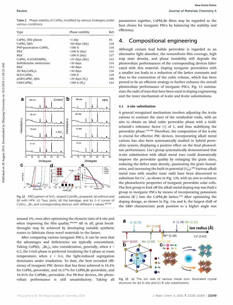
Table 2 Phase stability of CsPbI3 modified by various strategies undervarious conditions
Type Phase stability Ref.
CsPbI3 (HI) planar <1 day 85CsPbI3 QDs >60 days (dry) 128PVP-passivation CsPbI3 >500 h 138PEA+ >100 h (dry) 135PEA+ >200 h (dry) 137CsPbI3$0.025EDAPbI4 >35 days (dry) 132Sulfobetaine zwitterions >30 days 134PEA+ >40 days 1112D BA2CsPb2I7 >30 days 136SCG-CsPbI3 >500 h 139mGR/CsPbI3 QDs >30 days (N2) 180CHI/CsPbI3 >500 h (N2) 144
Fig. 12 XRD pattern of SnF2-doped CsSnIBr2 prepared: (a) without and(b) with HPA. (c) Tauc plots, (d) the bandgap, and (e) J–V curves ofCsSnI3�xBrx and corresponding devices with different x values.190,191
Fig. 13 (a) The ion radii of various metal ions. Illustrated crystal
Review Journal of Materials Chemistry A
Publ
ishe
d on
30
Aug
ust 2
019.
Dow
nloa
ded
by Z
hejia
ng U
nive
rsity
on
10/3
/201
9 11
:50:
33 A
M.
View Article Online
around 3%, even aer optimizing the element ratio of X site andwhen improving the lm quality.194,195 All in all, great break-throughs may be achieved by developing suitable syntheticroutes to fabricate these novel materials in the future.
Aer comparing various inorganic PSCs, it can be seen thatthe advantages and deciencies are typically concomitant.Taking CsPb(I1�xBrx)3 into consideration, generally, when x <0.2, the I-rich phase is preferred insulating the d phase at roomtemperature; when x > 0.4, the light-induced segregationdominates under irradiation. To date, the best recorded effi-ciency of inorganic PSC device that has been achieved is 18.4%for CsPbI3 perovskite, and 16.37% for CsPbI2Br perovskite, and10.91% for CsPbBr3 perovskite. For Pb-free devices, the photo-voltaic performance is still unsatisfactory. Taking all
This journal is © The Royal Society of Chemistry 2019
parameters together, CsPbI2Br lms may be regarded as thebest choice for inorganic PSCs by balancing the stability andefficiency.
4. Compositional engineering
Although cesium lead halide perovskite is regarded as analternative light absorber, the nonuniform lm coverage, hightrap state density, and phase instability still degrade thephotovoltaic performances of the corresponding devices fabri-cated with this material. Doping inorganic perovskites witha smaller ion leads to a reduction of the lattice constants andthus to the contraction of the cubic volume, which has beenproved to be an efficient strategy to further enhance the overallphotovoltaic performance of inorganic PSCs. Fig. 13 summa-rizes the radii of ions that have been used in doping engineeringand the inner mechanism of A-site and B-site substitutions.
4.1 A-site substitution
A general recognized mechanism involves adjusting the A-sitecations to contract the sizes of the octahedral voids, with anaim to obtain an ideal cubic perovskite phase with a Gold-schmidt's tolerance factor (s) of 1, and thus stabilizing theperovskite phase.114,196 Therefore, the composition of the A-siteis crucial for effective PSC devices. Incorporating alkali metalcations has also been systematically studied in hybrid perov-skite system, displaying a positive effect on the nal photovol-taic performance. Liu's group systematically demonstrated thatA-site substitution with alkali metal ions could dramaticallyimprove the perovskite quality by enlarging the grain sizes,reducing the defect state density, passivating the grain bound-aries, and increasing the built-in potential (Vbi).196 Various alkalimetal ions with smaller ionic radii have been discovered tosubstitute for Cs+, as shown in Fig. 13b, with an aim to enhancethe photoelectric properties of inorganic perovskite solar cells.The rst group to kick off the alkali metal doping way was Park'sgroup in inorganic PSCs by means of incorporating potassiumcations (K+) into the CsPbI2Br lattice.114 Aer optimizing thedoping dosage, as shown in Fig. 14a and b, the largest shi ofthe XRD characteristic peak position to a higher angle was
structure for (b) A-site and (c) B-site substitutions.
J. Mater. Chem. A, 2019, 7, 21036–21068 | 21049
Fig. 14 (a) XRD patterns and (b) Gaussian fitting curves for the (100)peaks of Cs1�xKxPbI2Br films (x ¼ 0, 0.025, 0.05, 0.075, 0.1). XPSspectra of CsPbI2Br (black) and Cs0.925K0.075PbI2Br (red) for (c) Cs 3d,(d) Pb 4f, (e) I 3d, and (f) Br 3d. (g) Absorbance spectra of Cs1�xKxPbI2Brfilms (x¼ 0, 0.025, 0.05, 0.075, 0.1). Time-resolved PL decay profiles of(h) CsPbI2Br and (i) Cs0.925K0.075PbI2Br films with and without a bl-TiO2
layer.114
Fig. 15 (a) XRD patterns for Cs1�xRxPbBr3 films. (b) XPS spectra of Cs3d for various alkali metal cations-doped perovskite films. (c) Enlargedcomparison of the (100), (110) and (111) diffraction peaks. Top-viewSEM images of the (d) CsPbBr3, (e) Cs0.98Li0.02PbBr3, (f) Cs0.94Na0.06-PbBr3, (g) Cs0.92K0.08PbBr3, and (h) Cs0.91Rb0.09PbBr3 films. (i) Grainstatistical distribution of five different films based on the top-viewimages.90
Journal of Materials Chemistry A Review
Publ
ishe
d on
30
Aug
ust 2
019.
Dow
nloa
ded
by Z
hejia
ng U
nive
rsity
on
10/3
/201
9 11
:50:
33 A
M.
View Article Online
observed upon a closer look for the (100) peak of Cs0.925K0.075-PbI2Br, which could be correlated with a signicant decrease inthe lattice constant from 6.0341 A to 6.0137 A, resulting in thecontraction of the cubic volume and a signicant stabilizationof the perovskite phase.197 Furthermore, the increased XRDpeak intensity indicated an increase in the crystallinity, wherebythe preferred orientation was arranged. The binding energy forPb 4f and Br 3d shied from 137.8 to 138.2 eV and 67.95 to68.35 eV owing to the changed interaction between theelements (see Fig. 14c–f) aer doping with K+, respectively.Arising from the smaller ion radius of potassium (1.38 A) thancesium (1.67 A), the volumetric ratio between PbX6 octahedraand A-site cations for Cs0.925K0.075PbI2Br could be well-tuned,leading to an enhancement of the phase stability of perov-skites. A signicant increase in absorbance intensity and theenhancement of charge extraction could also be viewed fromFig. 14g–i, which were highly dependent on the optimization ofthe as-prepared perovskite lm.
According to the passivation effect of potassium cations, thedefect state density could be signicantly reduced, such as thehalide vacancy in the grain boundaries or in the interior of theperovskite lm.198 The non-radiative losses could be dramati-cally eliminated owing to the suppressed recombination,thereby enhancing the external photoluminescence quantumyield as well as the corresponding photovoltaic conversionefficiency. Finally, a device with the architecture of FTO/bl-TiO2/Cs0.925K0.075PbI2Br/Spiro-OMeTAD/Au yielded an enhancedefficiency as high as 10.0%, demonstrating the feasibility toregulate the lattice and defect state density.
More recently, Tang's group comprehensively studieda series of alkali metal ions (Li+, Na+, K+, and Rb+) with smallerionic radii as dopants to modulate the lm quality of all-inorganic CsPbBr3 perovskite lms.90 As shown in Fig. 15, the
21050 | J. Mater. Chem. A, 2019, 7, 21036–21068
characteristic peaks shied to higher binding energy and thediffraction angle could also be discovered, conrming thecontraction in the perovskite cubic volume. By optimizing thedoping amount, the grain size could be enlarged to 820 nmfrom the pristine 360 nm size, as shown in Fig. 15d–i, leading tothe reduction of the grain boundaries, which would induceshallow states near the valence band edge and hinder holediffusion. In this fashion, the recombination in perovskite lmscould be suppressed.199 An unprecedented PCE of 9.86% andthe long-term stability of the HTL-free Cs0.91Rb0.09PbBr3 solarcell guarantee its further application.
4.2 B-site substitution
Can the partial substitution of Pb2+ (B-site) with other metalions (from an extent of doping to alloying) stabilize the desiredphase of CsPbX3 (X ¼ Cl, Br, I) perovskites without changingtheir optoelectronic properties? Considering the toxicity of Pb2+
in typical perovskite crystals, various bivalent nontoxic metalions (such as Mn2+, Zn2+, Cd2+, Co2+, Sr2+, Sn2+, and alkalineearth metal ions)70,113,116,126,197,200–202 and multi-valent nontoxicmetal (such as Bi3+, In3+, Y3+, Nb5+, and lanthanide rare earthions)97,129,203–207 have been introduced into the perovskite latticeto partially substitute Pb2+, realizing the optimization of thenally perovskite lms. According to previous reports, thereduction of the bond length between B2+ and X� can signi-cantly enhance the stability of CsPbX3 perovskites as well as thecorresponding performance of photovoltaic devices owing tothe optimized tolerance factor and enhanced formation energyfor a-CsPbI3 at room temperature and for the orthorhombicCsPbBr3, respectively, as shown in Fig. 16a.208 Zou et al. provedthat Pb2+ substitution with Mn2+ could result in latticecontraction and enhance the formation energy by means of
This journal is © The Royal Society of Chemistry 2019
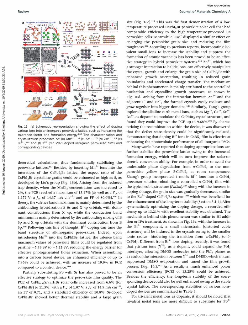
Fig. 16 (a) Schematic representation showing the effect of dopingvarious ions into an inorganic perovskite lattice, such as increasing thetolerance factor and formation energy.208 The characterization andcrystallization processes of: (b) Mn2+-,116 (c) Sr2+-,113 (d) Zn2+-,126 (e)Bi3+-,129 and (f) Y3+ (ref. 207)-doped inorganic perovskite films andcorresponding devices.
Review Journal of Materials Chemistry A
Publ
ishe
d on
30
Aug
ust 2
019.
Dow
nloa
ded
by Z
hejia
ng U
nive
rsity
on
10/3
/201
9 11
:50:
33 A
M.
View Article Online
theoretical calculations, thus fundamentally stabilizing theperovskite lattices.197 Besides, by inserting Mn2+ ions into theinterstices of the CsPbI2Br lattice, the aspect ratio of theCsPbI2Br crystalline grains could be enhanced as high as 8, asdeveloped by Liu's group (Fig. 16b). Arising from the reducedtrap density, when the MnCl2 concentration was increased to2%, the PCE reached a maximum of 13.47% (as well as a Voc of1.172 V, a Jsc of 14.37 mA cm�2, and an FF of 80.0%).116 Intheory, the valence band maximum is mainly determined by theantibonding hybridization B 6s and X np orbitals with domi-nant contributions from X np, while the conduction bandminimum is mainly determined by the antibonding mixing of B6p and X np orbitals with the dominant contribution from B6p.209 Following this line of thought, B2+ doping can tune theband structure of all-inorganic perovskites. Indeed, uponintroducing Mn2+ into the CsPbIBr2 lattice, the valence bandmaximum values of perovskite lms could be regulated frompristine �5.39 eV to �5.22 eV, reducing the energy barrier foreffective photogenerated holes extraction. When assemblinginto a carbon based device, an enhanced efficiency of up to7.36% could be achieved, with an increase of 19.9% in PCEcompared to a control device.200
Partially substituting Pb with Sr has also proved to be aneffective strategy to optimize the perovskite lm quality. ThePCE of CsPb0.98Sr0.02I2Br solar cells increased from 6.6% (forCsPbI2Br) to 11.3%, with a Voc of 1.07 V, a Jsc of 14.9 mA cm�2,an FF of 0.71, and a stabilized efficiency of 10.8%. Sr-dopedCsPbI2Br showed better thermal stability and a large grain
This journal is © The Royal Society of Chemistry 2019
size (Fig. 16c).113 This was the rst demonstration of a low-temperature-processed CsPbI2Br perovskite solar cell that hadcomparable efficiency to the high-temperature-processed Csperovskite cells. Meanwhile, Ca2+ displayed a similar effect onenlarging the perovskite grain size and reducing the lmroughness.202 According to previous reports, incorporating iso-valent small ions to increase the stability and suppress theformation of atomic vacancies has been proved to be an effec-tive strategy in hybrid perovskite systems.210 Zn2+, which hasa stronger interaction to halide ions, can effectively manipulatethe crystal growth and enlarge the grain size of CsPbI2Br withenhanced growth orientation, resulting in reduced grainboundaries and accelerated charge transfer. The mechanismbehind this phenomenon is mainly attributed to the controllednucleation and crystalline growth processes, as shown inFig. 16d. Arising from the interaction between Zn2+ and theadjacent I� and Br�, the formed crystals easily coalesce andgrow together into bigger domains.126 Similarly, Tang's groupexplored the alkaline earth metal ions, such as Mg2+, Ca2+, Sr2+,Ba2+, as dopants to modulate the CsPbBr3 crystal structure, andfound they could improve the PCE up to 9.68%.201 By charac-terizing the recombination within the device, it was discoveredthat the defect state density could be signicantly reduced,demonstrating that doping B2+ ions in CsBX3 lm is effective atenhancing the photovoltaic performance of all-inorganic PSCs.
Many works have reported that doping appropriate ions canfurther stabilize the perovskite lattice owing to the increasedformation energy, which will in turn improve the solar-to-electric conversion ability. For example, in order to avoid theundesirable phase degradation from a-CsPbI3 to the non-perovskite yellow phase d-CsPbI3 at room temperature,Zhang's group incorporated 4 mol% Bi3+ ions into a CsPbI3precursor solution, obtaining a controlled a-CsPbI3 lm withthe typical cubic structure (Pm3m).129 Along with the increase indoping dosage, the grain size was gradually decreased, similarto the Eu3+-doped CsPbI2Br system,205 which was benecial forthe enhancement of the long-term stability (Section 3.1.4). Aersystematically optimizing the doping dosage, a recorded effi-ciency up to 13.21% with excellent stability was obtained. Themechanism behind this phenomenon was similar to HI addi-tion or IPA treatment. As shown in Fig. 16e, with the increase inthe Bi3+ component, a small microstrain (distorted cubicstructure) will be induced in the crystals owing to the smallerionic radius, hindering the transition from a-CsPbI3 to d-CsPbI3. Different from Bi3+ ions doping, recently, it was foundthat yttrium ions (Y3+), as a dopant, could expand the PbI2interlayer, allowing DMOS molecules into the PbI2 planes asa result of the interaction between Y3+ and DMSO, which in turnsuppressed DMSO evaporation and tuned the lm growthprocess (Fig. 16f).207 As a result, a much enhanced powerconversion efficiency (PCE) of 13.25% could be achieved.Besides the efficiency, the long-term stability of the corre-sponding device could also be well enhanced owing to the stablecrystal lattice. The corresponding stabilities of various ions-doped devices are summarized in Table 3.
For trivalent metal ions as dopants, it should be noted thattrivalent metal ions are more difficult to substitute for Pb2+
J. Mater. Chem. A, 2019, 7, 21036–21068 | 21051
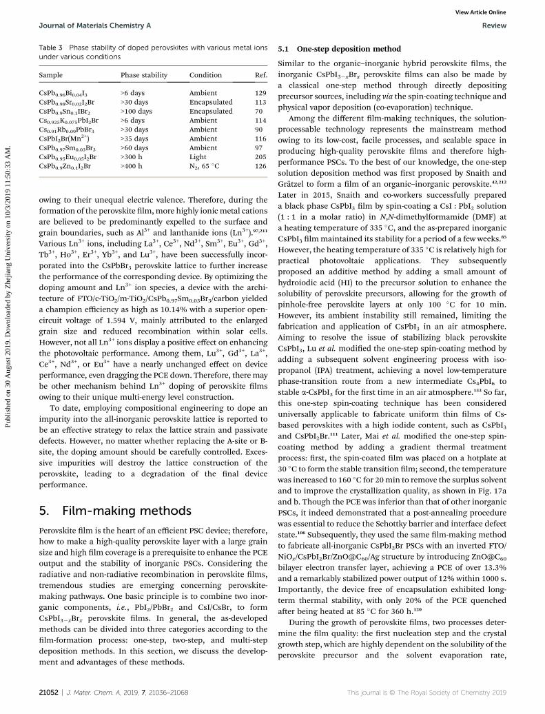
Table 3 Phase stability of doped perovskites with various metal ionsunder various conditions
Sample Phase stability Condition Ref.
CsPb0.96Bi0.04I3 >6 days Ambient 129CsPb0.98Sr0.02I2Br >30 days Encapsulated 113CsPb0.9Sn0.1IBr2 >100 days Encapsulated 70Cs0.925K0.075PbI2Br >6 days Ambient 114Cs0.91Rb0.09PbBr3 >30 days Ambient 90CsPbI2Br(Mn2+) >35 days Ambient 116CsPb0.97Sm0.03Br3 >60 days Ambient 97CsPb0.95Eu0.05I2Br >300 h Light 205CsPb0.9Zn0.1I2Br >400 h N2, 65 �C 126
Journal of Materials Chemistry A Review
Publ
ishe
d on
30
Aug
ust 2
019.
Dow
nloa
ded
by Z
hejia
ng U
nive
rsity
on
10/3
/201
9 11
:50:
33 A
M.
View Article Online
owing to their unequal electric valence. Therefore, during theformation of the perovskite lm,more highly ionic metal cationsare believed to be predominantly expelled to the surface andgrain boundaries, such as Al3+ and lanthanide ions (Ln3+).97,211
Various Ln3+ ions, including La3+, Ce3+, Nd3+, Sm3+, Eu3+, Gd3+,Tb3+, Ho3+, Er3+, Yb3+, and Lu3+, have been successfully incor-porated into the CsPbBr3 perovskite lattice to further increasethe performance of the corresponding device. By optimizing thedoping amount and Ln3+ ion species, a device with the archi-tecture of FTO/c-TiO2/m-TiO2/CsPb0.97Sm0.03Br3/carbon yieldeda champion efficiency as high as 10.14% with a superior open-circuit voltage of 1.594 V, mainly attributed to the enlargedgrain size and reduced recombination within solar cells.However, not all Ln3+ ions display a positive effect on enhancingthe photovoltaic performance. Among them, Lu3+, Gd3+, La3+,Ce3+, Nd3+, or Eu3+ have a nearly unchanged effect on deviceperformance, even dragging the PCE down. Therefore, theremaybe other mechanism behind Ln3+ doping of perovskite lmsowing to their unique multi-energy level construction.
To date, employing compositional engineering to dope animpurity into the all-inorganic perovskite lattice is reported tobe an effective strategy to relax the lattice strain and passivatedefects. However, no matter whether replacing the A-site or B-site, the doping amount should be carefully controlled. Exces-sive impurities will destroy the lattice construction of theperovskite, leading to a degradation of the nal deviceperformance.
5. Film-making methods
Perovskite lm is the heart of an efficient PSC device; therefore,how to make a high-quality perovskite layer with a large grainsize and high lm coverage is a prerequisite to enhance the PCEoutput and the stability of inorganic PSCs. Considering theradiative and non-radiative recombination in perovskite lms,tremendous studies are emerging concerning perovskite-making pathways. One basic principle is to combine two inor-ganic components, i.e., PbI2/PbBr2 and CsI/CsBr, to formCsPbI3�xBrx perovskite lms. In general, the as-developedmethods can be divided into three categories according to thelm-formation process: one-step, two-step, and multi-stepdeposition methods. In this section, we discuss the develop-ment and advantages of these methods.
21052 | J. Mater. Chem. A, 2019, 7, 21036–21068
5.1 One-step deposition method
Similar to the organic–inorganic hybrid perovskite lms, theinorganic CsPbI3�xBrx perovskite lms can also be made bya classical one-step method through directly depositingprecursor sources, including via the spin-coating technique andphysical vapor deposition (co-evaporation) technique.
Among the different lm-making techniques, the solution-processable technology represents the mainstream methodowing to its low-cost, facile processes, and scalable space inproducing high-quality perovskite lms and therefore high-performance PSCs. To the best of our knowledge, the one-stepsolution deposition method was rst proposed by Snaith andGratzel to form a lm of an organic–inorganic perovskite.42,212
Later in 2015, Snaith and co-workers successfully prepareda black phase CsPbI3 lm by spin-coating a CsI : PbI2 solution(1 : 1 in a molar ratio) in N,N-dimethylformamide (DMF) ata heating temperature of 335 �C, and the as-prepared inorganicCsPbI3 lmmaintained its stability for a period of a few weeks.85
However, the heating temperature of 335 �C is relatively high forpractical photovoltaic applications. They subsequentlyproposed an additive method by adding a small amount ofhydroiodic acid (HI) to the precursor solution to enhance thesolubility of perovskite precursors, allowing for the growth ofpinhole-free perovskite layers at only 100 �C for 10 min.However, its ambient instability still remained, limiting thefabrication and application of CsPbI3 in an air atmosphere.Aiming to resolve the issue of stabilizing black perovskiteCsPbI3, Lu et al. modied the one-step spin-coating method byadding a subsequent solvent engineering process with iso-propanol (IPA) treatment, achieving a novel low-temperaturephase-transition route from a new intermediate Cs4PbI6 tostable a-CsPbI3 for the rst time in an air atmosphere.133 So far,this one-step spin-coating technique has been considereduniversally applicable to fabricate uniform thin lms of Cs-based perovskites with a high iodide content, such as CsPbI3and CsPbI2Br.111 Later, Mai et al. modied the one-step spin-coating method by adding a gradient thermal treatmentprocess: rst, the spin-coated lm was placed on a hotplate at30 �C to form the stable transition lm; second, the temperaturewas increased to 160 �C for 20min to remove the surplus solventand to improve the crystallization quality, as shown in Fig. 17aand b. Though the PCE was inferior than that of other inorganicPSCs, it indeed demonstrated that a post-annealing procedurewas essential to reduce the Schottky barrier and interface defectstate.106 Subsequently, they used the same lm-making methodto fabricate all-inorganic CsPbI2Br PSCs with an inverted FTO/NiOx/CsPbI2Br/ZnO@C60/Ag structure by introducing ZnO@C60
bilayer electron transfer layer, achieving a PCE of over 13.3%and a remarkably stabilized power output of 12% within 1000 s.Importantly, the device free of encapsulation exhibited long-term thermal stability, with only 20% of the PCE quenchedaer being heated at 85 �C for 360 h.120
During the growth of perovskite lms, two processes deter-mine the lm quality: the rst nucleation step and the crystalgrowth step, which are highly dependent on the solubility of theperovskite precursor and the solvent evaporation rate,
This journal is © The Royal Society of Chemistry 2019

Fig. 17 (a) Schematic view of the gradient thermal treatment process,and (b) XRD spectra of as-prepared perovskite films fabricated withdifferent methods. (c) Illustration of the gradient thermal annealingprocesses with anti-solvent treatment by Tol and IPA. (d) Schematic ofSCG technology.106,124,139
Review Journal of Materials Chemistry A
Publ
ishe
d on
30
Aug
ust 2
019.
Dow
nloa
ded
by Z
hejia
ng U
nive
rsity
on
10/3
/201
9 11
:50:
33 A
M.
View Article Online
respectively. Following this line of thought, the precursorsolution temperature is another crucial parameter for sup-pressing the formation of too many nuclei and for increasingthe crystallization rate. Liu's group systematically studied therelationship between crystallization and the fabricationtemperature, and found that a precursor solution temperaturexed at 100 �C could dramatically enlarge the grain size ofa CsPbI2Br lm.213 When assembling into a planar architecturedevice, a maximum PCE of up to 14.81% was achieved,demonstrating the importance of temperature in one-step spin-coating technology.
According to the above-mentioned discussion, precisecontrol of the crystal growth plays a crucial role in obtaininghigh-quality perovskite lms. Therefore, gradient thermalannealing (GTA) was further developed by Chen et al., in whichthe phase conversion was conducted under 50 �C for 1 min,100 �C for 1 min, and then 160 �C for 10 min, as shown inFig. 17c.124 When further processing the lm with anti-solvent(ATS) treatment, such as toluene (Tol) and isopropanol (IPA),
This journal is © The Royal Society of Chemistry 2019
a high-quality CsPbI2Br lm with increased average grain sizesand reduced defect density could be obtained, which wasmainly attributed to the rapid extraction of the residual solventby isopropanol. Finally, a record efficiency of up to 16.07% wasachieved. Strikingly, You's group further improved the one-stepspin-coating method with an intermediate solvent-controlledgrowth, called SCG, to obtain CsPbI3-perovskite lms free ofpinholes and a crystal size above 5 mm.139 SCG, in detail, refersto the process whereby the precursor lms were stored ina nitrogen glove box for several tens of minutes before anneal-ing on a hotplate (Fig. 17d). This stagnation allowed theresidual DMSO to improve the lm quality by enhancing themass transport and diffusion, achieving the champion PCE(15.7%) of CsPbI3 perovskite solar cells; further, there was nochange in the XRD patterns or absorption spectra aer 7 days ofstorage.
In summary, there are dozens of reports about depositinghigh-quality perovskite lms with a large grain size by a one-step method. The growth of perovskite lm follows the“Volmer–Weber” growth mode, accompanied with a classic“heterogeneous” nucleation process and grain growth theory. Indetail, the number of grains per unit area (Z) is determined bythe nucleation formation rate (vn) and the crystal growth rate(vc), following the formula: Z f (vn/vc), where Z is inverselyproportional to the grain size. Therefore, retarding the nucle-ation process and accelerating the grain growth process are twostrategies to increase the lm quality. To date, the one-stepmethod has been applicable to most cesium perovskites, suchas CsPbI3, CsPbI2Br, and even CsPbIBr2, but not for CsPbBr3,owing to its inferior solubility.
Although the solution-processable method provides greatadvantages to establish an ideal perovskite lm, the environ-mental conditions during perovskite lm formation, such astemperature, precursor solubility, atmosphere, annealing time,and so on, lead to an inferior repeatability. In order to overcomethese issues, the physical co-evaporation technique was furtherattempted to obtain an inorganic perovskite light-harvestinglayer by Ho-Baillie et al.104 As is well known, a dual sourcethermal evaporation technique was rst employed in a hybridperovskite system.214 In detail, an equal molar of CsX and PbX2
were simultaneously evaporated onto an FTO glass substratesupported electrode, leading to the successful crystallization ofa CsPbX3 perovskite lm. This physical process did not involveany solvents, therefore, there was no solvent residue le in thelm and so this technology is applicable to deposit insolublematerials. Troshin and co-workers prepared CsPbI3 lms bythermally co-evaporating CsI and PbI2 precursors undera vacuum environment for planar heterojunction inorganicPSCs (Fig. 18a).130 Different from spin-coated lms, the low-temperature brown perovskite phase of CsPbI3 is a particularfeature for vacuum thermal co-evaporation processes, as it isunstable and undergoes an irreversible transformation toa yellow phase under heating at temperatures above 60 �C. Onthe contrary, when heated up to 320 �C, the yellow phaseundergoes a phase transition back to the black phase, which isdepicted in Fig. 18b. Film annealing at 320 �C offers the bestoptimal light absorbance, which is consistent with the phase
J. Mater. Chem. A, 2019, 7, 21036–21068 | 21053
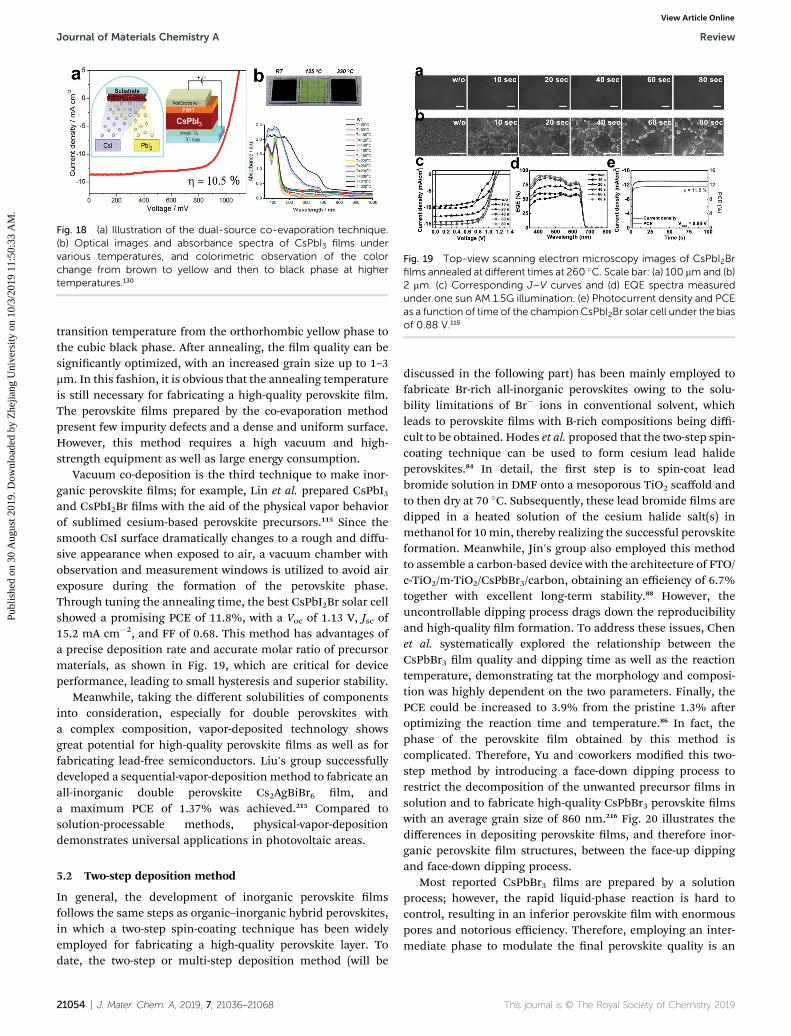
Fig. 18 (a) Illustration of the dual-source co-evaporation technique.(b) Optical images and absorbance spectra of CsPbI3 films undervarious temperatures, and colorimetric observation of the colorchange from brown to yellow and then to black phase at highertemperatures.130
Fig. 19 Top-view scanning electron microscopy images of CsPbI2Brfilms annealed at different times at 260 �C. Scale bar: (a) 100 mmand (b)2 mm. (c) Corresponding J–V curves and (d) EQE spectra measuredunder one sun AM 1.5G illumination. (e) Photocurrent density and PCEas a function of time of the champion CsPbI2Br solar cell under the biasof 0.88 V.115
Journal of Materials Chemistry A Review
Publ
ishe
d on
30
Aug
ust 2
019.
Dow
nloa
ded
by Z
hejia
ng U
nive
rsity
on
10/3
/201
9 11
:50:
33 A
M.
View Article Online
transition temperature from the orthorhombic yellow phase tothe cubic black phase. Aer annealing, the lm quality can besignicantly optimized, with an increased grain size up to 1–3mm. In this fashion, it is obvious that the annealing temperatureis still necessary for fabricating a high-quality perovskite lm.The perovskite lms prepared by the co-evaporation methodpresent few impurity defects and a dense and uniform surface.However, this method requires a high vacuum and high-strength equipment as well as large energy consumption.
Vacuum co-deposition is the third technique to make inor-ganic perovskite lms; for example, Lin et al. prepared CsPbI3and CsPbI2Br lms with the aid of the physical vapor behaviorof sublimed cesium-based perovskite precursors.115 Since thesmooth CsI surface dramatically changes to a rough and diffu-sive appearance when exposed to air, a vacuum chamber withobservation and measurement windows is utilized to avoid airexposure during the formation of the perovskite phase.Through tuning the annealing time, the best CsPbI2Br solar cellshowed a promising PCE of 11.8%, with a Voc of 1.13 V, Jsc of15.2 mA cm�2, and FF of 0.68. This method has advantages ofa precise deposition rate and accurate molar ratio of precursormaterials, as shown in Fig. 19, which are critical for deviceperformance, leading to small hysteresis and superior stability.
Meanwhile, taking the different solubilities of componentsinto consideration, especially for double perovskites witha complex composition, vapor-deposited technology showsgreat potential for high-quality perovskite lms as well as forfabricating lead-free semiconductors. Liu's group successfullydeveloped a sequential-vapor-deposition method to fabricate anall-inorganic double perovskite Cs2AgBiBr6 lm, anda maximum PCE of 1.37% was achieved.215 Compared tosolution-processable methods, physical-vapor-depositiondemonstrates universal applications in photovoltaic areas.
5.2 Two-step deposition method
In general, the development of inorganic perovskite lmsfollows the same steps as organic–inorganic hybrid perovskites,in which a two-step spin-coating technique has been widelyemployed for fabricating a high-quality perovskite layer. Todate, the two-step or multi-step deposition method (will be
21054 | J. Mater. Chem. A, 2019, 7, 21036–21068
discussed in the following part) has been mainly employed tofabricate Br-rich all-inorganic perovskites owing to the solu-bility limitations of Br� ions in conventional solvent, whichleads to perovskite lms with B-rich compositions being diffi-cult to be obtained. Hodes et al. proposed that the two-step spin-coating technique can be used to form cesium lead halideperovskites.84 In detail, the rst step is to spin-coat leadbromide solution in DMF onto a mesoporous TiO2 scaffold andto then dry at 70 �C. Subsequently, these lead bromide lms aredipped in a heated solution of the cesium halide salt(s) inmethanol for 10min, thereby realizing the successful perovskiteformation. Meanwhile, Jin's group also employed this methodto assemble a carbon-based device with the architecture of FTO/c-TiO2/m-TiO2/CsPbBr3/carbon, obtaining an efficiency of 6.7%together with excellent long-term stability.88 However, theuncontrollable dipping process drags down the reproducibilityand high-quality lm formation. To address these issues, Chenet al. systematically explored the relationship between theCsPbBr3 lm quality and dipping time as well as the reactiontemperature, demonstrating tat the morphology and composi-tion was highly dependent on the two parameters. Finally, thePCE could be increased to 3.9% from the pristine 1.3% aeroptimizing the reaction time and temperature.86 In fact, thephase of the perovskite lm obtained by this method iscomplicated. Therefore, Yu and coworkers modied this two-step method by introducing a face-down dipping process torestrict the decomposition of the unwanted precursor lms insolution and to fabricate high-quality CsPbBr3 perovskite lmswith an average grain size of 860 nm.216 Fig. 20 illustrates thedifferences in depositing perovskite lms, and therefore inor-ganic perovskite lm structures, between the face-up dippingand face-down dipping process.
Most reported CsPbBr3 lms are prepared by a solutionprocess; however, the rapid liquid-phase reaction is hard tocontrol, resulting in an inferior perovskite lm with enormouspores and notorious efficiency. Therefore, employing an inter-mediate phase to modulate the nal perovskite quality is an
This journal is © The Royal Society of Chemistry 2019

Fig. 20 (a) Fabrication processes for CsPbBr3 films by a dippingprocess and face-down dipping methods. (b) Mechanisms of thedipping reaction by a face-up dipping and face-down dippingprocess.216
Fig. 21 (a) Extraction of Br2 vapor from a bottle of bromine solution;Br2-vapor-assisted CVD process and reaction process; (b) solar cellarchitecture and J–V curve obtained in a reverse scan.87 (c) Illustrationof the spray-assisted deposition of CsPbIBr2 perovskite film and (d)–(e)XRD spectra of CsPbIBr2 perovskite films prepared under differentconditions.105
Review Journal of Materials Chemistry A
Publ
ishe
d on
30
Aug
ust 2
019.
Dow
nloa
ded
by Z
hejia
ng U
nive
rsity
on
10/3
/201
9 11
:50:
33 A
M.
View Article Online
effective strategy. Inspired by the rapid reaction betweenMAPbI3 and gaseous Br2 and HBr,146 Sun et al. fabricateda CsPbBr3 perovskite lm with a Br2-vapor-assisted CVDmethod, as shown in Fig. 21a, in which fast anion exchangefrom CsPbI3 to CsPbBr3 could be realized owing to the effectiveincorporation of Br� into CsPbI3 inorganic perovskites in a fewof seconds.87 First, the CsPbI3 precursors were spin-coated ontothe FTO/c-TiO2/m-TiO2 substrates, and then transferred intoa quartz tube furnace. Aer pumping the quartz tube for 5 min,the CsPbI3 precursors were heated to 150 �C and then Br2 vaporwas injected into the hot quartz tube for reaction. Finally, theperovskite lms were taken out and rinsed with isopropanol,and annealed in ambient air to obtain a bright yellow CsPbBr3layer. Finally, a relatively high PCE of up to 5.38% (Fig. 21b) wasachieved based on this CsPbBr3 all-inorganic perovskite solarcell with carbon as the back electrode. The perovskite layermade by the vapor-assisted method always features highcoverage, a smooth surface, and tiny grain size, thus reducingthe surface recombination rate during carrier transportationand thereby achieving a high Voc output. Moreover, the vapor-
This journal is © The Royal Society of Chemistry 2019
assisted technique does not need special requirements, it iseconomical and environmental compared to the co-evaporationor solution-processable spin-coating methods.
Perovskite-structured quantum dots (QDs) have also beenapplied to assemble perovskite lms for photovoltaic applica-tions, and are benecial for eliminating the inconclusive self-assembly crystallization processes as determined by differentfactors including the precursor ratio, solvent, processing addi-tives, substrate roughness and surface energy, atmospheric/environmental conditions, annealing temperature, and treat-ment time. To the best of our knowledge, CsPbI3 QDs haverecently been utilized to stabilize the crystal phase for the rsttime, which was discussed in Section 3.1.4.128 By spin-coatingQDs onto the surface of TiO2 lm, a high Voc of 1.23 V andefficiency of 10.77% were obtained, demonstrating the greatpotential for enhancing the overall photovoltaic performance ofall-inorganic PSCs. Subsequently, a CsPbBr3 QDs “ink” wasdeveloped to fabricate fully air-processed and stable solar cells,exhibiting an efficiency over 5% with high Voc values.157,217,218
This strategy may provide a new path to resolve the dissolutionissue of the CsPbBr3 precursor.
The uniform deposition and reliable anchoring of perovskiteprecursors in larger sizes oen requires specic conditions, butspray-assisted deposition is regarded as a straightforward, fast,and cost-effective way to pattern substrates on a large scale. Ho-Baillie et al. demonstrated the feasibility of spray-assisted
J. Mater. Chem. A, 2019, 7, 21036–21068 | 21055

Journal of Materials Chemistry A Review
Publ
ishe
d on
30
Aug
ust 2
019.
Dow
nloa
ded
by Z
hejia
ng U
nive
rsity
on
10/3
/201
9 11
:50:
33 A
M.
View Article Online
deposition to overcome the poor solubility of the bromide ion inone-step and two-step solution methods.105 In this method, CsIwas sprayed onto a spin-coated PbBr2 layer under ambientconditions (see Fig. 21c). The substrate temperature during thespraying of CsI and the annealing temperature were found to bethe most crucial parameters for the quality of the perovskitelm. As depicted in Fig. 21d, the main peaks at 14.82�, 21.05�,and 29.94� corresponding to the (100), (110), and (220) planes ofthe CsPbIBr2 perovskite orthorhombic phase could be clearlydetected. With a much higher substrate temperature, thesegregation of CsI (27.5�) became prominent. Fig. 21e demon-strates the crystallization of CsPbIBr2 perovskite aer annealingat 275 �C, 300 �C, 325 �C, or 350 �C for 10 min in atmosphericconditions, suggesting that a good annealing temperaturerange is from 275 �C to 350 �C. Using the optimized spray-assisted method, the best-performing inorganic FTO/bl-TiO2/mp-TiO2/CsPbIBr2/Spiro-OMeTAD/Au PSC achieved a stabilizedPCE of 6.3% with negligible hysteresis.
Fig. 22 (a) The steps of depositing c-TiO2, m-TiO2, and PbBr2. (b)Multi-step solution-processed deposition of CsBr. (c) Top-view and (d)cross-sectional SEM images of the all-inorganic lead halide film. (e)Crystal structure of the cesium lead bromide halide.89
5.3 Multi-step deposition method
To date, the multi-step technology is generally employed tofabricate all-brominated CsPbBr3 perovskite lms. During thefabrication process of CsPbBr3 perovskite lms, CsPb2Br5 orCs4PbBr6 will be formed when employing the traditional two-step solution-processed lm-making technique. To effectivelyresolve this issue, a novel multi-step method to form a high-purity cesium lead bromide lm with vertical and monolayer-aligned largest grains were proposed by Tang's group, leadingto maximizing the charge transportation kinetics and thereforean increased PCE from 6.7% to 9.72% aer incorporatingGQDs.89
A schematic diagram of multi-step deposition technology isshown in Fig. 22a–d, involving a single PbBr2 layer and themulti-step spin-coating of a CsBr layer. By tuning the number ofdeposition cycles with the CsBr solution, the components,crystal structure, and morphological alignment of the as-prepared perovskite lms could be well controlled. From theSEM images, it could be seen that the lm coverage and grainsize were insufficient when the deposition number was low.Along with increasing the deposition number, an ideal perov-skite lm could be obtained when the deposition number wascontrolled at 4 times. Themechanism behind this phenomenoncan be explained by the gradual phase conversion and crystalgrowth processes. Through characterizing the phases of as-prepared perovskite lms with various deposition numbers ofCsBr solution, the crystalline phase conversion during themulti-step process can be summarized into three reactions asfollows:
2PbBr2 + CsBr / CsPb2Br5 (n # 3) (1)
CsPb2Br5 + CsBr / 2CsPbBr3 (n ¼ 4) (2)
CsPbBr3 + 3CsBr / Cs4PbBr6 (n $ 5) (3)
21056 | J. Mater. Chem. A, 2019, 7, 21036–21068
In this fashion, fewer CsBr coating cycles generally lead tothe formation of a PbBr2-rich CsPb2Br5-dominant lm, whilea higher number of CsBr coating cycles will accelerate thereaction of the CsPbBr3 phase with CsBr to form a CsBr-richCs4PbBr6-dominant lm. Therefore, by a precise control of theamount of CsBr, a high-purity inorganic perovskite lm witha minimized mixed phase can be obtained. The thin lm withvertical and monolayer-aligned grains has a lower density ofdefect states and fewer grain boundaries, and therefore theabsorption layer is expected to further improve the deviceperformance upon assembly into a photovoltaic device.
Similarly, spray-coating technology has been widely used inindustrial processes due to its advantages in scaling up for largearea cella.219,220 Inspired by the above-mentioned conclusion,a multi-step spraying method was further developed to fabricatelarge-area solar cell devices by Tang's group.98 Their studiesrevealed an identical phase conversion from PbBr2-rich CsPb2-Br5 to perovskite-structured CsPbBr3 and further to CsBr-richCs4PbBr6 by spraying CsBr multilayers sequentially, which wasin accordance with a previous report.89 Following the above-mentioned discussion, an evaporation-assisted solutionmethod was further developed, as shown in Fig. 23a. Based ontheir conclusion, the corresponding phase conversion fromCsPb2Br5 to CsPbBr3 and then to Cs4PbBr6 was also conrmed.By optimizing the CsBr deposition time and accelerating thecharge transfer, a high efficiency of up to 10.45% was ob-tained.102 Obtaining a high-purity CsPbBr3 lm provides a newavenue for making high-performance inorganic PSCs by multi-step spray-assisted method besides the commonly used one-step and two-step techniques, which require a high-temperature annealing process.
This journal is © The Royal Society of Chemistry 2019
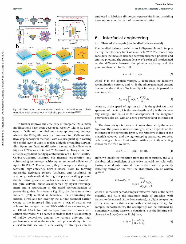
Fig. 23 Illustration on evaporation-assisted deposition and phasetransition induced methods of CsPbBr3 perovskite film.102,103
Review Journal of Materials Chemistry A
Publ
ishe
d on
30
Aug
ust 2
019.
Dow
nloa
ded
by Z
hejia
ng U
nive
rsity
on
10/3
/201
9 11
:50:
33 A
M.
View Article Online
To further improve the efficiency of inorganic PSCs, manymodications have been developed recently. Liu et al. devel-oped a facile and modied multistep spin-coating strategy,wherein the PbBr2 lm was rst immersed into CsBr solution(two-step deposition method), with a subsequent spin-coatingof a multi-layer of CsBr to realize a highly crystalline CsPbBr3lm. Upon interfacial modication, a remarkable efficiency ashigh as 8.79% was obtained.221 Meanwhile, Tong et al. con-structed a gradient bandgap architecture of CsPbBr3/CsPbBr3–CsPb2Br5/CsPbBr3–Cs4PbBr6 via thermal evaporation andspin-coating technology, achieving an enhanced efficiency ofup to 10.17%.101 Furthermore, they developed a strategy tofabricate high-efficiency CsPbBr3-based PSCs by formingperovskite derivative phases (CsPb2Br5 and Cs4PbBr6) viaa vapor growth method. During the post-annealing process,the derivative phases as nucleation sites are transformed tothe pure CsPbBr3 phase accompanied by crystal rearrange-ment and a retardation in the rapid recrystallization ofperovskite grains. As shown in Fig. 23b, the phase transition-induced (PTI) method is benecial for eliminating theinternal stress and for lowering the surface potential barrier.Owing to the improved lm quality, a PCE of 10.91% wasachieved for n–i–p structured PSCs with silver electrodes, anda PCE of 9.86% for hole-transport-layer-free devices withcarbon electrodes.103 To date, it is obvious that a key advantageof halide perovskites among the various different high-performance semiconductors is their processability. As dis-cussed in this section, a wide variety of strategies can be
This journal is © The Royal Society of Chemistry 2019
employed to fabricate all-inorganic perovskite lms, providingmore options on the path of commercialization.
6. Interfacial engineering6.1 Theoretical analysis (the detailed balance model)
The detailed balance model is an indispensable tool for pre-dicting the efficiency limit of solar cells.222,223 The model onlyconsiders the detailed balance between absorbed photons andemitted photons. The current density of a solar cell is calculatedas the difference between the photons radiating and thephotons absorbed by the cell:
J ¼ Je(V) � Jph (2)
where V is the applied voltage, Je represents the radiativerecombination current, and Jph is the photogenerated currentdue to the absorption of incident light in inorganic perovskitematerials, i.e.,
Jph ¼ q
ðN0
aðl;LÞGðlÞlhc0
dl (3)
where c0 is the speed of light in air, G is the global AM 1.5Gspectrum of the Sun, l is the wavelength, and q is the elemen-tary charge, and a(l,L) is the absorptivity of the inorganicperovskite solar cell with an active perovskite layer thickness ofL.
The absorptivity a is the ratio of power absorbed by the activelayer over the power of incident sunlight, which depends on thethickness of the perovskite layer L, the refractive indices of thematerials adopted, and the light-trapping structures. For solarcells having a planar front surface with a perfectly reectingmirror on the rear, we have:
a(l,L) ¼ 1 � exp[�2a(l)L] (4)
Here, we ignore the reection from the front surface, and a isthe absorption coefficient of the active material. For solar cellshaving a randomly textured front surface with a perfectlyreecting mirror on the rear, the absorptivity can be writtenas:224,225
aðl;L; qmÞ ¼ aðlÞ
aðlÞ þ sin2qmðlÞ
4ðnrðlÞÞ2L
(5)
where nr is the real part of complex refractive index of the activematerial, and qm is the maximum angle of emission (withrespect to the normal of the front surface), i.e., light escapes outof the solar cell within a cone with a solid angle of qm. Forcomplex nanostructures, the absorptivity can be obtained bynumerically solving Maxwell's equations. For the limiting effi-ciency (Shockley–Queisser limit) case,
aðlÞ ¼�1; l# lg0; l. lg
(6)
J. Mater. Chem. A, 2019, 7, 21036–21068 | 21057

Journal of Materials Chemistry A Review
Publ
ishe
d on
30
Aug
ust 2
019.
Dow
nloa
ded
by Z
hejia
ng U
nive
rsity
on
10/3
/201
9 11
:50:
33 A
M.
View Article Online
where lg is the bandgap wavelength of the inorganic perovskitematerial. An ideal cell will absorb all the photons with energyabove the bandgap energy.
According to the detailed balance theory and Boltzmannstatistics, the radiative recombination current Je can beexpressed as:
Je ¼ J0e
�exp
�qV
kBT
�� 1
�(7)
where J0e is the radiative saturation current, which is theminimum of the (reverse) saturation current. J0e can be calcu-lated by the blackbody radiation law:
J0e ¼ q
ðN0
aðl;LÞG0ðl;TÞlhc0
dl
G0ðl;TÞ ¼ð2p0
d4
ðqmðlÞ0
Sðl;TÞcosðqÞsinðqÞdq
¼ p sin2qmðlÞSðl;TÞ Sðl;TÞ ¼ 2hc0
2
l51
exp� hc0
lkBT
�� 1
(8)
where G0(l,T) is the blackbody emission spectrum of the solarcell operated at the temperate T, and S(l,T) is the correspondingthermal radiance of the cell.
For a solar cell system, the dominated thermodynamic loss iscaused by the non-radiative recombination, including theShockley–Read–Hall (SRH) recombination (monomolecularrecombination) and Auger recombination. The defects, impu-rities or deep-level traps at the bulk and interface will induce theSRH recombination, while the high carrier density by injectionor generation will induce the Auger recombination, whichalways occurs in heavily doped inorganic semiconductors.Consequently, to describe the electrical response of a practicalinorganic perovskite solar cell, the non-radiative recombinationcurrent should be introduced. Thus, eqn (2) should be modiedas:
J ¼ Jn;srhðVÞ þ Jn;augðVÞ þ JeðVÞ � Jph
Jn;srhðVÞ ¼ J0n;srh
�exp
�qV
2kBT
�� 1
�; J0n;srh ¼ qCsrhLni
Jn;augðVÞ ¼ J0n;aug
�exp
�3qV
2kBT
�� 1
�; J0n;aug ¼ qCaugLni
3
(9)
where Jn,srh and Jn,aug are the non-radiative recombinationcurrents for the SRH and Auger recombination, respectively,Csrh and Caug are the SRH and Auger recombination rates,respectively, and J0n,srh and J0n,aug are the non-radiative satu-ration currents for the SRH and Auger recombination,respectively.
One may approximate eqn (9) as a more compact form givenby:
Jz JðVÞ � Jph
JðVÞ ¼ J0
�exp
�qV
mkBT
�� 1
� (10)
where J is the total recombination current including the radia-tive and nonradiative ones and m is the ideality factor, and J0 is
21058 | J. Mater. Chem. A, 2019, 7, 21036–21068
the dark current or saturation current, which should be thesuperposition of the radiative saturation current J0e and thenon-radiative saturation currents J0n,srh and J0n,aug. From eqn(10), we can obtain the expression of Voc for the inorganicperovskite solar cells:
Voc ¼ mkBT
qlog
�Jph
J0
�(11)
Thus, we can extract the ideality factor m to understand therecombination mechanism of the inorganic perovskite solarcells by investigating the light-intensity-dependent Voc curve.Fig. 24 shows the Voc–log(Jph) curve for a CsPbBr3 system, andmis approximate to 2. Therefore, the dominant recombination ininorganic PSCs is the SRH recombination.
Also, we can split the saturation current into radiative andnon-radiative ones, i.e.,
J0 ¼ J0e þ J0n;srh þ J0n;aug ¼ J0e þ J0n ¼ J0ehELQE
hELQE ¼ J0e
J0e þ J0n
(12)
where hELQE is the external luminescence quantum efficiency(ELQE).226 The ELQE is the number of photons emitted intofree space over the number of electron–hole pairs generated bylight absorption, which is a gure of merit for the photonrecycling of inorganic perovskite solar cells.227 Finally, weconsider two circuit quantities involving the series resistanceRs, describing the ohmic loss from the interfaces and elec-trodes, and the shunt resistance Rsh, describing the shuntcurrent resulting from the voids and defects. The two circuitparameters are essential to the ll factor of the inorganicperovskite solar cells. Incorporating the series and shuntresistances into the detailed balance model, the modiedmodel can be written as:228
J ¼ V � JRs
Rsh
þ Jn;srhðV � JRsÞ þ Jn;augðV � JRsÞ
þJeðV � JRsÞ � Jph (13)
Fig. 24 The Voc–log(Jph) curve for an all-inorganic CsPbBr3 PSC.
This journal is © The Royal Society of Chemistry 2019

Review Journal of Materials Chemistry A
Publ
ishe
d on
30
Aug
ust 2
019.
Dow
nloa
ded
by Z
hejia
ng U
nive
rsity
on
10/3
/201
9 11
:50:
33 A
M.
View Article Online
here, eqn (13) is the modied detailed balance model to capturethe current density–voltage characteristics of the inorganicperovskite solar cells.
From the detailed balance theory and eqn (2), it is easy topredict the limiting efficiency of inorganic PSCs. Table 4 liststhe calculated results for the commonly-used inorganic perov-skite materials, with organic–inorganic halide perovskitematerials also presented as references. Regarding the worstCsSnBr3 and CsSnI3 systems, they show giant Jsc losses and Voclosses due to their low internal quantum efficiency and non-radiative recombination, respectively.187,192,229 The most prom-ising system is CsPbI2Br, which shows the lowest PCE loss(40.6%) in all the inorganic perovskite systems. Therefore,accelerating the charge extraction at the interface is crucial forhigh-performance all-inorganic perovskite solar cells.
Fig. 25 (a) Charge-transfer mechanism and time-resolved PL decayspectra of Zn@C60/perovskite film.120 (c) Device architecture of theall-inorganic CsPbI2Br PVSC and the corresponding energy diagrams.(d) Cross-section SEM image of a CsPbI2Br perovskite film on SnO2/ZnO.117
6.2 Interfacial modication
Inorganic perovskites have advantages in terms of theirambient phase stability compared to organic–inorganic perov-skites; however, the serious energy barrier at the interfacebetween the perovskite and HTL and/or ETL limits the chargeextraction and therefore drags down the device performance.Thus, interfacial engineering is a prerequisite to eliminateinterfacial structural and electronic mismatches, lowing thecharge transfer barrier for maximized charge transfer dynamics,including ETL/perovskite and HTL/perovskite interfaces.
In a typical perovskite solar cell, free electrons (photo-generated electrons) are usually injected into the TiO2 layer andthen in to the external circuit under an electric eld. Although thetransfer rate can be up to 109 s�1, substantial charge is still lostwhen crossing the interface owing to the presence of the energybarrier as well as defects.230 To better address this issue, enor-mous efforts have been conducted to boost the charge extraction.Highly conductivematerials with amatchable energy structure tothe ETL and perovskite (such as graphene QDs, carbon QDs, or
Table 4 Efficiency limit of inorganic perovskite solar cells. The losses oShockley–Queisser limiting values are also listed
Formula Jsc (mA cm�2) Voc (V)
CsPbBr3 8.12 1.458Limit 8.99 1.98Loss 9.6% 26.3%CsPb0.9Sn0.1IBr2 14.3 1.26Limit 19.89 1.50Loss 28.1% 16%CsPbI2Br 15.0 1.23Limit 16.45 1.62Loss 8.8% 24.1%CsPbI3 �18 �1.08Limit 21.66 1.45Loss 16.9% 37.2%CsSnBr3 9.1 0.42Limit 21.06 1.46Loss 56.8% 71.2%CsSnI3 �9.08 �0.4Limit 35.81 1.04Loss 71.5% 50%
This journal is © The Royal Society of Chemistry 2019
C60) have been incorporated in an attempt to accelerate chargetransfer.89,93,120 Upon introducing graphene QDs into the TiO2/CsPbBr3 interface, the charge-extraction time could be shortenedfrom 116.2 ns to 99.3 ns.89 Furthermore, by combining the C60
with ZnO to form a ZnO@C60 bilayer as an electron-transportinglayer, the recombination reaction could be suppressed, owing tothe higher driving force of 0.34 eV for C60 than 0.04 eV for ZnOlayer, as shown in Fig. 25a and b. Consequently, the all-inorganicCsPbI2Br perovskite solar cell yielded a PCE as high as 13.3%withexcellent long-term stability.120 Besides, TiO2/SnO2 and SnO2/ZnO
f the device characteristics (Jsc, Voc, FF, and PCE) compared to their
PCE (%) FF Bandgap (eV) Ref.
9.72% 0.82 2.3 8916.54% 0.93 2.341.2% 11.8% —11.33% 0.63 1.79 7027.33% 0.92 1.7958.5% 31.5% —14.6% 0.79 1.82 11724.57% 0.92 1.8240.6% 22.8% —15.7% 0.81 1.73 13928.55% 0.91 1.7345.0% 10.9% —2.17% 0.57 1.75 18728.15% 0.92 1.7592.3% 38.0% —3.56% 0.62 1.3 19233.13% 0.89 1.389.2% 30.3% —
J. Mater. Chem. A, 2019, 7, 21036–21068 | 21059

Fig. 26 (a) Schematic structures of inorganic PSC devices without andwith a graded interface. (b) Energy-level diagram of multi-gradedCsPbBrI2 PSCs. (c) Schematic of the carrier-transport mechanism inmulti-graded CsPbBrI2 PSCs. (d) Schematic structure and (e) energy-level diagram of the charge-collection process of photogeneratedcharge carriers.119,123
Fig. 27 Cross-sectional SEM images (a, c) and energy diagrams (b, d)of a typical inorganic PSC device with an architecture of glass/c-TiO2/m-TiO2/CsPbBr3/carbon bymodifying the perovskite/carbon interfacewith CuInS2/ZnS and CsSnX3 QDs.92,95
Journal of Materials Chemistry A Review
Publ
ishe
d on
30
Aug
ust 2
019.
Dow
nloa
ded
by Z
hejia
ng U
nive
rsity
on
10/3
/201
9 11
:50:
33 A
M.
View Article Online
bilayered electron-transporting layers have also been developedto provide a buffer area for charge transfer.117,221 As shown inFig. 25c and d, ZnO displayed a desirable cascade energy levelalignment between the perovskite and SnO2 ETL, resulting insuppressed interfacial non-radiative recombination and a highPCE of 14.6%. In this work, the effects induced by the differentinterfacial ETLs were determined by steady-state photo-luminescence (PL) measurements and time-resolved PL decay,demonstrating the benecial effect on modulating the electron-extraction processes.
Another strategy to realize the rapid transfer of electrons tothe ETL layer and to reduce recombination is to tune the elec-tronic state or to increase the conduction band minimum(CBM) of the window layer. A simple interfacial engineeringprocess by passivating SnO2 with SnCl2 could signicantlyreduce the energy loss for a high Voc device, which may beassociated with the interaction between Cl� and SnO2 accordingto previous reports in hybrid perovskite solar cells.231,232 Itshould be noted the interfacial engineering is universal in alltypes of photovoltaics. Therefore, enormous works haveemployed this strategy in organic–inorganic perovskite solarcells, such as with lead-doped mesoporous TiO2 and nano-bers,233 Sb2S3,234 MgO,235 or Y2O3 (ref. 236) as interfacialmodication materials, to increase the performance of all-inorganic perovskite solar cells.
The large interfacial energy differences at perovskite/HTLinterfaces is another reason to depress the charge-extractionkinetics. One promising solution to this impasse is to narrowthe energy differences by tuning the energy band edge of celllayers or by setting intermediate energy levels at interfaces.Quantum dots (QDs) with tunable bandgaps, high absorptioncoefficients, and small size have attracted great interest asinterfacial modiers in PSCs to increase electron–hole separa-tion.237 Aiming to realize the successful fabrication of thisphysical-of-proof concept graded bandgap construction, perov-skite lms and QDs lms should be exhibited using orthogonalsolvents, allowing the subsequent coating of upper multilayers.Especially for perovskite QDs, upon perovskite QDs coveredonto the surface of perovskite active layer, anion exchange isinevitable at the interface, resulting in a component-gradedheterojunction, as shown in Fig. 26. Liu's group integratedbulk-nanosheet-quantum dots to optimize the energy align-ment between CsPbBrI2 and the hole-transport layers, achievinga PCE of 12.39%. This was the rst designation of a 3D–2D–0Dmultiple graded interface based on CsPbBrI2 material viaa solution process.119 Later on, optical and energy-bandmanipulation were further employed to enhance the CsPbI2Brdevice performance. A stable and high-mobility CsPbI3 QDs lmwas obtained through Mn2+ substitution, SCN capping, and[(NH2)2CH]+ treatment, achieving a PCE of 10.97% based on thisCsPbI3 QDs lm. Subsequently, a halide-ion-proled hetero-junction was designed at the CsPbBrI2/CsPbI3 QD interface toimprove the carrier collection. Arising from the extended lightabsorbance range and minimal charge recombination loss, asa result, the device achieved a PCE of 14.45%.123
For CsPbBr3 perovskite solar cells, the hole-extraction barrieris a more serious issue due to their larger bandgap, which
21060 | J. Mater. Chem. A, 2019, 7, 21036–21068
achieves a barrier value of 0.6 eV in carbon-electrode-baseddevices. Therefore, modulating the interfaces of CsPbBr3/carbon provides huge room for efficiency improvement. Tanget al. synthesized a series of p-type and bandgap-tunable QDs,such as CuInS2/ZnS,92 CdZnSe@ZnSe,238 CsSnBr3�xIx (ref. 95)and red phosphorus QDs,93,94 to bridge the large gap at theperovskite/carbon interface, setting an intermediate energylevel between the perovskite and back electrode for the sake ofhole transportation from the perovskite, as shown in Fig. 27. Byoptimizing the species and energy levels of QDs, the efficiencyof all-inorganic CsPbBr3 perovskite solar cells could be
This journal is © The Royal Society of Chemistry 2019
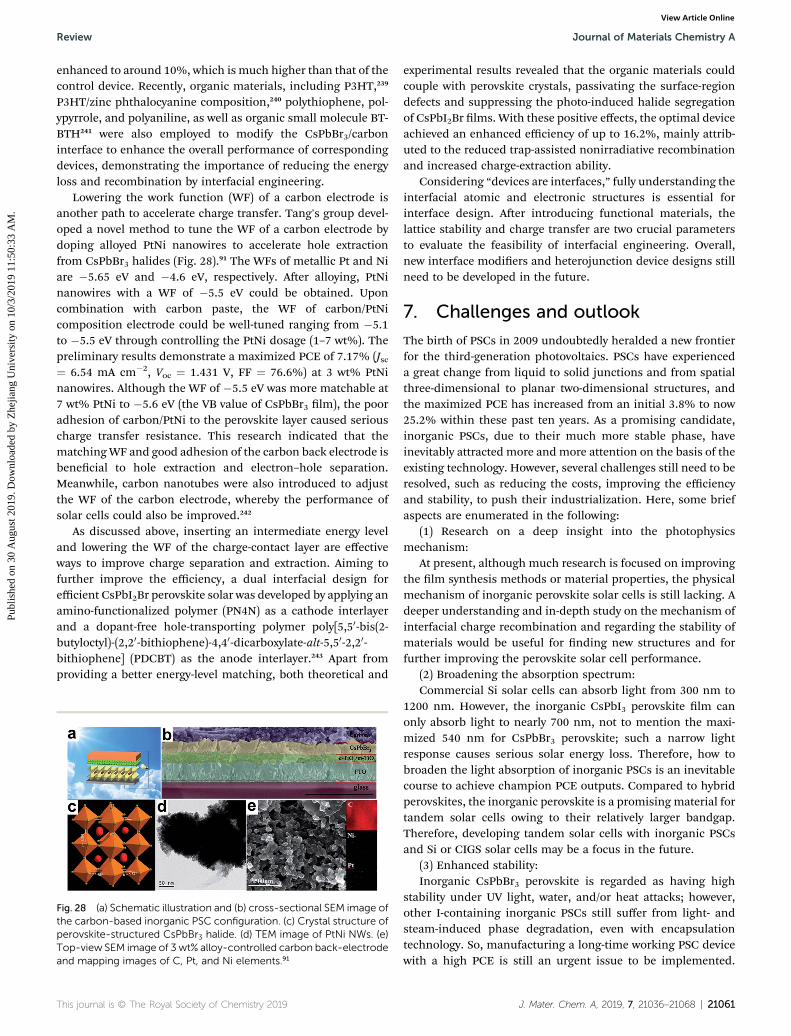
Review Journal of Materials Chemistry A
Publ
ishe
d on
30
Aug
ust 2
019.
Dow
nloa
ded
by Z
hejia
ng U
nive
rsity
on
10/3
/201
9 11
:50:
33 A
M.
View Article Online
enhanced to around 10%, which is much higher than that of thecontrol device. Recently, organic materials, including P3HT,239
P3HT/zinc phthalocyanine composition,240 polythiophene, pol-ypyrrole, and polyaniline, as well as organic small molecule BT-BTH241 were also employed to modify the CsPbBr3/carboninterface to enhance the overall performance of correspondingdevices, demonstrating the importance of reducing the energyloss and recombination by interfacial engineering.
Lowering the work function (WF) of a carbon electrode isanother path to accelerate charge transfer. Tang's group devel-oped a novel method to tune the WF of a carbon electrode bydoping alloyed PtNi nanowires to accelerate hole extractionfrom CsPbBr3 halides (Fig. 28).91 The WFs of metallic Pt and Niare �5.65 eV and �4.6 eV, respectively. Aer alloying, PtNinanowires with a WF of �5.5 eV could be obtained. Uponcombination with carbon paste, the WF of carbon/PtNicomposition electrode could be well-tuned ranging from �5.1to �5.5 eV through controlling the PtNi dosage (1–7 wt%). Thepreliminary results demonstrate a maximized PCE of 7.17% (Jsc¼ 6.54 mA cm�2, Voc ¼ 1.431 V, FF ¼ 76.6%) at 3 wt% PtNinanowires. Although the WF of �5.5 eV was more matchable at7 wt% PtNi to �5.6 eV (the VB value of CsPbBr3 lm), the pooradhesion of carbon/PtNi to the perovskite layer caused seriouscharge transfer resistance. This research indicated that thematchingWF and good adhesion of the carbon back electrode isbenecial to hole extraction and electron–hole separation.Meanwhile, carbon nanotubes were also introduced to adjustthe WF of the carbon electrode, whereby the performance ofsolar cells could also be improved.242
As discussed above, inserting an intermediate energy leveland lowering the WF of the charge-contact layer are effectiveways to improve charge separation and extraction. Aiming tofurther improve the efficiency, a dual interfacial design forefficient CsPbI2Br perovskite solar was developed by applying anamino-functionalized polymer (PN4N) as a cathode interlayerand a dopant-free hole-transporting polymer poly[5,50-bis(2-butyloctyl)-(2,20-bithiophene)-4,40-dicarboxylate-alt-5,50-2,20-bithiophene] (PDCBT) as the anode interlayer.243 Apart fromproviding a better energy-level matching, both theoretical and
Fig. 28 (a) Schematic illustration and (b) cross-sectional SEM image ofthe carbon-based inorganic PSC configuration. (c) Crystal structure ofperovskite-structured CsPbBr3 halide. (d) TEM image of PtNi NWs. (e)Top-view SEM image of 3 wt% alloy-controlled carbon back-electrodeand mapping images of C, Pt, and Ni elements.91
This journal is © The Royal Society of Chemistry 2019
experimental results revealed that the organic materials couldcouple with perovskite crystals, passivating the surface-regiondefects and suppressing the photo-induced halide segregationof CsPbI2Br lms. With these positive effects, the optimal deviceachieved an enhanced efficiency of up to 16.2%, mainly attrib-uted to the reduced trap-assisted nonirradiative recombinationand increased charge-extraction ability.
Considering “devices are interfaces,” fully understanding theinterfacial atomic and electronic structures is essential forinterface design. Aer introducing functional materials, thelattice stability and charge transfer are two crucial parametersto evaluate the feasibility of interfacial engineering. Overall,new interface modiers and heterojunction device designs stillneed to be developed in the future.
7. Challenges and outlook
The birth of PSCs in 2009 undoubtedly heralded a new frontierfor the third-generation photovoltaics. PSCs have experienceda great change from liquid to solid junctions and from spatialthree-dimensional to planar two-dimensional structures, andthe maximized PCE has increased from an initial 3.8% to now25.2% within these past ten years. As a promising candidate,inorganic PSCs, due to their much more stable phase, haveinevitably attracted more and more attention on the basis of theexisting technology. However, several challenges still need to beresolved, such as reducing the costs, improving the efficiencyand stability, to push their industrialization. Here, some briefaspects are enumerated in the following:
(1) Research on a deep insight into the photophysicsmechanism:
At present, although much research is focused on improvingthe lm synthesis methods or material properties, the physicalmechanism of inorganic perovskite solar cells is still lacking. Adeeper understanding and in-depth study on the mechanism ofinterfacial charge recombination and regarding the stability ofmaterials would be useful for nding new structures and forfurther improving the perovskite solar cell performance.
(2) Broadening the absorption spectrum:Commercial Si solar cells can absorb light from 300 nm to
1200 nm. However, the inorganic CsPbI3 perovskite lm canonly absorb light to nearly 700 nm, not to mention the maxi-mized 540 nm for CsPbBr3 perovskite; such a narrow lightresponse causes serious solar energy loss. Therefore, how tobroaden the light absorption of inorganic PSCs is an inevitablecourse to achieve champion PCE outputs. Compared to hybridperovskites, the inorganic perovskite is a promising material fortandem solar cells owing to their relatively larger bandgap.Therefore, developing tandem solar cells with inorganic PSCsand Si or CIGS solar cells may be a focus in the future.
(3) Enhanced stability:Inorganic CsPbBr3 perovskite is regarded as having high
stability under UV light, water, and/or heat attacks; however,other I-containing inorganic PSCs still suffer from light- andsteam-induced phase degradation, even with encapsulationtechnology. So, manufacturing a long-time working PSC devicewith a high PCE is still an urgent issue to be implemented.
J. Mater. Chem. A, 2019, 7, 21036–21068 | 21061

Journal of Materials Chemistry A Review
Publ
ishe
d on
30
Aug
ust 2
019.
Dow
nloa
ded
by Z
hejia
ng U
nive
rsity
on
10/3
/201
9 11
:50:
33 A
M.
View Article Online
Doping CsPbX3 with smaller radius ions has recently beenhighlighted as a promising way to achieve phase stability andreduce the trap density of the perovskite layer. Other strategies,such as solvent controlled lm growth, alloying a 2D perovskitecomponent into host perovskite, polymer-induced surfacepassivation, and interfacial engineering, all pave the way tostabilize CsPbI3.
(4) Environmentally friendly issues:Lead is a widely-used heavy metal element but is extremely
harmful to the human body, especially to children. A leadamount more than 10 mg dl�1 in blood can cause irreversibledamage to the mental development of children, so avoiding theusage of lead in perovskite solar cells is a signicant work.However, to date, highly efficient perovskite solar cells are allbased on toxic metal Pb, or on the partial substitution of Pb withother elements. In this regard, developing lead-free perovskitelight-absorbing layers is an important direction in the future.Although some researchers have made great efforts with lead-free perovskite solar cells, their photoelectric conversion effi-ciency is still low compared to Pb-based devices. Thus, furtherin-depth systematic research on materials and structures andthe preparation methods of new lead-free perovskite solar cellsis essential.
(5) Research on large-area devices:Scale-up and large-area processing technology has become
a tricky problem that must be resolved before commercializa-tion. Although some researchers have focused on large-areadevices, their lm uniformity is still poor as is their efficiency.So how to get high-efficiency large-area devices is still a greatchallenge. Tremendous progress has already been made inenhancing the performance of small-area cells (typically # 0.1cm2). However, many of the lm-making techniques (such asspin-coating and drop-casting) used in the laboratory do notsuit large-scale production. Spin-coating is currently the mostcommon lm-making strategy for inorganic perovskite layersbut not for large-area processing ($1 cm2). Besides, muchmaterial may be wasted during the process. Spraying andprinting methods seem to be promising methods for scale-up.However, clearly, scaling up the size of perovskite solar cellswithout signicant efficiency loss is a remaining challenge to beresolved.
(6) Flexible perovskite solar cells:With an aim to achieve the building of integrated photo-
voltaics, there have been many reports on organic–inorganicexible perovskite solar cells. However, insufficient studies onall-inorganic perovskite solar cells have been undertaken.Recently, Liu's group improved the quality of the perovskiteabsorber layer by adding dimethyl sulde, enhancing theefficiency of the exible perovskite solar cell.244 Zhao's groupdemonstrated a facile method to fabricate a high-performance all-inorganic CsPbI2Br perovskite solar cellthrough a one-step method under 100–130 �C low-temperature annealing process, which was benecial forassembly on exible substrate.176 Therefore, more researchshould be done to promote the development of exible inor-ganic perovskite solar cells.
21062 | J. Mater. Chem. A, 2019, 7, 21036–21068
8. Conclusions
The tremendous progress made in the development of inor-ganic perovskite solar cells convinces that inorganic perovskitesis a promising alternative to organic–inorganic perovskites, dueto their low-cost facile fabrication process and long-timestability. This review systematically summarizes the develop-ments of inorganic halide perovskite solar cells in respect ofcompositional engineering, lm-making methods, and inter-facial engineering methods. It also covered predicting theirlimited efficiency using the modied detailed balance modeland discussed the recombination mechanism. Finally, byidentifying new challenges, several outlooks are provided forfurther research and potential development in this area.
Conflicts of interest
There are no conicts to declare.
Acknowledgements
This work was supported by the National Natural ScienceFoundation of China (61774139, 21503202, 61604143), theFundamental Research Funds for the Central Universities(11618409, 21619311), and China Postdoctoral Science Foun-dation (55350315).
Notes and references
1 D. M. Chapin, C. S. Fuller and G. L. Pearson, J. Appl. Phys.,1954, 25, 676–677.
2 N. M. Haegel, R. Margolis, T. Buonassisi, D. Feldman,A. Froitzheim, R. Garabedian, M. Green, S. Glunz,H.-M. Henning, B. Holder, I. Kaizuka, B. Kroposki,K. Matsubara, S. Niki, K. Sakurai, R. A. Schindler,W. Tumas, E. R. Weber, G. Wilson, M. Woodhouse andS. Kurtz, Science, 2017, 356, 141–143.
3 Y. Ren, D. Sun, Y. Cao, H. N. Tsao, Y. Yuan,S. M. Zakeeruddin, P. Wang and M. Gratzel, J. Am. Chem.Soc., 2018, 140, 2405–2408.
4 N. Zhou, K. Prabakaran, B. Lee, S. H. Chang,B. Harutyunyan, P. Guo, M. R. Butler, A. Timalsina,M. J. Bedzyk, M. A. Ratner, S. Vegiraju, S. Yau, C.-G. Wu,R. P. H. Chang, A. Facchetti, M.-C. Chen and T. J. Marks,J. Am. Chem. Soc., 2015, 137, 4414–4423.
5 M. K. Brennaman, R. J. Dillon, L. Alibabaei, M. K. Gish,C. J. Dares, D. L. Ashford, R. L. House, G. J. Meyer,J. M. Papanikolas and T. J. Meyer, J. Am. Chem. Soc., 2016,138, 13085–13102.
6 Y. Saygili, M. Soderberg, N. Pellet, F. Cao, Y. Cao,A. B. Munoz-Garcıa, S. M. Zakeeruddin, N. Vlachopoulos,M. Pavone, G. Boschloo, L. Kavan, J. Moser, M. Gratzel,A. Hagfeldt and M. Freitag, J. Am. Chem. Soc., 2016, 138,15087–15096.
7 A. Kunzmann, S. Valero, A. E. Sepulveda, M. Rico-Santacruz,E. L. Jesus, R. Berenguer, J. Garcıa-Martınez, D. M. Guldi,
This journal is © The Royal Society of Chemistry 2019

Review Journal of Materials Chemistry A
Publ
ishe
d on
30
Aug
ust 2
019.
Dow
nloa
ded
by Z
hejia
ng U
nive
rsity
on
10/3
/201
9 11
:50:
33 A
M.
View Article Online
E. Serrano and R. D. Costa, Adv. Energy Mater., 2018, 12,1702583.
8 Z. Zhao, C. Lin, J. Tang and Z. Xia, Nano Energy, 2018, 49,193–199.
9 T. J. Barr and G. J. Meyer, ACS Energy Lett., 2017, 2, 2335–2340.
10 L. Song, W. Wang, S. Proller, D. M. Gonzalez, J. Schlipf,C. J. Schaffer, K. Peters, E. M. Herzig, S. Bernstorff,T. Bein, D. Fattakhova-Rohlng and P. Muller-Buschbaum, ACS Energy Lett., 2017, 2, 991–997.
11 P. Maisch, K. C. Tam, P. Schilinsky, H. Egelhaaf andC. J. Brabec, Sol. RRL, 2018, 2, 1800005.
12 B. Yang, M. A. Kolaczkowski, M. A. Brady, J. K. Keum,J. F. Browning, T. L. Chen and Y. Liu, Sol. RRL, 2018, 2,1700208.
13 Y. L. Lin, M. A. Fusella and B. P. Rand, Adv. Energy Mater.,2018, 8, 1702816.
14 C. Xie, A. Classen, A. Spath, X. Tang, J. Min, M. Meyer,C. Zhang, N. Li, A. Osvet, R. H. Fink and C. J. Brabec, Adv.Energy Mater., 2018, 8, 1702857.
15 I. Ramirez, M. Causa, Y. Zhong, N. Banerji and M. Riede,Adv. Energy Mater., 2018, 8, 1703551.
16 G. O. N. Ndjawa, K. R. Graham, S. Mollinger, D. M. Wu,D. Hani, R. Prasanna, B. D. Rose, S. Dey, L. Yu,J. Bredas, M. D. McGehee, A. Salleo and A. Amassian, Adv.Energy Mater., 2017, 7, 1601995.
17 N. Li, I. McCulloch and C. J. Brabec, Energy Environ. Sci.,2018, 11, 1355–1361.
18 S. Chang, P. Cheng, G. Li and Y. Yang, Joule, 2018, 2, 1–16.19 H. B. Naveed and W. Ma, Joule, 2018, 2, 621–641.20 S. M. Menke, N. A. Ran, G. C. Bazan and R. H. Friend, Joule,
2016, 2, 25–35.21 L. E. Garner, A. Bera, B. W. Larson, D. P. Ostrowski, A. J. Pal
and W. A. Braunecker, ACS Energy Lett., 2017, 2, 1556–1563.22 V. V. Duzhko, B. Dunham, S. J. Rosa, M. D. Cole, A. Paul,
Z. A. Page, C. Dimitrakopoulos and T. Emrick, ACS EnergyLett., 2017, 2, 957–963.
23 J. Jean, T. S. Mahony, D. Bozyigit, M. Sponseller,J. Holovsky, M. G. Bawendi and V. Bulovic, ACS EnergyLett., 2017, 2, 2616–2624.
24 L. Tan, P. Li, B. Sun, M. Chaker and D. Ma, ACS Energy Lett.,2017, 2, 1573–1585.
25 S. Pradhan, A. Stavrinadis, S. Gupta, S. Christodoulou andG. Konstantatos, ACS Energy Lett., 2017, 2, 1444–1449.
26 F. Wang, H. Wang, X. Liu, D. Wu, K. Jiang, Q. Li and D. Xu,Adv. Energy Mater., 2018, 8, 1800136.
27 S. Chen, Y. Wang, Q. Liu, G. Shi, Z. Liu, K. Lu, L. Han,X. Ling, H. Zhang, S. Cheng and W. Ma, Adv. EnergyMater., 2017, 8, 1701194.
28 S. Baek, S. Lee, J. H. Song, C. Kim, Y. Ha, H. Shin, H. Kim,S. Jeong and J. Lee, Energy Environ. Sci., 2018, 11, 2078–2084.
29 Y. Wang, Q. Zhang, F. Huang, Z. Li, Y. Zheng, X. Tao andG. Cao, Nano Energy, 2018, 44, 135–143.
30 J. M. Kim, S. Kim, D. H. Shin, S. W. Seo, H. S. Lee, J. H. Kim,C. W. Jang, S. S. Kang, S. Choi, G. Y. Kwak, K. J. Kim, H. Leeand H. Lee, Nano Energy, 2018, 43, 124–129.
This journal is © The Royal Society of Chemistry 2019
31 J.-H. Im, C.-R. Lee, J.-W. Lee, S.-W. Park and N.-G. Park,Nanoscale, 2011, 3, 4088–4093.
32 W. Zhang, G. E. Eperon and H. J. Snaith, Nat. Energy, 2016,1, 16048.
33 M. A. Green and A. Ho-Baillie, ACS Energy Lett., 2017, 2, 822–830.
34 N. J. Jeon, H. Na, E. H. Jung, T.-Y. Yang, Y. G. Lee, G. Kim,H.-W. Shin, S. I. Seok, J. Lee and J. Seo, Nat. Energy, 2018, 3,682–689.
35 R. Mastria, S. Colella, A. Qualtieri, A. Listorti, G. Giglia andA. Rizzo, Nanoscale, 2017, 9, 3889–3897.
36 A. Ummadisingu, L. Steier, J. Y. Seo, T. Matsui, A. Abate,W. Tress and M. Gratzel, Nature, 2017, 545, 208–212.
37 N. Ahn, D.-Y. Son, I.-H. Jang, S. M. Kang, M. Choi andN.-G. Park, J. Am. Chem. Soc., 2015, 137, 8696–8699.
38 A. Kojima, K. Teshima, Y. Shirai and T. Miyasaka, J. Am.Chem. Soc., 2009, 131, 6050–6051.
39 W. S. Yang, B. W. Park, E. H. Jung, N. J. Jeon, Y. C. Kim,D. U. Lee, S. S. Shin, J. Seo, E. K. Kim, J. H. Noh andS. I. Seok, Science, 2017, 356, 1376–1379.
40 E. H. Jung, N. J. Jeon, E. Y. Park, C. S. Moon, T. J. Shin,T.-Y. Yang, J. H. Noh and J. Seo, Nature, 2019, 567, 511–515.
41 Q. Jiang, Y. Zhao, X. Zhang, X. Yang, Y. Chen, Z. Chu, Q. Ye,X. Li, Z. Yin and J. You, Nat. Photonics, 2019, 13, 460–466.
42 M. Kim, G.-H. Kim, T. K. Lee, I. W. Choi, H. W. Choi, Y. Jo,Y. J. Yoon, J. W. Kim, J. Lee, D. Huh, H. Lee, S. K. Kwak,J. Y. Kim and D. S. Kim, Joule, 2019, DOI: 10.1016/j.joule.2019.06.014.
43 J. Burschka, N. Pellet, S. J. Moon, R. Humphry-Baker,P. Gao, M. K. Nazeeruddin and M. Gratzel, Nature, 2013,499, 316–319.
44 H. Zhou, Q. Chen, G. Li, S. Luo, T.-b. Song, H.-S. Duan,Z. Hong, J. You and Y. Yang, Science, 2014, 345, 542–546.
45 N. J. Jeon, J. H. Noh, W. S. Yang, Y. C. Kim, S. Ryu, J. Seo andS. I. Seok, Nature, 2015, 517, 476–480.
46 W. S. Yang, J. H. Noh, N. J. Jeon, Y. C. Kim, S. Ryu, J. Seo andS. I. Seok, Science, 2015, 348, 1234–1237.
47 https://www.nrel.gov/pv/assets/pdfs/best-research-cell-efficiencies.20190802.pdf.
48 B. Cai, Y. Xing, Z. Yang, W.-H. Zhang and J. Qiu, EnergyEnviron. Sci., 2013, 6, 1480–1485.
49 S. Pang, H. Hu, J. Zhang, S. Lv, Y. Yu, F. Wei, T. Qin, H. Xu,Z. Liu and G. Cui, Chem. Mater., 2014, 26, 1485–1491.
50 J. Tong, Z. Song, D. H. Kim, X. Chen, C. Chen,A. F. Palmstrom, P. F. Ndione, M. O. Reese,S. P. Duneld, O. G. Reid, J. Liu, F. Zhang, S. P. Harvey,Z. Li, S. T. Christensen, G. Teeter, D. Zhao, M. M. Al-Jassim, M. F. A. M. van Hest, M. C. Beard, S. E. Shaheen,J. J. Berry, Y. Yan and K. Zhu, Science, 2019, 364, 475–479.
51 A. A. Zhumekenov, M. I. Saidaminov, M. A. Haque,E. Alarousu, S. P. Sarmah, B. Murali, I. Dursun,X.-H. Miao, A. L. Abdelhady, T. Wu, O. F. Mohammed andO. M. Bakr, ACS Energy Lett., 2016, 1, 32–37.
52 Z. Wang, Z. Shi, T. Li, Y. Chen andW. Huang, Angew. Chem.,Int. Ed., 2017, 56, 1190–1212.
53 Q. A. Akkerman, G. Raino, M. V. Kovalenko and L. Manna,Nat. Mater., 2018, 17, 394–405.
J. Mater. Chem. A, 2019, 7, 21036–21068 | 21063

Journal of Materials Chemistry A Review
Publ
ishe
d on
30
Aug
ust 2
019.
Dow
nloa
ded
by Z
hejia
ng U
nive
rsity
on
10/3
/201
9 11
:50:
33 A
M.
View Article Online
54 S. Ahmad, P. K. Kanaujia, W. Niu, J. J. Baumberg andG. V. Prakash, ACS Appl. Mater. Interfaces, 2014, 6, 10238–10247.
55 T. Leijtens, G. E. Eperon, S. Pathak, A. Abate, M. M. Lee andH. J. Snaith, Nat. Commun., 2013, 4, 2885.
56 B. Conings, J. Drijkoningen, N. Gauquelin, A. Babayigit,J. Haen, L. D'Olieslaeger, A. Ethirajan, J. Verbeeck,J. Manca, E. Mosconi, F. D. Angelis and H.-G. Boyen, Adv.Energy Mater., 2015, 5, 1500477.
57 E. J. Juarez-Perez, Z. Hawash, S. R. Raga, L. K. Ono and Y. Qi,Energy Environ. Sci., 2016, 9, 3406–3410.
58 A. Ho-Baillie, M. Zhang, C. F. J. Lau, F.-J. Ma and S. Huang,Joule, 2019, 3, 938–955.
59 H. Chen, S. Xiang, W. Li, H. Liu, L. Zhu and S. Yang, Sol.RRL, 2018, 2, 1700188.
60 C. C. Stoumpos, C. D. Malliakas andM. G. Kanatzidis, Inorg.Chem., 2013, 52, 9019–9038.
61 C. C. Stoumpos, C. D. Malliakas, J. Peters, Z. Liu,M. Sebastian, J. Im, T. C. Chasapis, A. C. Wibowo,D. Y. Chung and A. J. Freeman, Cryst. Growth Des., 2013,13, 2722–2727.
62 H. L. Wells, Z. Anorg. Chem., 1893, 3, 195.63 B. Tang, H. Dong, L. Sun, W. Zheng, Q. Wang, F. Sun,
X. Jiang, A. Pan and L. Zhang, ACS Nano, 2017, 11, 10681–10688.
64 X. Tang, Z. Hu, W. Chen, X. Xing, Z. Zang, W. Hu, J. Qiu,J. Du, Y. Leng, X. Jiang and L. Mai, Nano Energy, 2016, 28,462–468.
65 H. Zhou, S. Yuan, X. Wang, T. Xu, X. Wang, H. Li, W. Zheng,P. Fan, Y. Li, L. Sun and A. Pan, ACS Nano, 2017, 11, 1189–1195.
66 D. Pan, Y. Fu, J. Chen, K. J. Czech, J. C. Wright and S. Jin,Nano Lett., 2018, 18, 1807–1813.
67 T. Yang, Y. Zheng, Z. Du, W. Liu, Z. Yang, F. Gao, L. Wang,K.-C. Chou, X. Hou and W. Yang, ACS Nano, 2018, 12, 1611–1617.
68 W. J. Yin, Y. F. Yan and S. H. Wei, J. Phys. Chem. Lett., 2014,5, 3625–3631.
69 P. Cottingham and R. L. Brutchey, Chem. Mater., 2016, 28,7574–7577.
70 J. Liang, P. Zhao, C. Wang, Y. Wang, Y. Hu, G. Zhu, L. Ma,J. Liu and Z. Jin, J. Am. Chem. Soc., 2017, 139, 14009–14012.
71 J.-P. Correa-Baena, A. Abate, M. Saliba, W. Tress, T. JesperJacobsson, M. Gratzel and A. Hagfeldt, Energy Environ.Sci., 2017, 10, 710–727.
72 Z. Cheng and J. Lin, CrystEngComm, 2010, 12, 2646–2662.73 W. A. Dunlap-Shohl, Y. Zhou, N. P. Padture and D. B. Mitzi,
Chem. Rev., 2019, 119, 3193–3295.74 W. Travis, E. N. K. Glover, H. Bronstein, D. O. Scanlon and
R. G. Palgrave, Chem. Sci., 2016, 7, 4548–4556.75 B. Saparov and D. B. Mitzi, Chem. Rev., 2016, 116, 4558–
4596.76 C. Li, X. Lu, W. Ding, L. Feng, Y. Gao and Z. Guo, Acta
Crystallogr., Sect. B: Struct. Sci., 2008, 64, 702–707.77 Y. Zhou and Y. Zhao, Energy Environ. Sci., 2019, 12, 1495–
1511.
21064 | J. Mater. Chem. A, 2019, 7, 21036–21068
78 N. Aristidou, C. Eames, I. Sanchez-Molina, X. Bu, J. Kosco,M. S. Islam and S. A. Haque, Nat. Commun., 2017, 8, 15218.
79 N. Arora, M. I. Dar, A. Hinderhofer, N. Pellet, F. Schreiber,S. M. Zakeeruddin and M. Gratzel, Science, 2017, 358,768–771.
80 E. H. Anaraki, A. Kermanpur, M. T. Mayer, L. Steier,T. Ahmed, S.-H. Turren-Cruz, J. Seo, J. Luo,S. M. Zakeeruddin, W. R. Tress, T. Edvinsson, M. Gratzel,A. Hagfeldt and J.-P. Correa-Baena, ACS Energy Lett., 2018,34, 773–778.
81 B. O'Regan and M. Gratzel, Nature, 1991, 353, 737–739.82 W. Zhang, M. Saliba, S. D. Stranks, Y. Sun, X. Shi,
U. Wiesner and H. J. Snaith, Nano Lett., 2013, 13, 4505–4510.
83 J. J. Choi, X. Yang, Z. M. Norman, S. J. L. Billinge andJ. S. Owen, Nano Lett., 2014, 14, 127–133.
84 M. Kulbak, D. Cahen and G. Hodes, J. Phys. Chem. Lett.,2015, 6, 2452–2456.
85 G. E. Eperon, G. M. Paterno, R. J. Sutton, A. Zampetti,A. A. Haghighirad, F. Cacialli and H. J. Snaith, J. Mater.Chem. A, 2015, 3, 19688–19695.
86 X. Chang, W. Li, L. Zhu, H. Liu, H. Geng, S. Xiang, J. Liu andH. Chen, ACS Appl. Mater. Interfaces, 2016, 8, 33649–33655.
87 P. Luo, Y. Zhou, S. Zhou, Y. Lu, C. Xu, W. Xia and L. Sun,Chem. Eng. J., 2018, 343, 146–154.
88 J. Liang, C. Wang, Y. Wang, Z. Xu, Z. Lu, Y. Ma, H. Zhu,Y. Hu, C. Xiao, X. Yi, G. Zhu, H. Lv, L. Ma, T. Chen,Z. Tie, Z. Jin and J. Liu, J. Am. Chem. Soc., 2016, 138,15829–15832.
89 J. Duan, Y. Zhao, B. He and Q. Tang, Angew. Chem., Int. Ed.,2018, 57, 3787–3791.
90 Y. Li, J. Duan, H. Yuan, Y. Zhao, B. He and Q. Tang, Sol. RRL,2018, 2, 1800164.
91 J. Ding, Y. Zhao, J. Duan, B. He and Q. Tang, ChemSusChem,2018, 11, 1432–1437.
92 J. Ding, J. Duan, C. Guo and Q. Tang, J. Mater. Chem. A,2018, 6, 21999–22004.
93 H. Yuan, Y. Zhao, J. Duan, B. He, Z. Jiao and Q. Tang,Electrochim. Acta, 2018, 279, 84–90.
94 G. Liao, J. Duan, Y. Zhao and Q. Tang, Sol. Energy, 2018, 171,279–285.
95 H. Xu, J. Duan, Y. Zhao, Z. Jiao, B. He and Q. Tang, J. PowerSources, 2018, 399, 76–82.
96 H. Li, G. Tong, T. Chen, H. Zhu, G. Li, Y. Chang, L. Wangand Y. Jiang, J. Mater. Chem. A, 2018, 6, 14255–14261.
97 J. Duan, Y. Zhao, X. Yang, Y. Wang, B. He and Q. Tang, Adv.Energy Mater., 2018, 8, 1802346.
98 J. Duan, D. Dou, Y. Zhao, Y. Wang, X. Yang, H. Yuan, B. Heand Q. Tang, Mater. Today Energy, 2018, 10, 146–152.
99 Y. Zhao, J. Duan, H. Yuan, Y. Wang, X. Yang, B. He andQ. Tang, Sol. RRL, 2019, 3, 1800284.
100 H. Yuan, Y. Zhao, J. Duan, Y. Wang, X. Yang and Q. Tang, J.Mater. Chem. A, 2018, 6, 24324–24329.
101 G. Tong, T. Chen, H. Li, W. Song, Y. Chang, J. Liu, L. Yu,J. Xu, Y. Qi and Y. Jiang, Sol. RRL, 2019, 3, 1900030.
102 X. Li, Y. Tan, H. Lai, S. Li, Y. Chen, S. Li, P. Xu and J. Yang,ACS Appl. Mater. Interfaces, 2019, 11, 29746–29752.
This journal is © The Royal Society of Chemistry 2019
Review Journal of Materials Chemistry A
Publ
ishe
d on
30
Aug
ust 2
019.
Dow
nloa
ded
by Z
hejia
ng U
nive
rsity
on
10/3
/201
9 11
:50:
33 A
M.
View Article Online
103 G. Tong, T. Chen, H. Li, L. Qiu, Z. Liu, Y. Dang, W. Song,L. K. Ono, Y. Jiang and Y. Qi, Nano Energy, 2019, 65, 104015.
104 Q. S. Ma, S. J. Huang, X. M. Wen, M. A. Green andA. W. Y. Ho-Baillie, Adv. Energy Mater., 2016, 6, 1502202.
105 C. F. J. Lau, X. Deng, Q. Ma, J. Zheng, J. S. Yun, M. A. Green,S. Huang and A. W. Y. Ho-Baillie, ACS Energy Lett., 2016, 1,573–577.
106 C. Liu, W. Li, J. Chen, J. Fan, Y. Mai and R. E. I. Schropp,Nano Energy, 2017, 41, 75–83.
107 Y. Guo, X. Yin, J. Liu and W. Que, J. Mater. Chem. A, 2019, 7,19008–19016.
108 W. Zhu, Z. Zhang, W. Chai, Q. Zhang, D. Chen, Z. Lin,J. Chang, J. Zhang, C. Zhang and Y. Hao, ChemSusChem,2019, 12, 2318–2325.
109 N. Li, Z. Zhu, J. Li, A. K.-Y. Jen and L. Wang, Adv. EnergyMater., 2018, 8, 1800525.
110 Z. Wang, X. Liu, Y. Lin, Y. Liao, Q. Wei, H. Chen, J. Qiu,Y. Chen and Y. Zheng, J. Mater. Chem. A, 2019, 7, 2773–2779.
111 Y. Jiang, J. Yuan, Y. Ni, J. Yang, Y. Wang, T. Jiu, M. Yuan andJ. Chen, Joule, 2018, 2, 1–13.
112 W. Zhou, Y. Zhao, X. Zhou, R. Fu, Q. Li, Y. Zhao, K. Liu,D. Yu and Q. Zhao, J. Phys. Chem. Lett., 2017, 8, 4122–4143.
113 C. Lau, M. Zhang, X. Deng, J. Zheng, J. Bing, Q. Ma, J. Kim,L. Hu, M. A. Green, S. Huang and A. Ho-Baillie, ACS EnergyLett., 2017, 2, 2319–2325.
114 J. K. Nam, S. U. Chai, W. Cha, Y. J. Choi, W. Kim, M. S. Jung,J. Kwon, D. Kim and J. H. Park, Nano Lett., 2017, 17, 2028–2033.
115 C. Chen, H. Lin, K. Chiang, W. Tsai, Y. Huang, C. Tsao andH. Lin, Adv. Mater., 2017, 29, 1605290.
116 D. Bai, J. Zhang, Z. Jin, H. Bian, K. Wang, H.Wang, L. Liang,Q. Wang and S. Frank Liu, ACS Energy Lett., 2018, 3, 970–978.
117 L. Yan, Q. Xue, M. Liu, Z. Zhu, J. Tian, Z. Li, Z. Chen,Z. Chen, H. Yan, H. Yip and Y. Cao, Adv. Mater., 2018, 30,1802509.
118 J. S. Niezgoda, B. J. Foley, A. Z. Chen and J. J. Choi, ACSEnergy Lett., 2017, 2, 1043–1049.
119 J. Zhang, D. Bai, Z. Jin, H. Bian, K. Wang, J. Sun, Q. Wangand S. Liu, Adv. Energy Mater., 2018, 8, 1703246.
120 C. Liu, W. Li, C. Zhang, Y. Ma, J. Fan and Y. Mai, J. Am.Chem. Soc., 2018, 140, 3825–3828.
121 S. Mariotti, O. S. Hutter, L. J. Phillips, P. J. Yates, B. Kunduand K. Durose, ACS Appl. Mater. Interfaces, 2018, 10, 3750–3760.
122 Q. Zeng, X. Zhang, X. Feng, S. Lu, Z. Chen, X. Yong,S. A. T. Redfern, H. Wei, H. Wang, H. Shen, W. Zhang,W. Zheng, H. Zhang, J. S. Tse and B. Yang, Adv. Mater.,2018, 30, 1705393.
123 H. Bian, D. Bai, Z. Jin, J. Zhang, Q. Wang and S. Liu, Joule,2018, 2, 1500–1510.
124 W. Chen, H. Chen, G. Xu, R. Xue, S. Wang, Y. Li and Y. Li,Joule, 2019, 3, 191–204.
125 S. S. Mali, J. V. Patil and C. K. Hong, Nano Lett., 2019, DOI:10.1021/acs.nanolett.9b02277.
This journal is © The Royal Society of Chemistry 2019
126 H. Sun, J. Zhang, X. Gan, L. Yu, H. Yuan, M. Shang, C. Lu,D. Hou, Z. Hu, Y. Zhu and L. Han, Adv. Energy Mater., 2019,9, 1900896.
127 Y. Zhang, C. Wu, D. Wang, Z. Zhang, X. Qi, N. Zhu, G. Liu,X. Li, H. Hu, Z. Chen, L. Xiao and B. Qu, Sol. RRL, 2019, DOI:10.1002/solr.201900254.
128 A. Swarnkar, A. R. Marshall, E. M. Sanehira,B. D. Chernomordik, D. T. Moore, J. A. Christians,T. Chakrabarti and J. M. Luther, Science, 2016, 354, 92–95.
129 Y. Hu, F. Bai, X. Liu, Q. Ji, X. Miao, T. Qiu and S. Zhang, ACSEnergy Lett., 2017, 2, 2219–2227.
130 L. A. Frolova, D. V. Anokhin, A. A. Piryazev, S. Y. Luchkin,N. N. Dremova, K. J. Stevenson and P. A. Troshin, J. Phys.Chem. Lett., 2017, 8, 67–72.
131 T. S. Ripolles, K. Nishinaka, Y. Ogomi, Y. Miyata andS. Hayase, Sol. Energy Mater. Sol. Cells, 2016, 144, 532–536.
132 T. Zhang, M. I. Dar, G. Li, F. Xu, N. Guo, M. Gratzel andY. Zhao, Sci. Adv., 2017, 3, e1700841.
133 P. Luo, W. Xia, S. Zhou, L. Sun, J. Cheng, C. Xu and Y. Lu, J.Phys. Chem. Lett., 2016, 7, 3603–3608.
134 Q. Wang, X. Zheng, Y. Deng, J. Zhao, Z. Chen and J. Huang,Joule, 2017, 1, 371–382.
135 F. Li, Y. Pei, F. Xiao, T. Zeng, Z. Yang, J. Xu, J. Sun, B. Pengand M. Liu, Nanoscale, 2018, 10, 6318–6322.
136 J. Liao, H. Rao, B. Chen, D. Kuang and C. Su, J. Mater. Chem.A, 2017, 5, 2066–2072.
137 Y. Wang, T. Zhang, M. Kan, Y. Li, T. Wang and Y. Zhao,Joule, 2018, 2, 2065–2075.
138 B. Li, Y. Zhang, L. Fu, T. Yu, S. Zhou, L. Zhang and L. Yin,Nat. Commun., 2018, 9, 1076–1084.
139 P. Wang, X. Zhang, Y. Zhou, Q. Jiang, Q. Ye, Z. Chu, X. Li,X. Yang, Z. Yin and J. You, Nat. Commun., 2018, 9, 2225–2232.
140 Y. Wang, T. Zhang, M. Kan and Y. Zhao, J. Am. Chem. Soc.,2018, 140, 12345–12348.
141 K. Chen, Q. Zhong, W. Chen, B. Sang, Y. Wang, T. Yang,Y. Liu, Y. Zhang and H. Zhang, Adv. Funct. Mater., 2019,29, 1900991.
142 X. Ling, S. Zhou, J. Yuan, J. Shi, Y. Qian, B. W. Larson,Q. Zhao, C. Qin, F. Li, G. Shi, C. Stewart, J. Hu, X. Zhang,J. M. Luther, S. Duhm and W. Ma, Adv. Energy Mater.,2019, 9, 1900721.
143 H. Zhao, J. Xu, S. Zhou, Z. Li, B. Zhang, X. Xia, X. Liu, S. Daiand J. Yao, Adv. Funct. Mater., 2019, 29, 1808986.
144 Y. Wang, M. I. Dar, L. K. Ono, T. Zhang, M. Kan, Y. Li,L. Zhang, X. Wang, Y. Yang, X. Gao, Y. Qi, M. Gratzel andY. Zhao, Science, 2019, 365, 591–595.
145 J. Zhang, G. Hodes, Z. Jin and S. Liu, Angew. Chem., Int. Ed.,2019, DOI: 10.1002/anie.201901081.
146 Q. Chen, H. Zhou, Z. Hong, S. Luo, H.-S. Duan, H.-H. Wang,Y. Liu, G. Li and Y. Yang, J. Am. Chem. Soc., 2014, 136, 622–625.
147 L. Etgar, P. Gao, Z. Xue, Q. Peng, A. K. Chandiran, B. Liu,M. K. Nazeeruddin and M. Gratzel, J. Am. Chem. Soc.,2012, 134, 17396–17399.
148 D. Liu and T. L. Kelly, Nat. Photonics, 2013, 8, 133–138.
J. Mater. Chem. A, 2019, 7, 21036–21068 | 21065

Journal of Materials Chemistry A Review
Publ
ishe
d on
30
Aug
ust 2
019.
Dow
nloa
ded
by Z
hejia
ng U
nive
rsity
on
10/3
/201
9 11
:50:
33 A
M.
View Article Online
149 Y. Tong, E. Bladt, M. F. Ayggler, A. Manzi, K. Z. Milowska,V. A. Hintermayr, P. Docampo, S. Bals, A. S. Urban,L. Polavarapu and J. Feldmann, Angew. Chem., Int. Ed.,2016, 55, 13887–13892.
150 L. Protesescu, S. Yakunin, M. I. Bodnarchuk, F. Krieg,R. Caputo, C. H. Hendon, R. X. Yang, A. Walsh andM. V. Kovalenko, Nano Lett., 2015, 15, 3692–3696.
151 L. Huang, Q. Gao, L.-D. Sun, H. Dong, S. Shi, T. Cai, Q. Liaoand C.-H. Yan, Adv. Mater., 2018, 30, 1800596.
152 G. R. Yettapu, D. Talukdar, S. Sarkar, A. Swarnkar, A. Nag,P. Ghosh and P. Mandal, Nano Lett., 2016, 16(8), 4838–4848.
153 T. Shi, W.-J. Yin, F. Hong, K. Zhu and Y. Yan, Appl. Phys.Lett., 2015, 106, 103902.
154 J. Kang and L.-W. Wang, J. Phys. Chem. Lett., 2017, 8, 489–493.
155 F. Palazon, S. Dogan, S. Marras, F. Locardi, I. Nelli,P. Rastogi, M. Ferretti, M. Prato, R. Krahne andL. Manna, J. Phys. Chem. C, 2017, 121, 11956–11961.
156 J.-H. Cha, J. H. Han, W. Yin, C. Park, Y. Park, T. K. Ahn,J. H. Cho and D.-Y. Jung, J. Phys. Chem. Lett., 2017, 8,565–570.
157 X. Zhang, Z. Jin, J. Zhang, D. Bai, H. Bian, K. Wang, J. Sun,Q. Wang and S. F. Liu, ACS Appl. Mater. Interfaces, 2018, 10,7145–7154.
158 M. Aamir, T. Adhikari, M. Sher, N. Revaprasadu, W. Khalid,J. Akhtar and J.-M. Nunzi, New J. Chem., 2018, 42, 14104–14110.
159 Q. Ma, S. Huang, S. Chen, M. Zhang, C. F. J. Lau,M. N. Lockrey, H. K. Mulmudi, Y. Shan, J. Yao, J. Zheng,X. Deng, K. Catchpole, M. A. Green and A. W. Y. Ho-Baillie, J. Phys. Chem. C, 2017, 121, 19642–19649.
160 Q. Zhang, W. Zhu, D. Chen, Z. Zhang, Z. Lin, J. Chang,J. Zhang, C. Zhang and Y. Hao, ACS Appl. Mater.Interfaces, 2019, 11, 2997–3005.
161 R. J. Sutton, G. E. Eperon, L. Miranda, E. S. Parrott,B. A. Kamino, J. B. Patel, M. T. Horantner,M. B. Johnston, A. A. Haghighirad, D. T. Moore andH. J. Snaith, Adv. Energy Mater., 2016, 6, 1502458.
162 J. Liang, C. Wang, P. Zhao, Z. Lu, Y. Ma, Z. Xu, Y. Wang,H. Zhu, Y. Hu, G. Zhu, L. Ma, T. Chen, Z. Tie, J. Liu andZ. Jin, Nanoscale, 2017, 9, 11841–11846.
163 Z. Zeng, J. Zhang, X. Gan, H. Sun, M. Shang, D. Hou, C. Lu,R. Chen, Y. Zhu and L. Han, Adv. Energy Mater., 2018, 8,1801050.
164 W. Li, M. U. Rothmann, A. Liu, Z. Wang, Y. Zhang,A. R. Pascoe, J. Lu, L. Jiang, Y. Chen, F. Huang, Y. Peng,Q. Bao, J. Etheridge, U. Bach and Y.-B. Cheng, Adv. EnergyMater., 2017, 7, 1700946.
165 W. Zhu, Q. Zhang, D. Chen, Z. Zhang, Z. Lin, J. Chang,J. Zhang, C. Zhang and Y. Hao, Adv. Energy Mater., 2018,8, 1802080.
166 W. Zhua, W. Chai, Z. Zhang, D. Chen, J. Chang, S. Liu,J. Zhang, C. Zhang and Y. Hao, Org. Electron., 2019, 74,103–109.
167 W. Zhu, Z. Zhang, W. Chai, D. Chen, H. Xi, J. Chang,J. Zhang, C. Zhang and Y. Hao, ACS Appl. Energy Mater.,2019, 2, 5254–5262.
21066 | J. Mater. Chem. A, 2019, 7, 21036–21068
168 C. D. Bailie, M. G. Christoforo, J. P. Mailoa, A. R. Bowring,E. L. Unger, W. H. Nguyen, J. Burschka, N. Pellet, J. Z. Leeand M. Gratzel, Energy Environ. Sci., 2015, 8, 956–963.
169 T. Todorov, T. Gershon, O. Gunawan, C. Sturdevant andS. Guha, Appl. Phys. Lett., 2014, 105, 1441–1680.
170 P. Loper, S. J. Moon, S. M. de Nicolas, B. Niesen,M. Ledinsky, S. Nicolay, J. Bailat, J. H. Yum, S. D. Wolfand C. Ballif, Phys. Chem. Chem. Phys., 2015, 17, 1619–1629.
171 R. E. Beal, D. J. Slotcavage, T. Leijtens, A. R. Bowring,R. A. Belisle, W. H. Nguyen, G. F. Burkhard, E. T. Hokeand M. D. McGehee, J. Phys. Chem. Lett., 2016, 7, 746–751.
172 I. Yokota, J. Phys. Soc. Jpn., 1953, 8, 595–602.173 R. Gottesman, L. Gouda, B. S. Kalanoor, E. Haltzi, S. Tirosh,
E. Rosh-Hodesh, Y. Tischler, A. Zaban, C. Quarti,E. Mosconi and F. D. Angelis, J. Phys. Chem. Lett., 2015, 6,2332–2338.
174 H. Zhu, K. Miyata, Y. Fu, J. Wang, P. P. Joshi, D. Niesner,K. W. Williams, S. Jin and X.-Y. Zhu, Science, 2016, 353,1409–1413.
175 J. K. Nam, M. S. Jung, S. U. Chai, Y. J. Choi, D. Kim andJ. H. Park, J. Phys. Chem. Lett., 2017, 8, 2936–2940.
176 Y. Wang, T. Zhang, F. Xu, Y. Li and Y. Zhao, Sol. RRL, 2018,2, 1700180.
177 H. Rao, S. Ye, F. Gu, Z. Zhao, Z. Liu, Z. Bian and C. Huang,Adv. Energy Mater., 2018, 8, 1800758.
178 A. Marronnier, G. Roma, S. Boyer-Richard, L. Pedesseau,J. M. Jancu, Y. Bonnassieux, C. Katan, C. C. Stoumpos,M. G. Kanatzidis and J. Even, ACS Nano, 2018, 12, 3477–3486.
179 E. M. Sanehira, A. R. Marshall, J. A. Christians, S. P. Harvey,P. N. Ciesielski, L. M. Wheeler, P. Schulz, L. Y. Lin,M. C. Beard and J. M. Luther, Sci. Adv., 2017, 3, 10–18.
180 Q. Wang, Z. Jin, D. Chen, D. Bai, H. Bian, J. Sun, G. Zhu,G. Wang and S. Liu, Adv. Energy Mater., 2018, 8, 1800007.
181 J. Wei, H. Li, Y. Zhao, W. Zhou, R. Fu, Y. Leprince-Wang,D. Yu and Q. Zhao, Nano Energy, 2016, 26, 139–147.
182 L. Tan, C. Wang, M. Zeng and L. Fu, Small, 2017, 13,1603337.
183 S. N. Habisreutinger, T. Leijtens, G. E. Eperon,S. D. Stranks, R. J. Nicholas and H. J. Snaith, Nano Lett.,2014, 14, 5561–5568.
184 X. Ding, H. Chen, Y. Wu, S. Ma, S. Dai, S. Yang and J. Zhu, J.Mater. Chem. A, 2018, 6, 18258–18266.
185 K.Wang, Z. Jin, L. Liang, H. Bian, D. Bai, H.Wang, J. Zhang,Q. Wang and S. Liu, Nat. Commun., 2018, 9, 4544.
186 Z. Chen, J. J. Wang, Y. Ren, C. Yu and K. Shum, Appl. Phys.Lett., 2012, 101, 093901.
187 S. Gupta, T. Bendikov, G. Hodes and D. Cahen, ACS EnergyLett., 2016, 1, 1028–1033.
188 F. Wang, J. L. Ma, F. Y. Xie, L. K. Li, J. Chen, J. Fan andN. Zhao, Adv. Funct. Mater., 2016, 26, 3417–3423.
189 M. H. Kumar, S. Dharani, W. L. Leong, P. P. Boix,R. R. Prabhakar, T. Baikie, C. Shi, H. Ding, R. Ramesh,M. Asta, M. Graetzel, S. G. Mhaisalkar and N. Mathews,Adv. Mater., 2014, 26, 7122.
190 W. Li, J. Li, J. Li, J. Fan, Y. Mai and L. Wang, J. Mater. Chem.A, 2016, 4, 17104–17110.
This journal is © The Royal Society of Chemistry 2019

Review Journal of Materials Chemistry A
Publ
ishe
d on
30
Aug
ust 2
019.
Dow
nloa
ded
by Z
hejia
ng U
nive
rsity
on
10/3
/201
9 11
:50:
33 A
M.
View Article Online
191 D. Sabba, H. K. Mulmudi, R. R. Prabhakar,T. Krishnamoorthy, T. Baikie, P. P. Boix, S. Mhaisalkarand N. Mathews, J. Phys. Chem. C, 2015, 119, 1763.
192 K. P. Marshall, M. Walker, R. I. Walton and R. A. Hatton,Nat. Energy, 2016, 1, 16178.
193 T. Krishnamoorthy, H. Ding, C. Yan, W. L. Leong, T. Baikie,Z. Zhang, M. Sherburne, S. Li, M. Asta, N. Mathews andS. G. Mhaisalkar, J. Mater. Chem. A, 2015, 3, 23829–23832.
194 Q. Sun, H. Chen and W.-J. Yin, Chem. Mater., 2019, 31, 244–250.
195 X.-G. Zhao, J.-H. Yang, Y. Fu, D. Yang, Q. Xu, L. Yu,S.-H. Wei and L. Zhang, J. Am. Chem. Soc., 2017, 139,2630–2638.
196 W. Zhao, Z. Yao, F. Yu, D. Yang and S. Liu, Adv. Sci., 2018, 5,1700131.
197 S. Zou, Y. Liu, J. Li, C. Liu, R. Feng, F. Jiang, Y. Li, J. Song,H. Zeng, M. Hong and X. Chen, J. Am. Chem. Soc., 2017, 139,11443–11452.
198 M. Abdi-Jalebi, Z. Andaji-Garmaroudi, S. Cacovich,C. Stavrakas, B. Philippe, J. M. Richter, M. Alsari,E. P. Booker, E. M. Hutter, A. J. Pearson, S. Lilliu,T. J. Savenije, H. Rensmo, G. Divitini, C. Ducati,R. H. Friend and S. D. Stranks, Nature, 2018, 555, 497–501.
199 J.-W. Lee, D.-H. Kim, H.-S. Kim, S.-W. Seo, S. M. Cho andN.-G. Park, Adv. Energy Mater., 2015, 5, 1501310.
200 J. Liang, Z. Liu, L. Qiu, Z. Hawash, L. Meng, Z. Wu, Y. Jiang,L. K. Ono and Y. Qi, Adv. Energy Mater., 2018, 8, 1800504.
201 Y. Zhao, Y. Wang, J. Duan, X. Yang and Q. Tang, J. Mater.Chem. A, 2019, 7, 6877–6882.
202 C. F. J. Lau, X. Deng, J. Zheng, J. Kim, Z. Zhang, M. Zhang,J. Bing, B. Wilkinson, L. Hu, R. Patterson, S. Huang andA. Ho-Baillie, J. Mater. Chem. A, 2018, 6, 5580–5586.
203 C. Liu, W. Li, H. Li, H. Wang, C. Zhang, Y. Yang, X. Gao,Q. Xue, H. -L. Yip, J. Fan, R. E. I. Schropp and Y. Mai,Adv. Energy Mater., 2019, 9, 1803572.
204 Z. Guo, S. Zhao, A. Liu, Y. Kamata, S. Teo, S. Yang, Z. Xu,S. Hayase and T. Ma, ACS Appl. Mater. Interfaces, 2019, 11,19994–20003.
205 W. Xiang, Z. Wang, D. J. Kubicki, W. Tress, J. Luo,D. Prochowicz, S. Akin, L. Emsley, J. Zhou, G. Dietler,M. Gratzel and A. Hagfeldt, Joule, 2019, 3, 205–214.
206 W. S. Subhani, K. Wang, M. Du, X. Wang and S. Liu, Adv.Energy Mater., 2019, 9, 1803785.
207 Z. Wang, A. K. Baranwal, M. A. Kamarudin, Y. Kamata,C. H. Ng, M. Pandey, T. Ma and S. Hayase, J. Mater.Chem. A, 2019, DOI: 10.1039/C9TA05556H.
208 A. Swarnkar, W. J. Mir and A. Nag, ACS Energy Lett., 2018, 3,286–289.
209 R. E. Brandt, V. Stevanovic, D. S. Ginley and T. Buonassisi,MRS Commun., 2015, 5, 265.
210 M. I. Saidaminov, J. Kim, A. Jain, R. Quintero-Bermudez,H. Tan, G. Long, F. Tan, A. Johnston, Y. Zhao, O. Voznyyand E. H. Sargent, Nat. Energy, 2018, 3, 648–654.
211 J. T.-W. Wang, Z. Wang, S. Pathak, W. Zhang,D. W. deQuilettes, F. Wisnivesky-Rocca-Rivarola,J. Huang, P. K. Nayak, J. B. Patel, H. A. M. Yusof,Y. Vaynzof, R. Zhu, I. Ramirez, J. Zhang, C. Ducati,
This journal is © The Royal Society of Chemistry 2019
C. Grovenor, M. B. Johnston, D. S. Ginger, R. J. Nicholasand H. J. Snaith, Energy Environ. Sci., 2016, 9, 2892–2901.
212 H. S. Kim, C. R. Lee, J. H. Im, K. B. Lee, T. Moehl,A. Marchioro, S. J. Moon, R. Humphry-Baker, J. H. Yum,J. E. Moser, M. Gratzel and N. G. Park, Sci. Rep., 2012, 2, 591.
213 D. Bai, H. Bian, Z. Jin, H. Wang, L. Meng, Q. Wang andS. Liu, Nano Energy, 2018, 52, 408–415.
214 M. Liu, M. B. Johnston and H. J. Snaith, Nature, 2013, 501,395–398.
215 M. Wang, P. Zeng, S. Bai, J. Gu, F. Li, Z. Yang and M. Liu,Sol. RRL, 2018, 2, 1800217.
216 P. Teng, X. Han, J. Li, Y. Xu, L. Kang, Y. Wang, Y. Yang andT. Yu, ACS Appl. Mater. Interfaces, 2018, 10, 9541–9546.
217 Q. A. Akkerman, M. Gandini, F. D. Stasio, P. Rastogi,F. Palazon, G. Bertoni, J. M. Ball, M. Prato, A. Petrozzaand L. Manna, Nat. Energy, 2016, 2, 16194.
218 J. B. Hoffman, G. Zaiats, I. Wappes and P. V. Kamat, Chem.Mater., 2017, 29, 9767–9774.
219 A. Barrows, A. Pearson, C. Kwak, A. Dunbar, A. Buckley andD. Lidzey, Energy Environ. Sci., 2014, 7, 2944–2951.
220 X. Xia, W. Wu, H. Li, B. Zheng, Y. Xue, J. Xu, D. Zhang,C. Gao and X. Liu, RSC Adv., 2016, 6, 14792–14798.
221 X. Liu, X. Tan, Z. Liu, H. Ye, B. Sun, T. Shi, Z. Tang andG. Liao, Nano Energy, 2019, 56, 184–195.
222 W. E. I. Sha, X. Ren, L. Chen and W. C. H. Choy, Appl. Phys.Lett., 2015, 106, 221104.
223 W. Shockley and H. J. Queisser, J. Appl. Phys., 1961, 32, 510.224 T. Tiedje, E. Yablonovitch, G. D. Cody and B. G. Brooks,
IEEE Trans. Electron Devices, 1984, 31, 711–716.225 H. R. Stuart and D. G. Hall, J. Opt. Soc. Am. A, 1997, 14,
3001–3008.226 R. T. Ross, J. Chem. Phys., 1967, 46, 4590–4593.227 A. Braun, E. A. Katz, D. Feuermann, B. M. Kayes and
J. M. Gordon, Energy Environ. Sci., 2013, 6, 1499–1503.228 W. E. I. Sha, H. Zhang, Z. S. Wang, H. L. Zhu, X. Ren, F. Lin,
A. K.-Y. Jen and W. C. H. Choy, Adv. Energy Mater., 2018, 8,1701586.
229 P. Zhu, C. Chen, S. Gu, R. Lin and J. Zhu, Sol. RRL, 2018, 2,1700224.
230 J. Shi, X. Xu, D. Li and Q. Meng, Small, 2015, 11, 2472–2486.231 Z. Guo, S. Teo, Z. Xu, C. Zhang, Y. Kamata, S. Hayase and
T. Ma, J. Mater. Chem. A, 2019, 7, 1227–1232.232 H. Tan, A. Jain, O. Voznyy, X. Lan, F. P. G. de Arquer,
J. Z. Fan, R. Quintero-Bermudez, M. Yuan, B. Zhang,Y. Zhao, F. Fan, P. Li, L. N. Quan, Y. Zhao, Z.-H. Lu,Z. Yang, S. Hoogland and E. H. Sargent, Science, 2017,355, 722–726.
233 Y. Xiao, G. Han, Y. Li, M. Li and J. Wu, J. Mater. Chem. A,2014, 2, 16856–16862.
234 S. Ito, S. Tanaka, K. Manabe and H. Nishino, J. Phys. Chem.C, 2014, 118, 16995–17000.
235 G. S. Han, H. S. Chung, B. J. Kim, D. H. Kim, J. W. Lee,B. S. Swain, K. Mahmood, J. S. Yoo, N. G. Park, J. H. Leeand H. S. Jung, J. Mater. Chem. A, 2015, 3, 9160–9164.
236 Y. Ogomi, K. Kukihara, Q. Shen, T. Toyoda, K. Yoshino,S. Pandey, H. Momose and S. Hayase, ChemPhysChem,2014, 15, 1062–1069.
J. Mater. Chem. A, 2019, 7, 21036–21068 | 21067

Journal of Materials Chemistry A Review
Publ
ishe
d on
30
Aug
ust 2
019.
Dow
nloa
ded
by Z
hejia
ng U
nive
rsity
on
10/3
/201
9 11
:50:
33 A
M.
View Article Online
237 M. Cha, P. Da, J. Wang, W. Wang, Z. Chen, F. Xiu, G. Zhengand Z.-S. Wang, J. Am. Chem. Soc., 2016, 138, 8581–8587.
238 Q. Li, J. Bai, T. Zhang, C. Nie, J. Duan and Q. Tang, Chem.Commun., 2018, 54, 9575–9578.
239 G. Wang, W. Dong, A. Gurung, K. Chen, F. Wu, Q. He,R. Pathak and Q. Qiao, J. Power Sources, 2019, 432, 48–54.
240 Y. Liu, B. He, J. Duan, Y. Zhao, Y. Ding, M. Tang, H. Chenand Q. Tang, J. Mater. Chem. A, 2019, 7, 12635–12644.
21068 | J. Mater. Chem. A, 2019, 7, 21036–21068
241 Y. Zhao, T. Liu, F. Ren, J. Duan, Y. Wang, X. Yang, Q. Li andQ. Tang, Mater. Chem. Front., 2018, 2, 2239–2244.
242 G. Liao, Y. Zhao, J. Duan, H. Yuan, Y. Wang, X. Yang, B. Heand Q. Tang, Dalton Trans., 2018, 47, 15283–15287.
243 J. Tian, Q. Xue, X. Tang, Y. Chen, N. Li, Z. Hu, T. Shi,X. Wang, F. Huang, C. J. Brabec, H. -L. Yip and Y. Cao,Adv. Mater., 2019, 31, 1901152.
244 J. Feng, X. Zhu, Z. Yang, X. Zhang, J. Niu, Z. Wang, S. Zuo,S. Priya, S. Liu and D. Yang, Adv. Mater., 2018, 30, 1801418.
This journal is © The Royal Society of Chemistry 2019