introduction to nand in embedded systems · migration from nor to nand. ... besides the advantage...
TRANSCRIPT
Introduction to NAND in Embedded Systems
1P/N: AN0269 REV. 2, FEB. 20, 2014
TECHNICAL NOTE
IntroductionNAND Flash memory has been widely adopted in Embedded systems as a memory of choice. NAND Flash is often used as a NOR Flash replacement for cost reasons (and sometimes also for performance reasons). However, NOR and NAND Flash have architectural and reliability differences that complicate system migration from NOR to NAND.
This technical note will introduce NAND Flash memory technology with a focus on Single Level Cell (SLC) products which are predominantly used in embedded systems.
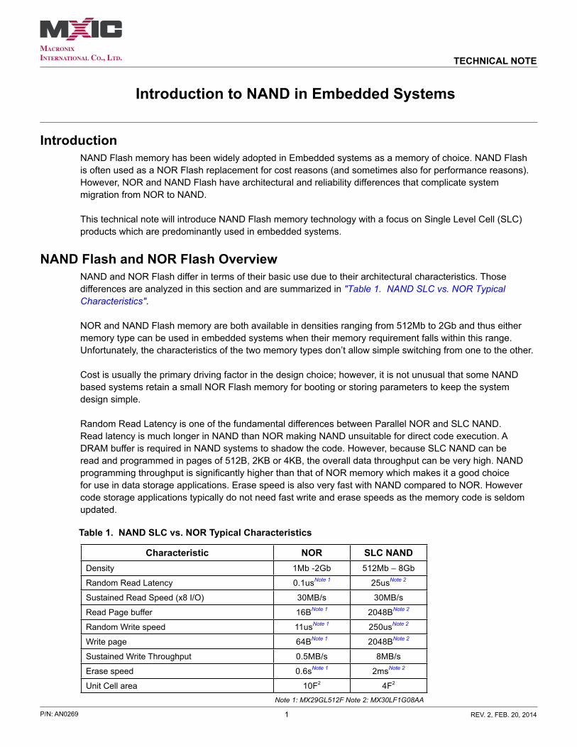
NAND Flash and NOR Flash OverviewNAND and NOR Flash differ in terms of their basic use due to their architectural characteristics. Those differences are analyzed in this section and are summarized in "Table 1. NAND SLC vs. NOR Typical Characteristics".
NOR and NAND Flash memory are both available in densities ranging from 512Mb to 2Gb and thus either memory type can be used in embedded systems when their memory requirement falls within this range. Unfortunately, the characteristics of the two memory types don’t allow simple switching from one to the other.
Cost is usually the primary driving factor in the design choice; however, it is not unusual that some NAND based systems retain a small NOR Flash memory for booting or storing parameters to keep the system design simple.
Random Read Latency is one of the fundamental differences between Parallel NOR and SLC NAND. Read latency is much longer in NAND than NOR making NAND unsuitable for direct code execution. A DRAM buffer is required in NAND systems to shadow the code. However, because SLC NAND can be read and programmed in pages of 512B, 2KB or 4KB, the overall data throughput can be very high. NAND programming throughput is significantly higher than that of NOR memory which makes it a good choice for use in data storage applications. Erase speed is also very fast with NAND compared to NOR. However code storage applications typically do not need fast write and erase speeds as the memory code is seldom updated.
Table 1. NAND SLC vs. NOR Typical Characteristics
Characteristic NOR SLC NANDDensity 1Mb -2Gb 512Mb – 8Gb
Random Read Latency 0.1usNote 1 25usNote 2
Sustained Read Speed (x8 I/O) 30MB/s 30MB/s
Read Page buffer 16BNote 1 2048BNote 2
Random Write speed 11usNote 1 250usNote 2
Write page 64BNote 1 2048BNote 2
Sustained Write Throughput 0.5MB/s 8MB/s
Erase speed 0.6sNote 1 2msNote 2
Unit Cell area 10F2 4F2
Note 1: MX29GL512F Note 2: MX30LF1G08AA
2P/N: AN0269 REV. 2, FEB. 20, 2014
TECHNICAL NOTE
Besides the advantage in terms of area (due to the NAND cell structure), NAND technology is more easily scaled (suitable for shrinking to more advanced technology nodes). A technology roadmap for NAND and NOR is shown in "Table 2. NAND vs. NOR Technology Roadmap (ITRS)". The forecast is based on the hypothesis that at least two suppliers will be in production with the given technology. The technology shown for NAND refers to high density (MLC) products. SLC NAND products are usually produced by employing one or two technology nodes behind the mainstream technology. Moreover, one can readily observe that very few major industry Flash suppliers have any plan to migrate below 45nm for NOR in the coming years.
Table 2. NAND vs. NOR Technology Roadmap (ITRS)
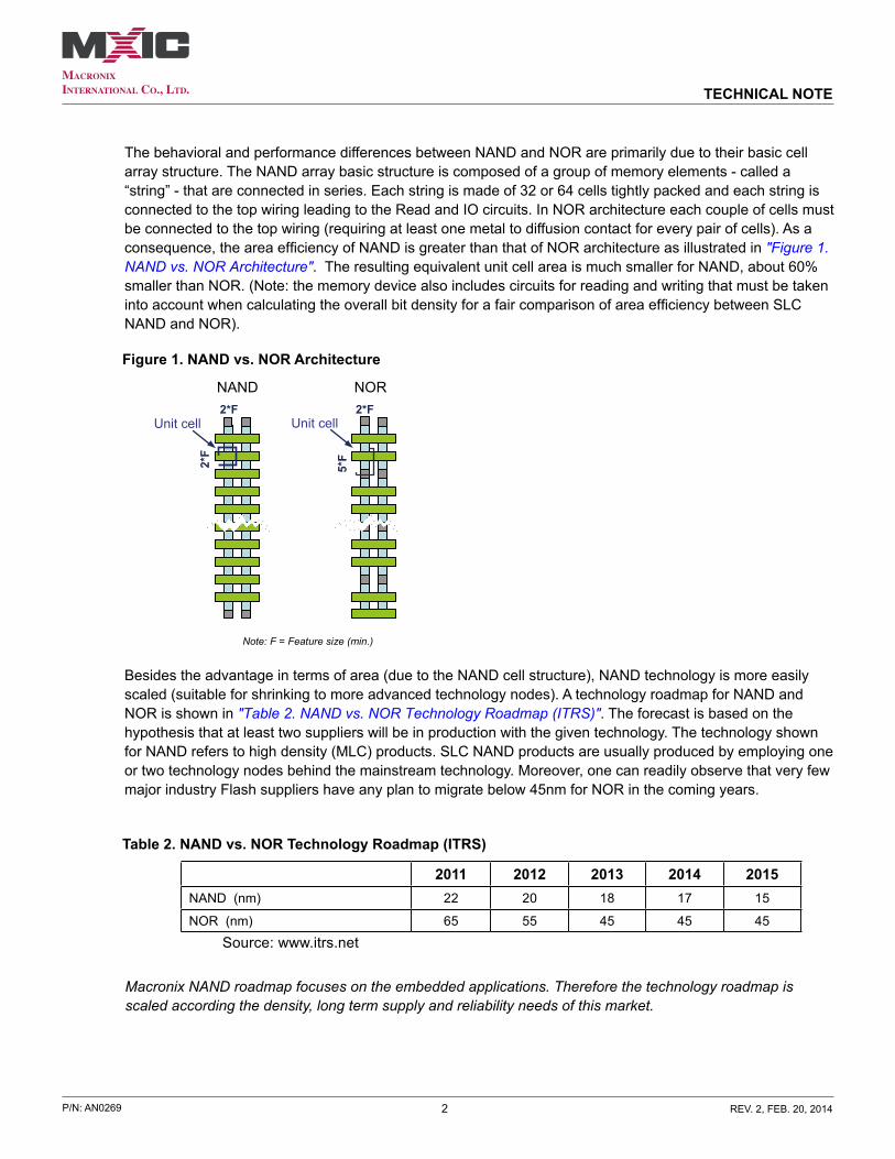
The behavioral and performance differences between NAND and NOR are primarily due to their basic cell array structure. The NAND array basic structure is composed of a group of memory elements - called a “string” - that are connected in series. Each string is made of 32 or 64 cells tightly packed and each string is connected to the top wiring leading to the Read and IO circuits. In NOR architecture each couple of cells must be connected to the top wiring (requiring at least one metal to diffusion contact for every pair of cells). As a consequence, the area efficiency of NAND is greater than that of NOR architecture as illustrated in "Figure 1. NAND vs. NOR Architecture". The resulting equivalent unit cell area is much smaller for NAND, about 60% smaller than NOR. (Note: the memory device also includes circuits for reading and writing that must be taken into account when calculating the overall bit density for a fair comparison of area efficiency between SLC NAND and NOR).
Figure 1. NAND vs. NOR Architecture
2*F
2*F
2*F
5*F
NAND NOR
Unit cell Unit cell
Note: F = Feature size (min.)
2011 2012 2013 2014 2015NAND (nm) 22 20 18 17 15
NOR (nm) 65 55 45 45 45
Macronix NAND roadmap focuses on the embedded applications. Therefore the technology roadmap is scaled according the density, long term supply and reliability needs of this market.
Source: www.itrs.net
3P/N: AN0269 REV. 2, FEB. 20, 2014
TECHNICAL NOTE
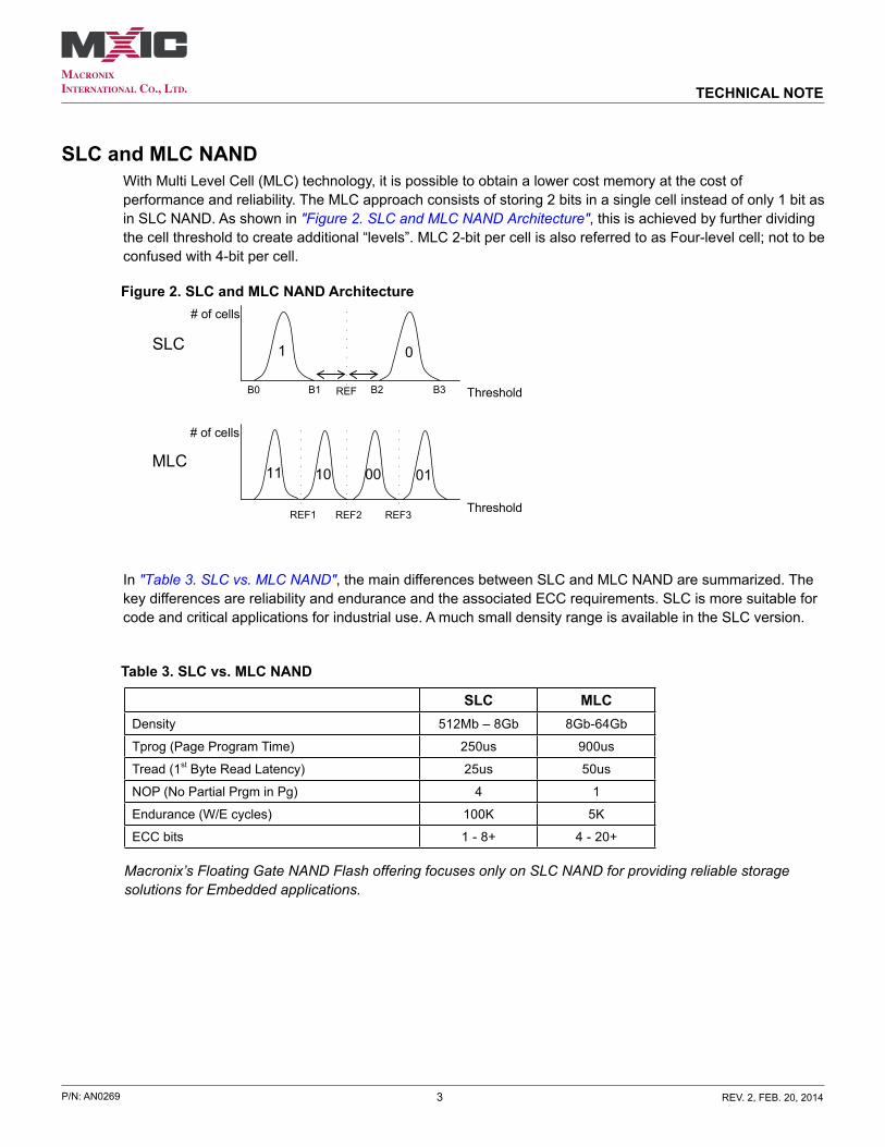
SLC and MLC NANDWith Multi Level Cell (MLC) technology, it is possible to obtain a lower cost memory at the cost of performance and reliability. The MLC approach consists of storing 2 bits in a single cell instead of only 1 bit as in SLC NAND. As shown in "Figure 2. SLC and MLC NAND Architecture", this is achieved by further dividing the cell threshold to create additional “levels”. MLC 2-bit per cell is also referred to as Four-level cell; not to be confused with 4-bit per cell.
Figure 2. SLC and MLC NAND Architecture
In "Table 3. SLC vs. MLC NAND", the main differences between SLC and MLC NAND are summarized. The key differences are reliability and endurance and the associated ECC requirements. SLC is more suitable for code and critical applications for industrial use. A much small density range is available in the SLC version.
Table 3. SLC vs. MLC NAND
B0 B1 B2 B3REF
# of cells
# of cells
Threshold
Threshold
SLC
MLC
1 0
11 10 00 01
REF2REF1 REF3
SLC MLCDensity 512Mb – 8Gb 8Gb-64Gb
Tprog (Page Program Time) 250us 900us
Tread (1st Byte Read Latency) 25us 50us
NOP (No Partial Prgm in Pg) 4 1
Endurance (W/E cycles) 100K 5K
ECC bits 1 - 8+ 4 - 20+
Macronix’s Floating Gate NAND Flash offering focuses only on SLC NAND for providing reliable storage solutions for Embedded applications.
4P/N: AN0269 REV. 2, FEB. 20, 2014
TECHNICAL NOTE
Advantages and Disadvantages of NAND vs. NOR in Embedded ApplicationsThere are both advantages and disadvantages when using NAND instead of NOR in embedded applications. Trade-offs must be made by system designers when selecting NAND or NOR as things like Cost-per-Bit must be weighed against the application requirements and the needs of the specific system architecture.
Advantages of NAND
Low Cost. The low cost per bit of NAND is an advantage. Because the cell array is arranged in serial, the NAND array is much denser than the NOR array resulting in a much lower cost per bit. Maxcronix is not only focused on low cost per bit, but on providing our customers with a stable long term supply of SLC NAND.
Fast Write Speed. NAND write speed is definitely an advantage when large blocks of data needs to be written quickly. Cache Programming and Dual Plane operation offer a way to further enhance programming throughput.
Pin count. Pin count is an advantage for NAND if the comparison is made with respect to parallel NOR. NAND requires 15 pins regardless of the density while standard NOR can require 40 pins or more (depending on the density). When compared with serial NOR, NAND Flash may not have a pin count advantage. For example, a Quad-IO Serial Flash pin count is actually smaller than that of NAND. NAND flash with an SPI interface has recently emerged, but so far has not been widely adopted.
Disadvantages of NAND
Longer Random Read latency. The long latency performing random reads makes NAND ill suited for direct code execution (XIP). Code will be downloaded from NAND to DRAM and executed from there. Therefore, in the total system cost evaluation, the DRAM cost must also be considered.
ECC / Reliability. In general, Raw NAND reliability is lower than that of NOR, and one must pay attention that ECC is handled correctly to restore an appropriate reliability level. NAND requires ECC and the amount of ECC required must be handled either by the controller or software. Sometimes when a technology migration happens, NAND ECC requirements change and the controller chip must be designed to accommodate the new requirements. In some cases the ECC is handled internally by the NAND itself with special “ECC free” solutions.
Bad Blocks.NOR is considered a “perfect memory” whereas NAND might contain BAD blocks when shipped from the factory. BAD blocks must be handled at the system level.
Small Supply of Low Density NAND.The majority of NAND suppliers are focusing their production and manufacturing on the higher density (MLC) NAND. As a result, the lower density SLC NAND is prone to shortages, price fluctuations, and EOL (End of Life) notices. Macronix’s NAND strategy focuses on the lower density SLC NAND to assure its customers a stable supply.
In the following sections each advantage and disadvantage is described in more details.
5P/N: AN0269 REV. 2, FEB. 20, 2014
TECHNICAL NOTE
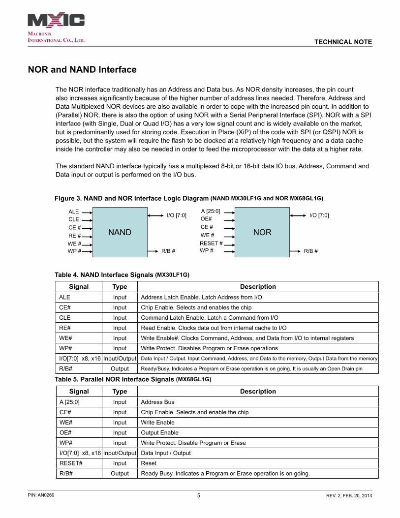
NOR and NAND Interface
The NOR interface traditionally has an Address and Data bus. As NOR density increases, the pin count also increases significantly because of the higher number of address lines needed. Therefore, Address and Data Multiplexed NOR devices are also available in order to cope with the increased pin count. In addition to (Parallel) NOR, there is also the option of using NOR with a Serial Peripheral Interface (SPI). NOR with a SPI interface (with Single, Dual or Quad I/O) has a very low signal count and is widely available on the market, but is predominantly used for storing code. Execution in Place (XiP) of the code with SPI (or QSPI) NOR is possible, but the system will require the flash to be clocked at a relatively high frequency and a data cache inside the controller may also be needed in order to feed the microprocessor with the data at a higher rate.
The standard NAND interface typically has a multiplexed 8-bit or 16-bit data IO bus. Address, Command and Data input or output is performed on the I/O bus.
Figure 3. NAND and NOR Interface Logic Diagram (NAND MX30LF1G and NOR MX68GL1G)
NOR
A [25:0]OE#CE #WE #RESET #WP #
I/O [7:0]
R/B #
NAND
ALECLECE #RE #WE #WP #
I/O [7:0]
R/B #
Table 4. NAND Interface Signals (MX30LF1G)
Table 5. Parallel NOR Interface Signals (MX68GL1G)
Signal Type DescriptionALE Input Address Latch Enable. Latch Address from I/O
CE# Input Chip Enable. Selects and enables the chip
CLE Input Command Latch Enable. Latch a Command from I/O
RE# Input Read Enable. Clocks data out from internal cache to I/O
WE# Input Write Enable#. Clocks Command, Address, and Data from I/O to internal registers
WP# Input Write Protect. Disables Program or Erase operations
I/O[7:0] x8, x16 Input/Output Data Input / Output. Input Command, Address, and Data to the memory, Output Data from the memory
R/B# Output Ready/Busy. Indicates a Program or Erase operation is on going. It is usually an Open Drain pin
Signal Type DescriptionA [25:0] Input Address Bus
CE# Input Chip Enable. Selects and enable the chip
WE# Input Write Enable
OE# Input Output Enable
WP# Input Write Protect. Disable Program or Erase
I/O[7:0] x8, x16 Input/Output Data Input / Output
RESET# Input Reset
R/B# Output Ready Busy. Indicates a Program or Erase operation is on going.
6P/N: AN0269 REV. 2, FEB. 20, 2014
TECHNICAL NOTE
"Table 6. Signal Pin Count for NAND and NOR Interfaces (1Gb)" compares the signal pin count of a 1Gb NAND device with a Parallel Page mode 1Gb NOR . With such a big memory size, the address lines required cause the pin count to increase significantly for the NOR. To make the comparison complete, a solution employing two serial NOR devices (so as to achieve an 8 bit I/O data bus width) is also shown.
Table 6. Signal Pin Count for NAND and NOR Interfaces (1Gb)
NAND NOR (Parallel) 2 x NOR (QSPI)IO [7:0] A[26:0] 2 x IO[3:0]
CE# IO[7:0] CLK
RE# CE# 2 x CE#
WE# OE#
CLE WE#
ALE RESET#
WP# WP#
R/B#
Pin Count: 15 Pin Count: 40 Pin Count: 11
Read and Program Operations
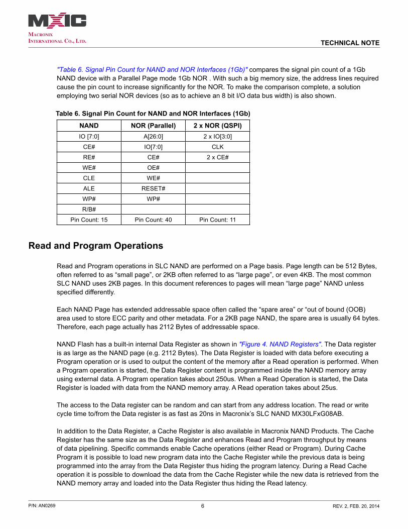
Read and Program operations in SLC NAND are performed on a Page basis. Page length can be 512 Bytes, often referred to as “small page”, or 2KB often referred to as “large page”, or even 4KB. The most common SLC NAND uses 2KB pages. In this document references to pages will mean “large page” NAND unless specified differently.
Each NAND Page has extended addressable space often called the “spare area” or “out of bound (OOB) area used to store ECC parity and other metadata. For a 2KB page NAND, the spare area is usually 64 bytes. Therefore, each page actually has 2112 Bytes of addressable space.
NAND Flash has a built-in internal Data Register as shown in "Figure 4. NAND Registers". The Data register is as large as the NAND page (e.g. 2112 Bytes). The Data Register is loaded with data before executing a Program operation or is used to output the content of the memory after a Read operation is performed. When a Program operation is started, the Data Register content is programmed inside the NAND memory array using external data. A Program operation takes about 250us. When a Read Operation is started, the Data Register is loaded with data from the NAND memory array. A Read operation takes about 25us.
The access to the Data register can be random and can start from any address location. The read or write cycle time to/from the Data register is as fast as 20ns in Macronix’s SLC NAND MX30LFxG08AB.
In addition to the Data Register, a Cache Register is also available in Macronix NAND Products. The Cache Register has the same size as the Data Register and enhances Read and Program throughput by means of data pipelining. Specific commands enable Cache operations (either Read or Program). During Cache Program it is possible to load new program data into the Cache Register while the previous data is being programmed into the array from the Data Register thus hiding the program latency. During a Read Cache operation it is possible to download the data from the Cache Register while the new data is retrieved from the NAND memory array and loaded into the Data Register thus hiding the Read latency.
7P/N: AN0269 REV. 2, FEB. 20, 2014
TECHNICAL NOTE
Figure 4. NAND Registers
Data register
Cache register
blockpage
Array
HOSTData in
Program
Data out
Read
20 ns / Byte or Word
250 us / page
20 ns / Byte or Word
25 us / page
Data register
Cache register
blockpage
Array
HOSTData in
Program
Data out
Read
20 ns / Byte or Word
250 us / page
20 ns / Byte or Word
25 us / page
NOR Flash also uses Registers to output the data, but the size of the buffer is very small (e.g. 16 to 32 Bytes) compared to NAND. However the Read register can be loaded with a very short latency (e.g. 100 ns). A Write Buffer Register is also available in order to optimize the programming throughput in NOR, but the size is also very small (e.g. 64 to 256 Bytes) compared to NAND. The reason for smaller sized NOR registers is due to the different Read and Programming methods used by the two technologies.
Software
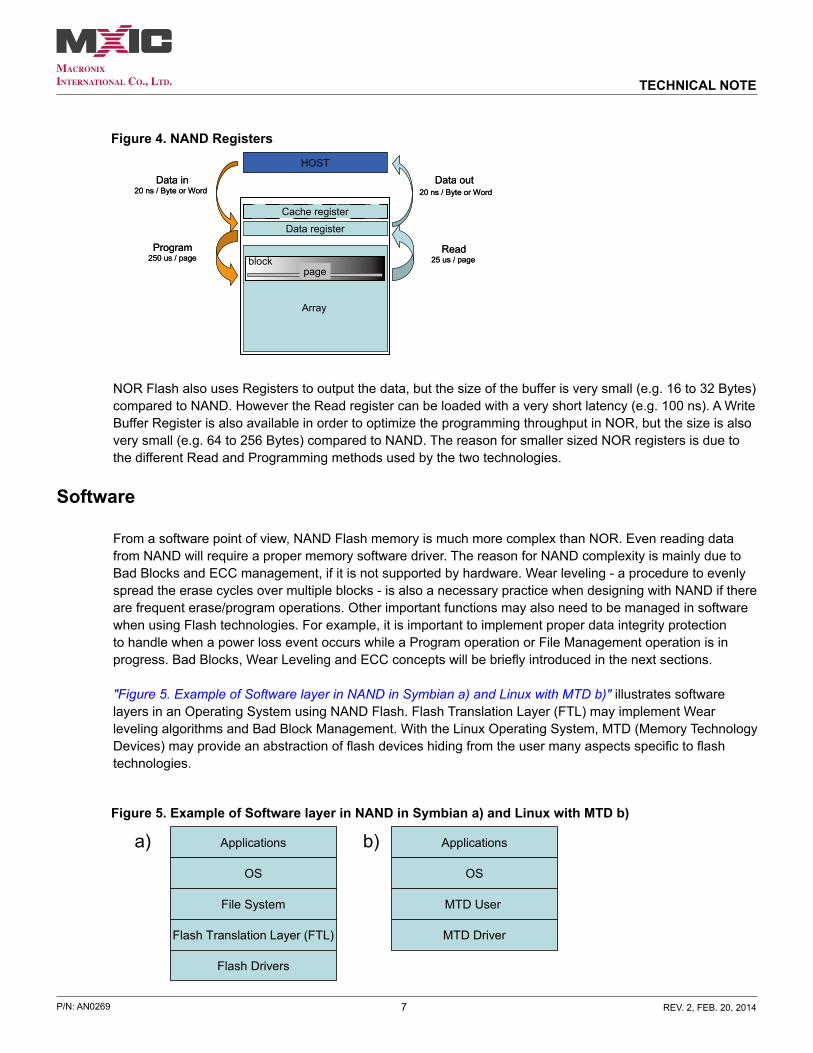
From a software point of view, NAND Flash memory is much more complex than NOR. Even reading data from NAND will require a proper memory software driver. The reason for NAND complexity is mainly due to Bad Blocks and ECC management, if it is not supported by hardware. Wear leveling - a procedure to evenly spread the erase cycles over multiple blocks - is also a necessary practice when designing with NAND if there are frequent erase/program operations. Other important functions may also need to be managed in software when using Flash technologies. For example, it is important to implement proper data integrity protection to handle when a power loss event occurs while a Program operation or File Management operation is in progress. Bad Blocks, Wear Leveling and ECC concepts will be briefly introduced in the next sections.
"Figure 5. Example of Software layer in NAND in Symbian a) and Linux with MTD b)" illustrates software layers in an Operating System using NAND Flash. Flash Translation Layer (FTL) may implement Wear leveling algorithms and Bad Block Management. With the Linux Operating System, MTD (Memory Technology Devices) may provide an abstraction of flash devices hiding from the user many aspects specific to flash technologies.
Figure 5. Example of Software layer in NAND in Symbian a) and Linux with MTD b)
Applications
OS
File System
Flash Translation Layer (FTL)
Flash Drivers
Applications
OS
MTD User
MTD Driver
a) b)
8P/N: AN0269 REV. 2, FEB. 20, 2014
TECHNICAL NOTE
Error Correction Codes (ECC)
NAND requires Error Correction Code in order to obtain reliable operation. ECC algorithms commonly implemented are Hamming for 1-bit correction and BCH for more than 1-bit correction. It is a common practice to refer the correction capability as the error bit number that can be corrected over a 512B chunk of data even if the real implementation operates on larger data blocks. The ECC algorithms can be implemented either in software or in hardware by the NAND controller. Very often the NAND memory controller in the host has the built-in ECC correction capability and must be configured to match properly with the NAND type used in the system.
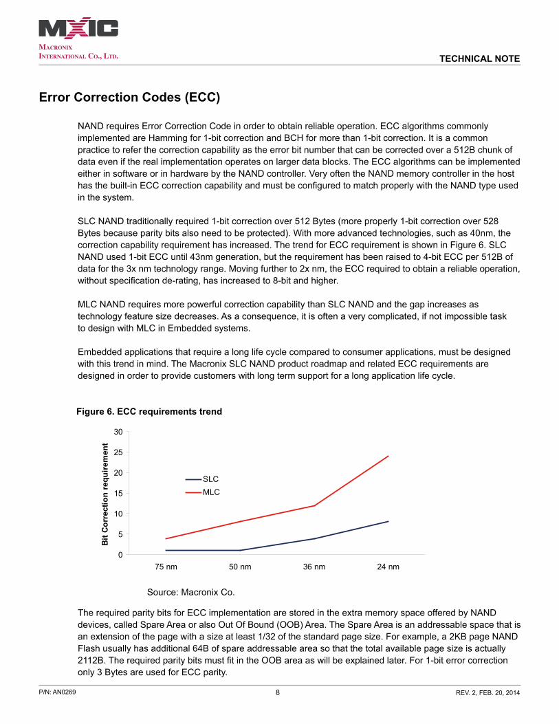
SLC NAND traditionally required 1-bit correction over 512 Bytes (more properly 1-bit correction over 528 Bytes because parity bits also need to be protected). With more advanced technologies, such as 40nm, the correction capability requirement has increased. The trend for ECC requirement is shown in Figure 6. SLC NAND used 1-bit ECC until 43nm generation, but the requirement has been raised to 4-bit ECC per 512B of data for the 3x nm technology range. Moving further to 2x nm, the ECC required to obtain a reliable operation, without specification de-rating, has increased to 8-bit and higher.
MLC NAND requires more powerful correction capability than SLC NAND and the gap increases as technology feature size decreases. As a consequence, it is often a very complicated, if not impossible task to design with MLC in Embedded systems.
Embedded applications that require a long life cycle compared to consumer applications, must be designed with this trend in mind. The Macronix SLC NAND product roadmap and related ECC requirements are designed in order to provide customers with long term support for a long application life cycle.
Figure 6. ECC requirements trend
0
5
10
15
20
25
30
75 nm 50 nm 36 nm 24 nm
Bit C
orre
ctio
n re
quire
men
t
SLCMLC
Source: Macronix Co.
The required parity bits for ECC implementation are stored in the extra memory space offered by NAND devices, called Spare Area or also Out Of Bound (OOB) Area. The Spare Area is an addressable space that is an extension of the page with a size at least 1/32 of the standard page size. For example, a 2KB page NAND Flash usually has additional 64B of spare addressable area so that the total available page size is actually 2112B. The required parity bits must fit in the OOB area as will be explained later. For 1-bit error correction only 3 Bytes are used for ECC parity.
9P/N: AN0269 REV. 2, FEB. 20, 2014
TECHNICAL NOTE
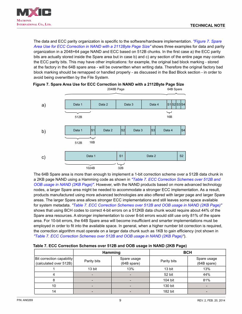
The data and ECC parity organization is specific to the software/hardware implementation. "Figure 7. Spare Area Use for ECC Correction in NAND with a 2112Byte Page Size" shows three examples for data and parity organization in a 2048+64 page NAND and ECC based on 512B chunks. In the first case a) the ECC parity bits are actually stored inside the Spare area but in case b) and c) any section of the entire page may contain the ECC parity bits. This may have other implications: for example, the original bad block marking - stored at the factory in the 64B spare area - will be overwritten when writing data. Therefore the original factory bad block marking should be remapped or handled properly - as discussed in the Bad Block section - in order to avoid being overwritten by the File System.
Figure 7. Spare Area Use for ECC Correction in NAND with a 2112Byte Page Size
The 64B Spare area is more than enough to implement a 1-bit correction scheme over a 512B data chunk in a 2KB page NAND using a Hamming code as shown in "Table 7. ECC Correction Schemes over 512B and OOB usage in NAND (2KB Page)". However, with the NAND products based on more advanced technology nodes, a larger Spare area might be needed to accommodate a stronger ECC implementation. As a result, products manufactured using more advanced technologies are also offered with larger page and larger Spare areas. The larger Spare area allows stronger ECC implementations and still leaves some space available for system metadata. "Table 7. ECC Correction Schemes over 512B and OOB usage in NAND (2KB Page)" shows that using BCH codes to correct 4-bit errors on a 512KB data chunk would require about 44% of the Spare area resources. A stronger implementation to cover 8-bit errors would still use only 81% of the spare area. For 10-bit errors, the 64B Spare area will become insufficient and smarter implementations must be employed in order to fit into the available space. In general, when a higher number bit correction is required, the correction algorithm must operate on a larger data chunk such as 1KB to gain efficiency (not shown in "Table 7. ECC Correction Schemes over 512B and OOB usage in NAND (2KB Page)").
Table 7. ECC Correction Schemes over 512B and OOB usage in NAND (2KB Page)
Data 1 Data 2 Data 3 Data 4 S1 S2 S3 S4
512B 16B
2048B Page 64B Spare
Data 1 Data 2 Data 3 Data 4S1 S2 S3 S4
512B 16B
a)
b)
Data 1 S1
1024B 32B
c) Data 2 S2
Hamming BCHBit correction capability (calculated over 512B)
Parity bitsSpare usage (64B spare)
Parity bits Spare usage (64B spare)
1 13 bit 13% 13 bit 13%4 - - 52 bit 44%8 - - 104 bit 81%
10 - - 130 bit -14 - - 182 bit -
10P/N: AN0269 REV. 2, FEB. 20, 2014
TECHNICAL NOTE
Due to routine data management in NAND Flash (wear leveling, garbage collection), sometimes data is moved to a fresh block while a particular block is being erased and cleaned up. When data copy is done, it is necessary to recalculate the ECC and eventually correct the data before writing back to the new block to avoid any errors being accumulated. Data management operations are performed by the controller or the system software layer.
Macronix focuses on long term support of its SLC NAND Flash families. ECC free NAND solutions are also available. This strategy allows the controller chip and system makers sufficient time to update their product lines independently of frequent changes in the mainstream NAND market.
Bad Blocks
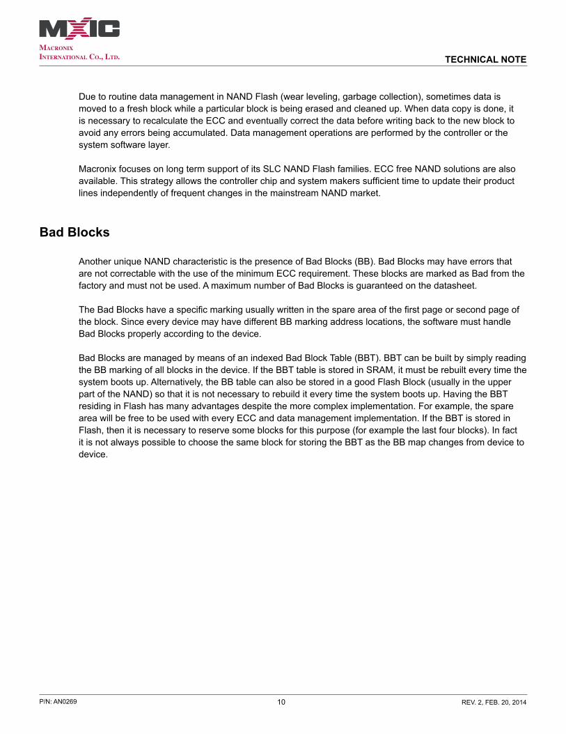
Another unique NAND characteristic is the presence of Bad Blocks (BB). Bad Blocks may have errors that are not correctable with the use of the minimum ECC requirement. These blocks are marked as Bad from the factory and must not be used. A maximum number of Bad Blocks is guaranteed on the datasheet.
The Bad Blocks have a specific marking usually written in the spare area of the first page or second page of the block. Since every device may have different BB marking address locations, the software must handle Bad Blocks properly according to the device.
Bad Blocks are managed by means of an indexed Bad Block Table (BBT). BBT can be built by simply reading the BB marking of all blocks in the device. If the BBT table is stored in SRAM, it must be rebuilt every time the system boots up. Alternatively, the BB table can also be stored in a good Flash Block (usually in the upper part of the NAND) so that it is not necessary to rebuild it every time the system boots up. Having the BBT residing in Flash has many advantages despite the more complex implementation. For example, the spare area will be free to be used with every ECC and data management implementation. If the BBT is stored in Flash, then it is necessary to reserve some blocks for this purpose (for example the last four blocks). In fact it is not always possible to choose the same block for storing the BBT as the BB map changes from device to device.
11P/N: AN0269 REV. 2, FEB. 20, 2014
TECHNICAL NOTE
Every time a BB is addressed, the proper software layer (depending on the SW implementation) will use the BBT to redirect the access to a good block. Each time a Block fails in the application, the Block may be retired and marked as Bad. The Bad Block table will be updated accordingly.
The BBT must be stored in a good block and the SW handling Bad Blocks must be able to find the BBT location every time it boots up. NAND Flash Blocks can wear out and so can the Block where the BBT is stored. Therefore the BBT must be moved to a different good Block.
Figure 8. Bad Block Table Indexing
start
Block 0
CheckBB mark
Last block?
Mark BB Next block
end
fail
no
Wear Leveling
Wear Leveling is a technique that extends the life cycle of a NAND memory device used for data storage. There is a limitation on the number of program/erase cycles for each block in a NAND flash. In addition, a highly cycled block will see its reliability reduced in terms of data retention. If certain data locations are written more frequently than others, then the blocks involved will be cycled more than average, and eventually wear out. The purpose of wear leveling is to remap the data blocks in order to average out the number of cycles for every block in the device.
Wear leveling consists of remapping the Logical Block Address (LBA) from the host into the Physical Block Address (PBA) of a Flash device. The Software or the NAND controller will store a Remap Table that redirects the LBA from the host to PBA as shown in example of Figure 9.
Wear leveling can be implemented either in a very simple form or in more advanced forms. The choice for the type of wear leveling depends on the application. Two common methods of implementing wear leveling are Static Wear leveling or Dynamic Wear leveling.

12P/N: AN0269 REV. 2, FEB. 20, 2014
TECHNICAL NOTE
In Code storage applications, most of the memory contains code that is seldom updated: we refer to this type of data as Static. Only a small section of the NAND device might be used for storing files, parameters or data and we will refer it as Dynamic data.
In Dynamic Wear leveling when a block needs to be updated, the new data is written into a free block with the lowest erase count and the Map Table is updated accordingly. The block containing the older block can be erased and made free for new data. In this scenario it might happen that some data that is not updated will remain in the same block for a long time.
In Static Wear leveling, the purpose is to keep the Program/Erase count uniform among all the blocks. Referring to the previous example, even if data does not need to be updated, it might be moved to another block in order to achieve a uniform cycle count over all blocks. The pure Static Wear Leveling approach might also move Code data - that in principle does not need to be moved - in order to average the cycle count over the entire NAND Flash. For this reason software architects may decide to apply Static Wear Leveling only to a portion of the addressing space.
Static Wear leveling is much more complex to handle than Dynamic Wear leveling but it allows us to achieve the maximum endurance. However, not all the applications may require Static Wear Leveling. The best choice depends on the Static data and Dynamic data characteristics and requirements.
Figure 9. Wear leveling Block Remapping
CONTROLLER / SWBlock Remapping Table
……2103
50n
12210100
PBALBA
……2103
50n
12210100
PBALBA
HOSTaddress
MEMORYaddress
13P/N: AN0269 REV. 2, FEB. 20, 2014
TECHNICAL NOTE
Boot from NAND
SLC NAND normally guarantees that Block 0 is free of errors so that the system can always boot from this area. However, when booting from NAND, the software might need to consider bad blocks if the boot code is too large for Block 0 to accommodate.
Macronix NAND SLC Flash guarantees the validity of Block 0. This means that applications can always boot from Block 0. In some Macronix NAND products, a lower ECC strength is required for Block 0 compared to other blocks because the Block0 is guaranteed to be cycled few times. However, it is suggested that, if possible, the strongest ECC be implemented on Block 0 when booting so that Block 0 will be treated as any other good block.
Macronix NAND also implements a Block 0 auto load feature. The first page of Block 0 is automatically loaded into the Cache Registers at power-on and can be directly loaded without the need of addressing it first.
Because NAND is not directly executable, it is necessary to load a first stage boot to a SRAM/DRAM for execution. The controller has to identify the NAND type before executing the boot-loading code. If the controller has a fixed boot-loading sequence (hard coded or in ROM), it is important that the future NAND products are backward compatible with all aspects related to boot-loading.
Some application/controllers will boot without ECC correction on the NAND data. Macronix NAND is tested to guarantee the maximum reliability, but in this case, however, it is suggested to use the maximum ECC correction to guarantee error-free operation.
Conclusion
NAND Flash memory is becoming the memory of choice in embedded systems and code storage applications. This document introduces NAND Flash memory and discusses the advantages of its use in embedded applications. A comparison with NOR Flash memory is also provided.
Revision HistoryRevision No. Description Page Date
REV. 1 Initial Release ALL 12th, Dec., 2013
REV. 2 Content modification P.1, 3, 12 20th, Feb., 2014
14P/N: AN0269 REV. 2, FEB. 20, 2014
TECHNICAL NOTE
MACRONIX INTERNATIONAL CO., LTD. reserves the right to change product and specifications without notice.
Except for customized products which have been expressly identified in the applicable agreement, Macronix's products are designed, developed, and/or manufactured for ordinary business, industrial, personal, and/or household applica-tions only, and not for use in any applications which may, directly or indirectly, cause death, personal injury, or severe property damages. In the event Macronix products are used in contradicted to their target usage above, the buyer shall take any and all actions to ensure said Macronix's product qualified for its actual use in accordance with the applicable laws and regulations; and Macronix as well as it’s suppliers and/or distributors shall be released from any and all liabil-ity arisen therefrom.
Copyright© Macronix International Co., Ltd. 2013~2014. All rights reserved, including the trademarks and tradename thereof, such as Macronix, MXIC, MXIC Logo, MX Logo, Integrated Solutions Provider, NBit, Nbit, NBiit, Macronix NBit, eLiteFlash, HybridNVM, HybridFlash, XtraROM, Phines, KH Logo, BE-SONOS, KSMC, Kingtech, MXSMIO, Macro-nix vEE, Macronix MAP, Rich Au dio, Rich Book, Rich TV, and FitCAM. The names and brands of third party referred thereto (if any) are for identification purposes only.
For the contact and order information, please visit Macronix’s Web site at: http://www.macronix.com