hdd to 3d-nand and beyond_oct2016_satoruaraki
TRANSCRIPT

HDD TO FLASH & BEYOND- TECHNOLOGY / CARRIER CHALLENGES -
OCT 18, 2016
SATORU ARAKI
10/18/2016@ 2016 Satoru Araki, all right reserved 1

HDD TO FLASH & BEYOND – EXECUTIVE SUMMARY
ØPOSITIONING IN NEXT NEW TECHNOLOGY WAVES• Data Storage is one of the Key Module in IoT Big Waves, as well as Sensor,
Wireless, Software, and AI• FLASH has Promising Future in Huge Volume Expansion, because of 3D
Capacity Scalability & Cost Reduction• However, Storage-Class Memory is emerging to cover DRAM and FLASH area
ØFLASH MEMORY CHALLENGES• 3D NAND Continuous Scalability Expansion: >100 by 2020, >500 Layer by
2030 per ITRS2015• Cost and Performance
ØEMERGING STORAGE CLASS MEMORY CHALLENGES• Current Candidates: 3D XPoint, ReRAM, MRAM, FeRAM• Cost, Scalability, Performance• Vertical Structure Integration
10/18/2016@ 2016 Satoru Araki, all right reserved 2

AGENDA
Ø RECENT FORECAST/FACT STATEMENT
Ø IOT - POSITIONING IN NEXT NEW TECHNOLOGY WAVES
Ø DATA STORAGE HIERARCHY
Ø FLASH MEMORY BASICS
Ø 3D NAND TECHNOLOGY
Ø COMPETITIVE LANDSCAPE
Ø BEYOND 3D NAND – NON VOLATILE MEMORY
10/18/2016@ 2016 Satoru Araki, all right reserved 3

RECENT FORECAST/FACT STATEMENTS
Ø IoT – 50 Billion Devices will be connected to the network Ø IoT Market Scale – $45B in 2020Ø FLASH Memory Market Scale – $31B in 2015Ø Data Generation – 44 Zeta Bytes in 2020Ø Recent Merge & Acquisition Info & Rumors
• Qualcomm -> NXP, $30B • Softbank -> ARM, $33B• Renesas -> Intersil, $3B• WD -> SanDisk, $15B
10/18/2016@ 2016 Satoru Araki, all right reserved 4
IoT Market
Data Generation
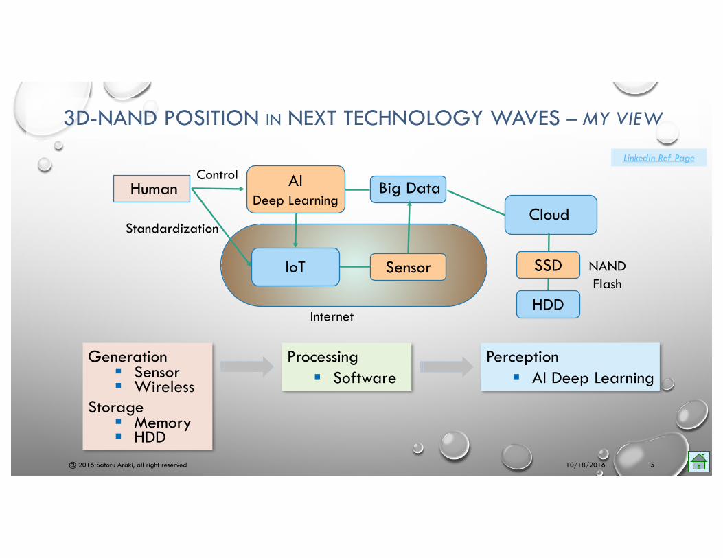
3D-NAND POSITION IN NEXT TECHNOLOGY WAVES – MY VIEW
10/18/2016@ 2016 Satoru Araki, all right reserved 5
Big DataAIDeep Learning
CloudHuman
Internet
NAND Flash
Standardization
Control
IoT Sensor SSD
HDD
LinkedIn Ref Page
Generation§ Sensor§ Wireless
Storage§ Memory§ HDD
Processing§ Software
Perception§ AI Deep Learning

DATA STORAGE HIERARCHY
10/18/2016@ 2016 Satoru Araki, all right reserved 6
§ FLASH Memory Replaces Performance and Consumer HDD § DRAM on Top of the Hierarchy – Very Expensive§ Persistent (Storage Class) Memory – Emerging to Invade DRAM
Flash Memory
Performance HDD
Consumer HDD
Ref. 1

DATA STORAGE MEMORY HIERARCHY – HDD TO FLASH
10/18/2016@ 2016 Satoru Araki, all right reserved 7
§ Storage-Class Memory Emerging to Cover DRAM Space§ New Non-Volatile Memory – ReRAM, Phase Change, MRAM
Ref. 2

FLASH MEMORY BASICS
§ Modification from MOS-FET, by Inserting Floating Gate • Injecting Electrons into Floating Gate by Tunneling Effect
§ Multi-Level bits by Controlling Electrons in FG
10/18/2016@ 2016 Satoru Araki, all right reserved 8
Gate
SiO2
Gate: 0 V Gate: +
Source (N)
Drain (N)P-type
+-Gate
SiO2Source
(N)Drain
(N)P-type
+-+
N
MOS-FET
PN
+-
CG
++ FG ++
Gate: 0 V Gate: +
Source (N)
Drain (N)
P-type
+-CG
- FG -Source
(N)Drain
(N)P-type
+-+
FLASH
N
Vgate
Vgate
VTH
Dis
VTH
Dis“1” “0”
VTH
“Multi”
4 bit (QLC) – 16 level3 bit (TLC) – 8 level2 bit (MLC) – 4 level1 bit (SLC) – 2 level

WHY 3D-NAND ?
10/18/2016@ 2016 Satoru Araki, all right reserved 9
§ 3D Multilayer Structure Enables Higher Bit Density/area
Charge Trap(SONOS)
SiO2Si9N10SiO2
Poly-Si
source drain
CG
90degflip
SiO2Poly-Si
Si9N10
SiO2 Poly-Si
1
2
3
N-1
N
V-Channel(3D)
. . .
. . .
Functional Layers by Vertical Wall Deposition
Ref. 2
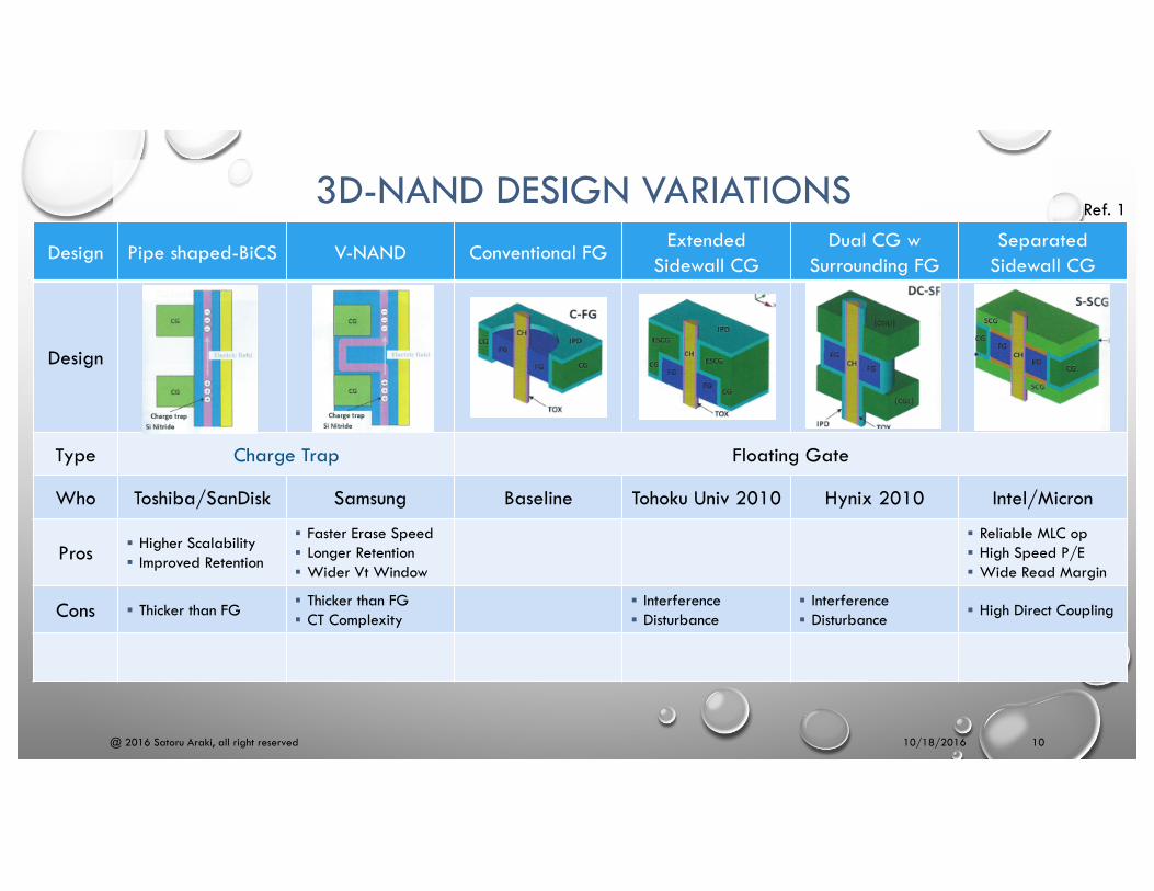
3D-NAND DESIGN VARIATIONS
10/18/2016@ 2016 Satoru Araki, all right reserved 10
Design Pipe shaped-BiCS V-NAND Conventional FGExtended
Sidewall CGDual CG w
Surrounding FGSeparated
Sidewall CG
Design
Type Charge Trap Floating Gate
Who Toshiba/SanDisk Samsung Baseline Tohoku Univ 2010 Hynix 2010 Intel/Micron
Pros § Higher Scalability§ Improved Retention
§ Faster Erase Speed§ Longer Retention§ Wider Vt Window
§ Reliable MLC op§ High Speed P/E§ Wide Read Margin
Cons § Thicker than FG § Thicker than FG§ CT Complexity
§ Interference§ Disturbance
§ Interference§ Disturbance § High Direct Coupling
Ref. 1
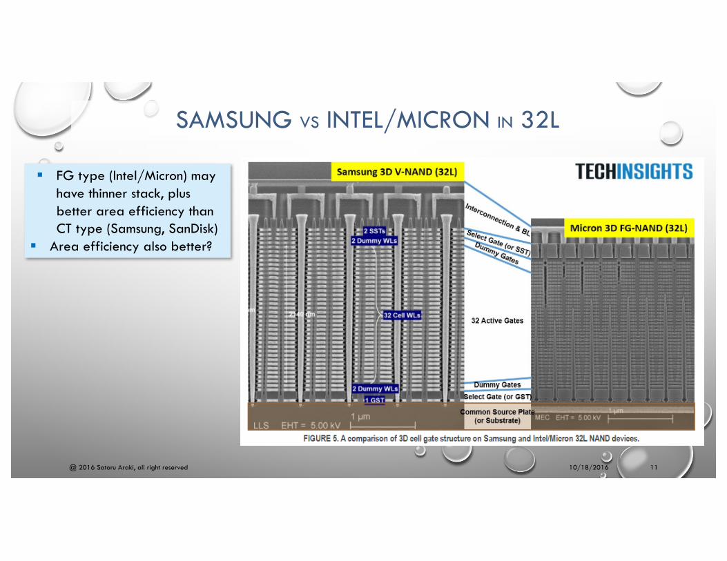
SAMSUNG VS INTEL/MICRON IN 32L
10/18/2016@ 2016 Satoru Araki, all right reserved 11
§ FG type (Intel/Micron) may have thinner stack, plus better area efficiency than CT type (Samsung, SanDisk)
§ Area efficiency also better?

FLASH PROCESS ROADMAP– COMPETITION
10/18/2016@ 2016 Satoru Araki, all right reserved 12
§ Samsung leads the competition as 3D volume production from 2014
§ Toshiba/SanDisk follows§ Intel/Micron comes up with
new 3D Xpoint in 2016. Production unknown

3D-NAND POSITIONING IN MEMORY TREND – ITRS2015
10/18/2016@ 2016 Satoru Araki, all right reserved 13
§ Official Roadmap shows 100 Layers in 2020, and continuously increase >500 Layers in 2030
§ Max Bit may stay in TLC – 3 bit

EMERGING STORAGE CLASS MEMORY – BEYOND FLASH
10/18/2016@ 2016 Satoru Araki, all right reserved 14
§ Storage-Class Memory – New Category to Cover Both DRAM & FLASH§ Non-Volatile§ Several Candidates as of now: 3D XPoint, ReRAM, MRAM, FeRAM, etc
Storage-Class Memory
Ref. 1
Key Requirements:§ Cost§ Scalability§ Performance

3D XPOINT BY INTEL/MICRON
10/18/2016@ 2016 Satoru Araki, all right reserved 15
§ 3D XPoint is a ReRAM with Phase Change Material?
Ref. 6

Resistive RAM – NON VOLATILE MEMORY
10/18/2016@ 2016 Satoru Araki, all right reserved 16
§ Pros: ü Simple Device Structureü Faster R/W Speed
§ Consü Critical Layer Patterningü New Material Development
Ref. 1
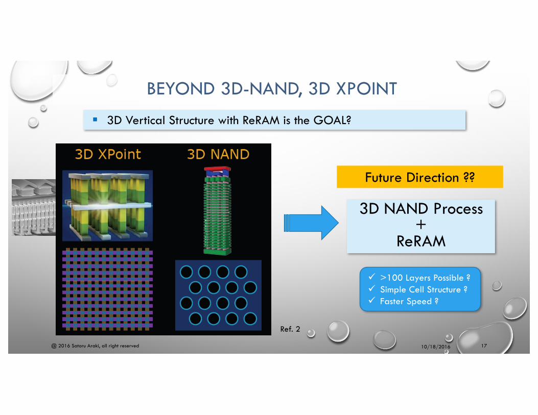
BEYOND 3D-NAND, 3D XPOINT
10/18/2016@ 2016 Satoru Araki, all right reserved 17
§ 3D Vertical Structure with ReRAM is the GOAL?
3D NAND Process+
ReRAM
Future Direction ??
ü >100 Layers Possible ?ü Simple Cell Structure ?ü Faster Speed ?
Ref. 2

MKW VENTURES AT FLASH MEMORY SUMMIT 2016
10/18/2016@ 2016 Satoru Araki, all right reserved 18Ref. 5

3D-ReRAM – SanDisk View
10/18/2016@ 2016 Satoru Araki, all right reserved 19
§ 3D Multilayer Structure Enables Higher Bit Density/area
Ref. 2

TECHNOLOGY & CARRIER CHALLENGES – WHAT CAN WE BRING?
10/18/2016@ 2016 Satoru Araki, all right reserved 20
Challenges§ Semiconductor Device Experience§ Device Know-how§ Product Kow-how
Transferrable Skills§ Tunnel Barrier Knowhow§ Thin Film Deposition, Etching Knowhow§ Reliability Methodology
Challenges§ No track record in Semi§ No direct leadership experience§ Proven Certificate – PMP, PgMP, CSM§ Experience in Semi, part timer?
Transferrable Carrier§ Engineering Management Skills§ Leadership Traits§ Project, Prog, Prod Management Skills
TECHNOLOGY CARRIER
REFERENCES
1. “3D FLASH MEMORIES”, Ed. Rino Micheloni, Springer ISBN 978-94-017-8510-6
2. Siva Sivaram, Keynote-4: Creating Storage Class Memory: Learning from 3D NAND Flash Memory Summit 2016, Link
3. ITRS2015 Executive Summary, Link
4. TECHINSIGHTS, NAND Flash Memory Roadmap, Link
5. Mark Webb, MKW Ventures, Flash Memory Summit 2016, Link
6. Seshubabu Desu, 4DS Memory Limited, Flash Memory Summit 2016, Link
7. Jim Handy, Objective Analysis, Flash Memory Summit 2016, Link
8. Forbes, Roundup Of Internet of Things Forecasts And Market Estimates, 2015, Link
9. Gartner, Press Release, Processing, Sensing and Communications Semiconductor Device Portion of the IoT Is Set for Rapid Growth, Link
10. ATKearney, Big Data and the Creative Destruction of Today's Business Models, Link
10/18/2016@ 2016 Satoru Araki, all right reserved 21

Visual Management Board
2/09/2017@ 2017 Satoru Araki, all right reserved 22
Near-Term Action Item Responsible Team Member Due Date Completion
DateM / S / C Priority Comments
Create prototype parts kit Jane M. 4/27/09 M Parts missing
Draft test plan out for review Joe P. 5/1/09 5/8/09 S Complete
Complete circuit simulation Cedrick M. 5/1/09 M Need Resources!!
Order injection-mold tooling Joline Q. 5/5/09 M
Meet with key supplier Harry P. 5/10/09 C
Prepare for customer meeting Dave N. 5/10/09 S
Key Milestone Responsible Team Member
Planned Completion
Date
Actual Completion
Date
Cost Status
Schedule Status
Tech. Status Comments
Fabricate Prototype David Copperfield 6/7/09 6/7/09 Complete
Prototype Testing Oliver Twist 4/5/09 First Test Failed
Prototype Validated Tiny Tim 3/14/09 May Require Rework
Production Tooling Charles Darney 4/24/09 Supplier Issues
Test Plan Complete Sydney Carton 4/20/09 Resources Unavailable
Final Drawing Release Lucy Mannette 5/17/09
Fabricate Qual Units Charles Dickens 6/14/2009
Planned Work Project Timeline
Unplanned Work
Parking Lot
Week 1 Week 2Mon Wed Fri Mon Wed Fri
Out
Out Out
Out
Tom
Dick
Harry
Jane
Sally
Mary
Two-Week Action Plan
Risk Management
0
5
10
15
20
25
Months from Project Start
Proj
ect “
Risk
Rat
ing”

BACK UP
10/18/2016@ 2016 Satoru Araki, all right reserved 23

3D-NANDFlash- ChallengesandCompetitiveLandscape-
JULY8,2016
SATORUARAKI
7/08/2016 @2016SatoruAraki,allrightreserved 24

3DFlashChallenges– ExecutiveSummary§ PositioninginNextNewTechnologyWaves◦ Promisinginvolumehugeexpansion,but3Dcapacityscalability&costarecrucial
§ ProcessChallenges◦ Reducingprocessvariationinetchedholedepthprofileandsize◦ Tunnelingbarrierandchargetraplayermaterialandprocessoptimization
§ DeviceChallenges◦ DesignoptimizationforVthreshold shiftandreliabilityimprovement◦ Designscalability>100layers
§ TunnelingBarrierChallenges◦ Opportunitytoimprovedesignmarginbynewmaterials
§ CompetitiveLandscape◦ Samsungaheadin256Gb(3D48-layerTLC)– mainbattlefieldin2016/2017
§ NextActionsinProductEngineering
7/08/2016 @2016SatoruAraki,allrightreserved 25

3D-NANDPositioninNextTechnologyWaves– myview
BigDataAIDeepLearning
CloudHuman
Internet
NANDFlash
Standardization
Control
IoT Sensor SSD
HDD
7/08/2016 @2016SatoruAraki,allrightreserved 26
LinkedInRefPage
3D-NANDhasPromisingFutureif;§ Keepcapacityscalabilitywith§ Costcompetitiveness,Reliability

3DProcessChallenges§ V-ConnectionThroughHoleEtchingUniformity◦ HighAspectRatio,48à 64,80layerextendibility,variationminimization◦ Holesize,depthprofile,wallroughness,etc
§ TunnelingBarrierUniformityforHoleWall◦ Keyfilminterfacequalityimprovement◦ ALDdepositionvariationminimizationinholedepth◦ RestrictionofthebarriermaterialforALD
§ ChargeTrapLayerMaterialandProperties◦ Materialselectionandprocessoptimization
§ LongerThroughput,LowerYieldby48à 64,80Layer§ HigherHoleDensityduetoDepositionCoveragetotheWall§ Poly-SiFilmQualityImprovement§ ControlGateLeadFabricationProcessComplexityin48à 64,80Layer
7/08/2016 @2016SatoruAraki,allrightreserved 27
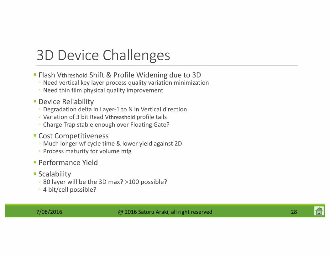
3DDeviceChallenges§ FlashVthreshold Shift&ProfileWideningdueto3D◦ Needverticalkeylayerprocessqualityvariationminimization◦ Needthinfilmphysicalqualityimprovement
§ DeviceReliability◦ DegradationdeltainLayer-1toNinVerticaldirection◦ Variationof3bitReadVthreashold profiletails◦ ChargeTrapstableenoughoverFloatingGate?
§ CostCompetitiveness◦ Muchlongerwf cycletime&loweryieldagainst2D◦ Processmaturityforvolumemfg
§ PerformanceYield§ Scalability◦ 80layerwillbethe3Dmax?>100possible?◦ 4bit/cellpossible?
7/08/2016 @2016SatoruAraki,allrightreserved 28

TunnelingBarrierChallenges§ BarrierDepositionProcessUniformity◦ ToptobottombarrierSiO2 thicknessvariation à S/N,reliability,yieldissue◦ Etchingholediameter/depthprofileuniformity à Vvariation,reliability,yieldissue
§MaterialImprovement◦ Manynewmaterialsbeingproposedbutmaynotsuitablefor3D:Gd2TiO5,Gd2O3,ZrO2,HfO2,etc◦ Restrictionfordepositingtodeepaspectratioholes◦ Potentialtoimproveitbymetal-CVD+oxidation ß TMRlessonsinHDD
7/08/2016 @2016SatoruAraki,allrightreserved 29
Poly-Si
SiO2 SiO2Si9N10SiO2
Poly-Si
FloatingGate(FG)
ChargeTrap(SONOS)
source drain source drain
CG
CGSiO2Poly-Si
Si9N10SiO2 Poly-Si
1
2
3
N-1
N
90degflip
V-Channel(3D)
...
...
Type Merit
FG SiO2 controlSONOS SiO2/SiN/SiO2/p-Si Faster prog/erase
High-k Al2O3, La2O3, ZrO2, HfO2, Gd2TiO5
Faster Prog/erase speed
MOHOS SiO2/Gd2TiO5/SiO2/p-Si Faster programming/erase Larger memory window
TunnelingBarrier

CompetitiveLandscape§ 3DImplementation◦ 256Gbit chipproductionisthemainbattlefield◦ Samsungwillstartshippingin2016◦ Toshiba/SanDisk2016/E,announcedFab2inv andconstruction,3Dratio50%2017,80%2018
§ CapacityChampionData◦ Samsung:◦ Micron: 768GbTLC,3Dw/FGatISSCCFeb,2016
§ CellDesignperDepositionStepsin256Gb◦ Samsung96,Toshiba/SanDisk144,Micron128- why?
§ EmergingTech:ReRAM,MRAM,etc
7/08/2016 @2016SatoruAraki,allrightreserved 30
J.Choe,FlashMemorySummit2015,Comparisonof2x/1xnm2DPlanarand3DV-NANDArchitecture
§ 2DProduction◦ 75-80%Node15nminallSamsung,Toshiba/SanDisk,Micron/Intel,SKHynix
◦ PlannedNode9nmin2018

§ 256Gbisthemainbattlefield◦ Samsungalreadyinproduction◦ Toshiba/SanDiskisabouttostartproductionthisyear◦ Micron/Intel,SKHynixbehind– catchingupaggressively
7/08/2016 @2016SatoruAraki,allrightreserved 31
Gen Date Capacity 3D-Tech CellDepo Process Status Production Volume Investment Spec
1st Aug/2013 128GbMLC 24layers 20nm2nd May/2014 128GbMLC/TLC 32layersV-NAND 20nm inProduction
3rd Dec/2016 256GbTLC 48layersV-NAND 96depo 15/16nm Sampling PM971-NVMe,512GB/p 540/520MB/sr/w,98k/90kr/eIOPS
1st2nd Apr/2016 128GbMLC/TLC 32layersBiCS
3rd Dec/2016 256GbTLC 48layersBiCS 144depo 15/16nm Sampling3Dproductionwillstartat2016/E.Fab2constwillstart3/2017
2015:0,2016:start,2017:50%,2018:80%
$8Bfromeach,$15Btotalto2018fiscal/E
2015:0,2016:start,2017:50%,2018:80%
64GbMLC 25nm3rd 2016 256/386Gb,MLC/TLC 32layers 128depo2nd 3Q/2015 128GbMLC 36layers3rd 2016 48layers
Samsung
Micron/Intel
Toshiba/SanDisk
SKHynix
CompetitiveLandscape– cont’d

3DProductEngineering- NextActions§ 3DNANDProductLaunch– 1st Priority
§ DeeperCollaboration:MilpitasDesign/Eng’g TeamandJapanWf FabTeam◦ Utilizeandfuseeachteam’sculturalstrength◦ Needacoordinatorasa“ConnectionPin”.How?– hereisareflink.Let’sdiscussitlater
§ CompetitiveBenchmarkingforDesign/ProcessFeedback
§Manymore…..Let’sdiscussthemlateron…
7/08/2016 @2016SatoruAraki,allrightreserved 32