improving quantum hardware: building new superconducting
TRANSCRIPT
Improving Quantum Hardware: Building
New Superconducting Qubits and
Couplers
Thomas Michael Hazard
A Dissertation
Presented to the Faculty
of Princeton University
in Candidacy for the Degree
of Doctor of Philosophy
Recommended for Acceptance
by the Department of
Physics
Adviser: Professor Andrew A. Houck
June 2019

© Copyright by Thomas Michael Hazard, 2019.
All rights reserved.
Abstract
Over the past 10 years, improvements to the fundamental components in supercon-
ducting qubits and the realization of novel circuit topologies have increased the life-
times of qubits and catapulted this architecture to become one of the leading hardware
platforms for universal quantum computation. Despite the progress that has been
made in increasing the lifetime of the charge qubit by almost six orders of magnitude,
further improvements must be made to climb over the threshold for fault tolerant
quantum computation. Two complementary approaches towards achieving this goal
are investigating and improving upon existing qubit designs, and looking for new
types of superconducting qubits which would offer some intrinsic improvements over
existing designs. This thesis will explore both of these directions through a detailed
study of new materials, circuit designs, and coupling schemes for superconducting
qubits. In the first experiment, we explore the use of disordered superconducting
films, specifically Niobium Titanium Nitride, as the inductive element in a fluxonium
qubit and measure the loss mechanisms limiting the qubit lifetime. In the second
experiment, we work towards the experimental realization of the 0 − π qubit archi-
tecture, which offers the promise of intrinsic protection in lifetime and decoherence
compared to existing superconducting qubits. In the final experiment, we design and
measure a two qubit device where the static σz ⊗ σz crosstalk between the two qubits
is eliminated via destructive interference. The use of multiple coupling elements re-
moves the σz ⊗ σz crosstalk while maintaining the large σz ⊗ σx interaction needed to
perform two qubit gates.
i

Acknowledgements
This thesis wouldn’t have been possible without the support of my family, friends,
coworkers and mentors. While I cannot list everyone here, I must say that during the
process of writing this thesis, I have thought of you and I would like to thank you all!
First, I must thank my advisor Professor Andrew Houck. Andrew’s guidance
and support has been instrumental in helping me grow as scientist and person. His
ability to get to the core of any problem quickly and simultaneously maintain a broad
perspective is unmatched by any other scientist I have ever met. If it weren’t for
the no cloning theorem and there were 20 copies of Andrew, we would have built
a 1000 qubit quantum computer years ago. His scientific advice has always been
complemented with a cheerful sense of humor and a reminder to not take myself too
seriously. I am immeasurably grateful for all the advice he has given me and for
everything he has done for me during my PhD.
To the all the Houck lab members, grad school can be a long journey but you have
made it a fun one. Andras Gyenis and Pranav Mundada, working with you both has
been a pleasure and I have always been impressed by your ability to calmly be able to
work through so many challenges that arise in the long hours of fab and measurement.
Thank you both for the many hours of scientifically stimulating conversations and
explanations, and for the late night climbing sessions at the rock wall. Alicia Kollar
has been tremendously helpful in providing scientific ideas and perspective as well as
giving great feedback on the thesis! Andrei Vrajitoarea and Zhaoqi Leng have been
a wonderful scientific sounding board for random ideas and very useful discussions.
Anjali Premkumar, Alex Place, Basil Smitham and Jake Bryon have been helpful
with their enthusiasm and questions, best of luck to you all as you continue your
paths in grad school and beyond! Mattias Fitzpatrick, our Monday morning chats
about philosophy, physics and life have been a great way to start every week. Your
friendship in and out of the lab has been an amazing part of my time at Princeton.iv

To those friends who have already graduated, Gengyan Zhang, Neereja Sundare-
san, Srikanth Srinivasan, Jiri Stehlik, Sorawis (Peace) Sangtawesin, Loren Alegria,
and Xiao Mi thank you for the mentorship and guidance when I was young student.
Dave Zajac, thank you for the introduction to rock climbing. Those three hour drives
up to the Gunks were a great time to learn about climbing and physics from you.
To the friends in my cohort year, especially Peter Brown, Yonglong Xie, Kevin
Crowley, Tong Gao, and Jun Yi Lee, it seems like yesterday that we were all panicked
about prelims and courses, but now somehow have made it and are moving on to
bigger and better things! Thank you to so many other friends for your kind words and
interesting conversations including Felix, Kasey, Prashanth, Justin, Sonia, Matteo,
Kenan, Lauren, Zach, and Abe. Thank you to all people past and present on the
Physics softball team and Professors Page and Verlinde for your support, it has been
an honor to captain the Big Bangers for so many summers, good luck this season.
Thank you to all the Physics and Engineering support staff who play such a
big part in every student’s success during their PhD, including Kate Brosowksy,
Barbara Fruhling, Steve Lowe, Ted Lewis, Julio Lopez and Darryl Johnson. Darryl,
in particular has been one of the kindest and most professional people I have ever
met. If the university gave out an MVP award for staff members, he would take the
title every year. Thank you to Professor Bakr as well for reading this thesis. Thank
you Professor Petta for the opportunity to work in your lab on spin qubits.
To all my friends and family away from Princeton, it was hard to move far away
for so long, but your love and support have really helped. Especially from my sister
Jenna!
To Mallika, grad school can be tough at times, but going through it with someone
else has made the journey incredible. Your love, understanding, and patience through
the all the late nights in lab and cleanroom has been wonderful. You truly are an
amazing person, friend, and scientist.
v

And finally to Mom and Dad, your love and support know no bound. You have
always been there to encourage me in all my hobbies and interests, and have been
fantastic role models. Since I started talking and asking questions, you have helped
foster my creativity about the world and have shaped the person I am today. I
couldn’t have done it without you.
vi

To my family.
vii

Contents
Abstract . . . . . . . . . . . . . . . . . . . . . . . . . . . . . . . . . . . . . iii
Acknowledgements . . . . . . . . . . . . . . . . . . . . . . . . . . . . . . . iv
List of Figures . . . . . . . . . . . . . . . . . . . . . . . . . . . . . . . . . . xii
List of Tables . . . . . . . . . . . . . . . . . . . . . . . . . . . . . . . . . . xiv
1 Introduction 1
1.1 Quantum computing with qubits . . . . . . . . . . . . . . . . . . . . 2
1.2 Thesis overview . . . . . . . . . . . . . . . . . . . . . . . . . . . . . . 3
2 Theoretical background 4
2.1 Josephson Junctions . . . . . . . . . . . . . . . . . . . . . . . . . . . 4
2.2 Circuit Quantization . . . . . . . . . . . . . . . . . . . . . . . . . . . 6
2.3 Types of superconducting qubits . . . . . . . . . . . . . . . . . . . . . 9
2.3.1 Cooper pair box . . . . . . . . . . . . . . . . . . . . . . . . . . 9
2.3.2 Transmon . . . . . . . . . . . . . . . . . . . . . . . . . . . . . 11
2.3.3 Flux qubit . . . . . . . . . . . . . . . . . . . . . . . . . . . . . 12
2.3.4 Fluxonium . . . . . . . . . . . . . . . . . . . . . . . . . . . . . 13
2.3.5 The 0− π qubit . . . . . . . . . . . . . . . . . . . . . . . . . . 17
2.4 Qubit-resonator coupling . . . . . . . . . . . . . . . . . . . . . . . . . 25
2.5 Relaxation in qubits . . . . . . . . . . . . . . . . . . . . . . . . . . . 27
2.6 Kinetic Inductance . . . . . . . . . . . . . . . . . . . . . . . . . . . . 29
viii
CONTENTS
3 Experimental Techniques 31
3.1 Fabrication . . . . . . . . . . . . . . . . . . . . . . . . . . . . . . . . 31
3.1.1 Junction types . . . . . . . . . . . . . . . . . . . . . . . . . . 33
3.1.2 Junction resistance . . . . . . . . . . . . . . . . . . . . . . . . 33
3.2 Packaging and shielding . . . . . . . . . . . . . . . . . . . . . . . . . 35
3.3 Measurement setup . . . . . . . . . . . . . . . . . . . . . . . . . . . . 36
3.3.1 Dilution Refrigerator . . . . . . . . . . . . . . . . . . . . . . . 36
3.3.2 Wiring . . . . . . . . . . . . . . . . . . . . . . . . . . . . . . . 36
3.4 Microwave measurement techniques . . . . . . . . . . . . . . . . . . . 39
3.4.1 Microwave networks . . . . . . . . . . . . . . . . . . . . . . . 40
3.4.2 CPW resonators . . . . . . . . . . . . . . . . . . . . . . . . . 43
3.4.3 Microwave spectroscopy . . . . . . . . . . . . . . . . . . . . . 47
3.4.4 Pulsed measurements . . . . . . . . . . . . . . . . . . . . . . . 48
3.5 Characterization of NbTiN films . . . . . . . . . . . . . . . . . . . . . 49
3.5.1 Sheet resistance and Tc . . . . . . . . . . . . . . . . . . . . . . 49
3.5.2 Resonators . . . . . . . . . . . . . . . . . . . . . . . . . . . . . 50
4 Nanowire Superinductance Fluxonium Qubit 53
4.1 Device design . . . . . . . . . . . . . . . . . . . . . . . . . . . . . . . 54
4.2 Spectrum measurement . . . . . . . . . . . . . . . . . . . . . . . . . . 56
4.3 Multilevel spectroscopy . . . . . . . . . . . . . . . . . . . . . . . . . . 60
4.4 Lifetime spectroscopy . . . . . . . . . . . . . . . . . . . . . . . . . . . 64
5 Protected qubits: The 0−π circuit 67
5.1 0− π readout coupling . . . . . . . . . . . . . . . . . . . . . . . . . . 67
5.2 Soft 0−π regime . . . . . . . . . . . . . . . . . . . . . . . . . . . . . . 69
5.3 Fabrication . . . . . . . . . . . . . . . . . . . . . . . . . . . . . . . . 70
ix
CONTENTS
5.4 Spectroscopy . . . . . . . . . . . . . . . . . . . . . . . . . . . . . . . 72
5.5 0−π lifetime measurements . . . . . . . . . . . . . . . . . . . . . . . . 73
6 Elimination of Static Crosstalk 76
6.1 ZZ crosstalk . . . . . . . . . . . . . . . . . . . . . . . . . . . . . . . . 77
6.2 Improved device design . . . . . . . . . . . . . . . . . . . . . . . . . . 79
6.2.1 Device fabrication . . . . . . . . . . . . . . . . . . . . . . . . . 81
6.2.2 Spectrum characterization . . . . . . . . . . . . . . . . . . . . 82
6.3 ZZ crosstalk map . . . . . . . . . . . . . . . . . . . . . . . . . . . . . 84
6.4 Single qubit gate tuneup . . . . . . . . . . . . . . . . . . . . . . . . . 84
6.5 Single qubit randomized benchmarking . . . . . . . . . . . . . . . . . 86
6.6 iSWAP gate . . . . . . . . . . . . . . . . . . . . . . . . . . . . . . . . 87
6.6.1 Quantum state tomography . . . . . . . . . . . . . . . . . . . 89
6.7 Cross-resonance gate . . . . . . . . . . . . . . . . . . . . . . . . . . . 92
7 Conclusion and Outlook 95
A Fabrication Recipes 98
A.1 NSFQ and nanowire 0− π process flow . . . . . . . . . . . . . . . . . 98
A.2 Zero ZZ process flow . . . . . . . . . . . . . . . . . . . . . . . . . . . 98
A.3 Niobium preparation . . . . . . . . . . . . . . . . . . . . . . . . . . . 99
A.4 Photolithography . . . . . . . . . . . . . . . . . . . . . . . . . . . . . 101
A.5 Niobium etching . . . . . . . . . . . . . . . . . . . . . . . . . . . . . . 102
A.6 Electron beam lithography . . . . . . . . . . . . . . . . . . . . . . . . 102
A.7 Aluminum evaporation . . . . . . . . . . . . . . . . . . . . . . . . . . 104
B Electrostatic simulations for design of zero ZZ device 107
x

CONTENTS
C Publications and Presentations 109
Bibliography 110
xi

List of Figures
2.1 LC oscillator . . . . . . . . . . . . . . . . . . . . . . . . . . . . . . . . 7
2.2 The Cooper pair box . . . . . . . . . . . . . . . . . . . . . . . . . . . 10
2.3 Transmon Energy levels and Wavefunctions . . . . . . . . . . . . . . 12
2.4 Spectrum of the flux qubit . . . . . . . . . . . . . . . . . . . . . . . . 13
2.5 Fluxonium circuit . . . . . . . . . . . . . . . . . . . . . . . . . . . . . 14
2.6 Fluxonium energies and wavefunctions . . . . . . . . . . . . . . . . . 15
2.7 Heavy fluxonium energies and wavefunctions . . . . . . . . . . . . . . 18
2.8 The 0− π circuit . . . . . . . . . . . . . . . . . . . . . . . . . . . . . 19
2.9 0− π circuit modes . . . . . . . . . . . . . . . . . . . . . . . . . . . . 21
2.10 0− π effective potential . . . . . . . . . . . . . . . . . . . . . . . . . 23
2.11 0− π spectrum and wavefunctions . . . . . . . . . . . . . . . . . . . . 24
2.12 Relaxation model . . . . . . . . . . . . . . . . . . . . . . . . . . . . . 27
2.13 Kinetic Inductance . . . . . . . . . . . . . . . . . . . . . . . . . . . . 29
3.1 Junction Types . . . . . . . . . . . . . . . . . . . . . . . . . . . . . . 34
3.2 Fridge wiring schematic . . . . . . . . . . . . . . . . . . . . . . . . . . 39
3.3 CPW resonators . . . . . . . . . . . . . . . . . . . . . . . . . . . . . . 46
3.4 Network analyzer setup . . . . . . . . . . . . . . . . . . . . . . . . . . 47
3.5 Pulsed measurement block diagram . . . . . . . . . . . . . . . . . . . 48
3.6 NbTiN test wire resistances . . . . . . . . . . . . . . . . . . . . . . . 50
xii

LIST OF FIGURES
3.7 NbTiN resonators . . . . . . . . . . . . . . . . . . . . . . . . . . . . . 51
4.1 NSFQ circuit diagram and image . . . . . . . . . . . . . . . . . . . . 55
4.2 NSFQ two tone spectroscopy . . . . . . . . . . . . . . . . . . . . . . . 57
4.3 Autler-Townes splitting . . . . . . . . . . . . . . . . . . . . . . . . . . 62
4.4 T1 spectroscopy . . . . . . . . . . . . . . . . . . . . . . . . . . . . . . 65
5.1 Capacitively coupled 0− π circuit . . . . . . . . . . . . . . . . . . . . 68
5.2 0− π circuit layout . . . . . . . . . . . . . . . . . . . . . . . . . . . . 69
5.3 Soft 0− π spectrum . . . . . . . . . . . . . . . . . . . . . . . . . . . . 71
5.4 Soft 0− π wavefunctions . . . . . . . . . . . . . . . . . . . . . . . . . 73
5.5 Measured 0− π energy spectrum . . . . . . . . . . . . . . . . . . . . 74
5.6 0− π relaxation measurements . . . . . . . . . . . . . . . . . . . . . . 75
6.1 Theoretical ZZ and ZX strenghts . . . . . . . . . . . . . . . . . . . . 82
6.2 Zero ZZ device image . . . . . . . . . . . . . . . . . . . . . . . . . . . 83
6.3 Zero ZZ two-tone spectroscopy . . . . . . . . . . . . . . . . . . . . . . 83
6.4 Cross-Ramsey ζ map . . . . . . . . . . . . . . . . . . . . . . . . . . . 85
6.5 AllXY measurements . . . . . . . . . . . . . . . . . . . . . . . . . . . 86
6.6 Randomized Benchmarking . . . . . . . . . . . . . . . . . . . . . . . 88
6.7 iSWAP interaction . . . . . . . . . . . . . . . . . . . . . . . . . . . . 89
6.8 Single shot readout corrected SWAP oscillations . . . . . . . . . . . . 91
6.9 Quantum state tomography . . . . . . . . . . . . . . . . . . . . . . . 93
6.10 CR oscillations . . . . . . . . . . . . . . . . . . . . . . . . . . . . . . 94
B.1 Zero ZZ Maxwell simulation . . . . . . . . . . . . . . . . . . . . . . . 108
xiii

List of Tables
3.1 Junction resistances . . . . . . . . . . . . . . . . . . . . . . . . . . . . 35
3.2 Attenuation configuration comparison . . . . . . . . . . . . . . . . . . 38
3.3 CPW parameters . . . . . . . . . . . . . . . . . . . . . . . . . . . . . 51
4.1 NSFQ Two-mode fit parameters . . . . . . . . . . . . . . . . . . . . . 59
4.2 NSFQ Single mode approximation parameters . . . . . . . . . . . . . 60
6.1 Zero ZZ device parameters . . . . . . . . . . . . . . . . . . . . . . . . 81
B.1 Capacitance matrix . . . . . . . . . . . . . . . . . . . . . . . . . . . . 107
xiv

Chapter 1
Introduction
As originally conceived [1], quantum computers would be most useful for problems
physicists are interested in. It can be argued that the study of very small scale
quantum “processors” in the past 30 years has led to a deeper understanding of these
systems themselves rather than performing complex calculations. One generality of
quantum systems is that they are extremely fragile, in particular, two level quantum
bits, or qubits, face an underlying tension between isolation and control. Qubits can
be made nearly isolated from the universe and can have very long lifetimes, but this
makes it impossible to control them in a deterministic way in order to perform useful
computations. Modern “Quantum Mechanics and Engineers” continue to improve
how qubits are constructed, using better materials and removing extraneous couplings
to the environment. A large portion of these efforts involve improving qubit energy
relaxation time, T1. Relaxation times in state of the art superconducting qubits
pose a significant challenge for near term quantum computation. Assuming gate
operations and state preparation can be made perfect, a rough approximation for
the maximum number of qubit gates can be expressed as 1/T1. With current T1
values of ∼ 100 µs in superconducting qubits and two qubit gate times of ∼ 100 ns,
without error correction, this puts an upper limit of about 103 gates before all useful
1

CHAPTER 1. INTRODUCTION
information about the system will be lost. Therefore, understanding and mitigating
the sources of relaxation in qubits is an active topic of research [2, 3]. Even if no
further advances to qubit lifetimes or gate speeds are made, the implementation of
error correcting surface codes [4] could allow for the operation of a fault tolerant
quantum computer. Although these codes allow for errors at the present level, there
is a cost to be paid in that the number of physical qubits to construct a single logical
qubit is on the order of 104 and that a vast majority of the gate operations and
computation time would be spent correcting faulty qubits. With that in mind, we
take the approach of improving existing qubits and coupling between qubits as a
means towards the realization of a fault-tolerant quantum computer.
1.1 Quantum computing with qubits
A qubit is the quantum analog of a classical bit, that is, a two state quantum system
that can be in an arbitrary superposition of the two states. A quantum computer [5],
will likely contain a physical qubit layer consisting of qubits, controls and readout
circuitry, as well as a logical layer containing a “quantum compiler” and controller
to run algorithms [6]. The DiVincenzo criteria lay out a set of general guidelines
for the construction of a quantum computer, namely, the underlying system should
be comprised of physically “scalable” qubits, all the qubits need to be initialized in
a known state, the decoherence and relaxation times in the system must be “long”,
there must be a universal set of quantum gates, and the qubits must be able to be
measured with high fidelity [7]. It is interesting to note that two of the criteria, the
system scalability and coherence times, are particularly vague and continue to be
redefined as new hardware and error correcting schemes are realized. Based on these
five criteria, the last two decades have seen an incredible amount of advancement
2
CHAPTER 1. INTRODUCTION
in different physical implementations of qubits and small-scale quantum computers,
including superconducting qubits [8, 9], quantum dots [10, 11], bulk NMR systems
[12, 13], photonic systems [14, 15], ultracold atoms [16, 17], and trapped ions [18, 19].
Among these physical systems, superconducting qubits have emerged as one of
the most promising candidates in constructing a gate-based quantum computer. The
building blocks of superconducting circuits include inductors, capacitors, and Joseph-
son junctions (JJs). With this small set of circuit elements, the field of circuit Quan-
tum Electrodynamics (cQED) has expanded and explored a wide variety of qubits
with different properties. In particular, the transmon [20], essentially a slightly an-
harmonic oscillator, has emerged as the most ubiquitous superconducting qubit, due
to its simple level structure, long coherence, and ease of manufacture [21]. Despite
these properties, the transmon might not be the qubit in a final quantum computer
if its coherence and lifetime cannot continue to be improved. Making improvements
to transmons and looking for “life after the transmon” are two topics explored in this
work.
1.2 Thesis overview
The work in this thesis is presented as follows. Chapter 2 presents a brief overview
of superconducting qubits. Chapter 3 describes the experimental methods and setup
used for measuring superconducting devices. Chapter 4 details our work in measuring
a fluxonium qubit with an inductive element formed by a thin nanowire of NbTiN.
Chapter 5 explores experiments on a protected 0−π qubit. In Chapter 6, we describe
a two qubit, two coupler scheme to eliminate static crosstalk between qubits. A brief
summary and outlook of the thesis is presented in Chapter 7, and several additional
detailed discussions can be found in the Appendices.
3
Chapter 2
Theoretical background
In this section, we consider some of the building blocks of superconducting qubits.
We describe the method of circuit quantization which allows us to understand the
eigenmodes of general quantum circuits. We discuss several types of superconducting
qubits as well as their distinguishing characteristics. The framework for qubit coupling
and relaxation is introduced. We conclude with a description of kinetic inductance.
2.1 Josephson Junctions
If two superconductors are placed into contact with a thin insulating layer be-
tween, a Josephson Junction (JJ) is formed. This type of junction is known as a
superconductor-insulator-superconductor (S-I-S) junction in which the insulating
layer between the two superconductors needs to be thin enough to allow Cooper
pairs to tunnel between the superconductors. In what is known as the first Josephson
relation [22], a zero-voltage current, I, will flow across the junction, and is given by
I = Ic sinϕ, (2.1)
4
CHAPTER 2. THEORETICAL BACKGROUND
where ϕ is the difference in phase of the Ginzburg-Landau wavefunction between
the two superconductors and Ic is the critical current of the junction [22, 23]. The
second Josephson relation states that if a voltage difference V is maintained across
the junction, the time evolution of the phase difference across the junction is given
by:d (∆ϕ)dt
= 2eV~. (2.2)
The energy stored in a JJ can be obtained by integrating the electrical work done by
a current source in changing the phase across the junction:
∫IsV dt =
∫Is(~/2e)d(∆ϕ)→ const.− EJ cos (∆ϕ) , (2.3)
where EJ ≡ ~Ic/2e. Ic can be related to the normal state resistance of the JJ through
the Ambegaokar-Baratoff relation [24]
IcRn = π∆2e tanh
(∆
2kBT
), (2.4)
where ∆ is the energy gap of the superconductor at T = 0 K. Each JJ will have
an additional charging energy, which can be thought to arise from the capacitance
between the two superconducting leads, and is given by ECJ = e2/2CJ where e
is the electron charge and CJ is the capacitance between the leads. The JJ has
two properties that make it desirable for constructing qubits, first, its intrinsic non-
linearity from the sinusoidal current relation, and second, the junction itself is free
of dissipation. These features will allow us to construct circuits with a wide range of
properties from simple arrangements of JJs, linear inductors and capacitors.
5

CHAPTER 2. THEORETICAL BACKGROUND
2.2 Circuit Quantization
One of the most powerful theoretical tools at our disposal is circuit quantization [25–
27]. This allows us to take macroscopic objects with many degrees of freedom and
reduce the collective behavior into a small number of parameters that characterize
the circuit. Our goal is to obtain the circuit Hamiltonian and its corresponding
eigenenergies based on a small number of input parameters (capacitance in the circuit,
Josephson energy, etc.). To that end, we begin by defining a magnetic flux variable,
Φ,
Φ (t) =∫ t
−∞V (τ) dτ (2.5)
as the time integral of the voltage, V across a circuit element, as well as the charge
Q,
Q (t) =∫ t
−∞I (τ) dτ (2.6)
as the time integral of the current flowing through a circuit element. Let’s now
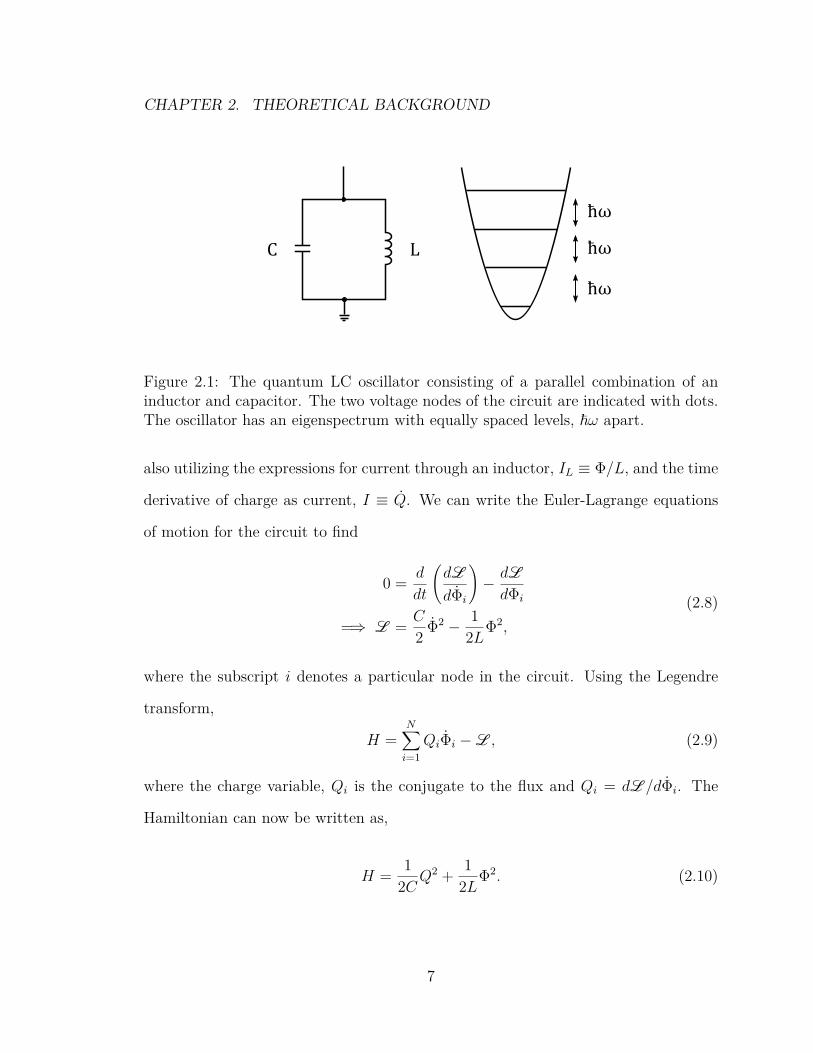
consider a simple LC oscillator consisting of an inductor, with inductance L, placed
in parallel with a capacitor, with capacitance C (Figure 2.1). We can define the two
voltage nodes on either side of the inductor, and make use of gauge invariance to set
the potential at one of the nodes to ground. This leaves the circuit with one degree
of freedom (dof). To generalize, a circuit with n voltage nodes will be left with n− 1
dof’s. We make use of Kirchoff’s law that the sum of currents into and out of a node
must be equal,
IL + IC = 0 = ΦL
+ Q
0 = ΦL
+ CΦ,(2.7)
6
CHAPTER 2. THEORETICAL BACKGROUND
C L ħω
ħω
ħω
Figure 2.1: The quantum LC oscillator consisting of a parallel combination of aninductor and capacitor. The two voltage nodes of the circuit are indicated with dots.The oscillator has an eigenspectrum with equally spaced levels, ~ω apart.
also utilizing the expressions for current through an inductor, IL ≡ Φ/L, and the time
derivative of charge as current, I ≡ Q. We can write the Euler-Lagrange equations
of motion for the circuit to find
0 = d
dt
(dL
dΦi
)− dL
dΦi
=⇒ L = C
2 Φ2 − 12LΦ2,
(2.8)
where the subscript i denotes a particular node in the circuit. Using the Legendre
transform,
H =N∑i=1
QiΦi −L, (2.9)
where the charge variable, Qi is the conjugate to the flux and Qi = dL/dΦi. The
Hamiltonian can now be written as,
H = 12CQ
2 + 12LΦ2. (2.10)
7

CHAPTER 2. THEORETICAL BACKGROUND
One additional definition that can be made for convenience is the impedance of the
oscillator, Z0 ≡√L/C. We can now quantize the circuit by introducing the creation
and annihilation operators, defined as
a =∞∑0
√n+ 1|n〉〈n+ 1| (2.11)
a† =∞∑0
√n+ 1|n+ 1〉〈n|, (2.12)
where the states |n〉 are the harmonic oscillator eigenstates and the commutation
relation between a and a† is given by[a, a†
]=1, and write the phase and charge
variables as operators to find
Q =√
~2Z0
i(a† − a
)Φ =
√~Z0
2(a† + a
), (2.13)
which results in a Hamiltonian of the form
H = ~ωr(a†a+ 1/2
), (2.14)
where ωr = 1/√LC. It will become useful to draw the analogy between the electrical
and mechanical harmonic oscillators, where the capacitive energy is equivalent to the
kinetic energy of the oscillator and the inductive energy is equivalent to the potential
energy. A harmonic oscillator by itself makes a poor qubit due to the equal spacing
between the Fock states [28] and so generally, the linear inductor is replaced with a
non-linear JJ, allowing the Hilbert space to be truncated to the first two levels of the
system, from which we can make a qubit.
8

CHAPTER 2. THEORETICAL BACKGROUND
2.3 Types of superconducting qubits
As the number of degrees of freedom in superconducting circuits is small, they are
often treated as “artificial atoms”. Unlike true atomic systems, artificial supercon-
ducting atoms have no fundamental characteristic which uniquely identifies its type.
The superconducting qubit community has historically applied different names to cir-
cuits with varying levels of differences between them. Broadly speaking, most qubits
to date have two voltage nodes and consist of a Josephson junction, or pair of junc-
tions in a SQUID loop, where the two sides of the junction are either capacitively or
inductively shunted. Most of the different types of qubits come from different limits
of Josephson energy EJ , the charging energy EC , and inductive energy EL. Here we
will provide a brief, and by no means exhaustive, list of superconducting circuits and
their salient features.
2.3.1 Cooper pair box
A Cooper pair box (CPB) [29–31] consists of a single (or two) junctions(s) with a
small capacitance between the superconducting leads. The Hamiltonian is given by
H = 4EC (n− ng)2 − EJ cos ϕ, (2.15)
where n is the integer number of excess Cooper pairs across the JJ, ng is the di-
mensionless offset charge between the islands, the charging energy EC = e2/2C, and
EJ/EC is typically of order unity. The voltage on a nearby gate electrode is used to
tune ng. A diagram of two styles of CPB along with the energy spectra for EJ/EC = 1
and EJ/EC = 5 are shown in Figure 2.2. The charge dispersion, εm = dEm/dng, for
a CPB is large away from integer and half integer values of ng, making it extremely
9
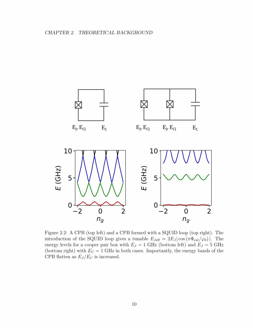
CHAPTER 2. THEORETICAL BACKGROUND
EJ, ECJ EC EJ, ECJ ECEJ, ECJ
2 0 2ng
0
5
10
E (G
Hz)
2 0 2ng
0
5
10E
(GHz
)
Figure 2.2: A CPB (top left) and a CPB formed with a SQUID loop (top right). Theintroduction of the SQUID loop gives a tunable EJeff = 2EJ | cos (πΦext/ϕ0) |. Theenergy levels for a cooper pair box with EJ = 1 GHz (bottom left) and EJ = 5 GHz(bottom right) with EC = 1 GHz in both cases. Importantly, the energy bands of theCPB flatten as EJ/EC is increased.
10

CHAPTER 2. THEORETICAL BACKGROUND
susceptible to charge noise, and even when operated at charge sweet spots (ng values
where dEm/dng = 0), the coherence times of the CPB typically are less that 1 µs.
2.3.2 Transmon
A transmon [20, 32] is a CPB in the limit that EJ/EC 1. Using the analogy of EC
as inverse mass, the transmon is a “heavy” CPB. In the transmon regime, the charge
dispersion of the the mth energy level can be expressed as,
εm ' EC24m+5
m!
√2π
(EJ
2EC
)m2 + 3
4e−√
8EJ/EC (2.16)
which leads to an exponential suppression of charge noise sensitivity as the ratio of
EJ/EC is increased. In this regime, the qubit frequency is given by,
~ω01 '√
8EJEC − EC (2.17)
The difference between the 0→1 and 1→2 transition frequencies, or anharmonicity, is
defined as α ≡ ω12−ω01 ' EC , with typical transmons having α values between -200
to -400 MHz, which makes the transmon a weakly anharmonic oscillator. The size of
α is important as it sets a “speed limit” on the controlling gates, that is to say, short
gate lengths will have larger high frequency Fourier components causing excitations
of higher qubit levels. Figure 2.3 shows the energy levels and wavefunctions for
a transmon with EJ/EC=50. Although the CPB/transmon has made tremendous
improvements in coherence and lifetimes in the last 20 years [33, 34], we can see
that the phase matrix element between the ground and excited states will always
be of order unity, given that the wavefunctions are highly overlapping, which has
implications for the ultimate limit of T1 as discussed in Section 2.5.
11

CHAPTER 2. THEORETICAL BACKGROUND
2 0 2ng
0
10
20E
(GHz
)
1 0 10
10
20
30
E (G
Hz)
Figure 2.3: The spectrum (left) of the transmon, qubit vs. ng for EJ = 15 GHz, andEC = 0.3 GHZ. The charge dispersion has been reduced to ε1 = 2.2 kHz, makingthe qubit nearly immune to charge noise. The square of the first few wavefunctionsplotted in the cosine Josephson potential (right).
2.3.3 Flux qubit
A flux qubit [35] consists of a single junction shunted by two or more smaller junctions.
Although there is no strict definition for the number of shunting junctions, flux qubits
are usually fabricated with less than 2-5, and the value of d, a unit-less area scale
factor, is picked such that EL ∼ EJ . The phase difference across the large junctions is
much smaller than the single small junction, and therefore the shunting junctions can
be treated as a single linear inductor, which adds an additional term to the circuit
Hamiltonian, EL which will be the inverse sum of the EJ/d’s,
H = 4EC n2 − EJ cos ϕ+ 12EL
(ϕ+ 2πΦext
ϕ0
)2
. (2.18)
The ng has been removed through the dc shunt across the junction [36], which makes
the qubit insensitive to charge fluctuations. In addition to the quadratic ϕ term from
the inductance, we also now have to consider the flux through the closed loop formed
12

CHAPTER 2. THEORETICAL BACKGROUND
EJEJ/d
EJ/d
0.9 1.0 1.1Flux ( 0/2 )
0
20
40
E 0n (
GHz)
2 0 20
20
40
60
E (G
Hz)
Figure 2.4: The circuit diagram of a flux qubit (left) along with the excited statespectrum near half a flux quantum (center). The first three wavefunctions near halfa flux quantum are shown on the right. The qubit parameters are EJ=100 GHz,EL=60 GHz, and EC = 3 GHz.
by the inductor and the JJ, Φext, and by changing flux variables, this flux dependence
can lumped into the cosine term. In contrast to capacitively shunted qubits, the
inductive shunt between the ends of the single JJ breaks the compactness of the
phase across the junction, that is, ϕ 6= ϕ+2π. This allows for disjoint wavefunctions,
eigenstates which are localized in different wells of the cosine potential. Flux qubits
are operated with half a flux quantum through the qubit loop. The wavefunctions
near half flux are plotted in Figure 2.4. Due to the large value of EL, flux qubits
are very sensitive to flux noise, although recent work has shown that with a large
capacitive shunt, the coherence and lifetimes can approach that of a transmon [37].
2.3.4 Fluxonium
EL is typically of order 100 GHz in a flux qubit, which makes it very susceptible to
flux noise. We can decrease the sensitivity to flux noise by making a large array of
JJs, and by having the array JJs sufficiently large (large EJ/ECJ) such that charge
fluctuations across the small junction are divided by the number of array junctions.
13

CHAPTER 2. THEORETICAL BACKGROUND
EJ, ECJ
EL
Figure 2.5: A fluxonium, consisting of a single small “black sheep” junction shuntedby an array of large junctions. The array junctions must be large to keep the ratio ofEJ/ECJ 1 for each individual junction, to suppress Cooper pair tunneling acrossthe array junctions.
Fluxonium [38] exists in this regime, where EJ/EL 1 and EJ/EC ∼ 1, sharing the
circuit Hamiltonian of the flux qubit. Importantly, the impedance of the shunting
inductance must exceed the quantum of resistance RQ ' h/(2e)2 = 6.5 kΩ. As a
result of the large asymmetry between ε0 and µ0, making high impedance elements
must be achieved through JJ arrays [39, 40] or high kinetic inductance, Lk, materials
[41–43]. With an EL EJ , several low lying excited states can reside in each
of the wells created by the cosine potential. We refer to transitions between states
in a single well as “plasmon” transitions as they resemble plasma oscillations in a
single JJ and transitions between states in different wells are labeled as “fluxon”
transitions, which correspond to alternating directions of persistent current in the
flux loop. Fluxon transition frequencies are strongly coupled to Φext and will have a
first order insensitive sweet spot at zero and half a flux quantum. When operated at
the half-flux sweet spot, the qubit frequency is typically detuned from the readout
resonator by ∼7 GHz, which drastically reduces relaxation due to the Purcell effect
[45] when compared to a transmon. Recent advances have shown that fluxonium14

CHAPTER 2. THEORETICAL BACKGROUND
1 0 1Flux ( 0/2 )
0.0
2.5
5.0
7.5
10.0
E 0n (
GHz)
0 1Flux ( 0/2 )
10 4
10 3
10 2
10 1
100
101
|g|O
|e|2
4 2 0 2 40
5
10
15
20
25
E (G
Hz)
4 2 0 2 40
5
10
15
20
25E
(GHz
)
Figure 2.6: The energies for a fluxonium qubit (top left), with EJ=8, EC=2, andEL=0.5 GHz and the corresponding matrix elements (top right) between the groundand first excited fluxon for the operators ϕ (blue) and sin ϕ/2 (orange). The two ma-trix elements, ϕ and sin ϕ/2 are used to calculate relaxation from capacitive/inductivelosses and quasi-particle loss [44]. The lower plots show the first few wavefunctionsat zero flux (bottom left) and half a flux quantum (bottom right).
15
CHAPTER 2. THEORETICAL BACKGROUND
devices are less sensitive to dielectric losses and can reproducibly achieve relaxation
times of 200 µs with T2 = 2T1 [46].
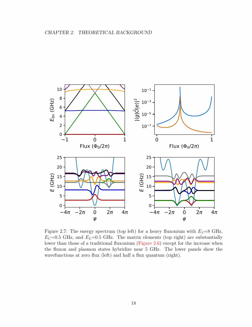
Heavy Fluxonium
The charging energy plays the role of effective mass in the circuit, and by decreasing
EC , we can effectively make the circuit “heavier”, which can be thought of as a lo-
calization of wavefunctions in different cosine potential wells. Traditional fluxonium
circuits use a ratio of EJ/EC between 1 and 5. As EC is further reduced, we enter the
regime of “heavy fluxonium”. The idea of disjoint wavefunctions becomes explorable,
as the effective mass of the qubit is increased and the fluxon states localize in different
potential wells. This has recently been explored [47, 48], and record superconduct-
ing qubit lifetimes exceeding 8 ms have been measured. This can be understood by
looking at the decrease in the phase matrix element between the fluxon states. When
comparing the matrix elements in Figure 2.6 to Figure 2.7, we see that the matrix
element is many orders of magnitude lower at all values of external flux. This opens
up several potential and exciting ideas, chief among them the use of dielectrics neces-
sary for multi-layer qubit fabrication [49, 50]. As the number of qubits continues to
increase, it is certain that multi-layer connectivities will have to be created to avoid
parasitic box modes [51]. Generally the capacitive quality factor of the dielectrics
used for multilayer chips is low enough to substantially impact the T1 of the qubit.
With heavy fluxonium however, we now have a qubit which can be made insensitive
to the quality of the dielectrics used on the chips.
There are several additional considerations that need to be addressed in order for
heavy fluxonium to gain traction as a replacement to the ubiquitous transmon qubit.
Practically speaking, the decrease in EC leads to a frequency crowding between the
levels in different fluxon wells. Fundamentally, this is not an insurmountable problem,
16
CHAPTER 2. THEORETICAL BACKGROUND
but it does require careful parameter choices for EJ , EC , and EL to avoid frequency
collisions between different fluxon and plasmon states. The suppression of the matrix
elements between the fluxon states also makes direct operations between the two
disjoint states challenging, but this can be overcome through the use of multi-tone
Raman transitions [47] or other control schemes for many level systems. The largest
challenge for heavy fluxonium is answering the question “At which flux should the
qubit be operated?”. Traditionally, fluxonium has shown the best T1 and T2 values
when operated at the low frequency flux sweet spot [44, 46, 52]. However, as the qubit
is made heavier, hybridization between the fluxon states at this point is reduced, and
the transition frequency will tend to 0. From eqn. 2.33, we note that coth (~ωq/2kBT )
term will diverge, and the relaxation rate will drastically increase, negating the benefit
of the disjoint wavefunctions. The qubit could be operated at the zero flux point
where the frequency difference is finite, however, here the energy gap between the e−1
and e1 fluxon states closes as the qubit is made heavier, and the gate times become
prohibitively long to prevent leakage from the computational space. All intermediate
flux values are also undesirable as the fluxon transition has a linear flux dispersion
and is sensitive to flux noise through the qubit loop. More theoretical work is needed
to determine if it is possible to find a two node circuit with a set of disjoint and flux
insensitive transitions exists. If these criteria can be simultaneously satisfied, then
we would have a suitable replacement for the transmon.
2.3.5 The 0− π qubit
All the qubits considered so far consist of two nodes, and a single degree of freedom.
The simple structure of these circuits allows for analytic solutions to the spectra and
wavefunctions which is why most of the superconducting qubit work in the last 20
years has focused on two node circuit topologies. However, by increasing number of
17
CHAPTER 2. THEORETICAL BACKGROUND
1 0 1Flux ( 0/2 )
0
2
4
6
8
10
E 0n (
GHz)
0 1Flux ( 0/2 )
10 7
10 5
10 3
10 1
|g|O
|e|2
4 2 0 2 40
5
10
15
20
25
E (G
Hz)
4 2 0 2 40
5
10
15
20
25
E (G
Hz)
Figure 2.7: The energy spectrum (top left) for a heavy fluxonium with EJ=8 GHz,EC=0.5 GHz, and EL=0.5 GHz. The matrix elements (top right) are substantiallylower than those of a traditional fluxonium (Figure 2.6) except for the increase whenthe fluxon and plasmon states hybridize near 5 GHz. The lower panels show thewavefunctions at zero flux (left) and half a flux quantum (right).
18
CHAPTER 2. THEORETICAL BACKGROUND
ECEJ, ECJ EJ, ECJEC
EL
EL41
32
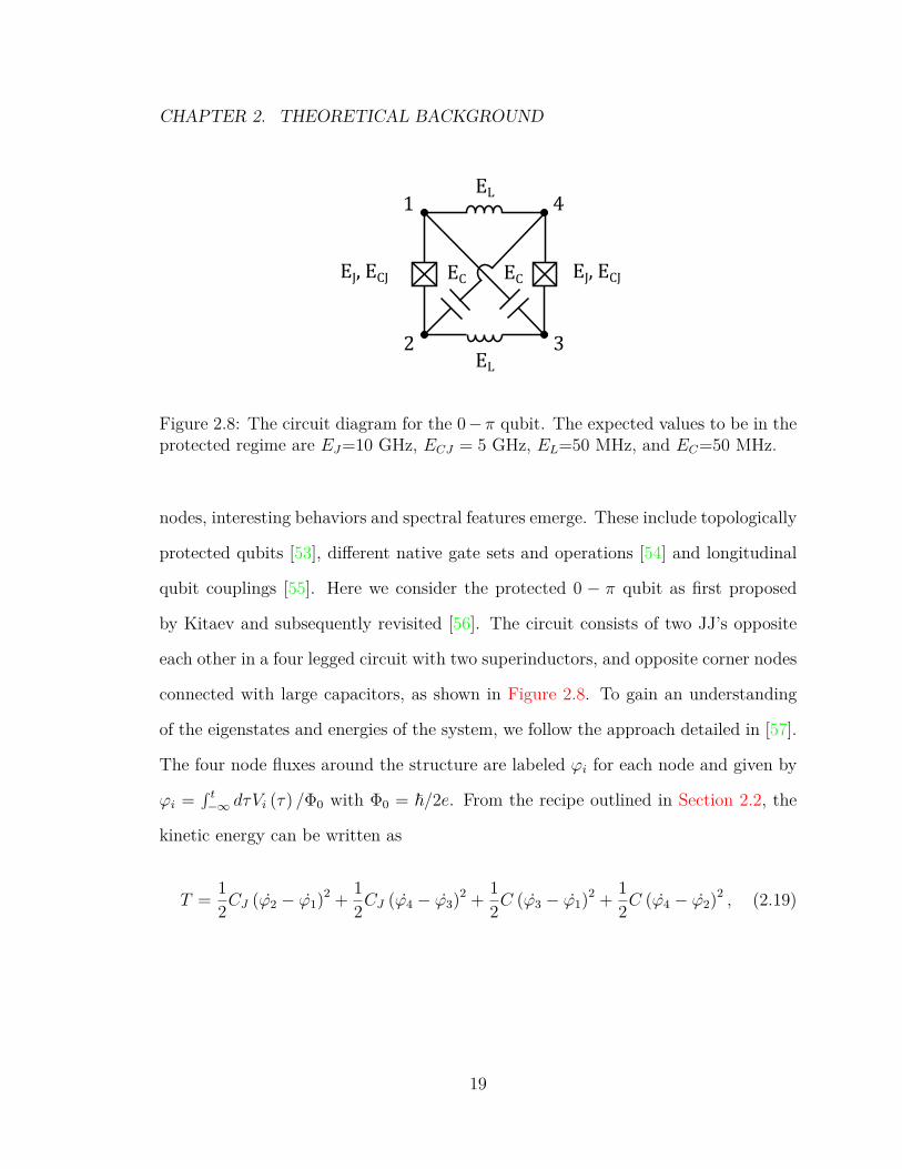
Figure 2.8: The circuit diagram for the 0−π qubit. The expected values to be in theprotected regime are EJ=10 GHz, ECJ = 5 GHz, EL=50 MHz, and EC=50 MHz.
nodes, interesting behaviors and spectral features emerge. These include topologically
protected qubits [53], different native gate sets and operations [54] and longitudinal
qubit couplings [55]. Here we consider the protected 0 − π qubit as first proposed
by Kitaev and subsequently revisited [56]. The circuit consists of two JJ’s opposite
each other in a four legged circuit with two superinductors, and opposite corner nodes
connected with large capacitors, as shown in Figure 2.8. To gain an understanding
of the eigenstates and energies of the system, we follow the approach detailed in [57].
The four node fluxes around the structure are labeled ϕi for each node and given by
ϕi =∫ t−∞ dτVi (τ) /Φ0 with Φ0 = ~/2e. From the recipe outlined in Section 2.2, the
kinetic energy can be written as
T = 12CJ (ϕ2 − ϕ1)2 + 1
2CJ (ϕ4 − ϕ3)2 + 12C (ϕ3 − ϕ1)2 + 1
2C (ϕ4 − ϕ2)2 , (2.19)
19

CHAPTER 2. THEORETICAL BACKGROUND
where CJ is the small JJ capacitance, and C is the capacitance between nodes 1-3
and 2-4. The two superinductors and single JJ’s give the potential terms
U = −EJ cos (ϕ4 − ϕ3 − ϕext/2)− EJ cos (ϕ2 − ϕ1 − ϕext/2)
+ 12EL (ϕ2 − ϕ3)2 + 1
2EL (ϕ4 − ϕ1)2 ,(2.20)
where EJ is the Josephson energy of the single junctions, and EL is the inductive
energy of the superinductors. For notational convenience, we have absorbed the flux
quantum constant into the capacitance and flux variables, C = CΦ20 and ϕext =
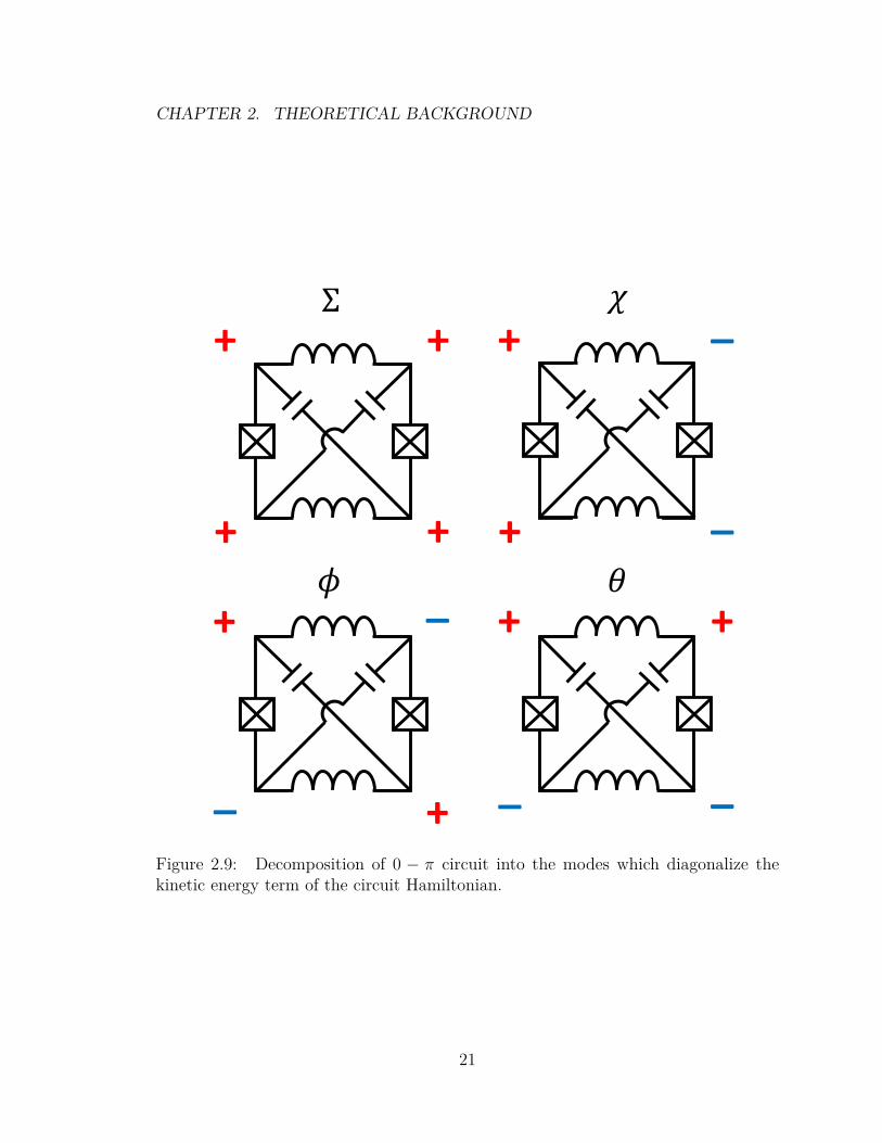
Φext/Φ0. To gain an intuition for the spectra, we can decompose the circuit into
four “modes” of motion, shown in Figure 2.9. By making a change of variables to
diagonalize the kinetic energy term
2φ = (ϕ2 − ϕ3) + (ϕ4 − ϕ1)
2θ = (ϕ2 − ϕ1)− (ϕ4 − ϕ3)
2χ = (ϕ2 − ϕ3)− (ϕ4 − ϕ1)
Σ = ϕ1 + ϕ2 + ϕ3 + ϕ4,
(2.21)
we can rewrite the kinetic and potential energy terms as
T = CJ φ2 + (CJ + C) θ2 + Cχ2, (2.22)
and
U = −2EJ cos θ cos (φ− ϕext/2) + ELφ2 + ELχ
2. (2.23)
By making the variable transformation, we have eliminated one degree of freedom,
the Σ mode, which represents a global shift of the potential at all nodes, leaving us
with the correct, n−1 = 3, degrees of freedom. This choice of variables also highlights
20
CHAPTER 2. THEORETICAL BACKGROUND
+ +
+ +
Σ 𝜒
+ _
+ _
𝜙
+ _
_ +
𝜃+ +
_ _
Figure 2.9: Decomposition of 0 − π circuit into the modes which diagonalize thekinetic energy term of the circuit Hamiltonian.
21

CHAPTER 2. THEORETICAL BACKGROUND
that one of the modes of motion, the χ mode, is decoupled from the small JJ’s, that
is, it’s a purely harmonic variable that oscillates with frequency Ωχ =√
8ELEC/~.
In the absence of disorder, the χ modes will remain uncoupled from the rest of the
spectrum. Experimentally, we expect some degree of disorder from device fabrication
variations; however, as long as the relevant qubit frequencies are kept far from the χ
modes, there is no expected degradation in the lifetime and coherence for the qubit
[58]. The Lagrangian with the remaining two modes of motion for the perfectly
symmetric device is therefore given by
L = CJ ϕ2 + CΣθ
2 + 2EJ cos θ cos (φ− ϕext/2)− ELφ2, (2.24)
where CΣ ≡ (CJ + C). Performing the Legendre transform and canonical quantiza-
tion yields
H = −2EC∂2φ − 2ECΣ∂
2θ − 2EJ cos θ cos (φ− ϕext/2) + ELφ
2 + 2EJ , (2.25)
where the additional factor of 2EJ is included for convenience to have the energy
spectrum always positive. The effective potential of the system is given by V (θ, φ) =
−2EJ cos θ cos (φ− ϕext/2) + ELφ2 + 2EJ and is shown in Figure 2.10. The circuit
receives its name from the two potential wells in the θ direction, with minima at 0 and
π. As originally conceived, the circuit parameters are chosen such that the ground
state and first excited state exist as wavefunctions that are localized in a single θ well
but delocalized over many ϕ wells. As originally conceived the four constraints to be
in the 0− π regime are:
1. ECJ ECΣ
2. EJ ECΣ
22

CHAPTER 2. THEORETICAL BACKGROUND
-4 -2 2 4 0
Figure 2.10: The effective potential, V (θ, φ), for the 0− π qubit at ϕext = 0.
3. EJ EL
4. ECJ EL
Note that EL is the smallest energy scale which must be on the order of 50 MHz or
∼ 3 µH. These constraints, the seemingly contradictory light φ and heavy θ modes
and superinductance values that are in excess of 1 µH, have made the experimental
realization challenging.
Despite the fabrication challenges and complex level structure, the potential in-
crease in T1 and T2 of the 0 − π over existing two node circuits has garnered ex-
perimental interest in recent years. As was recently reported [58], both the T1 and
T2 times are expected to be several orders of magnitude larger than state of the art
transmon values.
To understand the origin of the protection in qubit lifetime and coherence, we con-
sider the ground and first excited state wavefunctions and the 0−π energy spectrum.
As shown in Figure 2.11, the ground and excited states are extremely disjoint, that
is to say, the overlap of the wavefunctions is vanishingly small. This small overlap23

CHAPTER 2. THEORETICAL BACKGROUND
0 /2ext/ 0
0
1
2E
(GHz
)
-4 -2 0 2 40
-4 -2 0 2 40
Figure 2.11: The first few eigenenergies of 0−π plotted as a function of external fluxthrough the qubit loop (top). The |0〉 and |1〉 states are highlighted in gold and greenrespectively. The wavefunctions for the |0〉 (middle) and |1〉 (bottom) states, notethe localization in the 0 and π, θ wells.
24

CHAPTER 2. THEORETICAL BACKGROUND
results in a protection of the excited state lifetime (as is discussed in greater detail in
Section 2.5). The protection in T2 arises from the near degeneracy of the |0〉 and |1〉
states, as the pure dephasing rate between two levels is given by ∂E01/∂λ where E01
is the transition energy between the levels and λ is some external parameter (ie. flux
or charge). This near degeneracy between the states is achieved through constraints
3 and 4.
2.4 Qubit-resonator coupling
To perform state initialization, coherent manipulation, and measurement, we must
couple a probe to our qubits. In traditional cavity QED experiments an atom is
coupled to the field of an single mode in an optical resonator. In the case of circuit
QED, we typically make use of a planar structure, such as a coplanar waveguide
resonator, to capacitively or inductively couple to qubits. Superconducting qubits
can be made in the strong coupling regime, where the coupling strength between
the resonator and the qubit is much greater than either the photon loss rate of the
cavity or the decay rate of the qubit [59, 60]. A qubit coupled to a resonator can be
described by the following Hamiltonian
Htot = Hq +Hr +Hc, (2.26)
where Hq describes the qubit subsystem, Hr the resonator subsystem, and Hc de-
scribes the coupling between the two. We follow the theoretical description of such a
system with a resonator that is capacitively coupled to a superconducting resonator
25

CHAPTER 2. THEORETICAL BACKGROUND
[61] to find
H =∑j
~ωja†jaj +∑l
El|l〉〈l|+∑j
∑l,l′gj;ll′|l〉〈l′|
(aj + a†j
), (2.27)
where ωj is the photon mode frequency, El are the energy levels of the states |l〉 of a
multilevel “qudit” system, and the coupling coefficients, gj;ll′ are given by
gj;ll′ = gj〈l|n|l′〉, (2.28)
where gj = 2eV rmsj Cq/CΣ. In the dispersive regime of cQED [62], the Hamiltonian
can be approximated to second order by
Heff =∑j
~ωja†jaj +∑l
El|l〉〈l|+∑j,l
χj;la†jaj|l〉〈l|+
∑l
κl|l〉〈l|, (2.29)
where the third and fourth terms represent the ac-Stark and Lamb shifts of the qudit
energy levels. We can sum over the partial dispersive shifts χj;ll′ ≡ |gj;ll′ |2/∆j;ll′ ,
where ∆j;ll′ are the resonator mode and qudit energy level detunings, to find the
energy correction in eqn. 2.29,
χj;l =∑l′
(χj;ll′ − χj;l′l) . (2.30)
When the qubit state changes, the change in χj;l will cause the a shift in the microwave
resonator frequency which can be measured through standard microwave transmis-
sion or reflection measurements [63], allowing us to determine the state of the qubit.
Typically, this many level treatment can be simplified for CPB and transmon qubits
where the system can more accurately be approximated with fewer qubit levels, how-
26

CHAPTER 2. THEORETICAL BACKGROUND
I
Y(ω)
Qubit
Figure 2.12: A simplified circuit model for relaxation in the qubit, consisting of acurrent noise source, I (t) and an admittance Y (ω) placed in parallel with the qubit.
ever keeping these corrections is important in understanding highly multilevel systems
such as fluxonium or 0− π.
2.5 Relaxation in qubits
The energy relaxation rate, or T1, is the average rate at which a qubit decays from
its excited state back to the ground state [5]. Understanding relaxation in qubits is
important as it ultimately sets the bound on qubit coherence; T2 = 2T1 in the absence
of dephasing. Relaxation can arise from many different microscopic causes, but can
generally be thought of as coupling between the qubit and a lossy environment, which
will take energy from the qubit. Figure 2.12 shows a simplified general circuit model
for situation, in which the qubit can be placed in parallel to an admittance Y (ω)
consisting of a frequency dependent resistor R, a coupling capacitance CC , and a
fluctuating current, I. This coupling can be expressed in a similar manner as the
resonator coupling in the previous section:
Henv = ΦI = ϕ0ϕI. (2.31)
27
CHAPTER 2. THEORETICAL BACKGROUND
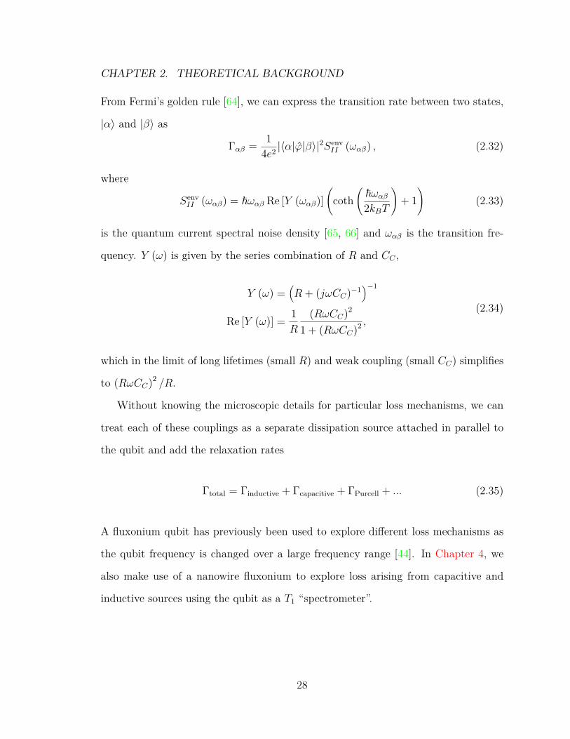
From Fermi’s golden rule [64], we can express the transition rate between two states,
|α〉 and |β〉 as
Γαβ = 14e2 |〈α|ϕ|β〉|
2SenvII (ωαβ) , (2.32)
where
SenvII (ωαβ) = ~ωαβ Re [Y (ωαβ)]
(coth
(~ωαβ2kBT
)+ 1
)(2.33)
is the quantum current spectral noise density [65, 66] and ωαβ is the transition fre-
quency. Y (ω) is given by the series combination of R and CC ,
Y (ω) =(R + (jωCC)−1
)−1
Re [Y (ω)] = 1R
(RωCC)2
1 + (RωCC)2 ,(2.34)
which in the limit of long lifetimes (small R) and weak coupling (small CC) simplifies
to (RωCC)2 /R.
Without knowing the microscopic details for particular loss mechanisms, we can
treat each of these couplings as a separate dissipation source attached in parallel to
the qubit and add the relaxation rates
Γtotal = Γinductive + Γcapacitive + ΓPurcell + ... (2.35)
A fluxonium qubit has previously been used to explore different loss mechanisms as
the qubit frequency is changed over a large frequency range [44]. In Chapter 4, we
also make use of a nanowire fluxonium to explore loss arising from capacitive and
inductive sources using the qubit as a T1 “spectrometer”.
28

CHAPTER 2. THEORETICAL BACKGROUND
2.6 Kinetic Inductance
Inductance has become an increasingly important tool in superconducting circuits,
in particular, the use of superinductors, inductors with Z > RQ, in fluxonium and
0 − π circuits. Previous implementations of superinductors [38] use of arrays of
JJ as the superinductive element. However these carry with them the challenges
of self resonance modes [39], and phase slips across the array junctions limiting T2
[52]. An alternative superinductor construction consists of a high kinetic inductance
nanowire. Kinetic inductance is the inductive like energy that arises from the motion
of charge carriers [23]. All materials have kinetic inductance, however, in practice,
l
d
w
2e
Figure 2.13: In a thin disordered superconducting film, the motion of Cooper pairsgives rise to an increased inductance of the wire. Examples of materials with largeLk include NbN [67], TiN [68], NbTiN [43], and granular Al [69]
for normal metals the mean free path of the electrons makes this contribution an
insignificant fraction compared to the geometric (magnetic) inductance. However,
in disordered superconductors with very low densities of Cooper pairs, this kinetic
inductance contribution can dominate over the geometric inductance of a nanowire
or thin film. The kinetic inductance, Lk, can be expressed as
29

CHAPTER 2. THEORETICAL BACKGROUND
Lk =(
m
2e2ns
)(l
wd
), (2.36)
where ns is the density of Cooper pairs; m is the electron mass; e is the electron
charge; and l, w, d the length, width, and thickness of the wire respectively [67]. Lk
can also be obtained using BCS theory [23] and expressed as
Lk =(l
w
)(Rh
2π2∆
) 1tanh
(∆
2kBT
) . (2.37)
Although equivalent, the BCS expression is more useful in terms of parameters which
are easily to experimentally measure, namely, the sheet resistivity, R, and the su-
perconducting gap, ∆.
30
Chapter 3
Experimental Techniques
Running a cQED experiment requires knowledge and control of systems that range
in length scales from ∼ 100 nm (the nanofabricated JJ’s) to meters (the dilution
refrigerator and room temperature electronics). In this chapter, we provide a descrip-
tion of the fabrication techniques used to fabricate and package qubits, details of the
measurement setup, and a brief overview of the microwave measurement techniques
used to measure devices. We conclude with a characterization of the NbTiN films
used in constructing the nanowire superiductance fluxonium qubit (NSFQ).
3.1 Fabrication
Here we provide an overview of the device fabrication process, for the NSFQ, 0 − π
and the zero ZZ devices, with a more detailed list of cleanroom recipes provided in
Appendix. A. The fabrication processes are nominally identical for the NSFQ and
0 − π compared to the zero ZZ device, with an additional set of steps added for
the patterning of the NbTiN nanowires. Careful cleaning is performed before and
after different fabrication steps to limit the amount of metal and organic residues
on the surface of the device. The main process involves a TAMI (Toluene, Acetone,
Methanol, Isopropanol) clean, sonicating the chips for 2 minutes in each of the in-31
CHAPTER 3. EXPERIMENTAL TECHNIQUES
dividual solvents. For the NSFQ and 0 − π chips, we start with a 500 µm thick
C-plane sapphire with a film of either 10 or 15 nm of NbTiN deposited on the surface
(provided by StarCryo). The chips are covered in UV light sensitive resist (S1811)
and a pattern is directly written on the chip using a Heidelberg DWL-66+ mask
writer in the cleanroom. The exposed resist is removed with a weak base (MF-319)
and the unwanted NbTiN is removed with a fluorine based (SF6:Ar) etch. A sec-
ond photolithography step covers the remaining NbTiN, followed by sputtering an
additional layer of 200 nm thick Nb for the readout resonators, with one additional
photolithography step and fluorine etch to pattern the Nb. Although in principle
the resonators could have been fabricated from the NbTiN, we added the additional
fabrication steps to eliminate any self-Kerr non-linearities from the resonator which
might complicate the device measurements. In future designs, this process could be
modified, and even taken advantage of to make more compact resonators based on
their large kinetic inductance. Once the resonators are patterned and etched, we per-
form e-beam lithography with the Elionix 125 kV e-beam writer, to expose a double
layer of MMA EL13/ PMMA950-A3 e-beam resist with a 40 nm thick Al anti-charge
layer on top of the resist. The MMA has a lower clearing dose than the PMMA and
provides an “undercut” for shadow evaporation of the junctions. Once the e-beam
pattern is written, the anti-charge layer is removed along with the exposed resist,
and the devices are loaded into the Plassys evaporator for evaporation of the JJs.
After evaporation and oxidation of the JJ’s the extraneous Al is removed by soaking
the chips in N-Methyl-2-pyrrolidone for several hours. For fabrication of the zero ZZ
devices, we perform all the steps starting from the deposition of Nb onto a cleaned
sapphire substrate.
32

CHAPTER 3. EXPERIMENTAL TECHNIQUES
3.1.1 Junction types
There are different styles of JJ’s, which we will briefly mention: Dolan bridge junc-
tions [70], cliff junctions [71], and Manhattan junctions [72, 73]. At of the time of this
writing, there is no experimental evidence indicating if any of these junction styles is
superior to the others, although future comprehensive studies might help to elucidate
underlying loss mechanisms present in the design of JJ itself. The choice of junction
is usually based on design considerations, but all three are fabricated on a similar
principle of tilting the sample, evaporating Al, oxidizing the Al, tilting the sample a
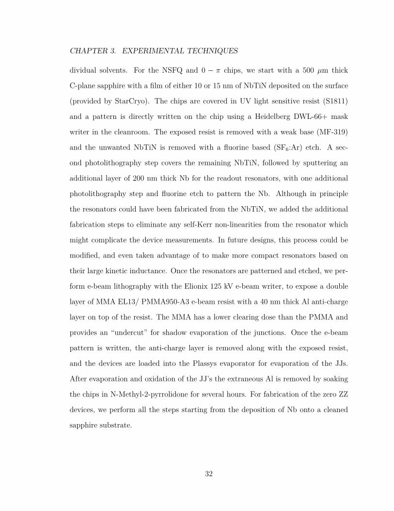
different direction and evaporating a second layer of Al. Figure 3.1 shows the resist
patterns used for the different junction styles. Cliff junctions tend to have a small
amount of extraneous metal and can be made very large (> 0.5 µm2), however the
sensitivity to the undercut and full clear doses make it difficult to fabricate small
junctions with EJ < 8 GHz. Manhattan and Dolan junctions can be reliably fabri-
cated with EJ down to 2 GHz. NSFQ devices 1 and 2 were fabricated with a single
cliff junction each, where as all other 0− π and zero ZZ devices were fabricated with
Manhattan junctions.
3.1.2 Junction resistance
From the Ambegaokar-Baratoff relation [24], we can relate the measured test junction
resistance at room temperature to estimate the EJ of the devices. As the oxide thick-
ness and resistance of the junction depends on the fabrication parameters (oxidation
length, partial pressure of oxygen, quality of Al, etc.), the EJ · Rn constant needs to
be calibrated for each process. Effectively, this is a calibration for variations in ∆
from eqn. 2.4, which would lead to differences from the theoretically predicted 132
kΩ-GHz. Several junctions with different areas are measured to extract an expected
33
CHAPTER 3. EXPERIMENTAL TECHNIQUES
1 μm1
2
1 μm1
2
1 μm
1 2
Manhattan
Cliff
Dolan
Figure 3.1: Several types of JJ’s. The red areas of the schematic are exposed atan e-beam dose high enough to remove both the PMMA and MMA layers of resist(typically ∼ 2000 µC/cm2). Blue areas are exposed at roughly one-fifth the dose,clearing the bottom MMA layer but leaving the top layer intact resulting in a resist“undercut”. The arrows indicate the direction of the evaporation angles, with thesample holder additionally tilted by 40 out of plane for each evaporation. Thescanning electron micrograph (SEM) images have red highlighted segments showingthe JJ area.
34

CHAPTER 3. EXPERIMENTAL TECHNIQUES
Rn per area. Fits of transmon or fluxonium energy spectra are used to verify the
correspondence between EJ and Rn. Table 3.1 has several resistance values for the
witness Manhattan junctions on NSFQ dev 3 chip.
Junction linear dimensions (nm x nm) R (kΩ)100x100 33.6100x100 35.3100x100 35.0125x125 24.2150x150 16.8150x150 16.6150x150 17.5175x175 11.9175x175 11.5175x175 13.1
Table 3.1: Measured test junction resistances at room temperature. From the exper-imentally measured value of EJRn ≈ 120 kΩ-GHz, this range of areas results in EJvalues between 3.5 - 10 GHz.
3.2 Packaging and shielding
Once the sample fabrication is completed, the sample is mounted into a copper disk
(referred to as a “penny”) which has a 7 × 7 mm slot cutout for the chip. Several
of these copper pennies have a ∼ 1 mm deep trench below the sample to reduce
the capacitance between the chip and the sample holder, and to disrupt box modes.
The chip is secured onto the penny with conductive silver paste (Ted Pella 16032)
and mounted with an indium ring pressed onto the printed circuit board. For the
fluxonium and 0 − π samples, a copper wire coil mounted to a spool is screwed
onto the PCB above the surface of the chip, providing external magnetic flux. The
completed sample holder is mounted inside a set of shields consisting of an aluminum
can inside one or two high permeability µ-metal shields. The interior of the aluminum35
CHAPTER 3. EXPERIMENTAL TECHNIQUES
shield is coated with Stycast 2850 (catalyst 23LV) mixed (3:1 by weight) with Silicon
Carbide #16 and #320 grit, to lower the emissivity of the shield interior, reducing
the blackbody radiation emitted from these shields to the sample. The exterior of all
shields is wrapped with aluminized polyethylene terephthalate (trade name of Mylar)
to increase the emissivity of the exterior of the shields. The shields and sample are
attached to the mixing chamber plate of the dilution refrigerator with an OFHC
(oxygen free high conductivity) copper rod. In order to maintain a “light-tight”
shielding enclosure, the measurement wires pass through the shields via several SMA
bulkheads attached to the outer µ-metal can.
3.3 Measurement setup
3.3.1 Dilution Refrigerator
All the measurements presented in this thesis were performed in a BlueFors dilu-
tion refrigerator. The fridge is separated into several temperature stages from room
temperature down to 10 mK. A multi-stage pulse tube cools the first two stages of
the fridge down to ∼50 K and ∼4 K. A mixture of 3He/4He circulates in a separate
closed loop through the still, T = 850 mK, quasi-cold stage, T ∼ 150 mK, and the
mixing chamber, T = 10-20 mK. We make use of the different temperature stages
as thermal anchors for different portions of the measurement setup, including the
filters/attenuators and high electron mobility transistor (HEMT) amplifiers.
3.3.2 Wiring
Keeping qubits isolated from the environment needs careful engineering of the wiring
and microwave setup. The qubits are strongly coupled to microwave cavity resonators
36
CHAPTER 3. EXPERIMENTAL TECHNIQUES
for control and readout which implies that microwave photons in the cavity can have
a significant back-action on the qubits themselves. Thermal photons have been shown
to significantly degrade qubit coherence times as they create Stark shifts in the qubit
energy levels [74, 75]. A lossless transmission line connected from room temperature
down to a device on the mixing chamber sitting at 10 mK would result in a 300 K
noise temperature. To reduce the number of thermal photons, attenuation on the rf
input coaxial cables is configured in such a way as to reduce the effective temperature
of the input line at the resonator, in effect, lowering the temperature of the blackbody
source attached to the resonator. One constraint is the relatively small cooling powers,
∼mW and ∼ µW, at the still and mixing chamber respectively. Additional concerns
have been raised that the center pin of the attenuators is not in thermal equilibrium
with the dilution refrigerator, that dissipating too much power can cause a much
higher effective temperature at the resonator, and that some commercial attenuators
are ineffective at blocking thermal radiation above 20 GHz [76]. Therefore, K&L
12 GHz low pass filters are added to the input/output lines on the mixing chamber
as well as custom Ecosorb absorptive filters. When selecting attenuators, the three
important metrics we consider are total attenuation, final theoretical temperature,
and the power dissipated by the attenuation on the mixing chamber plate. Table 3.2
lists several different possible attenuation setups.
In addition to the cavity input/output lines, the NSFQ and 0 − π devices need
an additional line for biasing the magnetic flux coil. The attenuation setup for the
flux bias line is shown in Figure 3.2. The lines are low pass filtered with Minicircuits
SLP-1.9+ MHz low pass filters. We can calculate the expected magnitude of the
integrated flux noise assuming a Johnson noise source at an some temperature
SV =√
4kBTRδf, (3.1)
37

CHAPTER 3. EXPERIMENTAL TECHNIQUES
Atten. config (dB) PD (µW, 0 dBm input) Tout eff (mK)10, 10, 10, 0, 30 900, 90, 9, 0, 0.99 17.20, 10, 10, 0, 40 0, 900, 90, 0, 9.9 15.50, 0, 20, 20, 20 0, 0, 990, 9.9, 0.099 16.9
Table 3.2: Several fridge attenuator configurations. The sequence of numbers in theattenuator configuration and power dissipation, PD, columns represent the 50 K, 4K, Still, quasi-cold, and mixing chamber stages, assuming temperatures of 50 K, 4 K,850 mK, 150 mK and 15 mK respectively. Note how similar effective temperaturesare achieved, but that for the case of 0, 10, 10, 0, 40 dB the power dissipated at themixing chamber is nearly 10 µW.
where T is the effective temperature of the R = 50 Ω resistor with a system bandwidth
of δf . Assuming a flux loop area of 104 µm2, a noise bandwidth of 2 MHz, a magnet
field constant of 0.1 Gauss/V, and an effective noise temperature of 2 K, we expect a
total integrated flux noise of 5 µΦ0 due to Johnson noise, which is acceptably small.
On the output, we need to keep the cavity isolated as well as collect measurement
photons with as minimal loss as possible before the first amplifier. Based on the Frii’s
equation [77], any loss present between the signal generator, the output port of the
measurement resonator in this case, and the receiver, such as the HEMT amplifier, will
effectively increase the noise temperature of the subsequent amplifier, proportional
to the loss. As an example, 3 dB of loss between the measurement resonator and a
low noise HEMT with a noise temperature of 3 K will effectively increase the noise
temperature of the HEMT to 6 K. It is therefore undesirable to have attenuation on
the output line before the amplifier for thermalization purposes, and we instead use
isolators mounted on the mixing chamber to prevent noise photons from traveling
back to the device. These ferrite based isolators are only frequency matched over a
narrow band, typically 4-8 GHz, and so additional K&L low pass and Ecosorb filters
are added to the lines as well. The coaxial cables from the isolators to the first
HEMT amplifier are constructed with Nb to further reduce the line loss. As long as
38

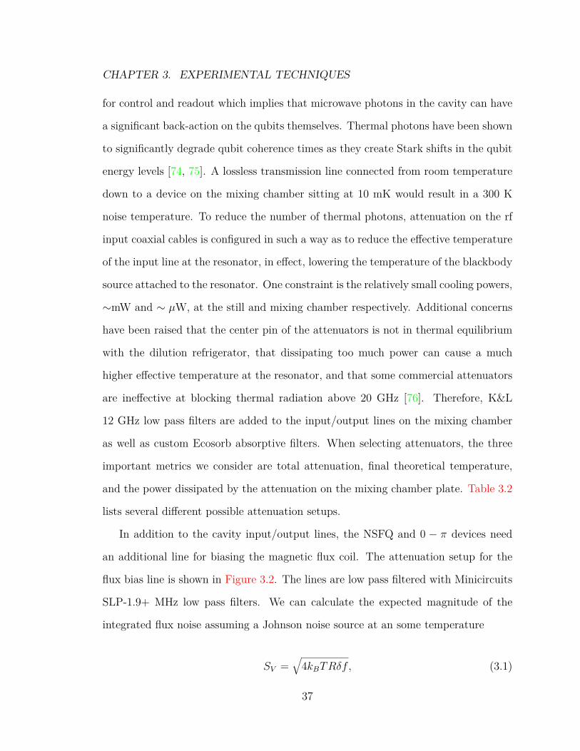
CHAPTER 3. EXPERIMENTAL TECHNIQUES
300 K
50 K
4 K
850 mK
150 mK
15 mK
rf1 dc outputrf2
30 dB
20 dB
10 dB
15 dB
HEMT
Isolator
SS coax
Nb coaxμ-metal (x2), SC shields
K&L LP
Ecosorb
SLP-1.9+
Figure 3.2: A wiring diagram of the fridge used in the experiments. For NSFQ and0− π measurements, attenuation configuration on line “rf1” was used, and “rf2” forthe zero ZZ measurements. All the attenuators are thermalized by fixing them ontoSMA bulkheads screwed into an OFHC copper plate on each stage of the fridge. Forstages without attenuation, thermalization is achieved either through an XMA brand“0 dB” attenuator or by simply mounting to the bulkhead.
the gain of the first amplifier is sufficiently high, its noise contribution will dominate
the output noise of the subsequent readout circuit. Typical measurement powers are
< −100 dBm, therefore several additional Miteq amplifiers (AFS3-00101200-18-10P-
4) are added to get a large enough signal for the fast Analog to Digital Converter
(ADC) or network analyzer.
3.4 Microwave measurement techniques
As discussed in Chapter 2, superconducting qubits are coupled to microwave res-
onators for state preparation, manipulation and readout. Typical resonator frequen-
cies are between 4-10 GHz corresponding to a wavelength of order 10 mm. Here we39
CHAPTER 3. EXPERIMENTAL TECHNIQUES
describe the methods used in understanding simple microwave networks and mea-
surements.
3.4.1 Microwave networks
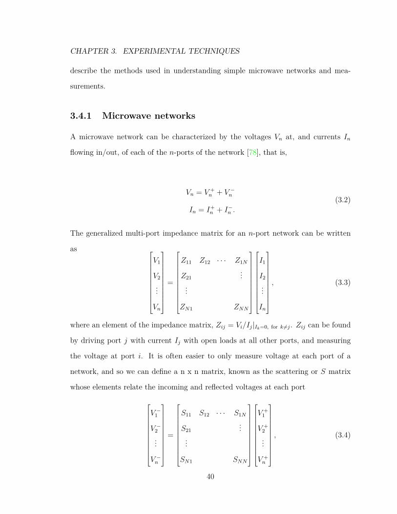
A microwave network can be characterized by the voltages Vn at, and currents In
flowing in/out, of each of the n-ports of the network [78], that is,
Vn = V +n + V −n
In = I+n + I−n .
(3.2)
The generalized multi-port impedance matrix for an n-port network can be written
as
V1
V2
...
Vn
=
Z11 Z12 · · · Z1N
Z21...
...
ZN1 ZNN
I1
I2
...
In
, (3.3)
where an element of the impedance matrix, Zij = Vi/Ij|Ik=0, for k 6=j. Zij can be found
by driving port j with current Ij with open loads at all other ports, and measuring
the voltage at port i. It is often easier to only measure voltage at each port of a
network, and so we can define a n x n matrix, known as the scattering or S matrix
whose elements relate the incoming and reflected voltages at each port
V −1
V −2...
V −n
=
S11 S12 · · · S1N
S21...
...
SN1 SNN
V +1
V +2...
V +n
, (3.4)
40
CHAPTER 3. EXPERIMENTAL TECHNIQUES
where an S-parameter Sij = V −i /V+j |V +
k=0, for k 6=j. One subtle modification to mea-
suring S-parameters is that all unused ports must be terminated with matched loads,
typically Z0 = 50 Ω, in order to enforce V +k = 0. A vector network analyzer is used to
measure the amplitude and phase of the incident and reflected voltages at the differ-
ent ports to measure the S-parameters of a device. A typical microwave setup might
consist of a λ/2 coplanar waveguide resonator with coupling capacitors on the ends
of the resonator. In this situation, the number of ports for each of the elements in the
circuit is two, but having three cascaded elements makes analyzing the circuit with
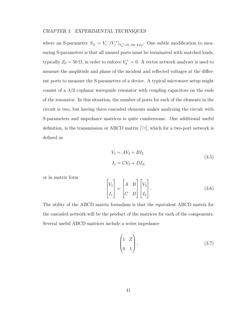
S-parameters and impedance matrices is quite cumbersome. One additional useful
definition, is the transmission or ABCD matrix [78], which for a two-port network is
defined as
V1 = AV2 +BI2
I1 = CV2 +DI2,
(3.5)
or in matrix form V1
I1
=
A B
C D
V2
I2
. (3.6)
The utility of the ABCD matrix formalism is that the equivalent ABCD matrix for
the cascaded network will be the product of the matrices for each of the components.
Several useful ABCD matrices include a series impedance
1 Z
0 1
, (3.7)
41
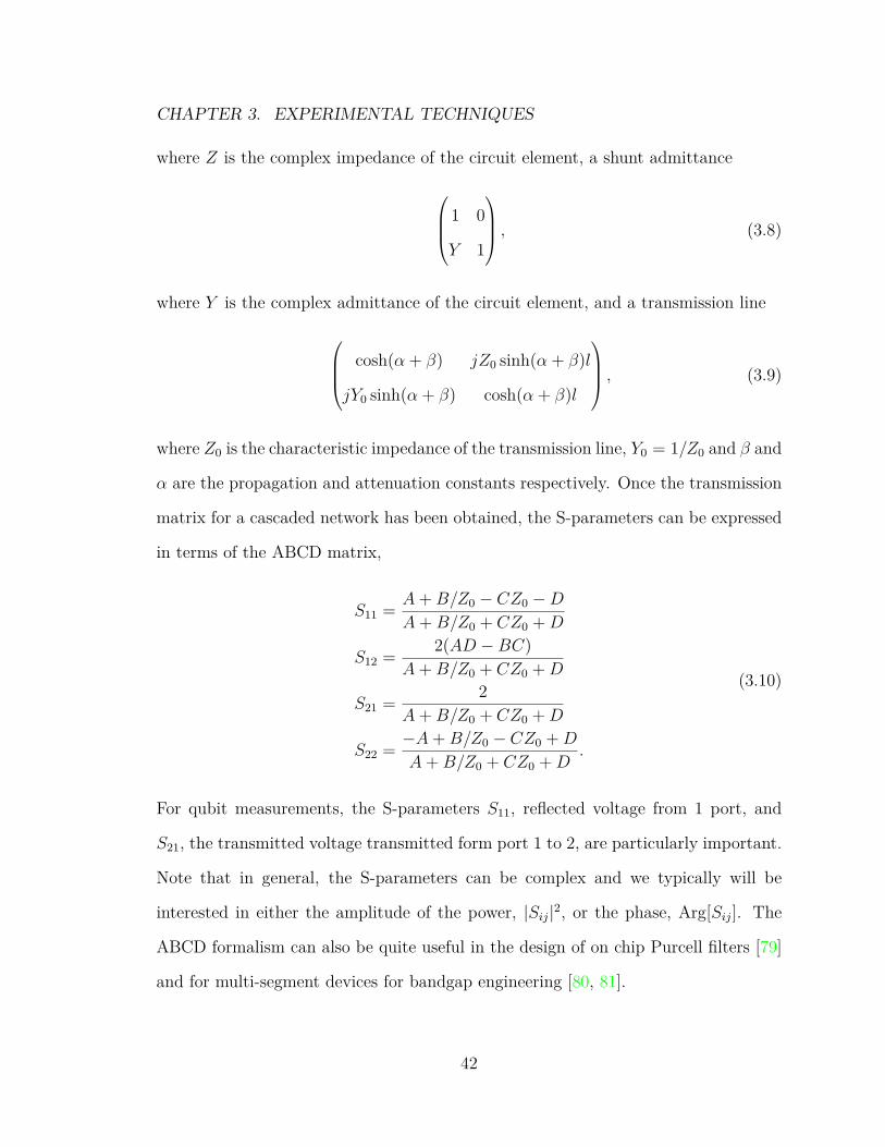
CHAPTER 3. EXPERIMENTAL TECHNIQUES
where Z is the complex impedance of the circuit element, a shunt admittance
1 0
Y 1
, (3.8)
where Y is the complex admittance of the circuit element, and a transmission line
cosh(α + β) jZ0 sinh(α + β)l
jY0 sinh(α + β) cosh(α + β)l
, (3.9)
where Z0 is the characteristic impedance of the transmission line, Y0 = 1/Z0 and β and
α are the propagation and attenuation constants respectively. Once the transmission
matrix for a cascaded network has been obtained, the S-parameters can be expressed
in terms of the ABCD matrix,
S11 = A+B/Z0 − CZ0 −DA+B/Z0 + CZ0 +D
S12 = 2(AD −BC)A+B/Z0 + CZ0 +D
S21 = 2A+B/Z0 + CZ0 +D
S22 = −A+B/Z0 − CZ0 +D
A+B/Z0 + CZ0 +D.
(3.10)
For qubit measurements, the S-parameters S11, reflected voltage from 1 port, and
S21, the transmitted voltage transmitted form port 1 to 2, are particularly important.
Note that in general, the S-parameters can be complex and we typically will be
interested in either the amplitude of the power, |Sij|2, or the phase, Arg[Sij]. The
ABCD formalism can also be quite useful in the design of on chip Purcell filters [79]
and for multi-segment devices for bandgap engineering [80, 81].
42

CHAPTER 3. EXPERIMENTAL TECHNIQUES
3.4.2 CPW resonators
A coplanar waveguide (CPW) consists of a thin superconducting “center pin”, with
width S, placed in a gap with a width W (see Figure 3.3) between two semi-infinite
superconducting ground planes [82]. The system acts as a planar analog to a coaxial
cable, supporting TEM-like propagating modes. The C-plane sapphire substrate has
an anisotropic dielectric constant with εr = 11.5 for fields parallel to the C-axis and
εr = 9.5 for perpendicular fields, and the effective dielectric constant will have an
intermediate value based on the dimensions of the center pin width and gaps which
dictate the electric field distribution in the substrate. The surface above the CPW is
typically vacuum, εr = 1. Through conformal mapping techniques, both εeff and Z0
can be found and are given as
εeff = 1 + εsub − 12
K(k1)K(k′1)
K(k′0)K(k0)
Z0 = 30π√εeff
K(k′0)K(k0) ,
(3.11)
where K(ki) are the complete elliptic integrals of the first kind [82]. The arguments
of the elliptic integrals are given by
k0 = S
S + 2W k′0 =√
1− k20
k1 =sinh
(πS4h
)sinh
(π(S+2W )
4h
) k′1 =√
1− k21
(3.12)
43

CHAPTER 3. EXPERIMENTAL TECHNIQUES
where h is the substrate thickness. From these expressions, we can obtain the char-
acteristic capacitance and inductance per length of the CPW as
L/l = µ0
4K(k′0)K(k0)
C/l = 2ε0 (εsub − 1) K(k1)K(k′1) + 4ε0
K(k0)K(k′0) .
(3.13)
Knowing the characteristic inductance of the CPW will be important in the analysis
of the λ/4 NbTiN resonators to extract the fraction of kinetic inductance arising from
the NbTiN film.
To turn the waveguide into a resonator, the center pin can be either cut in two
locations or cut at one end and terminated via a short to the ground plane on the
other end. These configurations produce standing waves in the center pin with either
a voltage anti-node at each end or a voltage anti-node at one end and a node at the
other end (see Figure 3.3). The gaps on both ends is referred to as a λ/2 resonator
and the single gap with shorted termination is referred to as a λ/4 resonator. The
resonance frequencies are given by
l = λ/2 = ωr = cπ
l√εeff
l = λ/4 = ωr = cπ
2l√εeff. (3.14)
Additional standing wave modes exist at higher frequency harmonics, eg. 3λ/2, 5λ/2,
7λ/2... or 3λ/4, 5λ/4, 7λ/4..., which has important implications for relaxation via
multi-mode Purcell effect [45], and leads to the general rule that the qubit frequencies
should be placed below the fundamental frequency of a multi-mode resonator.
Near resonance, an open circuited λ/2 resonator behaves like a parallel RLC cir-
cuit, with a sharp resonance peak and the λ/4 resonator can be approximated as a
series RLC circuit, near its resonance frequency with an anti-resonance (dip).
44
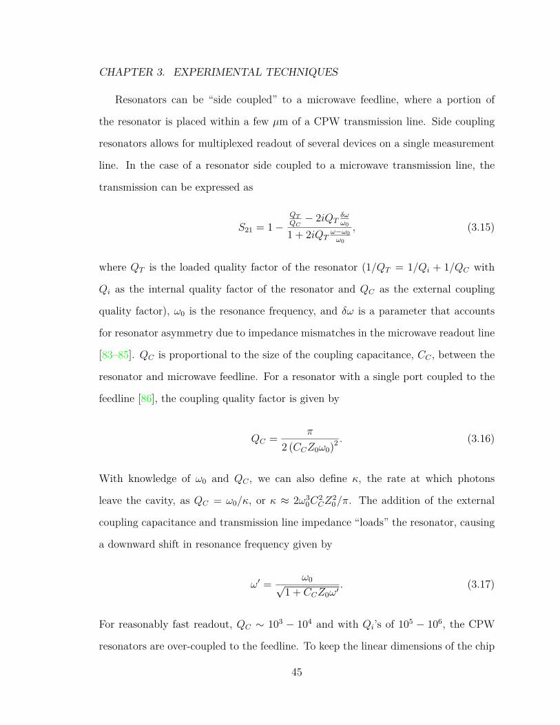
CHAPTER 3. EXPERIMENTAL TECHNIQUES
Resonators can be “side coupled” to a microwave feedline, where a portion of
the resonator is placed within a few µm of a CPW transmission line. Side coupling
resonators allows for multiplexed readout of several devices on a single measurement
line. In the case of a resonator side coupled to a microwave transmission line, the
transmission can be expressed as
S21 = 1−QTQC− 2iQT
δωω0
1 + 2iQTω−ω0ω0
, (3.15)
where QT is the loaded quality factor of the resonator (1/QT = 1/Qi + 1/QC with
Qi as the internal quality factor of the resonator and QC as the external coupling
quality factor), ω0 is the resonance frequency, and δω is a parameter that accounts
for resonator asymmetry due to impedance mismatches in the microwave readout line
[83–85]. QC is proportional to the size of the coupling capacitance, CC , between the
resonator and microwave feedline. For a resonator with a single port coupled to the
feedline [86], the coupling quality factor is given by
QC = π
2 (CCZ0ω0)2 . (3.16)
With knowledge of ω0 and QC , we can also define κ, the rate at which photons
leave the cavity, as QC = ω0/κ, or κ ≈ 2ω30C
2CZ
20/π. The addition of the external
coupling capacitance and transmission line impedance “loads” the resonator, causing
a downward shift in resonance frequency given by
ω′ = ω0√1 + CCZ0ω′
. (3.17)
For reasonably fast readout, QC ∼ 103 − 104 and with Qi’s of 105 − 106, the CPW
resonators are over-coupled to the feedline. To keep the linear dimensions of the chip
45
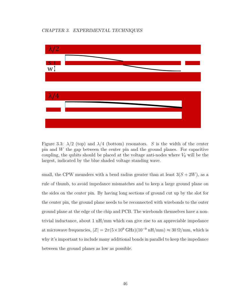
CHAPTER 3. EXPERIMENTAL TECHNIQUES
λ/2
sw
λ/4
Figure 3.3: λ/2 (top) and λ/4 (bottom) resonators. S is the width of the centerpin and W the gap between the center pin and the ground planes. For capacitivecoupling, the qubits should be placed at the voltage anti-nodes where V0 will be thelargest, indicated by the blue shaded voltage standing wave.
small, the CPW meanders with a bend radius greater than at least 3(S + 2W ), as a
rule of thumb, to avoid impedance mismatches and to keep a large ground plane on
the sides on the center pin. By having long sections of ground cut up by the slot for
the center pin, the ground plane needs to be reconnected with wirebonds to the outer
ground plane at the edge of the chip and PCB. The wirebonds themselves have a non-
trivial inductance, about 1 nH/mm which can give rise to an appreciable impedance
at microwave frequencies, |Z| = 2π(5×10⁹ GHz)(10−9 nH/mm) ≈ 30 Ω/mm, which is
why it’s important to include many additional bonds in parallel to keep the impedance
between the ground planes as low as possible.
46

CHAPTER 3. EXPERIMENTAL TECHNIQUES
N5241A- PNAX
Port 1
-20 dB
Port 3 Port 2
ZFRSC-123-S+
To fridge
From fridge
AFS3-00101200-18-10P-4 (x2)
Figure 3.4: The measurement setup for single and two-tone cw spectroscopy mea-surements. Port 3 of the network analyzer can be used for the swept spectroscopytone, while measuring the forward transmission, S21 from the other ports.
3.4.3 Microwave spectroscopy
As discussed in Chapter 2, when a qubit is coupled to a microwave resonator and
changes its state, the dispersive interaction will shift the resonator frequency. If
the resonator is probed at its frequency when the qubit is in the ground state, the
corresponding excited state shift will lead to a change in either the transmitted or
reflected probe tone, resulting in a shift of the amplitude and phase of S21 or S11 [60].
In a typical experiment, the frequency of a single continuous wave (cw) probe tone
is swept to locate the resonator. Once the resonator’s frequency is known, the probe
tone is fixed at this frequency and the frequency of a second spectroscopic, tone is
swept to find the qubit [87]. When the frequency of the spectroscopic tone matches
the qubit frequency, the steady-state population of the qubit changes from its ground
state to some fraction in the excited state resulting in a change in the measured S-
parameter. This “two-tone” qubit spectroscopy can be repeated for different values
of some control parameter, such as ng or Φext for voltage or flux tunable qubits,
respectively. Once the qubit and cavity frequencies are known, the system can be
setup for pulsed measurements.
47

CHAPTER 3. EXPERIMENTAL TECHNIQUES
Miteq amp
AWG
Mixer
vector source
Yokogowa GS200
LO
Digitizer
FS 725
analog source
33250 Rb clock
M9018A
HS9004A
E8267D
rf
dc voltage
trigger
33250 10 MHz clock
fridge
U1082A
I Q
Figure 3.5: A block diagram for pulsed measurements. For NSFQ and 0−π samples,the M9018A AWG was replaced with a Tektronix 5014C. The additional 33250 10MHz clock is needed to provide a 3 Vpp 10 MHz reference for the U1082A fast ADC.For the zero ZZ experiments, the LO phase is adjusted to put all the signal in onequadrature (for homodyne) so that both qubits can be simultaneously measured withthe single ADC card.
3.4.4 Pulsed measurements
Pulsed measurements consist of separating the qubit excitation pulse and the read-
out pulse in time. This allows us to measure dynamical properties, such as qubit
relaxation T1 and dephasing T2. A typical measurement cycle consists of a pulse
sequence, eg. a π rotation around the x-axis of the Bloch sphere (Xπ), followed
by a short (< 10 µs) measurement pulse at the resonator frequency. This cycle is
typically repeated on the order of 104 times, and the results are then averaged to
achieve an acceptable SNR [88]. In a pulsed measurement, the readout signal from
the fridge is amplified at room temperature and combined with a local oscillator (LO)
signal and mixed down for homodyne (LO=rf) or heterodyne (LO=rf+Intermediate
48

CHAPTER 3. EXPERIMENTAL TECHNIQUES
Frequency) measurements. After the frequency down conversion, the demodulated
signal is further amplified to get an appropriately sized signal and digitized by a fast
ADC. It’s important to consider the ADC full scale and bit resolution to avoid clip-
ping, when the signal exceeds the full scale range of the ADC, and digitization noise,
when the signal is comparable to the voltage bin size. In homodyne measurements, a
few µs of data are averaged together to obtain a single amplitude (or phase), and for
heterodyne, the measurement data is digitized and “digitally” down converted [89].
3.5 Characterization of NbTiN films
3.5.1 Sheet resistance and Tc
The NbTiN films are deposited on a 500 µm thick C-plane sapphire substrate from
StarCryo, who provide an estimate of the film’s sheet resistance. In order to verify this
measurement and determine how the resistance changes after processing the NbTiN
films, we incorporate a set of test structures on the side of each chip, which consists
of a set of wires with fixed length and varying width. The measured resistances are
fit to the form
R = Rl
w + ∆w, (3.18)
where l is the length of wire, R is the wire sheet resistance, w the width, and ∆w a
parameter that reflects the difference in the designed width compared to the actual
width. ∆w arises from the over/under exposure and developing of the e-beam resist
and the run to run differences in the fluorine etch. For w ∆w, this correction is
small, however for wires less than ∼100 nm in width, this correction is necessary to
accurately estimate the kinetic inductance. Independent SEM images of the wires
confirm that the typical ∆w is around 30 nm. These structures are valuable for rapid
49

CHAPTER 3. EXPERIMENTAL TECHNIQUES
200 400 600 800Wire Width (nm)
0
50
100
150
200R
(k)
Rsq = 94w = 42 nm
80 100 120 140Wire Width (nm)
200
250
300
350
400
450
R (k
)
Rsq = 223w = 30 nm
Figure 3.6: The room temperature resistances for the 15 (left) and 10 (right) nmthick NbTiN films. All the test wires have l = 100 µm. The difference in ∆w is dueto cleanroom process drifts in the ∼6 months between the two fabrication runs.
feedback of fabrication variations and as a rough film characterization for development
of different materials for high Lk applications.
Figure 3.6 shows the characterization on two sets of NbTiN films with different
thickness. To find the critical temperature, TC , of the 15 nm thick film, one of the
test structures was bonded into a PCB and cooled off in a helium flow cryostat and
measured to find TC = 9.5 K.
3.5.2 Resonators
In order to characterize the microwave properties of the 15 nm thick NbTiN film, we
fabricated a set of side-coupled λ/4 CPW resonators. Transmission measurements
at T =15 mK give an LK of 14 pH/. Based on the other material parameters,
the extracted London penetration depth [23] is λ = 440 nm. This is within 7 %
and 2% of the values extracted from the spectra of NSFQ 1 and 2 respectively. The
numbers listed in Table 3.3 are taken at low power where the self-Kerr contribution
50
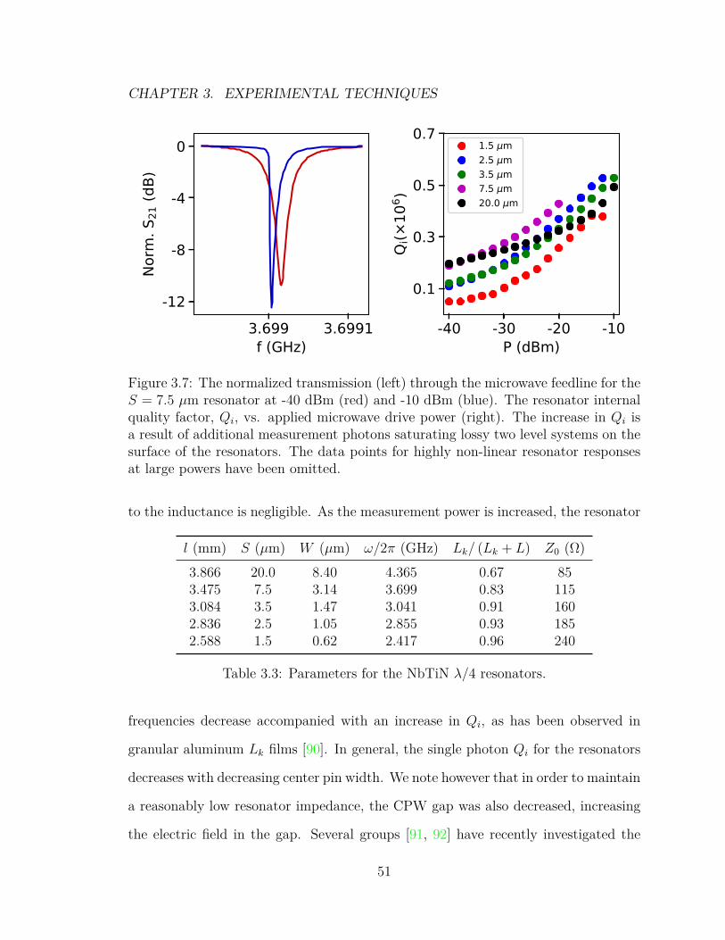
CHAPTER 3. EXPERIMENTAL TECHNIQUES
3.699 3.6991f (GHz)
0
-4
-8
-12
Norm
. S21
(dB)
-40 -30 -20 -10P (dBm)
0.1
0.3
0.5
0.7
Q i(×
106 )
1.5 m2.5 m3.5 m7.5 m20.0 m
Figure 3.7: The normalized transmission (left) through the microwave feedline for theS = 7.5 µm resonator at -40 dBm (red) and -10 dBm (blue). The resonator internalquality factor, Qi, vs. applied microwave drive power (right). The increase in Qi isa result of additional measurement photons saturating lossy two level systems on thesurface of the resonators. The data points for highly non-linear resonator responsesat large powers have been omitted.
to the inductance is negligible. As the measurement power is increased, the resonator
l (mm) S (µm) W (µm) ω/2π (GHz) Lk/ (Lk + L) Z0 (Ω)3.866 20.0 8.40 4.365 0.67 853.475 7.5 3.14 3.699 0.83 1153.084 3.5 1.47 3.041 0.91 1602.836 2.5 1.05 2.855 0.93 1852.588 1.5 0.62 2.417 0.96 240
Table 3.3: Parameters for the NbTiN λ/4 resonators.
frequencies decrease accompanied with an increase in Qi, as has been observed in
granular aluminum Lk films [90]. In general, the single photon Qi for the resonators
decreases with decreasing center pin width. We note however that in order to maintain
a reasonably low resonator impedance, the CPW gap was also decreased, increasing
the electric field in the gap. Several groups [91, 92] have recently investigated the
51

CHAPTER 3. EXPERIMENTAL TECHNIQUES
contribution of loss mechanisms from different interfaces in these structures which
could prove useful for determining the contribution of internal loss from the NbTiN.
52

Chapter 4
Nanowire Superinductance Fluxo-
nium Qubit
The development of superinductors [38, 93] has received significant interest due to
their potential to provide noise protection in superconducting qubits [53, 56, 94].
Moreover, inductively shunted Josephson junction based superconducting circuits are
known to be immune to charge noise [38], and to flux noise in the limit of large
inductances [47, 48, 57, 58]. Despite remarkable progress, the superinductances that
have been so far reported in the literature are still small compared to those needed
for qubit protection. Additionally, Josephson junction array based superinductors are
susceptible to phase slips [52] and junction array modes [39] which complicate the level
structure and potentially lead to additional sources of decoherence and relaxation.
A thin-film nanowire built from a disordered superconductor constitutes an alter-
native approach to reach the required superinductance regime. We demonstrate a
fluxonium circuit integrating a NbTiN nanowire superinductance, and we character-
ize the effect of the nanowire modes on the qubit spectrum with a multimode circuit
theory accounting for the distributed nature of the superinductance.
53

CHAPTER 4. NANOWIRE SUPERINDUCTANCE FLUXONIUM QUBIT
4.1 Device design
A simplified circuit schematic of the nanowire superinductance fluxonium is shown in
Figure 4.1 (a). A small patch of NbTiN, where the nanowire will be fabricated later
in the process, is protected with MicropositTM S1811 photoresist and the remaining
NbTiN is removed with an SF6:Ar dry etch. For the lumped element readout resonator
and transmission line, 200 nm of Nb is sputtered over the areas of the chip which had
no NbTiN and subsequently patterned and etched with another SF6:Ar step. Next,
a layer of ZEP520A (1:1 dilution in anisole) e-beam resist is spun on the chip and
the nanowire pattern is exposed and developed with standard e-beam lithography
techniques. Finally, an MMA/PMMA bilayer e-beam resist is placed on the chip
and the Josephson junction layer is patterned with e-beam lithography. To ensure
metallic contact between the junction and the NbTiN nanowire, a 400 V Ar ion beam
milling process is applied for 45 seconds to remove the native oxide layer formed on
the surface of the NbTiN film. The JJ layer is then immediately fabricated with a
double angle evaporation of 30 nm and 60 nm of Al, with a 15 minute oxidation step
in between the first and second evaporation angles to form the oxide layer of the
junction.
We present data from measurements of three devices fabricated on two different
films. The nanowires in devices 1 and 2 have widths of 110 and 40 nm, respectively,
equal lengths of 730µm and a film thickness of 15 nm. The nanowire in device 3 is
fabricated on a 10 nm thick film, has a width of 100 nm and length of 630µm. The
qubit on devices 1 and 2 is capacitively coupled to a lumped element Nb resonator,
with resonance frequency ωr/2π = 6.08 GHz and a loaded quality factor of QT =
8, 400. The qubit on device 3 is coupled to a half-wavelength coplanar waveguide
54
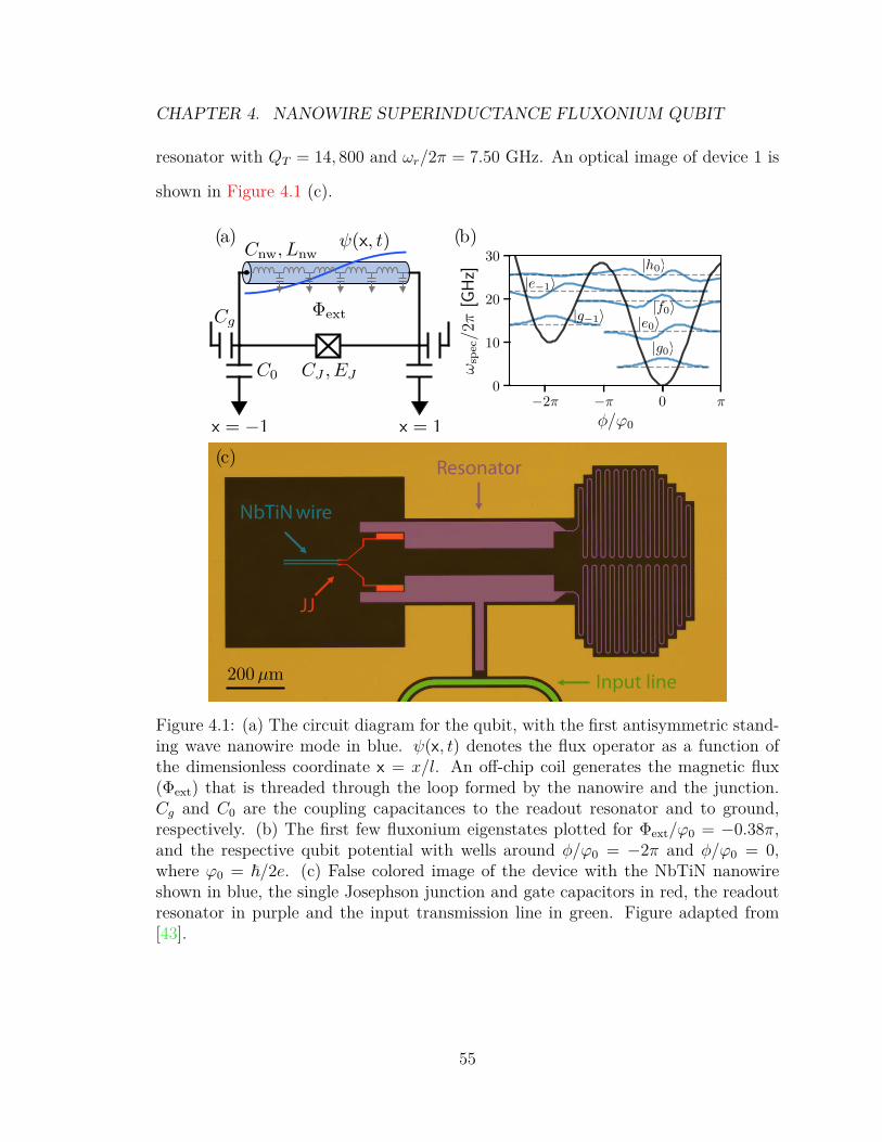
CHAPTER 4. NANOWIRE SUPERINDUCTANCE FLUXONIUM QUBIT
resonator with QT = 14, 800 and ωr/2π = 7.50 GHz. An optical image of device 1 is
shown in Figure 4.1 (c).
−2π −π 0 π
φ/ϕ0
0
10
20
30
ωsp
ec/2π[GHz]
Resonator
NbTiN wire
JJ
Input line
(a) (b)
(c)
Figure 4.1: (a) The circuit diagram for the qubit, with the first antisymmetric stand-ing wave nanowire mode in blue. ψ(x, t) denotes the flux operator as a function ofthe dimensionless coordinate x = x/l. An off-chip coil generates the magnetic flux(Φext) that is threaded through the loop formed by the nanowire and the junction.Cg and C0 are the coupling capacitances to the readout resonator and to ground,respectively. (b) The first few fluxonium eigenstates plotted for Φext/ϕ0 = −0.38π,and the respective qubit potential with wells around φ/ϕ0 = −2π and φ/ϕ0 = 0,where ϕ0 = ~/2e. (c) False colored image of the device with the NbTiN nanowireshown in blue, the single Josephson junction and gate capacitors in red, the readoutresonator in purple and the input transmission line in green. Figure adapted from[43].
55

CHAPTER 4. NANOWIRE SUPERINDUCTANCE FLUXONIUM QUBIT
4.2 Spectrum measurement
The fluxonium energy spectrum is obtained by performing two-tone spectroscopy
measurements as a function of the external magnetic flux, Φext. The amplitude of
the transmitted power is monitored at the dressed cavity frequency while sweeping
a second spectroscopic tone of frequency ωspec/2π. The measurement results are
shown in Figure 4.2. Labeling the energy eigenstates within a single potential well as
|gi〉 , |ei〉 , |fi〉 , ..., where the index i indicates the potential well to which these belong
[see Figure 4.1 (b)], the fluxonium transitions are classified in two types: intra-well
plasmons, such as |g0〉 → |e0〉 , and inter-well fluxons, such as |g0〉 → |g−1〉. Parity
selection rules of the fluxonium circuit allow for transitions between adjacent plasmon
states by absorption of a single photon. However, the direct transition |g0〉 → |f0〉 can
only be completed via a two-photon process in which |e0〉 serves as an intermediate
virtual state. We note that devices 1 and 2 operate in a similar parameter regime to
“heavy fluxonium” [47, 48], where the ratio between the Josephson (EJ) and charging
(EC) energies is large. As a consequence, transitions between the fluxonium potential
wells are exponentially attenuated. Therefore, such excitations are most clearly visible
in the regions where they hybridize with the plasmon energy levels.
Figure 4.2 (a) shows the presence of a second fluxonium mode for device 1 at 16.3
GHz. While similar characteristics have been observed in previous fluxonium devices,
high-frequency modes have been so far phenomenologically modeled as harmonic os-
cillators linearly coupled to the qubit degree of freedom [38]. Here we go beyond such
an approximation and derive a multimode Hamiltonian considering the complete de-
vice Lagrangian, which accounts for the distributed nature of the superinductance.
Importantly, we find that the qubit spectrum is determined by the nonlinear inter-
action of the circuit modes which are antisymmetric at the Josephson junction ports
56

CHAPTER 4. NANOWIRE SUPERINDUCTANCE FLUXONIUM QUBIT
[see Figure 4.1 (a)]. The agreement with the measured data is excellent over a very
large frequency range.
(a) (b)
Figure 4.2: Two-tone spectroscopy of device 1 (a) and device 2 (b) as a functionof Φext. The experimentally measured transition frequencies are indicated with bluemarkers. The result of a fit to the two-mode Hamiltonian in eqn. 4.4, is shown with reddashed lines corresponding to the fluxonium spectrum and with purple dashed linesindicating sideband transitions [95]. In (a), the inscription “JJ mode” (Josephsonjunction mode) identifies the second antisymmetric nanowire mode. Figure adaptedfrom [43].
In contrast to standard fluxonium devices, where a lumped element inductor
shunts the Josephson junction, our circuit model takes into account the fact that the
nanowire superinductor is a high-impedance transmission line. The nanowire is de-
scribed as a homogeneous transmission line with distributed capacitance c = Cnw/2l
and inductance l = Lnw/2l, where Cnw, Lnw and 2l are, respectively, the total ground57

CHAPTER 4. NANOWIRE SUPERINDUCTANCE FLUXONIUM QUBIT
capacitance, inductance and length of the nanowire. Defining the flux operator ψ(x, t)
in terms of the dimensionless coordinate x = x/l, the nanowire Lagrangian can be
written as
Lnw =∫ 1
−1dx (Cnw/2)
2 ψ(x, t)2 − 12(Lnw/2)ψ(x, t)2. (4.1)
Additionally, we consider gate capacitances (Cg) placed at the two ports of the device
(xp = ±1) with respective driving voltages Vxp, as well as ground capacitances (C0).
The Lagrangian of the inductively shunted Josephson junction then reads
L =∑xp
Cg2(ψ(xp, t)− Vxp
)2+ C0
2 ψ(xp, t)2
+ Lnw + CJ2 δψ(t)2 + EJ cos(δψ(t)/ϕ0),
(4.2)
where
δψ(t)/ϕ0 = (∆ψ(t) + Φext)/ϕ0, (4.3)
is the gauge-invariant superconducting phase difference across the junction, ∆ψ(t) =
ψ(1, t)−ψ(−1, t) is the flux operator difference at the boundaries of the superinductor,
and EJ is the Josephson energy [96, 97].
To obtain a tractable theoretical description of our device, we map eqn. 4.2 into
the Lagrangian of an infinite number of nonlinearly interacting normal modes. We
observe that modes which are symmetric at the junction ports are not coupled to
the Josephson nonlinearity, and thus do not contribute to the qubit Hamiltonian.
We therefore derive a multimode Hamiltonian for the antisymmetric normal modes,
which is later truncated to a finite number of modes. The truncation is possible due
to the fact that only few antisymmetric modes lie in the frequency range of interest.
Furthermore, the effective normal mode impedance decreases quickly with the mode
number such that high-frequency modes are only weakly anharmonic.
58
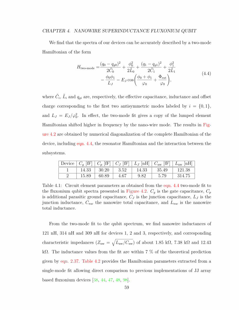
CHAPTER 4. NANOWIRE SUPERINDUCTANCE FLUXONIUM QUBIT
We find that the spectra of our devices can be accurately described by a two-mode
Hamiltonian of the form
Htwo-mode =(q0 − qg0)2
2C0+ φ2
0
2L0+ (q1 − qg1)2
2C1+ φ2
1
2L1
− φ0φ1
LJ− EJ cos
(φ0 + φ1
ϕ0+ Φext
ϕ0
),
(4.4)
where Ci, Li and qgi are, respectively, the effective capacitance, inductance and offset
charge corresponding to the first two antisymmetric modes labeled by i = 0, 1,
and LJ = EJ/ϕ20. In effect, the two-mode fit gives a copy of the lumped element
Hamiltonian shifted higher in frequency by the nano-wire mode. The results in Fig-
ure 4.2 are obtained by numerical diagonalization of the complete Hamiltonian of the
device, including eqn. 4.4, the resonator Hamiltonian and the interaction between the
subsystems.
Device Cg [fF] Cp [fF] CJ [fF] LJ [nH] Cnw [fF] Lnw [nH]1 14.33 30.20 3.52 14.33 35.49 121.382 15.89 60.89 4.67 9.82 5.79 314.75
Table 4.1: Circuit element parameters as obtained from the eqn. 4.4 two-mode fit tothe fluxonium qubit spectra presented in Figure 4.2. Cg is the gate capacitance, Cpis additional parasitic ground capacitance, CJ is the junction capacitance, LJ is thejunction inductance, Cnw the nanowire total capacitance, and Lnw is the nanowiretotal inductance.
From the two-mode fit to the qubit spectrum, we find nanowire inductances of
121 nH, 314 nH and 309 nH for devices 1, 2 and 3, respectively, and corresponding
characteristic impedances (Znw =√Lnw/Cnw) of about 1.85 kΩ, 7.38 kΩ and 12.43
kΩ. The inductance values from the fit are within 7 % of the theoretical prediction
given by eqn. 2.37. Table 4.2 provides the Hamiltonian parameters extracted from a
single-mode fit allowing direct comparison to previous implementations of JJ array
based fluxonium devices [38, 44, 47, 48, 98].59

CHAPTER 4. NANOWIRE SUPERINDUCTANCE FLUXONIUM QUBIT
Device EC [GHz] EL [GHz] EJ [GHz]1 0.89 1.37 10.952 0.56 0.52 16.163 1.90 0.53 5.90
Table 4.2: Device parameter table obtained a single-mode approximate fit to thefluxonium qubit spectrum, for devices 1, 2, and 3.
4.3 Multilevel spectroscopy
In devices 1 and 2, the small dipole element between the fluxon states makes it
experimentally challenging to directly drive the |g−1〉 → |g0〉 transition. By using
multiple drives, we are able to transfer the ground state population between the
neighboring wells using the intermediate |h0〉 state, which is located close to the top
of the barrier and has spectral weight in both wells. We apply three coherent and
simultaneous drives of frequencies ωα/2π, ωβ/2π and ωγ/2π, respectively, targeting
the |g0〉 → |f0〉 (two-photon), the |f0〉 → |h0〉 (one-photon) and the |h0〉 → |e−1〉
(one-photon) transitions [see Figure 4.3(a)].
At Φext/ϕ0 = −0.46π, we set Ωγ = 0 and simultaneously vary ωα/2π and ωβ/2π
around the |g0〉 → |f0〉 and |f0〉 → |h0〉 transitions. We observe a vertical band
corresponding to the |g0〉 → |f0〉 transition at 7.8 GHz, and a diagonal band with a
slope of ωα/ωβ = −1/2, corresponding to the Raman transition between the |g0〉 and
|h0〉 states [Figure 4.3 (a)]. Around the resonance condition (2~ωα ≈ Ef0 − Eg0 and
~ωβ ≈ Eh0 − Ef0), the two bands exhibit an avoided crossing, which is the hallmark
of the Autler-Townes doublet previously observed in other superconducting qubits
[99–102]. Next, we fix the frequency of the α tone at ∆α/2π = 20 MHz, turn on the
γ drive and simultaneously scan the frequencies ωβ/2π and ωγ/2π. Figure 4.3 (b)
displays the resulting Autler-Townes splitting, where the Raman transition manifests
itself here with a slope of ωγ/ωβ = +1, corresponding to the three-drive Raman
60

CHAPTER 4. NANOWIRE SUPERINDUCTANCE FLUXONIUM QUBIT
condition. This method allows us to experimentally determine the energy levels of
the fluxonium qubit using population transfer.
The system can be modeled with a four-level Hamiltonian which, in the
(|g0〉 , |f0〉 , |h0〉 , |e−1〉) energy eigenbasis and in the absence of external drives,
reads
H0 =Eg0 |g0〉 〈g0|+ Ef0 |f0〉 〈f0|+
Eh0 |h0〉 〈h0|+ Ee−1 |e−1〉 〈e−1| , (4.5)
where the groundstate energy is chosen to be Eg0 = 0, and the energies of excited
levels satisfy the relations Eg0 < Ef0 , Ee−1 < Eh0 [see Figure 4.3 (c)]. We work in
a semiclassical picture where the external drives ωα/2π, ωβ/2π, ωγ/2π with respec-
tive Rabi frequencies Ωα, Ωβ, Ωγ introduce coupling exclusively between neighboring
energy levels. In the rotating-wave approximation, this situation is described by the
interaction Hamiltonian
Hint =12~Ωα
(|f0〉 〈g0| e−i2ωαt + |g0〉 〈f0| ei2ωαt
)+
12~Ωβ
(|h0〉 〈f0| e−iωβt + |f0〉 〈h0| eiωβt
)+
12~Ωγ
(|e−1〉 〈h0| eiωγt + |h0〉 〈e−1| e−iωγt
). (4.6)
Since Eh0 > Ee−1 , the time-dependent phase corresponding to the third term in
eqn. 4.6 has the opposite sign. Combining the above expressions, the total Hamilto-
nian of the system is defined as H = H0 +Hint
61

CHAPTER 4. NANOWIRE SUPERINDUCTANCE FLUXONIUM QUBIT
0 60 120 180
twait[µs]
0.001
0.028
Hom
odyn
evo
lt.[arb.]
T1g−1 = 20µs
7.76 7.84ωα/2π [GHz]
4.71
4.89
ωβ/2
π[GHz]
−2 0 2 4 6
S21 [dB]
4.75 4.95ωβ/2π [GHz]
6.82
6.94
ωγ/2
π[GHz]
−2 −1 0 1 2
S21 [dB]
(a) (b)
(c) (d)
Figure 4.3: The multitone spectroscopy data, taken at Φext/ϕ0 = −0.46π, demon-strating population transfer between |g0〉 and |h0〉 (a) with Ωγ = 0, and |h0〉 to |e−1〉(b) with fixed ωα/2π = 7.78 GHz. The white dashed lines indicate the maximumpopulation from a multi-level master equation simulation eqn. 4.9. (c) A schematicdiagram of the device 2 level structure in the presence of coherent external drives.The drives, with frequencies ωi/2π and amplitudes Ωi are detuned from the levels by∆i/2π. (d) Three sequential π pulses (σ = 15 ns) are applied at the transition fre-quencies to perform T1 measurements of the |g−1〉 state. The demodulated homodynevoltage from the readout resonator is measured as a function of twait. Figure adaptedfrom [43].
62
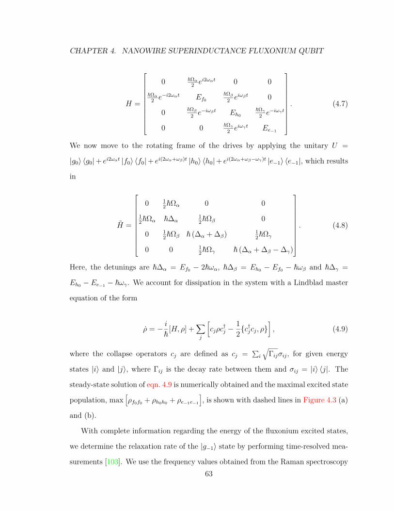
CHAPTER 4. NANOWIRE SUPERINDUCTANCE FLUXONIUM QUBIT
H =
0 ~Ωα2 ei2ωαt 0 0
~Ωα2 e−i2ωαt Ef0
~Ωβ2 eiωβt 0
0 ~Ωβ2 e−iωβt Eh0
~Ωγ2 e−iωγt
0 0 ~Ωγ2 eiωγt Ee−1
. (4.7)
We now move to the rotating frame of the drives by applying the unitary U =
|g0〉 〈g0|+ ei2ωαt |f0〉 〈f0|+ ei(2ωα+ωβ)t |h0〉 〈h0|+ ei(2ωα+ωβ−ωγ)t |e−1〉 〈e−1|, which results
in
H =
0 12~Ωα 0 0
12~Ωα ~∆α
12~Ωβ 0
0 12~Ωβ ~ (∆α + ∆β) 1
2~Ωγ
0 0 12~Ωγ ~ (∆α + ∆β −∆γ)
. (4.8)
Here, the detunings are ~∆α = Ef0 − 2~ωα, ~∆β = Eh0 − Ef0 − ~ωβ and ~∆γ =
Eh0 − Ee−1 − ~ωγ. We account for dissipation in the system with a Lindblad master
equation of the form
ρ = − i~
[H, ρ] +∑j
[cjρc
†j −
12c
†jcj, ρ
], (4.9)
where the collapse operators cj are defined as cj = ∑i
√Γijσij, for given energy
states |i〉 and |j〉, where Γij is the decay rate between them and σij = |i〉 〈j|. The
steady-state solution of eqn. 4.9 is numerically obtained and the maximal excited state
population, max[ρf0f0 + ρh0h0 + ρe−1e−1
], is shown with dashed lines in Figure 4.3 (a)
and (b).
With complete information regarding the energy of the fluxonium excited states,
we determine the relaxation rate of the |g−1〉 state by performing time-resolved mea-
surements [103]. We use the frequency values obtained from the Raman spectroscopy63
CHAPTER 4. NANOWIRE SUPERINDUCTANCE FLUXONIUM QUBIT
and perform a pulse sequence which consists of three sequential π-pulses at the tran-
sition frequencies (Ef0 − Eg0) /h, (Eh0 − Ef0) /h and(Eh0 − Ee−1
)/h to prepare the
system in the |e−1〉 state. At the end of this procedure, the system relaxes into the
|g−1〉 state, on the time scale of the plasmon T1 (∼ 600 ns). On a longer timescale,
the system relaxes back to |g0〉. For twait T1e0 , the reduction in |g−1〉 population
follows an exponential decay with T1g−1 = 20 µs.
4.4 Lifetime spectroscopy
Due to the high EJ/EC ratio, devices 1 and 2 lack flux insensitive sweet spots at
zero and half flux. In order to fully characterize the coherence properties of the qubit
and demonstrate coherent control between the fluxon states, we reduced the EJ/EC
ratio in device 3. The overlap between the fluxon wavefunctions is made sufficiently
large to directly observe the transition with a one-photon drive, which comes at the
cost of increased sensitivity to different relaxation mechanisms. The low frequency,
two-tone spectroscopy data for device 3 is shown in Figure 4.4. At Φext/ϕ0 = −π,
the spectrum shows a flux-insensitive fluxon transition, where we perform coherence
measurements and find T1 = 220 ns, T2Ramsey = 380 ns and T2Echo ≈ 2T1 indicating
that the qubit dephasing is dominated by qubit relaxation.
By changing Φext, we measure T1 of the fluxon transition as a function of qubit
frequency. The data show an increase in T1 as the qubit frequency is increased to a
maximal value of 7 µs for frequencies between 2-3 GHz. Upon further increasing the
qubit frequency, T1 decreases by an order of magnitude (Figure 4.4c).
To understand the T1 frequency dependence, we take into account inductive and
capacitive loss mechanisms, which can be described with the following expressions,
64

CHAPTER 4. NANOWIRE SUPERINDUCTANCE FLUXONIUM QUBIT
(a) (b)
(c)
1 2 3 4 5 6 7
ωq/2π [GHz]
10−1
100
101
T1[µs]
Total
Inductive
Capacitive
−1.2π −0.8πΦext/ϕ0
0.2
2.0
ωsp
ec/2π[GHz]
−0.2
0.0
0.2
0.4
0.6
S21[dB]
0 1t [µs]
0.02
0.12
Hom
odynevolt.[arb.]
Figure 4.4: (a) Low frequency spectroscopy data from device 3. (b) T1 (red) andT2Ramsey (blue) data taken at Φext/ϕ0 = −π. (c) T1 as a function of qubit frequency.The lines represent the theory fits for total (red), inductive (blue) and capacitive(green) T1. The T1 values were obtained with both pulsed and mixed state driving.Measurements using both types of excited state preparation at the same flux gavethe same value of T1. Figure adapted from [43].
Γind = EL~QL
(coth
(~ωq
2kBT
)+ 1
)| 〈g−1| ϕ |g0〉 |2, (4.10)
Γcap =~ω2
q
8ECQC
(coth
(~ωq
2kBT
)+ 1
)| 〈g−1| ϕ |g0〉 |2, (4.11)
65
CHAPTER 4. NANOWIRE SUPERINDUCTANCE FLUXONIUM QUBIT
where | 〈g−1| ϕ |g0〉 |2 is the transition matrix element between the fluxon states, QL
and QC are the inductive and capacitive quality factors, respectively, kB is the Boltz-
mann constant, T is the temperature and ωq is the fluxon transition frequency [65].
Based on previously reported measurements [44], the lifetime limitation from non-
equilibrium quasiparticles is at least an order of magnitude larger than the observed
relaxation times at all frequencies and is therefore not considered. Radiative loss
due to the Purcell effect [45] is only significant when the qubit frequency is within
∼ 50 MHz of ωr/2π = 7.5 GHz. Figure 4.4c shows the measured T1 (blue markers)
values along with the fitted T1 =(Γ−1
cap + Γ−1ind
)−1(red line). The fit of T1 vs ωq in
Figure 4.4, gives QL = 39, 000 and QC = 15, 100, where the lifetime at low ωq is
dominated by inductive loss and at high ωq by capacitive loss. The inductor can be
modeled as a lossless inductor in series with a frequency dependent resistor, where
R = ωL/Qind corresponds to R = 27 mΩ at ω/2π = 550 MHz. The possible sources
of the inductive loss can arise from a finite contact resistance between the NbTiN
wire and the Al Josephson junction leads, loss from charge impurities on the surface
of the wire, or some intrinsic loss from the bulk NbTiN material. In future devices,
the geometry of the Al/NbTiN contact and nanowire dimensions could be modified
to better determine what limits the inductive quality factor. Improvements to QC
could be made by moving to a 3-D architecture, where the electric field participation
at lossy interfaces is reduced [104].
66

Chapter 5
Protected qubits: The 0−π circuit
In Chapter 2, we provided a brief overview of several different two node superconduct-
ing qubits as well as introducing the 0−π qubit. The idea of constructing intrinsically
protected qubits with disjoint wavefunctions has only been recently explored exper-
imentally but has already yielded several exciting results including superconducting
qubit lifetimes in excess of 8 ms [47, 48]. In this chapter, we discuss the experimental
progress towards realizing a 0 − π qubit. We also discuss the practical challenges
of coupling to the qubit and different design trade-offs made in fabricating the cir-
cuit. We measure and present preliminary spectroscopy measurements as well as
measurements of the qubit excited state lifetimes on a “soft” 0− π device.
5.1 0− π readout coupling
Until very recently, no previous theoretical proposal [53, 56–58] has considered the
effects of coupling to the 0 − π before. Several factors make coupling to the 0 − π
non-trivial. The coupling method must be carefully chosen, as all four nodes need to
be driven in order to only couple to a single mode of the circuit. Inductive coupling
to the circuit presents two challenges. First, the addition of the coupling inductors
breaks the compactness of the θ mode by introducing an inductive energy term with67
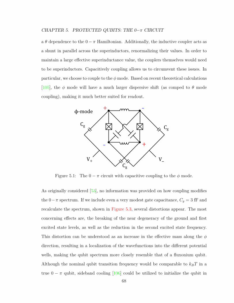
CHAPTER 5. PROTECTED QUBITS: THE 0−π CIRCUIT
a θ dependence to the 0− π Hamiltonian. Additionally, the inductive coupler acts as
a shunt in parallel across the superinductors, renormalizing their values. In order to
maintain a large effective superinductance value, the couplers themselves would need
to be superinductors. Capacitively coupling allows us to circumvent these issues. In
particular, we choose to couple to the φmode. Based on recent theoretical calculations
[105], the φ mode will have a much larger dispersive shift (as comped to θ mode
coupling), making it much better suited for readout.
ϕ-mode_+
+_
V+ V_
Cg Cg
Cg
Figure 5.1: The 0− π circuit with capacitive coupling to the φ mode.
As originally considered [53], no information was provided on how coupling modifies
the 0−π spectrum. If we include even a very modest gate capacitance, Cg = 3 fF and
recalculate the spectrum, shown in Figure 5.3, several distortions appear. The most
concerning effects are, the breaking of the near degeneracy of the ground and first
excited state levels, as well as the reduction in the second excited state frequency.
This distortion can be understood as an increase in the effective mass along the φ
direction, resulting in a localization of the wavefunctions into the different potential
wells, making the qubit spectrum more closely resemble that of a fluxonium qubit.
Although the nominal qubit transition frequency would be comparable to kBT in a
true 0 − π qubit, sideband cooling [106] could be utilized to initialize the qubit in68

CHAPTER 5. PROTECTED QUBITS: THE 0−π CIRCUIT
V- V+
1 2
3 4
Figure 5.2: The circuit layout for the most recent 0 − π design. The voltage nodeslabels are overlaid on the circuit, with the large red patterns indicating the Nb capac-itors. The blue boxes represent the CPS resonator coupling electrodes, with appro-priate capacitances indicated with dashed lines. The circuit topology is equivalent tothat shown in Figure 5.1.
its ground state, provided that the thermal occupation of the second excited state is
negligibly small. The approximation of a unoccupied second excited state will break
down as Cg is increased and a new scheme for qubit initialization will have to be
determined.
5.2 Soft 0−π regime
The original 0 − π target superinductance of ∼3 µH leads to an additional design
constraint. If a JJ array is used to build the superinductor, the self-resonant modes
of the array will set a hard limit on the number of junctions in the array. As was
found in [39], the mode frequencies of a JJ array are given by
ωk = ωp
√√√√√ 1− cos πkN
C02CJ +
(1− cos πk
N
) , (5.1)
69

CHAPTER 5. PROTECTED QUBITS: THE 0−π CIRCUIT
where ωp is the single junction plasma frequency, N is the number of junctions, CJ
is the individual junction capacitance, C0 is each junction’s parasitic ground capac-
itance, and k is the mode number. The array junction inductance needs to be kept
low, about 3 nH/junction to avoid dephasing from quantum coherent phase slips [52],
which implies an array length of ∼1000 junctions. For carefully constructed junctions
with a C0/CJ = 50 and typical values of ωp/2π = 20 GHz, the first junction array
mode would appear at 450 MHz, near and above which, the impedance of the superin-
ductor is no longer linear. Construction of such a large superinductor with kinetic
inductance materials involve fabricating wire lengths in excess of 5 mm (based on the
Lk values from the NSFQ experiments). Due to these challenges, we have chosen a
parameter regime dubbed the “soft” 0− π. The “soft” 0− π parameter set is chosen
such that EJ , ECJ > EC , EL by roughly one order of magnitude rather than the 2-3
orders in the original proposal. In this regime, the near degeneracy of the ground and
first excited state has been traded away for a reduction in the number of junctions,
and for a reduction in the size of the shunting capacitors between nodes 1-3 and 2-4.
A near degeneracy of a few hundred MHz can still be achieved near the half-flux
quantum sweet spot, which could be a promising spot to operate the qubit.
5.3 Fabrication
The design of the 0−π has gone through several iterations. In order to simultaneously
maintain a low EC and high ECJ , the distance between the positive and negative
nodes of the circuit is spatially large, ∼ 250 µm. This results in a very large flux
loop, leaving the circuit more susceptible to dephasing from 1/f flux noise. An early
design of the circuit had a gradiometric flux loop design [98] with wires crossing over a
SiN dielectric bridge, in order to reduce the size of the flux loop and the susceptibility
70

CHAPTER 5. PROTECTED QUBITS: THE 0−π CIRCUIT
0 /2
ext/ 0
0.0
0.5
1.0
1.5E
(GHz
)
0 /2
ext/ 0
0
2
4
6
8
E (G
Hz)
Figure 5.3: The transition frequencies for the first few eigenstates of a 0−π coupledwith Cg = 3 fF (left) and a soft 0− π (right). The circuit parameters for the spectraare EJ = 10 GHz, C = 520 fF, L = 4.075 µH, Cg = 3 fF, and ωp/2π = 40 GHz forthe 0 − π . The simulation parameters for the more experimentally accessible soft0− π are EJ = 6 GHz, C = 20 fF, L = 500 nH, Cg = 3 fF, and ωp/2π = 14 GHz.
to global flux noise. This design could be revisited in the future, however, presently,
the additional fabrication steps for dielectric sputtering and etching seemed to have
a detrimental effect on the device fabrication yield. Devices with both JJ arrays and
NbTiN nanowires have been fabricated in the hope to find the best-performing design.
The circuit layout must be modified from Figure 5.1 in order to avoid crossing
wires. The two nodes can be simultaneously coupled without wire crossings, as the
electric field from the coupling capacitor is not completely screened by the first metal-
lic wire as shown in Figure 5.2. The voltage pad dimensions are set to minimize the
asymmetry in the gate capacitance Cg between the lead and each of the circuit pads.
A coplanar strip-line (CPS) [82] λ/2 resonator is used to drive the 0−π circuit. This
requires the addition of a Krytar-4040124 180 hybrid coupler [78] to differentially
drive the resonator. Using a CPS resonator obviates the need for an on chip ground
71

CHAPTER 5. PROTECTED QUBITS: THE 0−π CIRCUIT
plane, which helps reduce the stray capacitance, keeping ECJ large. The hybrid cou-
pler has a limited frequency bandwidth, of 4-12 GHz, and so additional versions of the
0− π circuit have been fabricated and tested with a CPW resonator that terminates
in a CPW-CPS transition [107]. The circuit can be further twisted, see Figure 5.2 to
eliminate the crossing of the shunt capacitors in the middle of the circuit.
5.4 Spectroscopy
Several 0− π devices have been measured, and the data from one of the most recent
devices is presented here. This device is φ mode coupled to a CPS resonator with
JJ array superinductors. Using the measurement setup detailed in Chapter 3, we
perform two-tone spectroscopy. The resulting data are shown in Figure 5.5, along
with a corresponding theory fit overlay. The first plasmon and fluxon transitions
(white circles) are accompanied by several additional transitions. There are several
copies of the first fluxon transition (black circles), shifted higher in frequency by 2.2
and 4.4 GHz, corresponding exactly to the extracted frequency of the harmonic χ
mode at χ =√
8ELEC → 2.2 GHz. The visibility of these transitions indicates that
there is enough disorder in the different circuit elements to couple the χ mode to the
energy levels. In addition to the χ modes, there is a transition between the excited
plasmon and fluxon states, indicating a non-zero thermal population of the fluxon
excited state. The ratio of EJ/ECJ is sufficiently large that the sweet spot gap at
zero and half a flux quantum is closed, indicating that the fluxon transition will not
have a flux-insensitive sweet spot.
72

CHAPTER 5. PROTECTED QUBITS: THE 0−π CIRCUIT
-4 -2 0 2 4
0
-4 -2 0 2 4 -4 -2 0 2 4
Figure 5.4: The 0 − π wavefunctions near Φext = 0. The color maps indicate thesquare of the magnitude of the wavefunction, |Ψ|2, for the ground (left), first plas-mon (middle), and fluxon (right) excited states, with darker colors indicating smallerwavefunction magnitudes.
5.5 0−π lifetime measurements
Although the parameters of this implementation of the 0− π are not ideal for qubit
operation, we can still characterize a relaxation time of the circuit. This particu-
lar 0 − π device was recooled to characterize the excited state lifetimes. Using the
measurement setup outlined in Chapter 3, we apply Xπ pulses, resonant with the
first plasmon and fluxon transitions, and measure the excited state population as a
function of wait time to determine T1 as shown in Figure 5.6. As was the case in
the NSFQ devices, there is a significant enhancement in the lifetime of the fluxon
compared to the plasmon state which can be explained with the comparatively lower
matrix element, 〈0|ϕ|1〉 > 〈0|ϕ|2〉 (where the state |1〉 refers to the plasmon excited
state and |2〉 refers to the fluxon). At this flux, T2 < 200 ns and is expected to be
limited by flux noise as the fluxon transition has a linear flux dispersion.
Although this T1 is by no means a record value for superconducting qubits, there is
certainly room for design improvements. Working at lower fluxon frequencies should
help reduce capacitive loss, as well as increasing the qubit-measurement resonator
detuning (∆ = 2 GHz in this case). Future 0−π devices are currently being designed
73
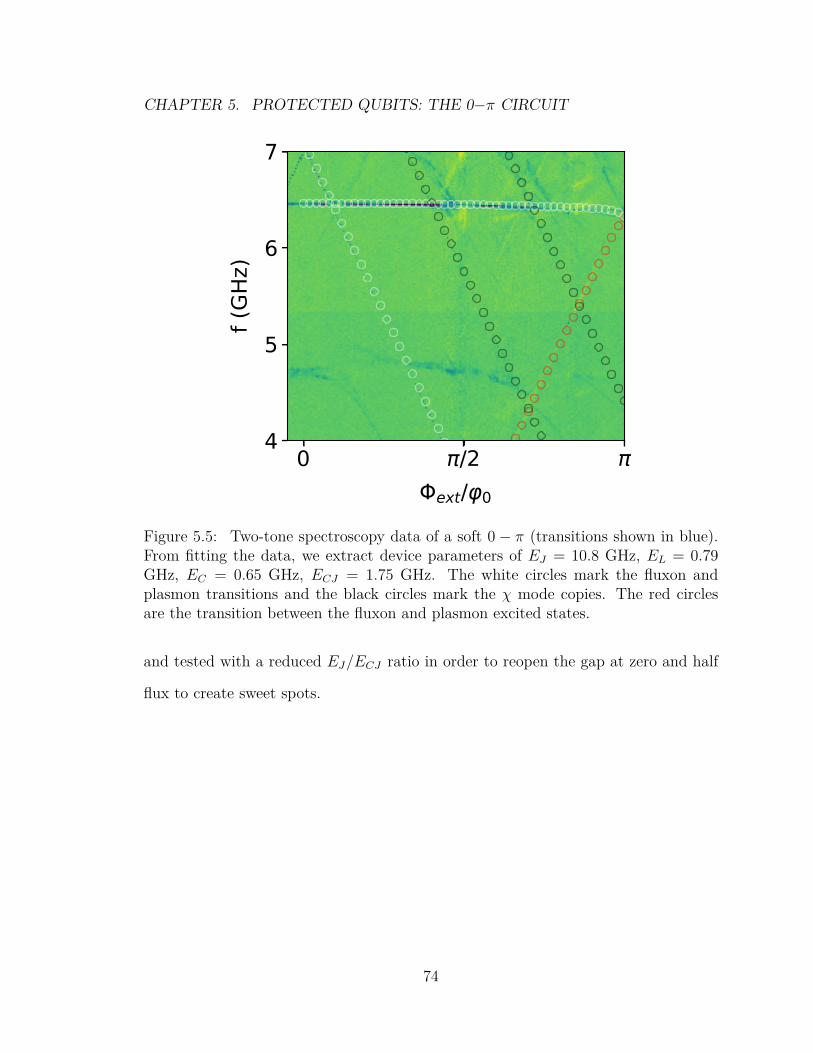
CHAPTER 5. PROTECTED QUBITS: THE 0−π CIRCUIT
0 /2ext/ 0
4
5
6
7
f (GH
z)
Figure 5.5: Two-tone spectroscopy data of a soft 0 − π (transitions shown in blue).From fitting the data, we extract device parameters of EJ = 10.8 GHz, EL = 0.79GHz, EC = 0.65 GHz, ECJ = 1.75 GHz. The white circles mark the fluxon andplasmon transitions and the black circles mark the χ mode copies. The red circlesare the transition between the fluxon and plasmon excited states.
and tested with a reduced EJ/ECJ ratio in order to reopen the gap at zero and half
flux to create sweet spots.
74

CHAPTER 5. PROTECTED QUBITS: THE 0−π CIRCUIT
0 5 10 15 20t ( s)
0.2
0.6
1.0
hom
odyn
e vo
lt. (a
rb.)
T1= 3.8 s
0 100 200 300t ( s)
0.2
0.6
1.0
T1= 82 s
Figure 5.6: The demodulated homodyne voltage from the measurement circuit as afunction of wait time, t. T1 is found from the exponential decay for the plasmon (left)and fluxon (right) states. These data were obtained near Φext = π/4, with a plasmonfrequency of ω/2π = 6.5 GHz and a fluxon frequency of ω/2π = 5.5 GHz.
75

Chapter 6
Elimination of Static Crosstalk
In superconducting qubits, the leading approaches for implementing two qubit gates
involve either fixed or tunable frequency qubits. Gates based on tunable qubits have
the advantage of being fast and having high on/off ratios [108]. By keeping a large
detuning between qubits when they are idle, the interaction strength can be greatly
suppressed. However, these features come at the price of having an increased sensi-
tivity to flux noise, as well as increasing the complexity of wiring and tuning up all
single and two qubit gates.
An alternative scheme uses fixed frequency qubits with linear coupling to achieve
a microwave activated two qubit gate [109]. This has the advantage of a simple
microwave setup, requiring no additional bias lines for the fast flux pulses, as well
as utilizing fixed frequency qubits which are insensitive to magnetic flux noise. A
simplified Hamiltonian of two driven qubits coupled with a linear element can be
written as
H/~ = ε1 (XI + (m12 − ν1)IX − µ1ZX −m12µ2XZ)
+ ε2 (IX + (m21 + ν2)XI + µ2XZ −m21µ1ZX)
+ ω1ZI/2 + ω2IZ/2− ζZZ/4,
(6.1)
76

CHAPTER 6. ELIMINATION OF STATIC CROSSTALK
where AB ≡ σA ⊗ σB, ε1(2) and ν1(2) are the strengths and frequencies of the two
drives, m12(21) are the spurious electromagnetic couplings between the qubits, and
µ1(2) = J/∆ is the interaction strength, J , divided by the qubit frequency detuning
∆ [110]. This Hamiltonian describes the so called “cross-resonance” gate [111] in
which the control qubit is driven at the target qubit’s frequency. The target qubit
will experience an X rotation based on the state of the control qubit. The additional
IX and XI terms represent the spurious electromagnetic crosstalk and the Stark shift
on the control qubit from the off resonant drive at the target frequency. The final
term in eqn. 6.1, ζZZ/4 describes a static, always on, quantum crosstalk between
the qubits. This term describes the constant rate of phase accumulation between
the two qubits which will lead to dephasing of the system. When multiple qubits
become entangled, keeping track of the ZZ terms between all pairs of qubits quickly
complicates any type of echo correction schemes. Additionally, this type of crosstalk
limits the fidelity of XX parity measurements that would be used in a surface code
quantum error correction scheme [112, 113]. Therefore eliminating the ZZ term in
the Hamiltonian would be a major improvement in the system.
6.1 ZZ crosstalk
The ZZ crosstalk arises from inclusion of the higher energy levels of the transmon
qubits. By including all energy terms up to fourth order, the strength of the ZZ
interaction for two transmons coupled by a bus cavity [114, 115] can be expressed as
ζ = 2g21g
22
[1
(∆12 + α2) ∆21
+ 1(∆21 + α1) ∆2
2+ 1
∆1∆22
+ 1∆2
1∆2
], (6.2)
where gi is the strength of the coupling between the ith transmon and the bus cavity,
∆i is the detuning between the ith transmon and the bus cavity, ∆12 is the frequency77

CHAPTER 6. ELIMINATION OF STATIC CROSSTALK
detuning between the qubits (with ∆21 = −∆12), and αi is the anharmonicity of the
ith transmon. More intuitively, the ZZ interaction arises from the frequency shift of
the system when one of the qubits is in it’s excited state,
ζ = ω11 − ω01 − ω10. (6.3)
This intuitive picture is suggestive, as it alludes to a method of measuring the ζ with
a cross-Ramsey experiment, described in Section 6.3.
A novel method for canceling ζ is to use a second coupling element to destructively
interfere the ζ terms arising from each coupler. The Hamiltonian describing such a
system is given by,
H/~ =∑
i=1,2,±
(ωia†iai −
αi2 a†ia†iaiai
)+∑j=±
∑i=1,2
gij(a†iaj + aia
†j
), (6.4)
where the subscripts 1, 2,± denote each of the transmons and couplers, with ωi, αi,
and gij as the frequencies, anharmonicities, and couplings of the ith object (only
including g1,± and g2,±). By numerically diagonalizing eqn. 6.4, we can extract the
strength of ζ as a function of the qubit and resonator couplings, detunings, and
anharmonicities [115]. In particular, the set of parameters for which ζ = 0 occurs
when ∆12 < α1, α2 and ω− < ω1, ω2 < ω+. In theory, all components could be
frequency tunable, but for coherence purposes, fixed frequency transmons are optimal,
and only one coupler frequency needs to be tuned to achieve ζ = 0. As fabrication
processes are improved, reducing the spread in EJ (and therefore ωi), one could
imagine having both couplers fixed in frequency, eliminating the need for any on-chip
flux bias lines.
78

CHAPTER 6. ELIMINATION OF STATIC CROSSTALK
6.2 Improved device design
The first generation of zero-ZZ devices [115] had several design parameters to be
improved, first among them, the ratio of EJ/EC . While working in the straddling
regime, when the two transmon frequencies sitting between the two coupler frequen-
cies, the appropriate choice of the remaining device parameters is key. In the first
iteration of the zero ZZ device, one of the main design considerations was keeping the
qubits and couplers well below the readout resonator frequency. Additionally, given
the variations in EJ at the time of fabrication of the first device, the designed EC was
around -400 MHz, to increase the yield of devices without frequency collisions (eg.
ω1 = ω2 − α2). Having a large EC also has the added benefit of reducing leakage out
of the computational subspace. The readout resonator frequency, generally speaking,
should be as high as practically possible to eliminate thermal occupation of photons
in the cavity which lead to qubit dephasing [75]. “Practical” has several different
considerations including maintaining a reasonable dispersive shift, χ, so that high
fidelity readout can be achieved, and placing the resonators in the frequency band of
low noise amplifiers (HEMTs, JPCs, TWPAs). This currently sets the upper limit at
around 8 GHz. The first device was designed to have qubits detuned from the readout
resonator by about 3 GHz which puts the qubits at 5 GHz. When calculating the EJ
for a fixed EC and ω/2π = 5 GHz, we find
ω01/2π =√
8EJEC − EC ⇒ EJ = 9.1 GHz, (6.5)
79

CHAPTER 6. ELIMINATION OF STATIC CROSSTALK
which gives a ratio of EJ/EC ≈ 23. When we consider the charge dispersion of such
a system (eqn. 2.16)
ε1 = 29EC
√2π
(EJ
2EC
)5/4e−√
8EJ/EC ⇒ ε1 ≈ 1 MHz. (6.6)
With the given EJ/EC and ε1, the transmons are approaching the Cooper-pair box
regime, and the first version of the zero ZZ devices suffered from short Tϕ due to
charge noise. In addition to the large susceptibility to charge noise, the frequency
for the lower coupler at the ζ = 0 point was ω− ≈ 4 GHz. With an effective cavity
temperature of about 90 mK, this severely limited the iSWAP gate fidelity to <
85%. As the lower coupler is formed with what amounts to a tunable transmon, a
SQUID loop with large capacitance, this gives an even lower EJ/EC than the qubits.
Although thermal occupation could potentially be addressed with better filtering and
attenuation on the flux line, a better solution, solving both the charge dispersion
and thermal issues, involves moving the qubits and couplers higher in frequency.
Frequency crowding and relaxation could set an upper bound on how close the qubits
can be moved to the readout resonators, however, future designs could incorporate a
Purcell filter [79, 116] allowing for smaller detunings between the readout resonators
and qubits.
With these considerations, we fabricate a second device with the parameters in
Table 6.1. The primary considerations included both reaching EJ/EC = 50 and
increasing gij between each of the couplers and the qubits. Traditionally, the coupling
strength has been set as a tradeoff between maintaining large qubit-qubit interaction,
J , and minimizing crosstalk between the qubits. With fixed linear couplers, there
is a fundamental tension that comes from the fact that the strength of J and ζ are
both proportional to the coupling. With the two coupler design, we can now consider
80

CHAPTER 6. ELIMINATION OF STATIC CROSSTALK
increasing gij for each qubit, while ζ can be nulled out with the tunable coupler.
Minor additional changes include decreasing EC and making asymmetric junctions
in the coupler to reduce the flux sensitivity [117]. To have some estimate before
Parameter Symbol ValueQ1 frequency ω1/2π 6.143 GHz
Q1 anharmonicity α1/2π 330 MHzQ1 relaxation time T
(1)1 12.5 µs
Q1 coherence time T(1)2E 22.5 µs
Q2 frequency ω1/2π 6.427 GHzQ2 anharmonicity α1/2π 330 MHzQ2 relaxation time T
(1)1 7.0 µs
Q2 coherence time T(1)2E 9.3 µs
Bus cavity frequency ω+/2π 7.073 GHzMaximum coupler frequency ωmax− /2π 7.19 GHz
Coupler anharmonicity α−/2π 290 MHzQ1-bus coupling g1+/2π 102 MHzQ2-bus coupling g2+/2π 102 MHz
Q1-tunable coupler coupling g1−/2π 85 MHzQ2-tunable coupler coupling g2−/2π 85 MHz
Table 6.1: Parameters for improved zero ZZ device.
fabricating the devices, we simulated the device design in Maxwell 3D Electrostatic
solver, the details of which are in Appendix. B. This gives us a rough estimate for the
capacitances of the device, from which, we can write a circuit model to calculate the β
for each coupler/resonator and EC for the qubits and couplers. Based on the two-tone
spectroscopy measurements, the simulated EC ’s are within 5% of the experimentally
measured values.
6.2.1 Device fabrication
We provide a high level summary of the device fabrication, with the fabrication
details listed in Appendix. A. A single photolithography step was performed to pat-
81
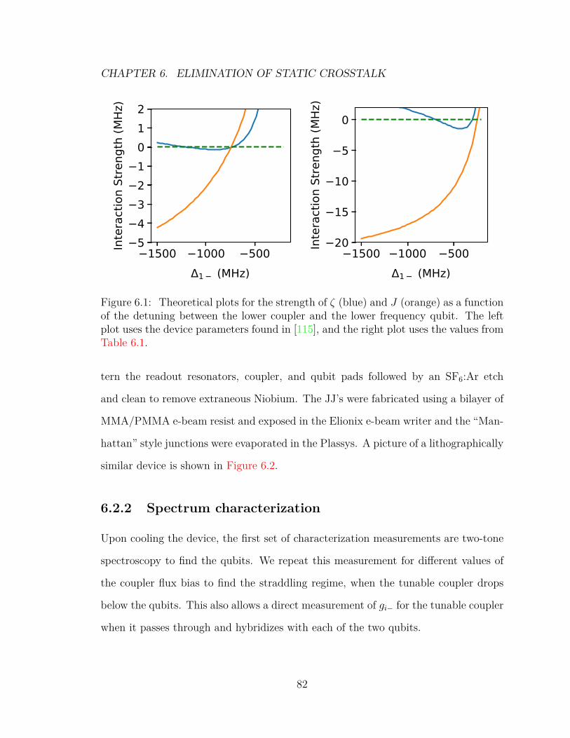
CHAPTER 6. ELIMINATION OF STATIC CROSSTALK
1500 1000 5001 (MHz)
54321012
Inte
ract
ion
Stre
ngth
(MHz
)
1500 1000 5001 (MHz)
20
15
10
5
0
Inte
ract
ion
Stre
ngth
(MHz
)Figure 6.1: Theoretical plots for the strength of ζ (blue) and J (orange) as a functionof the detuning between the lower coupler and the lower frequency qubit. The leftplot uses the device parameters found in [115], and the right plot uses the values fromTable 6.1.
tern the readout resonators, coupler, and qubit pads followed by an SF6:Ar etch
and clean to remove extraneous Niobium. The JJ’s were fabricated using a bilayer of
MMA/PMMA e-beam resist and exposed in the Elionix e-beam writer and the “Man-
hattan” style junctions were evaporated in the Plassys. A picture of a lithographically
similar device is shown in Figure 6.2.
6.2.2 Spectrum characterization
Upon cooling the device, the first set of characterization measurements are two-tone
spectroscopy to find the qubits. We repeat this measurement for different values of
the coupler flux bias to find the straddling regime, when the tunable coupler drops
below the qubits. This also allows a direct measurement of gi− for the tunable coupler
when it passes through and hybridizes with each of the two qubits.
82

CHAPTER 6. ELIMINATION OF STATIC CROSSTALK
Q1
Q2
ω+
ω_
Bias line
readout
readout 500 μm
Figure 6.2: An optical image of the zero ZZ device. The two transmons arehighlighted in blue, the tunable coupler in red, the fixed frequency coupler ingreen(connected outside image), and the coupler bias line in purple. The readoutresonator leads for each qubit extend beyond the top and bottom of the image.
5.9 6.0 6.1 6.2 6.3 6.4 6.5 6.6fspec (GHz)
0.4
0.6
0.8
1.0
1.2
Flux
bia
s (V)
40
30
20
10
0
S 21 (
dB)
Figure 6.3: Two-tone spectroscopy data near the crossing of the qubit and the tunablecoupler. From the hybridization of the qubit and coupler energy levels, we extract ag1,2−/2π = 85 MHz.
83
CHAPTER 6. ELIMINATION OF STATIC CROSSTALK
6.3 ZZ crosstalk map
Once the flux bias is set such that the tunable coupler is below the two qubits, we can
begin to characterize the strength of the ZZ interaction. As previously alluded to,
the magnitude of ζ is related to the frequency shift of one qubit based on the state of
the second qubit. We can perform a Ramsey pulse sequence, consisting of two Xπ/2
pulses separated by a wait time, to measure the frequency of one qubit (target), and
then repeat the sequence with an additional Xπ pulse on the other qubit (control)
before and after the Ramsey interferometric pulses to extract the difference frequency
when the control is its ground or excited state. By repeating the measurement with
the roles of the target and control qubits reversed, we can then extract the strength
of the ZZ interaction. We repeat the cross Ramsey experiment as a function of the
lower coupler frequency to find the point, or points, where ζ = 0. We also note that
having two solutions for ζ = 0 is not universal, and for different parameter sets there
can either be one or no solutions.
6.4 Single qubit gate tuneup
Once the zero ZZ points are found, the flux bias is fixed to the point with higher J
(see Figure 6.1). We perform several single qubit calibrations on each qubit, which
include frequency calibration, amplitude for each of the pulses (Xπ,±π/2 and Yπ,±π/2),
and correcting the azimuthal angle between the two quadratures coming from the
generator [118]. All pulses are generated with a vector signal generator set at the
qubit frequency and gated with a Gaussian shape pulse with a width of σ = 8 ns
generated with an arbitrary waveform generator (AWG). Calibration of the pulse
amplitudes can be performed by applying a single π/2 pulse and then a sequence of n,
84

CHAPTER 6. ELIMINATION OF STATIC CROSSTALK
0.95 1.00 1.05 1.10 1.15 1.20 1.25 1.30 1.35Flux bias (V)
0.25
0.00
0.25
0.50
0.75
1.00
1.25 (M
Hz)
Figure 6.4: ζ plotted vs. coupler flux bias. ζ is obtained via a cross-Ramsey mea-surement, as described in the text. ω− is decreasing with increasing flux bias. Theζ = 0 point at 1.11 V is used for all iSWAP and CR measurements.
π or π/2 pulses around either the X or Y axis and then measuring the Z projection. If
the pulses have the correct amplitude, then the qubit state will remain on the equator
of the Bloch sphere and have equal probability of a Z projection of |0〉 or |1〉. If there
is a slight amplitude error causing under/over rotation, the state will move off the
equator causing an imbalance in average measured state. This under/over rotation
can then be fixed by adjusting the amplitude of the modulating Gaussian pulse from
the AWG. A DRAG calibration [119] is also performed to reduce leakage into the
second transmon level with the addition of a Gaussian derivative shaped pulse in the
Q quadrature of the vector generator. Once the calibrations have been performed,
measurements of all combinations of two sequential I,Xπ, X±π/2, Yπ, Y±π/2 pulses are
performed in an “AllXY” [87] measurement (shown in Figure 6.5). This combination
of gates ideally leaves the qubit at the north pole, equator, or south pole of the Bloch
sphere. Deviations from these points generally indicate mis-calibrations of the single
85

CHAPTER 6. ELIMINATION OF STATIC CROSSTALK
IdId
XX
YY
XY
XX
YY
XY
YX
YY
XX
X/2
X/2
Y/2
Y/2
X/2
IdY
/2Id
X/2
IdY
/2Id
X/2
Y/2
Y/2
X/2
X/2
YY
/2X
X/2
XX
X/2
Y/2
YY
Y/2
X/2
Y/2
Y/2
X/2
X/2
YY
/2X
X/2
XX
X/2
Y/2
YY
Y/2
XId
YId
XId
YId
X/2
X/2
Y/2
Y/2
X/2
X/2
Y/2
Y/2
0.0
0.2
0.4
0.6
0.8
1.0P(
|1)
Figure 6.5: Z projection for AllXY measurements of Q1 at 1.11 V flux bias afterperforming amplitude and phase calibrations of all combinations of cardinal X and Yrotations. Q2 is left idle during these measurements.
qubit gate pulses and the calibration procedures can be rerun to iteratively reduce
the deviation from the ideal AllXY values.
6.5 Single qubit randomized benchmarking
Randomized benchmarking (RB) is an efficient tool to characterize qubit performance
and is insensitive to so called state preparation and measurement (SPAM) errors
making it an easy to implement in a wide variety of systems [120]. We take the set of
24 single qubit Clifford gates, choose 20 sequences of a random ordering of n gates,
and repeat each sequence ∼ 103 times. At the end of the sequence a final “undo”
Clifford [121] gate brings the system back into an eigenstate of Z, and the qubit is
measured. The RB sequence acts as a depolarizing channel for the qubit [28] and for
very long sequence lengths, a qubit should have P |0〉 = 0.5 indicating that it is a fully
mixed state. The curves are fit to a function of the form P |0〉 = A(1−2r)n+B [122],
86
CHAPTER 6. ELIMINATION OF STATIC CROSSTALK
where A and B are constants associated with the state preparation and measurement,
n is the number of gates, and r is the error per gate which can further be divided by
the average number of Cliffords per gate. In our decomposition, the average number
of Cliffords per gate is 1.875 [115]. To characterize our system, we can perform RB in
two different ways, individually and simultaneously. For two qubit systems, the set
of Clifford gates grows to 11,520 [122, 123] which presents a challenge to efficiently
detect correlated errors between the two qubits. Recent investigations have shown
that the full set of two qubit Cliffords does not have to be investigated and that
useful information about the system can be extracted by performing single qubit RB
on each subsystem (qubit) simultaneously [124]. Simultaneous RB will give us an
additional measurement of the system crosstalk. The ZZ interaction has the effect
of shifting one of the qubit frequencies based on the state of the other, and if there
is crosstalk present between the two qubits, performing gates, such as Xπ will excite
one qubit causing a Stark shifted energy of the second qubit. If this occurs while a
pulse is applied to the second qubit, that pulse will now be off resonant causing a
“misrotation”. When we compare the results of simultaneous and individual RB for
the two qubits at the ζ = 0 point in Figure 6.6, we see that the error per Clifford is
the same between the individual and simultaneous RB experiments, with a measured
error that is consistent with the lifetime and coherence of the individual qubits. This
measurement is an additional confirmation that the ZZ crosstalk has been removed
from the system.
6.6 iSWAP gate
A parametric two qubit drive can be activated when the coupling strength between
two qubits is modulated at the frequency difference between the qubits [125–129].
87

CHAPTER 6. ELIMINATION OF STATIC CROSSTALK
0 100 200 300 400 500 600 700 800Num. of gates
0.5
0.6
0.7
0.8
0.9
1.0P 0
Q1 ind.Q2 ind.Q1 sim.Q2 sim.
Figure 6.6: Individual and simultaneous randomized benchmarking at the ζ = 0point. The extracted error per Clifford gate is 4.75×10⁻³ for Q1 and 1.25×10⁻² forQ2 where the lower fidelity in Q2 is due to the shorter coherence time. The error pergate for simultaneous RB is within the measurement uncertainty of the individualRB error for each qubit.
Following the description in [130], the two qubit interaction is given by
Uint =
1 0 0 0
0 cos (gt/2 + φ) −i sin (gt/2 + φ) 0
0 −i sin (gt/2 + φ) cos (gt/2 + φ) 0
0 0 0 1
, (6.7)
where g is the interaction strength and φ is the azimuthal angle of the microwave
generator controlling the flux pulse. When the interaction is left on for a time gt = π,
the input state |01〉 is changed to i|10〉 known as an iSWAP gate, which, with the
addition of single qubit gates, can be used to perform a CNOT gate. Although each
of the qubits in the device are single junction transmons and should nominally have a
fixed frequency, interaction with the tunable coupler effectively dresses the qubits and
will cause a small shift in qubit frequency as the tunable coupler is adjusted, allowing
88

CHAPTER 6. ELIMINATION OF STATIC CROSSTALK
0 200 400Drive Time (ns)
265
270
275
280
285
/2 (M
Hz)
Q1
0 200 400Drive Time (ns)
265
270
275
280
285
/2 (M
Hz)
Q2
0.2
0.4
0.6
0.8
1.0
P 1(Q
1)
0.2
0.4
0.6
0.8
P 1(Q
2)
Figure 6.7: Rabi oscillations between the states |10〉 and |01〉 following an Xπ pulseon Q1 as a function of coupler drive time and drive frequency. The two plots are thereadout from Q1 (left) and Q2 (right). No oscillations are present in the first ∼ 15 nsdue to the Gaussian rising edge of the coupler drive pulse.
us to perform a two qubit iSWAP gate. We can probe this interaction by applying
a sinusoidal drive near ∆12 for varying lengths of time. A Xπ pulse is first applied
to Q1, putting the system into the state |10〉 before the coupler drive is turned on.
The coupler pulse consists of a sinusoidal drive modulated with a rectangular pulse
having 3σ (with σ = 5 ns) rising and falling Gaussian edges. Figure 6.7 shows the Z
projection of the qubit states. There is a slight difference in the maximum Chevron
swap frequency and ∆12 due to the ac Stark shift arising from the coupler drive pulse
[131].
6.6.1 Quantum state tomography
To characterize the fidelity of our iSWAP gate we use quantum state tomography
(QST) to prepare a specific quantum state and determine the distance to the ideal
state [28]. Before performing QST, the system is calibrated to individually readout
the state of each qubit after a single pulse sequence. To do this, the phase of the local
oscillator (LO) for each measurement resonator is rotated to move the demodulated
89

CHAPTER 6. ELIMINATION OF STATIC CROSSTALK
homodyne readout signal from each qubit into a single field quadrature. For each
qubit, we apply either an Xπ or I pulse before measurement for ∼ 104 trials and
histrogram the results to generate a readout matrix, Ci, which characterizes how often
the correct state is identified [129] for the ith qubit. We also perform a “crosstalk
calibration” measurement, which prepares the states |00〉, |10〉, |01〉, and |11〉 and
measure the 4x4 matrix, Cct, corresponding to the prepared vs. measured two qubit
state. The corrected state is given by
pcorr = R−1pmeas, (6.8)
with
R = Cct · (CI ⊗ CII) . (6.9)
An example of the readout corrected single shot data for a coupler pulse is shown in
Figure 6.8.
Written in the Pauli basis form [28], the density matrix can be expressed as
ρ = 12n
16∑i
tr (Piρ)Pi, (6.10)
where n = 2 for a two qubit system and the sum runs over 15 independent measure-
ment correlators Pi ∈ I,X, Y, Z⊗2 − II. In this set, six correlators are “single
qubit like”, that is are equivalent to 〈M1I〉 or 〈IM2〉, and the remaining nine are
the two qubit correlators, 〈M1M2〉. Experimentally, we measure three independent
probabilities, P00, P10, and P01 (with P11=1-P00-P10-P01), and we can express these
90

CHAPTER 6. ELIMINATION OF STATIC CROSSTALK
0 200 400 600 800 1000 1200 1400Drive Time (ns)
0.0
0.2
0.4
0.6
0.8
1.0Po
pula
tion
P10P01
Figure 6.8: Readout corrected, single shot trace of the two qubit state vs. couplerdrive time. Note the drive power is higher than what is used in Figure 6.7. A drivetime of t = 105 ns corresponds to a
√iSWAP gate and t = 210 ns, a full iSWAP.
correlators as the following
〈M1I〉 =P11 + P10 − P01 − P00
〈IM2〉 =P11 + P01 − P10 − P00
〈M1M2〉 =P11 + P00 − P01 − P10.
(6.11)
To perform tomography, we apply certain gates prior to readout to rotate the mea-
surement basis, explicitly, Y−π/2 for Pauli X and Xπ/2 for Pauli Y, and I for Pauli Z.
Once the readout correction matrices (eqn. 6.9) have been measured, we can prepare a
specific state, in this case an Xπ is applied to Q1 followed by 105 ns long coupler drive,
which should give a√
iSWAP gate based on the measurements in Figure 6.8. This
sequence produces the maximally entangled state |Ψ〉 = 1/√
2 (|10〉+ i|01〉). The
91

CHAPTER 6. ELIMINATION OF STATIC CROSSTALK
tomographic readout of this state is shown in the top panel of Figure 6.9 compared to
the theoretically predicted state. Due to noise and other systematic readout errors,
the measured density matrix may be unphysical, eg. have negative eigenvalues, and
the raw density matrix is fit to obtain the closest physical density matrix [132]. This
is then compared to the ideal theoretical density matrix to obtain a state fidelity of
99.47%. The concurrence [28], is defined as
C (ρ) ≡ max (0, λ1 − λ2 − λ3 − λ4) , (6.12)
where λi are the sorted eigenvalues of the density matrix. From the fit density matrix,
we extract maximum concurrence of C = 0.985 for the prepared state.
6.7 Cross-resonance gate
As an alternative to modulating the coupler bias voltage, one of the qubits can be
driven at the second qubit’s frequency to perform a cross-resonance (CR) two qubit
gate. As recently explored theoretically [133], the strength of the two qubit interac-
tion, µ, in the Hamiltonian eqn. 6.1, to third order, can be expressed as
µ = − JΩ∆12
(α1
α1 + ∆12
)+ JΩ3α2
1 (3α31 + 11α2
1∆12 + 15α1∆212 + 9∆3
12)4∆3
12 (α1 + ∆12)3 (α1 + 2∆12) (3α1 + 2∆12), (6.13)
where J is the interaction strength, Ω the drive strength, α1 the anharmonicity of the
control qubit, and ∆12 the qubit frequency detuning. Working at the ζ = 0 point, we
use Q1 as the control qubit and Q2 as the target qubit and apply the CR drive. As
the ZX rotation depends on the state of Q1, we perform the experiment twice, once
with an Xπ pulse on Q1 before the CR drive, and once without the pulse (with Q1
92
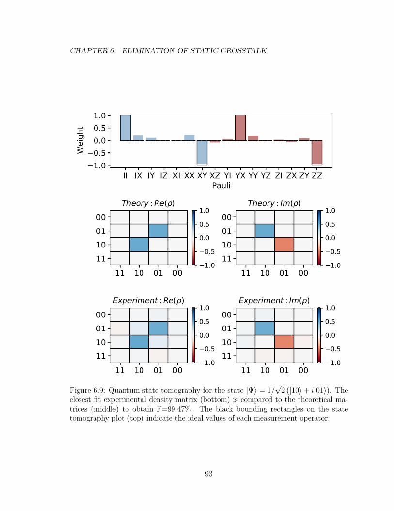
CHAPTER 6. ELIMINATION OF STATIC CROSSTALK
II IX IY IZ XI XX XY XZ YI YX YY YZ ZI ZX ZY ZZPauli
1.00.50.00.51.0
Wei
ght
11 10 01 0011100100
Theory : Re( )
11 10 01 0011100100
Theory : Im( )
11 10 01 0011100100
Experiment : Re( )
11 10 01 0011100100
Experiment : Im( )
1.0
0.5
0.0
0.5
1.0
1.0
0.5
0.0
0.5
1.0
1.0
0.5
0.0
0.5
1.0
1.0
0.5
0.0
0.5
1.0
Figure 6.9: Quantum state tomography for the state |Ψ〉 = 1/√
2 (|10〉+ i|01〉). Theclosest fit experimental density matrix (bottom) is compared to the theoretical ma-trices (middle) to obtain F=99.47%. The black bounding rectangles on the statetomography plot (top) indicate the ideal values of each measurement operator.
93
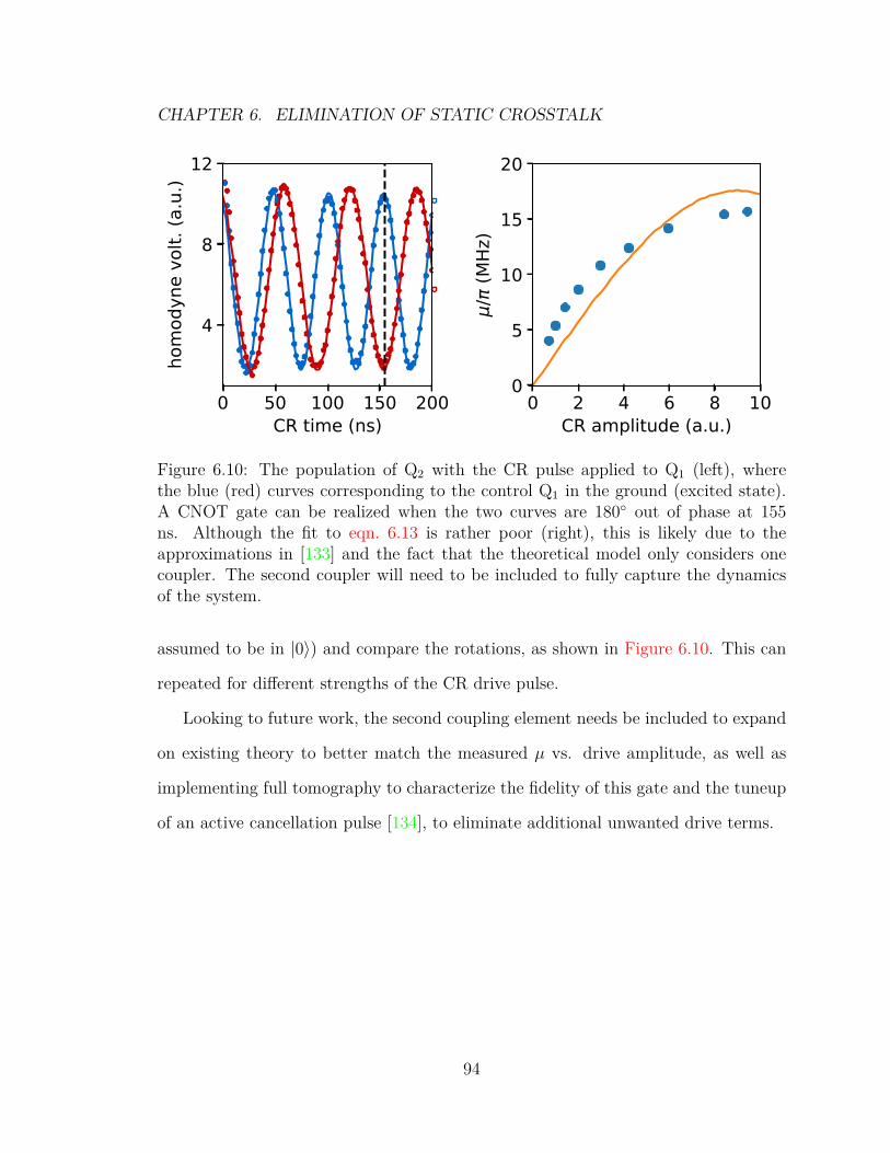
CHAPTER 6. ELIMINATION OF STATIC CROSSTALK
0 50 100 150 200CR time (ns)
4
8
12ho
mod
yne
volt.
(a.u
.)
0 2 4 6 8 10CR amplitude (a.u.)
0
5
10
15
20
/ (M
Hz)
Figure 6.10: The population of Q2 with the CR pulse applied to Q1 (left), wherethe blue (red) curves corresponding to the control Q1 in the ground (excited state).A CNOT gate can be realized when the two curves are 180 out of phase at 155ns. Although the fit to eqn. 6.13 is rather poor (right), this is likely due to theapproximations in [133] and the fact that the theoretical model only considers onecoupler. The second coupler will need to be included to fully capture the dynamicsof the system.
assumed to be in |0〉) and compare the rotations, as shown in Figure 6.10. This can
repeated for different strengths of the CR drive pulse.
Looking to future work, the second coupling element needs be included to expand
on existing theory to better match the measured µ vs. drive amplitude, as well as
implementing full tomography to characterize the fidelity of this gate and the tuneup
of an active cancellation pulse [134], to eliminate additional unwanted drive terms.
94
Chapter 7
Conclusion and Outlook
In this thesis, we have explored new materials for constructing superconducting
qubits, new circuit designs for qubits, and a method for elimination of crosstalk
in two qubit gates.
We have fabricated and measured a NbTiN based nanowire superinductance flux-
onium qubit, with a qubit lifetime of up to T1 = 20 µs. The qubit lifetime is limited
by inductive losses at qubit frequencies below 3 GHz. The presence of standing wave
modes in the nanowire modify the fluxonium spectrum and are visible above 16 GHz.
As the modes of the nanowire strongly depend on the parasitic and stray capaci-
tances of the wire, using a shorter wire with higher sheet inductance (for example
high quality granular aluminum films with one hundred times larger Lk = 2 nH/
[69, 90]), or integrating the fluxonium into a 3D cavity or waveguide [98], could re-
duce unwanted capacitances and help to push the nanowire self-resonant modes to
higher frequencies. Understanding the origin of the inductive loss is next on the list of
short term experiments to be performed on the nanowire fluxonium. Several poten-
tial sources of loss are the contact between the Al Josephson junction layers, residue
or debris on the surface of the nanowire, non-equilibrium quasiparticles breaking the
superconductivity in small localized regions of the wire, and some intrinsic loss source
95

CHAPTER 7. CONCLUSION AND OUTLOOK
associated with the NbTiN wire itself. Although previously observed in granular Al
nanowires [42], the large superconducting gap in NbTiN makes it unlikely that quasi-
particle poisoning is the main source of loss in the wire. The most likely culprit is
the NbTiN/ Al contact. This could be checked by changing the contact area between
the two layers, as well as changing the fabrication recipe related to making this con-
tact. Additionally, different wires could be fabricated with different aspect ratios, in
particular making a very thin and wide wire for maximal surface area, to determine
if the nanowire loss is related to this interface. An alternative set of investigations
could be performed making fluxonium devices with different LK materials as well. If
an appropriate material is found, with a sufficiently large coherence length, ξ, it is
conceivable to make an entire fluxonium device from a single fabrication layer, mak-
ing the long inductive nanowire thinner than ξ for a short length to form a weak-link
junction in series with the inductive wire.
We have started the experimental exploration of the Kitaev 0 − π [53] qubit
by fabricating and measuring devices which are in the so called soft 0 − π regime,
finding a qubit lifetime of T1 = 80 µs. Although the soft 0 − π regime is currently
accessible, there are several non-ideal features, which need to be addressed in future
experiments. Maintaining a small ECθ simultaneous to a large ECφ pushes the limits
of what can be reliably fabricated. Maintaining a large ECφ is critical to having a flux
intensive sweet spot, however this may be moving us into a regime where the qubit
has a large charge dispersion and is no longer insensitive to charge noise. The only
solution may be a continued efforts and improvements in the device fabrication to
reach the true 0−π limit which supports disjoint, nearly degenerate states which are
insensitive to charge noise. One additional challenge that needs further exploration
is the implementation of gates between the disjoint levels of the qubit to build up a
universal gate set, although recent theoretical work along this front has been recently
96
CHAPTER 7. CONCLUSION AND OUTLOOK
pursed [105] with promising results. While its not clear that the 0−π will become the
eventual replacement to the transmon, the concept of disjoint wavefunctions and near
degenerate eigenstates are features of multi-node circuits that will very likely lead to
a few order of magnitude increase in the lifetime and coherence of superconducting
qubits.
We have additionally fabricated, measured, and demonstrated a two qubit cou-
pling architecture which eliminates the ZZ type of parasitic qubit coupling. The
immediate follow up experiment would be to measure a three qubit device and verify
that the ZZ crosstalk can be simultaneously eliminated between all qubits. For com-
pleteness, this would be a demonstration that “spectator-qubit” errors [112] can be
eliminated, opening the door for near term quantum error correction. Improvements
to the device design include adding Purcell filters [79, 116] to the readout resonators
as well as the flux bias line on the coupler. As fabrication improvements continue to
reduce the fabrication spread in EJ , it also is conceivable to make devices with two
fixed frequency couplers and perform all two qubit gates with a cross-resonance gate,
eliminating the need for on chip flux bias.
In the past two decades, we have seen tremendous progress in superconducting
qubit lifetimes and coherences as well as an increased understanding in the physics of
cQED. Although it’s not clear which system will ultimately realize a significant ad-
vance over conventional computation, the steady progress in superconducting qubits
continues to keep the field rich with many new avenues of research to explore for the
future generation of Quantum Engineers.
97

Appendix A
Fabrication Recipes
A.1 NSFQ and nanowire 0− π process flow
• NbTiN sputtering on Sapphire (performed by StarCryo).
• Photolithography to protect NbTiN in select regions of device for nanowire
patterning and etch NbTiN in unprotected regions.
• Photolithography to cover NbTiN and sputter Nb.
• Photolithography for readout resonators and etch Nb.
• E-beam lithography for nanowire and etch NbTiN.
• Anti-charge layer for Josephson junctions and e-beam lithography for junctions.
A.2 Zero ZZ process flow
• Sputter Nb.
• Photolithography for readout resonators and etch Nb.
• Anti-charge layer for Josephson junctions and e-beam lithography for junctions.98

APPENDIX A. FABRICATION RECIPES
• Dicing into 7 x 7 mm chips is usually done after anti-charge layer and before
e-beaming the junctions but could be performed before anti-charge if there is a
concern of resist aging.
A.3 Niobium preparation
This is the new recipe using TAMI (Toluene, Acetone, Methanol, Isopropanol) clean-
ing before sputtering Nb in the AJA tool. As of the time of writing this recipe gives
consistent T1 times of ≈ 35 µs for single junction planar transmons, as well as sin-
gle photon Q’s above 1 million. C-plane (0001) sapphire substrates with 500 µm
thickness are purchased from CrysTec GmbH.
Substrate TAMI Cleaning
• Clean glass beakers (in order) with Acetone, Methanol and Isopropanol by
spraying each beaker and dumping waste rinse twice.
• Sonicate wafer in Toluene for 2 minutes. Remove from Toluene while spraying
wafer with Acetone to prevent drying and place into beaker with Acetone.
• Sonicate wafer in Acetone for 2 minutes. Remove from Acetone while spraying
wafer with Methanol to prevent drying and place into beaker with Methanol.
• Sonicate wafer in Methanol for 2 minutes. Remove from Methanol while spray-
ing wafer with IPA to prevent drying and place into beaker with Isopropanol.
• Sonicate wafer in Isopropanol for 2 minutes. Remove from Isopropanol with
one final spray rinse over beaker and blow dry with nitrogen.
99

APPENDIX A. FABRICATION RECIPES
Sputtering
• For 100 mm (4”) wafers, clamp the edges of the wafer onto the aluminum chuck
(or Nb sputtering chuck for smaller substrates) from AJA tool, blow off dust
from the wafer and load into AJA loadlock, and transfer wafer to main chamber
when the appropriate vacuum has been reached.
• Run recipe TH sputter Nb 200nm 12mTorr 90s delay, which heats sub-
strate to 200 for 10 minutes, allows the substrate to cool for 10 min-
utes, and sputters 200 nm of Nb onto the substrate. Non-heated recipe is
JS sputter Nb 200nm 12mTorr 90s delay.
Dicing
• Prep the wafer for dicing by spinning S1818 or equivalent as a protection layer.
Add resist and spin at speed of 4000 RPM for 60 seconds with a ramp rate of
10,000 RPM/s. Bake on center of hotplate at 115 for 1 minute.
• Place a tape ring on tape dispenser and place substrate with protective resist
face down. Carefully roll dicing tape over ring and substrate to avoid trapped
air bubbles, cut away excess tape and load into ADT dicing saw.
• Dice wafer with appropriate recipe.
• Place diced substrate into UV lamp to reduce tackiness of dicing tape.
100

APPENDIX A. FABRICATION RECIPES
A.4 Photolithography
Clean and spin coat
• If the chip has photoresist from previous lithography/etching/dicing steps, clean
chip in N-Methyl-pyrrolidone (different trade names NanoTM Remover PG, 1165
or MICROPOSITTM REMOVER 1165) heated to 80 for > 30 minutes.
• Spray clean with Isopropanol and blow dry with nitrogen
• Repeat TAMI cleaning steps.
• Spin S1811 at speed of 5500 RPM for 60 seconds, with a ramp rate of 10,000
RPM/s. Bake on center of hotplate at 115 for 1 minute.
• Optional: Briefly inspect substrate for resist bubbles or debris with UV filtered
microscope.
Exposure and development
Use Heidelberg DWL 66+ (Jadwin) for direct writing on chip. For sapphire sub-
strates, there must be metal on the substrate to use optical focus. If some metal has
been etched in previous lithography steps, start with pneumatic focus before finding
a region of the substrate with Nb and using optical focus. Standard exposure time
for 25 mm chip is ∼17 minutes.
• 5 mm write head: Focus = −76, filter 10 %, intensity 90 % - 95 %.
• Acetone, Methanol, Isopropanol clean development beakers. Turn on gentle
stream of Deionized (DI) water from faucet.
101

APPENDIX A. FABRICATION RECIPES
• Place chip in Shipley MF-319 for 60 seconds. Either do not move chip during
development or gently swirl the chip by hand. In general, agitation during
development leads to cleaner features but has the potential for some variation
in feature size if the agitation is inconsistent between runs.
• Remove the chip and hold at a 45 angle in the stream of DI water for 30 seconds
to rinse off developer. Blow dry with nitrogen.
A.5 Niobium etching
Preform a trial etch run in the South Bay PE2000 plasma etcher. Tool parameters
are fixed with gas flow rates of Ar 400 sccm, SF6 200 sccm, and rf power 50 W. Turn
on the gases and let the pressure stabilize for 10 seconds before turning on rf power.
During the etch, the chamber pressure should be 95-115 mTorr, the plasma should be
a fabulous shade of magenta, and the reflected power should be tuned to 0 W. The
approximate etch rate is 0.45 nm/s for Nb and 0.15 nm/s for NbTiN. The standard
etch times are 8:45 minutes for 200 nm of Nb and 2:30 minutes for 15 nm of NbTiN.
A.6 Electron beam lithography
The Josephson junction and NbTiN nanowire patterns are exposed with the Elionix
ELS-125. The lab bottles of resist are labeled and stored in MNFL cleanroom.
E-beam resist
• Clean chip in NMP for > 30 minutes. Spray clean with Isopropanol and blow
dry with nitrogen
• Repeat TAMI cleaning steps.102

APPENDIX A. FABRICATION RECIPES
• Spin MMA(8.5) MAA EL13 at speed of 5000 RPM, with a ramp rate of 500
RPM/sec for total of 70 seconds.
• Bake at 175 for 2 minutes on the center of the hotplate.
• Spin PMMA950 A3 at speed of 4000 RPM, with a ramp rate of 500 RPM/sec
for total of 68 seconds.
• Bake at 175 for 30 minutes on the center of the hotplate.
Anti-charging evaporation
After spinning resist, mount chips on a cleaned glass slide or aluminum holder using
Kapton tape, blow off the chips with the nitrogen in the C421 lab hood and quickly
load into the Plassys evaporator. Follow instructions posted on the tool and evaporate
aluminum for the e-beam anti-charging layer. Standard evaporation is 40 nm at a
rate of 0.4 nm/s.
Exposure
For Josephson Junctions, load a previous “.fftx” file in Beamer software to perform
Proximity Error Correction (PEC). PEC accounts for forward and back scattering of
electrons in resist stack, generally reducing the dose in the center of large polygons
and increasing the dose near the edges.
• Standard beam parameters are 1.15 µs/dot, 1 nA beam current, 500 µm write
field, 50,000 dots per field, 60 µm beam aperture, 1 x 1 shot pitch. Full clear
(both PMMA and MMA) dose factor is 1, undercut (MMA only) dose is 0.32.
103

APPENDIX A. FABRICATION RECIPES
Development
• Remove the aluminum anti-charging layer with MF-319 developer for 4 minutes,
no agitation.
• Rinse 1 minute with DI water and dry with nitrogen.
• Develop in 1:3 Methyl Isobutyl Ketone (MIBK):IPA for 50 seconds, with gentle
swirling of the sample.
• Place sample in IPA for 10 seconds. Remove sample and spray with IPA from
squeeze bottle and dry with nitrogen.
• Visually inspect in microscope, checking for residue or other issues with devel-
opment/exposure.
• Optional: Run an oxygen descum in Tepla, 2 minutes, 200 W , 500 mTorr.
This will etch a few nm of resist making EJ larger, but leaves the chip surface
cleaner than not performing a descum.
A.7 Aluminum evaporation
Descum
Load chips into Plassys, following the diagram on the tool which indicates the correct
undercut orientation. This descum recipe is one of the most aggressive used among
common lab recipes in order to make low loss contacts between Al, Nb and NbTiN.
• Recipe name on the tool is “Manhattan Descum, 45 sec, 400 V”. Parameters:
Acceleration voltage −50 V and anode voltage 400 V. The sample chuck is
104

APPENDIX A. FABRICATION RECIPES
rotated and held for 45 seconds at both orientations used during the junction
evaporation.
Evaporation
Follow prompts for automated evaporation recipe “Manhattan Andrei Al” or “Man-
hattan Andrei Al4” depending on which aluminum crucible is used.
• Fill cold trap with liquid nitrogen.
• Evaporate titanium at 0.3 nm/s for 1 minute and wait to reduce chamber pres-
sure to ∼ 2× 10⁻⁸ mbar.
• Evaporate 30 nm of aluminum at rate 0.4 nm/s with tilt angle 40° and rotation
angle 0°.
• Oxidize in 15 %/85 % O2/Ar mixture at 200 mbar for 15 minutes.
• Evaporate 60 nm of aluminum at rate 0.4 nm/s with tilt angle 40° and rotation
angle 90°.
• Oxidize for 10 minutes to passivate the aluminum surface.
Liftoff
• Spray clean a beaker with Acetone, Methanol and Isopropanol, blow dry with
nitrogen and fill with NMP.
• Liftoff in NMP at 80 for 1 hour.
• Spray clean a second beaker and fill with NMP. Grab chip in first beaker and
without letting it dry, spray with Isopropanol to remove excess metal.
105

APPENDIX A. FABRICATION RECIPES
• Once most of the metal is removed, place into beaker with fresh NMP and
sonicate for 3 seconds.
• Spray with Isopropanol while removing from NMP and blow dry with nitrogen.
106

Appendix B
Electrostatic simulations for design
of zero ZZ device
Import the device CAD file into Maxwell3D, and set solution type to electrostatic.
Thicken all metal sheets to 200 nm and set material to perfect conductor. Add 500
µm thick sapphire substrate below, with εr = 10.5, and a bounding box of vacuum
500 µm above and below the sapphire. Assign voltages, in 10 mV increments to all
conductors and then solve capacitance matrix. Depending on the desired accuracy
and mesh refinement, the simulation should finish in about 10 minutes.
C1 C2 C3 C4 C5 C6 C7 C8 C9 C10 C11C1 23.7 0.0 9.8 1.2 11.8 0.0 0.1 0.1 0.0 0.6 0.2C2 0.0 23.1 9.6 0.0 0.1 1.2 11.4 0.0 0.1 0.2 0.5C3 9.8 9.6 367.6 56.1 43.5 54.8 42.2 11.5 11.4 64.7 63.9C4 1.2 0.0 56.1 101.8 26.0 0.2 0.2 15.1 0.0 2.1 0.6C5 11.8 0.1 43.5 26.0 94.3 0.2 0.4 0.9 0.0 10.3 1.1C6 0.0 1.2 54.8 0.2 0.2 99.2 25.0 0.0 14.9 0.6 2.1C7 0.1 11.4 42.3 0.2 0.4 25.0 91.6 0.0 1.0 1.1 10.2C8 0.1 0.0 11.5 15.1 0.9 0.0 0.0 28.0 0.0 0.2 0.1C9 0.0 0.1 11.4 0.0 0.0 15.0 1.0 0.0 27.7 0.1 0.2C10 0.6 0.2 64.7 2.1 10.3 0.6 1.1 0.2 0.1 105.9 26.1C11 0.2 0.5 63.9 0.6 1.1 2.1 10.2 0.1 0.2 26.0 105.0
Table B.1: Capacitance matrix exported from Maxwell3D (HFSS). The self-capacitance of each island is listed in blue.
107
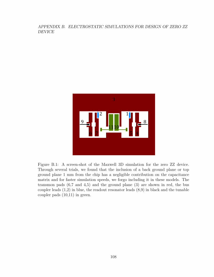
APPENDIX B. ELECTROSTATIC SIMULATIONS FOR DESIGN OF ZERO ZZDEVICE
12
3
456 7
891011
Figure B.1: A screen-shot of the Maxwell 3D simulation for the zero ZZ device.Through several trials, we found that the inclusion of a back ground plane or topground plane 1 mm from the chip has a negligible contribution on the capacitancematrix and for faster simulation speeds, we forgo including it in these models. Thetransmon pads (6,7 and 4,5) and the ground plane (3) are shown in red, the buscoupler leads (1,2) in blue, the readout resonator leads (8,9) in black and the tunablecoupler pads (10,11) in green.
108

Appendix C
Publications and Presentations
• T. M. Hazard1, A. Gyenis1, A. Di Paolo1, A. T. Asfaw, S. A. Lyon, A. Blais,
and A. A. Houck. Nanowire Superinductance Fluxonium Qubit. Phys. Rev.
Lett. 122, 010504 (2019).
• P. S. Mundada1, G. Zhang1, T. M. Hazard1, and A. A. Houck. Suppres-
sion of Qubit Crosstalk in a Tunable Coupling Superconducting Circuit.
arXiv:1810.04182 [quant-ph] (2018).
• T. M. Hazard, A. Gyenis, and A. A. Houck. High Kinetic Inductance Based
Fluxonium Circuit. APS March Meeting, Los Angeles, California, March 2018.
• T. M. Hazard, P. Mundada, G. Zhang, and A. A. Houck. Suppression of static
cross-talk with a tunable coupling element. IARPA LogiQ TEM, Dallas, Texas,
January 2019.
• T. M. Hazard, A. Gyenis, A. Di Paolo, A. T. Asfaw, A. Blais, S. A. Lyon, and A.
A. Houck. Nanowire Superinductance Fluxonium Qubit. APS March Meeting,
Boston, Massachusetts, March 2019.
1Equally contributing author
109
Bibliography
[1] R. P. Feynman. Simulating physics with computers. Int. J. Theor. Phys. 21,467–488 (1982). Cited on page 1.
[2] P. V. Klimov, J. Kelly, Z. Chen, M. Neeley, A. Megrant, B. Burkett,R. Barends, K. Arya, B. Chiaro, Y. Chen, A. Dunsworth, A. Fowler, B. Foxen,C. Gidney, M. Giustina, R. Graff, T. Huang, E. Jeffrey, E. Lucero, J. Y.Mutus, O. Naaman, C. Neill, C. Quintana, P. Roushan, D. Sank,A. Vainsencher, J. Wenner, T. C. White, S. Boixo, R. Babbush, V. N.Smelyanskiy, H. Neven, and J. M. Martinis. Fluctuations of energy-relaxationtimes in superconducting qubits. Phys. Rev. Lett. 121, 090502 (2018). Citedon page 2.
[3] A. Nersisyan, S. Poletto, N. Alidoust, R. Manenti, R. Renzas, C.-V. Bui,K. Vu, T. Whyland, Y. Mohan, E. A. Sete, S. Stanwyck, A. Bestwick, andM. Reagor. Manufacturing low dissipation superconducting quantumprocessors. arXiv:1901.08042, (2019). Cited on page 2.
[4] A. G. Fowler, M. Mariantoni, J. M. Martinis, and A. N. Cleland. Surfacecodes: Towards practical large-scale quantum computation. Phys. Rev. A 86,032324 (2012). Cited on page 2.
[5] T. D. Ladd, F. Jelezko, R. Laflamme, Y. Nakamura, C. Monroe, and J. L.O’Brien. Quantum computers. Nature 464, 45–53 (2010). Cited onpages 2 & 27.
[6] J. M. Gambetta, J. M. Chow, and M. Steffen. Building logical qubits in asuperconducting quantum computing system. npj Quantum Inf. 3, 2 (2017).Cited on page 2.
[7] D. P. DiVincenzo. The physical implementation of quantum computation.Fortschr. Phys. 48, 771–783 (2000). Cited on page 2.
[8] A. Blais, R.-S. Huang, A. Wallraff, S. M. Girvin, and R. J. Schoelkopf. Cavityquantum electrodynamics for superconducting electrical circuits: Anarchitecture for quantum computation. Phys. Rev. A 69, 062320 (2004). Citedon page 3.
110

BIBLIOGRAPHY
[9] R. J. Schoelkopf and S. M. Girvin. Wiring up quantum systems. Nature 451,664–669 (2008). Cited on page 3.
[10] R. Hanson, L. P. Kouwenhoven, J. R. Petta, S. Tarucha, and L. M. K.Vandersypen. Spins in few-electron quantum dots. Rev. Mod. Phys. 79,1217–1265 (2007). Cited on page 3.
[11] C. Kloeffel and D. Loss. Prospects for spin-based quantum computing inquantum dots. Annu. Rev. Condens. Matter Phys. 4, 51–81 (2013). Cited onpage 3.
[12] N. A. Gershenfeld and I. L. Chuang. Bulk spin-resonance quantumcomputation. Science 275, 350–356 (1997). Cited on page 3.
[13] L. M. K. Vandersypen, M. Steffen, G. Breyta, C. S. Yannoni, M. H.Sherwood, and I. L. Chuang. Experimental realization of shor’s quantumfactoring algorithm using nuclear magnetic resonance. Nature 414, 883–887(2001). Cited on page 3.
[14] P. Kok, W. J. Munro, K. Nemoto, T. C. Ralph, J. P. Dowling, and G. J.Milburn. Linear optical quantum computing with photonic qubits. Rev. Mod.Phys. 79, 135–174 (2007). Cited on page 3.
[15] A. Aspuru-Guzik and P. Walther. Photonic quantum simulators. Nat. Phys. 8,285–291 (2012). Cited on page 3.
[16] I. Bloch. Ultracold quantum gases in optical lattices. Nat. Phys. 1, 23–30(2005). Cited on page 3.
[17] I. Bloch, J. Dalibard, and S. Nascimbene. Quantum simulations with ultracoldquantum gases. Nat. Phys. 8, 267–276 (2012). Cited on page 3.
[18] R. Blatt and C. F. Roos. Quantum simulations with trapped ions. Nat. Phys.8, 277–284 (2012). Cited on page 3.
[19] A. Bermudez, X. Xu, R. Nigmatullin, J. O’Gorman, V. Negnevitsky,P. Schindler, T. Monz, U. G. Poschinger, C. Hempel, J. Home,F. Schmidt-Kaler, M. Biercuk, R. Blatt, S. Benjamin, and M. Muller.Assessing the progress of trapped-ion processors towards fault-tolerantquantum computation. Phys. Rev. X 7, 041061 (2017). Cited on page 3.
[20] J. Koch, T. M. Yu, J. Gambetta, A. A. Houck, D. I. Schuster, J. Majer,A. Blais, M. H. Devoret, S. M. Girvin, and R. J. Schoelkopf.Charge-insensitive qubit design derived from the Cooper pair box. Phys. Rev.A 76, 042319 (2007). Cited on pages 3 & 11.
111

BIBLIOGRAPHY
[21] A. A. Houck, J. Koch, M. H. Devoret, S. M. Girvin, and R. J. Schoelkopf. Lifeafter charge noise: Recent results with transmon qubits. Quantum Inf.Process. 8, 105–115 (2009). Cited on page 3.
[22] B. D. Josephson. Possible new effects in superconductive tunnelling. Phys.Lett. 1, 251–253 (1962). Cited on pages 4 & 5.
[23] M. Tinkham. Introduction to Superconductivity. Dover Publications, 2ndedition, 2004. Cited on pages 5, 29, 30 & 50.
[24] V. Ambegaokar and A. Baratoff. Tunneling between superconductors. Phys.Rev. Lett. 10, 486 (1963). Erratum, Phys. Rev. Lett. 11, 104 (1963). Cited onpages 5 & 33.
[25] M. H. Devoret. Quantum fluctuations in electrical circuits. Les HouchesSession LXIII, 351–386 (1995). Cited on page 6.
[26] S. M. Girvin. Circuit QED: Superconducting qubits coupled to microwavephotons. Les Houches Session XCVI, 112–255 (2011). Cited on page 6.
[27] S. Richer. Design of an inductively shunted transmon qubit with tunabletransverse and longitudinal coupling. PhD thesis, RWTH Aachen, 2018. Citedon page 6.
[28] M. A. Nielsen and I. L. Chuang. Quantum Computation and QuantumInformation. Cambridge University Press, 2010. Cited on pages 8, 86, 89,90 & 92.
[29] V. Bouchiat, D. Vion, P. Joyez, D. Esteve, and M. H. Devoret. Quantumcoherence with a single Cooper pair. Phys. Scr. T76, 165–170 (1998). Citedon page 9.
[30] Y. Nakamura, Y. A. Pashkin, and J. S. Tsai. Coherent control of macroscopicquantum states in a single-Cooper-pair box. Nature 398, 786–788 (1999).Cited on page 9.
[31] D. Vion, A. Aassime, A. Cottet, P. Joyez, H. Pothier, C. Urbina, D. Esteve,and M. H. Devoret. Manipulating the quantum state of an electrical circuit.Science 296, 886–889 (2002). Cited on page 9.
[32] J. A. Schreier, A. A. Houck, J. Koch, D. I. Schuster, B. R. Johnson, J. M.Chow, J. M. Gambetta, J. Majer, L. Frunzio, M. H. Devoret, S. M. Girvin,and R. J. Schoelkopf. Suppressing charge noise decoherence in superconductingcharge qubits. Phys. Rev. B 77, 180502(R) (2008). Cited on page 11.
[33] W. D. Oliver and P. B. Welander. Materials in superconducting quantum bits.MRS Bulletin 38, 816–825 (2013). Cited on page 11.
112
BIBLIOGRAPHY
[34] M. H. Devoret and R. J. Schoelkopf. Superconducting circuits for quantuminformation: An outlook. Science 339, 1169–1174 (2013). Cited on page 11.
[35] I. Chiorescu, Y. Nakamura, C. J. P. M. Harmans, and J. E. Mooij. Coherentquantum dynamics of a superconducting flux qubit. Science 299, 1869–1871(2003). Cited on page 12.
[36] J. Koch, V. Manucharyan, M. H. Devoret, and L. I. Glazman. Charging effectsin the inductively shunted josephson junction. Phys. Rev. Lett. 103, 217004(2009). Cited on page 12.
[37] F. Yan, S. Gustavsson, A. Kamal, J. Birenbaum, A. P. Sears, D. Hover, T. J.Gudmundsen, D. Rosenberg, G. Samach, S. Weber, J. L. Yoder, T. P.Orlando, J. Clarke, A. J. Kerman, and W. D. Oliver. The flux qubit revisitedto enhance coherence and reproducibility. Nat. Commun. 7, 12964 (2016).Cited on page 13.
[38] V. E. Manucharyan, J. Koch, L. I. Glazman, and M. H. Devoret. Fluxonium:Single cooper-pair circuit free of charge offsets. Science 326, 113–116 (2009).Cited on pages 14, 29, 53, 56 & 59.
[39] N. A. Masluk, I. M. Pop, A. Kamal, Z. K. Minev, and M. H. Devoret.Microwave characterization of josephson junction arrays: Implementing a lowloss superinductance. Phys. Rev. Lett. 109, 137002 (2012). Cited on pages 14,29, 53 & 69.
[40] U. Vool, I. M. Pop, K. Sliwa, B. Abdo, C. Wang, T. Brecht, Y. Y. Gao,S. Shankar, M. Hatridge, G. Catelani, M. Mirrahimi, L. Frunzio, R. J.Schoelkopf, L. I. Glazman, and M. H. Devoret. Non-poissonian quantumjumps of a fluxonium qubit due to quasiparticle excitations. Phys. Rev. Lett.113, 247001 (2014). Cited on page 14.
[41] D. F. Santavicca, J. K. Adams, L. E. Grant, A. N. McCaughan, and K. K.Berggren. Microwave dynamics of high aspect ratio superconductingnanowires studied using self-resonance. J. Appl. Phys. 119, 234302 (2016).Cited on page 14.
[42] L. Grunhaupt, N. Maleeva, S. T. Skacel, M. Calvo, F. Levy-Bertrand, A. V.Ustinov, H. Rotzinger, A. Monfardini, G. Catelani, and I. M. Pop. Lossmechanisms and quasiparticle dynamics in superconducting microwaveresonators made of thin-film granular aluminum. Phys. Rev. Lett. 121, 117001(2018). Cited on pages 14 & 96.
[43] T. M. Hazard, A. Gyenis, A. Di Paolo, A. T. Asfaw, S. A. Lyon, A. Blais, andA. A. Houck. Nanowire superinductance fluxonium qubit. Phys. Rev. Lett.122, 010504 (2019). Cited on pages 14, 29, 55, 57, 62 & 65.
113

BIBLIOGRAPHY
[44] I. M. Pop, K. Geerlings, G. Catelani, R. J. Schoelkopf, L. I. Glazman, andM. H. Devoret. Coherent suppression of electromagnetic dissipation due tosuperconducting quasiparticles. Nature 508, 369–372 (2014). Cited onpages 15, 17, 28, 59 & 66.
[45] A. A. Houck, J. A. Schreier, B. R. Johnson, J. M. Chow, J. Koch, J. M.Gambetta, D. I. Schuster, L. Frunzio, M. H. Devoret, S. M. Girvin, and R. J.Schoelkopf. Controlling the spontaneous emission of a superconductingtransmon qubit. Phys. Rev. Lett. 101, 080502 (2008). Cited on pages 14,44 & 66.
[46] L. B. Nguyen, Y.-H. Lin, A. Somoroff, R. Mencia, N. Grabon, and V. E.Manucharyan. The high-coherence fluxonium qubit. arXiv:1810.11006,(2018). Cited on pages 16 & 17.
[47] N. Earnest, S. Chakram, Y. Lu, N. Irons, R. K. Naik, N. Leung, L. Ocola,D. A. Czaplewski, B. Baker, J. Lawrence, J. Koch, and D. I. Schuster.Realization of a Λ system with metastable states of a capacitively shuntedfluxonium. Phys. Rev. Lett. 120, 150504 (2018). Cited on pages 16, 17, 53, 56,59 & 67.
[48] Y.-H. Lin, L. B. Nguyen, N. Grabon, J. San Miguel, N. Pankratova, and V. E.Manucharyan. Demonstration of protection of a superconducting qubit fromenergy decay. Phys. Rev. Lett. 120, 150503 (2018). Cited on pages 16, 53, 56,59 & 67.
[49] Z. K. Minev, K. Serniak, I. M. Pop, Z. Leghtas, K. Sliwa, M. Hatridge,L. Frunzio, R. J. Schoelkopf, and M. H. Devoret. Planar multilayer circuitquantum electrodynamics. Phys. Rev. Applied 5, 044021 (2016). Cited onpage 16.
[50] D. Rosenberg, D. Kim, R. Das, D. Yost, S. Gustavsson, D. Hover, P. Krantz,A. Melville, L. Racz, G. O. Samach, S. J. Weber, F. Yan, J. L. Yoder, A. J.Kerman, and W. D. Oliver. 3d integrated superconducting qubits. npjQuantum Information 3, 42 (2017). Cited on page 16.
[51] S. Sheldon, M. Sandberg, H. Paik, B. Abdo, J. M. Chow, M. Steffen, and J. M.Gambetta. Characterization of hidden modes in networks of superconductingqubits. Appl. Phys. Lett. 111, 222601 (2017). Cited on page 16.
[52] V. E. Manucharyan, N. A. Masluk, A. Kamal, J. Koch, L. I. Glazman, andM. H. Devoret. Evidence for coherent quantum phase slips across a josephsonjunction array. Phys. Rev. B 85, 024521 (2012). Cited on pages 17, 29,53 & 70.
114
BIBLIOGRAPHY
[53] A. Kitaev. Protected qubit based on a superconducting current mirror.arXiv:cond-mat/0609441, (2006). Cited on pages 19, 53, 67, 68 & 96.
[54] T. Roy, S. Kundu, M. Chand, S. Hazra, N. Nehra, R. Cosmic, A. Ranadive,M. P. Patankar, K. Damle, and R. Vijay. Implementation of pairwiselongitudinal coupling in a three-qubit superconducting circuit. Phys. Rev.Applied 7, 054025 (2017). Cited on page 19.
[55] S. Richer and D. DiVincenzo. Circuit design implementing longitudinalcoupling: A scalable scheme for superconducting qubits. Phys. Rev. B 93,134501 (2016). Cited on page 19.
[56] P. Brooks, A. Kitaev, and J. Preskill. Protected gates for superconductingqubits. Phys. Rev. A 87, 052306 (2013). Cited on pages 19, 53 & 67.
[57] J. M. Dempster, B. Fu, D. G. Ferguson, D. I. Schuster, and J. Koch.Understanding degenerate ground states of a protected quantum circuit in thepresence of disorder. Phys. Rev. B 90, 094518 (2014). Cited on pages 19,53 & 67.
[58] P. Groszkowski, A. D. Paolo, A. L. Grimsmo, A. Blais, D. I. Schuster, A. A.Houck, and J. Koch. Coherence properties of the 0-π qubit. New Journal ofPhysics 20, 043053 (2018). Cited on pages 22, 23, 53 & 67.
[59] A. Wallraff, D. I. Schuster, A. Blais, L. Frunzio, R.-S. Huang, J. Majer,S. Kumar, S. M. Girvin, and R. J. Schoelkopf. Strong coupling of a singlephoton to a superconducting qubit using circuit quantum electrodynamics.Nature 431, 162–167 (2004). Cited on page 25.
[60] D. I. Schuster, A. A. Houck, J. A. Schreier, A. Wallraff, J. M. Gambetta,A. Blais, L. Frunzio, J. Majer, B. Johnson, M. H. Devoret, S. M. Girvin, andR. J. Schoelkopf. Resolving photon number states in a superconductingcircuit. Nature 445, 515–518 (2007). Cited on pages 25 & 47.
[61] G. Zhu, D. G. Ferguson, V. E. Manucharyan, and J. Koch. Circuit QED withfluxonium qubits: Theory of the dispersive regime. Phys. Rev. B 87, 024510(2013). Cited on page 26.
[62] M. Boissonneault, J. M. Gambetta, and A. Blais. Dispersive regime of circuitQED: Photon-dependent qubit dephasing and relaxation rates. Phys. Rev. A79, 013819 (2009). Cited on page 26.
[63] D. I. Schuster, A. Wallraff, A. Blais, L. Frunzio, R.-S. Huang, J. Majer, S. M.Girvin, and R. J. Schoelkopf. ac Stark shift and dephasing of asuperconducting qubit strongly coupled to a cavity field. Phys. Rev. Lett. 94,123602 (2005). Cited on page 26.
115

BIBLIOGRAPHY
[64] A. A. Clerk, M. H. Devoret, S. M. Girvin, F. Marquardt, and R. J.Schoelkopf. Introduction to quantum noise, measurement, and amplification.Rev. Mod. Phys. 82, 1155–1208 (2010). Cited on page 28.
[65] R. Schoelkopf, A. Clerk, S. Girvin, K. Lehnert, and M. Devoret, Qubits asspectrometers of quantum noise. in Quantum noise in mesoscopic physics,pp. 175–203. Springer, 2003. Cited on pages 28 & 66.
[66] V. E. Manucharyan. Superinductance. PhD thesis, Yale University, 2012.Cited on page 28.
[67] A. J. Annunziata, D. F. Santavicca, L. Frunzio, G. Catelani, M. J. Rooks,A. Frydman, and D. E. Prober. Tunable superconducting nanoinductors.Nanotechnology 21, 445202 (2010). Cited on pages 29 & 30.
[68] J. T. Peltonen, P. C. J. J. Coumou, Z. H. Peng, T. M. Klapwijk, J. S. Tsai,and O. V. Astafiev. Hybrid rf squid qubit based on high kinetic inductance.Scientific Reports 8, 10033 (2018). Cited on page 29.
[69] L. Grunhaupt, M. Spiecker, D. Gusenkova, N. Maleeva, S. T. Skacel,I. Takmakov, F. Valenti, P. Winkel, H. Rotzinger, A. V. Ustinov, et al.Granular aluminum: A superconducting material for high impedance quantumcircuits. arXiv:1809.10646, (2018). Cited on pages 29 & 95.
[70] G. J. Dolan. Offset masks for lift-off photoprocessing. Appl. Phys. Lett. 31,337–339 (1977). Cited on page 33.
[71] F. Lecocq, I. M. Pop, Z. Peng, I. Matei, T. Crozes, T. Fournier, C. Naud,W. Guichard, and O. Buisson. Junction fabrication by shadow evaporationwithout a suspended bridge. Nanotechnology 22, 315302 (2011). Cited onpage 33.
[72] A. Potts, G. J. Parker, J. J. Baumberg, and P. A. J. de Groot. CMOScompatible fabrication methods for submicron Josephson junction qubits. IEEProc. - Sci. Meas. Technol. 148, 225–228 (2001). Cited on page 33.
[73] X. Wu, J. L. Long, H. S. Ku, R. E. Lake, M. Bal, and D. P. Pappas. Overlapjunctions for high coherence superconducting qubits. Appl. Phys. Lett. 111,032602 (2017). Cited on page 33.
[74] A. P. Sears, A. Petrenko, G. Catelani, L. Sun, H. Paik, G. Kirchmair,L. Frunzio, L. I. Glazman, S. M. Girvin, and R. J. Schoelkopf. Photon shotnoise dephasing in the strong-dispersive limit of circuit QED. Phys. Rev. B86, 180504(R) (2012). Cited on page 37.
116

BIBLIOGRAPHY
[75] C. Rigetti, J. M. Gambetta, S. Poletto, B. L. T. Plourde, J. M. Chow, A. D.Corcoles, J. A. Smolin, S. T. Merkel, J. R. Rozen, G. A. Keefe, M. B.Rothwell, M. B. Ketchen, and M. Steffen. Superconducting qubit in awaveguide cavity with a coherence time approaching 0.1 ms. Phys. Rev. B 86,100506(R) (2012). Cited on pages 37 & 79.
[76] J.-H. Yeh, J. LeFebvre, S. Premaratne, F. C. Wellstood, and B. S. Palmer.Microwave attenuators for use with quantum devices below 100 mK. J. Appl.Phys. 121, 224501 (2017). Cited on page 37.
[77] H. T. Friis. A note on a simple transmission formula. Proceedings of the IRE34, 254–256 (1946). Cited on page 38.
[78] D. M. Pozar. Microwave Engineering. Wiley, 4th edition, 2011. Cited onpages 40, 41 & 71.
[79] N. T. Bronn, Y. Liu, J. B. Hertzberg, A. D. Corcoles, A. A. Houck, J. M.Gambetta, and J. M. Chow. Broadband filters for abatement of spontaneousemission in circuit quantum electrodynamics. Appl. Phys. Lett. 107, 172601(2015). Cited on pages 42, 80 & 97.
[80] Y. Liu and A. A. Houck. Quantum electrodynamics near a photonic bandgap.Nat. Phys. 13, 48–52 (2016). Cited on page 42.
[81] N. M. Sundaresan, R. Lundgren, G. Zhu, A. V. Gorshkov, and A. A. Houck.Interacting qubit-photon bound states with superconducting circuits.arXiv:1801.10167 [quant-ph] (2018). Cited on page 42.
[82] R. N. Simons. Coplanar Waveguide Circuits, Components, and Systems. JohnWiley & Sons, 2001. Cited on pages 43 & 71.
[83] K. Geerlings, S. Shankar, E. Edwards, L. Frunzio, R. J. Schoelkopf, and M. H.Devoret. Improving the quality factor of microwave compact resonators byoptimizing their geometrical parameters. Appl. Phys. Lett. 100, 192601(2012). Cited on page 45.
[84] M. S. Khalil, M. J. A. Stoutimore, F. C. Wellstood, and K. D. Osborn. Ananalysis method for asymmetric resonator transmission applied tosuperconducting devices. J. of Appl. Phys. 111, 054510 (2012). Cited onpage 45.
[85] A. Megrant, C. Neill, R. Barends, B. Chiaro, Y. Chen, L. Feigl, J. Kelly,E. Lucero, M. Mariantoni, P. J. J. O’Malley, D. Sank, A. Vainsencher,J. Wenner, T. C. White, Y. Yin, J. Zhao, C. J. Palmstrøm, J. M. Martinis,and A. N. Cleland. Planar superconducting resonators with internal qualityfactors above one million. Appl. Phys. Lett. 100, 113510 (2012). Cited onpage 45.
117
BIBLIOGRAPHY
[86] M. Goppl, A. Fragner, M. Baur, R. Bianchetti, S. Filipp, J. M. Fink, P. J.Leek, G. Puebla, L. Steffen, and A. Wallraff. Coplanar waveguide resonatorsfor circuit quantum electrodynamics. J. Appl. Phys. 104, 113904 (2008).Cited on page 45.
[87] M. D. Reed. Entanglement and Quantum Error Correction withSuperconducting Qubits. PhD thesis, Yale University, 2013. Cited onpages 47 & 85.
[88] A. Wallraff, D. I. Schuster, A. Blais, L. Frunzio, J. Majer, M. H. Devoret,S. M. Girvin, and R. J. Schoelkopf. Approaching unit visibility for control of asuperconducting qubit with dispersive readout. Phys. Rev. Lett. 95, 060501(2005). Cited on page 48.
[89] D. I. Schuster. Circuit Quantum Electrodynamics. PhD thesis, Yale University,2007. Cited on page 49.
[90] N. Maleeva, L. Grunhaupt, T. Klein, F. Levy-Bertrand, O. Dupre, M. Calvo,F. Valenti, P. Winkel, F. Friedrich, W. Wernsdorfer, A. V. Ustinov,H. Rotzinger, A. Monfardini, M. V. Fistul, and I. M. Pop. Circuit quantumelectrodynamics of granular aluminum resonators. Nature Communications 9,3889 (2018). Cited on pages 51 & 95.
[91] G. Calusine, A. Melville, W. Woods, R. Das, C. Stull, V. Bolkhovsky,D. Braje, D. Hover, D. K. Kim, X. Miloshi, D. Rosenberg, A. Sevi, J. L.Yoder, E. Dauler, and W. D. Oliver. Analysis and mitigation of interfacelosses in trenched superconducting coplanar waveguide resonators. Appl. Phys.Lett. 112, 062601 (2018). Cited on page 51.
[92] W. Woods, G. Calusine, A. Melville, A. Sevi, E. Golden, D. K. Kim,D. Rosenberg, J. L. Yoder, and W. D. Oliver. Determining interface dielectriclosses in superconducting coplanar waveguide resonators. arXiv:1808.10347,(2018). Cited on page 51.
[93] M. T. Bell, I. A. Sadovskyy, L. B. Ioffe, A. Y. Kitaev, and M. E. Gershenson.Quantum superinductor with tunable nonlinearity. Phys. Rev. Lett. 109,137003 (2012). Cited on page 53.
[94] L. B. Ioffe, M. V. Feigel’man, A. Ioselevich, D. Ivanov, M. Troyer, andG. Blatter. Topologically protected quantum bits using josephson junctionarrays. Nature 415, 503–506 (2002). Cited on page 53.
[95] A. Wallraff, D. I. Schuster, A. Blais, J. M. Gambetta, J. Schreier, L. Frunzio,M. H. Devoret, S. M. Girvin, and R. J. Schoelkopf. Sideband transitions andtwo-tone spectroscopy of a superconducting qubit strongly coupled to anon-chip cavity. Phys. Rev. Lett. 99, 050501 (2007). Cited on page 57.
118

BIBLIOGRAPHY
[96] J. Bourassa, F. Beaudoin, J. M. Gambetta, and A. Blais.Josephson-junction-embedded transmission-line resonators: From kerr mediumto in-line transmon. Phys. Rev. A 86, 013814 (2012). Cited on page 58.
[97] H. L. Mortensen, K. Mølmer, and C. K. Andersen. Normal modes of asuperconducting transmission-line resonator with embedded lumped elementcircuit components. Phys. Rev. A 94, 053817 (2016). Cited on page 58.
[98] A. Kou, W. C. Smith, U. Vool, R. T. Brierley, H. Meier, L. Frunzio, S. M.Girvin, L. I. Glazman, and M. H. Devoret. Fluxonium-based artificialmolecule with a tunable magnetic moment. Phys. Rev. X 7, 031037 (2017).Cited on pages 59, 70 & 95.
[99] M. Baur, S. Filipp, R. Bianchetti, J. M. Fink, M. Goppl, L. Steffen, P. J.Leek, A. Blais, and A. Wallraff. Measurement of autler-townes and mollowtransitions in a strongly driven superconducting qubit. Phys. Rev. Lett. 102,243602 (2009). Cited on page 60.
[100] M. A. Sillanpaa, J. Li, K. Cicak, F. Altomare, J. I. Park, R. W. Simmonds,G. S. Paraoanu, and P. J. Hakonen. Autler-townes effect in a superconductingthree-level system. Phys. Rev. Lett. 103, 193601 (2009). Cited on page 60.
[101] S. Novikov, J. E. Robinson, Z. K. Keane, B. Suri, F. C. Wellstood, and B. S.Palmer. Autler-townes splitting in a three-dimensional transmonsuperconducting qubit. Phys. Rev. B 88, 060503 (2013). Cited on page 60.
[102] B. Suri, Z. K. Keane, R. Ruskov, L. S. Bishop, C. Tahan, S. Novikov, J. E.Robinson, F. C. Wellstood, and B. S. Palmer. Observation of autler–towneseffect in a dispersively dressed jaynes–cummings system. New Journal ofPhysics 15, 125007 (2013). Cited on page 60.
[103] M. J. Peterer, S. J. Bader, X. Jin, F. Yan, A. Kamal, T. J. Gudmundsen, P. J.Leek, T. P. Orlando, W. D. Oliver, and S. Gustavsson. Coherence and decayof higher energy levels of a superconducting transmon qubit. Phys. Rev. Lett.114, 010501 (2015). Cited on page 63.
[104] H. Paik, D. I. Schuster, L. S. Bishop, G. Kirchmair, G. Catelani, A. P. Sears,B. R. Johnson, M. J. Reagor, L. Frunzio, L. I. Glazman, S. M. Girvin, M. H.Devoret, and R. J. Schoelkopf. Observation of high coherence in Josephsonjunction qubits measured in a three-dimensional circuit QED architecture.Phys. Rev. Lett. 107, 240501 (2011). Cited on page 66.
[105] A. D. Paolo, A. Grimsmo, P. Groszkowski, J. Koch, and A. Blais. Control andcoherence time enhancement of the 0-pi qubit. New Journal of Physics,(2019). Cited on pages 68 & 97.
119

BIBLIOGRAPHY
[106] U. Vool, A. Kou, W. C. Smith, N. E. Frattini, K. Serniak, P. Reinhold, I. M.Pop, S. Shankar, L. Frunzio, S. M. Girvin, and M. H. Devoret. Drivingforbidden transitions in the fluxonium artificial atom. Phys. Rev. Applied 9,054046 (2018). Cited on page 68.
[107] D. E. Anagnostou, M. Morton, J. Papapolymerou, and C. G. Christodoulou. A0–55-ghz coplanar waveguide to coplanar strip transition. IEEE Transactionson Microwave Theory and Techniques 56, 1–6 (2008). Cited on page 72.
[108] L. DiCarlo, M. D. Reed, L. Sun, B. R. Johnson, J. M. Chow, J. M. Gambetta,L. Frunzio, S. M. Girvin, M. H. Devoret, and R. J. Schoelkopf. Preparationand measurement of three-qubit entanglement in a superconducting circuit.Nature 467, 574 (2010). Cited on page 76.
[109] C. Rigetti and M. Devoret. Fully microwave-tunable universal gates insuperconducting qubits with linear couplings and fixed transition frequencies.Phys. Rev. B 81, 134507 (2010). Cited on page 76.
[110] J. M. Gambetta, A. D. Corcoles, S. T. Merkel, B. R. Johnson, J. A. Smolin,J. M. Chow, C. A. Ryan, C. Rigetti, S. Poletto, T. A. Ohki, M. B. Ketchen,and M. Steffen. Characterization of addressability by simultaneous randomizedbenchmarking. Phys. Rev. Lett. 109, 240504 (2012). Cited on page 77.
[111] J. M. Chow, A. D. Corcoles, J. M. Gambetta, C. Rigetti, B. R. Johnson, J. A.Smolin, J. R. Rozen, G. A. Keefe, M. B. Rothwell, M. B. Ketchen, andM. Steffen. Simple all-microwave entangling gate for fixed-frequencysuperconducting qubits. Phys. Rev. Lett. 107, 080502 (2011). Cited onpage 77.
[112] M. Takita, A. D. Corcoles, E. Magesan, B. Abdo, M. Brink, A. Cross, J. M.Chow, and J. M. Gambetta. Demonstration of weight-four paritymeasurements in the surface code architecture. Phys. Rev. Lett. 117, 210505(2016). Cited on pages 77 & 97.
[113] M. Takita, A. W. Cross, A. D. Corcoles, J. M. Chow, and J. M. Gambetta.Experimental demonstration of fault-tolerant state preparation withsuperconducting qubits. Phys. Rev. Lett. 119, 180501 (2017). Cited onpage 77.
[114] L. DiCarlo, J. M. Chow, J. M. Gambetta, L. S. Bishop, B. R. Johnson, D. I.Schuster, J. Majer, A. Blais, L. Frunzio, S. M. Girvin, and R. J. Schoelkopf.Demonstration of two-qubit algorithms with a superconducting quantumprocessor. Nature 460, 240–244 (2009). Cited on page 77.
120

BIBLIOGRAPHY
[115] G. Zhang. Tunable Coupling and Its Applications in Circuit QuantumElectrodynamics. PhD thesis, Princeton University, 2018. Cited on pages 77,78, 79, 82 & 87.
[116] M. D. Reed, B. R. Johnson, A. A. Houck, L. DiCarlo, J. M. Chow, D. I.Schuster, L. Frunzio, and R. J. Schoelkopf. Fast reset and suppressingspontaneous emission of a superconducting qubit. Appl. Phys. Lett. 96,203110 (2010). Cited on pages 80 & 97.
[117] M. D. Hutchings, J. B. Hertzberg, Y. Liu, N. T. Bronn, G. A. Keefe,M. Brink, J. M. Chow, and B. L. T. Plourde. Tunable superconducting qubitswith flux-independent coherence. Phys. Rev. Applied 8, 044003 (2017). Citedon page 81.
[118] B. M. Vlastakis. Controlling coherent state superpositions withsuperconducting circuits. PhD thesis, Yale University, 2015. Cited on page 84.
[119] J. M. Chow, L. DiCarlo, J. M. Gambetta, F. Motzoi, L. Frunzio, S. M. Girvin,and R. J. Schoelkopf. Optimized driving of superconducting artificial atomsfor improved single-qubit gates. Phys. Rev. A 82, 040305(R) (2010). Cited onpage 85.
[120] E. Knill, D. Leibfried, R. Reichle, J. Britton, R. B. Blakestad, J. D. Jost,C. Langer, R. Ozeri, S. Seidelin, and D. J. Wineland. Randomizedbenchmarking of quantum gates. Phys. Rev. A 77, 012307 (2008). Cited onpage 86.
[121] J. M. Chow, J. M. Gambetta, L. Tornberg, J. Koch, L. S. Bishop, A. A.Houck, B. R. Johnson, L. Frunzio, S. M. Girvin, and R. J. Schoelkopf.Randomized benchmarking and process tomography for gate errors in asolid-state qubit. Phys. Rev. Lett. 102, 090502 (2009). Cited on page 86.
[122] A. D. Corcoles, J. M. Gambetta, J. M. Chow, J. A. Smolin, M. Ware,J. Strand, B. L. T. Plourde, and M. Steffen. Process verification of two-qubitquantum gates by randomized benchmarking. Phys. Rev. A 87, 030301(R)(2013). Cited on pages 86 & 87.
[123] J. P. Gaebler, A. M. Meier, T. R. Tan, R. Bowler, Y. Lin, D. Hanneke, J. D.Jost, J. P. Home, E. Knill, D. Leibfried, and D. J. Wineland. Randomizedbenchmarking of multiqubit gates. Phys. Rev. Lett. 108, 260503 (2012). Citedon page 87.
[124] E. Magesan, J. M. Gambetta, and J. Emerson. Scalable and robustrandomized benchmarking of quantum processes. Phys. Rev. Lett. 106, 180504(2011). Cited on page 87.
121

BIBLIOGRAPHY
[125] P. Bertet, C. J. P. M. Harmans, and J. E. Mooij. Parametric coupling forsuperconducting qubits. Phys. Rev. B 73, 064512 (2006). Cited on page 87.
[126] A. O. Niskanen, K. Harrabi, F. Yoshihara, Y. Nakamura, S. Lloyd, and J. S.Tsai. Quantum coherent tunable coupling of superconducting qubits. Science316, 723–726 (2007). Cited on page 87.
[127] E. Kapit. Universal two-qubit interactions, measurement, and cooling forquantum simulation and computing. Phys. Rev. A 92, 012302 (2015). Citedon page 87.
[128] J. Majer, J. M. Chow, J. M. Gambetta, J. Koch, B. R. Johnson, J. A.Schreier, L. Frunzio, D. I. Schuster, A. A. Houck, A. Wallraff, A. Blais, M. H.Devoret, S. M. Girvin, and R. J. Schoelkopf. Coupling superconducting qubitsvia a cavity bus. Nature 449, 443–447 (2007). Cited on page 87.
[129] A. Dewes, F. R. Ong, V. Schmitt, R. Lauro, N. Boulant, P. Bertet, D. Vion,and D. Esteve. Characterization of a two-transmon processor with individualsingle-shot qubit readout. Phys. Rev. Lett. 108, 057002 (2012). Cited onpages 87 & 90.
[130] R. C. Bialczak, M. Ansmann, M. Hofheinz, E. Lucero, M. Neeley, A. D.O’Connell, D. Sank, H. Wang, J. Wenner, M. Steffen, A. N. Cleland, andJ. M. Martinis. Quantum process tomography of a universal entangling gateimplemented with josephson phase qubits. Nature Physics 6, 409 (2010).Cited on page 88.
[131] D. C. McKay, S. Filipp, A. Mezzacapo, E. Magesan, J. M. Chow, and J. M.Gambetta. Universal gate for fixed-frequency qubits via a tunable bus. Phys.Rev. Appl. 6, 064007 (2016). Cited on page 89.
[132] J. M. Chow. Quantum Information Processing with Superconducting Qubits.PhD thesis, Yale University, 2010. Cited on page 92.
[133] E. Magesan and J. M. Gambetta. Effective hamiltonian models of thecross-resonance gate. arXiv:1804.04073, (2018). Cited on pages 92 & 94.
[134] S. Sheldon, E. Magesan, J. M. Chow, and J. M. Gambetta. Procedure forsystematically tuning up cross-talk in the cross-resonance gate. Phys. Rev. A93, 060302(R) (2016). Cited on page 94.
122