ieee transactions on microwave theory and...
TRANSCRIPT

IEEE TRANSACTIONS ON MICROWAVE THEORY AND TECHNIQUES, VOL. 64, NO. 7, JULY 2016 2113
Variable 360° Vector-Sum Phase ShifterWith Coarse and Fine Vector Scaling
Mohammad-Mahdi Mohsenpour, Member, IEEE, and Carlos E. Saavedra, Senior Member, IEEE
Abstract— A CMOS vector-sum phase shifter covering the full360° range is presented in this paper. Broadband operationaltransconductance amplifiers with variable transconductance pro-vide coarse scaling of the quadrature vector amplitudes. Finescaling of the amplitudes is accomplished using a passive resistivenetwork. Expressions are derived to predict the maximum bitresolution of the phase shifter from the scaling factor of the coarseand fine vector-scaling stages. The phase shifter was designedand fabricated using the standard 130-nm CMOS process andwas tested on-wafer over the frequency range of 4.9–5.9 GHz.The phase shifter delivers root mean square (rms) phase andamplitude errors of 1.25° and 0.7 dB, respectively, at the midbandfrequency of 5.4 GHz. The input and output return losses areboth below 17 dB over the band, and the insertion loss is betterthan 4 dB over the band. The circuit uses an area of 0.303 mm2
excluding bonding pads and draws 28 mW from a 1.2 V supply.
Index Terms— Active phase shifter, active summing junction,clock and data recovery, CMOS, IEEE 802.11n, LTE, monolithicmicrowave integrated circuit (MMIC), operational transconduc-tance amplifiers (OTAs), phased array, quadrature generation,radar, RFIC, root mean square (rms) error, WiMAX.
I. INTRODUCTION
THERE is continued interest in finding new methodsto improve the resolution and accuracy of monolithic
microwave integrated circuit (MMIC) phase shifters. Thatinterest is motivated by the critical role that phase shifters havein multiple-input multiple output radio links and phased arrays.Design advances over the past decade have led to significantimprovements in the fractional bandwidth of the phase shiftersand a reduction in the footprint area of the chips. MMICphase shifters covering the full 360° using different tech-niques, such as delay lines [1], [2], signal reflection [3], high-pass/low-pass networks [4], all-pass networks [5], and vectorsummation [6]–[12].
In vector-sum phase shifters, there often appear unreachablephase angles (phase gaps) at the quadrant edges that limitthe phase-step (bit) resolution of digital phase shifters. Theobjective of this paper is to explore the issue of phase gapsin vector-sum phase shifters and to propose a solution tomitigate them. The general approach taken here is to use a two-step vector-scaling procedure. First, a coarse scaling is carried
Manuscript received April 6, 2015; revised August 18, 2015,February 9, 2016, and April 25, 2016; accepted May 21, 2016. Dateof publication June 14, 2016; date of current version July 7, 2016. This workwas supported by the Natural Science and Engineering Research Council ofCanada.
The authors are with the Department of Electrical and Computer Engi-neering, Queen’s University, Kingston, ON K7L 3N6, Canada (e-mail:[email protected]; [email protected]).
Color versions of one or more of the figures in this paper are availableonline at http://ieeexplore.ieee.org.
Digital Object Identifier 10.1109/TMTT.2016.2574843
out in the current domain using operational transconductanceamplifiers (OTAs), and subsequently, fine scaling is done onthe signal vector in the voltage domain using a resistive net-work before the signal vectors are added together. A prototypephase shifter was designed for the 5.4-GHz band and wasfabricated using the 130-nm CMOS technology. Experimentaltest results are presented, which validate the concept.
II. PHASE SHIFTER CONCEPT
Fig. 1 shows the block diagram of the proposed MMICphase shifter, where the shaded area shows the on-chip cir-cuitry. The phasor diagrams above the shaded area illustratehow a representative input signal is modified as it propagatesthrough the phase shifter. The external 180° power splitterconverts the RF input voltage signal, vRF, into a differentialwaveform. A quadrature generator then produces four equal-amplitude orthogonal voltage signal vectors, ±v I and ±vQ , forthe I and Q paths, respectively. A pair of identical OTAs areused to scale the magnitude of the four voltage signal vectorsand to convert them into current signals: ±i I,Q = ±Gmv I,Q ,where Gm is the transconductance gain of the OTAs, which istuned through the analog control voltages Vtune,I and Vtune,Q .
Two single-pole double-throw (SPDT) switches are used toselect which I -path vector (the 0° or the 180°) and whichQ-path vector (the 90° or the 270°) will be summed togetherat the output to produce the desired output phase angle. TheSPDT switches are controlled using two digital bits, a2b2.
While the minimum gain, Gmin, of the OTAs can ostensiblybe reduced to zero, the problem with doing so is that the phaseresponse of the OTAs at zero gain can be quite different thanat moderate to high gain levels, thereby compromising the rootmean square (rms) phase and amplitude error performance ofthe circuit. As a result, there is a practical limit to how smallGmin should be and that value can be found by observing thephase response of the OTA as a function of its gain.
Suppose now that Gmin has been established and that thehighest gain setting of the OTAs is denoted by Gmax, then thesmallest output angle that the phase shifter would produce inquadrant I is
θmin = tan−1(
Gmin,Q
Gmax,I
)rad (1)
as shown in Fig. 2(a). It is straightforward to see that therewill be a range of phase angles that the phase shifter cannotproduce between quadrants I and IV and at every otherquadrant boundary, as shown in Fig. 2(b). These unreachableoutput phase angle regions are the so-called phase gaps. Thesize of the gaps is θgap = 2θmin and they place a limit on the bit
0018-9480 © 2016 IEEE. Personal use is permitted, but republication/redistribution requires IEEE permission.See http://www.ieee.org/publications_standards/publications/rights/index.html for more information.

2114 IEEE TRANSACTIONS ON MICROWAVE THEORY AND TECHNIQUES, VOL. 64, NO. 7, JULY 2016
Fig. 1. Block diagram of the 360° vector-sum phase shifter proposed in this paper. Components outside the shaded area are off-chip.
Fig. 2. (a) Minimum output phase angle, θmin, that can be produced inquadrant I. (b) Phase gaps equal to 2θmin occur at the quadrant boundaries.
resolution of digital vector-sum phase shifters, since the circuitcannot have a phase step smaller than θgap. The relationshipbetween the phase gap and the phase-step resolution of thephase shifter is θgap < 2π/2n , from which the maximumbit resolution is �n� = log2(2π/θgap), where �·� denotes the
floor function. With the aid of (1), the expression for themaximum bit resolution, n, of the phase shifter as a functionof the amplifier gain tuning range is
�n� = log2
⎡⎣ π
tan−1(
Gmin,QGmax,I
)⎤⎦ . (2)
To reduce the size of θgap and thereby increase the bit resolu-tion of the phase shifter, the proposed system in Fig. 1 employsthe second vector-scaling step after the SPDT switches. Thissecond scaling step is done with a resistive passive network.The final I and Q vectors are added using a summing junctionto produce the desired phase-shifted signal.
III. RFIC DESIGN
This section provides design details of the phase shifter’sbuilding blocks in sequence from left to right. All cir-cuit components were designed for a center frequencyof 5.4 GHz.

MOHSENPOUR AND SAAVEDRA: VARIABLE 360◦ VECTOR-SUM PHASE SHIFTER 2115
Fig. 3. Schematic of the all-pass quadrature signal generator.
A. Quadrature Signal Generator
The circuit shown in Fig. 3 is used to generate differentialquadrature basis vectors for the I and Q signal paths. It isan all-pass network that yields signals with tight amplitudeand phase balance over wide bandwidths with a low returnloss at the input port [6]. Using the component values shownin Fig. 3, the simulation results predict phase and amplitudeimbalances less than 1° and 0.35 dB, respectively, and an inputreturn loss below 16 dB for the quadrature generator over a1-GHz band centered at 5.4 GHz.
B. OTA Vector-Scaling Stage (Coarse Scaling)
The OTAs convert the incident voltage signals into cur-rents. These signal currents are then scaled by varying thetransconductance, Gm , of the OTAs. The OTA schematic isshown in Fig. 4 and is a variant of the circuit reportedin [7] and [13]–[15]. Thus, only a basic description of the OTAis given here followed by the information relevant to the phaseshifter design. The input signal feeds to M1/M2 and M5/M6through C1/C2 and C5/C6, respectively. Transistors M3 and M4are cross-coupled to provide feedforward regulation to theOTA for broadband operation and increased linearity. Tuningof the Gm is done by changing the gate voltage of M3/M4at the node labeled Vtune in Fig. 4. Triple well nMOSdevices are used here to provide source-body isolation for allOTA’s devices and better isolation from substrate. CapacitorsC3 and C4 are for dc blocking, and resistors R1–R6 have alarge value and are used for dc biasing.
A key design goal for the OTA for the application athand is for its gain, Gm , versus Vtune relationship to havea linear response, so that the vector scaling also exhibits alinear dependence on the tuning voltage. A simulation of Gm
versus control voltage, Vtune, at a frequency of 5.4 GHz isshown in Fig. 5. The magnitude of Gm varies linearly from5.5 to 32 mS as Vtune is swept from 0.45 to 0.85 V. Therefore,θgap = 2tan−1(5.5/32) = 0.34 rad = 19.5° and (2) predictsthat the highest resolution that the phase shifter could produceis 4 b which corresponds to a phase step of 22.5°. To improve
Fig. 4. Schematic of the tunable feedforward-regulated OTA for coarse vectorscaling.
Fig. 5. Simulation results for amplitude and phase variations of the OTAversus control voltage.
the resolution of the phase shifter, the second scaling circuitis used to reduce the value of Gm . That circuit is describedfurther below after the SPDT switches.
C. SPDT Switches
Two SPDT switches, connected to the OTAs’ outputs,choose between the four quadrants. To keep the insertionloss of the switches below 1 dB, two series nMOS transistor,M7 and M8, are used to provide a low channel resistance.
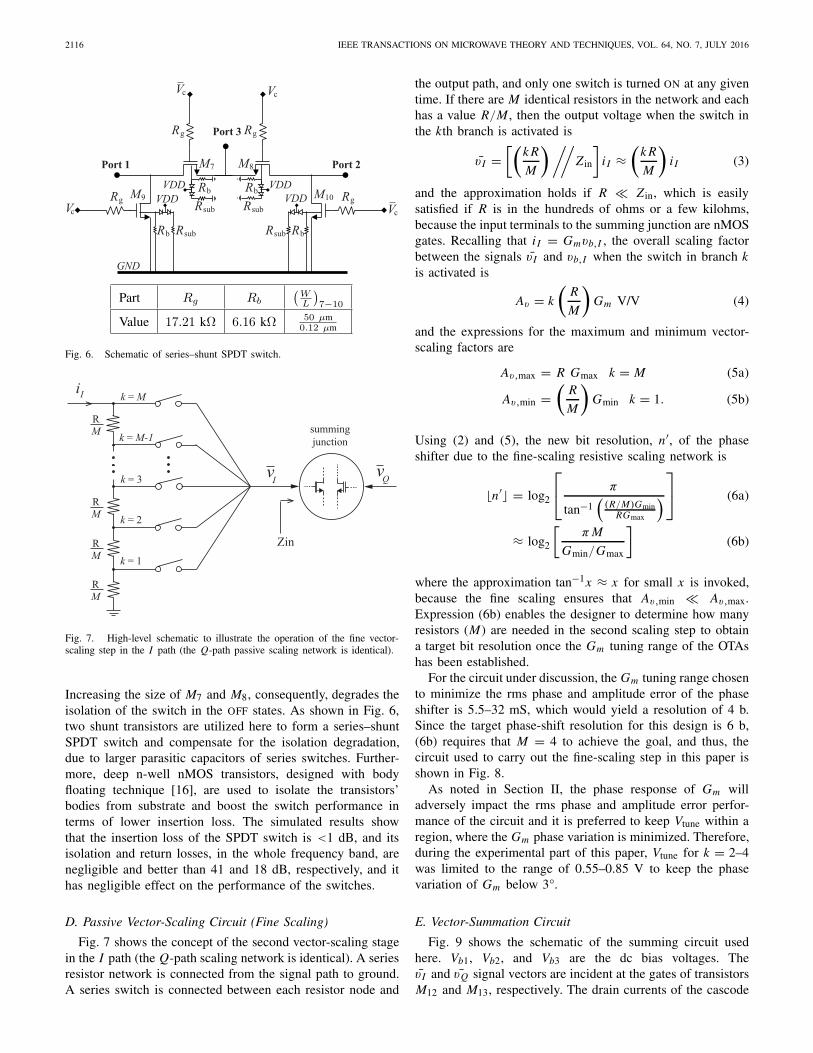
2116 IEEE TRANSACTIONS ON MICROWAVE THEORY AND TECHNIQUES, VOL. 64, NO. 7, JULY 2016
Fig. 6. Schematic of series–shunt SPDT switch.
Fig. 7. High-level schematic to illustrate the operation of the fine vector-scaling step in the I path (the Q-path passive scaling network is identical).
Increasing the size of M7 and M8, consequently, degrades theisolation of the switch in the OFF states. As shown in Fig. 6,two shunt transistors are utilized here to form a series–shuntSPDT switch and compensate for the isolation degradation,due to larger parasitic capacitors of series switches. Further-more, deep n-well nMOS transistors, designed with bodyfloating technique [16], are used to isolate the transistors’bodies from substrate and boost the switch performance interms of lower insertion loss. The simulated results showthat the insertion loss of the SPDT switch is <1 dB, and itsisolation and return losses, in the whole frequency band, arenegligible and better than 41 and 18 dB, respectively, and ithas negligible effect on the performance of the switches.
D. Passive Vector-Scaling Circuit (Fine Scaling)
Fig. 7 shows the concept of the second vector-scaling stagein the I path (the Q-path scaling network is identical). A seriesresistor network is connected from the signal path to ground.A series switch is connected between each resistor node and
the output path, and only one switch is turned ON at any giventime. If there are M identical resistors in the network and eachhas a value R/M , then the output voltage when the switch inthe kth branch is activated is
v̄ I =[(
k R
M
) //Z in
]i I ≈
(k R
M
)i I (3)
and the approximation holds if R � Z in, which is easilysatisfied if R is in the hundreds of ohms or a few kilohms,because the input terminals to the summing junction are nMOSgates. Recalling that i I = Gmvb,I , the overall scaling factorbetween the signals v̄ I and vb,I when the switch in branch kis activated is
Av = k
(R
M
)Gm V/V (4)
and the expressions for the maximum and minimum vector-scaling factors are
Av,max = R Gmax k = M (5a)
Av,min =(
R
M
)Gmin k = 1. (5b)
Using (2) and (5), the new bit resolution, n′, of the phaseshifter due to the fine-scaling resistive scaling network is
�n′� = log2
⎡⎣ π
tan−1(
(R/M)GminRGmax
)⎤⎦ (6a)
≈ log2
[π M
Gmin/Gmax
](6b)
where the approximation tan−1x ≈ x for small x is invoked,because the fine scaling ensures that Av,min � Av,max.Expression (6b) enables the designer to determine how manyresistors (M) are needed in the second scaling step to obtaina target bit resolution once the Gm tuning range of the OTAshas been established.
For the circuit under discussion, the Gm tuning range chosento minimize the rms phase and amplitude error of the phaseshifter is 5.5–32 mS, which would yield a resolution of 4 b.Since the target phase-shift resolution for this design is 6 b,(6b) requires that M = 4 to achieve the goal, and thus, thecircuit used to carry out the fine-scaling step in this paper isshown in Fig. 8.
As noted in Section II, the phase response of Gm willadversely impact the rms phase and amplitude error perfor-mance of the circuit and it is preferred to keep Vtune within aregion, where the Gm phase variation is minimized. Therefore,during the experimental part of this paper, Vtune for k = 2–4was limited to the range of 0.55–0.85 V to keep the phasevariation of Gm below 3°.
E. Vector-Summation Circuit
Fig. 9 shows the schematic of the summing circuit usedhere. Vb1, Vb2, and Vb3 are the dc bias voltages. Thev̄ I and ¯vQ signal vectors are incident at the gates of transistorsM12 and M13, respectively. The drain currents of the cascode

MOHSENPOUR AND SAAVEDRA: VARIABLE 360◦ VECTOR-SUM PHASE SHIFTER 2117
Fig. 8. Schematic of the four-resistor network used for fine vector scaling.
Fig. 9. Schematic of the vector-summation circuit.
transistors M14 and M15 are added at node A and are fed to atransimpedance amplifier. A source-follower (M21) is used asa buffer to isolate the phase shifter from the 50-� impedanceenvironment of the measurement system.
IV. EXPERIMENTAL RESULTS
The OTA-based active phase shifter is fabricated using theGlobal Foundries (formerly IBM) 0.13-μm CMOS process.A microphotograph of the fabricated chip is shown in Fig. 10.The chip core occupies an area of 0.303 mm2 excludingbonding pads. The circuit draws a maximum of 28 mW ofdc power from a 1.2 V supply.
An Agilent 8510C vector network analyzer was used formeasuring the insertion phase and gain of the chip in different
Fig. 10. Microphotograph of the fabricated active phase shifter.
Fig. 11. Measurement and simulation results for input and output returnlosses.
phase settings. The chip’s differential input signals are fed byan external hybrid coupler, Krytar 4010180 with around 0.5 dBloss in 5-GHz band.
As noted earlier, the input and output matching circuitries ofthe phase shifter are independent of the phase shifter’s phasesetting. Therefore, the input and output reflection coefficients,S11 and S22, are provided for just one phase setting. Fig. 11shows the input and output return losses. The measurementand simulation results agree for both S11 and S22. Thereturn losses are better than 15 dB in the frequency bandof interest. Required tuning voltages for I and Q paths,Vtune,I and Vtune,Q , are varied with 10-mV quantization steps,and their values and digital controls (refine bits) are providedin a lookup table.
Fig. 12 shows the unwrapped measured insertion phaseresponse for 64 different phase states spaced 5.625° apart(6-b resolution). Both the measured and ideal relative insertion

2118 IEEE TRANSACTIONS ON MICROWAVE THEORY AND TECHNIQUES, VOL. 64, NO. 7, JULY 2016
Fig. 12. Measured insertion phase for 64 output phases.
Fig. 13. Measured (solid lines) and ideal (dashed lines) relative insertionphase for 16 out of 64 possible states.
phases of the circuit are shown in Fig. 13. Only 16 out ofthe 64 possible curves are shown to avoid an overcrowdedplot. As expected, the best agreement between the measuredand ideal curves in Fig. 13 occurs at the design frequencyof 5.4 GHz.
The rms phase error of a phase shifter can be calculatedusing (7), where N is equal to number of phase states(64 in this paper) and θ�i is the difference between thephase angle produced by the phase shifter and the expectedtheoretical value. The rms phase error of the proposed phaseshifter is 1.25° at 5.4 GHz. The rms phase error as a functionof frequency is shown in Fig. 14. The simulated and measuredgroup delays are 0.11 and 0.14 ns, respectively,
θ�,RMS =√√√√ 1
N − 1×
N∑i=2
|θ�i |2 (°) (7)
A�,RMS =√√√√ 1
N×
N∑i=1
|A�i |2 (dB). (8)
Fig. 15 shows the insertion gain responses for some of thephase states (16 states are chosen for better illustration). Therms gain error, calculated using (8) for all 64 settings, is always
Fig. 14. RMS phase error.
Fig. 15. Measured insertion gain for 16 states out of 64 phase settings (formore clear demonstration).
Fig. 16. RMS amplitude error.
less than 0.7 dB, as shown in Fig. 16. The degradation ofthe measurement results from the simulations is <0.5 dB andexperiences its maximum as it reaches the frequency band’sedges. Here, A�i is the deviation of the gain response in each
MOHSENPOUR AND SAAVEDRA: VARIABLE 360◦ VECTOR-SUM PHASE SHIFTER 2119
TABLE I
PERFORMANCE SUMMARY AND COMPARISON TABLE
Fig. 17. Distribution of (a) phase and (b) magnitude deviation with mismatchin Monte Carlo simulation with 1000 runs.
phase state from the average insertion gain in decibel scales.The measured maximum peak to peak insertion gain error is−1.24 to 1.06 dB at 5.4 GHz, while its average value is −1 dB.
A Monte Carlo simulation was carried out to examinethe effect of device mismatches on the amplitude and phasevariations of the phase shifter. Fig. 17 shows the Monte Carloresults for a representative phase state of 0°. The stan-dard deviation of the phase angle for eight phase states
Fig. 18. Measured constellation diagram of the phase shifter.
around 360° is always less than 1.7°, which is well belowthe resolution of the phase shifter (5.625°). Meanwhile, thestandard deviation of the amplitude variation is below 0.15 dB.The 72.5% of the occurrences (out of 1000 runs) were less than0.25 of the least significant phase shift (±1.2°) away from themean value of that state. The polar plot, shown in Fig. 18,shows the uniform distribution for all 64 constellation statesof the phase shifter, normalized to the average insertion gain.
Fig. 19 shows the measured output power versus inputpower to study the linearity performance of the phase shifterat 5.4 GHz. The input-referred 1-dB compression point is−12.9 dB. The simulation results show that the 1-dB compres-sion point variation, for all the phase states, is less than ±1 dB.This is in accordance with the 2-dB insertion gain variationin different phase settings, reported by the measurements. Thesimulation result for the noise figure is also around 20 dB forall phase states.
A summary of the phase shifter’s performance is outlinedin Table I, in conjunction with a comparison with some of thepreviously reported designs in the similar CMOS technology.

2120 IEEE TRANSACTIONS ON MICROWAVE THEORY AND TECHNIQUES, VOL. 64, NO. 7, JULY 2016
Fig. 19. Measured P1-dB compression point for the 0° phase setting.
Table I also includes the calculation of a basic metric
A�,RMS × θ�,RMS (9)
for each circuit consisting of the product of the rms amplitudeand phase errors. The metric is calculated at the centerfrequency and has the units of [dB][°].
V. CONCLUSION
A high-accuracy low rms error phase shifter based on thevector-sum method is demonstrated in this paper. The useof coarse and fine scaling of the signal vectors is criticalto reducing phase gaps between quadrants and for reducingtherms phase and amplitude errors. Experimental tests on afabricated prototype showed that therms phase error reacheddown to 1.25°, and therms amplitude error was 0.7 dB at thecenter frequency of 5.4 GHz, thereby validating the approach.
ACKNOWLEDGMENT
The authors would like to thank CMC Microsystems,Kingston, ON, Canada, for chip fabrication arrangements.
REFERENCES
[1] F. Ellinger, H. Jackel, and W. Bachtold, “Varactor-loaded transmission-line phase shifter at C-band using lumped elements,” IEEE Trans.Microw. Theory Techn., vol. 51, no. 4, pp. 1135–1140, Apr. 2003.
[2] R. Amirkhanzadeh, H. Sjöland, J.-M. Redouté, D. Nobbe, andM. Faulkner, “High-resolution passive phase shifters for adaptive duplex-ing applications in sos process,” IEEE Trans. Microw. Theory Techn.,vol. 62, no. 8, pp. 1678–1685, Aug. 2014.
[3] O. D. Gurbuz and G. M. Rebeiz, “A 1.6–2.3-GHz RF MEMS recon-figurable quadrature coupler and its application to a 360° reflective-type phase shifter,” IEEE Trans. Microw. Theory Techn., vol. 63, no. 2,pp. 414–421, Feb. 2015.
[4] M.-K. Cho, D. Baek, and J.-G. Kim, “An X-band 5 bit phase shifter withlow insertion loss in 0.18-μm SOI technology,” IEEE Microw. WirelessComp. Lett., vol. 22, no. 12, pp. 648–650, Dec. 2012.
[5] X. Tang and K. Mouthaan, “Design of large bandwidth phase shiftersusing common mode all-pass networks,” IEEE Microw. Wireless Com-pon. Lett., vol. 22, no. 2, pp. 55–57, Feb. 2012.
[6] K.-J. Koh and G. M. Rebeiz, “0.13-μm CMOS phase shifters for X-,Ku-, and K-band phased arrays,” IEEE J. Solid-State Circuits, vol. 42,no. 11, pp. 2535–2546, Nov. 2007.
[7] Y. Zheng and C. E. Saavedra, “Full 360° vector-sum phase-shifter formicrowave system applications,” IEEE Trans. Circuits Syst. I, Reg.Papers, vol. 57, no. 4, pp. 752–758, Apr. 2010.
[8] A. Asoodeh and M. Atarodi, “A full 360° vector-sum phase shifter withvery low RMS phase error over a wide bandwidth,” IEEE Trans. Microw.Theory Techn., vol. 60, no. 6, pp. 1626–1634, Jun. 2012.
[9] S. P. Sah, X. Yu, and D. Heo, “Design and analysis of a wideband15–35-GHz quadrature phase shifter with inductive loading,” IEEETrans. Microw. Theory Techn., vol. 61, no. 8, pp. 3024–3033, Aug. 2013.
[10] H. Zijie and K. Mouthaan, “A 0.5–6 GHz 360° vector-sum phase shifterin 0.13-μm CMOS,” in IEEE MTT-S Int. Microw. Symp. Dig., Jun. 2014,pp. 1–3.
[11] Y. Kim, S. Kim, I. Lee, M. Urteaga, and S. Jeon, “A 220–320-GHzvector-sum phase shifter using single Gilbert-cell structure with lossyoutput matching,” IEEE Trans. Microw. Theory Techn., vol. 63, no. 1,pp. 256–265, Jan. 2015.
[12] C. Quan, S. Heo, M. Urteaga, and M. Kim, “A 275 GHz active vector-sum phase shifter,” IEEE Microw. Wireless Compon. Lett., vol. 25, no. 2,pp. 127–129, Feb. 2015.
[13] J. Xu, C. E. Saavedra, and G. Chen, “Wideband microwave OTA withtunable transconductance using feedforward regulation and an activeinductor load,” in Proc. 8th IEEE NEWCAS Conf., Jun. 2010, pp. 93–96.
[14] Y. Zheng and C. E. Saavedra, “A microwave OTA using a feedforward-regulated cascode topology,” in Proc. IEEE ISCAS, May 2007,pp. 1887–1890.
[15] Y. Zheng and C. E. Saavedra, “Feedforward-regulated cascode OTAfor gigahertz applications,” IEEE Trans. Circuits Syst. I, Reg. Papers,vol. 55, no. 11, pp. 3373–3382, Dec. 2008.
[16] B.-W. Min and G. M. Rebeiz, “K a-band low-loss and high-isolationswitch design in 0.13-μm CMOS,” IEEE Trans. Microw. Theory Techn.,vol. 56, no. 6, pp. 1364–1371, Jun. 2008.
Mohammad-Mahdi Mohsenpour (M’14) receivedthe B.Sc. degree in electrical engineering from theUniversity of Mazandaran, Babol, Iran, in 2009, theM.Sc. degree in communications engineering, fieldsand waves, from the University of Tehran, Tehran,Iran, in 2012, and is currently pursuing the Ph.D.degree at the Gigahertz Integrated Circuits Group,Queen’s University, Kingston, ON, Canada.
Carlos E. Saavedra (S’92–M’98–SM’05) receivedthe B.Sc. degree in electrical engineering from theUniversity of Virginia, Charlottesville, VA, USA, in1993, and the Ph.D. degree in electrical engineeringfrom Cornell University, Ithaca, NY, USA, in 1998.
He was a Senior Engineer with the MillitechCorporation from 1998 to 2000. In 2000, he joinedQueen’s University, Kingston, ON, Canada, whereis currently a Professor. He served as the GraduateChair of the Department of Electrical and ComputerEngineering from 2007 to 2010.
Prof. Saavedra is a three-time recipient of the third-year ECE Under-graduate Teaching Award at Queen’s University. He is an Associate Edi-tor of the IEEE TRANSACTIONS ON MICROWAVE THEORY AND TECH-NIQUES, a Member of the TPRC of the IEEE International MicrowaveSymposium (IMS), and a Member of the IEEE NEWCAS ConferenceSteering Committee. He was the Section Chair of the Natural Sciencesand Engineering Research Council of Canada Discovery Grants Evalua-tion Group 1510 and Chair of the IEEE MTT-S Technical CoordinatingCommittee 22 on Signal Generation and Frequency Conversion. He servedon the Steering and Technical Program Committees (TPCs) of the 2012IEEE MTT-S IMS and was a Member of the IEEE RFIC Symposium TPCfrom 2008 to 2011.