phase shifter using carbon nanotube thin-film …chen-server.mer.utexas.edu/2011/phase...
TRANSCRIPT
Phase Shifter using Carbon Nanotube Thin-Film Transistor for Flexible Phased-Array Antenna
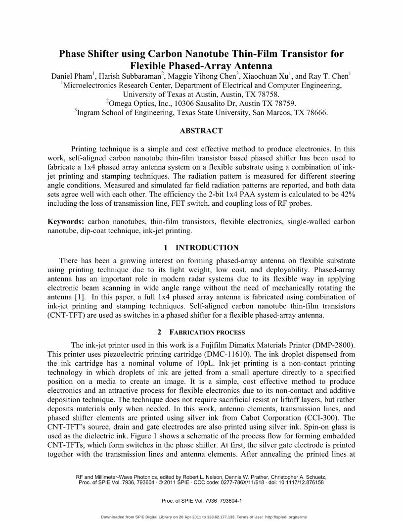
Daniel Pham1, Harish Subbaraman2, Maggie Yihong Chen3, Xiaochuan Xu1, and Ray T. Chen1 1Microelectronics Research Center, Department of Electrical and Computer Engineering,
University of Texas at Austin, Austin, TX 78758. 2Omega Optics, Inc., 10306 Sausalito Dr, Austin TX 78759.
3Ingram School of Engineering, Texas State University, San Marcos, TX 78666.
ABSTRACT
Printing technique is a simple and cost effective method to produce electronics. In this work, self-aligned carbon nanotube thin-film transistor based phased shifter has been used to fabricate a 1x4 phased array antenna system on a flexible substrate using a combination of ink-jet printing and stamping techniques. The radiation pattern is measured for different steering angle conditions. Measured and simulated far field radiation patterns are reported, and both data sets agree well with each other. The efficiency the 2-bit 1x4 PAA system is calculated to be 42% including the loss of transmission line, FET switch, and coupling loss of RF probes.
Keywords: carbon nanotubes, thin-film transistors, flexible electronics, single-walled carbon nanotube, dip-coat technique, ink-jet printing.
1 INTRODUCTION There has been a growing interest on forming phased-array antenna on flexible substrate
using printing technique due to its light weight, low cost, and deployability. Phased-array antenna has an important role in modern radar systems due to its flexible way in applying electronic beam scanning in wide angle range without the need of mechanically rotating the antenna [1]. In this paper, a full 1x4 phased array antenna is fabricated using combination of ink-jet printing and stamping techniques. Self-aligned carbon nanotube thin-film transistors (CNT-TFT) are used as switches in a phased shifter for a flexible phased-array antenna.
2 FABRICATION PROCESS
The ink-jet printer used in this work is a Fujifilm Dimatix Materials Printer (DMP-2800). This printer uses piezoelectric printing cartridge (DMC-11610). The ink droplet dispensed from the ink cartridge has a nominal volume of 10pL. Ink-jet printing is a non-contact printing technology in which droplets of ink are jetted from a small aperture directly to a specified position on a media to create an image. It is a simple, cost effective method to produce electronics and an attractive process for flexible electronics due to its non-contact and additive deposition technique. The technique does not require sacrificial resist or liftoff layers, but rather deposits materials only when needed. In this work, antenna elements, transmission lines, and phased shifter elements are printed using silver ink from Cabot Corporation (CCI-300). The CNT-TFT’s source, drain and gate electrodes are also printed using silver ink. Spin-on glass is used as the dielectric ink. Figure 1 shows a schematic of the process flow for forming embedded CNT-TFTs, which form switches in the phase shifter. At first, the silver gate electrode is printed together with the transmission lines and antenna elements. After annealing the printed lines at
RF and Millimeter-Wave Photonics, edited by Robert L. Nelson, Dennis W. Prather, Christopher A. Schuetz,Proc. of SPIE Vol. 7936, 793604 · © 2011 SPIE · CCC code: 0277-786X/11/$18 · doi: 10.1117/12.876158
Proc. of SPIE Vol. 7936 793604-1
Downloaded from SPIE Digital Library on 20 Apr 2011 to 128.62.177.133. Terms of Use: http://spiedl.org/terms

160oC for 10 minutes, a spin-on glass dielectric material is printed on top of the gate electrode and annealed. Then, the silver source and drain (same width as transmission line which is 300 μm) electrodes are printed with the gate length of 100μm. After annealing, wet silver droplets are printed on the source drain areas to provide a good contact between source drain electrodes with CNT film, which is captured by a special thin Kapton layer with adhesive on one side. The self-aligned CNT film is formed by using a dip-coat technique on sacrificial silicon substrate as discussed in reference [2].
Figure 1: Schematic of bottom gate integration for our CNT-TFT which acts as a switch for the phased shifter.
III. Design of 2-bit 1x4 PAA system In this work, standard microstrip antenna design techniques are used to design the
transmission lines, antenna elements and coplanar waveguide to microstrip line transition sections [3-10]. Figure 2 shows the layout of the 2-bit 1x4 element phased array antenna subsystem that has been designed and fabricated. The RF signal is applied through the RF input coupling section. The signal is then split into two branches, with each branch split further into two more sub branches, thus giving a total of 4 branches with equal length. Each of the 4 branches feed a phase shifting network, which usse CNT-TFTs as switches. The outputs from the phase shifters are connected to the antenna elements.
Proc. of SPIE Vol. 7936 793604-2
Downloaded from SPIE Digital Library on 20 Apr 2011 to 128.62.177.133. Terms of Use: http://spiedl.org/terms

1
2
3
4
5
6
7
8
9
10
11
12
13
14
15
16
: 0.785cm
: 1.57cm
1
2
3
4
5
6
7
8
9
10
11
12
13
14
15
16
: 0.785cm
: 1.57cm
Figure 2: Schematic representation of a 2-bit, 1x4 PAA system. By controlling the ON/OFF ratio of the CNT-TFT switches in the phase shifting network, the phase of the RF signal feeding the antenna elements is controlled.
Table 1 shows the switching pair selection for the phase shifter versus steering angle for the designed PAA system. Switch numbers are shown on Figure 2. By controlling the ON/OFF ratio of the switch pairs as indicated in Table 1, beam steering at -27 o, 0 o, 27 o, and 45o is achieved. This PAA system is designed for operation at 5GHz (C-band).
45o2.355cm1, 25, 7
0o01, 25, 69, 1013, 14
-27o-0.785cm3, 45, 8
10, 1113, 14
27o0.785cm1, 26, 79, 1215, 16
Steering Angle
Length difference between adjacent
elements
Switch Pair Selection
45o2.355cm1, 25, 7
0o01, 25, 69, 1013, 14
-27o-0.785cm3, 45, 8
10, 1113, 14
27o0.785cm1, 26, 79, 1215, 16
Steering Angle
Length difference between adjacent
elements
Switch Pair Selection
Table 1: Switch pair selection versus steering angle for the 5GHz 2-bit 1x4 PAA system
IV. Multilayer Metal Interconnection Multilayer metal interconnect is also developed to provide connection to the gate electrodes from an external power supply. A thin Kapton (25μm) substrate with adhesive coating on one side is bonded on top of the first substrate containing the printed PAA subsystem. Contact vias are formed prior to attaching in order to obtain metal contacts with the gate contact pads on the first substrate. A pressurized annealing process on a heat chuck at 100oC is used to bond these layers together. Then, silver ink is printed on the top layer to form the metal connection lines. The liquid silver ink is printed one or multiple times to fill the contact vias, which makes contact between the bottom gate contact pads and top interconnection lines. Another annealing process is performed in order to evaporate the remaining solvent in the silver solution to form solid silver filled contact vias. Figure 3 shows a picture of the fully fabricated 2-
2-bit phase shifter
Antenna Element
CNT-TFT Switch
RF input
Proc. of SPIE Vol. 7936 793604-3
Downloaded from SPIE Digital Library on 20 Apr 2011 to 128.62.177.133. Terms of Use: http://spiedl.org/terms

bit, 1x4 PAA system on a Kapton substrate. Notice that a third thin Kapton layer is applied on top of the second layer to protect the metal interconnection lines and vias, thus acting as an encapsulating layer. Probing pads are formed using double-sided copper tape.
Figure 3: Picture of a complete 2-bit 1x4 PAA system containing CNT-TFTs as switches in the phase shifting network. Multilayer metal interconnection produces a fully packaged system with metal interconnection lines.
3 EXPERIMENTAL SET UP AND DATA The PAA far-field radiation pattern is measured using the measurement setup shown in Figure 4. Te figure shows the entire measurement setup with the network analyzer, receiving horn and microwave spectrum analyzer (MSA). The RF signal from a HP8510C network analyzer is applied to the input of the PAA system. The PAA system is spread out flat on a thick flexi glass substrate. The stage is built on flexi glass so it can also be used to perform bending experiments in order to study the influence of bending on far-field patterns. The entire circuit is mounted vertically on a precision rotation stage along with the DC and RF probes. The CNT-TFT switch network is controlled using a mainframe computer with a switch control module. As shown in Table 1, for each steering angle, 8 CNT-TFT switches are controlled corresponding to each desired steering angle. RF absorbers are arranged around the PAA setup in order to eliminate multi-path effects. The radiated signal is received by a receiving horn antenna which is connected to a microwave spectrum analyzer (MSA). The received power is measured on the MSA as a function of the rotation angle, thus producing the far field patterns.
Proc. of SPIE Vol. 7936 793604-4
Downloaded from SPIE Digital Library on 20 Apr 2011 to 128.62.177.133. Terms of Use: http://spiedl.org/terms

Figure 4: a) Experimental setup to measure the far-field radiation pattern of the printed 1x4 PAA system, b) Close up picture showing the 1x4 PAA system. The radiation pattern for a 5.31GHz signal is collected using the above setup. All the four azimuth steering angles are measured. Figure 5 shows the measured and simulated far field radiation patterns of the PAA system at 0 degree and -27 degree steering angles. Two different set of PAAs are used for the measurement. The measured points are indicated by data points whereas the simulated patterns are shown as smooth curves. It can be seen from the results that the measured and simulated far field patterns agree very well with each other.
a)
-60 -40 -20 0 20 40 60
0
Nor
mal
ized
Pow
er (d
B)
Steering Angle (Degrees)
Simulation (0 degree) Exp. data #1 Exp. data #2
b)
-60 -40 -20 0 20 40 60
-10
0
simulation (-27 degree) Exp data #1 Exp data # 2
Nor
mal
ized
Pow
er (d
B)
Steering Angle (Degrees)
Figure 5: Measured and Simulated Far-Field Radiation Patterns of the Printed PAA system at a) 0 degrees and b) -27 degree.
The efficiency the 2-bit 1x4 PAA system is calculated to be 42% including the loss of transmission line, FET switch, and coupling loss of RF probes.
4 SUMMARY A 2-bit, 1x4 phased-array antenna system on Kapton substrate has been designed and
fabricated on lightweight and flexible substrate. CNT-TFT is used as a switch in the phase shifting network. Beam steering of a 5.31GHz signal from 0o to -27o has been demonstrated. This light weight, flexible and conformal PAA has an efficiency of 42%, and it is a good candidate for portable wireless system to meet challenging requirements.
REFERENCES [1] Li-Ron Zheng, Majid Nejad, Sual Rodriguez, Lu Zhang, Cairong Chen, Hannu Tenhunen,
System-on-flexible substrates: Electronics for future smart-intelligent world. Proceeding of HDP 2006 IEEE, pg 29-36.
[2] Daniel Pham, Harish Subbaraman, Maggie Yihong Chen, Xiaochuan Xu, Ray T. Chen, Bending Tests of Carbon Nanotube Thin-Film Transistors on Flexible Substrate, SPIE
Proc. of SPIE Vol. 7936 793604-5
Downloaded from SPIE Digital Library on 20 Apr 2011 to 128.62.177.133. Terms of Use: http://spiedl.org/terms

Conference 2010 on Carbon Nanotube, Graphene, and Associated Devices III, Vol. 7761, pg. 7761-7725
[3] Mailloux, R.J., Phased Array Antenna handbook, Artech House Inc., 1994 [4] K.R.Carver and J.W. Mink, “Microstrip Antenna Technology,” IEEE Trans. Antenna
propagation, vol. AP-29, no. 1, pp 2-24, Jan. 1981. [5] M. LeMieux, M. Roberts, S. Barman, Y. W. Jin, “Self-Sorted, Aligned Nanotube Newworks
for TFT,” Science, Vol. 321, pp. 101-104, 2008. [6] Bhartia P., et al. Millimeter-Wave Microstrip and Printed Circuit Antennas. Norwood, Mass.
Artech House 1991. [7] James J.R., P.S.Hall and C. Wood. Microstrip Antenna Theory and Design. London, United
Kingdom, Peter Peregrinus 1981. [8] Brian C Wadell, Transmission Line Design Handbook , Artech House 1991. [9] D. Pavlidis and H. L. Hartnagel, “The design and performance of three-line microstrip
couplers,” IEEE Trans. On Microwave Theory and tech., Vol. 24, No.10, pp. 631-640, Oct. 1976
[10] Gildas P. Gauthier, etc, “W-band Finite Ground Coplanar waveguide (FGCPW) to Microstrip Line Transition,” IEEE MTT-S Digest, TU2E-3, pp. 107-109, 1998
Proc. of SPIE Vol. 7936 793604-6
Downloaded from SPIE Digital Library on 20 Apr 2011 to 128.62.177.133. Terms of Use: http://spiedl.org/terms