compact phase shifter design using barium strontium...
TRANSCRIPT
UNIVERSITY OF CALIFORNIA
Santa Barbara
Compact Phase Shifter Design Using Barium Strontium Titanate
Thin-Film Varactors
A Thesis submitted in partial satisfaction of the
requirements for the degree of Master of Science
in Electrical and Computer Engineering
by
Justin Lee Serraiocco
Committee in charge:
Professor Robert A. York, Chair
Professor Umesh K. Mishra
Professor James S. Speck
September 2003
The thesis of Justin Lee Serraiocco is approved.
James S. Speck
Umesh K. Mishra
Robert A. York, Committee Chair
August 2003
ABSTRACT
Compact Phase Shifter Design Using Barium Strontium Titanate
Thin-Film Varactors
by
Justin Lee Serraiocco
Phase shifters are important components in many microwave subsystems
used for radar and communication. Current technology makes phase shifters
very costly, and inhibits widespread adoption of devices such as phased-array
antennas. Barium strontium titante (BST) thin-film varactor technology en-
ables the creation of low cost analog phase shifters. Research is presented
here that describes how to further decrease the cost of BST phase shifter
modules by use of lumped element inductors and high impedance transmis-
sion lines. Most notably, a X-band reflection-type phase shifter using BST
varactors achieved 250 of phase shift while measuring only 0.36mm2.
iii
Contents
1 Introduction 1
1.1 Analog versus Digital . . . . . . . . . . . . . . . . . . . . . . . 2
1.2 Current Phase Shifter Technology . . . . . . . . . . . . . . . . 3
1.3 New Phase Shifter Technologies . . . . . . . . . . . . . . . . . 4
1.3.1 MEMS . . . . . . . . . . . . . . . . . . . . . . . . . . . 4
1.3.2 RF CMOS . . . . . . . . . . . . . . . . . . . . . . . . . 5
1.3.3 LTCC . . . . . . . . . . . . . . . . . . . . . . . . . . . 6
1.3.4 Integrated BST passives . . . . . . . . . . . . . . . . . 6
2 Integration of Passives and BST Thin-films 8
2.1 Component Modeling . . . . . . . . . . . . . . . . . . . . . . . 9
2.2 Process Flow . . . . . . . . . . . . . . . . . . . . . . . . . . . 11
3 Reflection-Type Phase Shifters 15
3.1 Distributed versus Lumped . . . . . . . . . . . . . . . . . . . . 16
3.2 Resonator Loads . . . . . . . . . . . . . . . . . . . . . . . . . 18
3.3 Quadrature Hybrid Couplers . . . . . . . . . . . . . . . . . . . 19
3.4 X-band BST RTPS Designs . . . . . . . . . . . . . . . . . . . 21
3.4.1 Lange coupler based . . . . . . . . . . . . . . . . . . . 21
3.4.2 Lumped coupler based . . . . . . . . . . . . . . . . . . 23
3.4.3 Impedance transformed couplers . . . . . . . . . . . . . 27
iv
4 Distributed Analog Phase Shifters 34
4.1 Strategies for Size Reduction . . . . . . . . . . . . . . . . . . . 38
4.2 Synthetic Transmission Lines . . . . . . . . . . . . . . . . . . 39
4.3 High Impedance Coplanar Strip Transmission Lines . . . . . . 45
4.4 Comparisons . . . . . . . . . . . . . . . . . . . . . . . . . . . . 51
5 Conclusion 55
v
Chapter 1
Introduction
Phase shifter circuits are found in microwave systems such as phased-array
antennas and highly linear power amplifiers. In a phased-array antenna sys-
tem, phase shifters are used to electrically control the output beam direction.
In power amplifiers, phase shifting feedback networks are used to compensate
for AM-PM distortion and other nonlinearities. Without phase shifters, an
electrically scanned array antenna could not be built; a physically rotating
directional antenna would have to be used. Enhanced efficiency power am-
plifiers can be built without phase shifters, but might have to use techniques
such as baseband predistortion, which require more hardware support. The
phase shifter is a crucial device for realizing these two types of circuits, and
many others.
One might be led to believe from the above description that the phase
shifter is a device complicated in operation and design. However, quite the
opposite is true. The phase shifter is a two-port device, whose sole respon-
sibility is alter an input signal’s relative phase according to a control signal.
Ideally, this task would be accomplished with no attenuation. The design
of the phase shifter can be as simple as connecting four quarter-wave trans-
mission lines with a pair of varactor diodes. However, more efficient designs
require a bit more thought.
1
1.1 Analog versus Digital
One of the primary characteristics of a phase shifter is the nature of its control
signal. Analog phase shifters have a single analog input control voltage,
giving infinite resolution theoretically. Digital phase shifters have n digital
input signals offering a resolution limited by the least significant bit. For
a 4-bit digital phase shifter, this is typically 22.5. Both types have their
advantages and drawbacks, and are suited for different purposes.
Digital phase shifters require switches capable of passing microwave sig-
nals to function. The switches can be realized electromechanically, or with
solid-state technology such as pin diodes or FETs. Obtaining higher phase
shift resolution with digital phase shifters generally requires the addition of
more control bits. As is the case with all digital circuits, they are generally
less sensitive to power supply and temperature variations than their analog
counterparts.
Most analog phase shifters rely on a voltage variable capacitance, or var-
actor, to function. Varactors also can be implemented electromechanically,
with diodes, or with ferroelectric films. Using a single analog control volt-
age, it is possible to obtain very precise phase shifts. Unlike digital designs,
analog designs are very sensitive to process variations and their operating
environment.
Analog phase shifters are a natural fit for linearized power amplifiers. The
error detection circuits in feedforward and feedback amplifiers output analog
signals. These voltages can be sent directly to an analog phase shifter, which
corrects the input or output signal. Using a digital phase shifter here would
require adding an analog to digital converter. The limited resolution of most
digital phase shifters also makes them a poor fit for linearization circuitry.
Phased-array antenna systems are usually computer controlled, and hence
2
output digital control signals. When analog phase shifters are used, each
must be paired with a digital to analog converter. Digital phase shifters do
not require this additional circuitry, and may be more suitable for array pur-
poses. A few other considerations must be taken into account when deciding
the more appropriate phase shifter type. For example, the single control volt-
age of the analog phase shifter reduces the wiring complexity on the surface
of the array compared to a digital implementation.
1.2 Current Phase Shifter Technology
Traditionally, phase shifters for phased-array antenna systems have been im-
plemented with ferrites. These devices have evolved over the last few decades
to become smaller, less lossy, and more power efficient. There are a variety
of different designs offering high performance, but all share a common draw-
back. In order to tune the ferrite material, strong magnetic fields must be
generated. This is most commonly done with coils requiring bias voltages
in the hundreds to thousands of volts. Ferrite phase shifters are also very
slow, requiring long tuning times. Most ferrite phase shifter designs are not
amenable to mass production methods, which keep their unit costs very high.
Phased-arrays implemented with ferrite phase shifters are not cost-effective
for terrestrial commercial applications.
The maturation of GaAs MESFET technology over the last decade has
made feasible the creation of all solid-state phased-arrays. GaAs MMIC
technology offers the broadest range of options for the creation of phase
shifter circuits. Both varactors and switches are available, enabling analog
and digital designs. Both distributed and lumped components are available
as well. The only drawback of MMIC technology is cost. In the past, with
the military as their only customer, MMIC designers have not been very
sensitive to cost considerations. With the recent explosion in commercial
3
and consumer wireless products, more cost effective phase shifter designs
have begun to emerge. The increased market for MMIC devices has also
reduced fabrication costs.
1.3 New Phase Shifter Technologies
Even though GaAs MMIC technology continues to mature, with yields and
wafer diameters increasing continuously, they are still a costly option for
the microwave design engineer. Several research technologies are receiving
attention as potential candidates to supply phase shifters for cost sensitive
markets. Most of these technologies can be applied to reduce the costs of
other types of microwave circuits as well. Most of these technologies are
capable of reducing the cost of microwave phase shifters to a fraction of their
current prices, and some can offer higher performance as well.
1.3.1 MEMS
MEMS (micro-electro-mechanical systems) technology uses advanced thin-
film processing techniques to realize miniaturized mechanical systems. Both
switches and varactors can be realized using multiple metal layers and care-
fully controlled etchings. The process flow usually involves temperatures
below 200C, and is therefore compatible with standard semiconductor pro-
cessing. This potentially allows integration with GaAs MMIC or CMOS
technologies. The advantages of MEMS for phase shifters is low loss and
low parasitics. MEMS switches are capable of routing very high frequency
microwave signals with very little loss. MEMS varactors use air or vacuum
as their dielectric, and have negligible leakage as a result. Carefully designed
devices can function up to 100 GHz, rivaling the best semiconductor tech-
nologies. These attributes make MEMS technology attractive for low loss
and high frequency applications.
4
A drawback of MEMS technology for phase shifter implementation is the
large number of processing steps. Since it uses the standard lithographic
tools of the semiconductor industry, the costs are similar. A MEMS switch
process can exceed fifteen mask layers, making processing costs high. An
additional problem with MEMS technology is packaging. The thin metal
membranes functioning as switching elements or varactors are very sensitive
to their environment, and must be packaged in either an inert or vacuum
environment. Hermitic packaging increases cost and makes the device more
bulky. It also reduces the potential for integration with other circuit compo-
nents. Another drawback are the large control voltages required. Reduction
of these voltages results in increased phase noise and device fragility. Typical
voltages for robust operation are in the range of 80 to 100 volts.
1.3.2 RF CMOS
A decade ago, the use of CMOS technology for microwave circuits would have
been considered unthinkable. However, the continual scaling of CMOS tran-
sistors to smaller dimensions and higher frequencies have made CMOS a vi-
able technology for microwave circuits. A number of variations on the CMOS
process, including BiCMOS using silicon-germanium HBTs and silicon on in-
sulator technology, extend the power and frequency handling capabilities of
CMOS even higher. With huge investments in technology and infrastructure
from the digital IC business, CMOS can be an attractive proposition for
high volume microwave and mixed-signal integrated circuits. However, the
high costs of prototyping circuits in leading-edge CMOS technology makes
development costs very high. The necessity of ’first-time-right’ design, driven
principally by high masks costs, increases development time and makes de-
sign revisions very costly. For low and moderate volume applications, RF
CMOS may not be feasible.
5
1.3.3 LTCC
Low temperature cofired ceramic technology uses multiple layers of insulating
ceramics together with metallic pastes to realize microwave circuits. It allows
a three-dimensional integration aspect not feasible with thin-film multilayer
technologies. The metallic pastes can be high conductivity, for realizing
transmission lines, inductors, and capacitor plates, or low conductivity, for
integrated resistors. Different types of ceramics can also be integrated to-
gether. Higher dielectric constant thin layers for realizing capacitors, or low
dielectric constant thick layers to reduce parasitic coupling. More recently,
the integration of ferroelectric, piezoelectric, and ferrite ceramic layers has
been accomplished. This allows the creation of tunable microwave compo-
nents, such as phase shifters, directly within the LTCC structure. More
conventionally, it is also possible to integrate semiconductor components on
the surface or within a cavity of the LTCC stack. The integration of arbitrary
types of transistors and diodes for gain, switching, and tuning makes LTCC
technology very flexible. LTCC technology uses lower resolution lithogra-
phy than is necessary for MEMS or CMOS technologies. Overall, LTCC
technology seems very promising for realizing low cost and highly integrated
microwave circuits. The technology is relatively new, and is just beginning
to reach widespread usage.
1.3.4 Integrated BST passives
The technology explored in this thesis is the integration of barium strontium
titanate (BST) with traditional thin-film passive technology. The passives
are implemented with conventional semiconductor processing techniques on
dielectric substrates. Processing thin-film passives is less costly than MMIC
and CMOS processes, since the tolerances are greater and the substrates
are cheaper. Resistors, capacitors, inductors, and transmission lines can
6
be integrated onto a substrate in a simple process. When these passives
are integrated with flip-chip or wirebonded active components, the resulting
device is sometimes referred to as a multi-chip-module (MCM). This process
is capable of creating high performing, compact circuits. Circuit sizes and
external component counts need to be kept to a minimum to ensure economic
feasibility. The addition of a thin-film varactor technology to a passives
process can help achieve this. By integrating varactors, only gain and switch
stages need to be added as discrete devices to complete the functionality a
module. Analog phase shifters can be created without using any external
components. Extremely low cost phase shifters can then be realized with
proper circuit design to minimize circuit size. Some of the designs explored
here can also be implemented in other technologies, but the low cost nature
of the integrated BST process may make it the most appropriate for realizing
low cost microwave phase shifters circuits.
7
Chapter 2
Integration of Passives andBST Thin-films
The goal of integrating passive thin-film components with a BST varactor is
to allow the development of extremely low-cost tunable microwave compo-
nents. At lower microwave frequencies, distributed circuit design techniques
cannot be used because they result in uneconomically large circuit sizes.
Lumped element design must be scaled up in frequency to function at fre-
quencies up to around 10 GHz. The integration of a low cost, high performing
varactor with spiral inductors, transmission lines, capacitors, and resistors is
key to this effort.
Current varactor circuit elements vary in loss and tunability. Hyper-
abrupt pn junction diodes can have tuning ratios in excess to 10:1, but can
become very lossy with tuning. MEMS varactors have typical tunabilities of
less than 1.5:1, but with extremely low loss, even deep into the millimeter-
wave region. To maintain reasonable losses with a moderate Q technology at
typical microwave frequencies, a tuning ratio of at least 2:1 is essential. Lower
tuning ratios greatly increase the difficulty of realizing design objectives,
necessitating the cascade of multiple stages. This increases the overall circuit
size and reduces performance.
The BST material was grown on c-plane sapphire substrates using rf
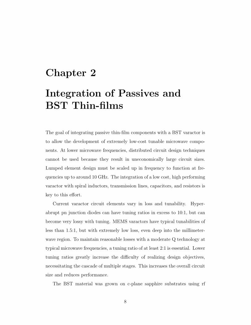
8
Figure 2.1: The BST varactor circuit model.
magnetron sputtering. The initial setup and materials costs for a sputtering
system are much lower than those of other deposition technologies, such as
MOCVD or MBE. The films were sputtered from multiple ceramic targets
consisting of varying ratios of barium and strontium. A 50:50 ratio would
give films of higher tunability, but a 30:70 film would have less loss, and a
higher breakdown voltage. Application of a dc bias voltage to the capacitor
alters the dielectric constant, resulting in a capacitance change. Initial design
optimistically assumed a 3:1 tuning ratio. Later designs assumed a more
realistic 2.5:1 or 2:1 ratio.
2.1 Component Modeling
The BST deposition system was used primarily for material science research,
and consistency was difficult to obtain. Variations in the dielectric constant,
tuning range, and loss were encountered from growth to growth. It was
difficult to take into account all of these variations in a design. Constructing
an accurate model of the BST varactor posed a serious challenge. The basic
circuit model is shown in figure 2.1. The series resistor represents electrode
loss, and the parallel RC circuit represents the capacitance and the dielectric
loss.
Attempting to characterize the electrode losses in the parallel plate var-
actor structure proved very difficult. The thin metal layers and small dimen-
9
sions rendered standard treatments of the ohmic loss inaccurate. Extraction
of data directly from test structures was attempted. Data accurate enough
for use in models was difficult to obtain due to measurement uncertainty
and variations in individual devices. Attempts to extract the dependence
of electrode loss on parameters such as length, width, and gap through a
comprehensive set of test structures failed. It was difficult to correlate the
extracted values with the simple three element circuit model. The varactor
structure was also simulated in a full wave finite element electromagnetic
simulator. It again proved difficult to extract circuit model data from the
simulations. However, a correlation was made between higher Q and a wider,
shorter capacitor structure. This went against the previously held belief that
a long, skinny electrode was better. Both EM simulations and fabricated
device measurements indicated that a wider structure had less ohmic loss.
Assigning a value to the capacitor in the circuit model was a simple
matter. Obtaining the correct capacitance in the fabricated circuit proved
to be more difficult. Initially, no fringing capacitance was assumed to be
present. Later, analysis indicated that there was approximately a twenty
percent increase in capacitance due to fringing. This fringing capacitance
reduces the tunability of the varactor, and it is desirable to minimize it. For
a given area, the shape with the smallest periphery is a square. Since fringing
is proportional to periphery, the square is the ideal capacitor shape. Using
formulas adapted from [?], a synthesis procedure was developed to obtain
the desired zero bias capacitance using a square capacitor.
Dielectric loss measurements are a simple latter at 100 MHz, but are con-
siderably more complicated at 10 GHz. The test structures accommodating
the varactor and the high frequency coplanar probe made extracting accurate
data difficult. Measurement of a small capacitor at high microwave frequen-
cies stressed the accuracy of the test equipment. An additional complication
10
was variation of the loss with bias. There was no attempt made to account
for this variation.
The inaccuracy of closed form spiral inductor models is well known. An
addition complication beyond modeling the inductive and resistive contribu-
tion is modeling the coplanar capacitive components. Most published works
assume an ground beneath the substrate, and use the simple parallel plate
capacitance formula. There is only a single treatment of coplanar ground ca-
pacitance [?]. Even that is only a simplistic model, approximating the spiral
traces and grounds as asymmetric coplanar strip transmission lines. Using
electromagnetic simulation to account for finite metal thickness increased
simulation times ten fold.
2.2 Process Flow
The lengthy high temperature BST sputter deposition process dictated that
the initial step in the process had to be the fabrication of the varactor struc-
ture. This is beneficial because it allows the optimal processing of the varac-
tor without regard to damage to other circuit components. However, the fer-
roelectric material is itself very sensitive to the subsequent processing steps.
Oxygen plasma cleaning, for example, could significantly change the dielec-
tric constant of the deposited material. The sensitivity of BST to hydrogen
gas meant that PECVD deposition of silicon nitride was not an option. The
oxygen plasma cleaning was kept to a minimum, but was sometimes in-
evitable when lithographic mistakes were made. The restriction on PECVD
prevented a quick and easy method to passivate the varactors.
The first step in processing the BST varactors was deposition of the bot-
tom electrode. As mentioned previously, only electrode materials capable of
withstanding the high growth temperatures could be considered. Unfortu-
nately this rules out most high conductivity metals, leaving platinum as the
11
best option. After depositing a thin layer of titanium for adhesion, 200nm of
platinum was deposited via e-beam. The restriction on the thickness of this
layer came from the structure of the overlay BST capacitor. The dielectric
layer needs to be thicker than the bottom electrode to prevent a short circuit
when the top electrode was deposited. The BST layer was limited to ap-
proximately 300nm, since growth times longer than three hours excessively
degraded the films. This thickness resulted in a relative dielectric constant of
approximately 450, giving a capacitance density of 15fF/µm2. This density
was about the highest that could be tolerated, given the operating frequencies
chosen, and the contact lithography methods used. Platinum is not easily
etched, so a liftoff technique was used.
After growth in the sputtering system, the BST was wet etched in a
solution of hydroflouric acid. Different samples had vastly different etch
rates and uniformity. Depending on the condition of the growth chamber, a
tough interfacial layer could be formed at the bottom electrode. This layer
often proven impossible to etch through, necessitating that the process be
started again from scratch.
Normally, the top electrode was deposited at this stage. However, when
high valued biasing resistors were integrated into the process, it was neces-
sary to deposit it first. A 40nm thick layer of nichrome was used as the
resistor material. This material’s resistivity is not that large, and the 5kΩ
resistors needed had to be made very narrow and meandered to meet both
the resistivity and size requirements. The deposition of a thick top electrode
prior to resistor deposition prevents high resolution contact lithography due
to planarity issues. Therefore, the nichrome material deposited via e-beam
first. The thinness of this layer did not interfere with the resolution of the
top electrode layer. The composition of this electrode varied, but usually
consisted of a 100nm platinum layer capped with a 500nm gold layer, both
12
deposited via e-beam and lifted-off.
Once the varactors and resistors were fabricated, two thick gold layers
were deposited for the coplanar transmission lines, interconnects, spiral in-
ductors, and air-bridges. The first gold layer measured one micron thick,
and was the primary trace layer. Then, a thick resist impervious to normal
solvents was deposited for the air-bridge support. A second one micron gold
layer was then deposited to form the bridge. To create thicker gold spirals
without developing complicated liftoff stacks, backside lithography, or elec-
troplating, the second gold layer was sometimes selectively layered onto the
base spiral inductor metalization, doubling the thickness in most places. A
gap was kept between the air-bridges and this thicker layer to prevent short-
ing. The fabricated circuits were tested using on-wafer coplanar probes and
a network analyzer. For further details on the BST overlay varactor device
and process, consult [1].
13
Bibliography
[1] B. Acikel, ”High Performance Barium Strontium Titante Varactor Tech-
nology for Low Cost Circuit Applications,” Ph.D thesis, University of
California, Santa Barbara, 2002
14
Chapter 3
Reflection-Type Phase Shifters
The reflection-type phase shifter (RTPS) is simple phase shifter design that
uses a minimal number of components. It is most commonly realized in
analog form, with a single input control voltage. The RTPS can be realized in
many different forms, but all include a quadrature coupler and dual, identical
reflective loads. The reflective loads are one-port circuits with variable phase
reflection characteristics. The quadrature coupler’s function is to isolate the
input and output signals, turning the phase shifting behavior of the reflective
load into more usable two-port device.
The reflective load responsible for the phase shift can be realized in many
different ways. The simplest is to use a tunable shunt capacitor. Real-
izing larger amounts of phase shift requires resonating the capacitor with
an inductor or quarter-wave transmission line section. The technique most
appropriate depends on the technology used to implement the phase shifter.
Variables such as loss and size must also be taken into account when deciding
on a reflective load topology.
Equal in importance to the reflective load is the circuit which separates
the input signal from the reflected output signal. The ideal circuit would
contain three ports, one each for the input signal, reflection load, and output
signal, and have appropriate isolation between the ports. Such a device,
15
called a circulator, requires the use of bulk ferrite materials and is not easily
integrated into a microwave IC. A workable alternative is to use a four-
port device. A reciprocal four-port circuit with the appropriate isolation
properties can be realized in thin-film form, and is termed a quadrature
hybrid coupler. The coupler divides an input signal from any port into the
two opposite ports, while isolating the adjacent one. In order to obtain
the expected behavior, two reflection loads must be included in the RTPS,
connected to the coupled and thru ports of the hybrid. The RTPS’s phase
shifted input signal is found at the hybrid’s isolated port, and will ideally be
isolated from the RTPS input signal.
Proper selection of the form for the quadrature coupler and reflection
load is critical to obtaining the most effective RTPS design. Variables such
as operating frequency, cost, and size will determine the appropriate circuits
in any given process technology.
3.1 Distributed versus Lumped
When monolithic technology is used to realize a circuit, an important con-
sideration is minimization of die area. This can make the use of transmission
line components a costly proposition. At frequencies above 20 GHz, dis-
tributed components shrink to acceptably small sizes. The combination of
moderately high dielectric constants (εr > 10), wafer thinning, and thru-
wafer vias make microstrip transmission lines at high frequencies relatively
compact. Therefore, reflective load designs utilizing transmission lines are
an option in MMIC processes at high frequencies.
If thru-wafer vias are not available, uniplanar transmission lines such as
coplanar waveguide can be used. However, the effective dielectric constant of
a CPW transmission line is approximately (εr +1)/2, leading to transmission
line lengths nearly twice that of electrically equivalent microstrip lines. CPW
16
transmission lines are more costly in terms of die area than microstrip trans-
mission lines on identical substrates. Techniques exist for reducing trans-
mission line sections to shorter lengths. In [1], reduced length transmission
lines were realized using high impedances lines with shunt capacitors. This
technique produces transmission lines that appear nearly identical to those
using full length transmission lines, but only over a narrow bandwidth.
At lower microwave frequencies, even reduced length transmission line
components become very long, and lead to unreasonably large dies if used.
The use of integrated thin-film lumped components, such as spiral inductors
and metal-insulator-metal (MIM) capacitors, becomes necessary to achieve
smaller die areas. This requires the addition of air-bridge and dielectric depo-
sition steps to a simple passive circuits process. These additional processing
steps increase processing complexity and reduce yield, increasing costs. The
payoff is greater flexibility in circuit design.
A concern with lumped thin-film components is maintaining a high qual-
ity factor, or Q. Distributed circuit components are usually assumed to have
Q of 200. Lumped components can be substantially lower. One of the main
concerns is maximizing spiral inductor Q. The insulating nature of typical
microwave IC substrates eliminates many causes of low Q in found in sili-
con processes, but getting large Qs can still be a challenge. The principle
method of raising Qs is to use thick metalization layers, with high conductiv-
ity metals such as copper. The skin and current crowding effects [?] limit the
effectiveness of using very thick metal layers. Poor closed-form models for
planar spiral inductors further increase the challenge of realizing high Q. Op-
timization via electromagnetic simulation is a must for maximizing inductor
quality factors.
17
3.2 Resonator Loads
Much of the literature on reflection-type phase shifter reflective loads fo-
cuses on distributed approaches using high tunability varactor diodes. This
makes it a challenge to discern whether an approach is feasible for compact
realization with limited tuning BST varactor.
The simplest reflective load is a single shunt capacitor. This approach
can be highly effective when the phase shift necessary is not large, or hyper-
abrupt tuning diodes are available. In [2], equation (3.1), was given to de-
scribe the phase shift behavior of a such a reflective load. rC represents the
tuning ratio of an ideally selected varactor, and is greater than one.
∆φ = 2(arctan(√
rC) − arctan(1√rC
)) (3.1)
Most MMIC varactors are limited to an rC of around four, and a corre-
sponding phase shift range of about 70. For BST technology with a tuning
range of about 2:1, this reduces to 40. The phase shift range required for
almost any application is usually greater than 90. Only varactor diodes
with special doping profiles are usually able to achieve large tuning ranges.
However, most of these devices have low Q. Therefore, the single varactor
technique is not that useful except in limited circumstances where loss is not
a huge concern or the required phase shift is small.
In [3], a technique is described for adding the admittances of two diodes
to double the phase shift. This was accomplished by using a λ/4 transmis-
sion line of an appropriate impedance. In [4], a reflective load consisting of
two separate varactor circuits resonating at different frequencies was used to
extend the phase shift range of low tuning varactors. Both of these tech-
niques are effective at increasing the phase shift range of a reflective load,
but are not appropriate for realizing compact phase shifters. The former
18
technique introduces a bulky quarter-wave transmission line, which is still of
significant size even when implemented with reduced-length high impedance
capacitively loaded lines. The latter technique uses two separate resonant
circuits, which will result in a large amount of insertion loss variation over
bias when implemented with components of low to moderate Q.
The only technique suitable for use in compact reflection-type phase
shifter circuits is the LC reflective load. Here, the variable capacitance of
the varactor is resonated with a series inductor. The appropriate design
equations are given in [2].
∆φ = 4 arctan(ZCv0
Z0
1
2(√
rC − 1√rC
) (3.2)
ZCv0 =1
ω0Cv0
(3.3)
Ll =ZCv0
2ω0
(√
rC +1√rC
) (3.4)
Equation (3.2) gives the maximum differential phase shift when a varactor
of center value Cv0 is connected in series with an inductor of value Ll, as
given by equation (3.4). This can increase the phase shift of limited tuning
varactors to useful values. Notice, however, than when rC is small, large
inductances and small varactor capacitances result. This places an upper
limit on the useful increase in phase shift possible with this technique.
3.3 Quadrature Hybrid Couplers
The function of the quadrature hybrid coupler in the reflection-type phase
shifter is to separate the input and reflected signal of the reflective load.
Network theory considerations dictate that a four port hybrid that splits the
input signal into two output ports, isolates the fourth port, and is reciprocal,
will have outputs in quadrature. This is not a concern for the RTPS, since
19
the phase difference is compensated for on the return trip through the hybrid
towards the output port.
A variety of designs for the quadrature hybrid coupler are possible. The
most basic is the branch-line hybrid [5]. This hybrid consists of four quarter-
wave transmission lines connected end to end in a loop. The transmission
lines are of different impedances, so that the thru and coupled ports remain
impedance matched to the input. The input signal splits in quadrature be-
tween the thru and coupled ports, is bounced off the reflective loads, and
recombines in phase at the isolated, or output port. This design is simple to
realize in microstrip form. In coplanar waveguide, airbridges are required at
the T-junctions to suppress moding. A total 12 air-bridges are required. The
use of quarter-wave lines is of concern for monolithic implementations below
20 GHz. The size reduction techniques of [1] can be used if high quality
shunt MIM capacitor are available. Even with heaving loading, the size of
this hybrid is considerable.
Taking the size reduction technique of [1] to its maximum, and using a
transmission line of infinite impedance transforms the transmission line into a
pure inductance. The pi-network approximation of a transmission line is well
known, and is used often to replace quarter-wave lines. The transformation of
the branch-line hybrid from distributed to lumped form is generalized in [6].
A simplified version of the transformation equations is given in [2]. The most
common lumped hybrid converts the four transmission line sections into two
inductors and six capacitors. This conversion is the most popular because
it minimizes the number of area consuming, and lossy, spiral inductors. Use
of the generalized equations in [6] allows an impedance transformation from
the input and output ports to the thru and coupled ports. This will allow
enhanced phase shift performance to be achieved, as explained later.
A third quadrature hybrid coupler is the Lange coupler [7]. Consisting of
20
four or more tightly coupled transmission lines, the Lange coupler exhibits
much wider bandwidth than branch-line or lumped couplers. It is also a
quarter wavelength long, but is very narrow in the other dimension. This
allows the Lange coupler to be bent in half, and reduced in length. The
Lange coupler is very popular in MMIC design even at lower frequencies,
because of its wide bandwidth and low loss. Its design more complicated
than either the branch-line or lumped couplers.
3.4 X-band BST RTPS Designs
A number of different reflection-type phase shifter designs were implemented
in the BST thin-film varactor process. A Lange coupler based design using an
LC reflective load was designed first. Although the Lange coupler is long, its
wide bandwidth allowed reasonable phase shifter performance to be obtained
even if the center frequency of the reflective load was miscalculated. This
could occur if either the inductor or BST dielectric constant was off in value.
Designs using only lumped elements were also fabricated. Although not
completely optimized in performance, these designs show promise for their
extremely compact size. All circuits were designed to operate at a center
frequency of 10 GHz.
3.4.1 Lange coupler based
The reflective loads for the Lange coupler based phase shifter was designed
according to the equations described above. The LC reflective load was
designed for a 180 phase shift at 10 GHz with a capacitance tuning ratio of
3:1. This resulted in a 1.6nH inductor and a 0.32pF zero bias varactor. This
inductance is near the upper limit of achievable values at 10 GHz, due to
self-resonant effects from capacitive parasitics. Its spiral had 2.5 turns, with
an outer diameter of 300µm, a conductor width of 25µm, and a conductor
21
-3
-2.5
-2
-1.5
-1
-0.5
0
8 9 10 11 12
Bias=0VBias=10VBias=20V
Lo
ss
(d
B)
Frequency (GHz)
Increasing Bias
Figure 3.1: Phase shift performance of X-band LC reflective load.
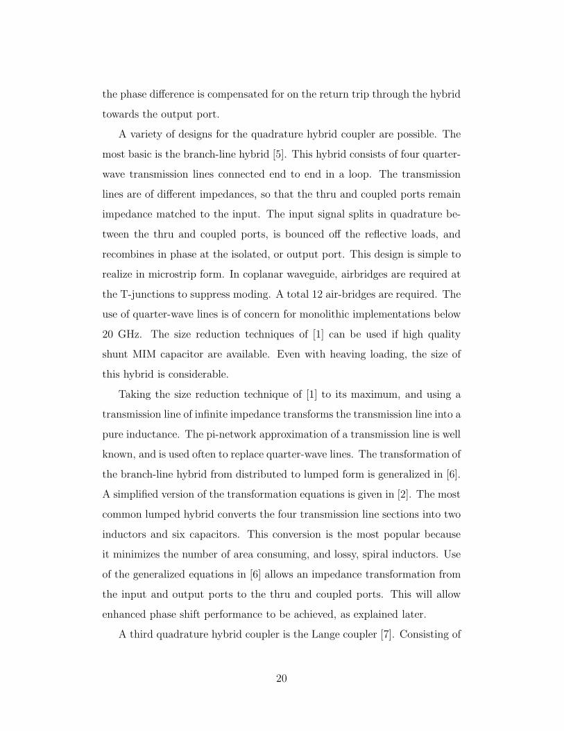
spacing of 12µm. The BST varactor dimensions were 4µm by 4µm.
The actual phase shift achieved with this load was only 100 at 10 GHz.
Further investigation revealed that the film capacitance density was approx-
imately 9fF/µm2 instead of the desired 15fF/µm2. In addition, the film
tunability was somewhat lower than the designed for 3:1 ratio. The reflec-
tive load exhibited a loss of -2.5dB at resonance, as seen in figure 3.1. This
was larger than expected, but good enough to obtain promising results when
integrated with the Lange coupler.
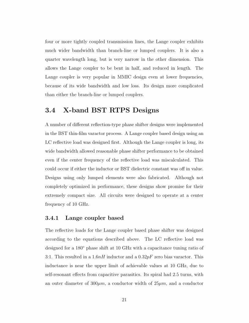
The Lange coupler was realized in a coplanar waveguide environment. Its
center frequency was 10 GHz, giving it a length of 3300µm and an overall
width of 650µm. The thru and coupled ports of the Lange coupler were
connected to a pair of the series LC resonators described above to complete
the phase shifter. The circuit is pictured in figure 3.2.
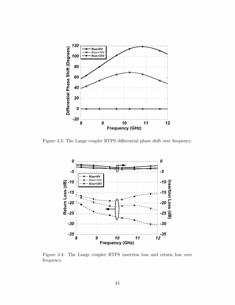
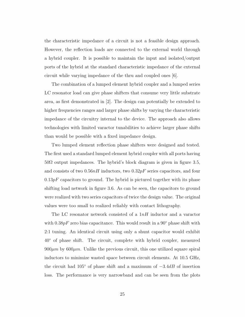
The Lange reflection phase shifter gave a maximum of 120 phase shift
22
Figure 3.2: The completed BST reflection phase shifter using a Lange cou-pler.
near 11 GHz. At this frequency, it had less than −3.3dB insertion loss for
all biasing conditions. For the 10 GHz to 12 GHz frequency range, it was
capable of over 100 phase shift with less than −4dB insertion loss. Over the
8 GHz to 12 GHz range it maintained greater than −15dB return loss. The
complete performance data are given in figures 3.3 and 3.4.
3.4.2 Lumped coupler based
Large valued spiral inductors have significant parasitics that give them low
self-resonant frequencies. The large dielectric constant of ferroelectric ma-
terial results in high capacitance densities, which in turn results in small
electrode areas. These two factors limit the achievable phase shift of a LC
series resonator using a low tunability varactor. The approach suggested
here is to utilize the degree of freedom given in equation (3.2) in choosing
the characteristic impedance. By choosing a smaller Z0, a smaller inductance
and a larger varactor capacitance result for a given phase shift. Smaller in-
ductances have fewer parasitics and higher self-resonant frequencies. The
inductors are also more compact. Due to the high dielectric constant of thin-
film BST, increased capacitance actually eases layout and makes the stray
parasitic capacitances less significant. The increase in electrode area is in-
significant compared to the scale of the overall circuit. Normally, changing
23
-20
0
20
40
60
80
100
120
8 9 10 11 12
Bias=0VBias=10VBias=20V
Dif
fere
nti
al
Ph
as
e S
hif
t (D
eg
ree
s)
Frequency (GHz)
Figure 3.3: The Lange coupler RTPS differential phase shift over frequency.
-35
-30
-25
-20
-15
-10
-5
0
-35
-30
-25
-20
-15
-10
-5
0
8 9 10 11 12
Bias=0V
Bias=10V
Bias=20V
Retu
rn L
os
s (
dB
) Ins
ertio
n L
oss
(dB
)
Frequency (GHz)
Figure 3.4: The Lange coupler RTPS insertion loss and return loss overfrequency.
24
the characteristic impedance of a circuit is not a feasible design approach.
However, the reflection loads are connected to the external world through
a hybrid coupler. It is possible to maintain the input and isolated/output
ports of the hybrid at the standard characteristic impedance of the external
circuit while varying impedance of the thru and coupled ones [6].
The combination of a lumped element hybrid coupler and a lumped series
LC resonator load can give phase shifters that consume very little substrate
area, as first demonstrated in [2]. The design can potentially be extended to
higher frequencies ranges and larger phase shifts by varying the characteristic
impedance of the circuitry internal to the device. The approach also allows
technologies with limited varactor tunabilities to achieve larger phase shifts
than would be possible with a fixed impedance design.
Two lumped element reflection phase shifters were designed and tested.
The first used a standard lumped element hybrid coupler with all ports having
50Ω output impedances. The hybrid’s block diagram is given in figure 3.5,
and consists of two 0.56nH inductors, two 0.32pF series capacitors, and four
0.13pF capacitors to ground. The hybrid is pictured together with its phase
shifting load network in figure 3.6. As can be seen, the capacitors to ground
were realized with two series capacitors of twice the design value. The original
values were too small to realized reliably with contact lithography.
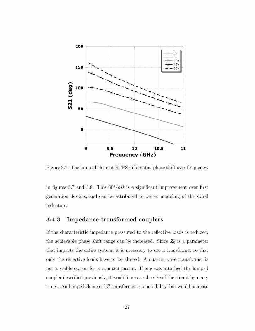
The LC resonator network consisted of a 1nH inductor and a varactor
with 0.38pF zero bias capacitance. This would result in a 90 phase shift with
2:1 tuning. An identical circuit using only a shunt capacitor would exhibit
40 of phase shift. The circuit, complete with hybrid coupler, measured
900µm by 600µm. Unlike the previous circuit, this one utilized square spiral
inductors to minimize wasted space between circuit elements. At 10.5 GHz,
the circuit had 105 of phase shift and a maximum of −3.4dB of insertion
loss. The performance is very narrowband and can be seen from the plots
25
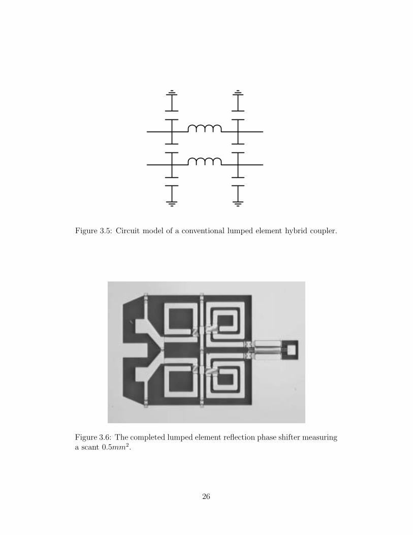
Figure 3.5: Circuit model of a conventional lumped element hybrid coupler.
Figure 3.6: The completed lumped element reflection phase shifter measuringa scant 0.5mm2.
26
0
50
100
150
200
9 9.5 10 10.5 11
0v
5v
10v
15v
20vS
21
(d
eg
)
Frequency (GHz)
Figure 3.7: The lumped element RTPS differential phase shift over frequency.
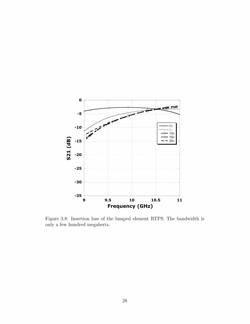
in figures 3.7 and 3.8. This 30/dB is a significant improvement over first
generation designs, and can be attributed to better modeling of the spiral
inductors.
3.4.3 Impedance transformed couplers
If the characteristic impedance presented to the reflective loads is reduced,
the achievable phase shift range can be increased. Since Z0 is a parameter
that impacts the entire system, it is necessary to use a transformer so that
only the reflective loads have to be altered. A quarter-wave transformer is
not a viable option for a compact circuit. If one was attached the lumped
coupler described previously, it would increase the size of the circuit by many
times. An lumped element LC transformer is a possibility, but would increase
27
-35
-30
-25
-20
-15
-10
-5
0
9 9.5 10 10.5 11
0v
5v
10v
15v
20v
S2
1 (
dB
)
Frequency (GHz)
Figure 3.8: Insertion loss of the lumped element RTPS. The bandwidth isonly a few hundred megahertz.
28
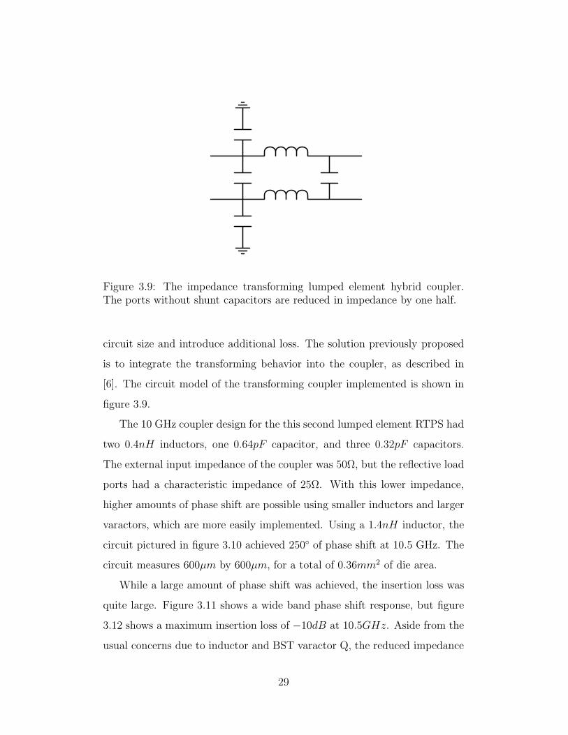
Figure 3.9: The impedance transforming lumped element hybrid coupler.The ports without shunt capacitors are reduced in impedance by one half.
circuit size and introduce additional loss. The solution previously proposed
is to integrate the transforming behavior into the coupler, as described in
[6]. The circuit model of the transforming coupler implemented is shown in
figure 3.9.
The 10 GHz coupler design for the this second lumped element RTPS had
two 0.4nH inductors, one 0.64pF capacitor, and three 0.32pF capacitors.
The external input impedance of the coupler was 50Ω, but the reflective load
ports had a characteristic impedance of 25Ω. With this lower impedance,
higher amounts of phase shift are possible using smaller inductors and larger
varactors, which are more easily implemented. Using a 1.4nH inductor, the
circuit pictured in figure 3.10 achieved 250 of phase shift at 10.5 GHz. The
circuit measures 600µm by 600µm, for a total of 0.36mm2 of die area.
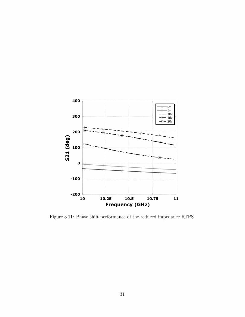
While a large amount of phase shift was achieved, the insertion loss was
quite large. Figure 3.11 shows a wide band phase shift response, but figure
3.12 shows a maximum insertion loss of −10dB at 10.5GHz. Aside from the
usual concerns due to inductor and BST varactor Q, the reduced impedance
29
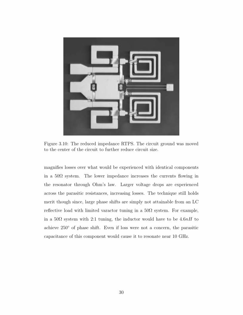
Figure 3.10: The reduced impedance RTPS. The circuit ground was movedto the center of the circuit to further reduce circuit size.
magnifies losses over what would be experienced with identical components
in a 50Ω system. The lower impedance increases the currents flowing in
the resonator through Ohm’s law. Larger voltage drops are experienced
across the parasitic resistances, increasing losses. The technique still holds
merit though since, large phase shifts are simply not attainable from an LC
reflective load with limited varactor tuning in a 50Ω system. For example,
in a 50Ω system with 2:1 tuning, the inductor would have to be 4.6nH to
achieve 250 of phase shift. Even if loss were not a concern, the parasitic
capacitance of this component would cause it to resonate near 10 GHz.
30
-200
-100
0
100
200
300
400
10 10.25 10.5 10.75 11
0v
5v
10v
15v
20v
S2
1 (
deg
)
Frequency (GHz)
Figure 3.11: Phase shift performance of the reduced impedance RTPS.
31
-35
-30
-25
-20
-15
-10
-5
0
10 10.25 10.5 10.75 11
0v
5v
10v
15v
20v
S2
1 (
mag
)
Frequency (GHz)
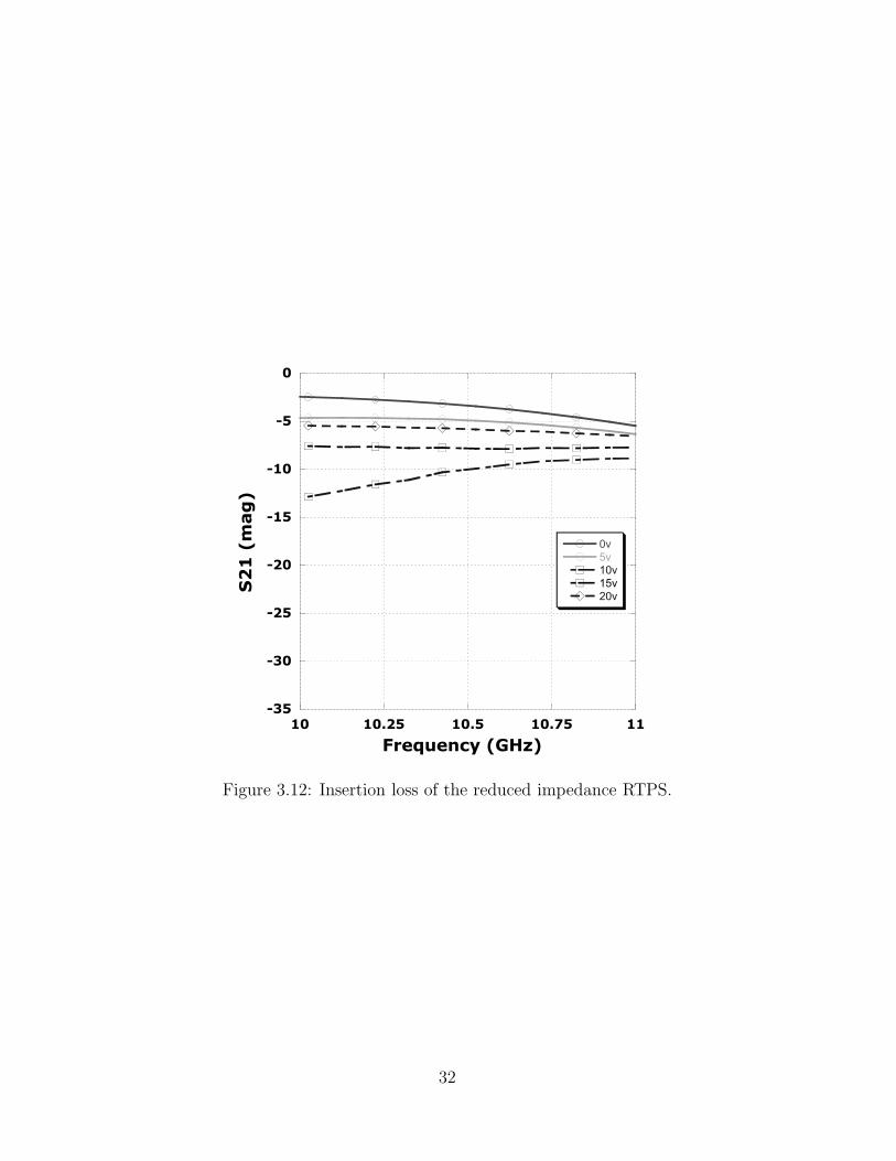
Figure 3.12: Insertion loss of the reduced impedance RTPS.
32
Bibliography
[1] T. Hirota, A. Minakawa, and M. Muraguchi, ”Reduced-Size Branch-line
and Rat-Race Hybrids for Uniplanar MMIC’s,” IEEE Trans. Microwave
Theory Tech., vol.38, no.3, pp. 270-275, March 1990
[2] F. Ellinger, R. Vogt, and W. Bachtold, ”Compact Reflective-Type Phase-
Shifter MMIC for C-Band Using a Lumped-Element Coupler,” IEEE
Trans. Microwave Theory Tech., vol.49, no.5, pp. 913-917, May 2001
[3] R.V. Garner, ”360 Varactor Linear Phase Modulator,” IEEE Trans. Mi-
crowave Theory Tech., vol. 17, no.3, pp. 137-147, March 1969
[4] D.M. Krafscik, S.A. Tmhoff, D.E. Dawson, and A.L. Conti, ”A Dual-
Varactor, Analog Phase Shifter Operating from 6 to 18 GHz,” IEEE
1988 Microwave and Millimeter-Wave Monolithic Circuits Symposium,
pp. 83-88
[5] D.M. Pozar, Microwave Engineering, Wiley, New York, 1998
[6] R.W. Vogel, ”Analysis and Design of Lumped and Lumped-Distributed
Element Directional Couplers for MIC and MMIC Applications,” IEEE
Trans. Microwave Theory Tech., vol.40, no.2, pp. 253-262, Feb. 1992
[7] J. Lange, ”Interdigitated Stripline Quadrature Coupler,” IEEE Trans.
Microwave Theory Tech., vol.17, pp. 1150-1151, Dec. 1969
33
Chapter 4
Distributed Analog PhaseShifters
The distributed analog phase shifter is attractive for its simple fabrication
and wide bandwidth. The device is realized by periodically loading a high
impedance transmission line with variable shunt capacitance. This results in
a transmission line with a tunable electrical length. There has been great
interest in the design recently, because of its compatibility with ferroelec-
tric and MEMS varactor technologies. The often understated drawback of
the distributed phase shifter is its long length. Devices operating around
10 GHz usually have lengths measured in centimeters. The low tuning ra-
tio of MEMS varactors results in a transmission line length several times
that of semiconductor or ferroelectric based designs. The long length makes
semiconductor based distributed phase shifters impractical for cost sensitive
applications. The lower fabrication costs of the alternative technologies make
the distributed phase shifter design more practical for low cost applications,
but reductions in length can further decrease costs and improve yields.
A distributed phase shifter is created by adding tunable capacitance to
a transmission line. Adjusting the capacitance alters the phase velocity of
the signal propagating along the line, varying its electrical length, and there-
fore the phase shift. Altering the capacitance also changes the characteristic
34
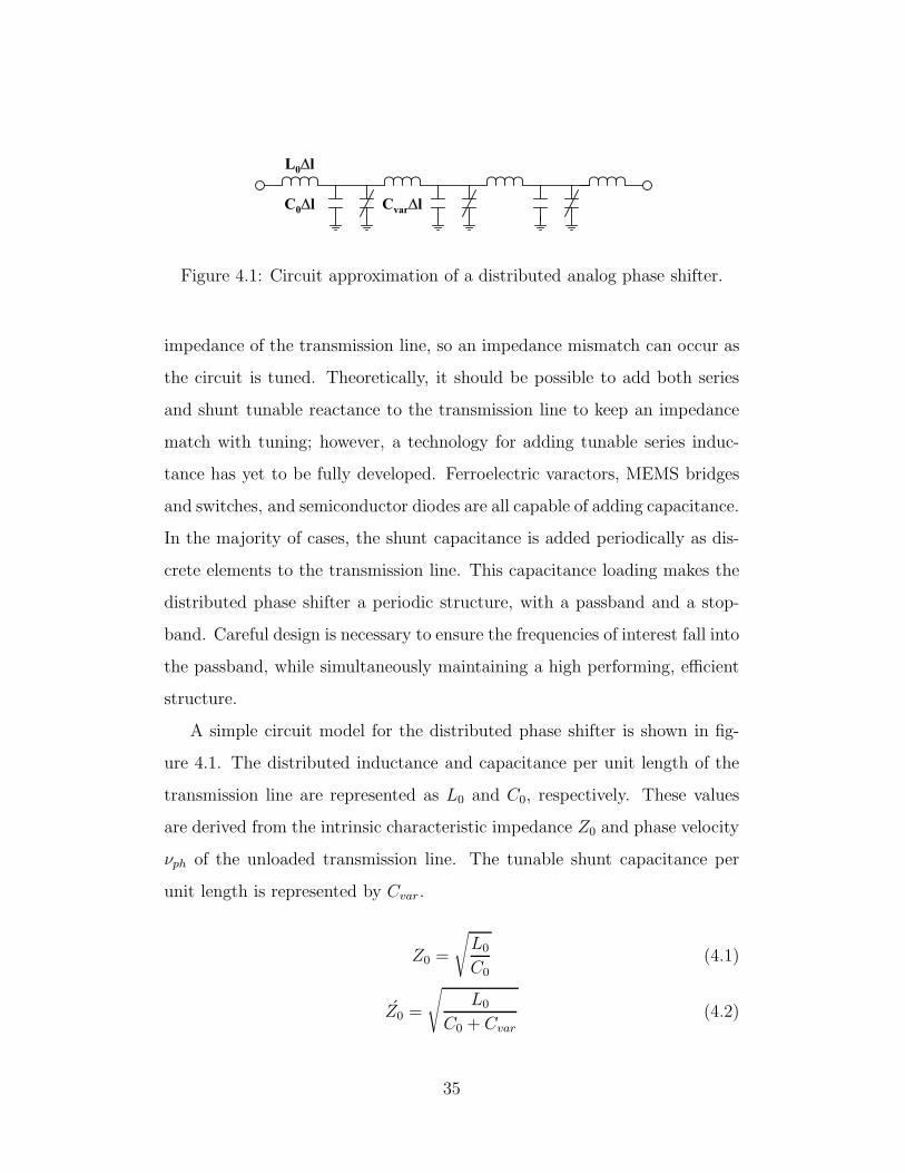
Cvar
lC0l
L0l
Figure 4.1: Circuit approximation of a distributed analog phase shifter.
impedance of the transmission line, so an impedance mismatch can occur as
the circuit is tuned. Theoretically, it should be possible to add both series
and shunt tunable reactance to the transmission line to keep an impedance
match with tuning; however, a technology for adding tunable series induc-
tance has yet to be fully developed. Ferroelectric varactors, MEMS bridges
and switches, and semiconductor diodes are all capable of adding capacitance.
In the majority of cases, the shunt capacitance is added periodically as dis-
crete elements to the transmission line. This capacitance loading makes the
distributed phase shifter a periodic structure, with a passband and a stop-
band. Careful design is necessary to ensure the frequencies of interest fall into
the passband, while simultaneously maintaining a high performing, efficient
structure.
A simple circuit model for the distributed phase shifter is shown in fig-
ure 4.1. The distributed inductance and capacitance per unit length of the
transmission line are represented as L0 and C0, respectively. These values
are derived from the intrinsic characteristic impedance Z0 and phase velocity
νph of the unloaded transmission line. The tunable shunt capacitance per
unit length is represented by Cvar.
Z0 =
√L0
C0(4.1)
Z0 =
√L0
C0 + Cvar
(4.2)
35
νph =1√
L0C0
(4.3)
νph =1√
L0(C0 + Cvar)(4.4)
The relationship between the distributed transmission line parameters
and the circuit model elements are given by equations (4.1) and (4.3). These
values are functions of the geometry and material properties of the trans-
mission line and cannot be changed. The addition of the tunable shunt
capacitance alters the effective characteristic impedance and phase velocity
as indicated in (4.2) and (4.4). It can be seen from equation (4.2) that the
addition of a Cvar lowers the characteristic impedance. Therefore it is nec-
essary that the intrinsic characteristic impedance of the transmission line be
larger than the characteristic impedance of the external circuit in order to
attempt an impedance match. A perfect match is not possible under all tun-
ing conditions, as can seen from equation (4.2), since Cvar varies with bias.
The variation of phase velocity, as in equation (4.4), is responsible for the
phase shifting behavior of the distributed phase shifter.
One crucial design aspect not covered by the previous equations is the
periodic nature of the circuit. The discontinuities created by the addition
of shunt elements results in small reflections from each element as the signal
propagates along the length of the circuit. As the frequency of the signal
approaches a certain value, the phases of the incident and reflected signal
interfere destructively, preventing forward propagation of the wave. When
the signal cannot propagate, the transmission loss increases, and the signal
is reflected back towards the source. The frequency where the signal is com-
pletely prevented from forward propagation is called the Bragg frequency,
after a similar phenomenon in crystalline solids. The relationship between
this frequency, fBragg and the circuit model elements is defined in equation
(4.5).
36
fBragg =1
π∆l√
L0(C0 + Cvar)(4.5)
The ∆l parameter represents the spacing between tuning capacitors, and
can be adjusted to change the Bragg frequency independent of the other
transmission line parameters. The highest operating frequency of the phase
shifter must be significantly below fBragg to avoid large transmission losses.
Modeling the circuit with ABCD matrices will easily demonstrate how trans-
mission loss varies with fBragg. The phase shift of each section of the dis-
tributed phase shifter varies as νph is tuned. The length ∆l divided by the
change in νph determines the differential phase shift of the section. This is
expressed in equation (4.6) with the phase velocity expanded into its con-
stituent terms. The terms Cmin and Cmax denote the extremes of the values
Cvar can assume with tuning. A sufficient number of sections should be
cascaded to obtain the desired differential phase shift.
∆φ = 360f∆l√
L0(√
C0 + Cmax −√
C0 + Cmin) (4.6)
A loss optimized distributed phase shifter design depends on proper se-
lection of ∆l and Z0. Increasing ∆l brings the Bragg frequency closer to the
operating frequency and reduces the number of sections required to achieve
a desired phase shift. Increasing Z0 lowers C0 and allows a greater vari-
ation in νph, and also reducing the number of sections. This is beneficial
if the tunable capacitor is lossy, since fewer are needed in a given design.
However, operating closer to the Bragg frequency increases the transmission
loss through reflection of the input signal. Also, high impedance transmission
lines generally have higher loss than lower impedance ones. These conflicting
requirements lead to an optimized design that balances the sources of loss,
resulting in the lowest loss design. As a result, the best design from a loss
37
perspective may not necessary have the shortest length or fewest sections.
4.1 Strategies for Size Reduction
As mentioned previously, the principal drawback of the distributed analog
phase shifter is its long length. If the number of sections can be decreased or
if the individual sections are shortened while maintaining the desired phase
shift, the overall phase shifter length can be reduced. Both of these ob-
jectives can be achieved by increasing the characteristic impedance of the
unloaded transmission line. Increasing Z0 decreases the distributed capaci-
tance, allowing a larger loading capacitor. The increase in loading capacitor
to distributed capacitance ratio increases the phase shift per section. Also,
increasing Z0 increases the distributed inductance, leading to a shorter sec-
tion length for a given fBragg.
Coplanar waveguide has been the favored transmission line medium to
date for the implementation of distributed phase shifter circuits. The simple
connection of shunt elements makes it ideal for connecting a large number of
varactors to ground. This is true regardless of the technology used; semicon-
ductor diodes, microelectromechanical membranes, and ferroelectric thin film
varactors are all easily integrated into the coplanar waveguide transmission
line structure.
Normal use of CPW in MMICs as an interconnect or resonant element
requires it to have a characteristic impedance of 50 Ohms. For most sub-
strate materials, this is close to lowest attenuation impedance. When the
impedance increases much above this value, the center conductor width nar-
rows rapidly, and high transmission losses are incurred. In [1], an optimiza-
tion procedure was developed to balance this transmission line loss against
the increased varactor diode loss encountered with using lower impedance
lines. In [2], quartz substrate material with a dielectric constant of 4 was
38
used make lower loss high impedance CPW transmission lines. The low di-
electric constant widens the center conductor considerably. However, this
strategy renders the standard 50Ω line rather lossy for reasonable ground
to ground separations, making it a poor choice for integration with other
distributed circuit elements. Also, the effective relative dielectric constant
of the transmission line decreases to less than 3, further increasing the dis-
tributed phase shifter length. In [3], a moderately high transmission line
impedance of 70Ω was used, but the ground to ground spacing of the CPW
line was increased considerably to widen the center conductor width. The
transmission line loss was kept low, but at a considerable expense in chip
area. A cross section of the tranmission line used there measures nearly half
a centimeter in width, enormous by integrated circuit standards.
Two different strategies were pursued here to realize reduced size dis-
tributed analog phase shifters. One method is to do away with the transmis-
sion line, and implement the inductance with a planar spiral inductor. This
technique shrinks each unit cell considerably, but is limited in frequency. The
other technique is to utilize the coplanar strip transmission line. This little
used transmission line has low loss high impedance lines, making it ideally
suited for distributed phase shifters. Both methods present additional chal-
lenges and drawbacks, but both are more viable for mass production than
the avenues pursued previously.
4.2 Synthetic Transmission Lines
The distributed analog phase shifter is amenable to implementation with the
transmission line replaced by a planar spiral inductor. While elimination of
the distributed transmission line may make the name seem inappropriate,
the principle is the same. Each unit cell of the lumped analog phase shifter
consists of a spiral inductor and a shunt varactor. The fixed capacitor to
39
ground in figure 4.1 is eliminated, except as a parasitic. The structure re-
tains the same wideband frequency characteristics of the distributed version,
but is considerably smaller. At frequencies around or below 5 GHz, where
distributed elements are unthinkable due to size constraints, the use of spiral
inductors makes the distributed analog phase shifter a viable option.
The well known difficulties in closed form modeling of spiral inductors is
not as serious a drawback here as in other designs. Since the phase shifter
consists of a unit cell repeated many times, only one inductance value is
needed. The principal drawback of using spiral inductors is their increased
loss compared to transmission lines. Optimization with electromagnetic field
solvers can be carried out to find the inductor geometry with the lowest series
resistance.
An additional optimization parameter is available here that is not directly
applicable in a truly distributed structure. It was previously stated that
fBragg should be set to a frequency sufficiently above the operating frequency
to reduce return losses. This frequency must also be kept sufficently close
to the operating frequency to keep the number of sections to a minimum.
The total length of the transmission line is identical regardless of the Bragg
frequency, making the line attenuation a constant. In most technologies,
it is desirable to keep the number of sections low to reduce the cumulative
varactor loss.1 When spiral inductors are used instead of transmission lines,
the assumption of constant line loss regardless of Bragg frequency is no longer
true. A lower fBragg design using a smaller number of higher valued inductors
may incur more loss than a design using a larger number of smaller inductors.
The variation of inductor Q with inductance is complicated, and must be
found through electromagnetic simulation. Additional complications result
1While the individual varactor values vary with changes in the Bragg frequency, it isassumed here that the fixed loss of a varactor is much greater than the value dependentloss variation.
40
Figure 4.2: An X-band quasi-distributed analog phase shifter.
when inductor Q and varactor Q are similar in magnitude, leading to a
complex relationship for the lowest loss design.
As with the previous phase shifter designs presented, the design frequency
for this work was 10 GHz. The X-band frequency range, in addition to
being of interest for phased array radars, is sufficiently high that distributed
techniques are compact enough to be considered for use. This frequency
range also begins to test the limits of spiral inductor usage, mainly due to
loss considerations, but due to parasitic capacitance and self-resonance.
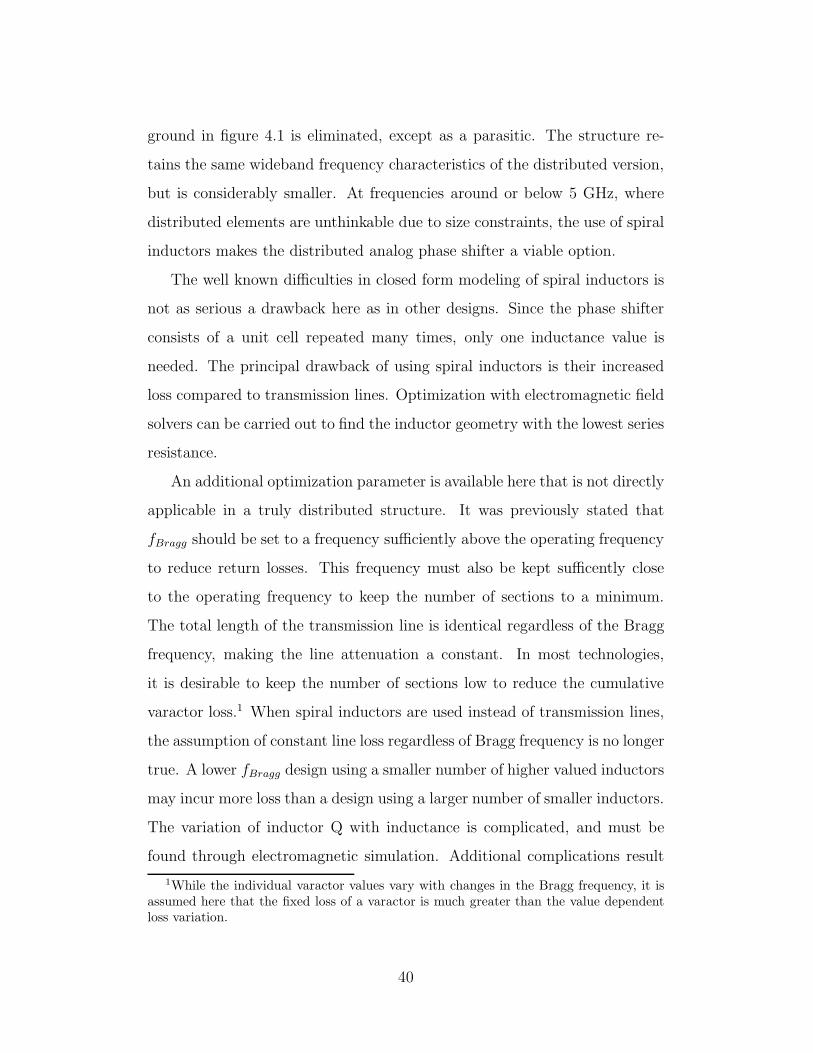
A synthetic transmission line phase shifter is pictured in 4.2. The three
section device was designed to provide 90 of phase shift at 10 GHz. It mea-
sured 1.5mm in length, with a total area of 0.75mm2. A difference from
an earlier device presented in [4] is the removal of the coplanar waveguide
launch. In that structure, two varactors were connected in parallel at each
inductor node to maintain symmetry. Theoretically, this should half the
parasitic varactor resistance and increase Q. Due to the asymmetry in the
inductor causing uneven ground voltages, and the extremely small electrode
areas, it was believed that a single varactor design would be higher perform-
ing. The inductors were 0.8 nH and the maximum varactor capacitance was
0.5 pF. Without any distributed transmission line capacitance, the tuning of
the varactors for phase shift greatly impacts the characteristic impedance of
41
the device. At zero bias, the structure was designed to have a Z0 of 63Ω,
reducing to 47Ω under tuning.
Each inductor consisted of 1.5 turns of 43µm wide traces, with a turn
spacing of 23µm and an outer diameter of 380µm. The circular topology
theoretically has higher Q, but later designs switched to square spirals to
reduce EM simulation times. To increase the metal thickness, the air-bridge
layer metalization was overlaid partially onto the spiral trace, giving a 2µm
layer of gold. Assuming a conductivity of 2 ∗ 107S/m, EM simulation indi-
cated a Q of 50.
The varactors were implemented using the BST parallel plate capacitor
process. The top plate measured 5.8µm by 5.8µm, with a ground spacing of
2µm. This was an early design, so it did not take into account the consider-
able fringing capacitance of the top electrode. The low frequency capacitor Q
was approximately 50. While the design assumed a 3:1 capacitance change,
only approximately 2:1 was achieved. This limited the maximum phase shift
attainable with the device.
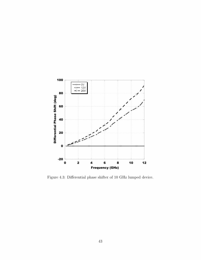
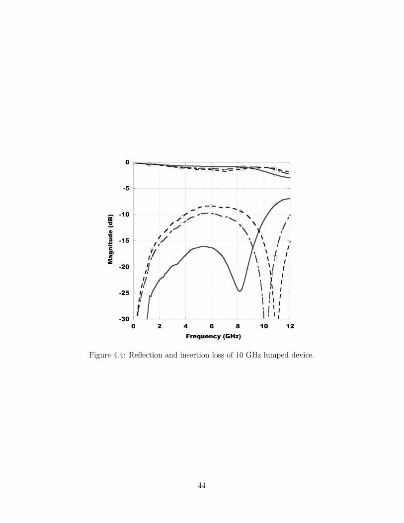
The phase shifter managed to achieve 72 differential phase shift with
−1.7dB insertion loss at the design frequency of 10 GHz. This resulted in a
figure of merit of 42/dB. Return loss was kept below −10dB. The actual
test data are summarized in figures 4.3 and 4.4. This performance is very
promising, due to the extremely compact circuit size. A complete 360 design
should be achievable in less than 3.0mm2 of die area, making it extremely cost
competitive to commercial MMIC designs. To make the device performance
competitive, the figure of merit should improve to at least 90/dB. To achieve
this, higher component Qs are necessary. The inductor Q of 50 is quite good,
but could be improved upon by copper or silver metalization. The main
obstacle at present is the BST varactor loss. Both electrode loss and film
loss are significant contributors. Thin, resistive electrode layers are the result
42
-20
0
20
40
60
80
100
0 2 4 6 8 10 12
0V
12V
20V
Dif
fere
nti
al
Ph
ase
Sh
ift
(de
g)
Frequency (GHz)
Figure 4.3: Differential phase shifter of 10 GHz lumped device.
43
-30
-25
-20
-15
-10
-5
0
0 2 4 6 8 10 12
Ma
gn
itu
de
(d
B)
Frequency (GHz)
Figure 4.4: Reflection and insertion loss of 10 GHz lumped device.
44
of high BST growth temperatures and the limitations of contact lithography.
Film loss is worsened by long growth times (approximately 3 hours) necessary
to increase electrode areas. Most of these issues can be rectified with better
process technology.
Attempts were made to improve upon these results with another design
iteration. Three devices were designed to provide 180 differential phase
shift. These devices varied in mainly in the choice of inductor geometry.
However, time constraints only permitted one successful process run. The
device figure of merits did not exceed those previously presented. While
these designs used square spiral inductors, it is believed the fault lay mainly
in poor BST varactor performance.
4.3 High Impedance Coplanar Strip Trans-
mission Lines
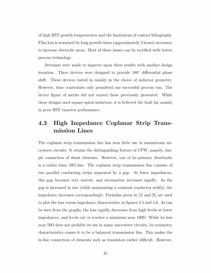
The coplanar strip transmission line has seen little use in mainstream mi-
crowave circuits. It retains the distinguishing feature of CPW, namely, sim-
ple connection of shunt elements. However, one of its primary drawbacks
is a rather lossy 50Ω line. The coplanar strip transmission line consists of
two parallel conducting strips separated by a gap. At lower impedances,
this gap becomes very narrow, and attenuation increases rapidly. As the
gap is increased in size (while maintaining a constant conductor width), the
impedance increases correspondingly. Formulas given in [5] and [6] are used
to plot the loss versus impedance characteristic in figures 4.5 and 4.6. As can
be seen from the graphs, the loss rapidly decreases from high levels at lower
impedances, and levels out or reaches a minimum near 100Ω. While its loss
near 50Ω does not prohibit its use in many microwave circuits, its symmetry
characteristics causes it to be a balanced transmission line. This makes the
in-line connection of elements such as transistors rather difficult. However,
45
50 75 100 125 150 175 200Z0 HΩL
1
2
3
4
5αc HdBêcmL
Figure 4.5: Loss versus characteristic impedance plotted with a constantconductor width of 50µm. The substrate has a relative dielectric constant of10.2, and the metalization is 1µm of gold.
CPS can easily be integrated with CPW, as demonstrated in [7]. With this
in mind, the balanced nature of CPS circuit components can exploited to
effect in carefully designed microwave integrated circuits.
At very high impedances the distributed capacitance of a transmission
line becomes almost negligible in comparison to the loading capacitance nec-
essary to reduce its impedance to 50Ω. This makes sections of coplanar strip
comprising a distributed phase shifter almost entirely inductive. Unlike a
spiral inductor, the coplanar strip segment doesn’t have a maximum useful
frequency determined by its self-resonant frequency. A distributed transmis-
sion line phase shifter can be designed for frequencies much beyond those
achievable by synthetic line phase shifters. At frequencies where spiral in-
ductors are still useful, coplanar strip designs can still be used where loss
performance is critical, and die area is not as much of a concern. CPS based
distributed phase shifters at any frequency are still much more cost-effective
than CPW based designs.
Unlike CPW, which becomes lossy at both low and high impedances,
CPS’s loss continually decreases almost continually with increasing impedance.
46
50 75 100 125 150 175 200Z0 HΩL
1
2
3
4
5αc HdBêcmL
Figure 4.6: Loss versus characteristic impedance plotted while holding theoverall transmission line width constant at 200µm, and varying the conductorwidth and spacing. The material parameters are as before.
The limitation on how high of an impedance can be used is usually based
on geometry considerations. As the impedance is raised, the gap between
the conductors increases steadily, if the conductor widths are held constant.
Eventually, the gap will become comparable in value to the substrate thick-
ness. When this occurs, it will become possible to excite the parasitic
microstrip mode at discontinuities. It may also become difficult to excite
the line. The CPS gap must therefore be kept below the substrate thick-
ness. Shrinking the conductor widths will decrease the gap size for a given
impedance, but will also increase loss.
Another concern with high impedance levels in CPS occurs at high fre-
quencies. The conductor width and gap combination chosen for low loss per-
formance may become comparable to the section length at higher microwave
frequencies. This is not recommended because the parasitic inductance of
the shunt connection between the two conductors becomes significant com-
pared to the distributed inductance and varactor capacitance of each section.
It therefore becomes necessary to shrink the conductor and gap dimensions,
increasing transmission line loss.
47
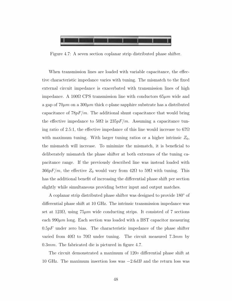
Figure 4.7: A seven section coplanar strip distributed phase shifter.
When transmission lines are loaded with variable capacitance, the effec-
tive characteristic impedance varies with tuning. The mismatch to the fixed
external circuit impedance is exacerbated with transmission lines of high
impedance. A 100Ω CPS transmission line with conductors 65µm wide and
a gap of 70µm on a 300µm thick c-plane sapphire substrate has a distributed
capacitance of 78pF/m. The additional shunt capacitance that would bring
the effective impedance to 50Ω is 235pF/m. Assuming a capacitance tun-
ing ratio of 2.5:1, the effective impedance of this line would increase to 67Ω
with maximum tuning. With larger tuning ratios or a higher intrinsic Z0,
the mismatch will increase. To minimize the mismatch, it is beneficial to
deliberately mismatch the phase shifter at both extremes of the tuning ca-
pacitance range. If the previously described line was instead loaded with
366pF/m, the effective Z0 would vary from 42Ω to 59Ω with tuning. This
has the additional benefit of increasing the differential phase shift per section
slightly while simultaneous providing better input and output matches.
A coplanar strip distributed phase shifter was designed to provide 180 of
differential phase shift at 10 GHz. The intrinsic transmission impedance was
set at 123Ω, using 75µm wide conducting strips. It consisted of 7 sections
each 990µm long. Each section was loaded with a BST capacitor measuring
0.5pF under zero bias. The characteristic impedance of the phase shifter
varied from 40Ω to 70Ω under tuning. The circuit measured 7.3mm by
0.3mm. The fabricated die is pictured in figure 4.7.
The circuit demonstrated a maximum of 120 differential phase shift at
10 GHz. The maximum insertion loss was −2.6dB and the return loss was
48
-50
0
50
100
150
200
0 2 4 6 8 10 12
0V
12V
20V
Dif
fere
nti
al
Ph
ase
Sh
ift
(de
g)
Frequency (GHz)
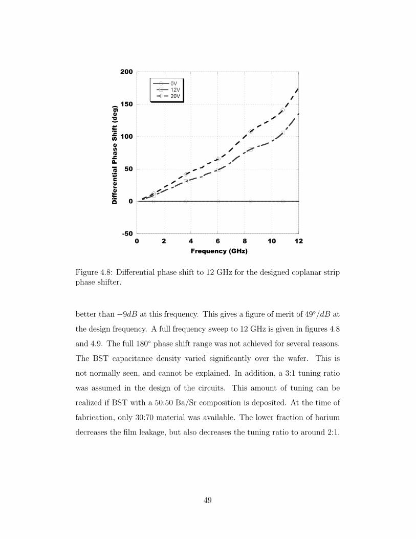
Figure 4.8: Differential phase shift to 12 GHz for the designed coplanar stripphase shifter.
better than −9dB at this frequency. This gives a figure of merit of 49/dB at
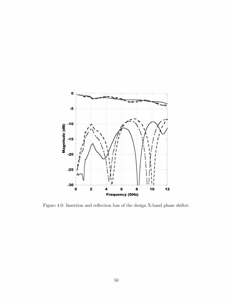
the design frequency. A full frequency sweep to 12 GHz is given in figures 4.8
and 4.9. The full 180 phase shift range was not achieved for several reasons.
The BST capacitance density varied significantly over the wafer. This is
not normally seen, and cannot be explained. In addition, a 3:1 tuning ratio
was assumed in the design of the circuits. This amount of tuning can be
realized if BST with a 50:50 Ba/Sr composition is deposited. At the time of
fabrication, only 30:70 material was available. The lower fraction of barium
decreases the film leakage, but also decreases the tuning ratio to around 2:1.
49
-30
-25
-20
-15
-10
-5
0
0 2 4 6 8 10 12
Magnit
ude (
dB
)
Frequency (GHz)
Figure 4.9: Insertion and reflection loss of the design X-band phase shifter.
50
4.4 Comparisons
The relative dimensions of the two circuits can be compared. If the lumped
element design is scaled to a 180, it will measure 3.0mm. This is less than
half the length of the 7.3mm CPS phase shifter. The area consumed by
the lumped circuit is a fraction of that occupied by the CPS circuit, which
requires a ’buffer’ between adjacent lines to mitigate coupling effects. The
lumped circuit is not as sensitive to coupling effects. The figure of merit of the
lumped version is competitive with the CPS circuit, 42/dB versus 49/dB.
It is not expected that this trend would continue for higher frequencies. The
loss in high frequency spiral inductors is expected to make such lumped phase
shifters unfeasible at or above K-band. Data from a CPW distributed phase
shifter described in [3] indicates a figure of merit of 80/dB. The CPW based
circuit offers with best performance in term of loss, but its area is much larger
than the other circuits. Measuring 17.5 mm by 3.5 mm, its dimensions ensure
wide conductors and a low loss transmission line. It is very inefficient from an
area perspective, consuming over half a square centimeter of substrate area.
The CPS based circuit consumes only a sixth of the area, but offers superior
performance in terms of loss per unit length. The degrees per decibel figure
of merit can clearly stand some improvement to make it more comparable to
the CPW version. The lumped circuit consumes only one thirtieth the area
of the CPW circuit, but still manages to attain reasonable loss performance.
Clearly, when the operating frequencies are low enough, lumped transmis-
sion line phase shifters are superior from a cost perspective. The reduced size
also offers benefits from an integration standpoint. From the perspective of
ultimate loss performance regardless of chip area, the CPW design is still ad-
vantageous. Although it not complete obvious from the set of data presented
here, we believe the CPS distributed phase shifter has advantages over both
51
designs. It is possible to scale the CPS circuit to frequencies beyond those
feasible with lumped elements, while maintaining a size advantage over CPW
circuits. The results are still encouraging. A new type of distributed phase
shifter using the coplanar strip transmission line topology was presented that
achieved a 49/dB figure of merit. A lumped transmission line circuit was
also presented that achieved a 42/dB figure of merit. Both circuits utilized
thin film ferroelectric technology and operated at 10 GHz.
52
Bibliography
[1] A.S. Nagra and R.A. York, ”Distributed Analog Phase Shifters with Low
Insertion Loss, ” IEEE Trans. Microwave Theory Tech., vol.47, no.9, pp.
1705-1711, Sept. 1999
[2] N.S. Barker and G.M. Rebeiz, ”Optimization of Distributed MEMS
Transmission-Line Phase Shifters – U-Band and W-Band Designs,” IEEE
Trans. Microwave Theory Tech., vol.48, no.11, pp. 1957-1966, Nov. 2000
[3] B. Acikel, T. R. Taylor, P. J. Hansen, J. S. Speck, and R. A. York, ”A
New High Performance Phase Shifter using BaSrTiO3 Thin Films,” IEEE
Microwave and Wireless Component Letters, vol.12, no.7, pp. 237-239,
July 2002.
[4] J. Serraiocco, B. Acikel, P. Hansen, T. Taylor, H. Xu, J.S. Speck, and
R.A. York, ”Tunable Passive Integrated Circuits using BST Thin Films,”
Proceedings of the International Symposium on Integrated Ferroelectrics,
Nara, Japan, June 2002
[5] E. Chen and S.Y. Chou, ”Characteristics of Coplanar Transmission Lines
on Multilayer Substrates: Modeling and Experiments,” IEEE MTT June
1997
[6] G. Ghione, ”A CAD-Oriented Analytical Model for the Losses of Gen-
eral Asymmetric Coplanar Lines in Hybrid and Monolithic MICs,” IEEE
MTT Sept. 1993
53

[7] M.C. Scardelletti, G.E. Ponchak, and T.M. Weller, ”Miniaturized Wilkin-
son Power Dividers Utilizing Capacitive Loading,” IEEE Microwave and
Wireless Components Letters, vol.12, no.1, pp. 6-8, Jan. 2002
54
Chapter 5
Conclusion
A number of compact phase shifters using the integrated BST varactor pas-
sives process have been presented. The circuits fall into two categories, with
either size or performance as their emphasis. The RTPS is a simple design
advantageous when smaller amounts of phase shift are needed, while the
distributed phase shifter can be scaled up to arbitrarily large phase shifts.
These designs can be implemented in almost any technology, but the inte-
grated BST process can potentially be made much cheaper.
Reflection type phase shifters implemented using lumped components
have a clear advantage over other designs in terms of die size. An X-band de-
sign presented here measured a miniscule 0.36mm2 in size. To obtain equally
impressive loss performance requires careful design entailing extensive elec-
tromagnetic simulation, and high quality lumped components. While MIM
capacitors and BST varactors can be scaled up in frequency beyond 20 GHz,
spiral inductors cannot. This is not a serious hindrance; distributed com-
ponents can easily be substituted at these frequencies. The RTPS design is
however more difficult to scale to large phase shifts than other designs. The
tunability ratio places a restriction on the amount of attainable phase shift.
This can be extended at lower frequencies by using an integral impedance
transformer, which maintains compact circuit size. The design mentioned
55
previously attained 250 of phase shift with −10dB insertion loss. 25/dB
is clearly not competitive enough for commercial use, but with further opti-
mization and improvements in the BST varactor Q, higher figures of merit
are possible.
Distributed analog phase shifters have already proven themselves with
regard to loss and frequency scalability. Current implementations are ex-
cessively large, due to the large number of sections required to achieve the
designed phase shift. By transitioning to a coplanar strip transmission line,
distributed phase shifters can be realized with higher intrinsic characteristic
impedances. This allows heavier loading of the transmission line, resulting
in shorter sections with greater amounts of phase shift. This translates into
a shorter overall design, consuming less die area, and requiring fewer varac-
tors. A X-band coplanar strip distributed analog phase shifter presented here
attained 120 of phase shift while measuring 7.2mm in length. An attempt
was made to further shrink this design by using spiral inductors instead of a
transmission line. One design achieved 42/dB figure of merit. When scaled
this design would be less than half the length of the CPS version, while
maintaining competitive performance. This technique can be used to extend
the performance and true time delay characteristics of the distributed phase
shifter to low microwave frequencies.
56