high-speed type-ii gaassb/inp dhbts for mixed-signal ic
TRANSCRIPT
HIGH-SPEED TYPE-II GaAsSb/InP DHBTs FOR MIXED-SIGNAL IC APPLICATIONS
BY
HUIMING XU
DISSERTATION
Submitted in partial fulfillment of the requirements
for the degree of Doctor of Philosophy in Electrical and Computer Engineering
in the Graduate College of the
University of Illinois at Urbana-Champaign, 2014
Urbana, Illinois
Doctoral Committee:
Professor Milton Feng, Chair
Associate Professor John Dallesasse
Professor Jianming Jin
Associate Professor Xiuling Li
ii
ABSTRACT
Heterojunction bipolar transistors (HBTs) are widely used in high-speed mixed-signal, radio
frequency, and communication ICs because of their high speed, high breakdown voltage, and high
efficiency capabilities compared with Si bipolar junction transistors (BJTs) and complementary
metal-oxide semiconductor (CMOS) transistors. Among different HBTs, InP HBTs offer the
highest frequency operation capability with reasonably high breakdown voltage. Thus, InP HBTs
are becoming increasingly important for high-speed mixed-signal ICs. Depending on different
heterojunction band alignments, there are mainly three types of InP HBTs, namely, InGaAs/InP
single heterojunction bipolar transistor (SHBT), Type-I InGaAs/InP double heterojunction bipolar
transistor (DHBT), and Type-II GaAsSb/InP DHBT. Among these three types of InP HBTs, Type-
II GaAsSb/InP DHBT has the most favorable band alignment; thus it has many superiorities
compared with other InP HBT technologies.
The subject of this work is the design, fabrication, and characterization of Type-II GaAsSb/InP
HBTs. Chapter 1 of this work gives an overview of the development of InP HBTs and relevant
figures of merit for HBTs. It will also give an introduction of different Types of InP HBTs. In
Chapter 2, InP HBT material structure design, device fabrication process, and scaling are
discussed. In Chapter 3, the DC, RF, and nonlinearity characterization of a Type-I/II
AlInP/GaAsSb/InP DHBT will be performed and compared to that of a Type-I InP/InGaAs/InP
DHBT. The physical origins of nonlinearity in Type-I InP/InGaAs/InP DHBT will also be
discussed in Chapter 3. Chapter 4 details the design and performance of a composition-graded
AlGaAsSb base Type-II InP DHBT. Small-signal modelling and time delay analysis show that a
composition-graded AlGaAsSb base can greatly reduce the base transit time and improve device
RF performance. Chapter 5 details the design and performance of a doping-graded GaAsSb base
iii
Type-II GaAsSb/InP DHBT. Small-signal modelling and time delay analysis show that a doping-
graded GaAsSb base can result in base transit time comparable with a composition-graded
AlGaAsSb base. It is also shown that as device emitter width scales down, the emitter peripheral
surface recombination current becomes a significant portion of the total base current, leading to
reduced current gain. Chapter 6 discusses the development of an emitter ledge process for the
doping-graded Type-II GaAsSb/InP DHBT. Compared with devices without an emitter ledge,
devices with an AlInP emitter ledge have shown much lower emitter peripheral surface
recombination current density. Thus, the AlInP emitter ledge can effectively suppress the emitter
size effect and improve current gain. Chapter 7 gives a brief summary of this work.

iv
To my family

v
ACKNOWLEDGMENTS
I would like to thank my adviser, Professor Milton Feng, for the opportunity to become a
member of his research group and for his continuous support and guidance throughout my graduate
studies. It has been a great privilege to work in a research group as accomplished as the High-
Speed Integrated Circuits (HSIC) Group.
I am grateful for the mentoring of Professor Feng’s former student Dr. K. Y. (Donald) Cheng,
who taught me the double heterojunction bipolar transistor (DHBT) processing techniques step by
step, and Dr. Doris Chan, who taught me monolithic microwave integrated circuit (MMIC) design
and radio frequency (RF) measurement techniques. I also benefited greatly from the material
growth expertise of Professor Keh-Yung Cheng and the hard work of his former and current
students, Dr. Bing-Ruey (Barry) Wu and Chi-chih (Keith) Liao, without whom this work would
not have been possible. Credit also goes to former students Dr. Michael Hattendorf, Dr. Walid
Hafez, and Dr. Will Snodgrass for laying the foundations of the HSIC group sub-micron transistor
work. I am also thankful for current and former HSIC group members Dr. Mark Stuenkel, Dr.
Chao-Hsin (Wayne) Wu, Dr. Fei Tan, Dr. Mong-kai Wu, Eric Iverson, Rohan Bambery, Michael
Liu, Curtis Wang, and Ardy Winoto. I have relied heavily on their support and collective
knowledge of semiconductor device fabrication and characterization.
I thank my family for their encouragement throughout the years. Their patience and support
are the foundation of everything I have achieved.
vi
TABLE OF CONTENTS
1 INTRODUCTION…………………………………………………………………………..... 1
1.1 Development of InP Heterojunction Bipolar Transistors………...…….………… 1
1.2 High-Frequency Transistor Figures of Merit……….………………………….…. 2
1.3 Different Types of HBTs…………………………..………………………….….. 4
1.4 Summary of Different InP HBT Technologies……………………………………. 8
2 TYPE-II InP DHBT DESIGN AND FABRICATION……….……………..……………….. 9
2.1 InP and Related Materials………………………………………………………… 9
2.2 Type-II InP DHBT Layer Structure Design………………………………….…… 11
2.3 Sub-Micron DHBT Fabrication Process…………………………….……………. 15
2.4 Scaling of Sub-Micron DHBT ……………………………………………….….... 17
3 CHARACTERIZATION AND COMPARISON OF TYPE-I AND TYPE-I/II InP DHBTs… 19
3.1 DC Characterization of InP DHBTs….…………….…………………………….. 19
3.2 RF Characterization of InP DHBTs...…………………………………………….. 21
3.3 Nonlinearity Characterization of InP DHBTs…………………………………….. 23
3.4 Physical Origins of Nonlinearity………………………………………………….. 24
4 COMPOSITION-GRADED AlGaAsSb BASE TYPE-II InP DHBT………………………… 27
4.1 Composition-Graded AlGaAsSb Base Type-II InP DHBT Layer Structure……… 27
4.2 DC and RF Performance of Graded AlGaAsSb Base Type-II InP DHBT…...…… 29
4.3 Small-Signal Modeling and Parameter Extraction of Type-II InP DHBT……...… 32
4.4 Graded AlGaAsSb Base Type-II InP DHBT Transit Time Analysis……..………. 38
vii
5 DOPING-GRADED BASE TYPE-II GaAsSb/InP DHBT........................................................ 40
5.1 Doping-Graded Base Type-II GaAsSb/InP DHBT……………………………….. 40
5.2 DC and RF Performance of Doping-Graded Base Type-II GaAsSb/InP DHBT…..42
5.3 Emitter Size Effect of Type-II GaAsSb/InP DHBT…………………...……..…… 46
6 DOPING-GRADED BASE TYPE-II GaAsSb/InP DHBT WITH AN EMITTER LEDGE…. 50
6.1 Emitter Ledge Process Development…………………………………………..….. 50
6.2 DC and RF Performance of Type-II GaAsSb/InP DHBT with an Emitter Ledge....51
6.3 Emitter Size Effect of Type-II GaAsSb/InP DHBT with an Emitter Ledge…….....55
7 CONCLUSION ………………..…..….…………………………………………………..…... 57
REFERENCES……………………………………………………..………………………........ 59
1
1 INTRODUCTION
1.1 Development of InP Heterojunction Bipolar Transistors
After the invention of the point contact transistor by Bardeen and Brattain in 1947 [1], Shockley
developed the theory of minority carrier injection in 1949 [2], and subsequently demonstrated the
first bipolar junction transistor (BJT) in 1951 [3]. In a 1948 patent application, Shockley proposed
the idea of using a material having a wider energy band gap for the emitter of a BJT to increase
the minority carrier injection efficiency [4]. Kroemer developed the idea of using wider energy
band gap material for the emitter of a BJT and proposed the first heterojunction bipolar transistor
(HBT) structure in 1957 [5]. In contrast to BJT, HBT has a wider band gap emitter, which can
prevent hole injection into the emitter from the base under forward bias conditions. Thus, the base
of a HBT could be heavily doped while maintaining high current gain. Moreover, because of the
heavy doping, the base could be made very thin without introducing large base sheet resistance.
So, the transit time through the base could be reduced and speed of the transistor could be improved.
As with any other heterostructure devices, the HBT technology has been progressing rapidly after
the material growth technologies were matured. Nowadays, InGaP/GaAs HBTs are widely used
for high-efficiency RF power amplifiers in wireless devices. Compared with GaAs HBTs, InP
HBTs have lower turn-on voltage because of the narrower base energy band gap. In addition, InP
has superior transport properties than do GaAs; thus InP HBTs can achieve a very high amplifier
gain-bandwidth product per DC power ratio (GBP/PDC) for low supply voltage [6]. InP-based
HBTs are well suited for the high-speed mixed-signal ICs in high data rate optical communication
systems and high-speed testing instrumentations [7, 8].
2
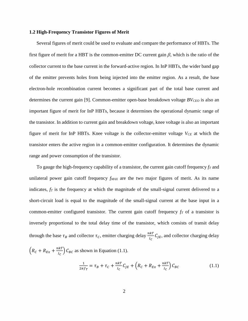
1.2 High-Frequency Transistor Figures of Merit
Several figures of merit could be used to evaluate and compare the performance of HBTs. The
first figure of merit for a HBT is the common-emitter DC current gain , which is the ratio of the
collector current to the base current in the forward-active region. In InP HBTs, the wider band gap
of the emitter prevents holes from being injected into the emitter region. As a result, the base
electron-hole recombination current becomes a significant part of the total base current and
determines the current gain [9]. Common-emitter open-base breakdown voltage BVCEO is also an
important figure of merit for InP HBTs, because it determines the operational dynamic range of
the transistor. In addition to current gain and breakdown voltage, knee voltage is also an important
figure of merit for InP HBTs. Knee voltage is the collector-emitter voltage VCE at which the
transistor enters the active region in a common-emitter configuration. It determines the dynamic
range and power consumption of the transistor.
To gauge the high-frequency capability of a transistor, the current gain cutoff frequency fT and
unilateral power gain cutoff frequency fMAX are the two major figures of merit. As its name
indicates, fT is the frequency at which the magnitude of the small-signal current delivered to a
short-circuit load is equal to the magnitude of the small-signal current at the base input in a
common-emitter configured transistor. The current gain cutoff frequency fT of a transistor is
inversely proportional to the total delay time of the transistor, which consists of transit delay
through the base 𝜏𝐵 and collector 𝜏𝐶, emitter charging delay 𝑛𝑘𝑇
𝐼𝐶𝐶𝐽𝐸, and collector charging delay
(𝑅𝐶 + 𝑅𝐸𝑥 +𝑛𝑘𝑇
𝐼𝐶) 𝐶𝐵𝐶 as shown in Equation (1.1).
1
2𝜋𝑓𝑇= 𝜏𝐵 + 𝜏𝐶 +
𝑛𝑘𝑇
𝐼𝐶𝐶𝐽𝐸 + (𝑅𝐶 + 𝑅𝐸𝑥 +
𝑛𝑘𝑇
𝐼𝐶) 𝐶𝐵𝐶 (1.1)
3
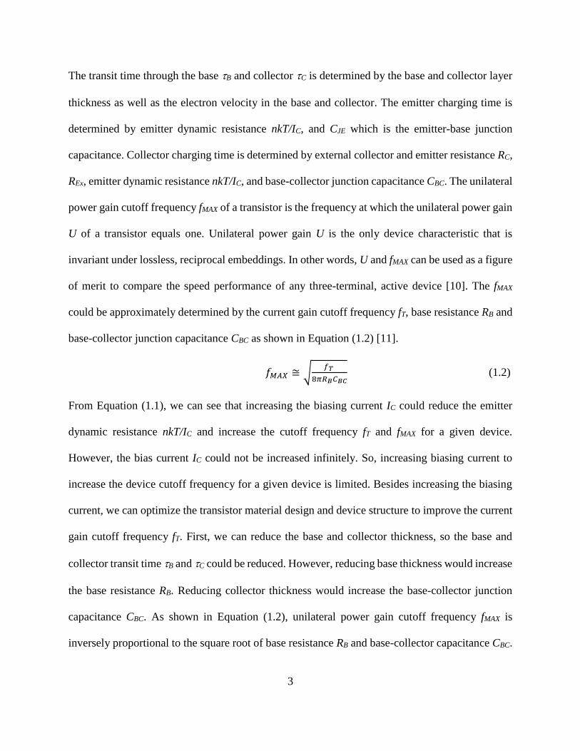
The transit time through the base B and collector C is determined by the base and collector layer
thickness as well as the electron velocity in the base and collector. The emitter charging time is
determined by emitter dynamic resistance nkT/IC, and CJE which is the emitter-base junction
capacitance. Collector charging time is determined by external collector and emitter resistance RC,
REx, emitter dynamic resistance nkT/IC, and base-collector junction capacitance CBC. The unilateral
power gain cutoff frequency fMAX of a transistor is the frequency at which the unilateral power gain
U of a transistor equals one. Unilateral power gain U is the only device characteristic that is
invariant under lossless, reciprocal embeddings. In other words, U and fMAX can be used as a figure
of merit to compare the speed performance of any three-terminal, active device [10]. The fMAX
could be approximately determined by the current gain cutoff frequency fT, base resistance RB and
base-collector junction capacitance CBC as shown in Equation (1.2) [11].
𝑓𝑀𝐴𝑋 ≅ √𝑓𝑇
8𝜋𝑅𝐵𝐶𝐵𝐶 (1.2)
From Equation (1.1), we can see that increasing the biasing current IC could reduce the emitter
dynamic resistance nkT/IC and increase the cutoff frequency fT and fMAX for a given device.
However, the bias current IC could not be increased infinitely. So, increasing biasing current to
increase the device cutoff frequency for a given device is limited. Besides increasing the biasing
current, we can optimize the transistor material design and device structure to improve the current
gain cutoff frequency fT. First, we can reduce the base and collector thickness, so the base and
collector transit time B and C could be reduced. However, reducing base thickness would increase
the base resistance RB. Reducing collector thickness would increase the base-collector junction
capacitance CBC. As shown in Equation (1.2), unilateral power gain cutoff frequency fMAX is
inversely proportional to the square root of base resistance RB and base-collector capacitance CBC.
4
In addition, reducing the collector thickness would reduce the breakdown voltage of the transistor,
which would limit the operational dynamic range of the device. So, there is a trade-off between fT
and fMAX in choosing the base and collector thicknesses. Besides the base and collector thickness,
the emitter-base junction capacitance CJE, external emitter resistance REx, and collector resistance
RC could also be reduced by choosing appropriate doping and semiconductor material.
1.3 Different Types of HBTs
Depending on different heterojunction band alignments, there are mainly three types of InP
HBTs, namely, InP SHBT, Type-I InP DHBT, and Type-II InP DHBT. We will give a short
discussion of the different types of HBTs in this section.
InP SHBT has a single heterojunction at emitter-base junction. It typically has a wider band
gap InP emitter and narrower band gap InGaAs base and collector. The University of Illinois at
Urbana-Champaign (UIUC) has led the advancement of InP SHBT cutoff frequency through sub-
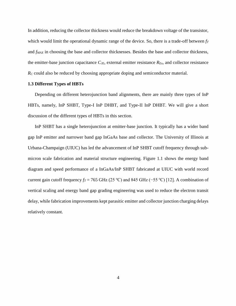
micron scale fabrication and material structure engineering. Figure 1.1 shows the energy band
diagram and speed performance of a InGaAs/InP SHBT fabricated at UIUC with world record
current gain cutoff frequency fT = 765 GHz (25 oC) and 845 GHz (−55 oC) [12]. A combination of
vertical scaling and energy band gap grading engineering was used to reduce the electron transit
delay, while fabrication improvements kept parasitic emitter and collector junction charging delays
relatively constant.
5
Figure 1.1: (a) Energy band diagram and (b) speed performance of a world record SHBT fabricated
at the Micro and Nanotechnology Laboratory (MNTL), UIUC.
Despite its high-speed capability, InP SHBT has low breakdown voltage, which limits its
operational dynamic range and output power. In order to increase the breakdown voltage, InP
DHBT technologies with both a wide band gap emitter and collector have been actively
investigated. Depending on different base-collector heterojunction band alignments, there are
mainly two types of InP DHBTs, namely, Type-I InP DHBT and Type-II InP DHBT. Type-I InP
DHBT has type-I band alignment for both emitter-base and base-collector heterojunctions. The
Type-I base-collector junction can block the current flow, which is known as the current-blocking
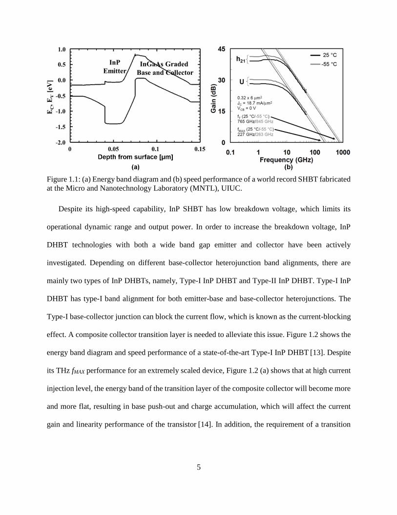
effect. A composite collector transition layer is needed to alleviate this issue. Figure 1.2 shows the
energy band diagram and speed performance of a state-of-the-art Type-I InP DHBT [13]. Despite
its THz fMAX performance for an extremely scaled device, Figure 1.2 (a) shows that at high current
injection level, the energy band of the transition layer of the composite collector will become more
and more flat, resulting in base push-out and charge accumulation, which will affect the current
gain and linearity performance of the transistor [14]. In addition, the requirement of a transition
6
layer complicates the transistor design, limits its vertical scalability, and lowers the breakdown
voltage compared with Type-II InP DHBT.
Figure 1.2: (a) Band diagram and (b) speed performance of a Type-I InP/InGaAs/InP DHBT.
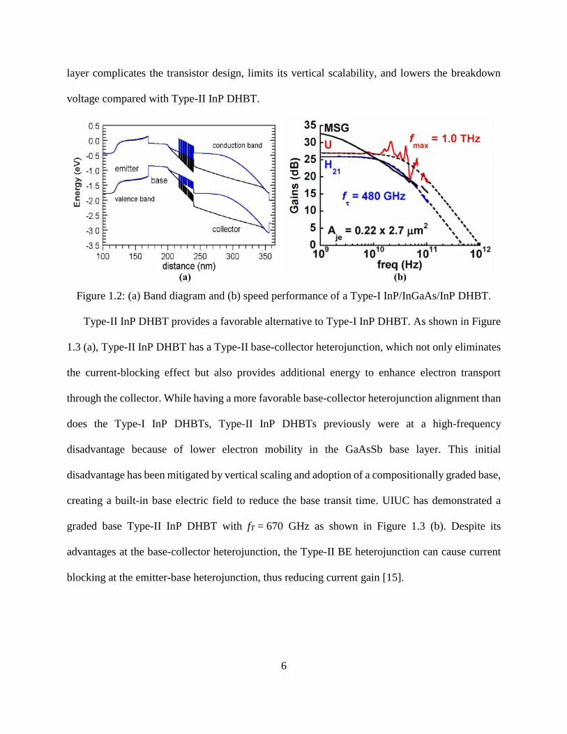
Type-II InP DHBT provides a favorable alternative to Type-I InP DHBT. As shown in Figure
1.3 (a), Type-II InP DHBT has a Type-II base-collector heterojunction, which not only eliminates
the current-blocking effect but also provides additional energy to enhance electron transport
through the collector. While having a more favorable base-collector heterojunction alignment than
does the Type-I InP DHBTs, Type-II InP DHBTs previously were at a high-frequency
disadvantage because of lower electron mobility in the GaAsSb base layer. This initial
disadvantage has been mitigated by vertical scaling and adoption of a compositionally graded base,
creating a built-in base electric field to reduce the base transit time. UIUC has demonstrated a
graded base Type-II InP DHBT with fT = 670 GHz as shown in Figure 1.3 (b). Despite its
advantages at the base-collector heterojunction, the Type-II BE heterojunction can cause current
blocking at the emitter-base heterojunction, thus reducing current gain [15].
7
Figure 1.3: (a) Energy band diagram and (b) high-frequency performance of a Type-II InP DHBT
fabricated at the UIUC.
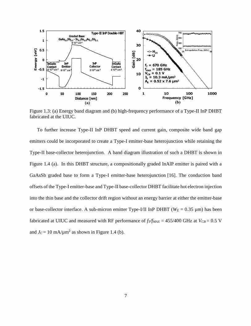
To further increase Type-II InP DHBT speed and current gain, composite wide band gap
emitters could be incorporated to create a Type-I emitter-base heterojunction while retaining the
Type-II base-collector heterojunction. A band diagram illustration of such a DHBT is shown in
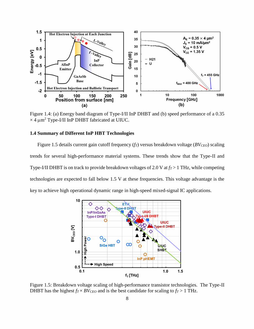
Figure 1.4 (a). In this DHBT structure, a compositionally graded InAlP emitter is paired with a
GaAsSb graded base to form a Type-I emitter-base heterojunction [16]. The conduction band
offsets of the Type-I emitter-base and Type-II base-collector DHBT facilitate hot electron injection
into the thin base and the collector drift region without an energy barrier at either the emitter-base
or base-collector interface. A sub-micron emitter Type-I/II InP DHBT (WE = 0.35 µm) has been
fabricated at UIUC and measured with RF performance of fT/fMAX = 455/400 GHz at VCB = 0.5 V
and JC = 10 mA/µm2 as shown in Figure 1.4 (b).
8
Figure 1.4: (a) Energy band diagram of Type-I/II InP DHBT and (b) speed performance of a 0.35
× 4 m2 Type-I/II InP DHBT fabricated at UIUC.
1.4 Summary of Different InP HBT Technologies
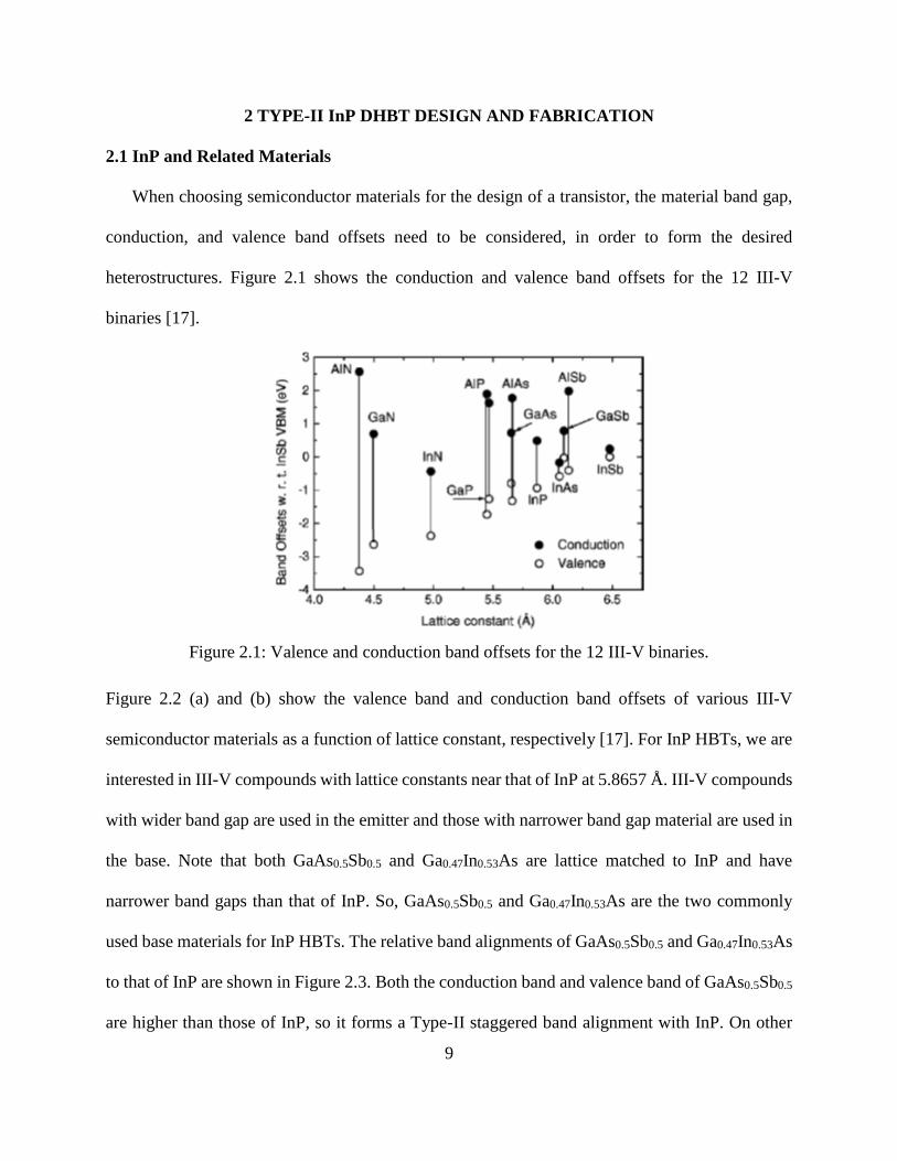
Figure 1.5 details current gain cutoff frequency (fT) versus breakdown voltage (BVCEO) scaling
trends for several high-performance material systems. These trends show that the Type-II and
Type-I/II DHBT is on track to provide breakdown voltages of 2.0 V at fT > 1 THz, while competing
technologies are expected to fall below 1.5 V at these frequencies. This voltage advantage is the
key to achieve high operational dynamic range in high-speed mixed-signal IC applications.
Figure 1.5: Breakdown voltage scaling of high-performance transistor technologies. The Type-II
DHBT has the highest fT × BVCEO and is the best candidate for scaling to fT > 1 THz.
9
2 TYPE-II InP DHBT DESIGN AND FABRICATION
2.1 InP and Related Materials
When choosing semiconductor materials for the design of a transistor, the material band gap,
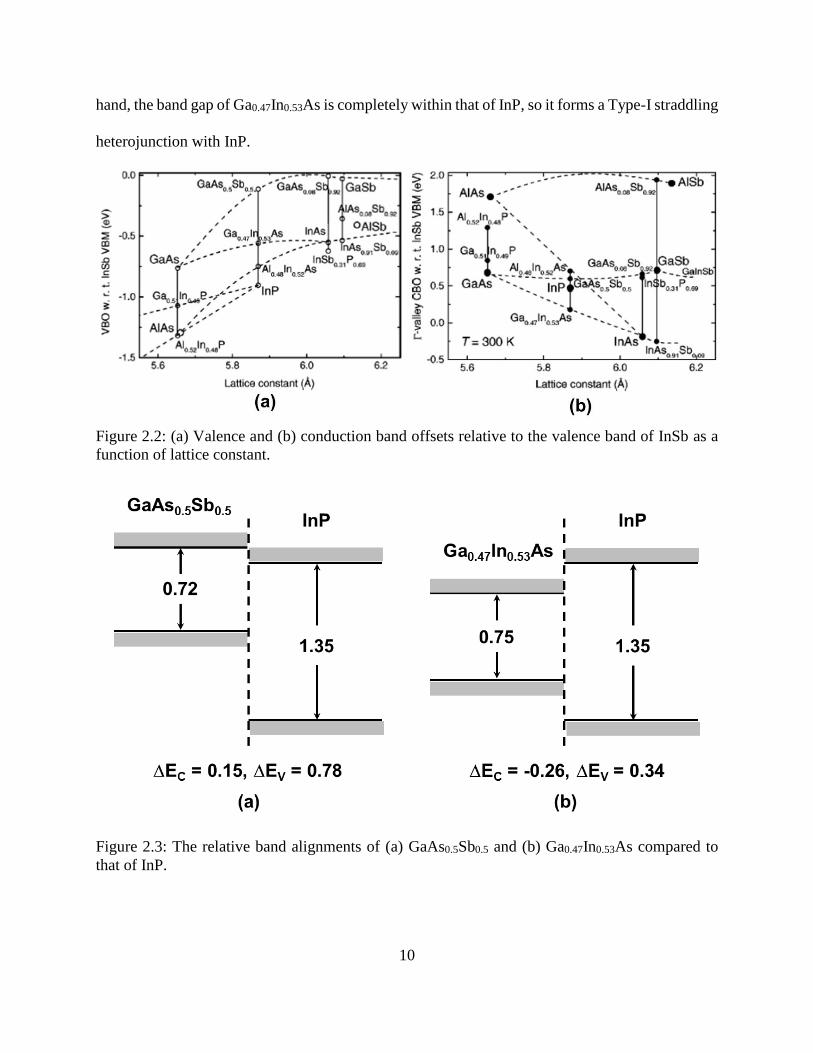
conduction, and valence band offsets need to be considered, in order to form the desired
heterostructures. Figure 2.1 shows the conduction and valence band offsets for the 12 III-V
binaries [17].
Figure 2.1: Valence and conduction band offsets for the 12 III-V binaries.
Figure 2.2 (a) and (b) show the valence band and conduction band offsets of various III-V
semiconductor materials as a function of lattice constant, respectively [17]. For InP HBTs, we are
interested in III-V compounds with lattice constants near that of InP at 5.8657 Å. III-V compounds
with wider band gap are used in the emitter and those with narrower band gap material are used in
the base. Note that both GaAs0.5Sb0.5 and Ga0.47In0.53As are lattice matched to InP and have
narrower band gaps than that of InP. So, GaAs0.5Sb0.5 and Ga0.47In0.53As are the two commonly
used base materials for InP HBTs. The relative band alignments of GaAs0.5Sb0.5 and Ga0.47In0.53As
to that of InP are shown in Figure 2.3. Both the conduction band and valence band of GaAs0.5Sb0.5
are higher than those of InP, so it forms a Type-II staggered band alignment with InP. On other
10
hand, the band gap of Ga0.47In0.53As is completely within that of InP, so it forms a Type-I straddling
heterojunction with InP.
Figure 2.2: (a) Valence and (b) conduction band offsets relative to the valence band of InSb as a
function of lattice constant.
Figure 2.3: The relative band alignments of (a) GaAs0.5Sb0.5 and (b) Ga0.47In0.53As compared to
that of InP.
11
2.2 Type-II InP DHBT Layer Structure Design
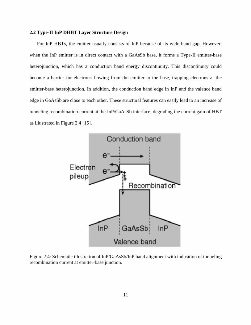
For InP HBTs, the emitter usually consists of InP because of its wide band gap. However,
when the InP emitter is in direct contact with a GaAsSb base, it forms a Type-II emitter-base
heterojunction, which has a conduction band energy discontinuity. This discontinuity could
become a barrier for electrons flowing from the emitter to the base, trapping electrons at the
emitter-base heterojunction. In addition, the conduction band edge in InP and the valence band
edge in GaAsSb are close to each other. These structural features can easily lead to an increase of
tunneling recombination current at the InP/GaAsSb interface, degrading the current gain of HBT
as illustrated in Figure 2.4 [15].
Figure 2.4: Schematic illustration of InP/GaAsSb/InP band alignment with indication of tunneling
recombination current at emitter-base junction.
12
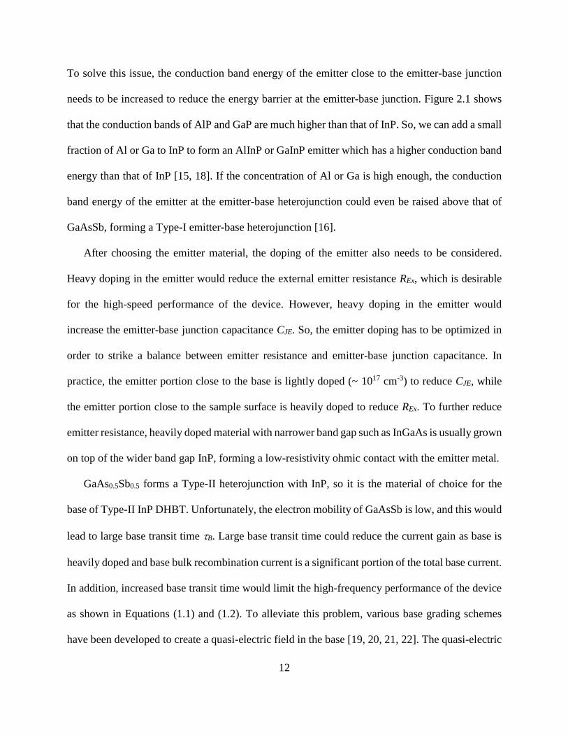
To solve this issue, the conduction band energy of the emitter close to the emitter-base junction
needs to be increased to reduce the energy barrier at the emitter-base junction. Figure 2.1 shows
that the conduction bands of AlP and GaP are much higher than that of InP. So, we can add a small
fraction of Al or Ga to InP to form an AlInP or GaInP emitter which has a higher conduction band
energy than that of InP [15, 18]. If the concentration of Al or Ga is high enough, the conduction
band energy of the emitter at the emitter-base heterojunction could even be raised above that of
GaAsSb, forming a Type-I emitter-base heterojunction [16].
After choosing the emitter material, the doping of the emitter also needs to be considered.
Heavy doping in the emitter would reduce the external emitter resistance REx, which is desirable
for the high-speed performance of the device. However, heavy doping in the emitter would
increase the emitter-base junction capacitance CJE. So, the emitter doping has to be optimized in
order to strike a balance between emitter resistance and emitter-base junction capacitance. In
practice, the emitter portion close to the base is lightly doped (~ 1017 cm-3) to reduce CJE, while
the emitter portion close to the sample surface is heavily doped to reduce REx. To further reduce
emitter resistance, heavily doped material with narrower band gap such as InGaAs is usually grown
on top of the wider band gap InP, forming a low-resistivity ohmic contact with the emitter metal.
GaAs0.5Sb0.5 forms a Type-II heterojunction with InP, so it is the material of choice for the
base of Type-II InP DHBT. Unfortunately, the electron mobility of GaAsSb is low, and this would
lead to large base transit time B. Large base transit time could reduce the current gain as base is
heavily doped and base bulk recombination current is a significant portion of the total base current.
In addition, increased base transit time would limit the high-frequency performance of the device
as shown in Equations (1.1) and (1.2). To alleviate this problem, various base grading schemes
have been developed to create a quasi-electric field in the base [19, 20, 21, 22]. The quasi-electric

13
field would accelerate the electrons in the base and thus reduce base transit time. Equations (2.1)
and (2.2) give the base transit time for a constant and graded base, respectively.
𝜏𝐵 =𝑇𝐵
2
2𝐷𝑛+
𝑇𝐵
𝑣𝑒𝑥𝑖𝑡 (2.1)
𝜏𝐵 =𝑘𝑇
𝐷𝑛∆𝐸[1 −
𝑘𝑇
∆𝐸(1 − 𝑒−
∆𝐸
𝑘𝑇)] 𝑇𝐵2 +
𝑘𝑇
𝑣𝑒𝑥𝑖𝑡∆𝐸(1 − 𝑒−
∆𝐸
𝑘𝑇)𝑇𝐵 (2.2)
The conventional base transit time expression is given by Equation (2.1) [9], and for a linear
graded base is modified as Equation (2.2) [23]. The second term in Equation (2.1) arises in the
short base because the finite exit velocity leads to a finite minority carrier concentration at the
collector edge of the base. Here, TB is the base thickness, Dn is the electron diffusion coefficient in
the base, ΔE is the total conduction band energy grade across the base, and vexit is the electron
velocity at the point where it exits the base. For example, a 200 Å base with Dn = 30 cm2/s and
base exit velocity 4 × 107 cm/s has 117 fs delay while the same base with a E = 50 meV linear
energy grading has 61 fs base delay. So, an energy grade of 50 meV can almost reduce the base
transit time by half, thus greatly improving device current gain and high-speed performance. The
base thickness also needs to be optimized. A thick base would reduce the base resistance RB, which
would increase the unilateral power gain cutoff frequency fMAX if fT is kept the same as shown in
Equation (1.2). However, as Equation (1.1) indicates, a thick base would increase base transit time
and thus reduce fT, which would in turn reduce fMAX. So, the base thickness needs to be optimized
to achieve a balanced performance of fT and fMAX.
The InP collector is usually lightly doped, so it could be depleted completely, leading to
reduced CBC. Keeping the collector doping level low also increases the breakdown voltage of the
transistor. However, the doping level of the collector cannot be kept too low, since it will limit the
current driving capability of a transistor. The biasing current of a transistor IC has to be kept high
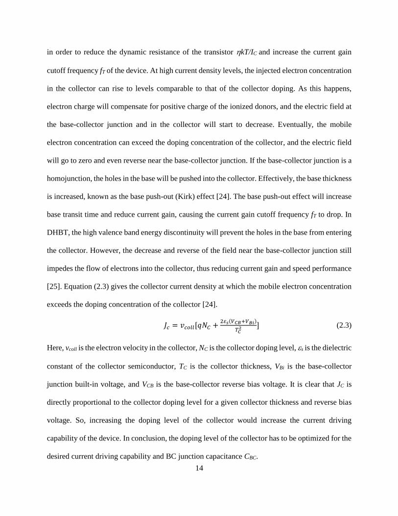
14
in order to reduce the dynamic resistance of the transistor kT/IC and increase the current gain
cutoff frequency fT of the device. At high current density levels, the injected electron concentration
in the collector can rise to levels comparable to that of the collector doping. As this happens,
electron charge will compensate for positive charge of the ionized donors, and the electric field at
the base-collector junction and in the collector will start to decrease. Eventually, the mobile
electron concentration can exceed the doping concentration of the collector, and the electric field
will go to zero and even reverse near the base-collector junction. If the base-collector junction is a
homojunction, the holes in the base will be pushed into the collector. Effectively, the base thickness
is increased, known as the base push-out (Kirk) effect [24]. The base push-out effect will increase
base transit time and reduce current gain, causing the current gain cutoff frequency fT to drop. In
DHBT, the high valence band energy discontinuity will prevent the holes in the base from entering
the collector. However, the decrease and reverse of the field near the base-collector junction still
impedes the flow of electrons into the collector, thus reducing current gain and speed performance
[25]. Equation (2.3) gives the collector current density at which the mobile electron concentration
exceeds the doping concentration of the collector [24].
𝐽𝑐 = 𝑣𝑐𝑜𝑙𝑙[𝑞𝑁𝐶 +2𝜀𝑠(𝑉𝐶𝐵+𝑉𝐵𝑖)
𝑇𝐶2 ] (2.3)
Here, vcoll is the electron velocity in the collector, NC is the collector doping level, s is the dielectric
constant of the collector semiconductor, TC is the collector thickness, VBi is the base-collector
junction built-in voltage, and VCB is the base-collector reverse bias voltage. It is clear that JC is
directly proportional to the collector doping level for a given collector thickness and reverse bias
voltage. So, increasing the doping level of the collector would increase the current driving
capability of the device. In conclusion, the doping level of the collector has to be optimized for the
desired current driving capability and BC junction capacitance CBC.
15
2.3 Sub-Micron DHBT Fabrication Process
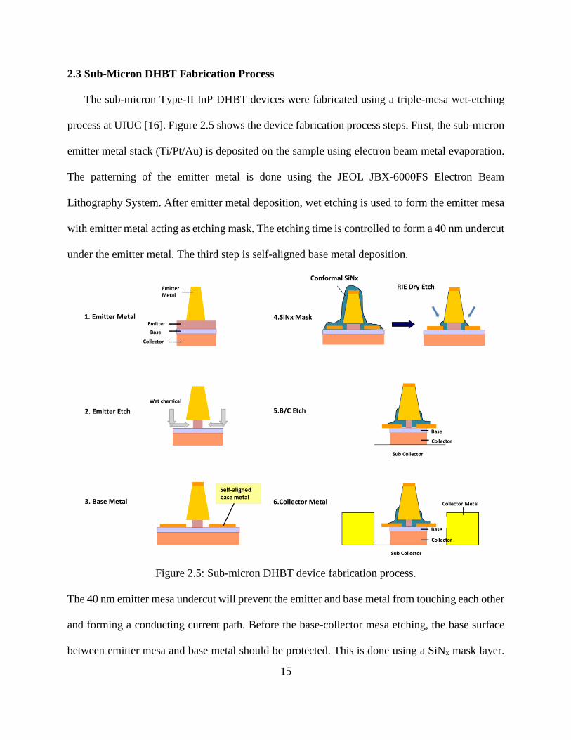
The sub-micron Type-II InP DHBT devices were fabricated using a triple-mesa wet-etching
process at UIUC [16]. Figure 2.5 shows the device fabrication process steps. First, the sub-micron
emitter metal stack (Ti/Pt/Au) is deposited on the sample using electron beam metal evaporation.
The patterning of the emitter metal is done using the JEOL JBX-6000FS Electron Beam
Lithography System. After emitter metal deposition, wet etching is used to form the emitter mesa
with emitter metal acting as etching mask. The etching time is controlled to form a 40 nm undercut
under the emitter metal. The third step is self-aligned base metal deposition.
Figure 2.5: Sub-micron DHBT device fabrication process.
The 40 nm emitter mesa undercut will prevent the emitter and base metal from touching each other
and forming a conducting current path. Before the base-collector mesa etching, the base surface
between emitter mesa and base metal should be protected. This is done using a SiNx mask layer.
16
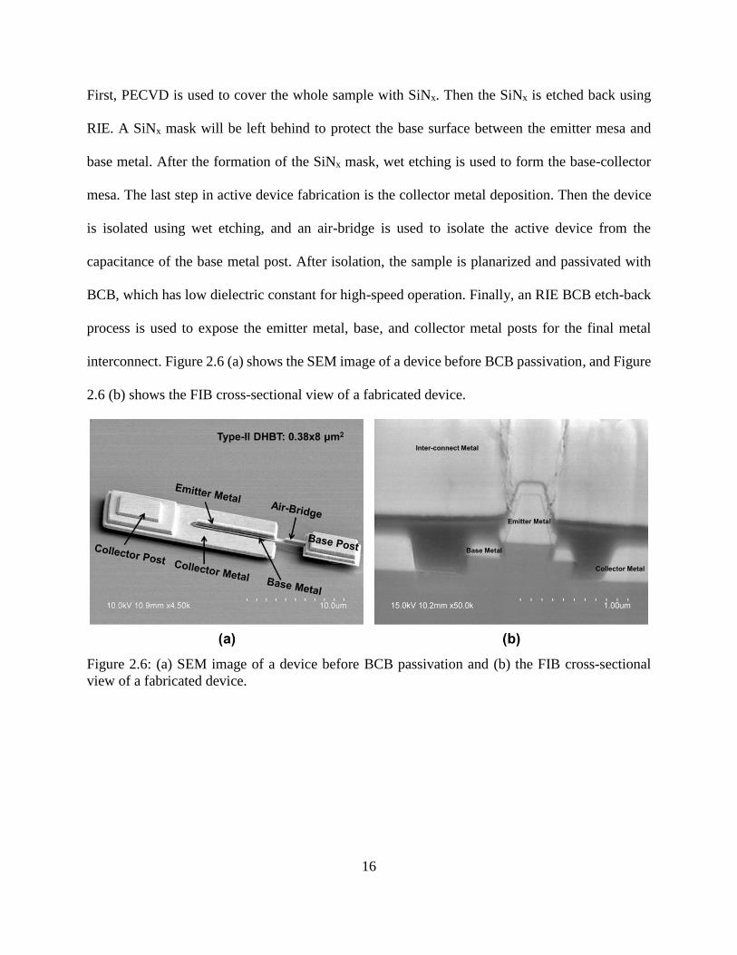
First, PECVD is used to cover the whole sample with SiNx. Then the SiNx is etched back using
RIE. A SiNx mask will be left behind to protect the base surface between the emitter mesa and
base metal. After the formation of the SiNx mask, wet etching is used to form the base-collector
mesa. The last step in active device fabrication is the collector metal deposition. Then the device
is isolated using wet etching, and an air-bridge is used to isolate the active device from the
capacitance of the base metal post. After isolation, the sample is planarized and passivated with
BCB, which has low dielectric constant for high-speed operation. Finally, an RIE BCB etch-back
process is used to expose the emitter metal, base, and collector metal posts for the final metal
interconnect. Figure 2.6 (a) shows the SEM image of a device before BCB passivation, and Figure
2.6 (b) shows the FIB cross-sectional view of a fabricated device.
Figure 2.6: (a) SEM image of a device before BCB passivation and (b) the FIB cross-sectional
view of a fabricated device.
17
2.4 Scaling of Sub-Micron DHBT
Transistors could be scaled down vertically and laterally in order to increase the current gain
cutoff frequency fT and unilateral power gain cutoff frequency fMAX [23]. The current gain cutoff
frequency fT is inversely proportional to the total delay of the transistor as shown in Equation (1.1).
Vertically scaling the device to reduce the base and collector thickness would reduce the base and
collector transit time, thus increasing fT. Currently, high-speed InP DHBTs usually have a base
thickness of about 20 nm, and collector thickness of about 120 nm. Although vertical scaling can
increase fT, it may not be able to increase fMAX when the base and collector layer thickness has been
reduced to a certain point. As shown in Equation (1.2), fMAX is proportional to the square root of fT
and inversely proportional to the square root of base resistance RB and base-collector capacitance
CBC. So, when the base and collector thickness is reduced, fMAX will first increase as fT is increased
due to reduced base and collector transit time. However, as base and collector thickness is further
reduced, the base resistance RB and base-collector capacitance CBC will increase dramatically. So,
the fMAX will decrease as the base and collector thickness is further scaled down. As a result, to
maximize the speed performance of the transistor, detailed analysis and optimization of base and
collector thickness need to be done to find the optimum thickness [26, 27].
Besides vertical scaling, lateral scaling the fabricated device dimensions could be used to
reduce resistances and capacitances of the device, thus improving device speed performance.
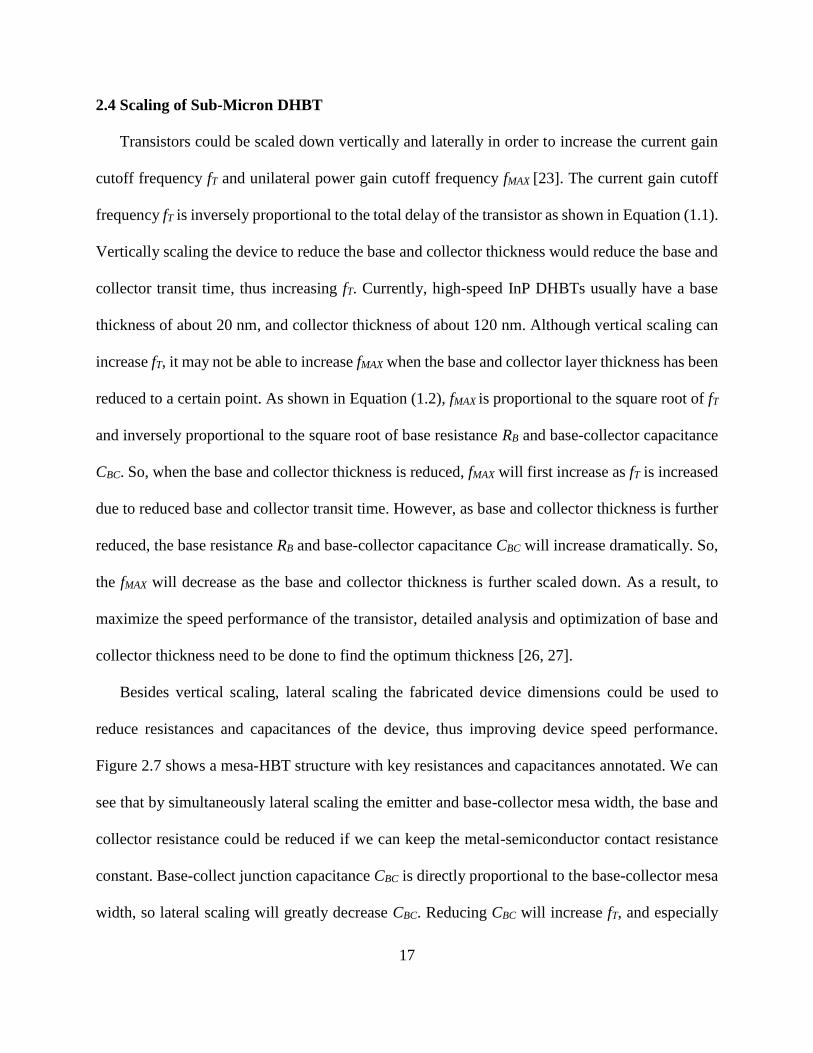
Figure 2.7 shows a mesa-HBT structure with key resistances and capacitances annotated. We can
see that by simultaneously lateral scaling the emitter and base-collector mesa width, the base and
collector resistance could be reduced if we can keep the metal-semiconductor contact resistance
constant. Base-collect junction capacitance CBC is directly proportional to the base-collector mesa
width, so lateral scaling will greatly decrease CBC. Reducing CBC will increase fT, and especially
18
fMAX, which is inversely proportional to the square root of RB times CBC. It is estimated that when
lateral scaling is done properly, fMAX would be inversely proportional to the square root of emitter
WE (𝑓𝑀𝐴𝑋 ∝ √1/𝑊𝐸 ) [23]. In 2011, fT/fMAX performance of 521/1150 GHz was reported for a
deeply scaled down 0.13 × 2 μm2 Type-I InP DHBT [13]. In 2013, composition-graded GaAsSb
base Type-II InP DHBT had reported power gain cutoff frequency fMAX = 621 GHz for a 0.2 × 4.4
μm2 device [28].
Figure 2.7: Illustration of current mesa-HBT structure with key resistances and capacitances
annotated.
19
3 CHARACTERIZATION AND COMPARISON OF TYPE-I AND TYPE-I/II InP DHBTs
To study the advantages of Type-II BC band alignment, the DC, RF, and nonlinearity
performances of a Type-I/II InP DHBT have been characterized and compared with that of a
foundry provided Type-I InP DHBT. The layer structures of the Type-I and Type-I/II InP DHBTs
studied in this work are shown in Table 3.1 [14]. The foundry-provided Type-I InP/InGaAs/InP
DHBT uses an InGaAs collector super-lattice transition layer to alleviate the current-blocking
effect [29, 30].
Table 3.1: Layer structures for Type-I InGaAs DHBT and Type-I/II GaAsSb DHBT.
3.1 DC Characterization of InP DHBTs
The DC characterization of a device is done using a HP 4142B DC source/monitor. The
measurement setup is shown in Figure 3.1. The family curve is measured by setting a base bias
current and sweeping the collector-emitter voltage. After each collector-emitter voltage sweep, the
base bias current is increased. Figure 3.2 (a) shows the family I-V curves of Type-I/II
AlInP/GaAsSb/InP and Type-I InP/InGaAs/InP DHBT. The knee voltage of Type-I/II
AlInP/GaAsSb/InP DHBT is lower than that of Type-I InP/InGaAs/InP DHBT, especially at high
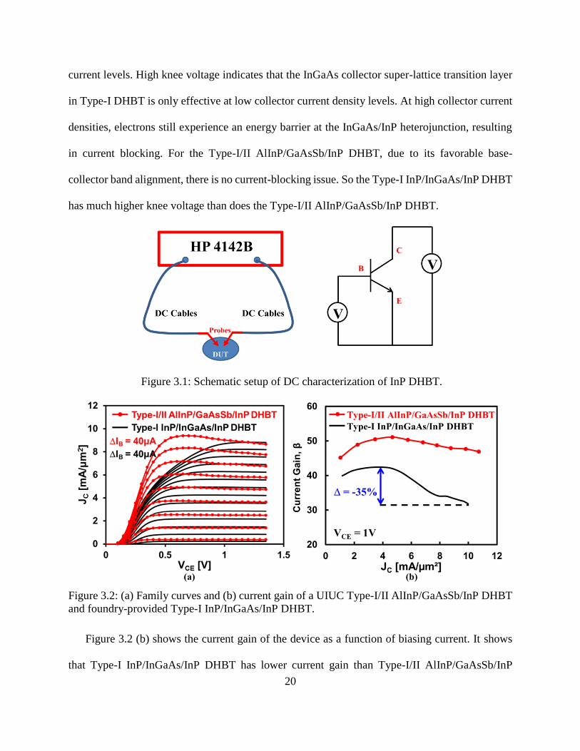
20
current levels. High knee voltage indicates that the InGaAs collector super-lattice transition layer
in Type-I DHBT is only effective at low collector current density levels. At high collector current
densities, electrons still experience an energy barrier at the InGaAs/InP heterojunction, resulting
in current blocking. For the Type-I/II AlInP/GaAsSb/InP DHBT, due to its favorable base-
collector band alignment, there is no current-blocking issue. So the Type-I InP/InGaAs/InP DHBT
has much higher knee voltage than does the Type-I/II AlInP/GaAsSb/InP DHBT.
Figure 3.1: Schematic setup of DC characterization of InP DHBT.
Figure 3.2: (a) Family curves and (b) current gain of a UIUC Type-I/II AlInP/GaAsSb/InP DHBT
and foundry-provided Type-I InP/InGaAs/InP DHBT.
Figure 3.2 (b) shows the current gain of the device as a function of biasing current. It shows
that Type-I InP/InGaAs/InP DHBT has lower current gain than Type-I/II AlInP/GaAsSb/InP
21
DHBT. More importantly, Type-I InP/InGaAs/InP DHBT shows more than 35% current gain ()
drop at high current densities, while the variance of Type-I/II AlInP/GaAsSb/InP DHBT is less
than 10%. The high current gain compression and high knee voltage in Type-I InP/InGaAs/InP
DHBT will result in nonlinear effects and narrower dynamic range, which affects its potential for
mixed-signal IC applications [14].
3.2 RF Characterization of InP DHBTs
RF characterization of a device was done using an Agilent 8364A network analyzer. Off-wafer
calibration of the network analyzer is done using a standard calibration substrate. On-wafer short
and open standards were used to de-embed the probe inductance and capacitance from the
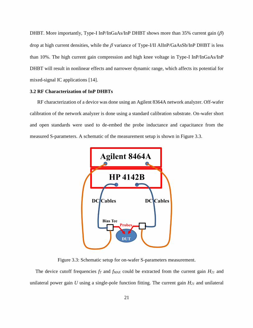
measured S-parameters. A schematic of the measurement setup is shown in Figure 3.3.
Figure 3.3: Schematic setup for on-wafer S-parameters measurement.
The device cutoff frequencies fT and fMAX could be extracted from the current gain H21 and
unilateral power gain U using a single-pole function fitting. The current gain H21 and unilateral
22
power gain U is calculated from measured S-parameters of the device using Equations (3.1) and
(3.2).
𝐻21 =−2𝑆21
(1−𝑆11)(1+𝑆22)+𝑆12𝑆21 (3.1)
𝑈 =|𝑌21−𝑌12|2
4(𝑅𝑒[𝑌11]𝑅𝑒[𝑌22]−𝑅𝑒[𝑌12]𝑅𝑒[𝑌21]) (3.2)
𝑌11 =(1−𝑆11)(1+𝑆22)+𝑆12𝑆21
∆ (3.3)
𝑌12 =−2𝑆12
∆ (3.4)
𝑌21 =−2𝑆21
∆ (3.5)
𝑌22 =(1+𝑆11)(1−𝑆22)+𝑆12𝑆21
∆ (3.6)
∆= (1 + 𝑆11)(1 + 𝑆22) − 𝑆12𝑆21 (3.7)
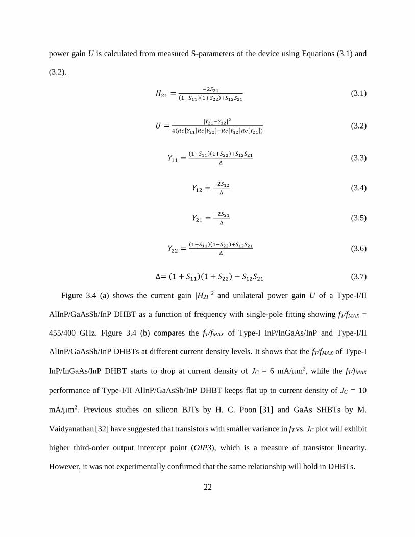
Figure 3.4 (a) shows the current gain |H21|2 and unilateral power gain U of a Type-I/II
AlInP/GaAsSb/InP DHBT as a function of frequency with single-pole fitting showing fT/fMAX =
455/400 GHz. Figure 3.4 (b) compares the fT/fMAX of Type-I InP/InGaAs/InP and Type-I/II
AlInP/GaAsSb/InP DHBTs at different current density levels. It shows that the fT/fMAX of Type-I
InP/InGaAs/InP DHBT starts to drop at current density of JC = 6 mA/m2, while the fT/fMAX
performance of Type-I/II AlInP/GaAsSb/InP DHBT keeps flat up to current density of JC = 10
mA/m2. Previous studies on silicon BJTs by H. C. Poon [31] and GaAs SHBTs by M.
Vaidyanathan [32] have suggested that transistors with smaller variance in fT vs. JC plot will exhibit
higher third-order output intercept point (OIP3), which is a measure of transistor linearity.
However, it was not experimentally confirmed that the same relationship will hold in DHBTs.
23
Figure 3.4: (a) The current gain |H21|2 and unilateral power gain U of a Type-I/II
AlInP/GaAsSb/InP DHBT and (b) the fT/fMAX performance of a Type-I InP/InGaAs/InP and Type-
I/II AlInP/GaAsSb/InP DHBT.
3.3 Nonlinearity Characterization of InP DHBTs
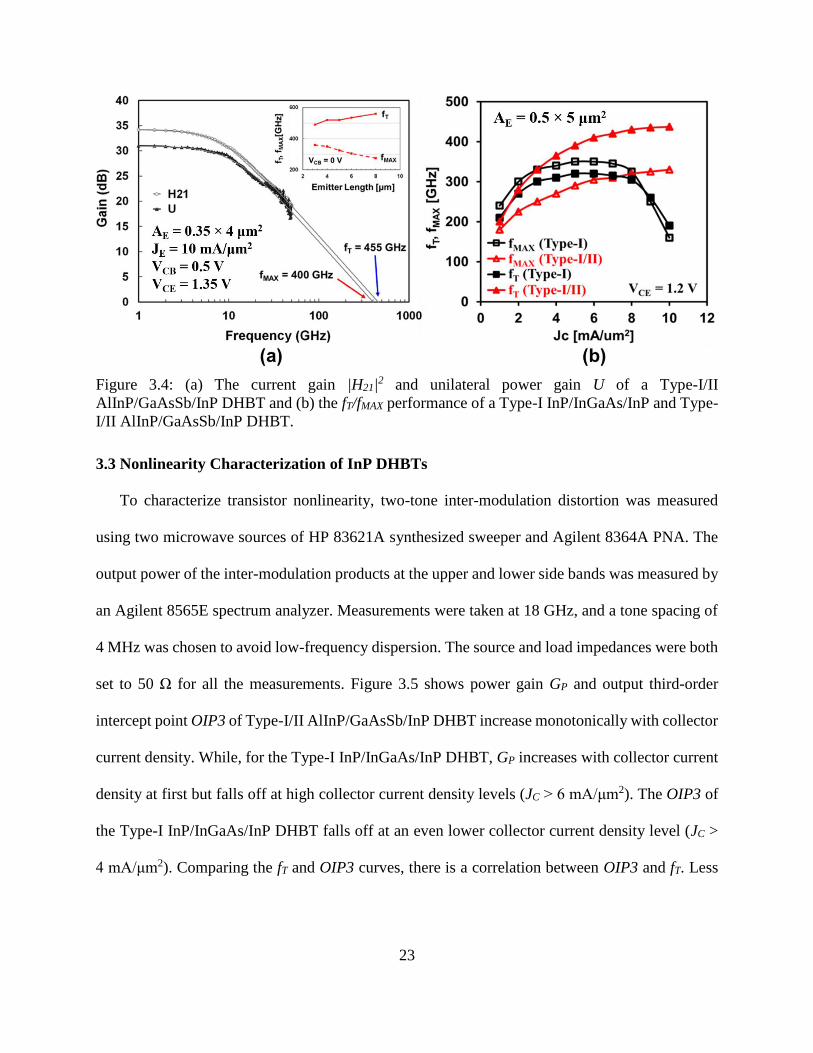
To characterize transistor nonlinearity, two-tone inter-modulation distortion was measured
using two microwave sources of HP 83621A synthesized sweeper and Agilent 8364A PNA. The
output power of the inter-modulation products at the upper and lower side bands was measured by
an Agilent 8565E spectrum analyzer. Measurements were taken at 18 GHz, and a tone spacing of
4 MHz was chosen to avoid low-frequency dispersion. The source and load impedances were both
set to 50 Ω for all the measurements. Figure 3.5 shows power gain GP and output third-order
intercept point OIP3 of Type-I/II AlInP/GaAsSb/InP DHBT increase monotonically with collector
current density. While, for the Type-I InP/InGaAs/InP DHBT, GP increases with collector current
density at first but falls off at high collector current density levels (JC > 6 mA/μm2). The OIP3 of
the Type-I InP/InGaAs/InP DHBT falls off at an even lower collector current density level (JC >
4 mA/μm2). Comparing the fT and OIP3 curves, there is a correlation between OIP3 and fT. Less
24
variant, monotonically increasing fT will lead to higher OIP3 (superior linearity), and fT with more
variance will lead to lower OIP3 (inferior linearity).
Figure 3.5: The power gain GP and the third-order output intercept point OIP3 of Type-I
InP/InGaAs/InP and Type-I/II AlInP/GaAsSb/InP DHBTs.
3.4 Physical Origins of Nonlinearity
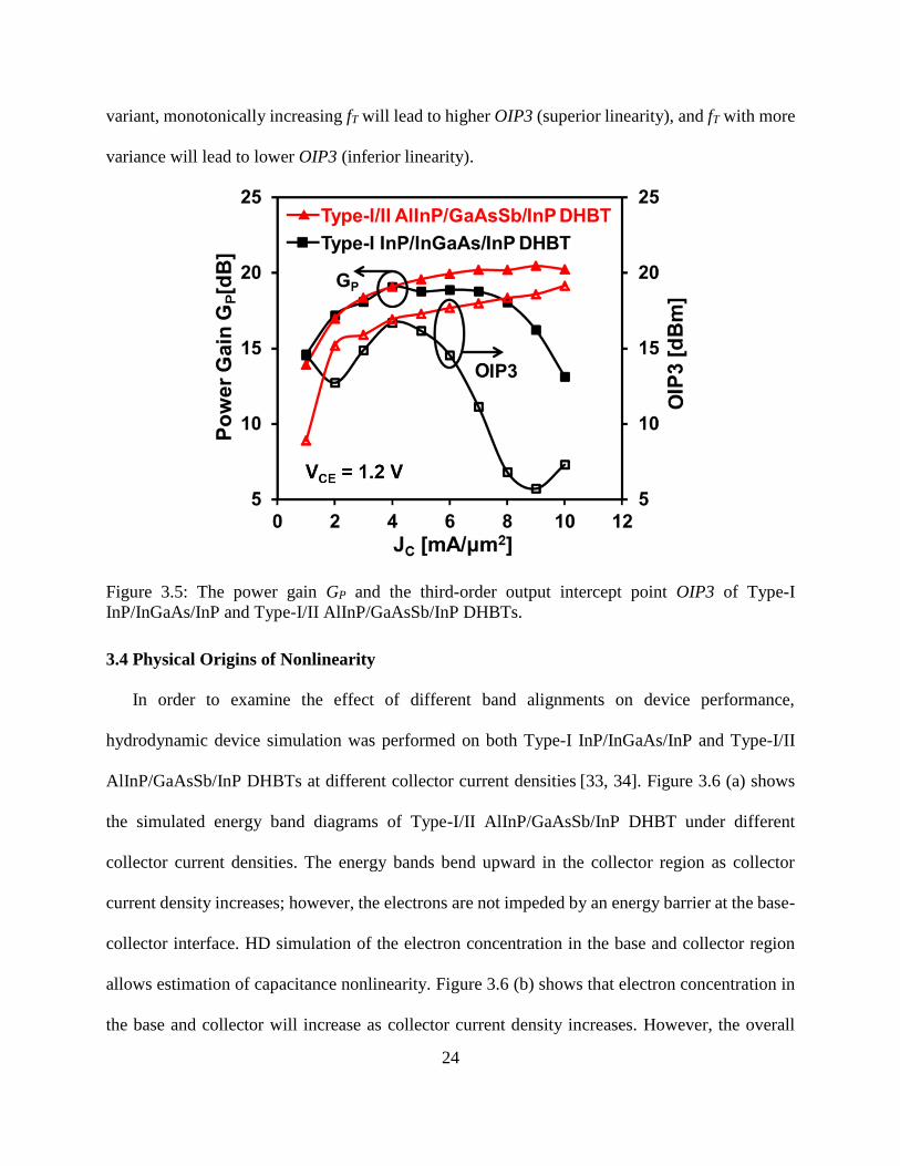
In order to examine the effect of different band alignments on device performance,
hydrodynamic device simulation was performed on both Type-I InP/InGaAs/InP and Type-I/II
AlInP/GaAsSb/InP DHBTs at different collector current densities [33, 34]. Figure 3.6 (a) shows
the simulated energy band diagrams of Type-I/II AlInP/GaAsSb/InP DHBT under different
collector current densities. The energy bands bend upward in the collector region as collector
current density increases; however, the electrons are not impeded by an energy barrier at the base-
collector interface. HD simulation of the electron concentration in the base and collector region
allows estimation of capacitance nonlinearity. Figure 3.6 (b) shows that electron concentration in
the base and collector will increase as collector current density increases. However, the overall
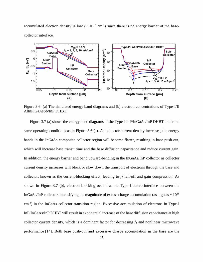
25
accumulated electron density is low (~ 1017 cm-3) since there is no energy barrier at the base-
collector interface.
Figure 3.6: (a) The simulated energy band diagrams and (b) electron concentrations of Type-I/II
AlInP/GaAsSb/InP DHBT.
Figure 3.7 (a) shows the energy band diagrams of the Type-I InP/InGaAs/InP DHBT under the
same operating conditions as in Figure 3.6 (a). As collector current density increases, the energy
bands in the InGaAs composite collector region will become flatter, resulting in base push-out,
which will increase base transit time and the base diffusion capacitance and reduce current gain.
In addition, the energy barrier and band upward-bending in the InGaAs/InP collector as collector
current density increases will block or slow down the transport of electrons through the base and
collector, known as the current-blocking effect, leading to fT fall-off and gain compression. As
shown in Figure 3.7 (b), electron blocking occurs at the Type-I hetero-interface between the
InGaAs/InP collector, intensifying the magnitude of excess charge accumulation (as high as ~ 1018
cm-3) in the InGaAs collector transition region. Excessive accumulation of electrons in Type-I
InP/InGaAs/InP DHBT will result in exponential increase of the base diffusion capacitance at high
collector current density, which is a dominant factor for decreasing fT and nonlinear microwave
performance [14]. Both base push-out and excessive charge accumulation in the base are the
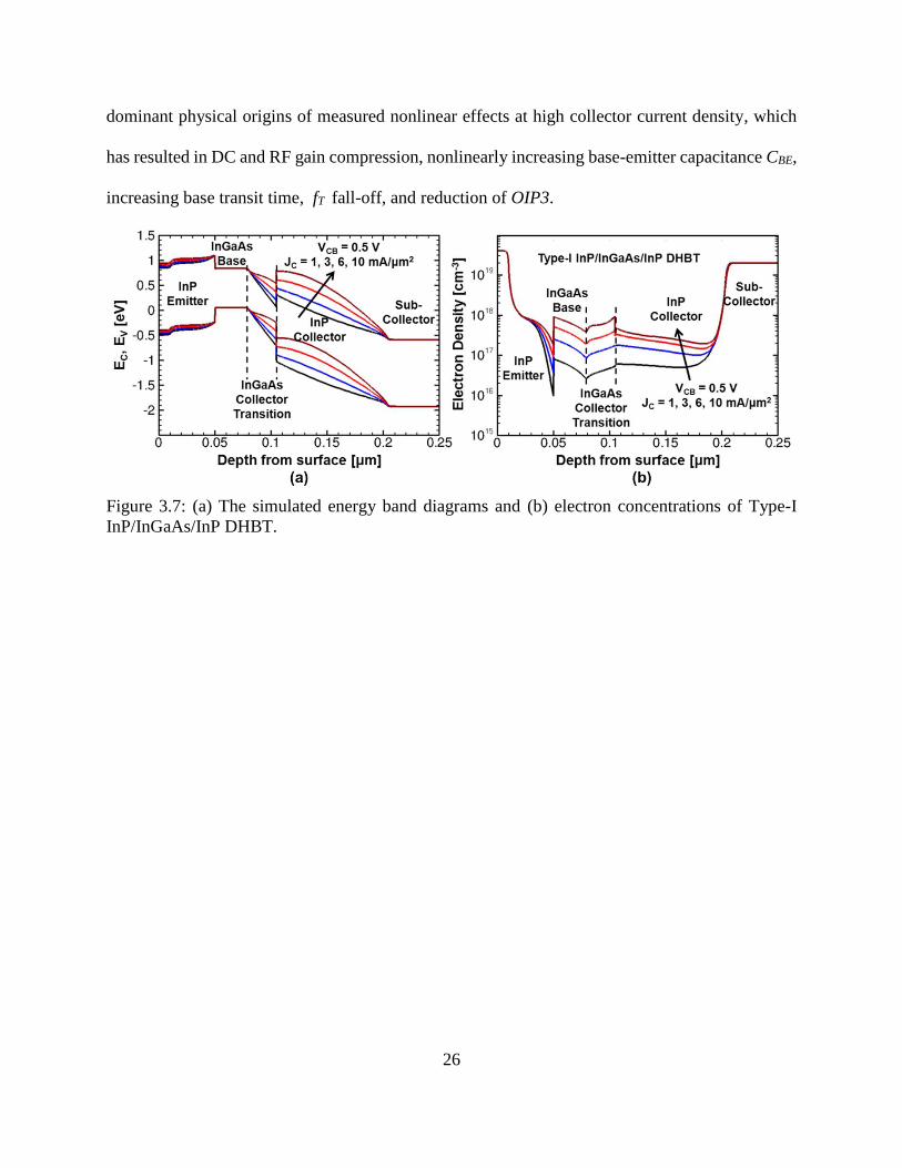
26
dominant physical origins of measured nonlinear effects at high collector current density, which
has resulted in DC and RF gain compression, nonlinearly increasing base-emitter capacitance CBE,
increasing base transit time, fT fall-off, and reduction of OIP3.
Figure 3.7: (a) The simulated energy band diagrams and (b) electron concentrations of Type-I
InP/InGaAs/InP DHBT.
27
4 COMPOSITION-GRADED AlGaAsSb BASE TYPE-II InP DHBT
4.1 Composition-Graded AlGaAsSb Base Type-II InP DHBT Layer Structure
The base of Type-II InP DHBT needs to be graded in order to create a quasi-electric field to
accelerate the electrons through the base in order to reduce the base transit time and increase
current gain. Composition-graded InxGa1-xAsySb1-y and GaAsxSb1-x are two of the commonly used
base materials [19, 20, 28]. The InxGa1-xAsySb1-y Type-II DHBT has exhibited the highest fT = 670
GHz, with fMAX = 185 GHz for a 0.52 × 7.6 m2 device, biased at JE = 10.3 mA/m2 and VCB = 0.1
V [26], while the GaAsSb Type-II DHBT exhibited the best fMAX = 621 GHz, with fT = 428 GHz
for a 0.2 × 4.4 m2 device, biased at IC = 7.6 mA and VCE = 1.2 V [28]. However, the degree of
composition grading of GaxAs1-xSb and InxGa1-xAsySb1-y is limited because these materials are not
lattice matched to the InP substrate. Recently, AlxGa1-xAsySb1-y has been investigated as a base
material for Type-II InP DHBTs [21, 35]. AlxGa1-xAsySb1-y can provide a steeper band gap grading
in the base while maintaining a lattice match to InP, which offers great potential for high-frequency
performance. To date, only DC data of large area devices has been reported for this material
system. In this work, composition-graded AlxGa1-xAsySb1-y DHBTs with 0.3 m emitter width
were designed, fabricated, and demonstrated with high-frequency operation capability [36].
Devices also demonstrate peak current gain = 20 and breakdown voltage BVCEO > 5.0 V. A 0.3
× 2 m2 device shows fMAX = 510 GHz with fT = 450 GHz at JE = 10 mA/μm2 and VCB = 0.2 V.
The energy band diagram of the DHBT layer structure was designed and calculated using
model solid theory and material band gap parameters from Vurgaftman [17]. As shown in Figure
4.1, the composition-graded AlxGa1-xAsySb1-y base creates a band gap difference Eg ≈ 135 meV
between the emitter side and the collector side of the base.
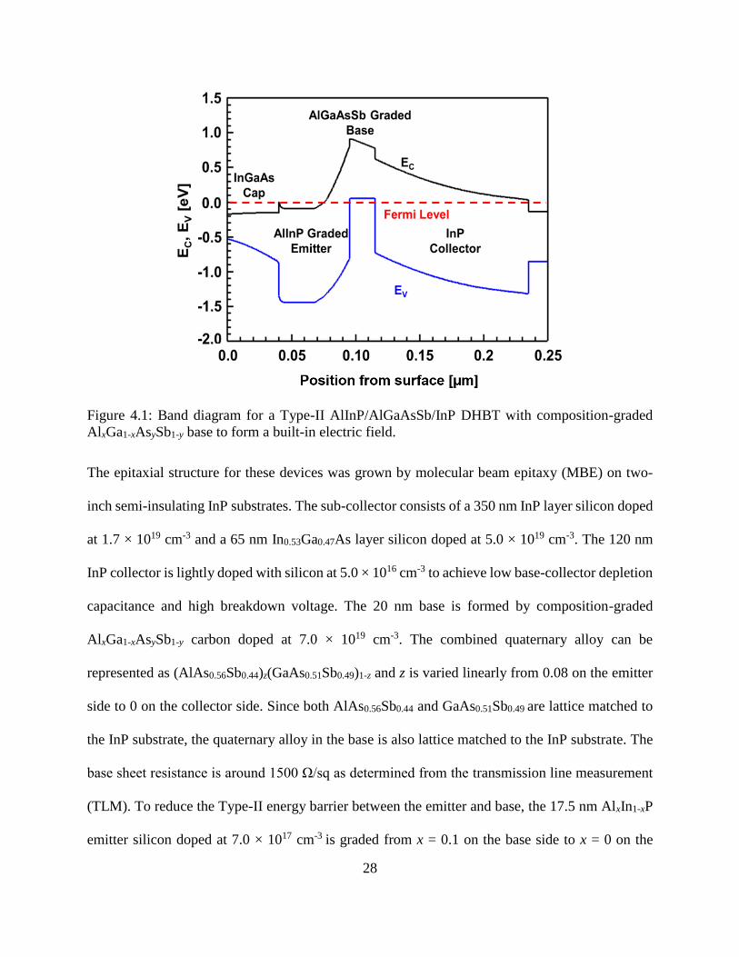
28
Figure 4.1: Band diagram for a Type-II AlInP/AlGaAsSb/InP DHBT with composition-graded
AlxGa1-xAsySb1-y base to form a built-in electric field.
The epitaxial structure for these devices was grown by molecular beam epitaxy (MBE) on two-
inch semi-insulating InP substrates. The sub-collector consists of a 350 nm InP layer silicon doped
at 1.7 × 1019 cm-3 and a 65 nm In0.53Ga0.47As layer silicon doped at 5.0 × 1019 cm-3. The 120 nm
InP collector is lightly doped with silicon at 5.0 × 1016 cm-3 to achieve low base-collector depletion
capacitance and high breakdown voltage. The 20 nm base is formed by composition-graded
AlxGa1-xAsySb1-y carbon doped at 7.0 × 1019 cm-3. The combined quaternary alloy can be
represented as (AlAs0.56Sb0.44)z(GaAs0.51Sb0.49)1-z and z is varied linearly from 0.08 on the emitter
side to 0 on the collector side. Since both AlAs0.56Sb0.44 and GaAs0.51Sb0.49 are lattice matched to
the InP substrate, the quaternary alloy in the base is also lattice matched to the InP substrate. The
base sheet resistance is around 1500 Ω/sq as determined from the transmission line measurement
(TLM). To reduce the Type-II energy barrier between the emitter and base, the 17.5 nm AlxIn1-xP
emitter silicon doped at 7.0 × 1017 cm-3 is graded from x = 0.1 on the base side to x = 0 on the
29
emitter surface side. A 7.5 nm InP layer silicon doped at 3.0 × 1018 cm-3 is inserted as a doping
transition layer followed by a 30 nm InP emitter silicon doped at 1.7 × 1019 cm-3. The emitter
contact layer consists of a 5 nm In0.53Ga0.47As layer and a 35 nm In0.53Ga0.47As graded to an InAs
layer, both silicon doped at 5 × 1019 cm-3.
4.2 DC and RF Performance of Graded AlGaAsSb Base Type-II InP DHBT
Devices with emitter width 0.3 µm and lengths ranging from 2 to 8 µm were fabricated using
a triple-mesa wet-etching process with metal contacts defined by electron beam lithography. An
air-bridge was used in order to isolate the device from the capacitance associated with the base-
post pad. A benzocyclobutene (BCB) based etch-back process was used to expose the emitter
contact, as well as the base and collector posts for the final metal interconnect. The measured
contact resistivity of the collector is 30 Ω/μm2, and the access resistivity of the emitter is 8 Ω-μm2.
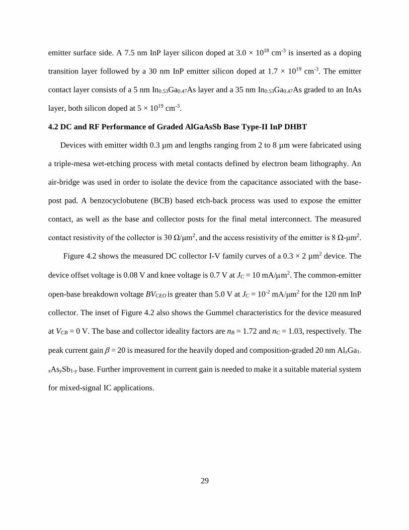
Figure 4.2 shows the measured DC collector I-V family curves of a 0.3 × 2 µm2 device. The
device offset voltage is 0.08 V and knee voltage is 0.7 V at JC = 10 mA/m2. The common-emitter
open-base breakdown voltage BVCEO is greater than 5.0 V at JC = 10-2 mA/μm2 for the 120 nm InP
collector. The inset of Figure 4.2 also shows the Gummel characteristics for the device measured
at VCB = 0 V. The base and collector ideality factors are nB = 1.72 and nC = 1.03, respectively. The
peak current gain = 20 is measured for the heavily doped and composition-graded 20 nm AlxGa1-
xAsySb1-y base. Further improvement in current gain is needed to make it a suitable material system
for mixed-signal IC applications.
30
Figure 4.2: Collector I-V characteristics for a 0.3 × 2 m2 DHBT. Inset: Gummel characteristics
of the same device measured with VCB = 0 V.
The device microwave performance was measured from S-parameters taken from 0.5 GHz to
50 GHz using an Agilent 8364A PNA. A short-open-load-through (SOLT) calibration was
performed for the PNA using a Cascade impedance standard substrate. On-wafer short and open
fixtures were measured to de-embed the probe pad inductance and capacitance from the devices’
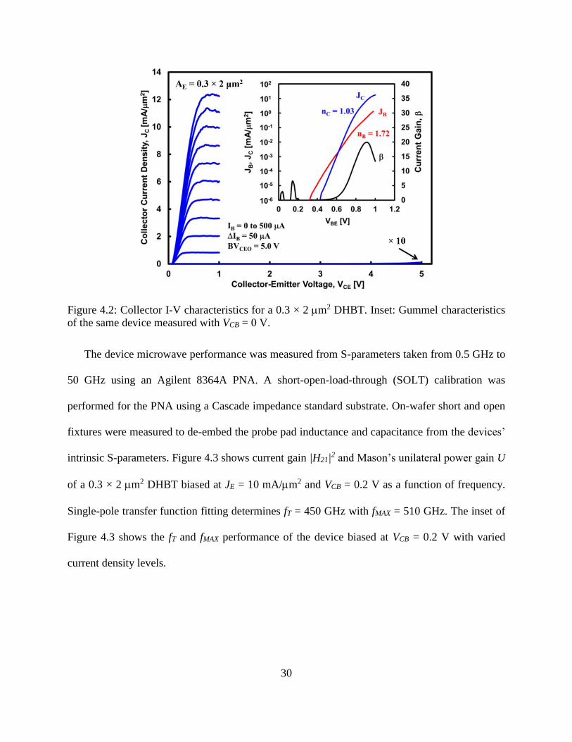
intrinsic S-parameters. Figure 4.3 shows current gain |H21|2 and Mason’s unilateral power gain U
of a 0.3 × 2 m2 DHBT biased at JE = 10 mA/m2 and VCB = 0.2 V as a function of frequency.
Single-pole transfer function fitting determines fT = 450 GHz with fMAX = 510 GHz. The inset of
Figure 4.3 shows the fT and fMAX performance of the device biased at VCB = 0.2 V with varied
current density levels.
31
Figure 4.3: Current gain |H21|2 and Mason’s unilateral power gain U as a function of frequency
showing fT and fMAX extrapolated with single-pole transfer function fitting. Inset: fT and fMAX
performance of the device biased at VCB = 0.2 V and different collector current density levels.
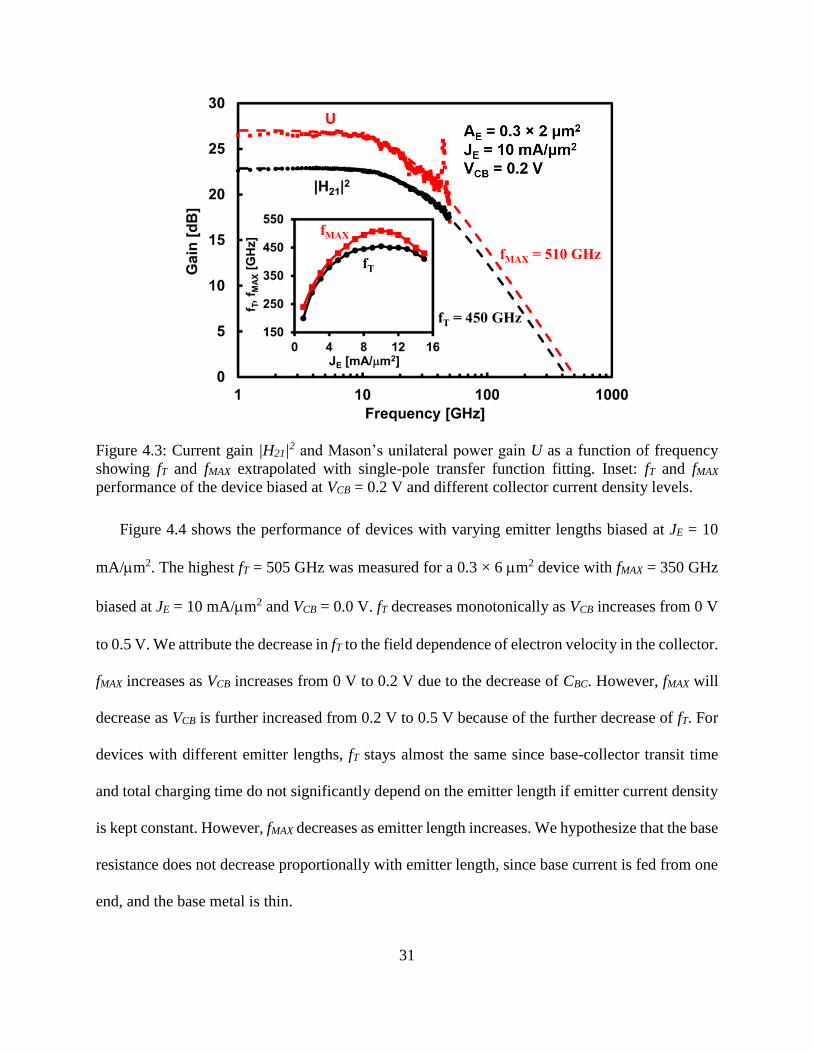
Figure 4.4 shows the performance of devices with varying emitter lengths biased at JE = 10
mA/m2. The highest fT = 505 GHz was measured for a 0.3 × 6 m2 device with fMAX = 350 GHz
biased at JE = 10 mA/m2 and VCB = 0.0 V. fT decreases monotonically as VCB increases from 0 V
to 0.5 V. We attribute the decrease in fT to the field dependence of electron velocity in the collector.
fMAX increases as VCB increases from 0 V to 0.2 V due to the decrease of CBC. However, fMAX will
decrease as VCB is further increased from 0.2 V to 0.5 V because of the further decrease of fT. For
devices with different emitter lengths, fT stays almost the same since base-collector transit time
and total charging time do not significantly depend on the emitter length if emitter current density
is kept constant. However, fMAX decreases as emitter length increases. We hypothesize that the base
resistance does not decrease proportionally with emitter length, since base current is fed from one
end, and the base metal is thin.
32
Figure 4.4: fT and fMAX performance of devices with different emitter lengths biased at JE = 10
mA/m2 and VCB = 0, 0.2, and 0.5 V.
4.3 Small-Signal Modeling and Parameter Extraction of Type-II InP DHBT
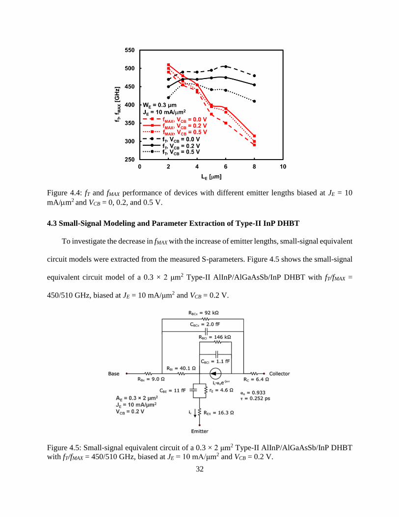
To investigate the decrease in fMAX with the increase of emitter lengths, small-signal equivalent
circuit models were extracted from the measured S-parameters. Figure 4.5 shows the small-signal
equivalent circuit model of a 0.3 × 2 μm2 Type-II AlInP/AlGaAsSb/InP DHBT with fT/fMAX =
450/510 GHz, biased at JE = 10 mA/μm2 and VCB = 0.2 V.
Figure 4.5: Small-signal equivalent circuit of a 0.3 × 2 μm2 Type-II AlInP/AlGaAsSb/InP DHBT
with fT/fMAX = 450/510 GHz, biased at JE = 10 mA/μm2 and VCB = 0.2 V.
33
The total emitter resistance REx+rE could be extracted from the measured Z-parameters using
Equation (4.1) [37, 38]. Here rE = nkT/IC is the emitter dynamic resistance, and Z is the Z-
parameters of the device, which could be transformed from the measured S-parameters using
Equations (4.2-4.5).
𝑅𝐸𝑥 + 𝑟𝐸 = 𝑟𝑒𝑎𝑙[𝑍12] (4.1)
𝑍11 =(1+𝑆11)(1−𝑆22)+𝑆12𝑆21
∆5 (4.2)
𝑍12 =2𝑆12
∆5 (4.3)
𝑍21 =2𝑆21
∆5 (4.4)
𝑍22 =(1−𝑆11)(1+𝑆22)+𝑆12𝑆21
∆5 (4.5)
∆5= (1 − 𝑆11)(1 − 𝑆22) − 𝑆12𝑆21 (4.6)
From Equation (4.1), we can see that the total emitter resistance of the device is a linear function
of the inverse of the total collector current. So, we can plot the total emitter resistance as a function
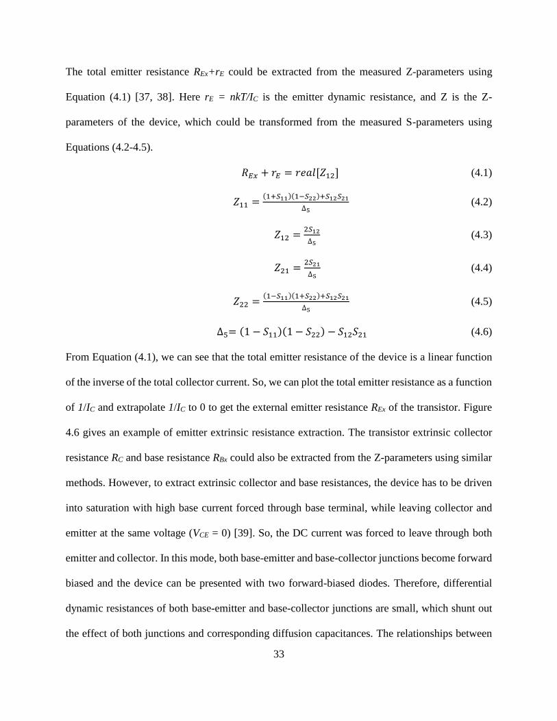
of 1/IC and extrapolate 1/IC to 0 to get the external emitter resistance REx of the transistor. Figure
4.6 gives an example of emitter extrinsic resistance extraction. The transistor extrinsic collector
resistance RC and base resistance RBx could also be extracted from the Z-parameters using similar
methods. However, to extract extrinsic collector and base resistances, the device has to be driven
into saturation with high base current forced through base terminal, while leaving collector and
emitter at the same voltage (VCE = 0) [39]. So, the DC current was forced to leave through both
emitter and collector. In this mode, both base-emitter and base-collector junctions become forward
biased and the device can be presented with two forward-biased diodes. Therefore, differential
dynamic resistances of both base-emitter and base-collector junctions are small, which shunt out
the effect of both junctions and corresponding diffusion capacitances. The relationships between
34
extrinsic collector and base resistances and Z-parameters are shown in the Equations (4.7-4.8).
𝑅𝐶 +𝑛𝐶𝑘𝑇
𝐼𝐵= 𝑟𝑒𝑎𝑙(𝑍22 − 𝑍21) (4.7)
𝑅𝐵𝑥 +𝑛𝐵𝑘𝑇
𝐼𝐵= 𝑟𝑒𝑎𝑙(𝑍11 − 𝑍12) (4.8)
So, we can extract RC and RBx by extrapolating 1/IB to zero.
Figure 4.6: Extraction of emitter resistance.
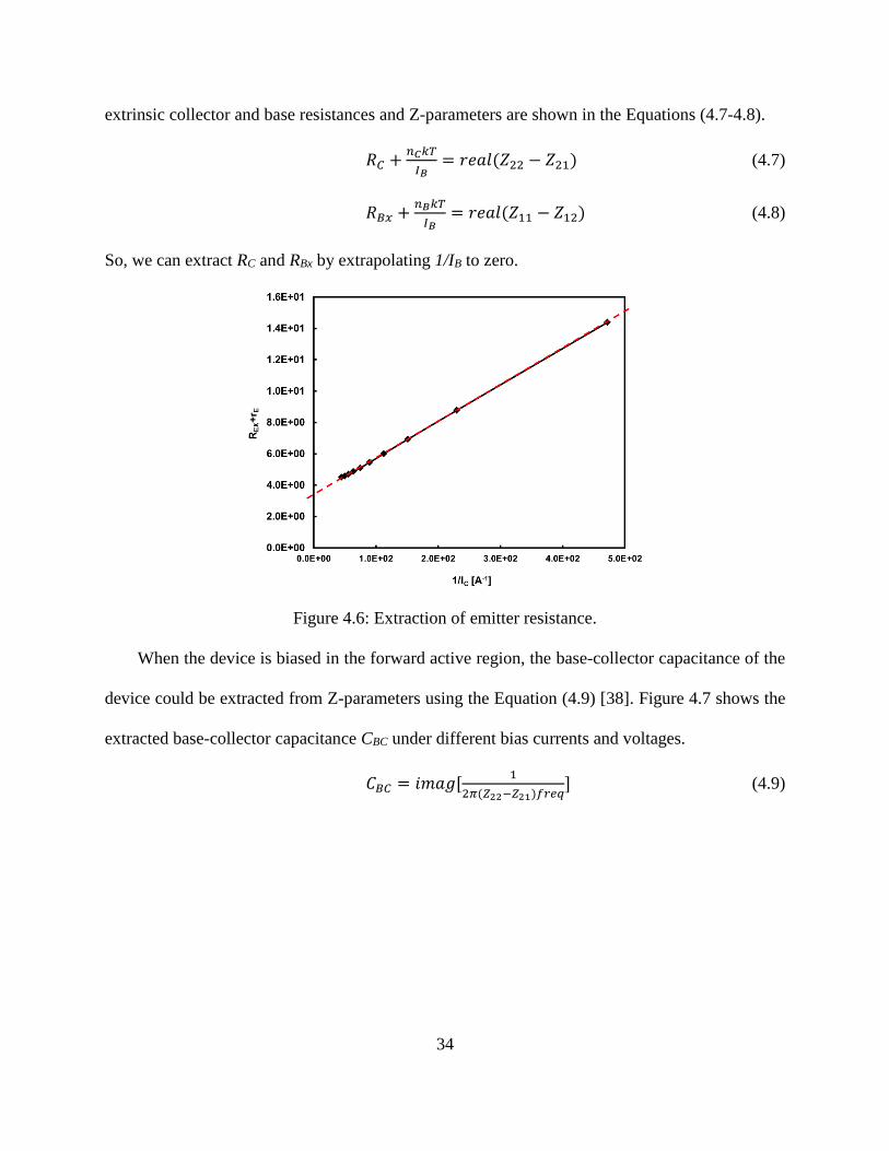
When the device is biased in the forward active region, the base-collector capacitance of the
device could be extracted from Z-parameters using the Equation (4.9) [38]. Figure 4.7 shows the
extracted base-collector capacitance CBC under different bias currents and voltages.
𝐶𝐵𝐶 = 𝑖𝑚𝑎𝑔[1
2𝜋(𝑍22−𝑍21)𝑓𝑟𝑒𝑞] (4.9)
35
Figure 4.7: The base-collector capacitance of a Type-II InP DHBT.
It is shown that when the reverse bias voltage of the base-collector junction VCB is increased, the
capacitance will decrease as a result of increased depletion width. In addition, as collector current
increases, the capacitance will first drop, but it will increase after collector current reaches a certain
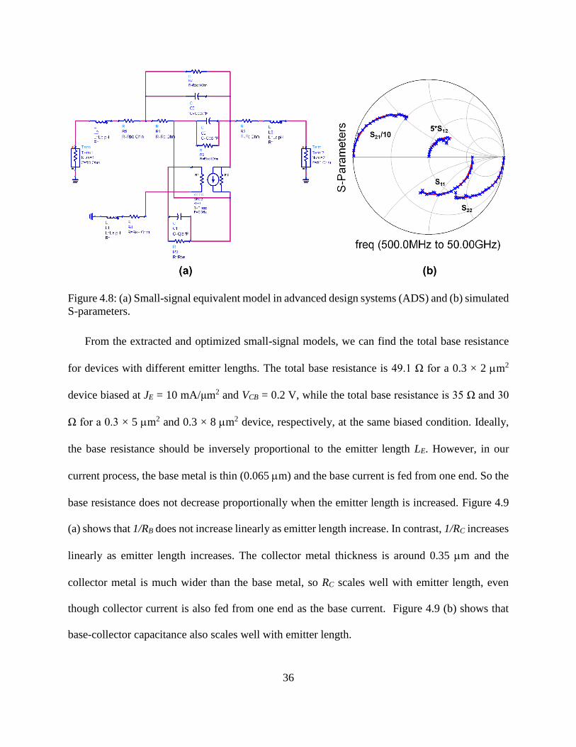
level. After the extraction of resistances and capacitance, a small-signal equivalent circuit model
could be constructed in ADS, and S-parameters could be simulated using this model. The extracted
small-signal circuit model parameters could be further optimized to fit the simulated S-parameters
with the measured S-parameters. Figure 4.8 shows the small-signal equivalent circuit model in
ADS, and simulated S-parameters fit well with measured S-parameters.
36
Figure 4.8: (a) Small-signal equivalent model in advanced design systems (ADS) and (b) simulated
S-parameters.
From the extracted and optimized small-signal models, we can find the total base resistance
for devices with different emitter lengths. The total base resistance is 49.1 Ω for a 0.3 × 2 m2
device biased at JE = 10 mA/μm2 and VCB = 0.2 V, while the total base resistance is 35 Ω and 30
Ω for a 0.3 × 5 m2 and 0.3 × 8 m2 device, respectively, at the same biased condition. Ideally,
the base resistance should be inversely proportional to the emitter length LE. However, in our
current process, the base metal is thin (0.065 m) and the base current is fed from one end. So the
base resistance does not decrease proportionally when the emitter length is increased. Figure 4.9
(a) shows that 1/RB does not increase linearly as emitter length increase. In contrast, 1/RC increases
linearly as emitter length increases. The collector metal thickness is around 0.35 m and the
collector metal is much wider than the base metal, so RC scales well with emitter length, even
though collector current is also fed from one end as the base current. Figure 4.9 (b) shows that
base-collector capacitance also scales well with emitter length.
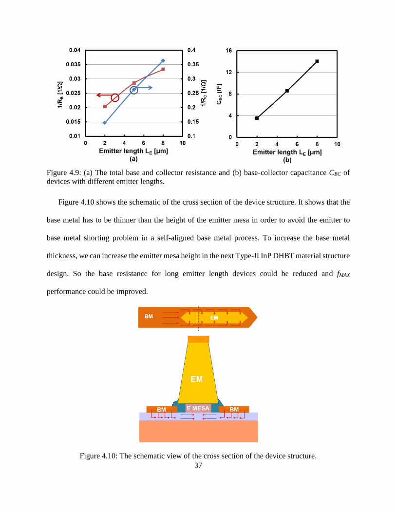
37
Figure 4.9: (a) The total base and collector resistance and (b) base-collector capacitance CBC of
devices with different emitter lengths.
Figure 4.10 shows the schematic of the cross section of the device structure. It shows that the
base metal has to be thinner than the height of the emitter mesa in order to avoid the emitter to
base metal shorting problem in a self-aligned base metal process. To increase the base metal
thickness, we can increase the emitter mesa height in the next Type-II InP DHBT material structure
design. So the base resistance for long emitter length devices could be reduced and fMAX
performance could be improved.
Figure 4.10: The schematic view of the cross section of the device structure.

38
4.4 Graded AlGaAsSb Base Type-II InP DHBT Transit Time Analysis
Time delay analysis was performed in order to test the hypothesis that the DHBT with AlxGa1-
xAsySb1-y base provides a higher built-in quasi-electric field and reduces base transit time compared
to DHBT with a GaxAs1-xSb base. As shown in Equation (1.1), the total delay time of a DHBT
consists of base and collector transit time 𝜏𝐵 , 𝜏𝐶 , emitter charging time 𝑛𝑘𝑇
𝑞𝐼𝐶𝐶𝐽𝐸 , and collector
charging time (𝑅𝐶 + 𝑅𝐸𝑥 +𝑛𝑘𝑇
𝑞𝐼𝐶)𝐶𝐵𝐶. To extract the base and collector transit time, the total delay
time τtotal was plotted as a function of 1/IC, and extrapolated to 1/IC = 0 to get 𝜏𝐵 + 𝜏𝐶 + (𝑅𝐶 +
𝑅𝐸𝑥)𝐶𝐵𝐶. Figure 4.11 shows the total delay time of a device as a function of 1/IC. The extracted
𝜏𝐵 + 𝜏𝐶 + (𝑅𝐶 + 𝑅𝐸𝑥)𝐶𝐵𝐶 is around 265 fs. Then, the (𝑅𝐶 + 𝑅𝐸𝑥)𝐶𝐵𝐶 term is subtracted using the
extracted values of RC, REx, and CBC from small-signal equivalent circuit model. For the Type-II
AlInP/AlGaAsSb/InP DHBT with a 20 nm graded AlGaAsSb base (Eg ≈ 135 meV) and 120 nm
InP collector, 𝜏𝐵 + 𝜏𝐶 is around 191 fs. In comparison, for a Type-I/II AlInP/GaAsSb/InP DHBT
with a 17 nm graded base (Eg ≈ 60 meV) and 100 nm InP collector, 𝜏𝐵 + 𝜏𝐶 is 196 fs [16].
Assuming the same average collector velocity of 3.76 × 107 cm/s for both devices, the graded
AlxGa1-xAsySb1-y base has 𝜏𝐵 = 31 fs, while the graded GaAsSb base has 𝜏𝐵 = 67 fs. Thus, AlxGa1-
xAsySb1-y with larger base energy grading can provide a significant reduction in the base transit
time, which provides high speed for both fT and fMAX.
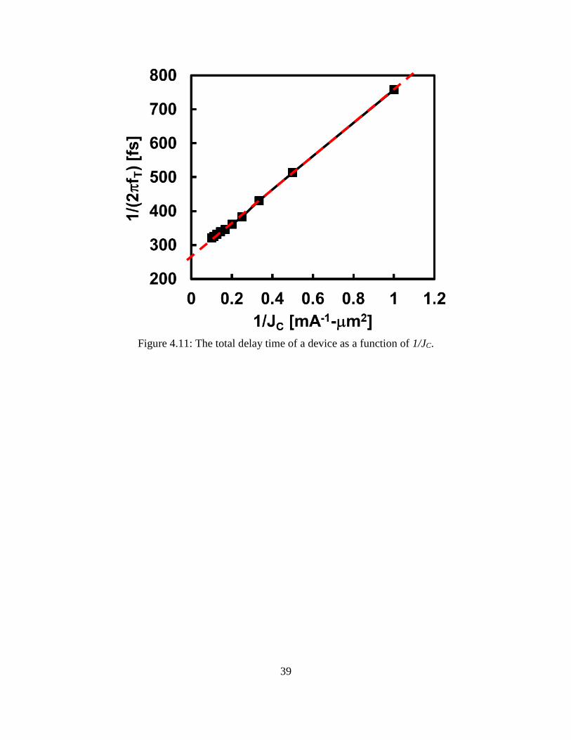
39
Figure 4.11: The total delay time of a device as a function of 1/JC.
40
5 DOPING-GRADED BASE TYPE-II GaAsSb/InP DHBT
5.1 Doping-Graded Base Type-II GaAsSb/InP DHBT
Although composition-graded GaAsSb, InGaAsSb, and AlGaAsSb base Type-II DHBTs have
reported good RF performance, the doping concentration is hard to control during the material
growth. In 2011, a Type-II DHBT with a doping-graded GaAsSb base was first reported with
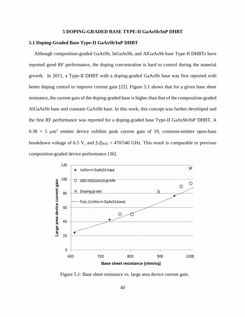
better doping control to improve current gain [22]. Figure 5.1 shows that for a given base sheet
resistance, the current gain of the doping-graded base is higher than that of the composition-graded
AlGaAsSb base and constant GaAsSb base. In this work, this concept was further developed and
the first RF performance was reported for a doping-graded base Type-II GaAsSb/InP DHBT. A
0.38 × 5 m2 emitter device exhibits peak current gain of 19, common-emitter open-base
breakdown voltage of 6.5 V, and fT/fMAX = 470/540 GHz. This result is comparable to previous
composition-graded device performance [36].
Figure 5.1: Base sheet resistance vs. large area device current gain.
41
The epitaxial structure for this work was grown on a 3-inch semi-insulating InP substrate by
molecular beam epitaxy (MBE). The 120 nm InP collector is lightly doped with silicon to 2 × 10¹⁶
cm-3. The base is formed by a 20 nm constant-composition GaAs0.5Sb0.5 with carbon doping, which
is graded to introduce an electric field in the base. The doping is linearly graded from 1.7 × 10²⁰
cm-3 on the emitter side to 8.2 × 1019 cm-3 on the collector side. The conduction band energy
difference across the doping-graded base is 74 meV. The base sheet resistance is 850 Ω/sq
determined from TLM measurement. The emitter consists of a 17.5 nm AlxIn1-xP layer linearly
graded from x = 0.1 on the base side to x = 0 on the emitter contact side, and a 20 nm InP layer,
both silicon doped at 4.0 × 1017 cm-3. The emitter contact consists of a 10 nm In0.53Ga0.47As layer,
and a 35 nm InxGa1-xAs layer graded from x = 0.53 to 1, both silicon doped at 5 × 1019 cm-3. The
detailed epilayer structure is shown in Table 5.1.
Table 5.1. Layer structure of the Type-II GaAsSb/InP DHBT.
Figure 5.2 shows the energy band diagram under equilibrium, which was simulated using
technology computer aided design (TCAD). Note the energy band slope formed in the base due to
graded doping. Devices with 0.38 m emitter width were fabricated using a triple-mesa wet-
42
etching process with metal contacts defined by a JEOL JBX-6000FS electron beam lithography
system [36]. An air-bridge was used to isolate the active device from the capacitances of the base
post metal. The device was planarized with BCB and etched back to make final top metal contact.
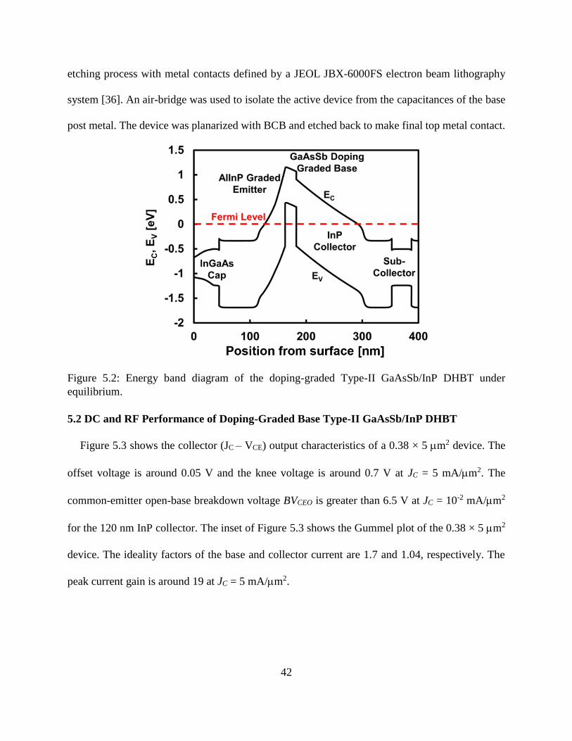
Figure 5.2: Energy band diagram of the doping-graded Type-II GaAsSb/InP DHBT under
equilibrium.
5.2 DC and RF Performance of Doping-Graded Base Type-II GaAsSb/InP DHBT
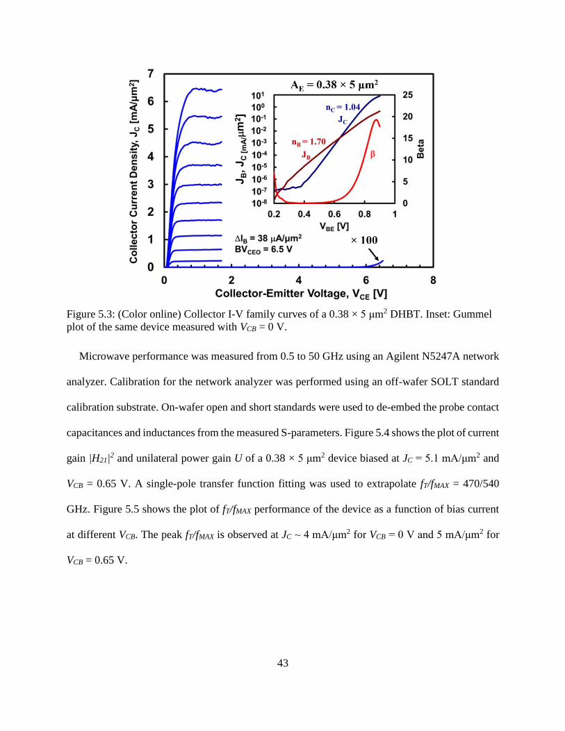
Figure 5.3 shows the collector (JC – VCE) output characteristics of a 0.38 × 5 m2 device. The
offset voltage is around 0.05 V and the knee voltage is around 0.7 V at JC = 5 mA/m2. The
common-emitter open-base breakdown voltage BVCEO is greater than 6.5 V at JC = 10-2 mA/m2
for the 120 nm InP collector. The inset of Figure 5.3 shows the Gummel plot of the 0.38 × 5 m2
device. The ideality factors of the base and collector current are 1.7 and 1.04, respectively. The
peak current gain is around 19 at JC = 5 mA/m2.
43
Figure 5.3: (Color online) Collector I-V family curves of a 0.38 × 5 μm2 DHBT. Inset: Gummel
plot of the same device measured with VCB = 0 V.
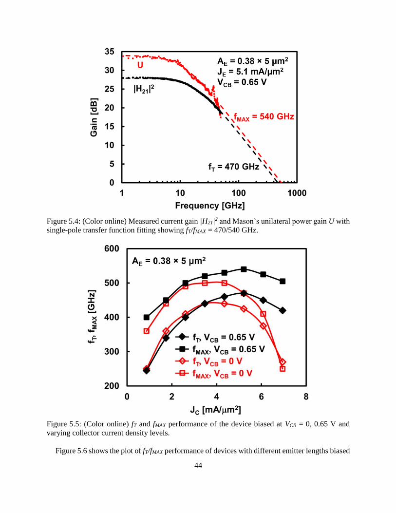
Microwave performance was measured from 0.5 to 50 GHz using an Agilent N5247A network
analyzer. Calibration for the network analyzer was performed using an off-wafer SOLT standard
calibration substrate. On-wafer open and short standards were used to de-embed the probe contact
capacitances and inductances from the measured S-parameters. Figure 5.4 shows the plot of current
gain |H21|2 and unilateral power gain U of a 0.38 × 5 μm2 device biased at JC = 5.1 mA/μm2 and
VCB = 0.65 V. A single-pole transfer function fitting was used to extrapolate fT/fMAX = 470/540
GHz. Figure 5.5 shows the plot of fT/fMAX performance of the device as a function of bias current
at different VCB. The peak fT/fMAX is observed at JC ~ 4 mA/μm2 for VCB = 0 V and 5 mA/μm2 for
VCB = 0.65 V.
44
Figure 5.4: (Color online) Measured current gain |H21|2 and Mason’s unilateral power gain U with
single-pole transfer function fitting showing fT/fMAX = 470/540 GHz.
Figure 5.5: (Color online) fT and fMAX performance of the device biased at VCB = 0, 0.65 V and
varying collector current density levels.
Figure 5.6 shows the plot of fT/fMAX performance of devices with different emitter lengths biased
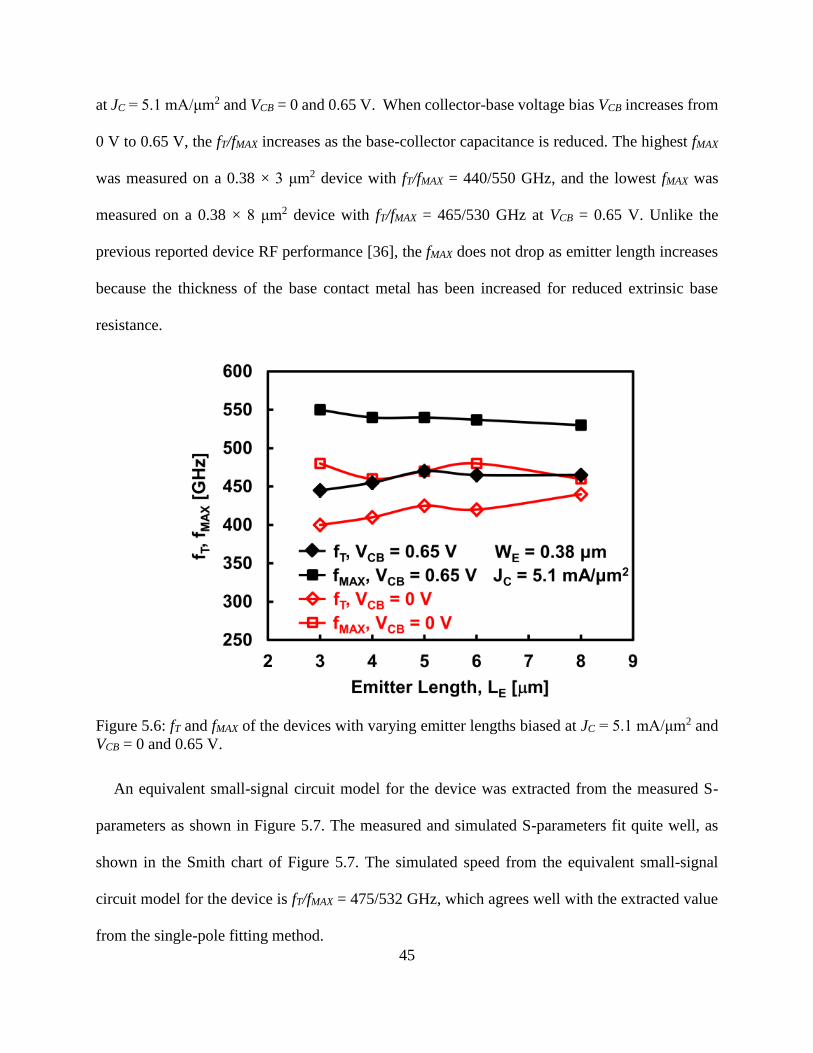
45
at JC = 5.1 mA/μm2 and VCB = 0 and 0.65 V. When collector-base voltage bias VCB increases from
0 V to 0.65 V, the fT/fMAX increases as the base-collector capacitance is reduced. The highest fMAX
was measured on a 0.38 × 3 μm2 device with fT/fMAX = 440/550 GHz, and the lowest fMAX was
measured on a 0.38 × 8 μm2 device with fT/fMAX = 465/530 GHz at VCB = 0.65 V. Unlike the
previous reported device RF performance [36], the fMAX does not drop as emitter length increases
because the thickness of the base contact metal has been increased for reduced extrinsic base
resistance.
Figure 5.6: fT and fMAX of the devices with varying emitter lengths biased at JC = 5.1 mA/μm2 and
VCB = 0 and 0.65 V.
An equivalent small-signal circuit model for the device was extracted from the measured S-
parameters as shown in Figure 5.7. The measured and simulated S-parameters fit quite well, as
shown in the Smith chart of Figure 5.7. The simulated speed from the equivalent small-signal
circuit model for the device is fT/fMAX = 475/532 GHz, which agrees well with the extracted value
from the single-pole fitting method.
46
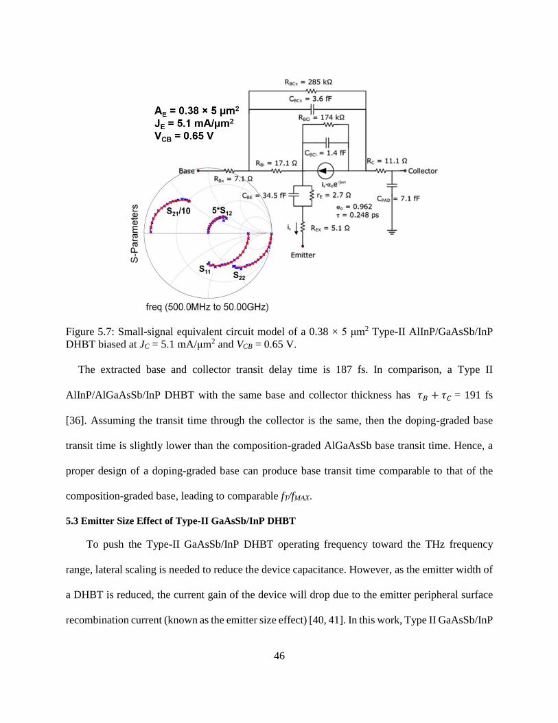
Figure 5.7: Small-signal equivalent circuit model of a 0.38 × 5 μm2 Type-II AlInP/GaAsSb/InP
DHBT biased at JC = 5.1 mA/μm2 and VCB = 0.65 V.
The extracted base and collector transit delay time is 187 fs. In comparison, a Type II
AlInP/AlGaAsSb/InP DHBT with the same base and collector thickness has 𝜏𝐵 + 𝜏𝐶 = 191 fs
[36]. Assuming the transit time through the collector is the same, then the doping-graded base
transit time is slightly lower than the composition-graded AlGaAsSb base transit time. Hence, a
proper design of a doping-graded base can produce base transit time comparable to that of the
composition-graded base, leading to comparable fT/fMAX.
5.3 Emitter Size Effect of Type-II GaAsSb/InP DHBT
To push the Type-II GaAsSb/InP DHBT operating frequency toward the THz frequency
range, lateral scaling is needed to reduce the device capacitance. However, as the emitter width of
a DHBT is reduced, the current gain of the device will drop due to the emitter peripheral surface
recombination current (known as the emitter size effect) [40, 41]. In this work, Type II GaAsSb/InP
47
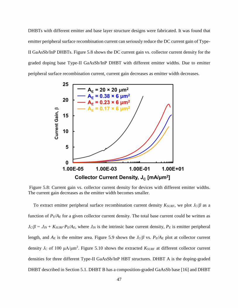
DHBTs with different emitter and base layer structure designs were fabricated. It was found that
emitter peripheral surface recombination current can seriously reduce the DC current gain of Type-
II GaAsSb/InP DHBTs. Figure 5.8 shows the DC current gain vs. collector current density for the
graded doping base Type-II GaAsSb/InP DHBT with different emitter widths. Due to emitter
peripheral surface recombination current, current gain decreases as emitter width decreases.
Figure 5.8: Current gain vs. collector current density for devices with different emitter widths.
The current gain decreases as the emitter width becomes smaller.
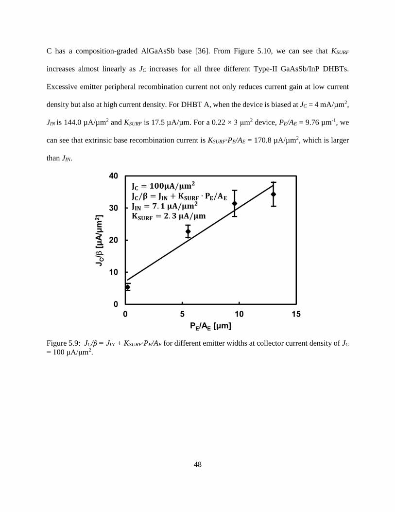
To extract emitter peripheral surface recombination current density KSURF, we plot JC/β as a
function of PE/AE for a given collector current density. The total base current could be written as
JC/β = JIN + KSURF·PE/AE, where JIN is the intrinsic base current density, PE is emitter peripheral
length, and AE is the emitter area. Figure 5.9 shows the JC/β vs. PE/AE plot at collector current
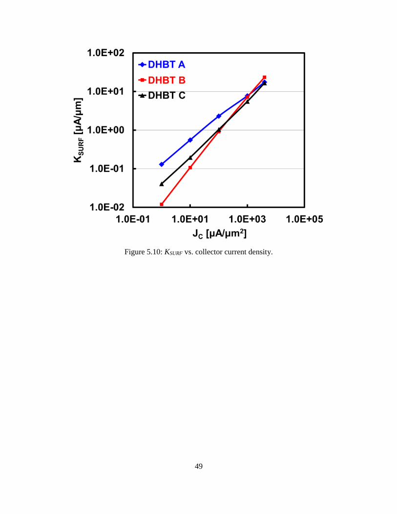
density JC of 100 μA/μm2. Figure 5.10 shows the extracted KSURF at different collector current
densities for three different Type-II GaAsSb/InP HBT structures. DHBT A is the doping-graded
DHBT described in Section 5.1. DHBT B has a composition-graded GaAsSb base [16] and DHBT
48
C has a composition-graded AlGaAsSb base [36]. From Figure 5.10, we can see that KSURF
increases almost linearly as JC increases for all three different Type-II GaAsSb/InP DHBTs.
Excessive emitter peripheral recombination current not only reduces current gain at low current
density but also at high current density. For DHBT A, when the device is biased at JC = 4 mA/µm2,
JIN is 144.0 µA/µm2 and KSURF is 17.5 µA/µm. For a 0.22 × 3 μm2 device, PE/AE = 9.76 µm-1, we
can see that extrinsic base recombination current is KSURF·PE/AE = 170.8 µA/µm2, which is larger
than JIN.
Figure 5.9: JC/β = JIN + KSURF·PE/AE for different emitter widths at collector current density of JC
= 100 μA/μm2.
49
Figure 5.10: KSURF vs. collector current density.
50
6 DOPING-GRADED BASE TYPE-II GaAsSb/InP DHBT WITH AN EMITTER LEDGE
6.1 Emitter Ledge Process Development
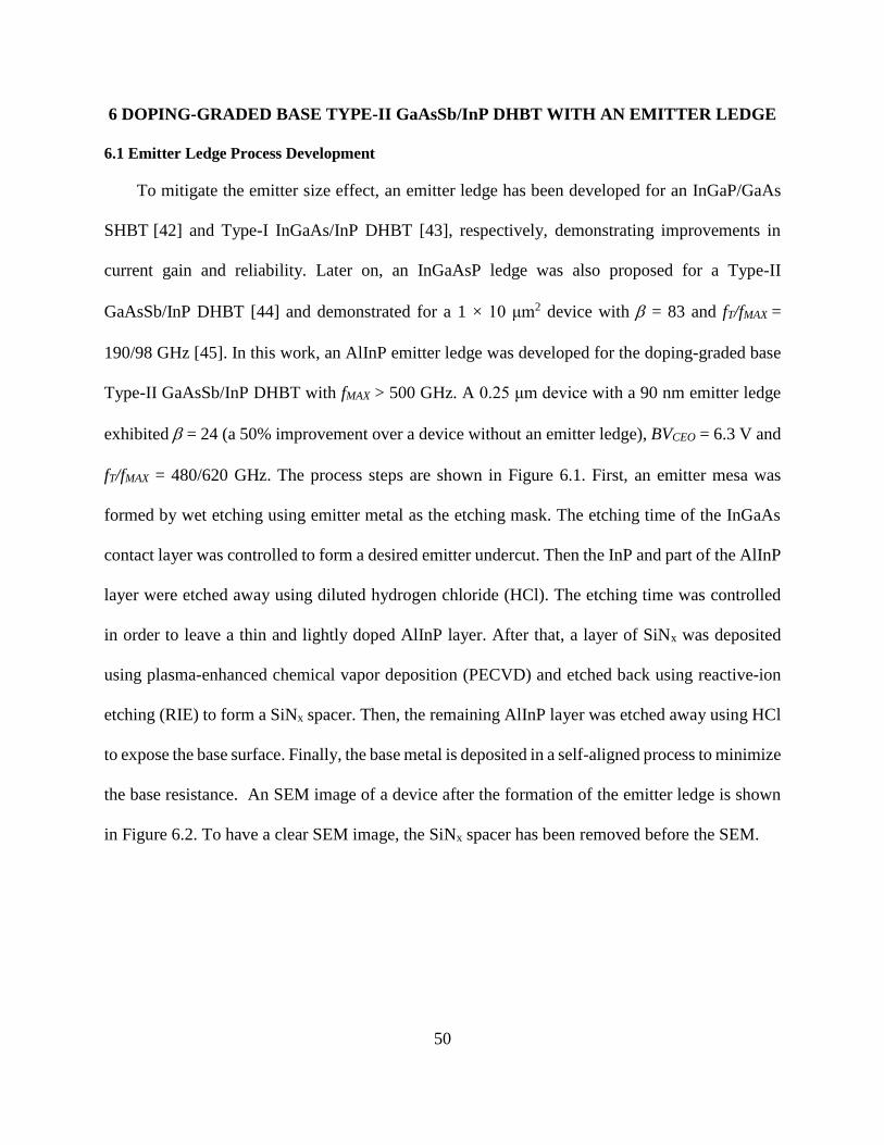
To mitigate the emitter size effect, an emitter ledge has been developed for an InGaP/GaAs
SHBT [42] and Type-I InGaAs/InP DHBT [43], respectively, demonstrating improvements in
current gain and reliability. Later on, an InGaAsP ledge was also proposed for a Type-II
GaAsSb/InP DHBT [44] and demonstrated for a 1 × 10 μm2 device with = 83 and fT/fMAX =
190/98 GHz [45]. In this work, an AlInP emitter ledge was developed for the doping-graded base
Type-II GaAsSb/InP DHBT with fMAX > 500 GHz. A 0.25 μm device with a 90 nm emitter ledge
exhibited = 24 (a 50% improvement over a device without an emitter ledge), BVCEO = 6.3 V and
fT/fMAX = 480/620 GHz. The process steps are shown in Figure 6.1. First, an emitter mesa was
formed by wet etching using emitter metal as the etching mask. The etching time of the InGaAs
contact layer was controlled to form a desired emitter undercut. Then the InP and part of the AlInP
layer were etched away using diluted hydrogen chloride (HCl). The etching time was controlled
in order to leave a thin and lightly doped AlInP layer. After that, a layer of SiNx was deposited
using plasma-enhanced chemical vapor deposition (PECVD) and etched back using reactive-ion
etching (RIE) to form a SiNx spacer. Then, the remaining AlInP layer was etched away using HCl
to expose the base surface. Finally, the base metal is deposited in a self-aligned process to minimize
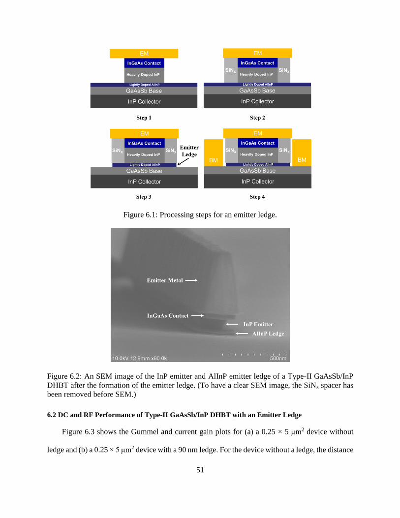
the base resistance. An SEM image of a device after the formation of the emitter ledge is shown
in Figure 6.2. To have a clear SEM image, the SiNx spacer has been removed before the SEM.
51
Figure 6.1: Processing steps for an emitter ledge.
Figure 6.2: An SEM image of the InP emitter and AlInP emitter ledge of a Type-II GaAsSb/InP
DHBT after the formation of the emitter ledge. (To have a clear SEM image, the SiNx spacer has
been removed before SEM.)
6.2 DC and RF Performance of Type-II GaAsSb/InP DHBT with an Emitter Ledge
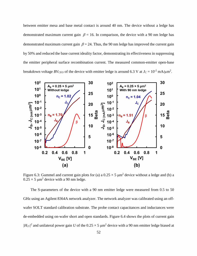
Figure 6.3 shows the Gummel and current gain plots for (a) a 0.25 × 5 μm2 device without
ledge and (b) a 0.25 × 5 μm2 device with a 90 nm ledge. For the device without a ledge, the distance
52
between emitter mesa and base metal contact is around 40 nm. The device without a ledge has
demonstrated maximum current gain = 16. In comparison, the device with a 90 nm ledge has
demonstrated maximum current gain = 24. Thus, the 90 nm ledge has improved the current gain
by 50% and reduced the base current ideality factor, demonstrating its effectiveness in suppressing
the emitter peripheral surface recombination current. The measured common-emitter open-base
breakdown voltage BVCEO of the device with emitter ledge is around 6.3 V at JC = 10-2 mA/m2.
Figure 6.3: Gummel and current gain plots for (a) a 0.25 × 5 μm2 device without a ledge and (b) a
0.25 × 5 μm2 device with a 90 nm ledge.
The S-parameters of the device with a 90 nm emitter ledge were measured from 0.5 to 50
GHz using an Agilent 8364A network analyzer. The network analyzer was calibrated using an off-
wafer SOLT standard calibration substrate. The probe contact capacitances and inductances were
de-embedded using on-wafer short and open standards. Figure 6.4 shows the plots of current gain
|H21|2 and unilateral power gain U of the 0.25 × 5 μm2 device with a 90 nm emitter ledge biased at
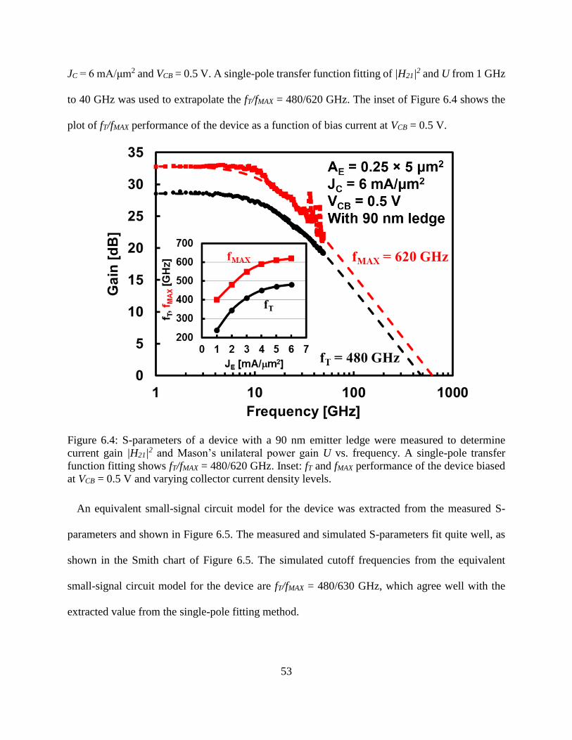
53
JC = 6 mA/μm2 and VCB = 0.5 V. A single-pole transfer function fitting of |H21|2 and U from 1 GHz
to 40 GHz was used to extrapolate the fT/fMAX = 480/620 GHz. The inset of Figure 6.4 shows the
plot of fT/fMAX performance of the device as a function of bias current at VCB = 0.5 V.
Figure 6.4: S-parameters of a device with a 90 nm emitter ledge were measured to determine
current gain |H21|2 and Mason’s unilateral power gain U vs. frequency. A single-pole transfer
function fitting shows fT/fMAX = 480/620 GHz. Inset: fT and fMAX performance of the device biased
at VCB = 0.5 V and varying collector current density levels.
An equivalent small-signal circuit model for the device was extracted from the measured S-
parameters and shown in Figure 6.5. The measured and simulated S-parameters fit quite well, as
shown in the Smith chart of Figure 6.5. The simulated cutoff frequencies from the equivalent
small-signal circuit model for the device are fT/fMAX = 480/630 GHz, which agree well with the
extracted value from the single-pole fitting method.
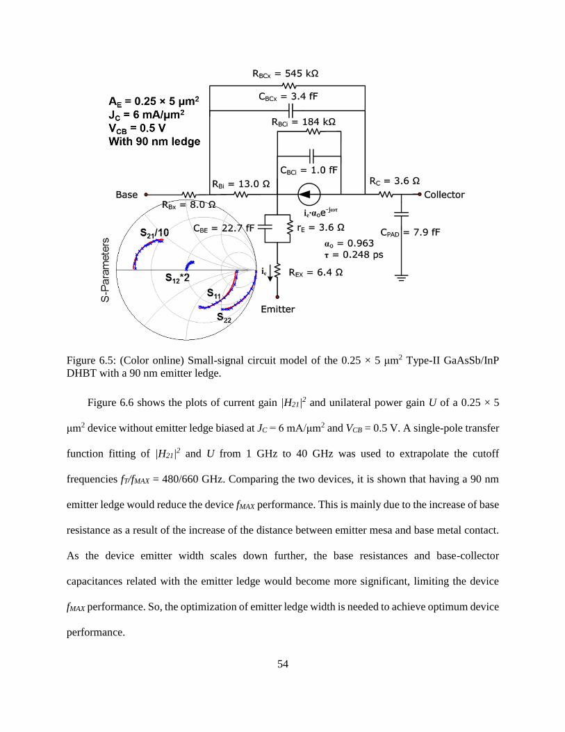
54
Figure 6.5: (Color online) Small-signal circuit model of the 0.25 × 5 μm2 Type-II GaAsSb/InP
DHBT with a 90 nm emitter ledge.
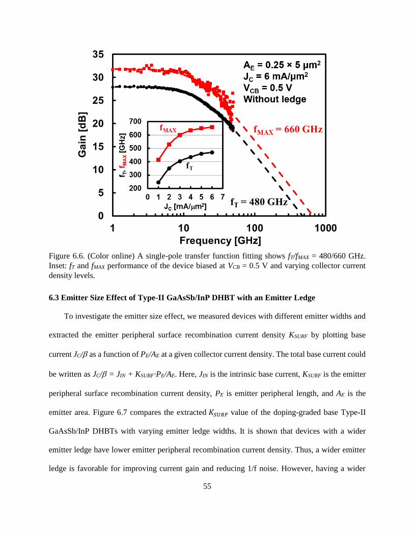
Figure 6.6 shows the plots of current gain |H21|2 and unilateral power gain U of a 0.25 × 5
μm2 device without emitter ledge biased at JC = 6 mA/μm2 and VCB = 0.5 V. A single-pole transfer
function fitting of |H21|2 and U from 1 GHz to 40 GHz was used to extrapolate the cutoff
frequencies fT/fMAX = 480/660 GHz. Comparing the two devices, it is shown that having a 90 nm
emitter ledge would reduce the device fMAX performance. This is mainly due to the increase of base
resistance as a result of the increase of the distance between emitter mesa and base metal contact.
As the device emitter width scales down further, the base resistances and base-collector
capacitances related with the emitter ledge would become more significant, limiting the device
fMAX performance. So, the optimization of emitter ledge width is needed to achieve optimum device
performance.
55
Figure 6.6. (Color online) A single-pole transfer function fitting shows fT/fMAX = 480/660 GHz.
Inset: fT and fMAX performance of the device biased at VCB = 0.5 V and varying collector current
density levels.
6.3 Emitter Size Effect of Type-II GaAsSb/InP DHBT with an Emitter Ledge
To investigate the emitter size effect, we measured devices with different emitter widths and
extracted the emitter peripheral surface recombination current density KSURF by plotting base
current JC/ as a function of PE/AE at a given collector current density. The total base current could
be written as JC/ = JIN + KSURF·PE/AE. Here, JIN is the intrinsic base current, KSURF is the emitter
peripheral surface recombination current density, PE is emitter peripheral length, and AE is the
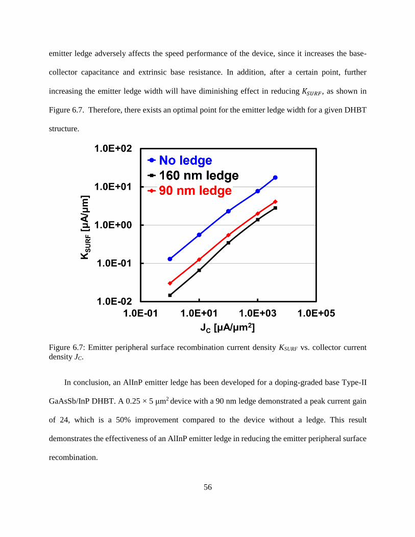
emitter area. Figure 6.7 compares the extracted 𝐾𝑆𝑈𝑅𝐹 value of the doping-graded base Type-II
GaAsSb/InP DHBTs with varying emitter ledge widths. It is shown that devices with a wider
emitter ledge have lower emitter peripheral recombination current density. Thus, a wider emitter
ledge is favorable for improving current gain and reducing 1/f noise. However, having a wider
56
emitter ledge adversely affects the speed performance of the device, since it increases the base-
collector capacitance and extrinsic base resistance. In addition, after a certain point, further
increasing the emitter ledge width will have diminishing effect in reducing 𝐾𝑆𝑈𝑅𝐹, as shown in
Figure 6.7. Therefore, there exists an optimal point for the emitter ledge width for a given DHBT
structure.
Figure 6.7: Emitter peripheral surface recombination current density KSURF vs. collector current
density JC.
In conclusion, an AlInP emitter ledge has been developed for a doping-graded base Type-II
GaAsSb/InP DHBT. A 0.25 × 5 μm2 device with a 90 nm ledge demonstrated a peak current gain
of 24, which is a 50% improvement compared to the device without a ledge. This result
demonstrates the effectiveness of an AlInP emitter ledge in reducing the emitter peripheral surface
recombination.
57
7 CONCLUSION
The DC, RF, and nonlinearity performance of a Type-I/II AlInP/GaAsSb/InP DHBT has been
characterized and compared with that of a foundry-provided Type-I InP/InGaAs/InP DHBT. It was
found that the Type-I InP/InGaAs/InP DHBT has higher knee voltage and larger gain compression
than does the Type-I/II AlInP/GaAsSb/InP DHBT at high collector current density levels. The
Type-I InP/InGaAs/InP DHBT also shows larger fT drop and lower OIP3 (worse nonlinearity) at
high collector current density levels than does the Type-II AlInP/GaAsSb/InP DHBT.
Hydrodynamic device simulation shows that as collector current density increases, the collector
transition layer and collector layer of the Type-I InP/InGaAs/InP DHBT will become flatter,
leading to base push-out and excessive charge accumulation in the base. So it could result in DC
and RF gain compression, increased base transit time, fT fall-off, and reduction of OIP3.
A Type-II AlInP/AlGaAsSb/InP DHBT has been designed, grown, and fabricated. The DHBT
structure demonstrates peak current gain = 20 for 0.3 m devices and breakdown voltage BVCEO
> 5.0 V. A 0.3 × 2 m2 device also shows fMAX = 510 GHz with fT = 450 GHz at JE = 10 mA/μm2
and VCB = 0.2 V. Small-signal modeling and delay time analysis shows that the graded AlGaAsSb
base can provide a larger energy gradient in the base than that of the GaAsSb base, leading to
reduced base transit time and higher fT/fMAX performance. It was found that the fMAX performance
of the Type-II AlInP/AlGaAsSb/InP DHBT decreases for devices with longer emitter length. The
fMAX performance drop is due to the fact that base resistance does not decrease proportionally with
emitter length, while base-collector capacitance increases proportionally with the emitter length.
The base resistance scaling problem arises because the base metal is thin (limited by the emitter
mesa height) and the base current is fed from one end of the device.
58
To improve the device fMAX performance, a doping-graded base Type-II AlInP/GaAsSb/InP
DHBT with higher emitter mesa was designed. For a given base sheet resistance, the current gain
of the doping-graded base is higher than that of composition-graded AlGaAsSb base and constant
GaAsSb base. For devices with increased base metal thickness, the fMAX does not drop as emitter
length increases due to the reduced extrinsic base resistance. An AlInP emitter ledge has also been
developed for the DHBT with a doping-graded base. Compared with devices without an emitter
ledge, devices with an AlInP emitter ledge have shown much lower emitter peripheral surface
recombination current density. So, an AlInP emitter ledge can effectively suppress the emitter size
effect and improve current gain. A 0.25 × 5 m2 device with a 90 nm AlInP emitter ledge has
demonstrated maximum current gain = 24, BVCEO = 6.3 V, and fT/fMAX = 480/620 GHz.
59
REFERENCES
[1] J. Bardeen and W. H. Brattain, “The transistor, a semiconductor triode,” Physics Review,
vol. 74, pp. 230-231, 1948.
[2] W. Shockley, “Theory of p-n junctions in semiconductors and p-n junction transistors,” Bell
System Technology Journal, vol. 28, pp. 435-489, 1949.
[3] W. Shockley, M. Sparks, and G. K. Teal, “p-n junction transistors,” Physical Review, vol.
83, no. 1, pp. 151-162, 1951.
[4] W. Shockley, “Circuit element utilizing semiconductive material.” United States of America
Patent 2,569,347, 26 June 1948.
[5] H. Kroemer, “Theory of a wide-gap emitter for transistors,” Proceedings of the Institute of
Radio Engineers, vol. 45, pp. 1535-1537, 1957.
[6] D. C. Streit, J. C. Cowles, K. W. Kobayashi, A. G. Aitken, T. R. Block, M. Wojotowicz, F.
Yamada, E. Kaneshiro, et al., “InP technology and applications,” in 10th Intern. Conf. on
Indium Phosphide and Related Materials, Tsukuba, Japan, 1998.
[7] T. S. Low, M. W. Dvorak, M. Farhoud, R. E. Yeats, M. Iwamoto, G. K. Essilfie, T. Engel,
B. Keppeler, J. S. C. Chang, J. Hadley, G. Patterson, F. Kellert, N. Moll, S. R. Bahl, C. P.
Hutchinson, E. Ehlers, et al., “GaAsSb DHBT IC technology for RF and microwave
instrumentation,” in IEEE Compound Semiconductor Integrated Circuit Symposium, Palm
Springs, CA, 2005.
[8] R. Driad, R. E. Makon, V. Hurm, F. Benkhelifa, R. Losch, J. Rosenzweig, and M.
Schlechtweg, “InP-based DHBT technology for high-speed mixed signal and digital
applications,” in IEEE Indium Phosphide & Related Materials, Newport Beach, CA, 2009.
[9] W. Liu, Handbook of III-V Heterojunction Bipolar Transistors, New York: Wiley-
Interscience, 1998.
[10] S. J. Mason, “Power gain in feedback amplifier,” Transactions of the Institute of Radio
Engineers, vol. CT-1, no. 2, pp. 20-25, 1954.
[11] K. Kurishima, “An analytic expression of fmax for HBTs,” IEEE Transactions on Electron
Devices, vol. 43, no. 12, pp. 2074-2079, 1996.
60
[12] W. Snodgrass, W. Hafez, N. Harff, and M. Feng, “Pseudomorphic InP/InGaAs
heterojunction bipolar transistors (PHBTs) experimentally demonstrating ft = 765 GHz at 25 oC increasing to ft = 845 GHz at −55 oC,” in International Electron Devices Meeting, San
Francisco, CA, 2006.
[13] M. Urteaga, R. Pierson, P. Rowell, V. Jain, E. Lobisser, and M. J. W. Rodwell, “130 nm InP
DHBTs with ft > 0.52 THz and fmax > 1.1 THz,” in Device Research Conference, Santa
Barbara, CA, 2011.
[14] K. Y. (Donald) Cheng, H. Xu, M. E. Stuenkel, E. W. Iverson, C. C. Liao, K. W. Yang, M.
Feng, and K. Y. (Norman) Cheng, “Base charge accumulation and push-out effects on
nonlinearity of Type-I InP/InGaAs/InP and Type-I/II AlInP/GaAsSb/InP double
heterojunction bipolar transistors,” Journal of Applied Physics, vol. 110, p. 113703, 2011.
[15] Y. Oda, H. Yokoyama, K. Kurishima, T. Kobayashi, N. Watanabe, and M. Uchida,
“Improvement of current gain of C-doped GaAsSb-base heterojunction bipolar transistors
by using an InAlP emitter,” Applied Physics Letters, vol. 87, p. 023503, 2005.
[16] K. Y. (Donald) Cheng, C. C. Liao, H. Xu, K. Y. (Norman) Cheng, and M. Feng, “Hot
electron injection effect on the microwave performance of Type-I/II AlInP/GaAsSb/InP
double heterojunction bipolar transistors,” Applied Physics Letters, vol. 98, no. 24, p.
242103, 2011.
[17] I. Vurgaftman, J. R. Meyer, and L. R. Ram-Mohan, “Band parameters for III-V compound
semiconductors and their alloys,” Journal of Applied Physics, vol. 89, no. 11, pp. 5815-5875,
2001.
[18] H. G. Liu, O. Ostinelli, Y. Zeng, and C. R. Bolognesi, “600 GHz InP/GaAsSb/InP DHBTs
grown by MOCVD with a Ga(As,Sb) graded-base and fT × BVCEO ≫ 2.5 THz-V at room
temperature,” in IEEE International Electron Devices Meeting, Washington DC, 2007.
[19] W. Snodgrass, B. R. Wu, W. Hafez, K. Y. Cheng, and M. Feng, “Graded base Type-II
InP/GaAsSb DHBT with fT = 475 GHz,” IEEE Electron Devices Letters, vol. 27, no. 2, pp.
84-86, 2006.
[20] Y. Oda, N. Watanabe, K. Kurishima, M. Uchida, and T. Kobayashi, “Effect of a
compositionally-graded GaAsSb-base in InAlP/GaAsSb/InP HBTs,” in Electronic Materials
Symposium, 2005.
[21] Y. Oda, K. Kurishima, N. Watanabe, M. Uchida, and T. Kobayashi, “High-current-gain
InAlP/AlGaAsSb/InP HBTs with a compositionally-graded AlGaAsSb base grown by
61
MOCVD,” in IEEE Indium Phosphide and Related Materials, Princeton, NJ, 2006, pp. 92-
95.
[22] B. R. Wu, M. W. Dvorak, P. Colbus, T. S. Low, and D. D' Avanzo, “High current gain of
doping-graded GaAsSb/InP DHBTs,” in IEEE Indium Phosphide and Related Materials,
Berlin, Germany, 2011, pp. 1-3.
[23] M. J. W. Rodwell, M. Urteaga, T. Mathew, D. Scott, D. Mensa, Q. Lee, J. Guthrie, Y. Betser,
S. C. Martin, R. P. Smith, S. Jaganathan, S. Krishnan, S. I. Long, R. Pullela, B. Agarwal, U.
Bhattacharya, L. Samoska, and M. Dahlstrom, “Submicron scaling of HBTs,” IEEE
Tansactions on Electron Devices, vol. 48, no. 11, pp. 2606-2624, 2001.
[24] C. T. Kirk, “A theory of transistor cutoff frequency (fT) falloff at high current densities,” IRE
Transactions on Electron Devices, vol. 9, no. 2, pp. 164-174, 1962.
[25] S. Tiwari, “A new effect at high currents in heterostructure bipolar transistors,” IEEE
Electron Devcie Letters, vol. 9, no. 3, pp. 142-144, 1988.
[26] W. Snodgrass, B. R. Wu, K. Y. Cheng and M. Feng, “Type-II GaAsSb/InP DHBT with
record fT = 670 GHz and simultaneous fT, fMAX > 400 GHz,” in IEEE International Electron
Devices Meeting, Washington DC, 2007.
[27] J. W. Lai, W. Hafez, and M. Feng, “Vertical scaling of Type I InP HBT With fT > 500 GHz,”
International Journal of High Speed Electronics and Systems, vol. 14, no. 3, pp. 625-631,
2004.
[28] R. Lövblom, R. Flückiger, M. Alexandrova, O. Ostinelli, and C. R. Bolognesi, “InP/GaAsSb
DHBTs with simultaneous fT/fMAX = 428/621 GHz,” IEEE Electron Device Letters, vol. 34,
no. 8, pp. 984-986, 2013.
[29] C. Nguyen, T. Liu, M. Chen, H. Sun, and D. Rensch, “AlInAs/GaInAs/InP double
heterojunction bipolar transistor with a novel base collector design for power applications,”
in IEEE International Electron Device Meeting, Washington D.C., 1995.
[30] Z. Griffith, E. Lind, M. J. W. Rodwell, X. M. Fang, D. Loubychev, Y. Wu, J. M. Fastenau,
and A. W. K. Liu, “Sub-300 nm InGaAs/InP Type-I DHBTs with a 150 nm collector, 30 nm
base demonstrating 755 GHz fMAX and 416 GHz fT,” in International Conference on Indium
Phosphide and Related Materials, Matsue, Japan, 2007.
[31] H. C. Poon, “Implication of transistor frequency dependence on intermodulation distortion,”
IEEE Transactions on Electron Devices, vol. ED-21, no. 1, pp. 110-112, 1974.
62
[32] M. Vaidyanathan, M. Iwamoto, L. E. Larson, P. S. Gudem, and P. M. Asbeck, “A theory of
high-frequency distortion in bipolar transistors,” IEEE Transactions on Microwave Theory
and Techniques, vol. 51, no. 2, pp. 448-461, 2003.
[33] Sentaurus Device User Guide Version E-2010.12, CA: Synopsys, 2010.
[34] H. Xu, E. W. Iverson, K. Y. (Donald) Cheng, and M. Feng, “Physical origins of nonlinearity
in InP double heterojunction bipolar transistors,” Applied Physics Letters, vol. 100, no.
113508, pp. 1-3, 2012.
[35] B. R. Wu, M. W. Dvorak, P. Colbus, T. S. Low, and D. D' Avanzo, “Performance
improvement of composition-graded AlGaAsSb/InP double heterojunction bipolar
transistors,” in International Conference on Indium Phosphide & Related Materials,
Newport Beach, CA, 2009.
[36] H. Xu, E. W. Iverson, C. C. Liao, K. Y. Cheng, and M. Feng, “Composition-graded
AlInP/AlGaAsSb/InP Type-II DHBTs with fT/fMAX = 450/510 GHz,” IEEE Electron Device
Letters, vol. 34, no. 1, pp. 33-35, 2013.
[37] M. Sotoodeh, L. Sozzi, A. Vinay, A. H. Khalid, Z. Hu, A. A. Rezazadeh, and R. Menozzi,
“Steeping toward standard methods of small-signal parameter extraction for HBTs,” IEEE
Transactions on Electron Devices, vol. 47, no. 6, pp. 1139-1151, 2000.
[38] M. W. Dvorak and C. R. Bolognesi, “On the accuracy of direct extraction of the
heterojunction-bipolar-transistor equivalent-circuit model parameters Cπ, CBC, and RE,”
IEEE Transactions on Microwave Theory and Techniques, vol. 51, no. 6, pp. 1640-1649,
2003.
[39] C. J. Wei and J. C. M. Huwang, “Direct extraction of equivalent circuit parameters for
heterojunction bipolar transistors,” IEEE Transactions on Microwave Theory and
Techniques, vol. 43, no. 9, pp. 2035-2040, 1995.
[40] H. H. Lin and S. C. Lee, “Supergain AlGaAs/GaAs heterojunction bipolar transistors using
an emitter edge thinning design,” Applied Physics Letters, vol. 47, no. 8, pp. 839-841, 1985.
[41] G. M. Tao, H. G. Liu, and C. R. Bolognesi, “Surface recombination currents in “Type-II”
NpN InP-GaAsSb-InP self-aligned DHBTs,” IEEE Transactions on Electron Devices, vol.
52, no. 6, pp. 1061-1066, 2005.
63
[42] W. Liu, E. Beam, T. Henderson, and S. K. Fan, “Extrinsic base surface passivation in
GaInP/GaAs heterojunction bipolar transistors,” IEEE Electron Device Letters, vol. 14, no.
6, pp. 301-303, 1993.
[43] Y. K. Fukai, K. Kurishima, M. IDA, S. Yamahata, and T. Enoki, “Highly reliable InP-based
HBTs with a ledge structure operating at current density over 2 mA/µm2,” in International
Conference on Indium Phosphide and Related Materials, Glasgow, Scotland, 2005.
[44] H. G. Liu, H. D. Chang, and B. Sun, “Extrinsic base surface passivation in terahertz
GaAs/InP DHBTs using InGaAsP ledge structures,” IEEE Transctions on Electron Devices,
vol. 58, no. 2, pp. 576-578, 2011.
[45] H. G. Liu, Z. Jin, Y. B. Su, X. T. Wang, H. D. Chang, L. Zhou, X. Y. Liu, and D. X. Wu,
“Extrinsic base surface passivation in high speed “Type-II” GaAsSb/InP DHBTs using an
InGaAsP ledge structure,” Chinese Physics Letters, vol. 27, no. 5, p. 058502, 2010.