design and characterization of ingaasp/inp and in(al)gaassb/gasb laser ... · laser emission...
TRANSCRIPT

Design and Characterization of InGaAsP/InP andIn(Al)GaAsSb/GaSb Laser Diode Arrays
A Dissertation Presented
by
Alexandre Gourevitch
to
The Graduate School
in Partial fulfillment of the
Requirements
for the Degree of
Doctor of Philosophy
in
Electrical Engineering
Stony Brook University
May 2006
ii
Abstract of the Dissertation
Design and Characterization of InGaAsP/InP andIn(Al)GaAsSb/GaSb Laser Diode Arrays
by
Alexandre Gourevitch
Doctor of Philosophy
in
Electrical Engineering
Stony Brook University2006
Semiconductor laser diodes and laser diode arrays are efficient electrical to optical power converters providing their output energy in relatively narrow emission spectra. The different wavelength ranges are well covered by different semiconductor materials. InP-based laser diodes cover the wavelength range from 1-µm to 2-µm. The region between 2 and 3-µm is well handled by type-I devices based on the GaSb material system.
We designed, fabricated and characterized InP-based and GaSb-based laser arrays with record high continuous wave output power emitting at 1.5-µm and 2.3-µm, correspondingly. A laser array based on the InGaAsP/InP material system was developed for optical pumping of erbium doped solid state lasers emitting eye-safe light around 1.6-µm. The 2.3-µm laser arrays can be used for optical pumping of recently developed type-II semiconductor lasers operating in the mid-infrared atmospheric transparency window between 3.5-µm and 5-µm.
Optical pumping requires pump sources that reliably provide output energy in a relatively narrow spectral range matching with absorption bands of illuminated materials. Also the compact size of laser diodes and laser arrays is preferable and convenient in different implementations, but it leads to significant overheating in high power operations. The inherent properties of semiconductor materials result in a red-shift of the laser emission spectrum with increased temperature. This thermal drift of the laser emission spectrum can lead to misalignment with the narrow absorption bands of illuminated materials. We have developed an experimental technique to measure the time-resolved evolution of the laser emission spectrum. The data obtained from the emission spectrum measurements have been used to optimize the laser device design.
In this dissertation the progress in the development of high-power infrared laser arrays have been discussed. The different aspects of laser array design, thermal analysis and laser bar optimization have been studied analytically and experimentally.

iii
Table of Contents
List of Illustration v
List of Tables x
List of Publications xi
I. High power laser arrays 3
A. Introduction 3
B. Applications of 1.5-µm high-power laser arrays 6
C. Applications of 2.3-µm high-power laser arrays 9
II. Performance of infrared laser diodes 12
A. Introduction 12
B. Design and performance of 1.5-µm single lasers 13
C. Design and performance of 2.3-µm single lasers 17
D. Conclusion 24
III. Thermal resistance and optimal fill factor of a high power
diode laser bar 25
A. Introduction 25
B. Optimal fill factor 28
C. Electric resistance of the bar 32
1. Potential distribution in n-layer 34
2. Potential at the active region 36
3. Calculation of the resistance 38
D. Thermal resistance 38
1. Planar geometry 39
2. Perpendicular geometry 41
E. Results and discussion 42
F. Conclusion 49
IV. Performance of infrared high-power laser diode arrays 50
A. Introduction 50
B. Design and performance of 1.5-µm laser arrays 51

iv
C. Design and performance of 2.3-µm laser arrays 53
D. Steady-state thermal analysis of high-power laser arrays 56
E. Conclusion 60
V. Transient thermal analysis of high-power diode laser arrays
with different fill factors 61
A. Introduction 61
B. Device structure and experimental technique 63
C. Theory 65
1. Vertical geometric model 65
2. Three heating periods 68
D. Results and discussion 71
E. Conclusion 76
F. Appendix (Vertical geometric model) 78
VI. References 82

v
List of Illustrations
FIG. 1: Schematic diagram of an edge emitting laser bar 2
FIG. 2: Absorption (blue line) and emission (red) for Er:YAG 6
FIG. 3: Schematic band diagram showing the energy gap sequence of two
repetitions of an InAs/InGaSb/InAs active region, three repetitions of
InGaAsSb integrated absorbers, and one clad layer. Dashed lines represent
upper and lower lasing levels 8
FIG. 4: Schematic energy band diagram of the broadened waveguide 1.5-µm
wavelength InGaAsP/InP laser. 12
FIG. 5: Continuous-wave output-power and conversion efficiency
characteristics of 1.5-µm wavelength lasers. 13
FIG. 6: Pulse mode output-power characteristics of 1 mm long and 100 µm
wide single laser operating at 1.5-µm wavelength. 13
FIG. 7: Temperature dependencies of the threshold current, and the external
quantum efficiency, for 1-mm-long laser measured in the pulsed regime. 14
FIG. 8: Schematic energy band diagram of the broadened waveguide 2.3-µm
wavelength In(Al)GaAsSb/GaSb laser. 16
FIG. 9: Continuous-wave output-power and conversion efficiency
characteristics of 2.3-µm wavelength lasers. 18

vi
FIG. 10: Pulse mode output-power characteristics of 1 mm long and 100 µm
wide single laser operating at 1.5-µm wavelength. 19
FIG. 11: Temperature dependencies of the threshold current, and the external
quantum efficiency, for 1-mm-long laser measured in the pulsed regime. 19
FIG. 12: Laser spectra of 2.3-µm wavelength lasers measured at several
temperatures in pulsed (left) and CW (right) operation. 20
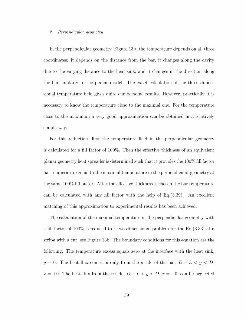
FIG. 13: Perspective views of the mounted laser bar. (a) The planar model
with the laser bar, heat spreader and heat sink describing parallel planes. Light
is emitted from the electrically pumped active regions defined by the multiple
p-contacts of width a. The center-to-center distance between p-contacts is a1,
and the thickness of the heat spreader is d. A detailed view of the laser bar is
shown in the circular inset. The inset shows that the laser bar consists of an n-
layer (n-cladding and substrate) of thickness b, a thin active region and a p-
clad of thickness b1. Different coordinate systems have been used. The
electrical resistance modeling employs the coordinate origin shown in the
inset, the thermal resistance modeling employs the coordinate origin shown in
the main drawing. (b) The perpendicular model with a similar laser bar
mounted in a grooved heat spreader. The laser bar cavity length L and heat
spreader thickness D are shown in the inset. The asymmetry of the n and p
layer thicknesses means that the heat transfer is through the p-side of the bar
which is modeled as a planar heat source of negligible thickness. 28
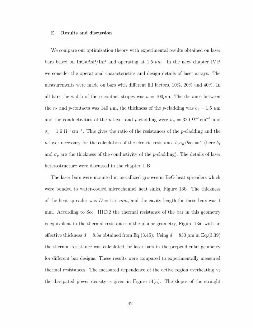
FIG. 14: Measured overheating of the active region versus dissipated power
density pdis (a) for different fill factor laser bars with 1 mm long cavities
mounted in BeO heat spreaders and (b) for different fill factor laser bars with
2 mm long cavities mounted in CuW heat spreaders. Solid symbols indicate
data points (circles, squares, and triangles for 10%, 20%, and 40% fill factors
vii
respectively). Lines fit to the experimental data are used to determine the
thermal resistance. 44
FIG. 15: Optimized fill factor (dashed line) and corresponding maximum
output power (solid line) as a function of laser temperature rise. 45
FIG. 16: Optimized fill factor (dashed line) and corresponding minimal laser
temperature rise (solid line) as a function of output power. The dotted lines
show the temperature rise for several fixed fill factor arrays as a function of
output power. 46
FIG. 17: Output power (circles) and wall-plug efficiency (squares) of a 1.5-
µm 1-D array operated in q-CW (open symbols) and CW (closed symbols)
modes at a coolant temperature of 16 oC. Inset demonstrates integrated
emission spectrum of the array measured at 40 A and 18 oC. 50
FIG. 18: Output power of a 2-D array operated in the q-cw mode at 18 oC.
Inset demonstrates integrated emission spectrum of a 2-D array recorded at 40
A and 18 oC. 52
FIG. 19: Current characteristics of output-power and wall-plug efficiency of
2.3-µm laser linear array. The light-current characteristics in cw and q-cw
were measured at 18 oC coolant temperature and at room temperature
(uncooled) in short pulse operation. The inset shows the laser array emission
spectrum measured at 30-A drive current and 18 oC coolant temperature in
CW operation. 53
FIG. 20: The experimentally measured active-region temperature rise as a
function of dissipated power is shown for different fill factor arrays. The inset
shows the dependence of the thermal resistance on fill factor. 56

viii
FIG. 21: Active-region temperature distribution over 1 mm of a 1cm long
laser bar with different fill factors at the total dissipated power of 20 W. The
inset demonstrates the analytical (solid symbols) and experimental (open
symbols) average temperature change for different FFs at given total
dissipated power of 20 W. 57
FIG. 22: Time dependence of average wavelength shift (left axis) and the
corresponding active region temperature change (right axis) for a laser diode
array with a 20% fill factor. 63
FIG. 23: Active region temperature rise divided by dissipated power (i.e.
thermal resistance) as a function of time for different FF arrays. 64
FIG. 24: The cross section geometry of the laser array assembly used for the
calculation of the temperature distribution is shown. The BeO heat spreader
occupies the region 0 < y < b. The laser bar is plotted by the line A-B. The
interface between the BeO heat spreader and the heat sink lies at y = b. 65
FIG. 25: The Active-region initial temperature rise during the first 200 µs for
10%, 20%, and 40% FF arrays at a constant total bar Pdis of 25 W. 68
FIG. 26: The temperature changes are plotted on double-log axes for the three
fill factors. The solid lines were fitted to the experimental data over the time
interval of 200 µs to 10 ms. The computed slopes are shown in the inset as a
function of the fill factor. 70
FIG. 27: The active-region temperature change of a 20% fill factor array is plotted
vs the square-root of time with 30-, 40-, and 50-A drive currents at a coolant
temperature of 18 oC. The dependency of the slope coefficient α the total

ix
dissipated power is shown for 10% (square symbol), 20% (circle symbol), and
40% (triangle symbol) fill factor arrays in the inset. 71
FIG. 28: Normalized deviation from steady-state temperature vs time is plotted
for arrays with 10%, 20%, and 40% FF. The slopes of the solid lines are used to
calculate τc, which is shown in the inset. 73

x
List of Tables
TABLE I. InGaAsP/ InP laser heterostructure. 15
TABLE II. In(Al)GaAsSb/ GaSb laser heterostructure. 21

xi
List of Publications:
Refereed Journals:
1. B. Laikhtman, A. Gourevitch, D. Westerfeld, D. Donetsky and G. Belenky,
“Thermal resistance and optimal fill factor of high power laser bar”,
Semicond. Sc. Technol. 20, 1087-1095, (2005).
2. A. Gourevitch, B. Laikhtman, D. Westerfeld, D. Donetsky, G. Belenky, C. W.
Trussell, Z. Shellenbarger, H. An, R. U. Martinelli, “Transient thermal
analysis of InGaAsP-InP high-power diode laser arrays with different fill
factors”, J. Appl. Phys., 97, 084503 1-6, (2005).
3. L. Shterengas, G.L. Belenky, A. Gourevitch, D. Donetsky, J.G. Kim, R.U.
Martinelli, and D. Westerfeld, “High power 2.3-µm GaSb-based linear laser
array”, IEEE Photon. Tech. Lett. 16, 2218-2220, (2004)
4. G. Belenky, J.G. Kim, L. Shterengas, A. Gourevitch, R.U. Martinelli, “High-
power 2.3-μm laser arrays emitting 10 W CW at room temperature”, Electron.
Lett., 40, 737-738, (2004)
5. B. Laikhtman, A. Gourevitch, D. Donetsky, D. Westerfeld, G. Belenky,
“Current spread and overheating of high power laser bars”, J. Appl. Phys., 95,
3880-3889, (2004)
6. A. Gourevitch, G. Belenky, D. Donetsky, B. Laikhtman, D. Westerfeld, C.W.
Trussell, H. An, Z. Shellenbarger, R. Martinelli, “1.47-1.49-μm InGaAsP/InP
diode laser arrays”, Appl. Phys. Lett., 83, 617-619, (2003)
7. L. Shterengas, G.L. Belenky, A. Gourevitch A, J.G. Kim, R.U. Martinelli,
“Measurements of alpha-factor in 2-2.5 μm type-I In(Al)GaAsSb/GaSb high
power diode lasers”, Appl. Phys. Lett., 81, 4517-4519 (2002)
xii
Conference Proceedings:
8. A. Gourevitch, G. Belenky, L. Shterengas, D. Donetsky, D. Westerfeld, B.
Laikhtman, R.U. Martinelli, G. Kim, “1.5 and 2.3-µm Diode Laser Arrays for
Optical Pumping”, Optics & Photonics 2005, co-located with the SPIE 50th
Annual Meeting, Proceedings of SPIE Volume: 5887, pp. 239-247, 2005
9. A. Gourevitch, D. Donetsky, G. Belenky B. Laikhtman, D. Westerfeld, Z.
Shellenbarger, H. An, R. U. Martinelli, C. W. Trussell, ”Transient thermal
analysis of 1.47-μm high power diode laser arrays“, Proceeding of the Solid
State and Diode Laser Technology Review, SSDLTR-04, P-9, 2004.
10. G. Belenky, L. Shterengas, A. Gourevitch, D. Donetsky, J. Kim, R. U.
Martinelli, D. Westerfeld, “2.3-μm GaSb-based diode laser linear arrays
emitting 10W CW at room temperature”, Proceeding of the Solid State and
Diode Laser Technology Review, SSDLTR-04, P-20, 2004.
11. G. Belenky, A. Gourevitch, D. Donetsky, D. Westerfeld, B. Laikhtman, C.W.
Trussell, H. An, Z. Shellenbarger, R. Martinelli, “1D and 2D 1.5-μm
InGaAsP-InP diode laser arrays: experiment and modeling”, Proceeding of
Lasers and Electro-Optics, CLEO 03, 432-434, 2003.
12. G. Belenky, A. Gourevitch, D. Donetsky, D. Westerfeld, C. W. Trussell, H.
An, Z. Shellenbarger, R. Martinelli, “High power 1.5-μm InGaAsP-InP Diode
Laser Arrays”, Proceeding of the Solid State and Diode Laser Technology
Review, SSDLTR-03, P-10, 2003.
13. L.Shterengas, A.Gourevich, G.Belenky, J.G.Kim, R.Martinelli,
“Measurements of alpha-factor in 2-2.5-μm type-I In(Al)GaAsSb/GaSb
broadened waveguide lasers”, Lasers and Electro-Optics, CLEO 2002.
Technical Digest., pp. 157 - 158 vol.1, 2002

I. HIGH POWER LASER ARRAYS
A. Introduction
The remarkable improvement of high-power diode lasers makes them very at-
tractive for different applications, like material processing, optical pumping, secure
free-space communication and infrared countermeasures. The key requirements for
successful commercialization of high-power laser diodes are high output power, high
efficiency, reliable operation, and low fabrication cost.
One basic approach for higher output power is to enlarge the laser diode gain
area: increase the stripe width (emitting aperture) and/or cavity length. However,
this approach encounters optical field filamentation and lateral mode instabilities,
leading to the appearance of so-called hot spots and the degradation of the laser.
Usually, the width of a single emitter does not exceed 200 µm.
Another way to increase the gain area is to increase the number of emitters
integrated side by side on a monolithic laser bar. These emitters are electrically
connected in parallel, and are optically isolated from each other. Figure 1 shows
a section of such a laser bar. The output power from laser bar scales with the
number of emitters, so each stripe can emit a moderate output power which does
not cause facet degradation. Today, commercially available high-power diode laser
arrays demonstrate output powers up to 100 W from a single bar [1–5]. Higher
output powers up to the kW-regime are obtained from stacked arrays of these bars
[6–8].
The integration of laser emitters in a monolithic bar implies some crucial prob-
1

FIG. 1: Schematic diagram of an edge emitting laser bar.
lems: 1) technological problems 2) spurious modes 3) high heat dissipation in a
relatively small volume 4) mutual heating of adjacent emitters.
The technological steps to process the laser diode bar are similar to the ones for
single laser diode, the difference is only in the mask layout. However, each process
step must be carried out to a very high reliability level. A defect of one emitter can
cause the failure of the entire bar by electrical or thermal effects.
Another problem arising from the integration of broad area emitters is the ap-
pearance of so-called spurious modes that decrease the overall output power from
the laser bar. These modes have a propagation direction perpendicular to the de-
sired output. These parasitic modes appear in bars with a high fill factor, and have
to be suppressed by increasing the optical losses for such modes. The filling factor
is the ratio of the active (pumped) area to the whole area of the laser bar. There
are several approaches to suppress spurious modes. One approach is to etch deep
grooves between the emitters. Another approach is to use the etched mesa structure
itself to create an asymmetric optical field distribution for parasitic modes, resulting
in high optical leakage from the waveguide layers into the substrate.
Recently, some groups sponsored by the Defense Advanced Research Projects
Agency (DARPA) Super High Efficiency Diode Sources (SHEDS) Program demon-
2

strated record high peak power conversion efficiencies approaching 70% [1, 2, 9, 10].
Conversion efficiency is defined as the ratio between output optical power (Pout) and
input electrical power (Pout). Usually, the conversion efficiency varies significantly
for laser diodes based on different semiconductor materials and is less than 50%. As
a result, a considerable amount of heat is generated in diode lasers and laser bars
during high-power operation. The relatively small size of diode laser bars results in
a relatively high thermal resistance Rth, which is defined as the temperature rise of
the active region divided by the dissipated power:
Rth =∆T
Pin − Pout(1.1)
Depending on the thermal resistance, the heat dissipation in laser diodes results in
an active region temperature rise. This temperature rise limits the output power
(through so-called thermal rollover) and enhances the device degradation mecha-
nisms. It is therefore critical to minimize the thermal resistance in high-power laser
devices.
The close proximity of adjacent laser emitters results in an overlapping of heat
fluxes from neighboring stripes. The overlapping of heat fluxes leads to an additional
temperature rise due to mutual overheating of adjacent stripes [11, 12]. However,
it was shown in Ref. [13] that the thermal resistance decreases with increased
filling factor. A detailed analysis of fill factor influence on laser bar overheating is
considered in chapter III.
In this dissertation, progress in the development of high-power infrared laser
arrays is discussed, including the development of InP-based and GaSb-based laser
3
arrays operating at 1.5-µm and 2.3-µm, correspondingly. The different aspects of
laser array design, thermal analysis and laser bar optimization have been studied
analytically and experimentally.
B. Applications of 1.5-µm high-power laser arrays
Optically pumped erbium doped solid state lasers operating between the 4I13/2
and 4I15/2 laser transition are well suited for the production of high power eye-
safe laser light between 1.5 - 1.65-µm. These lasers provide the combination of
beam quality, efficiency, and high optical power required for different applications.
Erbium doped solid state lasers are typically pumped at a wavelength between 940
and 980 nm (∼ 1.3 eV/photon) and emit in the eye-safe region 1.5 - 1.65-µm (∼0.8
eV/photon). The difference in energy between the pump light photons and the laser
emission photons is known as the quantum defect, and represents energy that is lost
to heat in the solid state laser. The quantum defect for our example laser is near 0.5
eV; at least 38% of the pumping optical power is wasted to heat due to the quantum
defect alone.
This inefficiency is undesirable anywhere in the high power laser system, but it
is particularly undesirable to apply high heat loads in the solid state laser medium.
High temperatures in the solid state laser material limit both the output beam
power and quality. A temperature gradient in the laser material leads to an index-
of-refraction gradient which induces self-focusing and degrades beam quality. It may
be possible to compensate for this index variation through advanced design, but this
becomes increasingly difficult in the presence of thermal transients. Non-uniform
4

heating also introduces mechanical forces that can lead to crystal fractures. Finally,
the solid state laser structure is poor from a heat transport perspective; the long
path from the pumped region to the cooled periphery acts to virtually guarantee
large temperature variations if the laser is pumped with a high quantum defect
source. Various designs (e.g. the spinning disk solid state laser) have been proposed
to address the heating problem, each with its own disadvantages.
There are more difficulties associated with high quantum defect solid state laser
pumping schemes. One of these difficulties lies in the requirement for sensitizer
atoms (typically ytterbium for erbium based lasers) to be co-doped into the solid
state host material. These sensitizer atoms allow for efficient absorption of the rel-
atively shortwave length pump light, but their use places constraints on the erbium
concentration, which in turn constrains the gain, absorption and energy storage
capability of the solid state laser.
Sensitizer atoms and a high quantum defect combine to facilitate up conversion,
process whereby already excited dopant atoms absorb additional energy and enter
very high energy states that do not contribute to the 1.5 - 1.65-µm laser emission.
This process depletes the upper laser state population, while simultaneously wasting
pump power and increasing host heating.
An alternative to high quantum defect pumping is to pump directly into the
upper part of the narrow band of energies available to excited Erbuim atoms [14–
19]. This near resonant pumping scheme requires high power laser diodes that can
put a large fraction of their output energy in a fairly narrow energy band. This
pump light spectral precision must be maintained over a range of diode operating
5

FIG. 2: Absorption (blue line) and emission (red) for Er:YAG
temperatures. Figure 2 shows the absorption and emission spectra for a Er:YAG
laser material. In this material, absorption of pump light in the 1.47 - 1.49-µm
region can be used to generate emission at 1.5 - 1.64-µm, for a quantum defect of
only around 0.06 eV. Semiconductor sources can be tailored to deliver their energy
into the spectral region required by the solid state laser designer. The material in
Figure 2 can also be pumped at 1.52-µm for emission at 1.64-µm [17]. There are
technical challenges for such a system, but the resulting quantum defect of only
a few thousandths of an eV makes this approach very attractive. These quantum
defects are two orders better than is obtained with traditional high quantum defect
pumping methods.
6

C. Applications of 2.3-µm high-power laser arrays
Diode laser arrays operating in the spectral range 2 - 3-µm are promising as com-
pact and efficient light emitters for different applications. Atmospheric transparency
in the 2.0 - 2.4-µm region permits applications as diverse as secure free-space com-
munication and infrared countermeasures (IRCM). Further, these lasers are ideally
suited for use as pump sources for new solid state and optically pumped semi-
conductor sources operating in the mid-infrared atmospheric transparency windows
between 3.5-µm and 5.0-µm.
Type-I GaSb-based semiconductor lasers operate up to 2.85-µm [20] and output
hundreds of milliwatts in continuous-wave (CW) mode at room temperature [21–
29]. These devices can be used as low quantum-defect pumping sources for a new
generation of optically pumped semiconductor lasers operating in band-II of the
atmospheric transparency [30]. High-power CW laser arrays based on InP material
system were fabricated with the longest wavelengths of 1.9-µm (11 W per 1 cm bar)
[31] and 2-µm (8.5 W per 1 cm bar) [32]. Further increasing the operating wave-
length within the InP-based material system leads to dramatic laser performance
degradation. The longest reported operating wavelength of the diode laser arrays
was 2.05-µm achieved with In(Al)GaAsSb/GaSb material system [33] though the
array was not designed to work in high-power CW regime.
As an example of the advantages of high-power 2.3-µm pump arrays, we will con-
sider the 4-µm type-II lasers recently reported by the Air Force Research Laboratory
[34]. As can be seen in Figure 3, these devices have an active region consisting of
7

FIG. 3: Schematic band diagram showing the energy gap sequence of two repetitions of
an InAs/InGaSb/InAs active region, three repetitions of InGaAsSb integrated absorbers,
and one clad layer. Dashed lines represent upper and lower lasing levels
multiple layers of InAs and InGaSb sandwiched between integrated absorber (IA)
layers of InGaAsSb. Light emission is due to transitions between electrons confined
in the InAs wells and holes confined in the InGaSb wells [35]. Carriers are provided
by absorption of pump radiation in the quaternary integrated absorber layers.
The alloy composition of the IA layers is chosen for lattice matching to the GaSb
substrate, and also to provide an appropriate band gap for efficient absorption of the
pump radiation. The energy difference between the pump photons and the emitted
photons is known as the quantum defect, and this energy is dissipated by heating
the laser structure.
Since device heating adversely affects the devices performance, it is desirable to
minimize the quantum defect. Recently, type-II lasers have been pumped with 1.85-
8

µm laser light (0.67 eV pump photon energy). These type-II devices emit light at
around 4.0-µm (0.31 eV), producing a quantum defect of 0.36 eV. The proposed
2.3-µm source emits photons with energy of 0.54 eV, yielding a quantum defect of
just 0.23 eV. By switching from the 1.85-µm pump sources to 2.3-µm pump sources
the quantum defect is reduced by 36%.
There are limits as to how much the quantum defect can be reduced in these struc-
tures. In particular, the edge of the miscibility gap for lattice matched GaInAsSb
will cause problems in designing the IA for wavelengths much longer than 2.3-µm
[36].
9
II. PERFORMANCE OF INFRARED LASER DIODES
A. Introduction
InGaAsP/InP is one of the basic material systems of modern optoelectronics.
Well-developed metal organic chemical vapor deposition (MOCVD) technology al-
lows for high yield fabrication of InP-based lasers in the wavelength range from
1-µm to 2-µm. The region between 2-µm and 3-µm is well handled by type-I
laser devices based on the GaSb material system, grown by molecular beam epitaxy
(MBE). Recently, lasers with continuous-wave operation up to 3.04-µm have been
demonstrated [22, 38, 39]. These lasers comprise compressively strained GaInAsSb
quantum wells (QWs) with indium concentrations up to 50% and lattice matched
AlGaAsSb barriers and waveguides.
In this chapter we consider the details of laser heterostructure design of diode
lasers operating at 1.5-µm and 2.3-µm wavelength. The design of both lasers is
focused on high-power operations. That requires low threshold current and high
efficiency. The common feature of both designs is a broadened-waveguide layer.
The broadened waveguide (BW) approach reduces overlap of the optical field with
highly doped cladding layers and minimizes the optical losses due to free carrier
absorption [40]. This chapter is organized as follows. In section IIB we present
the design and performance details of InP-based single emitters. In section IIC the
design and performance of GaSb-based single lasers are considered.
10

B. Design and performance of 1.5-µm single lasers
The InGaAsP/InP laser structure emitting at 1.5-µm was grown by metalloor-
ganic chemical vapor deposition. The schematic energy band-gap diagram of laser
structure is shown on Figure 4. The active region contains three 6-nm InGaAsP
quantum wells (QWs) with 1% compressive strain separated by 16-nm InGaAsP
barriers. A double-step graded-index separate confinement heterostructure (SCH)
with 300-nm-thick outer and 30-nm-thick inner InGaAsP layers provides optical
confinement. The broadened waveguide (710 nm) was incorporated between n- and
p-clad layers, each 1.5-µm thick. The n-cladding was doped with Se with a concen-
tration of 5 ∗ 1017cm−3 and the p-cladding was gradually doped with Zn with an
average concentration of 7.5 ∗ 1017cm−3. Zn doping of the p-cladding was optimized
to exhibit optical losses as low as 2-3 cm−1 [41, 42]. All layers, the composition
and thickness of which are given in Table I, except the QWs were grown lattice-
matched to the InP substrate. The total thickness of the laser structure including
the substrate was 140 µm. Details of the laser heterostructure design were reported
elsewhere [41–44].
The wafer was processed into single emitters. The laser emitters had 100-
µm stripe width, 1-mm and 2-mm cavity length. The laser facets were high-
reflection/antireflection coated with reflection coefficients of 95% and 3%, respec-
tively. These lasers were indium-soldered epi-side down onto copper heat sinks and
were characterized.
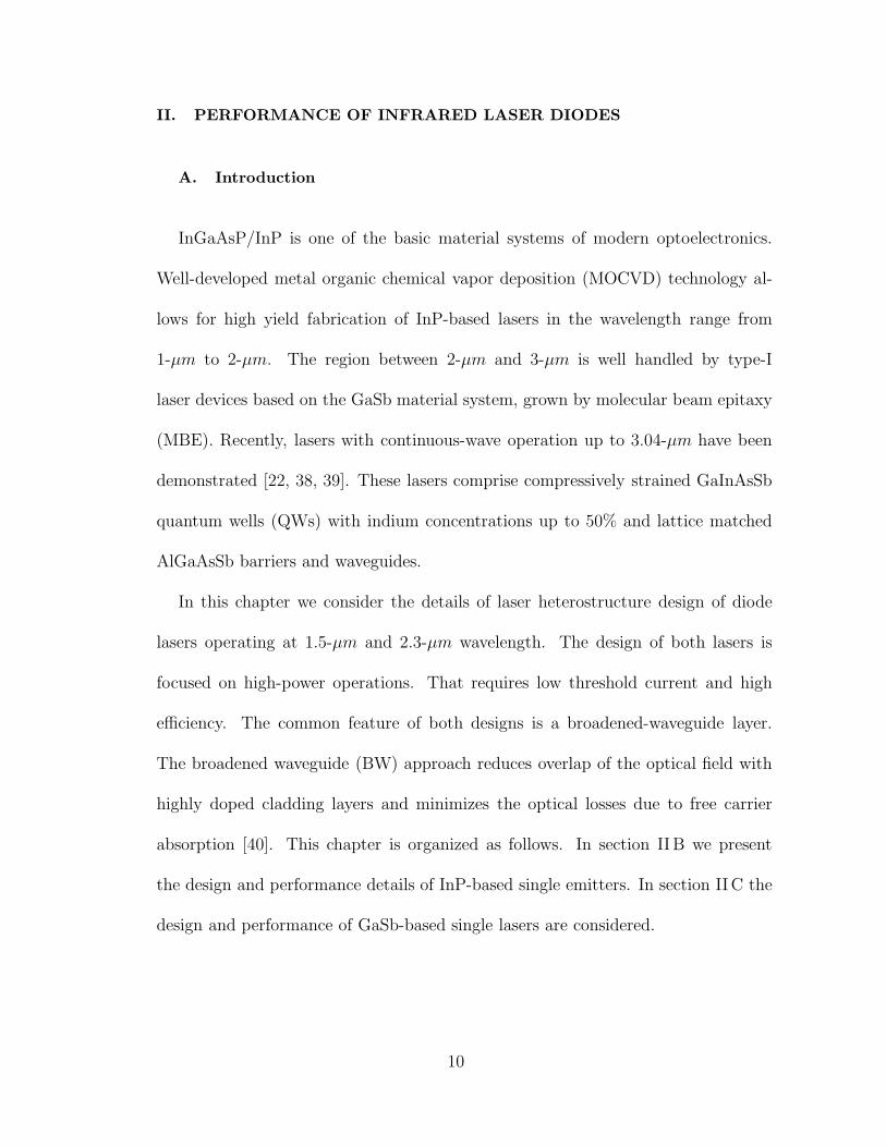
Figure 5 shows CW current characteristics of output power and wall-plug effi-
11

FIG. 4: Schematic energy band diagram of the broadened waveguide 1.5-µm wavelength
InGaAsP/InP laser.
ciency for 1-mm and 2-mm-long single lasers, measured at a heat sink temperature
of 18 C. The lasers output 1.2 W and 2.2 W in CW operation. The wall-plug effi-
ciency of 28% and 30% peaked at 2 A and 3 A for the 1-mm and 2-mm-long single
lasers, correspondingly. The far field radiation pattern was measured for a single
laser at 1.5 A CW drive current. The fast axis divergence was 44o FWHM, the slow
divergence 8o FWHM.
Figure 6 shows the performance of 100-µm-wide 1-mm-long single laser measured
in pulse operation (200 ns, 1 MHz) at different heat sink temperatures. The thresh-
old current density was around 480 A/cm2 and a differential efficiency was 60 % at
a 20 oC. Over the temperature range from 20 to 70 oC, the threshold characteristic
temperature T0 was 54 K and the slope-efficiency characteristic temperature T1 was
160 K, Figure 7.
12
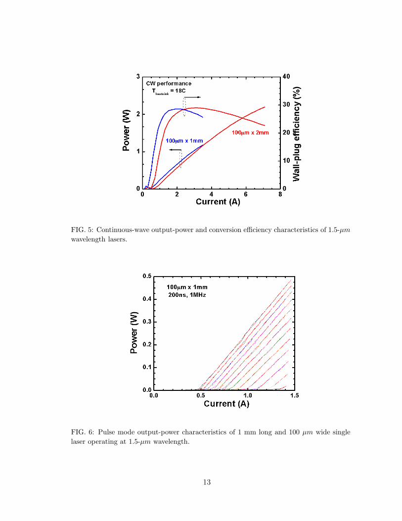
FIG. 5: Continuous-wave output-power and conversion efficiency characteristics of 1.5-µm
wavelength lasers.
FIG. 6: Pulse mode output-power characteristics of 1 mm long and 100 µm wide single
laser operating at 1.5-µm wavelength.
13
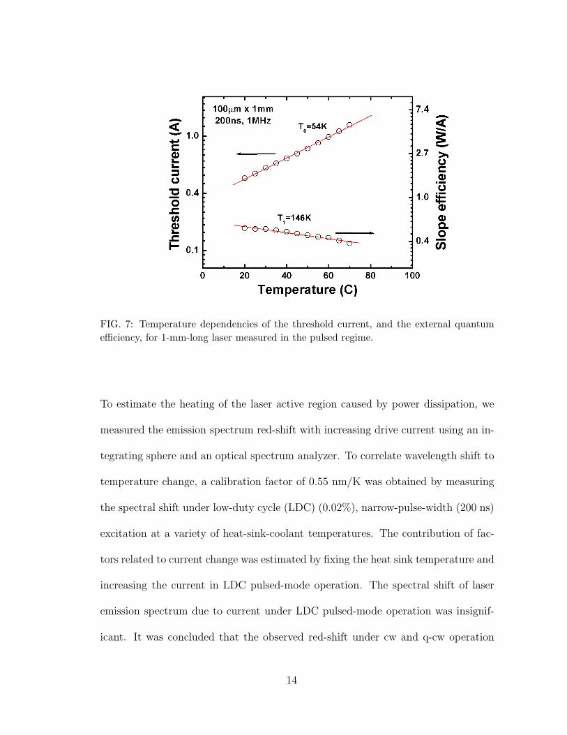
FIG. 7: Temperature dependencies of the threshold current, and the external quantum
efficiency, for 1-mm-long laser measured in the pulsed regime.
To estimate the heating of the laser active region caused by power dissipation, we
measured the emission spectrum red-shift with increasing drive current using an in-
tegrating sphere and an optical spectrum analyzer. To correlate wavelength shift to
temperature change, a calibration factor of 0.55 nm/K was obtained by measuring
the spectral shift under low-duty cycle (LDC) (0.02%), narrow-pulse-width (200 ns)
excitation at a variety of heat-sink-coolant temperatures. The contribution of fac-
tors related to current change was estimated by fixing the heat sink temperature and
increasing the current in LDC pulsed-mode operation. The spectral shift of laser
emission spectrum due to current under LDC pulsed-mode operation was insignif-
icant. It was concluded that the observed red-shift under cw and q-cw operation
14
was caused by the heating of the active region.
Layer Composition Thickness (nm)
p-clad InP:Zn 1500
Outer SCH InGaAsP (1.13 eV) 300
Inner SCH InGaAsP (1 eV) 30
Barrier (2) InGaAsP (1 eV) 16
QW (3) InGaAsP (0.8 eV) 1% of compressive strain 6
Inner SCH InGaAsP (1 eV) 30
Outer SCH InGaAsP (1.13 eV) 300
n-clad InP:Se 1500
TABLE I. InGaAsP/ InP laser heterostructure.
C. Design and performance of 2.3-µm single lasers
The laser heterostructure was grown by solid source molecular-beam epitaxy
on n-GaSb substrates. The schematic energy band-gap diagram of laser structure
is shown on the Figure 8. An 830 − nm-thick undoped Al0.25Ga0.75As0.02Sb0.98
broadened-waveguide layer including the two quantum wells (QWs) is sandwiched
between two 2−µm-thick Al0.9Ga0.1As0.07Sb0.93 cladding layers. Two 200-nm-spaced
11.5-nm-wide In0.41Ga0.59As0.14Sb0.86 QWs provided optical gain. The n-cladding
was Te-doped to 3 ∗ 1017cm−3. The p-cladding was Be-doped to 1 ∗ 1018cm−3 over
15
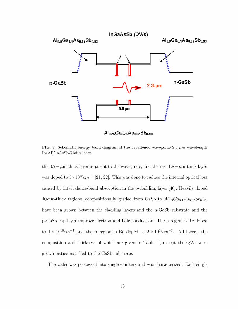
FIG. 8: Schematic energy band diagram of the broadened waveguide 2.3-µm wavelength
In(Al)GaAsSb/GaSb laser.
the 0.2−µm-thick layer adjacent to the waveguide, and the rest 1.8−µm-thick layer
was doped to 5∗1018cm−3 [21, 22]. This was done to reduce the internal optical loss
caused by intervalance-band absorption in the p-cladding layer [40]. Heavily doped
40-nm-thick regions, compositionally graded from GaSb to Al0.9Ga0.1As0.07Sb0.93,
have been grown between the cladding layers and the n-GaSb substrate and the
p-GaSb cap layer improve electron and hole conduction. The n region is Te doped
to 1 ∗ 1018cm−3 and the p region is Be doped to 2 ∗ 1019cm−3. All layers, the
composition and thickness of which are given in Table II, except the QWs were
grown lattice-matched to the GaSb substrate.
The wafer was processed into single emitters and was characterized. Each single
16
gain-guided element aperture was 100 µm defined as a window in a 0.2 µm-thick
SiN dielectric layer. The facets were coated to reflect 3% and 95%. Single lasers
were indium-soldered epi-side down onto copper heat sinks.
Figure 9 shows CW light-current characteristics and wall-plug efficiency for a
1-mm-long single 2.3-µm laser, taken at a heat sink temperature of 16 C. The
output power was recorded by a 50-mm-diameter thermopile detector. The CW
near threshold slope efficiency and threshold current were 0.2 W/A and 0.4 A. The
output power saturated with current due to heating. Single lasers output 650-mW
CW at 3.8 A. The wall-plug efficiency of 12% peaked at 1A. The output spectrum
(insert in Figure 2) was centered near 2.36 µm; its full-width at half-maximum
(FWHM) was about 14 nm at a current 2-A CW. The FWHM of the transverse
far-field pattern is about 63o and is current independent.
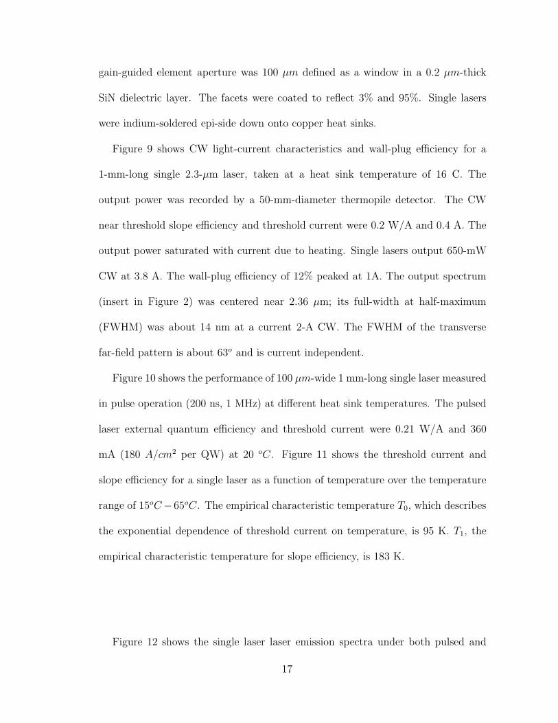
Figure 10 shows the performance of 100 µm-wide 1 mm-long single laser measured
in pulse operation (200 ns, 1 MHz) at different heat sink temperatures. The pulsed
laser external quantum efficiency and threshold current were 0.21 W/A and 360
mA (180 A/cm2 per QW) at 20 oC. Figure 11 shows the threshold current and
slope efficiency for a single laser as a function of temperature over the temperature
range of 15oC−65oC. The empirical characteristic temperature T0, which describes
the exponential dependence of threshold current on temperature, is 95 K. T1, the
empirical characteristic temperature for slope efficiency, is 183 K.
Figure 12 shows the single laser laser emission spectra under both pulsed and
17

FIG. 9: Continuous-wave output-power and conversion efficiency characteristics of 2.3-µm
wavelength lasers.
CW operation. To correlate wavelength shift to temperature change, we measured
the spectral shift under narrow-pulse-width (200 ns) excitation at a variety of heat-
sink-coolant temperatures, Figure 12a. The calibration factor of 1.2 nm/K was
determined from the obtained data. The peak laser wavelength increases with tem-
perature from about 2.33-µm at 20 C up to 2.38-µm at 60 C due to band gap
reduction with increasing temperature, Figure 12b. The full-width, half-maximum
(FWHM) spectral width was approximately 10 nm at a drive current of 1.5 A,
broadening to 18 nm at a drive current of 3 A.
18
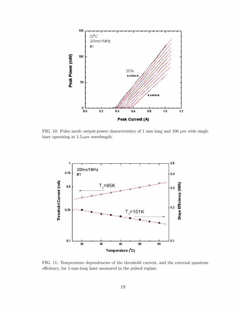
FIG. 10: Pulse mode output-power characteristics of 1 mm long and 100 µm wide single
laser operating at 1.5-µm wavelength.
FIG. 11: Temperature dependencies of the threshold current, and the external quantum
efficiency, for 1-mm-long laser measured in the pulsed regime.
19
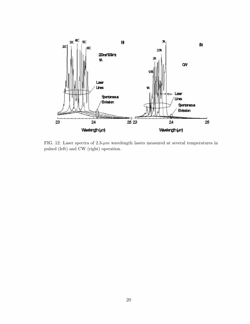
FIG. 12: Laser spectra of 2.3-µm wavelength lasers measured at several temperatures in
pulsed (left) and CW (right) operation.
20
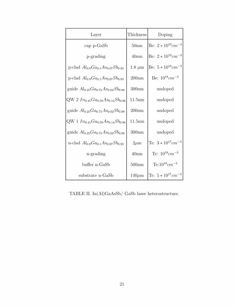
Layer Thickness Doping
cap p-GaSb 50nm Be: 2 ∗ 1019cm−3
p-grading 40nm Be: 2 ∗ 1019cm−3
p-clad Al0.9Ga0.1As0.07Sb0.93 1.8 µm Be: 5 ∗ 1018cm−3
p-clad Al0.9Ga0.1As0.07Sb0.93 200nm Be: 1018cm−3
guide Al0.25Ga0.75As0.02Sb0.98 300nm undoped
QW 2 In0.41Ga0.59As0.14Sb0.86 11.5nm undoped
guide Al0.25Ga0.75As0.02Sb0.98 200nm undoped
QW 1 In0.41Ga0.59As0.14Sb0.86 11.5nm undoped
guide Al0.25Ga0.75As0.02Sb0.98 300nm undoped
n-clad Al0.9Ga0.1As0.07Sb0.93 2µm Te: 3 ∗ 1017cm−3
n-grading 40nm Te: 1018cm−3
buffer n-GaSb 500nm Te:1018cm−3
substrate n-GaSb 140µm Te: 5 ∗ 1017cm−3
TABLE II. In(Al)GaAsSb/ GaSb laser heterostructure.
21
D. Conclusion
In this chapter
• We present the heterostructure designs of laser diodes lasing at 1.5-µm and
2.3-µm.
• The laser diodes operating at 1.5-µm output up to 2.2 W in cw mode. The
peak wall-plug efficiency was 30%.
• The GaSb-based laser diode demonstrated a cw output power of 0.65 W at
2.3-µm wavelength. The conversion efficiency peaked at 9%.
22
III. THERMAL RESISTANCE AND OPTIMAL FILL FACTOR OF A
HIGH POWER DIODE LASER BAR
A. Introduction
A growing demand for high power optical sources led to a race to improve device
reliability and increase output power. Technological development produced a grad-
ual increase of single laser output power, however, a significant improvement took
place with the fabrication of laser bars. The laser bar contains numerous individual
laser emitters arranged side-by-side to form a single monolithic array. A typical
laser bar might contain twenty 100 µm wide emitters equally spaced to span a 1 cm
wide bar. The fill factor for such an array is defined to be the ratio of pumped bar
area to total bar area.
Two solutions are most evident for increasing the laser bar output power: one
is to increase the current per emitter, and the other is to increase the number
of emitters. Increasing the number of fixed-width emitters on a fixed-width bar
is equivalent to reducing the distance between individual emitters (i.e. increasing
the fill factor). Both solutions, however, encounter an overheating problem. An
increased pumping current leads not only to an increased output power but also, due
to limited efficiency, to an increased dissipated power. As a result, the temperature
in the active region grows which reduces the carrier confinement and increases the
rate of non-radiative recombination processes. This causes an efficiency reduction
so that eventually the output power saturating with increased pumping current
(thermal rollover) [45].
23
Reducing the distance between emitters operating at constant dissipated power
results in a similar heating problem. Decreasing the separation between adjacent
emitters in a laser bar causes mutual heating which also leads to an active region
temperature rise and decreased efficiency [11, 12]. A natural step is to reduce the
distance between the emitters while also varying the pumping current in such a way
that the total output power would increase. That is, we come to the problem of the
optimal fill factor: finding the fill factor that allows for maximal laser bar output
power.
Practically, however, laser bars are not normally operated in the regime of maxi-
mal output power. The laser temperature in this regime is quite high which reduces
the device lifetime. The reliability issue leads to other approaches to the optimiza-
tion problem: optimization of the distance between emitters to produce 1) maximal
output power for a given active region temperature rise or 2) minimal active region
temperature rise for a given output power.
Basically, all these approaches are related to the general problem of the optimiza-
tion of the laser bar design. The search for the optimal fill factor when all other
elements of the laser geometry (e.g., the width of the contact stripes) are fixed is an
approach that allows an exact mathematical solution.
The calculation of the optimal fill factor is based on the standard phenomeno-
logical equations that describe the operation of a laser bar [45–47]. Some of the
main parameters in these equations, namely, the thermal resistance characterizing
the cooling rate and the series resistance characterizing the power dissipated away
from the active region, depend on the fill factor. The dependence is controlled by
24

the laser design. The analytical expressions for the thermal and electrical series
resistance for typical laser bar designs are determined, and then these expressions
are used to find the optimal fill factor for a given laser bar architecture.
The central point in the evaluation of the electric resistance is the current spread
calculation. In some previous publications the current density was calculated under
the assumption of constant density at the contact stripe which then falls off as the
square of the distance away from the contact [48–54]. An exact analytical solution
to the Laplace equation that controls the current spread when carrier diffusion can
be neglected was obtained by Lengyel et al. [55]. They studied a narrow stripe
geometry where the width of the stripe is of the order of its distance from the active
region. Similar models have been considered by Wilt [56], Joyce [57], and Agrawal
[58]. A comprehensive comparison of these models has been made by Papannareddy
at al. [59]. The geometry considered by Lengyel et al. [55] corresponded to the
situation in ridge lasers. In high power lasers the width of the stripe is much larger
than the cladding thickness, and the n-layer thickness is comparable to the stripe
width. Previously, it has been shown that such a relation leads to a high current
density near the edges of the active region [60].
The thermal resistance substantially depends on the thermal conductivity and
geometry of the heat spreader located between the laser and the heat sink [61, 62].
Determining the thermal resistance requires the solution of the thermal conductance
equation with non-trivial boundary conditions. For this purpose, a finite element
method is typically used [13, 63]. However, the analytical approach allows one to
understand the qualitative dependence of device characteristics on different param-
25
eters without performing time consuming numerical calculation required in finite
element methods.
The calculated electrical series resistance is weakly dependent on fill factor. In
contrast, the dependence of the thermal resistance on the fill factor is substantial.
The expression obtained for the thermal resistance gives an excellent agreement with
measured values without any adjustable parameters [43]. Analytical results for both
resistances facilitate the calculation of the optimal fill factor.
The chapter is organized as follows. The fill factor optimization problem is formu-
lated for a laser bar in Section IIIB. In sections IIIC and IIID we present analytical
solutions to the electrical and thermal problems and calculate the electric and ther-
mal resistances. In Sec. III E we compare the theoretical and experimental values
of the thermal resistance and present the theoretical results of the bar optimization.
B. Optimal fill factor
We consider a laser bar with N contact stripes with a distance a1 between their
centers, Figure 13a. The laser bar is mounted on a heat spreader which conducts
heat from the laser bar to the heat sink. The heat sink is assumed ideal, i.e., its
temperature is fixed and does not depend on the power dissipated in the bar. We
assume that the cooling conditions for all lasers in the bar are the same and we can
neglect the edge effects. In other words, the difference between the cooling of the
lasers close to the ends of the bar and those in the middle can be neglected and
the temperature of their active regions is the same. Indeed, we did not detect any
temperature difference between different lasers in a 25 W 1.47 µm laser array that
26
contained 20 elements [43] (compare with Ref. [11, 12]).
If jth is the threshold current in one emitter and j > jth is the pumping current
then the optical power generated in this emitter is
popt = η(j − jth) (3.1)
where η is the differential efficiency. Well above the threshold the voltage drop across
the active region, U0 does not depend on the current and the power dissipated in
one laser is
pd = U0j + rj2 − popt , (3.2)
where r is the series resistance of one laser.
To make the result more general and avoid specifying the number of emitters (N)
in a bar and the length of the bar it is convenient to deal with power dissipated per
unit length of the bar, Npd/Lb, where Lb is the length of the bar. The temperature
of the active region is connected to the power dissipated per unit length by the
relation T = RT (Npd/Lb) where RT is the thermal resistance of the unit length of
the bar. At this stage it is convenient to introduce the fill factor that is defined as
f =Na
Lb
(3.3)
where a is the width of the stripe. Then with the help of Eqs.(3.1) and (3.2) the
active region temperature can be expressed as
T =fRT
a[ηjth + (U0 − η)j + rj2] . (3.4)
27
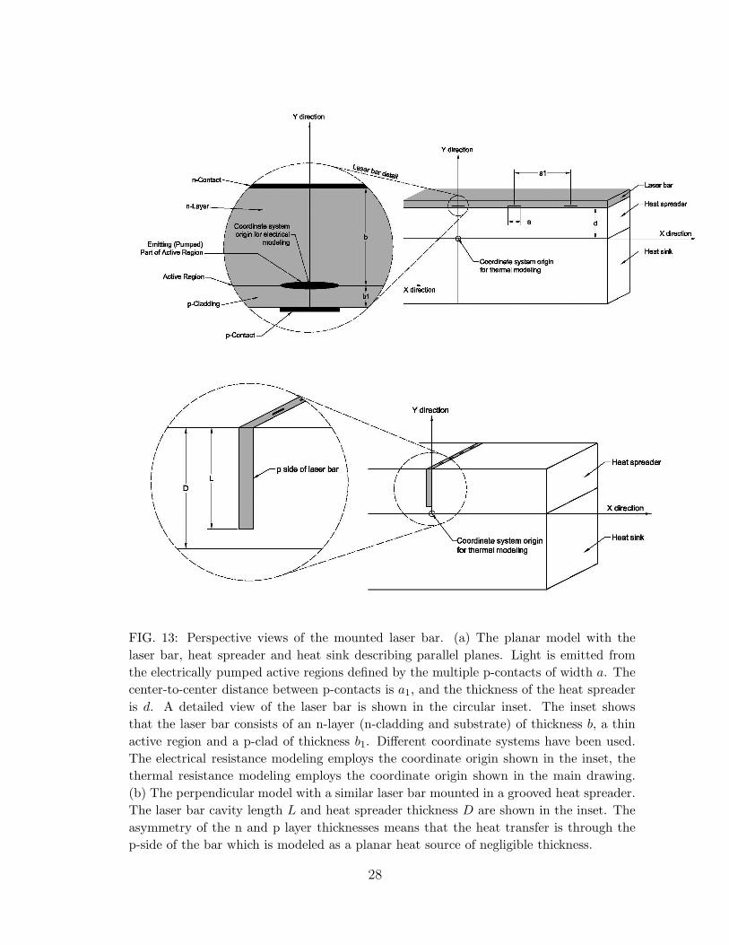
FIG. 13: Perspective views of the mounted laser bar. (a) The planar model with the
laser bar, heat spreader and heat sink describing parallel planes. Light is emitted from
the electrically pumped active regions defined by the multiple p-contacts of width a. The
center-to-center distance between p-contacts is a1, and the thickness of the heat spreader
is d. A detailed view of the laser bar is shown in the circular inset. The inset shows
that the laser bar consists of an n-layer (n-cladding and substrate) of thickness b, a thin
active region and a p-clad of thickness b1. Different coordinate systems have been used.
The electrical resistance modeling employs the coordinate origin shown in the inset, the
thermal resistance modeling employs the coordinate origin shown in the main drawing.
(b) The perpendicular model with a similar laser bar mounted in a grooved heat spreader.
The laser bar cavity length L and heat spreader thickness D are shown in the inset. The
asymmetry of the n and p layer thicknesses means that the heat transfer is through the
p-side of the bar which is modeled as a planar heat source of negligible thickness.
28

The optical power per unit length of the bar, Popt = Npopt/Lb, with the help of
Eq.(3.1) can be written as
Popt =fη
a(j − jth) . (3.5)
The definition of Popt and T by Eqs.(3.4) and (3.5) is not complete for two reasons.
The first is that jth and η depend on T . With good accuracy this dependence is
usually described as
jth = jre(T−Tr)/T0 , (3.6a)
η = ηre−(T−Tr)/T1 , (3.6b)
where Tr is the reference temperature and constants jr, ηr, T0, and T1 depend on
the details of the laser structure.
The second reason is more serious and presents the main technical difficulty for
the calculation of the optimal fill factor. Namely, both the thermal resistance and
the series resistance depend on the fill factor. This dependence is controlled by the
geometry of the laser structure and the heat spreader. The calculation of RT (f)
and r(f) is the main content of the chapter.
Equations (3.4) and (3.5) with known jth(T ), η(T ), RT (f), and r(f) make up
the basis for the optimization problems described above, and these problems can be
formulated as
• Given T , find maximal Popt .
• Given Popt, find minimal T .
It is necessary to note that mathematically the two problems are equivalent.
Given Popt(j, T, f) and T (j, f), both of them are reduced to the solution of the
29
equation
∂Popt
∂f
∂T
∂j− ∂Popt
∂j
∂T
∂f= 0 . (3.7)
together with one of Eqs.(3.4) and (3.5). The equivalence can be seen from the
results, Figures 15 and 16, where the plots Popt(T ) and T (Popt) can be obtained
from each other by the transposition of the axes.
In the next two sections we present the calculation of RT (f) and r(f) for sim-
ple but practically important models. For both cases we succeeded in obtaining
analytical results that are quite flexible and convenient for practical applications.
C. Electric resistance of the bar
The model of the laser structure used for calculating the electric resistance is
shown in Figure 13a. It consists of a p-cladding and n-layer (n-cladding with a sub-
strate) separated by a thin region containing the waveguide and quantum wells.[62]
The thickness of this quantum well region is typically smaller than 1 µm and we
consider it as an interface. The n-side of the bar is uniformly covered by a metal
n-contact, the p-side of the bar has multiple p-contact stripes of width a and center-
to-center separation a1. The thickness of the p-cladding b1 is much smaller than the
thickness of the n-layer b and the stripe width a. Previously, we considered a similar
structure with one stripe.[60] In the system with many stripes current spreads from
adjacent stripes limit each other and as a result, the resistance of the structure de-
creases with increasing distance between the stripes. We consider a bar with a large
number of stripes so that the difference of the current spread around two stripes at
30

the edges of the bar can be neglected. Then it is possible to consider a periodical
system of stripes with period a1 and fill factor f = a/a1.
Due to the small thickness of the p-cladding, the current spread in it can be
neglected and the width of the pumped active region is the same as the stripe width.
If the current density components in the p-cladding are jx = 0, jy(x, y) = jy(x, 0)
and the potential at the contact stripe, U , is constant then the potential at the
n-side of the active region is
Ua(x) = U − σpjy(x, 0) − U0 , (3.8)
where σp is the conductivity of the p-cladding and U0 is the potential drop across
the active region which is assumed constant above threshold.
The current spread problem for the n-layer now can be solved independently of
the p-cladding. Due to high doping in the n-layer the screening radius there is very
small which makes the diffusion current negligible compared to the drift current. As
a result, the potential distribution in the n-layer φ(x, y) is controlled by the Laplace
equation. One of the boundary conditions for this equation is a constant potential
at the n-contact, y = b. At the pn interface the potential is Ua(x) which can be
considered given only in the pumped regions while between the pumped regions the
current normal to the interface is zero. The solution to this problem allows one to
find jy(x, 0) as a functional of Ua(x). The substitution of this functional in Eq.(3.8)
provides an equation for Ua(x). The solution to this equation gives the final result.
In Sec. IIIC 1 the potential distribution in the n-layer is found analytically, in Sec.
IIIC 2 the potential Ua(x) is found with the help of a variational method, and in
31
Sec. IIIC 3 the resistance of the structure is calculated.
1. Potential distribution in n-layer
The boundary problem for the Laplace equation in the n-layer formulated above
is equivalent to the boundary problem for the complex potential,
χ(z) = φ(x, y) + iψ(x, y) , (3.9)
where z = x+iy. Apparently, χ(z+a1) = χ(z) and it is enough to consider the period
|x| < a1/2. The system is symmetric with respect the lines x = ±a1/2 in the middle
between the stripes, and the current normal to this line is zero, σn[∂φ/∂x]x=±a1/2 = 0
(σn is the conductivity of the n-layer). Then due to Cauchy-Riemann relations,
∂φ
∂x=∂ψ
∂y,
∂ψ
∂x= −∂φ
∂y, (3.10)
the boundary conditions can be written as
φ = Ua(x) , −a2< x <
a
2, y = 0 , (3.11a)
ψ = const. ,a
2< |x| < a1
2, y = 0 , (3.11b)
ψ = const. , x = ±a1
2, (3.11c)
φ = 0 , y = b . (3.11d)
To solve this problem it is convenient to map it first to the upper half plane of
another complex variable w = u + iv. This can be done with the help of the
transformation (see, e.g., Ref. [64, 65])
z = CF (arcsinw; k) , (3.12)
32

where F (θ; k) is the elliptic integral of the first kind. Constants C and k < 1 are
defined by the condition that point z = a1/2 is mapped onto w = 1 and point
z = a1/2 + ib is mapped onto w = 1/k,
a1 = 2CK(k) , (3.13a)
b = CK(k′) . (3.13b)
where K(k) = F (π/2; k) is the complete elliptic integral of the first kind and
k′ =√
1 − k2. When w → ∞ Eq.(3.12) gives z = ib. The transformation inverse to
Eq.(3.12) is expressed in elliptic sinus,
w = sn(z; k) . (3.14)
Now it is necessary to find the function χ(w) = φ(u, v) + iψ(u, v) analytic at the
upper half plane of w and satisfying the following boundary conditions at v = 0:
φ = (U − U0)Φ(u) , −ua < u < ua , (3.15a)
ψ = const. , ua < |u| < 1/k , (3.15b)
φ = 0 , |u| > 1/k . (3.15c)
where
ua = sn(a/2C; k) < 1 , (3.16)
Φ(u) =1
U − U0Ua[CF (arcsin u; k)] . (3.17)
The solution to this problem can be found with the help of the Keldysh - Sedov
method Ref. [65, 66] and is [60]
χ(w) =U − U0
π[−f(w) + ψ0g(w)] , (3.18)
33
where
f(w) = 2w√
(1 − k2w2)(w2 − u2a)
∫ ua
0
Φ(t)√
(1 − k2t2)(u2a − t2)
dt
t2 − w2,(3.19a)
g(w) = 2w√
(1 − k2w2)(w2 − u2a)
∫ 1/k
ua
1√
(1 − k2t2)(t2 − u2a)
dt
t2 − w2.(3.19b)
Here√
1 − k2w2 is defined on the plane of w with the cuts along the real axis from
w = 1/k to ∞ and from w = −1/k to −∞, and is positive at the real axis between
the points −1/k and +1/k.√
w2 − u2a is defined on the plane of w with the cut
along the real axis between the points w = −ua and w = ua and positive at the real
axis at u > ua. Thus the function√
(1 − k2w2)(w2 − u2a) is real and positive at the
real axis between the points ua and +1/k and changes sign when w changes sign.
The integrals in both f(w) and g(w) are defined at the upper half-plane of w. They
can be analytically continued to the lower half-plane across the part of the real axis
where they are real.
Potential χ(w) is limited at w → ∞ only if
ψ0 =1
K
(
√
1 − k2u2a
)
∫ ua
0
Φ(t)dt√
(1 − k2t2)(u2a − t2)
. (3.20)
2. Potential at the active region
For the calculation of jy(x, 0) it is convenient to introduce
j(z) = jx(x, y) − ijy(x, y) = −σn
(
∂φ
∂x− i
∂φ
∂y
)
= −σndχ
dz. (3.21)
In new variables according to Eq.(3.12)
j(w) = −σn
C
√
(1 − w2)(1 − k2w2)dχ
dw. (3.22)
34
After the calculation of complex potential derivative this is reduced to the form
j(w) =2σn(U − U0)
πCK
(
√
1 − k2u2a
)
√
1 − w2
w2 − u2a
[J1(ua, k) − J2(w, ua, k)] . (3.23)
where
J1(ua, k) = E
(
√
1 − k2u2a
)
∫ π/2
0
Φ(ua sin θ) dθ√
1 − k2u2a sin2 θ
− K
(
√
1 − k2u2a
)
k2u2a
∫ π/2
0
Φ(ua sin θ) sin2 θ dθ√
1 − k2u2a sin2 θ
. (3.24a)
J2(w, ua, k) = K
(
√
1 − k2u2a
)
∫ ua
0
Φ′(t)t
√
(1 − k2t2)(u2a − t2)
t2 − w2dt ,(3.24b)
and E(k) is the complete elliptic integral of the second kind.
The substitution of jy(u, 0) from Eq.(3.23) in Eq.(3.8) leads to the equation
Φ(u) = 1 − b1σn
bσp
2K(k′)
π
√
1 − u2
u2a − u2
J3(ua, k) , (3.25)
where
J3(ua, k) =J1(ua, k)
K
(
√
1 − k2u2a
) − V.p.
∫ ua
0
Φ′(t)t
√
(1 − k2t2)(u2a − t2)
t2 − u2dt . (3.26)
Integral equation (3.25) determines Φ(u). The solution to Eq.(3.25) gives a minimum
to the functional
F [Φ] =
∫ ua
0
[
1 − Φ(u) − b1σn
bσp
2K(k′)
π
√
1 − u2
u2a − u2
J3(ua, k)
]2
du . (3.27)
This functional can be used to find an approximate solution with the help of the
variational method. A good approximation is Φ(u) = c1 − c2u2 − c3u
8.
35
3. Calculation of the resistance
The current across the n-layer is
I = L
∫ a/2
−a/2
jy(x, 0)dx = 2Lσnψ(a/2, 0) = 2Lσnψ(ua, 0) , (3.28)
where L is the length of the stripe. With the help of Eq.(3.18) it is possible to show
that
χ(ua) = (U − U0) [Φ(ua) + iψ0] , (3.29)
and then
I =U − U0
r, r =
1
2Lσnψ0. (3.30)
The substitution of Eq.(3.20) gives
r(f) =K
(
√
1 − k2u2a
)
2Lσn
[
∫ ua
0
Φ(t)dt√
(1 − k2t2)(u2a − t2)
]−1
. (3.31)
If the resistance of the p-cladding can be neglected, i.e., b1σn/bσp ≪ 1 then Φ(t) = 1
and
r =K
(
√
1 − k2u2a
)
2LσnK(kua). (3.32)
D. Thermal resistance
Typically the laser bar is mounted on a heat spreader and actively cooled heat
sink. The thermal resistance of the laser bar crucially depends on the geometry
of the heat spreader. In this section we calculate the thermal resistance for two
different models. The first is the planar model where the bar is parallel to the heat
sink and is separated by a heat spreader with given thickness d, Figure 13a. The
36
second model represents the bar imbedded in the heat spreader perpendicular to
the interface between the spreader and the heat sink, Figure 13b. The arrays used
to verify our model were fabricated using the perpendicular geometry [43]. In both
models we assume an ideal heat sink in which temperature is maintained constant
at any dissipated power.
1. Planar geometry
In this case the temperature field in the heat spreader is two-dimensional; there
is no temperature gradient along the laser cavity, (Figure 13a). The temperature
distribution can be found from the equation
∂2T
∂x2+∂2T
∂y2= 0 , (3.33)
with boundary conditions
T (x, 0) = 0 , (3.34a)
κ∂T
∂y
∣
∣
∣
∣
y=d
=
q , na1 − a/2 < x < na1 + a/2 ,
0 , (n− 1)a1 + a/2 < x < na1 − a/2 .
(3.34b)
Here T is the temperature excess above the heat sink temperature, d is the width of
the heat spreader, and κ is the thermal conductivity of the heat spreader material.
The heat flux from each laser equals the power dissipated there, q = pd/La. For the
calculation of the thermal resistance of the unit length of the bar it is convenient to
express the flux as the power dissipated per unit length:
q =Pd
fL. (3.35)
37
Due to the periodicity of the boundary conditions the solution to Eq.(3.33) can be
found with the help of Fourier expansion and the result is
T (x, y) =qa
κ
[
y
a1+
a1
π2a
∞∑
n=1
sin(nπa/a1)
n2
sinh(2nπy/a1)
cosh(2nπd/a1)cos
2nπx
a1
]
. (3.36)
The temperature of the bar,
T (x, d) =qa
κ
[
df
a+
1
π2f
∞∑
n=1
sin(nπf)
n2tanh
2nπdf
acos
2nπxf
a
]
, (3.37)
oscillates with x, i.e., along the bar. It reaches its maximum in the middle of a
stripe, x = 0, and minimum between two stripes, x = a1/2. The amplitude of the
oscillations decreases with increasing fill factor and at f = 1 the temperature of the
bar is x independent: T (x, d)|f=1 = qd/κ
The measured laser temperature corresponds to the temperature averaged across
the laser, i.e.,
Tav =1
a
∫ a/2
−a/2
T (x, d)dx =qa
κ
[
df
a+
1
π3f 2
∞∑
n=1
sin2(nπf)
n3tanh
2nπdf
a
]
(3.38)
This gives the following expression for the thermal resistance of the unit length of
the bar,
RT =Ta
Pd
=d
κL+
a
κπ3f 3L
∞∑
n=1
sin2 nπf
n3tanh
2nπdf
a. (3.39)
The thermal resistance decreases with increasing fill factor and reaches the value of
d/κL when f = 1. A decreasing thermal resistance with increasing fill factor has
also been obtained using the finite element method [13].
38
2. Perpendicular geometry
In the perpendicular geometry, Figure 13b, the temperature depends on all three
coordinates: it depends on the distance from the bar, it changes along the cavity
due to the varying distance to the heat sink, and it changes in the direction along
the bar similarly to the planar model. The exact calculation of the three dimen-
sional temperature field gives quite cumbersome results. However, practically it is
necessary to know the temperature close to the maximal one. For the temperature
close to the maximum a very good approximation can be obtained in a relatively
simple way.
For this reduction, first the temperature field in the perpendicular geometry
is calculated for a fill factor of 100%. Then the effective thickness of an equivalent
planar geometry heat spreader is determined such that it provides the 100% fill factor
bar temperature equal to the maximal temperature in the perpendicular geometry at
the same 100% fill factor. After the effective thickness is chosen the bar temperature
can be calculated with any fill factor with the help of Eq.(3.39). An excellent
matching of this approximation to experimental results has been achieved.
The calculation of the maximal temperature in the perpendicular geometry with
a fill factor of 100% is reduced to a two-dimensional problem for the Eq.(3.33) at a
stripe with a cut, see Figure 13b. The boundary conditions for this equation are the
following. The temperature excess equals zero at the interface with the heat sink,
y = 0. The heat flux comes in only from the p-side of the bar, D − L < y < D,
x = +0. The heat flux from the n side, D − L < y < D, x = −0, can be neglected
39
because of the large thickness of the substrate compared to the thickness of the
p-cladding. That is
T (x, 0) = 0 ,∂T
∂y
∣
∣
∣
∣
y=D
= 0 , (3.40a)
∂T
∂x
∣
∣
∣
∣ x=−0D−L<y<D
= 0 , κ∂T
∂x
∣
∣
∣
∣ x=+0D−L<y<D
= −q , (3.40b)
The problem can be solved with the conformal mapping of the stripe with the cut
x = 0, D − L < y < D at the plane z = x+ iy to the stripe 0 < v < π at the plane
w = u+ iv. The mapping is carried out with the help of the function [65]
w = lncos
πL
2D
√
coth2 πz
2D+ tan2 πL
2D+ 1
cosπL
2D
√
coth2 πz
2D+ tan2 πL
2D− 1
. (3.41)
The Laplace equation for T in the plane z remains the Laplace equation in the
plane w. The boundary conditions at the plane w are
T (u, 0) = 0 . (3.42a)
∂T
∂v
∣
∣
∣
∣
v=π
=
q
κ
D
π
cosπL
2Dtanh
u
2√
sin2 πL
2D− tanh2 u
2
, 0 < u < uD ,
0 , otherwise .
(3.42b)
The solution in the stripe 0 < v < π can be found with the help of expansion in
Fourier integral in u or Fourier series in v and the result can be reduced to the form
T (u, v) =1
2π
qD
πκ
∫ uD
0
ln
[
cosh[(u− u′)/2] + sin(v/2)
cosh[(u− u′)/2] − sin(v/2)
] cosπL
2Dtanh
u′
2√
sin2 πL
2D− tanh2 u
′
2
du′ ,(3.43)
The temperature reaches its maximum at y = D, x = +0 or u = uD, v = π and it is
Tm =1
2π
qD
πκ
∫ uD
0
ln
[
cosh[(uD − u)/2] + 1
cosh[(uD − u)/2] − 1
] cosπL
2Dtanh
u
2√
sin2 πL
2D− tanh2 u
2
du . (3.44)
40

A comparison of this expression with the temperature in the plane geometry for
f = 100%, Tm = qd/κ, immediately gives the following expression for the effective
thickness:
d =D
2π2
∫ uD
0
ln
[
cosh[(uD − u)/2] + 1
cosh[(uD − u)/2] − 1
] cosπL
2Dtanh
u
2√
sin2 πL
2D− tanh2 u
2
du . (3.45)
Now the thermal resistance can be calculated with the help of Eq.(3.39) where d
is taken from Eq.(3.45).
41
E. Results and discussion
We compare our optimization theory with experimental results obtained on laser
bars based on InGaAsP/InP and operating at 1.5-µm. In the next chapter IVB
we consider the operational characteristics and design details of laser arrays. The
measurements were made on bars with different fill factors, 10%, 20% and 40%. In
all bars the width of the n-contact stripes was a = 100µm. The distance between
the n- and p-contacts was 140 µm, the thickness of the p-cladding was b1 = 1.5 µm
and the conductivities of the n-layer and p-cladding were σn = 320 Ω−1cm−1 and
σp = 1.6 Ω−1cm−1. This gives the ratio of the resistances of the p-cladding and the
n-layer necessary for the calculation of the electric resistance b1σn/bσp = 2 (here b1
and σp are the thickness of the conductivity of the p-cladding). The details of laser
heterostructure were discussed in the chapter IIB.
The laser bars were mounted in metallized grooves in BeO heat spreaders which
were bonded to water-cooled microchannel heat sinks, Figure 13b. The thickness
of the heat spreader was D = 1.5 mm, and the cavity length for these bars was 1
mm. According to Sec. IIID 2 the thermal resistance of the bar in this geometry
is equivalent to the thermal resistance in the planar geometry, Figure 13a, with an
effective thickness d = 8.3a obtained from Eq.(3.45). Using d = 830 µm in Eq.(3.39)
the thermal resistance was calculated for laser bars in the perpendicular geometry
for different bar designs. These results were compared to experimentally measured
thermal resistances. The measured dependence of the active region overheating vs
the dissipated power density is given in Figure 14(a). The slopes of the straight
42
lines fitted to the experimental data in Figure 14 provide estimates of the thermal
resistance for bars with different fill factors. Thermal resistances of bars with f
equal 0.1, 0.2, and 0.4 are respectively 0.56, 0.40, and 0.36 K cm/W. The standard
deviation of measured points from the linear fits gives the accuracy of the thermal
resistance around 4% or smaller. The maximal error coming from the error of the
temperature measurements is close to this value. Eq.(3.39) gives for these bars
0.58, 0.41, and 0.35 K cm/W. That is the discrepancy between the theoretical and
experimental results is within the accuracy of the measurements. The thermal
resistance of bars with 2 mm cavities mounted in heat spreaders of CuW were also
evaluated (Figure 14(b)). For these bars, we compare the ratio of the thermal
resistances for the 0.1 and 0.4 fill factor bars. The experimentally determined ratio
is 1.5, close to the calculated ratio of 1.64.
Along with the calculated dependencies of r(f) and RT (f), the temperature
dependencies of the threshold current and slope efficiency are required to solve the
optimization problem Eq.(3.7). These parameters were measured (chapter IIB)
under short pulse operation by changing the heat sink temperature for individual 1
mm cavity length lasers. Both the threshold current jth and slope efficiency η are
well described by Eq.(3.6) with jr = 0.5 A, ηr = 0.5 W/A, Tr = 20 C, T0 = 54 K,
and T1 = 160 K. The voltage across the active region above threshold U0 = 0.91 V .
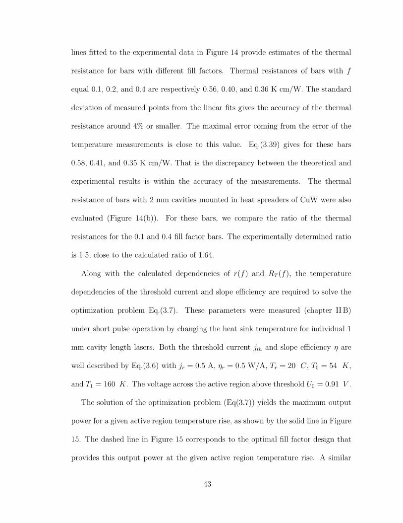
The solution of the optimization problem (Eq(3.7)) yields the maximum output
power for a given active region temperature rise, as shown by the solid line in Figure
15. The dashed line in Figure 15 corresponds to the optimal fill factor design that
provides this output power at the given active region temperature rise. A similar
43
FIG. 14: Measured overheating of the active region versus dissipated power density pdis (a)
for different fill factor laser bars with 1 mm long cavities mounted in BeO heat spreaders
and (b) for different fill factor laser bars with 2 mm long cavities mounted in CuW heat
spreaders. Solid symbols indicate data points (circles, squares, and triangles for 10%, 20%,
and 40% fill factors respectively). Lines fit to the experimental data are used to determine
the thermal resistance.
44
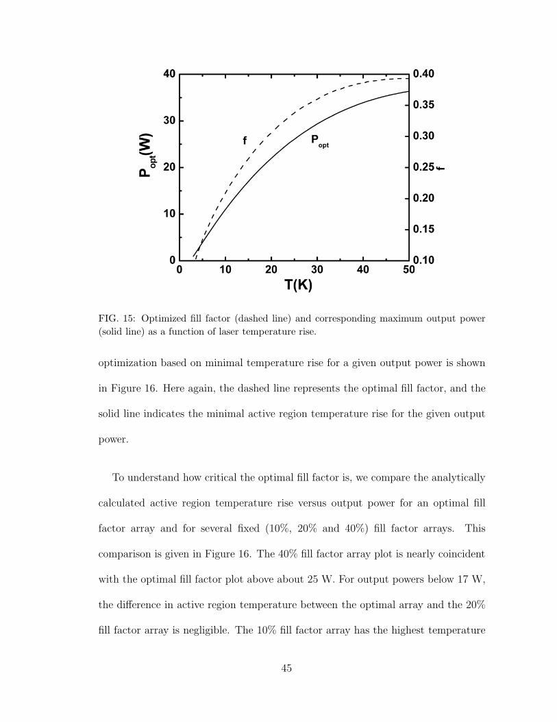
FIG. 15: Optimized fill factor (dashed line) and corresponding maximum output power
(solid line) as a function of laser temperature rise.
optimization based on minimal temperature rise for a given output power is shown
in Figure 16. Here again, the dashed line represents the optimal fill factor, and the
solid line indicates the minimal active region temperature rise for the given output
power.
To understand how critical the optimal fill factor is, we compare the analytically
calculated active region temperature rise versus output power for an optimal fill
factor array and for several fixed (10%, 20% and 40%) fill factor arrays. This
comparison is given in Figure 16. The 40% fill factor array plot is nearly coincident
with the optimal fill factor plot above about 25 W. For output powers below 17 W,
the difference in active region temperature between the optimal array and the 20%
fill factor array is negligible. The 10% fill factor array has the highest temperature
45

FIG. 16: Optimized fill factor (dashed line) and corresponding minimal laser temperature
rise (solid line) as a function of output power. The dotted lines show the temperature rise
for several fixed fill factor arrays as a function of output power.
among the rest arrays above 5W. Clearly, the optimal fill factor depends on the bar
operating regime.
Earlier we suggested two methods of increasing array output power: increasing
the pumping current per emitter and increasing the number of emitters. By calcu-
lating the optimal fill factor for a particular operating regime, we have found the
most favorable balance between these two approaches. The optimal fill factor curve
shown in Figure 15 illustrates that for increasing output power in this system, it is
preferable to use a higher fill factor. Higher fill factors offer advantages for higher
power operation since the effect of mutual heating is weaker than the heating of
each one of them by the current.
46
F. Conclusion
In this chapter
• We obtained analytical expressions for the steady state electrical and ther-
mal resistance of a laser bar. Both quantities depend on geometry, and in
particular, the fill factor.
• Theoretical results for the thermal resistance are in excellent agreement with
the measured thermal resistance of 1 and 2 mm cavity length laser arrays with
different fill factors.
• We use the analytical results to calculate the optimal laser bar fill factor. The
value of the optimal fill factor depends on the working regime of the bar;
higher output powers require higher fill factors for minimum active region
temperatures.
47

IV. PERFORMANCE OF INFRARED HIGH-POWER LASER DIODE
ARRAYS
A. Introduction
Replacing flash-lamps with efficient, narrow-band diode laser pumping sources
significantly increased the maximum available power and extended the application
area of solid-state lasers. In recent years, there has been an increased interest in
the development of high-energy, Q-switched solid-state sources operating in eye-safe
wavelength range. Optically pumped erbium-doped crystalline hosts offer great po-
tential as efficient, pulsed, eye-safe laser sources. The further progress of Er:doped
solid state laser is determined by the development of high-power laser arrays reli-
ably delivering energy in Er absorption bands near 1.5-µm. High-power electrically
pumped semiconductor laser arrays operating near 2.3-µm can be used for optical
pumping of recently developed type-II semiconductor lasers [37].
This chapter describes the design and performance of infrared laser diode arrays.
It is organized as follow. In section IVB we consider the details of design and
performance of high-power laser arrays fabricated for optical pumping of Er:YAG
solid-state lasers. The operation of 2.3-µm laser arrays is discussed in section IVC.
The steady-state thermal analysis of high-power laser diode arrays is considered in
the section IVD.
48

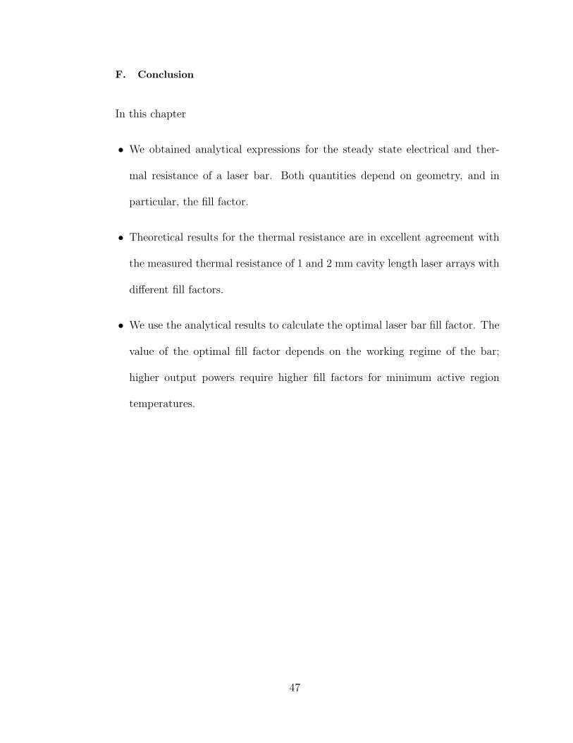
B. Design and performance of 1.5-µm laser arrays
The laser arrays operating at 1.5-µm were fabricated from InGaAsP/InP wafer
grown by organometallic chemical vapor deposition. The laser active region con-
sisted of three 6-nm-thick compressively strained quantum wells incorporated into a
two-step graded index waveguide with a total thickness of 710 nm. The laser facets
were high-reflection/anti-reflection coated with reflection coefficients of 95% and 3%,
respectively. Single 100-µm-wide, 1-mm-long lasers demonstrated a threshold cur-
rent density of 480 A/cm2 and a differential efficiency of 60%. Over the temperature
range from 18 to 60 oC, the threshold characteristic temperature T0 was 54 oK and
the slope-efficiency characteristic temperature T1 was 160 oK. The performance of
single emitters is described in details in section IIB.
Based on the characterization results of single emitter performance (chapter IIB)
and the solution for laser bar design optimization (chapter III), we chose the design
of laser diode bar. We used 1-cm-long laser bars containing twenty 100-µm-wide
emitters equally spaced over 10 mm laser bar with 500 µm center-to-center distance,
yielding a fill factor of 20%. The laser cavities were 1 mm long to fit the standard
heat sink assembly. One-dimensional (1D) and two-dimensional (2D) arrays were
fabricated by mounting one bar or multiple bars in metallized grooves in BeO blocks
(heatspreaders), which were bonded on water-cooled microchannel heat sinks. This
arrangement removes heat from both sides of the laser bar.
Figure 17 shows the current dependencies of the cw and q-cw (5-ms pulse dura-
tion, 20-Hz pulse repetition frequency) output power and the wall-plug efficiency for
49
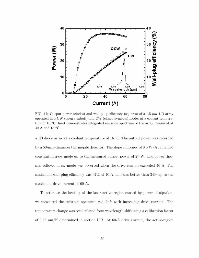
FIG. 17: Output power (circles) and wall-plug efficiency (squares) of a 1.5-µm 1-D array
operated in q-CW (open symbols) and CW (closed symbols) modes at a coolant tempera-
ture of 16 oC. Inset demonstrates integrated emission spectrum of the array measured at
40 A and 18 oC.
a 1D diode array at a coolant temperature of 16 oC. The output power was recorded
by a 50-mm-diameter thermopile detector. The slope efficiency of 0.5 W/A remained
constant in q-cw mode up to the measured output power of 27 W. The power ther-
mal rollover in cw mode was observed when the drive current exceeded 40 A. The
maximum wall-plug efficiency was 37% at 40 A, and was better than 34% up to the
maximum drive current of 60 A.
To estimate the heating of the laser active region caused by power dissipation,
we measured the emission spectrum red-shift with increasing drive current. The
temperature change was recalculated from wavelength shift using a calibration factor
of 0.55 nm/K determined in section IIB. At 60-A drive current, the active-region
50

temperature rise was 18 oK in the cw mode and 13 oK in the q-cw mode. The
thermally induced rollover of cw output power appeared in LI-characteristics at
active region temperature of 28 oC.
The inset of Figure 17 shows the integrated emission spectrum of the 1D array
measured at an 18 oC coolant temperature. The full-width at half-maximum of the
emission spectrum of 1D laser array was about 8 nm.
A 2D laser array consisted of series connected four bars with a bar-to-bar pitch
of 3.2 mm. Each bar had twenty 100 µm wide emitters equally distributed over 1
cm laser bar. A q-cw output power of 110 W was achieved at a current of 60 A, as
shown in Figure 18. The 2D array integrated emission spectra were measured at a
current of 30 A in q-cw mode at 18 and at 25 oC as shown in the inset in Figure
18. The spectrum shifted with temperature, while the full width at half maximum
spectral width remained at about 10 nm.
C. Design and performance of 2.3-µm laser arrays
The laser heterostructure was grown by solid source molecular-beam epitaxy on
n-GaSb substrates. The device consisted of a 800-nm-thick Al0.25Ga0.75As0.02Sb0.98
broadened-waveguide layer consisting of two QWs sandwiched between 2-µm-thick
Al0.9Ga0.1As0.07Sb0.93 cladding layers. The details of single laser characterization
and design are discussed in the chapter IIC and [21, 22, 25]. Based on the charac-
terization of single emitter devices (chapter IIC), we determined an optimal(chapter
III) laser bar design for cw and qcw operations.
A 1-cm-wide 1-mm-long anti-reflection/high-reflection coated laser bar containing
51
FIG. 18: Output power of a 2-D array operated in the q-cw mode at 18 oC. Inset demon-
strates integrated emission spectrum of a 2-D array recorded at 40 A and 18 oC.
19 100-µm-wide emitters separated by 500 µm was soldered into a microchannel-
cooled BeO heat sink. Figure 19 shows its light-current characteristics and wall-plug
efficiency, as well as its spectrum (insert) at 30 A cw, all measured at 18 C. The
maximum CW power of 10 W is reached at 70 A. The spectrum is centered near
2.36-µm with a FWHM of about 20 nm at 30-A cw. In the qCW mode (30 µs, 300
Hz, 0.9% duty cycle) the array output over 18.5-W peak power at a peak current
of 100 A. In the short-pulse, low-duty-cycle mode, the light-current characteristics
is linear up to nearly 20 W of peak power at 100 A of peak current without any
cooling.
Array heating causes saturation of the cw and qcw light-current characteristics.
The thermal resistance of the array with 20% fill factor is about 0.4 K/W and
52

FIG. 19: Current characteristics of output-power and wall-plug efficiency of 2.3-µm laser
linear array. The light-current characteristics in cw and q-cw were measured at 18 oC
coolant temperature and at room temperature (uncooled) in short pulse operation. The
inset shows the laser array emission spectrum measured at 30-A drive current and 18 oC
coolant temperature in CW operation.
was determined from the emission spectrum red shift with power dissipation. This
result is in good agreement with analytically calculated one in the chapter IIID.
This thermal resistance leads to active region overheating of about 25 oK at an
output power of 5-W cw and about 75 oK at 10 W. The somewhat excessive heating
at high currents is related to the wall-plug efficiency (9% maximum). The array cw
output power could be increased substantially if the wall-plug efficiency is improved.
The relatively low laser power conversion efficiency is attributed to 1) 50% inter-
nal efficiency about 50% of the injection current after threshold is parasitic, and 2)
excess voltage drop across the laser heterostructurethe voltage at threshold is about
53

1 V and it rises up to over 2 V at 3 A for a single laser, while laser energy quantum
is only 0.54 eV.
The internal efficiency is reduced by lateral current spreading and nonradiative
Shockley - Reed - Hall recombination in the waveguide layer [67, 68]. Lateral cur-
rent spreading is substantial in the current laser design since no steps were taken
to confine carriers laterally at the time of wafer processing [67]. Lateral current
spreading can be expected in the 2-µm p-cladding and 800-nm waveguide layers as
well as from lateral diffusion in the QWs [68].
The parasitic barriers for carrier transport from cladding to waveguide layer
makes a large contribution to the excessive voltage drop and series resistance [69].
Careful adjustment of the cladding/waveguide material composition and doping
profile can reduce the excessive voltage drop across the laser heterostructure.
Once the laser power conversion efficiency is improved, the optimum laser bar
fill-factor will be higher than the current 20%, thus increasing the maximum power
from a single bar.
D. Steady-state thermal analysis of high-power laser arrays
The limited wall-plug efficiency of high power laser arrays leads to a considerable
amount of heat generated under high power steady state operation. To reduce array
overheating, the common approach is to increase the area through which the heat is
dissipated (thermal foot print). The thermal foot print can be enlarged by extending
the cavity length, or increasing the number of emitters. For the array architecture
of Figure 13, a cavity length increase requires thicker heat spreader blocks. The
54
thicker heat spreader leads to a longer heat propagation length towards the heat
sink and higher thermal gradient along the cavity length [43, 70]. The electrically
pumped active region area of the laser bar can be efficiently increased by reducing
the distance between adjacent stripes of constant width (i.e. by increasing the fill
factor). However, decreasing the separation between adjacent emitters can lead to
increased mutual heating. The effect of fill factor on overheating is considered in
this section.
The temperature of the active region is a critical factor in the operational lifetime
of the array. Previous results indicate that the lifetime is exponentially dependent
on the active region temperature [71, 72]. The main factors determining the tem-
perature of the active region are the power dissipation in the active area, the series
resistance of the cladding layers, and the mutual heating of adjacent emitters.
To study the influence of laser bar design on overheating, we fabricated InP-based
arrays with fill factors of 10%, 20% and 40% and measured the dependence of the
active region temperature change on dissipated power (Pdis), which is defined as the
difference between input electrical power and output optical power. The overheating
of the laser active region was obtained by measuring the emission spectrum red-shift.
As can be seen in the Figure 20, the active-region temperature depends linearly on
dissipated power with the thermal resistance as the coefficient of proportionality.
The thermal resistances of 0.56, 0.4, and 0.34 K/W were experimentally determined
for 10%, 20% and 40% fill factor arrays, respectively. The thermal resistance was
found to be significantly decreased by increasing fill factor from 10% to 20% and
changed much less with further fill factor increases. The inset shows this decreasing
55

FIG. 20: The experimentally measured active-region temperature rise as a function of
dissipated power is shown for different fill factor arrays. The inset shows the dependence
of the thermal resistance on fill factor.
dependence of thermal resistance on fill factor, which saturates at high FF, in good
agreement with Ref. [73].
This dependence of the thermal resistance on the fill factor results from a nonuni-
form temperature distribution in the laser bar. To clarify the experimental results,
we developed an analytical model (chapter IIID) based on the solution of the heat
conduction equation with non-trivial boundary conditions defined by the geometry
of laser array. In this thermal model, we simulated the real geometry (Figure 13b)
with a structure in which the laser bar, the BeO layer, and the ideal heat sink are
coplanar (Figure 13a). The 830-mm thickness of the BeO layer was determined by
56
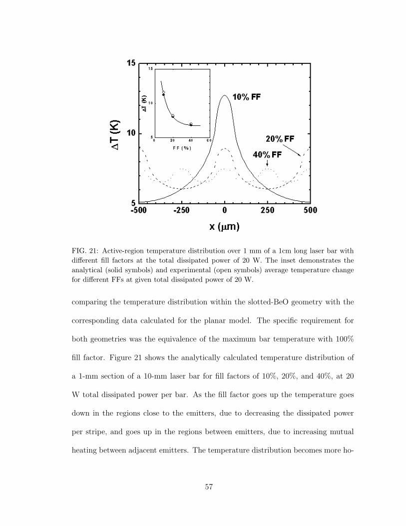
FIG. 21: Active-region temperature distribution over 1 mm of a 1cm long laser bar with
different fill factors at the total dissipated power of 20 W. The inset demonstrates the
analytical (solid symbols) and experimental (open symbols) average temperature change
for different FFs at given total dissipated power of 20 W.
comparing the temperature distribution within the slotted-BeO geometry with the
corresponding data calculated for the planar model. The specific requirement for
both geometries was the equivalence of the maximum bar temperature with 100%
fill factor. Figure 21 shows the analytically calculated temperature distribution of
a 1-mm section of a 10-mm laser bar for fill factors of 10%, 20%, and 40%, at 20
W total dissipated power per bar. As the fill factor goes up the temperature goes
down in the regions close to the emitters, due to decreasing the dissipated power
per stripe, and goes up in the regions between emitters, due to increasing mutual
heating between adjacent emitters. The temperature distribution becomes more ho-
57
mogenous along the bar with increasing FF, reducing the influence of fill factor on
the thermal resistance. In the inset of Figure 21 we compared the analytic results
for average active region temperature rise versus fill factor with the experimental
results, and found good agreement. In agreement with experimental results, our
calculations show that a further fill-factor increase (f > 40%) does not lead to
significant reduction of overheating.
E. Conclusion
In this chapter
• We report on the development of high-power diode arrays operating near 1.5
µm. A 25-W cw output power was obtained from a 1D array at 16 oC, and
110-W qcw power was obtained from a 2D array at 18 oC.
• Diode laser linear arrays emitting at 2.3-µm output 10-W cw and 18.5-W qcw
(30µs/300 Hz). The array peak wall-plug efficiency was near 9%.
• In steady-state operation the thermal resistance decreases with increased fill
factor; however, this dependency saturates at high FFs. The good agreement
between the theoretical and experimental results shows that the analytical
model developed in the chapter IIID is adequate to determine the temperature
distribution in the laser arrays.
58

V. TRANSIENT THERMAL ANALYSIS OF HIGH-POWER DIODE
LASER ARRAYS WITH DIFFERENT FILL FACTORS
A. Introduction
The high heat dissipation in the laser arrays makes effective thermal management
a critical issue for reliable and efficient operation. In section IVB we considered
the InP-based laser arrays designed for resonant pumping of erbium doped solid
state lasers [43]. The optical pumping scheme requires high power sources that
can reliably provide a large fraction of their output energy in relatively narrow
erbium absorption bands. The erbium fluorescence lifetime of about 5-10 ms favors
relatively long pump-laser pulses [15–17]. The long current-injection pulses produce
a considerable temperature increase within the diode laser structure that induces
a red-shift of the output wavelength. The thermal drift of laser array emission
spectra can lead to misalignment with erbium absorption bands. Pump-laser power
falling outside these bands cannot be absorbed and is wasted, deteriorating the
pumping efficiency. The reliability of pumping arrays is one more important issue
for solid state laser systems. Laser array degradation mechanisms are enhanced
by high operational temperatures, and aging tests indicate that the laser array
lifetime decreases exponentially with active region temperature [72]. Another key
parameter for optically pumped solid state laser systems is the output power of the
pumping diodes, which is known to saturate with temperature. In recent years,
many groups optimized the design of laser arrays to decrease the thermal load and
maximize the output power in different operating regimes [6, 77, 83]. It was shown
59
that arrays with high emitter density (large fill factor) are preferred for short-pulse
high peak power operation [5, 84], while arrays with low emitter density (small
fill factor) are better suited for long-pulse, high average power operation [11, 12].
For efficient near-resonant pumping of erbium solid-state lasers the design of the
laser bars and package architecture should minimize the active-region temperature
rise, and hence, minimize the pump-laser spectral red-shift throughout the long-
pulse duration. A comprehensive thermal analysis of the packaged laser arrays
provides a powerful tool for the design optimization. The steady-state temperature
distributions in semiconductor laser diodes were evaluated from numerical [13] and
analytical [49, 85, 86] solutions of the heat conductance equation with different
boundary conditions. In section IVD and [43, 70] the temperature distribution was
obtained for laser diode bars in cw mode operation. The transient thermal response
of high power LDAs was studied experimentally [62, 71] and theoretically [70, 73]
for laser bars with planar heat spreaders. In this chapter we consider the effect of
laser bar design on transient temperature change for laser bars mounted in bar-in-
groove heat spreaders. A good agreement between the theoretical modeling and the
experimental results was demonstrated.
In section VB, the laser bar design and the heating kinetics measurements are
discussed. The description of theoretical model is presented in section VC. Section
VD discusses the experimental results and their comparison with the analytical
model.
60
B. Device structure and experimental technique
The InGaAsP/InP laser structure emitting at 1.5-µm was grown by metalloor-
ganic chemical vapor deposition. The active region contains three InGaAsP quan-
tum wells (QWs). The broadened waveguide (710 nm) was incorporated between
n- and p-clad layers, each 1.5-µm thick. The total thickness of the laser bar struc-
ture including the substrate was 140 µm. The 100-µm-wide, 1-mm-long laser stripes
were equally spaced along the 1-cm-wide laser bar and were separated by unpumped
regions. The laser bars with 10%, 20%, and 40% fill factors (FF) were fabricated.
These bars were mounted onto metallized grooves in 2-mm-thick BeO heat spreaders
bonded to water-cooled microchannel heat sinks; see the the Figure 13. Details of
the laser heterostructure and bar design were considered in chapters IVB and IIB
and in Ref.[43, 44]. The laser diode arrays with different FFs showed a threshold
current density of 480 A/cm2 and a slope efficiency of 0.5 W/A in the linear part of
the light-current characteristic at room temperature.
The temperature kinetics in the active region was determined by measuring the
temporal evolution of the laser spectra during a 400-ms current pulse. The pulse
duration was chosen to be long enough to reach a steady-state operation regime. The
spectrum evolution was measured using a 0.5-m grating monochromator equipped
with a linear 256-pixel InGaAs photodetector. The photodetector array captured the
laser array spectrum with a resolution of 0.16 nm without rotating the diffraction
grating. The total full-width at half-maximum (FWHM) spectral width for the
arrays was typically around 10 - 15 nm, while single emitters cleaved from the same
61
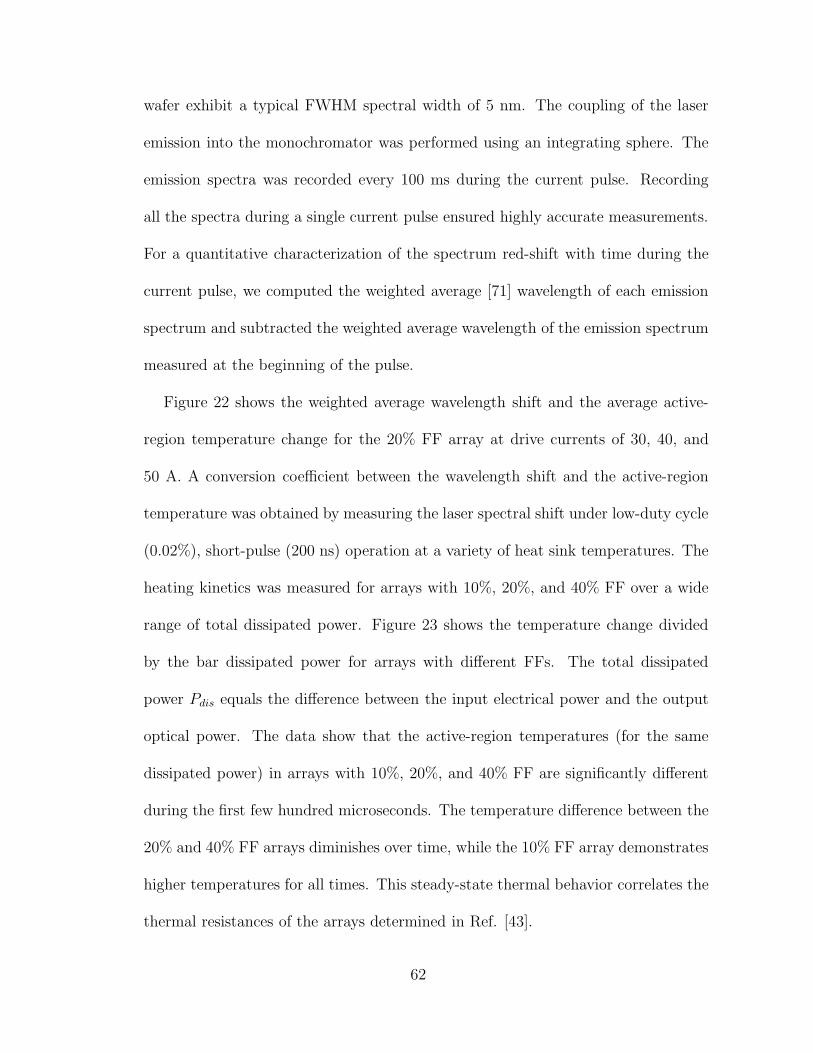
wafer exhibit a typical FWHM spectral width of 5 nm. The coupling of the laser
emission into the monochromator was performed using an integrating sphere. The
emission spectra was recorded every 100 ms during the current pulse. Recording
all the spectra during a single current pulse ensured highly accurate measurements.
For a quantitative characterization of the spectrum red-shift with time during the
current pulse, we computed the weighted average [71] wavelength of each emission
spectrum and subtracted the weighted average wavelength of the emission spectrum
measured at the beginning of the pulse.
Figure 22 shows the weighted average wavelength shift and the average active-
region temperature change for the 20% FF array at drive currents of 30, 40, and
50 A. A conversion coefficient between the wavelength shift and the active-region
temperature was obtained by measuring the laser spectral shift under low-duty cycle
(0.02%), short-pulse (200 ns) operation at a variety of heat sink temperatures. The
heating kinetics was measured for arrays with 10%, 20%, and 40% FF over a wide
range of total dissipated power. Figure 23 shows the temperature change divided
by the bar dissipated power for arrays with different FFs. The total dissipated
power Pdis equals the difference between the input electrical power and the output
optical power. The data show that the active-region temperatures (for the same
dissipated power) in arrays with 10%, 20%, and 40% FF are significantly different
during the first few hundred microseconds. The temperature difference between the
20% and 40% FF arrays diminishes over time, while the 10% FF array demonstrates
higher temperatures for all times. This steady-state thermal behavior correlates the
thermal resistances of the arrays determined in Ref. [43].
62

FIG. 22: Time dependence of average wavelength shift (left axis) and the corresponding
active region temperature change (right axis) for a laser diode array with a 20% fill factor.
C. Theory
1. Vertical geometric model
To describe the transient active-region thermal behavior of laser arrays, we de-
veloped an analytical model including the main features of the laser array assembly.
The schematic cross section of the array assembly considered in the model is shown
in Figure 24.
The BeO heat spreader occupies the region 0 < y < b and isothermally contacts
an ideal heat sink at y = b. The bottom edge (y = 0) of the heat spreader is
adiabatically isolated. The thickness of the heat spreader is at least one order of
63

FIG. 23: Active region temperature rise divided by dissipated power (i.e. thermal resis-
tance) as a function of time for different FF arrays.
magnitude larger than the thickness of the laser bar. Because of this, we neglect the
thickness of the laser bar, which can be represented by a homogeneous heat source
located at x = 0, 0 < y < a and shown in Figure 24 by the line AB. The heat
conductance problem is reduced to the solution of the equation
∂T
∂t= χ
(
∂2T
∂x2+∂2T
∂y2
)
, (5.1)
in the region x > 0, 0 < y < b with boundary conditions
κ∂T
∂y
∣
∣
∣
∣
y=0
= 0 , (5.2a)
κ∂T
∂x
∣
∣
∣
∣
x=0
= −Qθ(a − y) , a < b , (5.2b)
T |y=b = 0 , (5.2c)
64

FIG. 24: The cross section geometry of the laser array assembly used for the calculation
of the temperature distribution is shown. The BeO heat spreader occupies the region
0 < y < b. The laser bar is plotted by the line A-B. The interface between the BeO heat
spreader and the heat sink lies at y = b.
and the initial condition
T |t=0 = 0 . (5.3)
where T is the temperature change due to heating, χ and κ are the BeO thermal
diffusivity and conductivity, respectively, and Q is the heat flux density from the
laser structure. Due to the symmetry of the problem, we consider only the region
x > 0. The equation is solved using the Laplace transformation. The equation is
solved using the Laplace transformation (Appendix VF), and the result is after the
inverse Laplace transformation
T (x, y, t) =4Q
√χ
πκ
∞∑
n=0
1
2n+ 1sin
π(2n+ 1)a
2bcos
π(2n+ 1)y
2b
× 1
2πi
∫ δ+i∞
δ−i∞
exp[
pt− x√
p+ (2n+ 1)2/τ/√χ]
p√
p+ (2n+ 1)2/τdp(5.4)
65
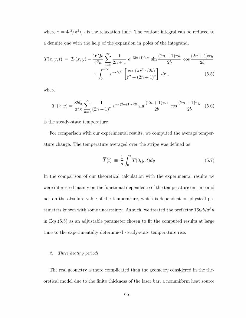
where τ = 4b2/π2χ - is the relaxation time. The contour integral can be reduced to
a definite one with the help of the expansion in poles of the integrand,
T (x, y, t) = T0(x, y) −16Qb
π3κ
∞∑
n=0
1
2n+ 1e−(2n+1)2t/τ sin
(2n+ 1)πa
2bcos
(2n+ 1)πy
2b
×∫
−∞
0
e−r2t/τ
[
cos (πr2x/2b)
r2 + (2n+ 1)2
]
dr , (5.5)
where
T0(x, y) =8bQ
π2κ
∞∑
n=0
1
(2n+ 1)2e−π(2n+1)x/2b sin
(2n+ 1)πa
2bcos
(2n+ 1)πy
2b(5.6)
is the steady-state temperature.
For comparison with our experimental results, we computed the average temper-
ature change. The temperature averaged over the stripe was defined as
T (t) ≡ 1
a
∫ a
0
T (0, y, t)dy (5.7)
In the comparison of our theoretical calculation with the experimental results we
were interested mainly on the functional dependence of the temperature on time and
not on the absolute value of the temperature, which is dependent on physical pa-
rameters known with some uncertainty. As such, we treated the prefactor 16Qb/π3κ
in Eqs.(5.5) as an adjustable parameter chosen to fit the computed results at large
time to the experimentally determined steady-state temperature rise.
2. Three heating periods
The real geometry is more complicated than the geometry considered in the the-
oretical model due to the finite thickness of the laser bar, a nonuniform heat source
66
distribution in the bar, and the nonideality of the water-cooled heat sink. The first
two factors are important in the short-time scale and the last one affects the es-
timation of the relaxation time τ , which describes longer-time-scale heating. The
heating of the laser bar structure controls the initial active-region temperature rise.
The heat is generated in the active regions under the metal stripe contacts and
produces heat fluxes. The propagation of heat fluxes from the InP-based laser bar
structure to the BeO heat spreader is hindered by the In-based solder layer serving
as interface between these materials and the smaller value of thermal diffusivity of
InP (χ1 = 0.37 cm2/s) in comparison with BeO (χ = 0.9cm2/s). During the initial
period of heating, lateral heat spreading and heating of the laser bar occurs. The
duration of this period τ1 can be estimated as l21/χ1, where l1 ∼ 100µm is a char-
acteristic length on the order of the thickness of the laser bars and the separation
between adjacent stripes in the laser bar. The initial heating of the laser bar struc-
ture was included in our model by assuming that the measurement starts with time
delay t0 ≈ τ1 after the beginning of the current pulse. The analytically calculated
heating kinetics is shown by the dashed lines in Figure 22 for the 30-, 40-, and 50-A
drive currents.
The analytical model describes the heating at t > τ1 after the entire laser bar has
been heated and the nonuniformity of the heat source distribution is diminished. In
this time range (t > τ1) it is possible to separate two periods when the temperature
kinetics given by Eqs.(5.5) can be greatly simplified. In the short-time kinetics
t << τ , i.e., the second period of heating, a simplified form of the solution can be
obtained directly from Eqs.(5.28) and (5.7), where the condition t << τ corresponds
67

FIG. 25: The Active-region initial temperature rise during the first 200 mus for 10%,
20%, and 40% FF arrays at a constant total bar Pdis of 25 W.
to pt >> 1. This gives
T (t) =2Q
√χt
κ√π
(5.8)
The third period of heating is the long-time kinetics when t >> τ . In this period,
the rapid decay of the exponential terms make it possible to approximate the tem-
perature change using just one term (n = 0) from the sum obtained by substituting
Eq.(5.5) and (5.7).
T (t) = T0
(
1 −√
τ
πts−t/τ
)
, (5.9)
where
T0 =8bQ
π2κ
2b
πasin2
(πa
2b
)
(5.10)
68

In summary, the heating process can be subdivided into three time periods, each
with different heat transport conditions. During the first period, the active-region
temperature increase of laser arrays is determined by heating the structure very close
to the laser stripes. As the first period progresses, the heat fluxes from individual
laser stripes overlap, producing a nearly uniform heat flux. In the second period
the unified heat flux propagates through the BeO heat spreader toward the cooler,
but the substantially heated region is still much smaller than the thickness of the
heat spreader. The heating kinetics is determined by Eq.(5.8) and the temperature
change of the active region is proportional to the square-root of time. In the third
period the heat flux has reached the heat sink, the entire BeO heat spreader is
heated, and the active-region temperature asymptotically approaches its steady-
state value, Eq.(5.9).
D. Results and discussion
To study the initial heating (t ≤ τ1) of laser arrays with different fill factors, the
active-region temperature rise sDT1d was measured for the first 200 µs. Figure 25
demonstrates the dependence of T1 on FF at 25-W total dissipated power per bar.
The experimental results show that the temperature rise during the first 200 µs is
highest for the array with a 10% FF and smallest for the array with 40% FF. In
the first heating period the active-region heating is mainly determined by the power
dissipation in each stripe. The dissipated power per stripe scales with the number
of stripes for a constant total dissipated power in the bars. At a given dissipated
power in the bar, the temperature rise decreases with the fill factor. This decrease
69

FIG. 26: The temperature changes are plotted on double-log axes for the three fill factors.
The solid lines were fitted to the experimental data over the time interval of 200 µs to 10
ms. The computed slopes are shown in the inset as a function of the fill factor.
is not directly proportional to the number of stripes. During the first 200 µs, the
active-region temperature increases are 9 K for 10% FF, 6.5 K for 20% FF, and 4.5 K
for 40% FF at 25-W dissipated power per bar. This is an evidence of the lateral heat
transport in the laser bar structure that is responsible for the mutual heating of the
adjacent emitters. This lateral heat transport leads to an overlapping of heat fluxes
from the active-region areas under the metal contacts and to the homogenization of
the temperature distribution in the laser bar.
The second period lasts while τ1 < t ≪ τ ends before the heat flux reaches
the heat sink. Since in the first period the heat fluxes from under the stripe areas
70

FIG. 27: The active-region temperature change of a 20% fill factor array is plotted vs the
square-root of time with 30-, 40-, and 50-A drive currents at a coolant temperature of 18oC. The dependency of the slope coefficient α the total dissipated power is shown for 10%
(square symbol), 20% (circle symbol), and 40% (triangle symbol) fill factor arrays in the
inset.
have merged into a nearly uniform flux, the thermal kinetics is expected to be
independent of the distance between emitters (i.e., fill factor) in this second phase
of heating. To analyze the active-region temperature change during the second
period, the initial temperature rise (T1) was subtracted from the measured active-
region temperature. Figure 26 shows the temperature change on double-log axes for
arrays with the three different fill factors. The solid lines in Figure 26 were fitted to
the experimental data over the time interval from 200 µs to about 10 ms. The inset
shows the computed slopes as a function of the fill factor. The slope of these fit
lines is close to 0.5, indicating that the active-region temperature change increases
71
as the square-root of time. Figure 27 shows the active-region temperature change
versus the square-root of time for a 20% fill factor array at 30-, 40-, and 50-A drive
currents, which corresponds to 21.5-, 29-, and 38.5-W total dissipated power. The
temperature dependencies are well approximated by straight lines with the slope
coefficient a. The measured slope coefficients have been plotted in the inset for
10%, 20%, and 40% FF arrays as functions of the total dissipated power. The slope
coefficient increases linearly with the total dissipated power at the same rate for
all three arrays. This shows that over the time scale τ1 < t ≪ τ the temperature
kinetics is determined by the free propagation of the nearly uniform heat flux in the
BeO heat spreader and does not depend on the fill factor. This thermal behavior is
well described by the asymptotic analytical solution of Eq.(5.8).
In the third period (t≫ τ), the active-region temperature change approaches the
steady-state value (T0) with a characteristic time constant τ and is characterized by
long-time asymptotic kinetics given by Eq.(5.9). Equation (5.9) can be rewritten as
[T0 − T (t)]
T0
=
√
τ
πtexp(−t/τ). (5.11)
For t≫ τ , the exponential time dependence dominates the preceding term√
τ/πt,
and Eq. (5.11) can be simplified as
[T0 − T (t)]
T0∼ exp(−t/τ). (5.12)
In Figure 28 the normalized difference between the active-region temperature change
and the experimentally determined steady-state temperature rise (T0) is plotted
in semilogarithmic scale for all three arrays. Figure 5 shows that for long times,
t > 20ms, the data are well approximated by the exponential time dependence
72

FIG. 28: Normalized deviation from steady-state temperature vs time is plotted for arrays
with 10%, 20%, and 40% FF. The slopes of the solid lines are used to calculate τc, which
is shown in the inset.
given by Eq.5.12). The slopes of the solid lines in Figure 28 were fitted to the
data to calculate the experimental time constant τc, which is shown in the inset
as a function of FF. The long-time heating kinetics of these arrays with different
FFs can be characterized with the same τc of about 60 ms. The experimental time
constant τc is larger than the theoretically calculated time constant, τ ≈ 20ms.
The reason for the discrepancy is that the theoretical model describes only the
heat propagation through the heat spreader, while in reality there are other factors
affecting the temperature kinetics, such as the nonideality of the water-cooled heat
sink and the interface between the BeO heat spreader and the heat sink.
73

E. Conclusion
In this chapter
• We report on the experimental and theoretical study of heating kinetics for
InGaAsP/InP arrays with 10%, 20%, and 40% fill factors. The transient heat-
ing process can be divided into three time periods; each period is determined
by its own heat transport condition. During the first period, the bar structure
is heated and the heat fluxes from individual stripes of the laser bar overlap,
producing the nearly uniform heat flux. The duration of this period s (τ1) is
determined by the geometry of the laser bar and its thermal diffusivity. The
second period is characterized by the propagation of the nearly uniform heat
flux through the BeO heat spreader. The heat propagation length for the
second period is much smaller than the heat spreader thickness. By the third
period the heat flux has reached the heat sink, the entire heat spreader has
been heated, and the temperature distribution approaches the steady state.
• The theoretical model describes the heating in the second and the third heat-
ing periods. In the second period the active-region temperature change of
laser arrays is proportional to the square-root of time, and in the third period
the deviation of the temperature from its steady-state value decreases expo-
nentially with time. The initial temperature rise is included in the model by
assuming a time delay (t0 ≈ τ1) to heat the laser bar structure.
• The temperature rise measured for the first 200 µs is dependent on the power
dissipated per stripe and the distance between stripes. This initial tempera-
74
ture change decreases with the fill factor for a given total bar power dissipation
and bar size. The second and third periods are well described by the asymp-
totic solutions of the theoretical model. The maximal difference between the
analytically predicted temperature and the experimental one is about two de-
grees for the largest current, 50 A. This small difference indicates that our
model adequately describes the array heating process. The discrepancy be-
tween the theoretical and experimental values of the time constant t in the
third heating period shows that the thermal properties of the interfaces and
the nonideality of the heat sink substantially affect the heat flow.
75
F. Appendix (Vertical geometric model)
The problem is to solve the equation
∂T
∂t= χ
(
∂2T
∂x2+∂2T
∂y2
)
, (5.13)
in the region x > 0, 0 < y < b with boundary conditions
κ∂T
∂y
∣
∣
∣
∣
y=0
= 0 , (5.14a)
κ∂T
∂x
∣
∣
∣
∣
x=0
= −Qθ(a − y) , a < b , (5.14b)
T |y=b = 0 , (5.14c)
and the initial condition
T |t=0 = 0 . (5.15)
After the Laplace transform,
Θ(x, y) =
∫
∞
0
e−ptT (x, y, t)dt , (5.16)
the problem is reduced to the equation
χ
(
∂2Θ
∂x2+∂2Θ
∂y2
)
= pΘ , (5.17)
with boundary conditions
κ∂Θ
∂y
∣
∣
∣
∣
y=0
= 0 , (5.18a)
κ∂Θ
∂x
∣
∣
∣
∣
x=0
= −Qpθ(a− y) , a < b , (5.18b)
Θ|y=b = 0 , (5.18c)
76
The problem Eqs.(5.17) and (5.18) is equivalent to
∂2Θ
∂x2+∂2Θ
∂y2− p
χΘ = 0 , (5.19)
in the stripe −b < y < b with the boundary conditions
Θ(x,±b) = 0 , κ∂Θ
∂x
∣
∣
∣
∣
x=0
= −Qpθ(a− |y|) (5.20)
The solution can be represented in the form
Θ(x, y) =
∞∑
n=0
Θn(x) cosπ(2n+ 1)y
2b. (5.21)
Then
Θn(x) =1
b
∫ b
−b
Θ(x, y) cosπ(2n+ 1)y
2bdy , (5.22)
that leads to the equation
d2Θn
dx2−
[
p
χ+π2(2n+ 1)2
4b2
]
Θn = 0 (5.23)
with the boundary condition
dΘ
dx
∣
∣
∣
∣
x=0
= − Q
κp
4
π(2n+ 1)sin
π(2n+ 1)a
2b. (5.24)
The solution to this equation that goes to zero at x→ ∞ is
Θn(x) =Q
κp
4
π(2n+ 1)sin
π(2n+ 1)a
2b
[
p
χ+π2(2n+ 1)2
4b2
]−1/2
× exp
−[
p
χ+π2(2n+ 1)2
4b2
]1/2
x
. (5.25)
The substitution in Eq.(5.21) gives
Θ(x, y) =4Q
√χ
πκp
∞∑
n=0
exp[
−x√
p+ (2n+ 1)2/τ/√χ]
(2n+ 1)√
p+ (2n+ 1)2/τsin
π(2n+ 1)a
2b
× cosπ(2n+ 1)y
2b, (5.26)
77

where
1
τ=π2χ
4b2. (5.27)
After the inverse Laplace transformation
T (x, y, t) =4Q
√χ
πκ
∞∑
n=0
1
2n + 1sin
π(2n+ 1)a
2bcos
π(2n+ 1)y
2b
× 1
2πi
∫
L
exp[
pt− x√
p+ (2n+ 1)2/τ/√χ]
p√
p + (2n+ 1)2/τdp
= T0(x, y) +4Q
√χ
πκ
∞∑
n=0
1
2n + 1e−(2n+1)2t/τ sin
π(2n+ 1)a
2bcos
π(2n+ 1)y
2b
× 1
2πi
∫
−∞
(0+)
exp(
pt− x√
p/χ)
p− (2n+ 1)2/τ
dp√p, (5.28)
where
T0(x, y) =8bQ
π2κ
∞∑
n=0
1
(2n+ 1)2e−π(2n+1)x/2b sin
π(2n+ 1)a
2bcos
π(2n+ 1)y
2b(5.29)
The contour integral can be transformed to a definite one,
1
2πi
∫
−∞
(0+)
exp(
pt− x√
p/χ)
p− (2n+ 1)2/τ
dp√p
=
=1
2πi
∫ 0
∞
exp(
−rt+ ix√
r/χ)
−r − (2n+ 1)2/τ
−dr−i√r +
∫
∞
0
exp(
−rt− ix√
r/χ)
−r − (2n + 1)2/τ
−dri√r
= −1
π
∫
∞
0
e−rt cos(x√
r/χ)
r + (2n+ 1)2/τ
dr√r. (5.30)
Finally,
T (x, y, t) = T0(x, y) −16bQ
π3κ
∞∑
n=0
1
2n+ 1e−(2n+1)2t/τ sin
π(2n+ 1)a
2bcos
π(2n+ 1)y
2b
×∫
∞
0
e−r2t/τ cos(πr2x/2b)
r2 + (2n+ 1)2dr (5.31)
78

The asymptote of the integral is
∫
∞
0
e−r2t/τ dr
r2 + (2n+ 1)2=
π
2(2n+ 1), t≪ τ ,
√
πτ/t
2(2n+ 1)2, t≫ τ .
(5.32)
The temperature averaged over the stripe is defined as
T (t) ≡ 1
a
∫ a
0
T (0, y, t)dy (5.33)
One form of the average temperature is obtained from Eq.(5.28),
T (t) =4Q
√χ
πκ
2b
πa
∞∑
n=0
1
(2n+ 1)2sin2 π(2n+ 1)a
2b
× 1
2πi
∫
L
ept dp
p√
p+ (2n+ 1)2/τ. (5.34)
The other form is obtained from Eq.(5.31),
T (t) = T 0 −16bQ
π3κ
2b
πa
∞∑
n=0
1
(2n+ 1)2e−(2n+1)2t/τ sin2 π(2n+ 1)a
2b
×∫
∞
0
e−r2t/τ dr
r2 + (2n+ 1)2, (5.35)
where
T 0 =8bQ
π2κ
2b
πa
∞∑
n=0
1
(2n+ 1)3sin2 π(2n+ 1)a
2b. (5.36)
The asymptotical behavior at large t follows from Eq.(5.35),
T (t) = T 0 −8bQ
π3κ
2b
πasin2 πa
2b
√
πτ
te−t/τ , t≫ τ . (5.37)
The opposite limit, t≪ τ , follows from Eq.(5.34),
T (t) =4Q
√χ
πκ
2b
πa
∞∑
n=0
1
(2n+ 1)2sin2 π(2n+ 1)a
2b
1
2πi
∫
L
ept dp
p3/2
=4Q
√χ
πκ
2b
πa
2√t√π
1
2
∞∑
n=0
1
(2n+ 1)2
[
1 − cosπ(2n+ 1)a
b
]
=4Q
√χt
π3/2κ
2b
πa
π
4
πa
b=
2Q√χt√
πκ. (5.38)
79

[1] P. Crump, J. Wang, T. Crum, S. Zhang, M. Grimshaw, W. Dong, M. DeFranza, S.
Das, M. DeVito and J. Farmer, Proceedings of the 18th Solid State and Diode Laser
Technology Review, Los Angeles, USA, Paper Diode 1-5 4 (2005).
[2] P. Crump, J. Wang, T. Crum, S. Das, M. DeVito, W. Dong, J. Farmer, Y. Feng, M.
Grimshaw, D. Wise, S. Zhang, in Proceedings of Photonics West, High-Power Diode
Laser Technology and Applications III, San Jose, USA, volume SPIE 5711 (2005).
[3] H.G.Treusch, A. Ovtchinnikov, X. He, M. Kanskar, J. Mott, S. Yang, IEEE J. Sel.
Top. Quantum Electron., 6 601 (2000)
[4] M. Sakamoto, J. G. Endriz, and D. R. Scifres, Electron. Lett., 28, 197, (1992).
[5] J. A. Skidmore, B. L. Freitas, C. E. Reinhardt, E. J. Utterback, R. H. Page, and M.
A. Emanuel, IEEE Photonics Technol. Lett. 9, 1334 (1997).
[6] S. A. Payne, R. J. Beach, C. Bibeau, C. A. Ebbers, M. A. Emanuel, E. C. Honea,
C. D. Marshall, R. H. Page, K. I. Schaffers, J. A. Skidmore, S. B. Sutton, and W. F.
Krupke, IEEE J. Sel. Top. Quantum Electron. 3, 71 (1997).
[7] M. D. Rotter, B. Bhauchu, K. Cutter, S. Gonzales, R. Merrill, S. Mitchell, C. Parks
and Yamamoto, Proceeding of the Solid State and Diode Laser Technology Review,
SSDLTR-04, Sys-1, 2004.
[8] S. R. Bowman, S. O‘Connor, S. Biswal, Proceeding of the Solid State and Diode
Laser Technology Review, SSDLTR-04, SS2-2, 2004.
[9] M. Kanskar, T. Earles, T.J. Goodnough, E. Stiers, D. Botez, L.J. Mawst , Electron.
80
Lett., 41, 245 (2005)
[10] M. Kanskar, Photon. Spectr., 39 (1): 112 JAN 2005
[11] M .Maiorov, R. Menna, V. Khalfin, H. Milgazo, R. Matarese, D. Garbuzov, and J.
Connolly, IEEE Photonics Techn. Lett. 11, 961 (1999)
[12] M. Maiorov, R. Menna, V. Khalfin, H. Milgazo, A. Triano, D. Garbuzov and J.
Connolly, Electron. Lett. 35, 636 (1999).
[13] A. Barwolff, R. Puchert, P. Enders, U. Menzel, D. Ackermann, J. Therm. Anal. 45,
417 (1995).
[14] S. D. Setzler, P. A. Budni, and E. P. Chicklis, OSA Trends Opt. Photonics Ser. 50,
309 (2001).
[15] S. D. Setzler, P. A. Budni, and E. P. Chicklis, in Advanced Solid-State Lasers, OSA
Trends in Optics and Photonics Vol. 50, edited by Christopher Marshall (Optical
Society of America, Washington, DC, 2001), p. 309.
[16] S. D. Setzler, K. J. Snell, T. M. Pollak, P. A. Budni, Y. E. Young, and E. P. Chicklis,
Opt. Lett. 28, 1787 (2003).
[17] S. D. Setzler, M. P. Francis, Y. E. Young, J. R. Konves, and E. P. Chicklis, IEEE J.
Quantum. Electron., 11 (2005)
[18] D. Garbuzov, I. Kudryashov, M. Dubinskii, Appl. Phys. Lett., 86, 131115 (2005)
[19] D. Garbuzov, I. Kudryashov, M. Dubinskii, Appl. Phys. Lett., 87, 121101 (2005)
[20] L. Shterengas, G. L. Belenky, J. G. Kim, and R. U. Martinelli, Semicond. Sci. Tech-
nol., 19, 655 2004.
[21] J. G. Kim, L. Shterengas, R. U. Martinelli, G. L. Belenky, D. Z. Garbuzov, and W.
81
K. Chan, Appl. Phys. Lett., vol. 81, 3146 (2002).
[22] J. G. Kim, L. Shterengas, R. U. Martinelli, and G. L. Belenky, Appl. Phys. Lett., 83,
1926 (2003).
[23] G. W. Turner, H. K. Choi, and M. J. Manfra, Appl. Phys. Lett., 72, 876 (1998).
[24] D. Z. Garbuzov, H. Lee, V. Khalfin, R. Martinelli, J. C. Connolly, and G. L. Belenky,
IEEE Photon. Technol. Lett., 11, 794 (1999).
[25] G. Belenky, J. G. Kim, L. Shterengas, R. U. Martinelli, and D. Garbuzov, 18th IEEE
Int. Semiconductor Laser Conf. Kongresshaus Garmisch-Partenkirchen, Garmisch,
Germany, Sept. 29Oct. 3, 2002.
[26] Y. Cuminal, A. N. Baranov, D. Bec, P. Grech, M. Garcia, G. Boissier, A. Joullie, G.
Glastre, and R. Blondeau, 14, 283 (1999).
[27] Y. Rouillard, A. Perona, A. Salhi, P. Grech, F. Chevrier, C. Alibert, M. Garcia, C.
Becker, X. Marcadet, and C. Sirtori, Proc. MIOMD-V, Annapolis, MD, Sept. 811,
2002, pp. 181182.
[28] C. Mermelstein, S. Simanowski, M. Mayer, R. Kiefer, J. Schmitz, M. Walther, and J.
Wagner, Appl. Phys. Lett., 77, 1581 (2000).
[29] M. Grau, C. Lin, and M.-C. Amann, IEEE Photon. Technol. Lett., 16, 383 (2004).
[30] A. Ongstad and R. Kaspi, J. Appl. Phys., 92, 5621 (2002).
[31] X. He, D. Xu, A. Ovtchinnikov, F. Malarayap, R. Supe, S.Wilson, and R. Patel,
Electron. Lett., 35, 397 (1999).
[32] J. S. Major, J. S. Osinski, and D. F.Welch, Electron. Lett., 29, 2112 (1993).
[33] J. N.Walpole, H. K. Choi, L. J. Missaggia, Z. L. Liau, M. K. Connors, G. W. Turner,
82
M. J. Manfra, and C. C. Cook, IEEE Photon. Technol. Lett., 11, 1223 (1999).
[34] A.P. Ongstad, R. Kaspi, J.R. Chavez, G.C. Dente, M.L. Tilton, D.M. Gianardi, J.
Appl. Phys. 92, 5621 (2002).
[35] J.R. Meyer, C.A. Hoffman, F.J. Bartoli, L.R. Ram-Mohan, Appl. Phys. Lett., 67,
757 (1995).
[36] I. Vurgaftman, J.R. Meyer, L.R. Ram-Mohan, J. Appl. Phys., 89, 5815 (2001).
[37] R. Kaspi, A. Ongstad, G.C. Dente, J. Chavez, M.L. Tilton, D. Gianardi, Appl. Phys.
Lett., 81, 406 (2002).
[38] C. Lin, M. Grau, O. Dier, and M.-C. Amann, Appl. Phys. Lett., 84, 5088 (2004).
[39] M. Grau,C. Lin, O. Dier, C. Lauer, and M.-C. Amann, Appl. Phys. Lett., 87, 241104
(2005).
[40] D. Garbuzov, L. Xu, S.R. Forrest, R. Menna, R. Martinelli, J.C. Connolly, Electron.
Lett., 32, 1717 (1996).
[41] L. Shterengas, R. Menna, C. W. Trussell, D. Donetsky, G. Belenky, J. Connolly, D.
Garbuzov, J. Appl. Phys. 88, 2211 (2000).
[42] G. Belenky, L. Shterengas, C. W. Trussell, C. L. Reynolds, M. S. Hybertsen, R.
Menna, Future Trends in Microelectronics, edited by S. Luryi, J. Xu, and A. Zaslavsky
(IEEE, New York, 2002), p. 230.
[43] A. Gourevitch, G. Belenky, D. Donetsky, B. Laikhtman, D. Westerfeld, C. W.
Trussell, H. An, Z. Shellenbarger, R. Martinelli, Appl. Phys. Lett. 83, 617 (2003).
[44] D. Z. Garbuzov, R. J. Menna, R. U. Martinelli, J. H. Abeles, and J. C. Connolly,
Electron. Lett. 33, 1635 (1997).
83

[45] G. Erbert, A. Barwolff, J. Sebastian, and J. Tomm, ”High-power broad-area diode
lasers and laser bars”, in High-Power Diode Lasers, edited by R. Diehl, Lasers, Topics
Appl. Phys. 78, 173 (2000) (Springer-Verlag, Berlin, Heidelberg, 2000).
[46] D. Botez and D. R. Scifres (editors), Diode Laser Arrays (Cambridge University
Press, Cambridge, 1994).
[47] N. W. Carlson, Monolithic Diode-Laser Arrays (Springer-Verlaf, Berlin, Heidelberg,
1994)
[48] W. B. Joyce and S. W. Wemple, J. Appl. Phys. 41, 3818 (1970)
[49] W. B. Joyce and R. W. Dixon, J. Appl. Phys. 46, 856 (1975).
[50] W. B. Joyce and R. W. Dixon, J. Appl. Phys. 14, 1981 (1975).
[51] H. Yonezu, I. Sakuma, K. Kobayashi, T. Kamejima, M. Ueno, and Y. Nannichi,
Japan J. Appl. Phys. 12, 1585 (1973).
[52] W. P. Dumke, Solid-State Electron. 16, 1279 (1973).
[53] J. Buus, IEEE J. of Quantum Electron., QE-15, 734 (1979).
[54] W. Streifer, R. D. Burnham, and D.R.Scifres, IEEE J. Quantum Electron. QE-18,
856 (1982).
[55] G. Lengyel, P. Meissner, E. Patzak, and K.-H. Zschauer, IEEE J. of Quantum Elec-
tron., QE-18, 618 (1982).
[56] D. P. Wilt and A. Yariv, IEEE J. Quantum Electron., QE-17, 1941 (1981).
[57] W. B. Joyce, J. Appl. Phys. 51, 2394 (1980).
[58] G. P. Agrawal, J. Appl. Phys. 56 3100-3109 (1984).
[59] R. Papannareddy, W.E.Ferguson, Jr., and J. K. Butler, IEEE J. Quant. Electron.
84
QE-24, 60 (1988).
[60] B. Laikhtman, A. Gourevitch, D. Donetsky, D. Westerfeld, and G. Belenky, J. Appl.
Phys. 95, 3880 (2004).
[61] W. B.Joyce andd R. W. Dixon, J. Appl. Phys. 46, 855 (1974).
[62] A. Gourevitch, B. Laikhtman, D. Westerfeld, D. Donetsky, G. Belenky, C. W.
Trussell, Z. Shellenbarger, H. An, R. U. Martinelli, J. Appl. Phys., 97, 084503-1,
(2005).
[63] R. P. Sarzala, W. Nakwaski, J. Therm. Anal. 36, 1171 (1990); J. Therm. Anal. 39,
1297 (1993).
[64] Z. Nehari, Conformal mapping (Dover Publication, Inc., New York, 1952).
[65] A. Lavrentev i B. V. Shabat, Metody teorii funktsii kompleksnogo pere-
mennogo, Moskva : Gos. izd-vo fiziko-matematicheskoi lit-ry, 1958; German ed.:
M.A.Lawrentjew und B.W. Schabat. Methoden der komplexen Funktionentheorie.,
(bersetzung: Udo Pirl, Reiner Khnau [und] Lothar v. Wolfersdorf.) Berlin, Deutscher
Verlag der Wissenschaften, 1967. Series title: Mathematik fr Naturwissenschaft und
Technik Bd. 13, Mathematik fr Naturwissenschaft und Technik Bd. 13.
[66] F. D. Gakhov, Boundary Value Problems (Dover Publications, Inc., New York 1966).
[67] P. M. Smowton and P. Blood, Appl. Phys. Lett., 70, 1073 (1997).
[68] L. Shterengas, G. L. Belenky, A. Gourevitch, D. Donetsky, J. G. Kim, R. U. Mar-
tinelli, and D. Westerfeld, IEEE Photon. Technol. Lett., 16, 2218 (2004)
[69] M. Kim, W. W. Bewley, J. R. Lindle, C. S. Kim, I. Vurgaftman, J. R. Meyer, J. G.
Kim, and R. U. Martinelli, Appl. Phys. Lett., 83, 5374 (2003).
85

[70] B. Laikhtman, A. Gourevitch, D. Westerfeld, D. Donetsky and G. Belenky, Semicond.
Sc. Technol., 20, 1087 (2005).
[71] M. Voss, C. Lier, U. Menzel, A. Barwolff, and T. Elsaesser, J. Appl. Phys. 79, 1170
(1996).
[72] M. Fukuda, Reliability and Degradation of Semiconductor Lasers and LEDs (Boston,
MA: Artech House, 1991).
[73] R. Puchert, A. Barwolff, M. Voss, U. Menzel, J. W. Tomm, and J. Luft, IEEE Trans.
Compon., Packag. Manuf. Technol., Part A 23, 95 (2000)
[74] A. Knauer, G. Erbert, H. Wenzel, A. Bhattacharya, F. Bugge, J. Maege, W. Pitroff,
and J. Sebastian, Electron. Lett. 35, 638 (1999)
[75] J.K. Wade, L.J. Mawst, D.Botez, and J.A. Morris, Electron. Lett. 34, 1100 (1998)
[76] Al-Muhanna, L.J. Mawst, D. Botez, D.Z. Garbuzov, R.U. Martinelli, and J.C. Con-
nolly, Appl. Phys. Lett. 73, 1182 (1998)
[77] J. G. Endriz, M. Vakili, G. S. Browder, M. DeVito, J.M. Haden, G. L. Harnagel, W.
E. Plano, M. Sakamoto, D. F. Welch, S. Willing, D. P. Worland and H. C. Yao, IEEE
J. Quantum Electron., 28 952 (1992)
[78] M. Jansen, P. Bournes, P. Coryni, F. Fang, M. Finander, M.Hmelar, T. Johnston, C.
Jordan, R. Nabiev, J. Nightingale, M. Widman, H. Asonen, J. Aarik, A. Salokatve,
J. Nappi and K. Rakennus, Optics Express , 4, 3 (1999)
[79] X. He, S. Srinivasan, V. Zarate, R. Patel, Semiconductor Laser Conference, 1998.
ISLC 1998 NARA. 1998 IEEE 16th International , pp. 123 -124
[80] S. Gupta, A. Garcia, S. Srinivasan, X. He, S. Wilson, J. Harrison, R. Patel, Semi-
86
conductor Laser Conference, 1998. ISLC 1998 NARA. 1998 IEEE 16th International
, pp. 53 -54
[81] X. He, M. Ung, S. Srinivasan, R. Patel, Electron. Lett. 33, 1221 (1997)
[82] D. V. Donetsky, G. L. Belenky, D. Z. Garbuzov, H. Lee, R. U. Martinelli, G. Taylor,
S. Luryi, and J. C. Connolly, Electron. Lett., 35, 298 (1999).
[83] R. Beach, W. J. Benett, B. L. Freitas, D. Mundinger, B. J. Comaskey, R. W. Solarz,
and A. Emanuel, IEEE J. Quantum Electron. 28, 966 (1992).
[84] H. Q. Le, G. W. Turner, and J. R. Ochoa, IEEE Photonics Technol. Lett. 10, 663
(1998).
[85] M. Ito and T. Kimuro, IEEE J. Quantum Electron. 17, 787 (1981).
[86] B. Laikhtman, A. Gourevitch, D. Donetsky, D. Westerfeld, and G. Belenky, J. Appl.
Phys. 95, 3880 (2004).
87