flir isc9901 standard 640 20µm pitch– · speed cmos transistors. high speed, precision analog...
TRANSCRIPT

F L I R I S C 9 9 0 1 S t a n d a r d 6 4 0 – 20µm pitch
S/H Integrator Generator
IMSTR
_AD
J
Specifications 1.0 Features
• 640 x 512 Pixels • Snapshot Mode • Integrate-Then-Read • P on N Input Polarity • > 7 Million Electron Well Capacity
(3 Million ISC9901-2 Option) • Selectable, 1 to 4 Outputs
available for monitoring of the ROIC substrate temperature. The ISC9901 is fabricated using an advanced 0.6 micron double poly, triple metal process which utilizes high speed CMOS transistors. High speed, precision analog circuits are combined with high density digital logic circuits. The ISC9901 is delivered in wafer form and is specified for operation from 80 K to 300 K.
VDETCOM
• Dynamic Image Transposition Detector Unit Cell
FIELD FSYNC
Image Invert [top-to-bottom] Image Revert [left-to-right]
• Dynamic Windowing Readout • Interlaced/non-interlaced readout
VDET _ADJ
Anti- Blooming
VOS (Skimming Level)
(640x512) LSYNC
CLK
+1
GAIN 0
Address Select Logic
• Selectable Differential Output Mode • On-Chip DACs control
Temp Sensor
TEMP
GAIN 1 x 640 Columns
+1
OUT A
Power Adjust • Variable Gain • Signal ‘Skimming’
IMSTR _ADJ
Power Control
Figure 1. ISC9901 Block Diagram
• Buffered Temperature Sensor Output • Adjustable Power
Low Power Operation High Speed Operation
Figure 1 shows the block diagram for the Default Mode
• Two Operational Modes Simple ‘hands-off’ Default Mode User Configurable Command Mode
• Tested Wafer w/ Wafer Map and Die Data. • Detector Applications
InSb, InGaAs, MCT, or QWIP
15 16 17 18 19 20 21 22 23 24 25 26 27 28 29
30 TESTDET1
31 TESTDET2
32 TESTDET3
33 TESTDET4
2.0 Product Description The ISC9901 is a high performance, 640 x 512 pixel, readout integrated circuit (ROIC) with snapshot mode
14 13
12 11 10 9 8
7 6 5
4 3 2 1
integration. This state-of-the-art ROIC is suitable for use with p on n detector materials such as indium antimonide (InSb), mercury cadnium telluride (MCT), quantum well infrared photo diodes (QWIPs) and indium gallium arsendide (InGaAs). A simplified ‘hands-off’ Default Mode directly supports single output NTSC or PAL operation. Using the Command Mode, the ISC9901 supports advanced features including; dynamic image transposition, dynamic windowing, interlaced/non- interlaced readout, multiple output configurations, power adjustment, and signal ‘skimming’. The device also supports variable gain and biasing for high reverse bias detectors. Using four 10MHz outputs, frame rates up to 97 frames per second can be achieved for a 640 x 480 pixel frame (Tint=1ms). Using the dynamic windowing mode, small windows can be read out at > 930 frames per second. A convenient buffered temperature sensor output is
Figure 2. ISC9901 Pinout
operation. The detector bias generator is adjustable using the VDET_ADJ pad. The unit cell uses a direct injection topology with an anti-blooming transistor. The output from each unit cell is then addressed to a column bus and sampled onto a variable gain column amplifier. The column amplifier is multiplexed to a single output. A skimming function is also provided to globally offset the output signal for high leakage current detectors such as QWIPs. An on-chip temperature sensor is available through the TEMP pad. Power control is accomplished by applying a voltage to the IMSTR_ADJ pad. The ISC9901 pad definition is shown in Figure 2. The pads required for both operation modes appear in bold type.
PADS REQUIRED FOR ALL MODES
IN BOLD
SPAR
E V
POS
VD
ET
CO
M
VN
EG
VPO
S_RE
F
VR
EF T
EM
P
VO
UT
RE
F
TESTOU
T
VTESTIN
V
DET_A
DJ
GA
IN1
GA
IN0
VO
S
VPO
SOU
T
FIELD
OU
TR
DA
TA
OU
TD
FSYN
C
OU
TC
LSY
NC
OU
TB
CL
K
OU
TA
V
PD
VN
EG
OU
T
VN
D
RO
W R
EGISTER
INPUT CELL ARRAY (640 X 512)
COLUMN AMPS, COLUMN REGISTER
F L I R I S C 9 9 0 1 S t a n d a r d 6 4 0 – 20µm pitch
2
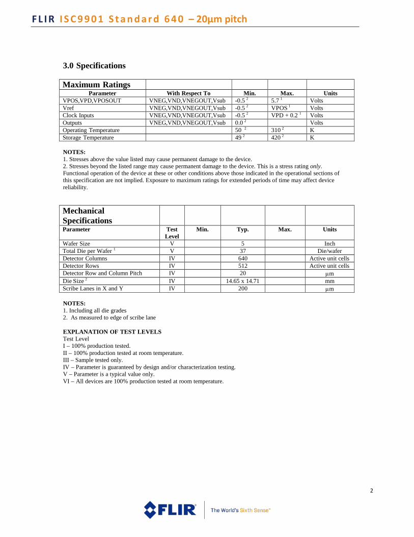
3.0 Specifications
Maximum Ratings Parameter With Respect To Min. Max. Units
VPOS,VPD,VPOSOUT VNEG,VND,VNEGOUT,Vsub -0.5 2 5.7 1 Volts Vref VNEG,VND,VNEGOUT,Vsub -0.5 2 VPOS 1 Volts Clock Inputs VNEG,VND,VNEGOUT,Vsub -0.5 2 VPD + 0.2 1
Volts Outputs VNEG,VND,VNEGOUT,Vsub 0.0 2 Volts Operating Temperature 50 2
310 2 K Storage Temperature 49 2 420 2 K
NOTES: 1. Stresses above the value listed may cause permanent damage to the device. 2. Stresses beyond the listed range may cause permanent damage to the device. This is a stress rating only. Functional operation of the device at these or other conditions above those indicated in the operational sections of this specification are not implied. Exposure to maximum ratings for extended periods of time may affect device reliability.
Mechanical Specifications
Parameter Test Level
Min. Typ. Max. Units
Wafer Size V 5 Inch Total Die per Wafer 1
V 37 Die/wafer Detector Columns IV 640 Active unit cells Detector Rows IV 512 Active unit cells Detector Row and Column Pitch IV 20 µm Die Size 2 IV 14.65 x 14.71 mm Scribe Lanes in X and Y IV 200 µm
NOTES: 1. Including all die grades 2. As measured to edge of scribe lane
EXPLANATION OF TEST LEVELS Test Level I – 100% production tested. II – 100% production tested at room temperature. III – Sample tested only. IV – Parameter is guaranteed by design and/or characterization testing. V – Parameter is a typical value only. VI – All devices are 100% production tested at room temperature.

F L I R I S C 9 9 0 1 S t a n d a r d 6 4 0 – 20µm pitch
3
DC Specifications (50-300K operation unless noted)
Parameter Test
Level Min. Typ. Max. Units
Output Rate, Single output mode (80 or 300K) 6 II 12.3 Mpixels Output Rate, 2 or 4 output mode (80 or 300K) 6 IV 10 MPixels Max 640 x 480 Window Frame Rate @80K 4 Output Mode (Tint=1ms, max power) Note 13 95 Frames/sec 2 Output Mode (Tint=1ms, max power) Note 13 55 Frames/sec 1 Output Mode (Tint=1ms, max power) Note 13 30 Frames/sec Max Frame Rate @ 80K, min. window size 4 Output Mode, max power 128 x 8 IV 930 Frames/sec 2 Output Mode, max power 64 x 8 IV 930 Frames/sec 1 Output Mode, max power 32 x 8 IV 930 Frames/sec Output Voltage Swing 6
VI 2.1 2.6 2.9 Volts Output Voltage Low 6
V 1.4 1.6 1.8 Volts Output Voltage High 6
V 3.9 4.1 4.3 Volts Input Clock Rate IV DC 3 6.15 15
MHz Output Noise 8 Gain 00 IV 123 µV Gain 01 IV 145 µV Gain 10 IV 182 µV Gain 11 IV 302 µV Equiv. Integration Capacitor Input Noise 8
Gain 00 IV 321 e-
Gain 01 IV 284 e-
Gain 10 IV 238 e-
Gain 11 IV 197 e-
Gain Gain 00 (Relative Gain 1.0) IV 0.46 µV/e-
Gain 01 (Relative Gain 1.33) IV 0.61 µV/e-
Gain 10 (Relative Gain 2.0) IV 0.91 µV/e-
Gain 11 (Relative Gain 4.0) IV 1.83 µV/e-
Transimpedance Non-Linearity 10 IV ±0.1% <0.5%
Unit Cell Input Detector Capacitance 7
IV ≤ 0.5 pf Detector Impedance 7 IV > 1e+03 Ohms*cm2
Full Well Capacity 350fF Cint (150fF)11, @3.2V IV 6.3e6
(2.7e6) 7e6
(3e6) 7.7e6
(3.3e6) e-
Input Current 7 IV .001 1.0 10 nA NOTES: 1. Category IV for specified min., category VI for specified max.
2. Category IV for specified min. and max., category VI for specified typ. 3. Voltages below Vnd may cause excess power dissipation. 4. Voltages above Vpd may cause excess power dissipation. 5. Typical value tested 6. ≤0.25pf max., >100K ohms min. 7. Simulation range. 8. Zero detector current. 9. Imstr_adj set for 100 uA 10. As measured by output voltage vs Tint; Max deviation from a least squares fit over 10% to 80% full well. 11. ISC9901-2 Version 12. Relative gain measured. 13. Category IV for 80K, category VI 300K. 14. For high reverse bias configurations (e.g. QWIP) 15. Output pixel rate is twice the input clock rate

F L I R I S C 9 9 0 1 S t a n d a r d 6 4 0 – 20µm pitch
4
DC Specifications (cont) Test
Level Min. Typical Max. Units
Operability Percentage 99.998 % Bad Pixel Cluster Size 50 pixels On Chip Detector Bias DAC Input Voltage Range (forward to reverse bias) VI -195 to 425
(300K) -120 to 520 (80K)
mV
DAC Bits V 7 Voltage Resolution VI 5 mV/count Temperature Sensor Output @ 300K V 0.65 0.70 0.75 Volts Temperture Sensor Output @ 78K IV 1.02 1.070 1.12 Volts Power Supply Voltages (wrt VNEG,VND,VNEGOUT,Vsub)
VDETCOM Note 1 0 5.5 6.0 14
Volts VPOS Note 1 5.3 5.5 5.7 Volts VPOSOUT Note 1 5.3 5.5 5.7 Volts VPD Note 1 5.3 5.5 5.7 Volts Reference and Control Voltage Inputs VREF Note 2 1.5 1.6 1.7 Volts VOUTREF Note 2 1.5 1.6 1.7 Volts VDET_ADJ 0 5.5 Volts IMSTR_ADJ IV 0 3 5.5 Volts VOS IV VREF VPOS Volts Power Suppy Currents VDETCOM V <1 <10 (peak) mA VPOS V <17 <60 (peak) mA VPOSOUT V <25 <80 (peak) mA VPD V <4 <60 (peak) mA Logic Inputs Input Low Voltage II VND - 0.2 3
VND VND + 0.2 Volts Input High Voltage II VPD - 0.2 VPD VPD + 0.2 4
Volts Power Consumption 9 Single Output NTSC/PAL IV 90 mW Four Output Max Frame Rate IV 180 mW Integration Time 640 x 480
1 Output @ 12.3MHz, Interlaced
4 Outputs @ 10MHz, Non-Interlaced
IV 0.1 User adjustable
≥ 6.5 msec @ 30Hz Frame Rate
≥ 7.35 msec @ 60Hz Frame Rate
msec
F L I R I S C 9 9 0 1 S t a n d a r d 6 4 0 – 20µm pitch
5
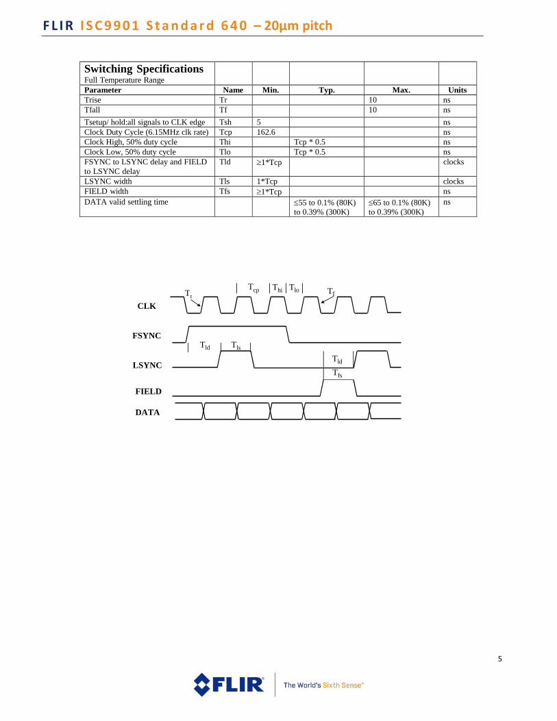
Switching Specifications Full Temperature Range
Parameter Name Min. Typ. Max. Units Trise Tr 10 ns Tfall Tf 10 ns Tsetup/ hold:all signals to CLK edge Tsh 5 ns Clock Duty Cycle (6.15MHz clk rate) Tcp 162.6 ns Clock High, 50% duty cycle Thi Tcp * 0.5 ns Clock Low, 50% duty cycle Tlo Tcp * 0.5 ns FSYNC to LSYNC delay and FIELD to LSYNC delay
Tld ≥1*Tcp clocks
LSYNC width Tls 1*Tcp clocks FIELD width Tfs ≥1*Tcp ns DATA valid settling time ≤55 to 0.1% (80K)
to 0.39% (300K) ≤65 to 0.1% (80K) to 0.39% (300K)
ns
CLK
FSYNC
LSYNC
FIELD
DATA
T Tcp Thi Tlo
r Tf
Tld Tls
Tld
Tfs
F L I R I S C 9 9 0 1 S t a n d a r d 6 4 0 – 20µm pitch
6
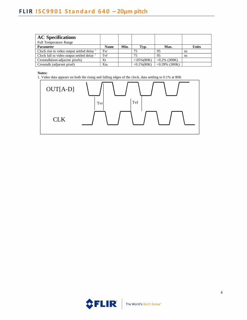
AC Specifications Full Temperature Range
Parameter Name Min. Typ. Max. Units Clock rise to video output settled delay 1
Tvr 75 95 ns Clock fall to video output settled delay 1
Tvf 75 95 ns Crosstalk(non-adjacent pixels) Xt <.05%(80K) <0.2% (300K) Crosstalk (adjacent pixel) Xta <0.1%(80K) <0.39% (300K)
Notes: 1. Video data appears on both the rising and falling edges of the clock, data settling to 0.1% at 80K
OUT[A-D]
Tvr Tvf
CLK
F L I R I S C 9 9 0 1 S t a n d a r d 6 4 0 – 20µm pitch
7
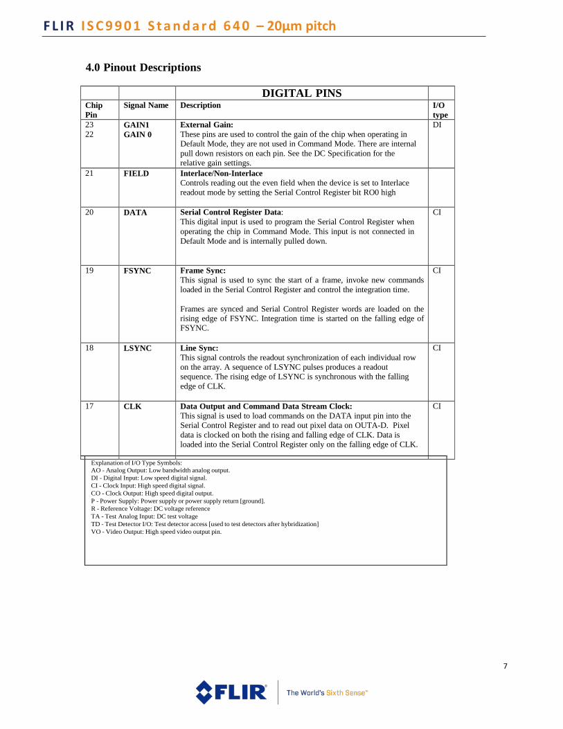
4.0 Pinout Descriptions DIGITAL PINS
Chip Pin
Signal Name Description I/O type
23 22
GAIN1 GAIN 0
External Gain: These pins are used to control the gain of the chip when operating in Default Mode, they are not used in Command Mode. There are internal pull down resistors on each pin. See the DC Specification for the relative gain settings.
DI
21 FIELD Interlace/Non-Interlace Controls reading out the even field when the device is set to Interlace readout mode by setting the Serial Control Register bit RO0 high
20 DATA Serial Control Register Data: This digital input is used to program the Serial Control Register when operating the chip in Command Mode. This input is not connected in Default Mode and is internally pulled down.
CI
19 FSYNC Frame Sync: This signal is used to sync the start of a frame, invoke new commands loaded in the Serial Control Register and control the integration time.
Frames are synced and Serial Control Register words are loaded on the rising edge of FSYNC. Integration time is started on the falling edge of FSYNC.
CI
18 LSYNC Line Sync: This signal controls the readout synchronization of each individual row on the array. A sequence of LSYNC pulses produces a readout sequence. The rising edge of LSYNC is synchronous with the falling edge of CLK.
CI
17 CLK Data Output and Command Data Stream Clock: This signal is used to load commands on the DATA input pin into the Serial Control Register and to read out pixel data on OUTA-D. Pixel data is clocked on both the rising and falling edge of CLK. Data is loaded into the Serial Control Register only on the falling edge of CLK.
CI
Explanation of I/O Type Symbols: AO - Analog Output: Low bandwidth analog output. DI - Digital Input: Low speed digital signal. CI - Clock Input: High speed digital signal. CO - Clock Output: High speed digital output. P - Power Supply: Power supply or power supply return [ground]. R - Reference Voltage: DC voltage reference TA - Test Analog Input: DC test voltage TD - Test Detector I/O: Test detector access [used to test detectors after hybridization] VO - Video Output: High speed video output pin.
FLIR ISC9901 Standard 640/20
8
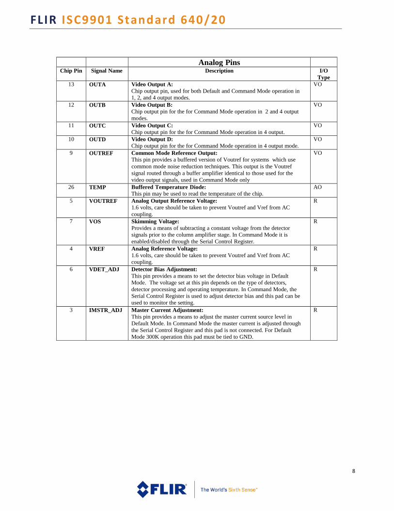
Analog Pins
Chip Pin Signal Name Description I/O Type
13 OUTA Video Output A: Chip output pin, used for both Default and Command Mode operation in 1, 2, and 4 output modes.
VO
12 OUTB Video Output B: Chip output pin for the for Command Mode operation in 2 and 4 output modes.
VO
11 OUTC Video Output C: Chip output pin for the for Command Mode operation in 4 output.
VO
10 OUTD Video Output D: Chip output pin for the for Command Mode operation in 4 output mode.
VO
9 OUTREF Common Mode Reference Output: This pin provides a buffered version of Voutref for systems which use common mode noise reduction techniques. This output is the Voutref signal routed through a buffer amplifier identical to those used for the video output signals, used in Command Mode only
VO
26 TEMP Buffered Temperature Diode: This pin may be used to read the temperature of the chip.
AO
5 VOUTREF Analog Output Reference Voltage: 1.6 volts, care should be taken to prevent Voutref and Vref from AC coupling.
R
7 VOS Skimming Voltage: Provides a means of subtracting a constant voltage from the detector signals prior to the column amplifier stage. In Command Mode it is enabled/disabled through the Serial Control Register.
R
4 VREF Analog Reference Voltage: 1.6 volts, care should be taken to prevent Voutref and Vref from AC coupling.
R
6 VDET_ADJ Detector Bias Adjustment: This pin provides a means to set the detector bias voltage in Default Mode. The voltage set at this pin depends on the type of detectors, detector processing and operating temperature. In Command Mode, the Serial Control Register is used to adjust detector bias and this pad can be used to monitor the setting.
R
3 IMSTR_ADJ Master Current Adjustment: This pin provides a means to adjust the master current source level in Default Mode. In Command Mode the master current is adjusted through the Serial Control Register and this pad is not connected. For Default Mode 300K operation this pad must be tied to GND.
R
F L I R I S C 9 9 0 1 S t a n d a r d 6 4 0 – 20µm pitch
9
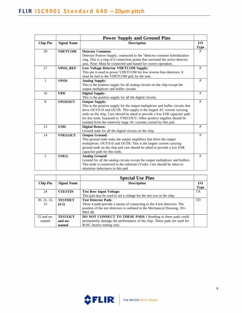
Power Supply and Ground Pins
Chip Pin Signal Name Description I/O Type
28 VDETCOM Detector Common: Detector Postive Supply, connected to the “detector common hybridization ring. This is a ring of 6 connection points that surround the active detector area. Note: Must be connected and biased for correct operation.
P
27 VPOS_REF Low Voltage Detector VDETCOM Supply: This pin is used to power VDETCOM for low reverse bias detectors. It must be tied to the VDETCOM pad, by the user.
P
1 VPOS Analog Supply: This is the positive supply for all analog circuits on the chip except the output multiplexer and buffer circuits.
P
16 VPD Digital Supply: This is the positive supply for all the digital circuits.
P
8 VPOSOUT Output Supply: This is the positive supply for the output multiplexer and buffer circuits that drive OUTA-D and OUTR. This supply is the largest AC current carrying node on the chip. Care should be taked to provide a low ESR capacitor path for this node, bypassed to VNEGOUT. Other positive supplies should be isolated from the relatively large AC currents carried by this pad.
P
15 VND Digital Return: Ground node for all the digital circuits on the chip.
P
14 VNEGOUT Output Ground: This ground node sinks the output amplifiers that drive the output multiplexer, OUTA-D and OUTR. This is the largest current carrying ground node on the chip and care should be taked to provide a low ESR capacitor path for this node.
P
2 VNEG Analog Ground: Ground for all the analog circuits except the output multiplexer and buffers. This node is connected to the substrate (Vsub). Care should be taken to minimize inductance to this pad.
P
Special Use Pins
Chip Pin Signal Name Description I/O Type
24 VTESTIN Test Row Input Voltage: This pad may be used to set a voltage for the test row in the chip.
TA
30, 31, 32, 33
TESTDET (4-1)
Test Detector Pads: These 4 pads provide a means of connecting to the 4 test detectors. The position of the test detectors is outlined in the Mechanical Drawing, 101- 9901-80.
TD
25 and un- named
TESTOUT and un- named
DO NOT CONNECT TO THESE PADS ! Bonding to these pads could permanently damage the performance of the chip. These pads are used for ROIC factory testing only.
F L I R I S C 9 9 0 1 S t a n d a r d 6 4 0 – 20µm pitch
10
5.0 Theory of Operation A general description of the ISC9901 operation is given in this section.
Input Circuit
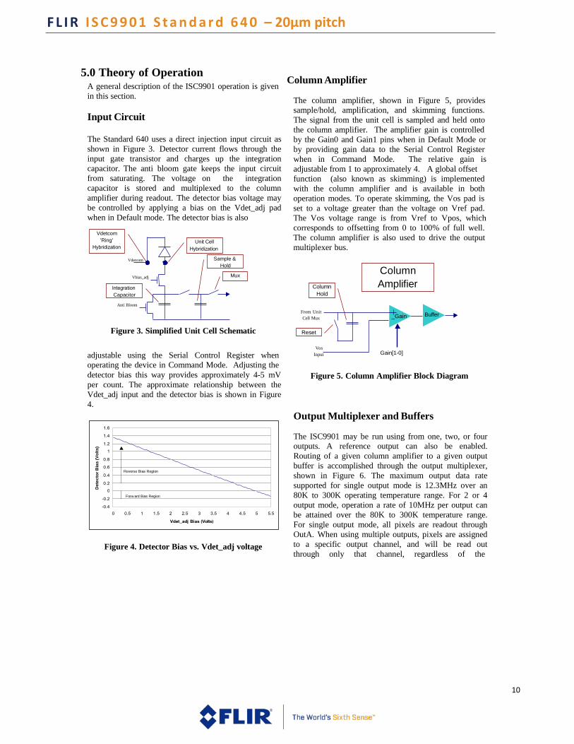
The Standard 640 uses a direct injection input circuit as shown in Figure 3. Detector current flows through the input gate transistor and charges up the integration capacitor. The anti bloom gate keeps the input circuit from saturating. The voltage on the integration capacitor is stored and multiplexed to the column amplifier during readout. The detector bias voltage may be controlled by applying a bias on the Vdet_adj pad when in Default mode. The detector bias is also
Column Amplifier
The column amplifier, shown in Figure 5, provides sample/hold, amplification, and skimming functions. The signal from the unit cell is sampled and held onto the column amplifier. The amplifier gain is controlled by the Gain0 and Gain1 pins when in Default Mode or by providing gain data to the Serial Control Register when in Command Mode. The relative gain is adjustable from 1 to approximately 4. A global offset function (also known as skimming) is implemented with the column amplifier and is available in both operation modes. To operate skimming, the Vos pad is set to a voltage greater than the voltage on Vref pad. The Vos voltage range is from Vref to Vpos, which corresponds to offsetting from 0 to 100% of full well. The column amplifier is also used to drive the output multiplexer bus.
Figure 3. Simplified Unit Cell Schematic
adjustable using the Serial Control Register when operating the device in Command Mode. Adjusting the
From Unit Cell Mux
Vos Input
Gain
Gain[1-0]
Buffer
detector bias this way provides approximately 4-5 mV per count. The approximate relationship between the Vdet_adj input and the detector bias is shown in Figure 4.
Reverse Bias Region
Forw ard Bias Region
Figure 4. Detector Bias vs. Vdet_adj voltage
Figure 5. Column Amplifier Block Diagram
Output Multiplexer and Buffers
The ISC9901 may be run using from one, two, or four outputs. A reference output can also be enabled. Routing of a given column amplifier to a given output buffer is accomplished through the output multiplexer, shown in Figure 6. The maximum output data rate supported for single output mode is 12.3MHz over an 80K to 300K operating temperature range. For 2 or 4 output mode, operation a rate of 10MHz per output can be attained over the 80K to 300K temperature range. For single output mode, all pixels are readout through OutA. When using multiple outputs, pixels are assigned to a specific output channel, and will be read out through only that channel, regardless of the
Column Hold
Column Amplifier
Reset
Vdetcom'Ring'
Capacitor
Unit Cell
Sample &Hold
Vdetcom
Vbias_adj Mux
Anti Bloom
Det
ecto
r Bia
s (V
olts
)
FLIR ISC9901 Standard 640/20
11
invert/revert, windowing, and/or line repeat modes selected.
From Column
Amp Buffers
Figure 6. Output Multiplexer and Buffers
Integration
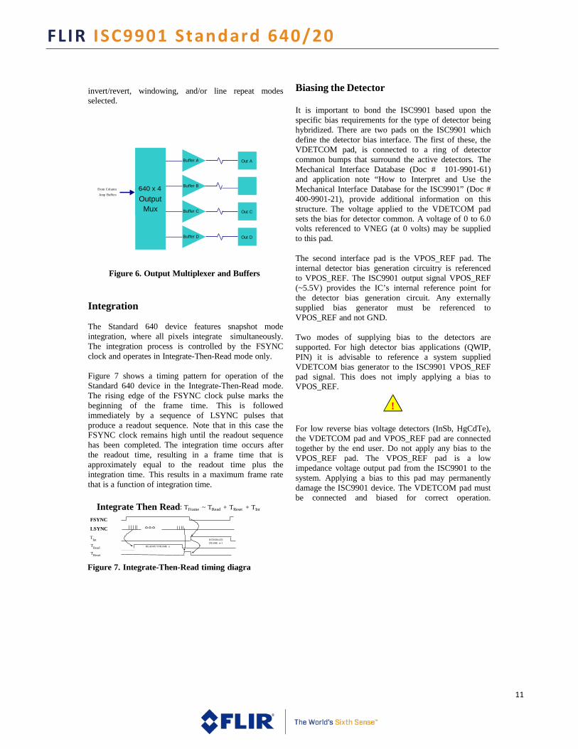
The Standard 640 device features snapshot mode integration, where all pixels integrate simultaneously. The integration process is controlled by the FSYNC clock and operates in Integrate-Then-Read mode only.
Figure 7 shows a timing pattern for operation of the Standard 640 device in the Integrate-Then-Read mode. The rising edge of the FSYNC clock pulse marks the beginning of the frame time. This is followed immediately by a sequence of LSYNC pulses that produce a readout sequence. Note that in this case the FSYNC clock remains high until the readout sequence has been completed. The integration time occurs after the readout time, resulting in a frame time that is approximately equal to the readout time plus the integration time. This results in a maximum frame rate that is a function of integration time.
Integrate Then Read: TFrame ~ TRead + TReset + TInt
FSYNC
LSYNC TInt
TRead
TReset
Biasing the Detector
It is important to bond the ISC9901 based upon the specific bias requirements for the type of detector being hybridized. There are two pads on the ISC9901 which define the detector bias interface. The first of these, the VDETCOM pad, is connected to a ring of detector common bumps that surround the active detectors. The Mechanical Interface Database (Doc # 101-9901-61) and application note “How to Interpret and Use the Mechanical Interface Database for the ISC9901” (Doc # 400-9901-21), provide additional information on this structure. The voltage applied to the VDETCOM pad sets the bias for detector common. A voltage of 0 to 6.0 volts referenced to VNEG (at 0 volts) may be supplied to this pad.
The second interface pad is the VPOS_REF pad. The internal detector bias generation circuitry is referenced to VPOS_REF. The ISC9901 output signal VPOS_REF (~5.5V) provides the IC’s internal reference point for the detector bias generation circuit. Any externally supplied bias generator must be referenced to VPOS_REF and not GND.
Two modes of supplying bias to the detectors are supported. For high detector bias applications (QWIP, PIN) it is advisable to reference a system supplied VDETCOM bias generator to the ISC9901 VPOS_REF pad signal. This does not imply applying a bias to VPOS_REF.
For low reverse bias voltage detectors (InSb, HgCdTe), the VDETCOM pad and VPOS_REF pad are connected together by the end user. Do not apply any bias to the VPOS_REF pad. The VPOS_REF pad is a low impedance voltage output pad from the ISC9901 to the system. Applying a bias to this pad may permanently damage the ISC9901 device. The VDETCOM pad must be connected and biased for correct operation.
Figure 7. Integrate-Then-Read timing diagra
!
Buffer A Out A
Buffer B Out B
Buffer C Out C
Buffer D Out D
640 x 4 Output
Mux
FLIR ISC9901 Standard 640/20
12
15 16 17 18 19 20 21 22 23 24 25 26 27 28 29
30
31
32
33
14 13 12 11 10 9 8 7 6 5 4 3 2 1
VN
EG
IMSTR
_AD
J
6.1 Modes of Operation The ISC9901 has two operation modes, the simplified Default Mode and the programmable Command Mode which utilizes the advanced features of the ROIC.
Default Mode
This mode provides a simple interface, with reduced external electronics and power dissipation, for applications where advanced ROIC features or high- speed performance are not required. The Default Mode does not use the on chip Serial Control Register. Therefore, advanced features such as windowing, invert/revert and multiple data outputs are not available. The Default Mode supports operation with both high and low reverse bias detectors by using a special biasing procedure. In Default Mode the ISC9901 operates with the following configuration:
• single output • variable gain • full window • normal scan order, interlaced readout • no reference output • supporting NTSC or PAL video timing • maximum output rate 12.3MHz • skimming
R
OW
REGISTER
INPUT CELL ARRAY (640 X 512)
COLUMN AMPS, COLUMN REGISTER
A total of 19 interconnects are required for Default Mode as shown in Figure 8.
Figure 8. Default Mode Bond Pad Diagram
Command Mode
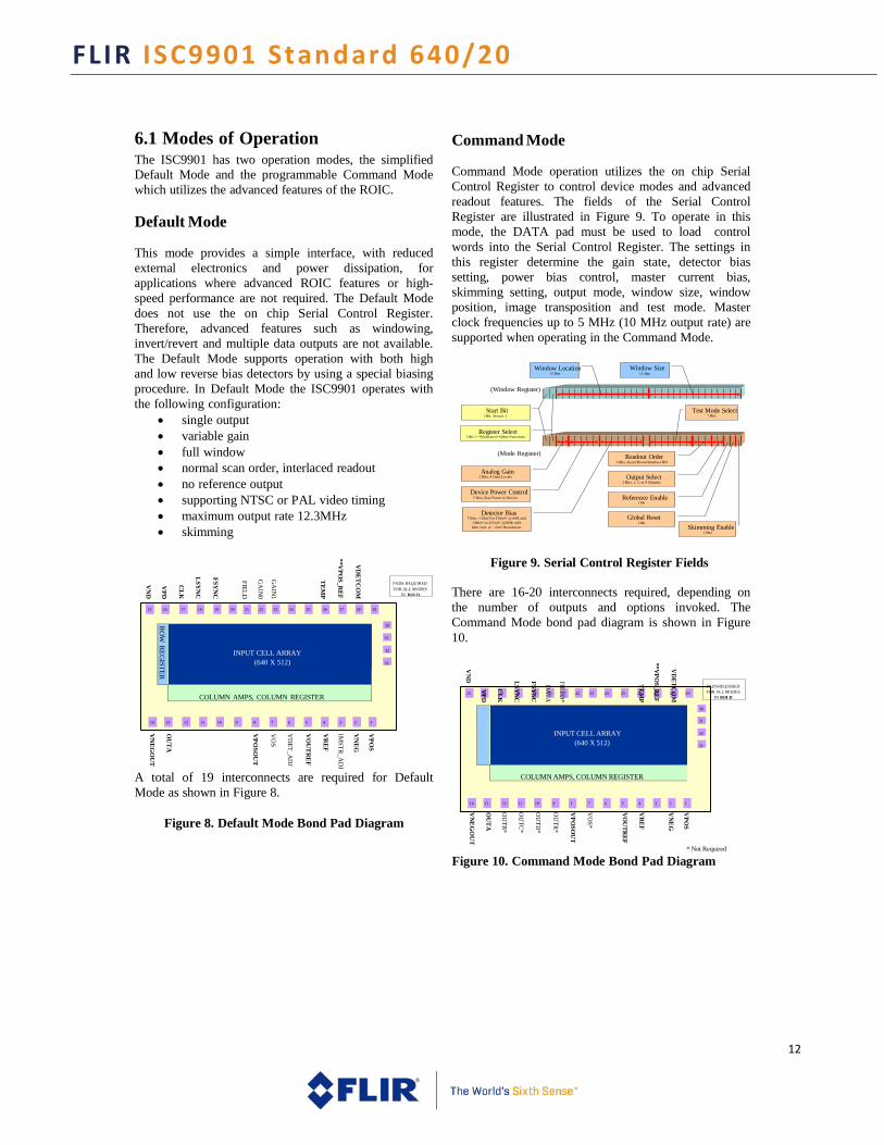
Command Mode operation utilizes the on chip Serial Control Register to control device modes and advanced readout features. The fields of the Serial Control Register are illustrated in Figure 9. To operate in this mode, the DATA pad must be used to load control words into the Serial Control Register. The settings in this register determine the gain state, detector bias setting, power bias control, master current bias, skimming setting, output mode, window size, window position, image transposition and test mode. Master clock frequencies up to 5 MHz (10 MHz output rate) are supported when operating in the Command Mode.
Figure 9. Serial Control Register Fields
There are 16-20 interconnects required, depending on the number of outputs and options invoked. The Command Mode bond pad diagram is shown in Figure 10.
* Not Required
Figure 10. Command Mode Bond Pad Diagram
PADS REQUIRED FOR ALL MODES
IN BOLD
Window Size
Test Mode Select
Register Select
Analog Gain
Device Power Control
Detector Bias
Readout Order
Output Select
Reference Enable
Global Reset
Skimming Enable
Window Location
(Window Register) Start Bit
(Mode Register)
15 16 17 18 19 20 21 22 23 24 25 26 27 28 29
30 31
32
33
14 13 12 11 10 9 8 4 3 2 1
PADS REQUIRED FOR ALL MODES
IN BOLD
VPO
S
VD
ETCO
M
VN
EG
**VPOS_R
EF
TEMP
VR
EF
VO
UTR
EF
VO
S*
VPO
SOU
T
FIELD*
OU
TR*
DA
TA
OU
TD*
FSYN
C
OU
TC*
LSYN
C
OU
TB*
CLK
OU
TA
VPD RO
W R
EGISTER
V
NEG
OU
T
VN
D
VPO
S
VD
ETC
OM
**VPO
S_REF
VR
EF TEM
P
VO
UT
REF
VD
ET_AD
J
GA
IN1
GA
IN0
VO
S
VPO
SOU
T
FIELD
FSYN
C
LSYN
C
CLK
OU
TA
VPD
VN
EGO
UT
VN
D
INPUT CELL ARRAY (640 X 512)
COLUMN AMPS, COLUMN REGISTER
FLIR ISC9901 Standard 640/20
13
Output Modes
The ISC9901 can be configured to support one, two, four outputs with or without an output reference. In order to invoke any output mode other than single output, with no reference output, the device must be operated in Command Mode. For single output mode, all pixels are read out through OutA. When using multiple outputs, pixels are assigned to a specific output channel, and will be read out through only that channel, regardless of the image transposition (invert/revert), and windowing modes selected.
The lowest left-hand pixel is defined as pixel (0,0), where this annotation signifies the pixel at location row 0, column 0 of the ISC9901 device. Pixel (0,0) is the first pixel to be read out in using default settings for the invert/revert, windowing, and line repeat features. This mode of operation is chosen for a normal ‘inverting optic’. Given this type of optic, a ‘normal’ raster scan image will be presented by placing the bottom row (row 0) at the ‘bottom’ of a camera system.
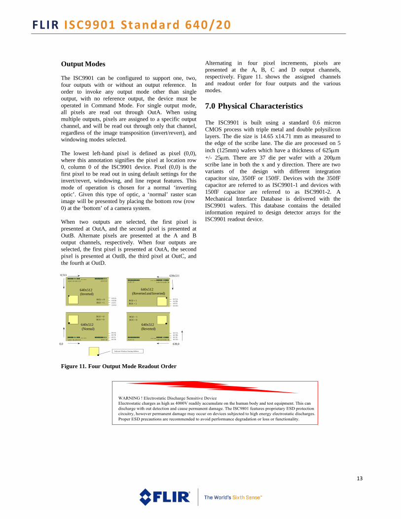
When two outputs are selected, the first pixel is presented at OutA, and the second pixel is presented at OutB. Alternate pixels are presented at the A and B output channels, respectively. When four outputs are selected, the first pixel is presented at OutA, the second pixel is presented at OutB, the third pixel at OutC, and the fourth at OutD.
Alternating in four pixel increments, pixels are presented at the A, B, C and D output channels, respectively. Figure 11. shows the assigned channels and readout order for four outputs and the various modes.
7.0 Physical Characteristics
The ISC9901 is built using a standard 0.6 micron CMOS process with triple metal and double polysilicon layers. The die size is 14.65 x14.71 mm as measured to the edge of the scribe lane. The die are processed on 5 inch (125mm) wafers which have a thickness of 625µm +/- 25µm. There are 37 die per wafer with a 200µm scribe lane in both the x and y direction. There are two variants of the design with different integration capacitor size, 350fF or 150fF. Devices with the 350fF capacitor are referred to as ISC9901-1 and devices with 150fF capacitor are referred to as ISC9901-2. A Mechanical Interface Database is delivered with the ISC9901 wafers. This database contains the detailed information required to design detector arrays for the ISC9901 readout device.
0,511 ….
A B C D A B C D
A B C D A B C D
639x511
…. A B C D A B C D
640x512 (Inverted)
RO2 = 0 RO1 = 1
OUTA OUTB OUTC OUTD
640x512
(Reverted and Inverted)
RO2 = 1 RO1 = 1
OUTA OUTB OUTC OUTD
0,0
640x512 (Normal)
….
A B C D A B C D
RO2 = 0 RO1 = 0
A B C D
OUTA OUTB OUTC OUTD
RO2 = 1 RO1 = 0
A B C D
640x512 (Reverted)
….
A B C D A B C D
OUTA OUTB OUTC OUTD
639,0
Figure 11. Four Output Mode Readout Order
Indicates Window Starting Address