equivalent circuits for mis microstrip discontinuities
TRANSCRIPT
408 IEEE MICROWAVE AND GUIDED WAVE LElTERS, VOL. 3, NO. 1 1 , NOVEMBER 1993
Equivalent Circuits for MIS Microstrip Discontinuities
Jes6s Martel, Rafael R. Boix, and Manuel Homo, Member, ZEEE
Abstruct- Metal-insulator-semiconductor (MIS) microstrip open-end and microstrip gap discontinuities are characterized by means of equivalent circuits consisting of capacitors and resistors. The circuit parameters of these components are obtained in terms of the complex excess charge densities existing on the conducting strips of the discontinuities. These complex excess charge densities are computed by applying Galerkin’s method in the spectral domain. The numerical results obtained for the equivalent circuit parameters of the discontinuities exhibit important variations with frequency, which become specially pronounced in the transition region between the slow-wave mode and the dielectric mode of the MIS microstrip lines involved in the discontinuities.
I. INTRODUCTION
ETAL-INSULATOR-SEMICONDUCTOR (MIS) mi- M crostrip lines have been proposed for being used in MMIC’s since their slow-wave properties make possible an important reduction in the size of circuit distributed compo- nents [l], [2]. Layered MIS microstrip lines have also been found to be appropriate for the modeling of interconnections in very-high-speed VLSI digital integrated circuits [ 11, [3], and for the modeling of Schottky contact microstrip lines with localized depletion regions [4]. Whereas guiding problems in MIS microstrip lines have been extensively treated [ 11, the existing information on the analysis of MIS microstrip discontinuities is comparatively scarce [ 5 ] . This letter provides original results on the equivalent circuit parameters of MIS microstrip open-end discontinuities and MIS microstrip gap discontinuities. The circuit parameters of the discontinuities are obtained by adapting the excess-charge technique in the spectral domain developed in [6] to the analysis of microstrip discontinuities embedded in a multilayered substrate consisting of both lossless and lossy materials. Since the methods of analysis employed in this letter are inherently static, they are expected to be correct for MIS microstrip discontinuities whose dimensions are much smaller than the lines wavelength and the substrate skin depth, and for semiconductor substrates having moderate conductivity values [7]. The fulfillment of these requirements has been checked on all the structures analyzed in the letter.
Manuscript received June 21, 1993. This work was wpported by the DGICYT, Spain (Project No. TIC91-1018).
The authors are with the Grup? de Microondas, Dpto. Electronica y Electromagnetismo, Facultad de Fisica, Avd. Reina Mercedes s/n, 4 I O 12 Seville, Spain.
IEEE Log Number 9212838.
11. DETERMINATION OF THE EQUIVALENT CIRCUITS OF THE DISCONTINUITIES
The equivalent circuits assigned to the MIS microstrip discontinuities analyzed in the current letter consist of ca- pacitors and resistors. In order to determine the capacitances and conductances of these capacitors and resistors, use has been made of the excess-charge technique in the spectral domain (ECTSD) [6]. When applying the ECTSD, lossy semiconductors have been treated as dielectric materials with a complex permittivity (t = r (1 - j a / 2 ~ f t ) , where t is the actual permittivity, f is the frequency and a is the conductivity). This has caused that some relevant quantities related to the application of the ECTSD-such as the Green’s function and the excess charge densities on the conduct- ing strips-have turned out to be complex and frequency- dependent. The capacitances and conductances related with the equivalent circuits of the discontinuities have been obtained in terms of the real and imaginary parts of the complex excess-charge densities on the conducting strips respectively. As an example of how this is accomplished, let a,,(r) be the complex excess charge density on the conducting strip of a MIS microstrip open-end (see Fig. l), let S be the surface of the strip, let V be the potential on the strip, and let f be the frequency. The capacitance C, and the conductance G, appearing in the equivalent circuit of the MIS microstrip open-end (see Fig. 1) can be obtained in terms of aex(r), V and f as
C, = Re [ $ sex( r) ‘i.]
where Re and Im stand for real and imaginary parts respec- tively.
In order to solve the integral equations satisfied by the excess charge densities on the conducting strips of the discon- tinuities, Galerkin’s method in the spectral domain has been applied. The basis functions used in the approximation of the excess charge densities have been taken from [6].
It has been found that there are numerical differences between applying the ECTSD to the analysis of MIS microstrip discontinuities and applying the ECTSD to the analysis of conventional microstrip discontinuities. One of the differences is that the CPU time required to calculate the integrals ap- pearing in the spectral analysis [6] is higher in the case of MIS microstrip discontinuities than in the case of conventional microstrip discontinuities, the reason being that the integrands
IEEE MICROWAVE AND GUIDED WAVE LE'ITERS. VOL 3. NO. I I . NOVEMBER 1991
~
409
are worse behaved in the former case than in the latter case. Another difference is that the number of basis functions required to obtain accurate results (see Table I in [6]) in the case of MIS microstrip discontinuities doubles that required for conventional microstrip discontinuities. These two numerical differences are caused by the presence of very thin insulator layers (= 1 pm thick) in MIS structures and they have also been detected when comparing the analysis of MIS and conventional microstrip transmission lines [ 81.
111. RESULTS
As a check on our method of analysis, our results were com- pared in [ 101 with those obtained in [9] for microstrip open-end discontinuities fabricated on low-loss GaAs. It should be pointed out that excellent agreement was found between our results for the phase of ,511 under low-loss conditions and the results obtained by means of Touchstone in the lossless case UOI .
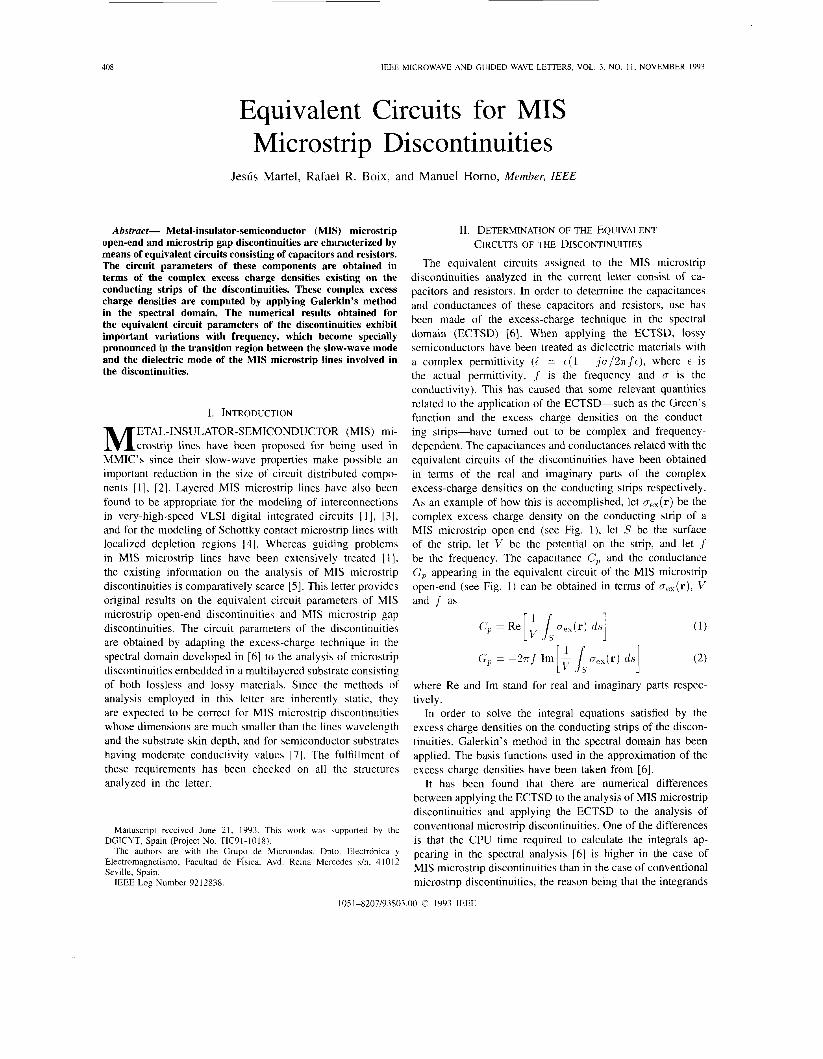
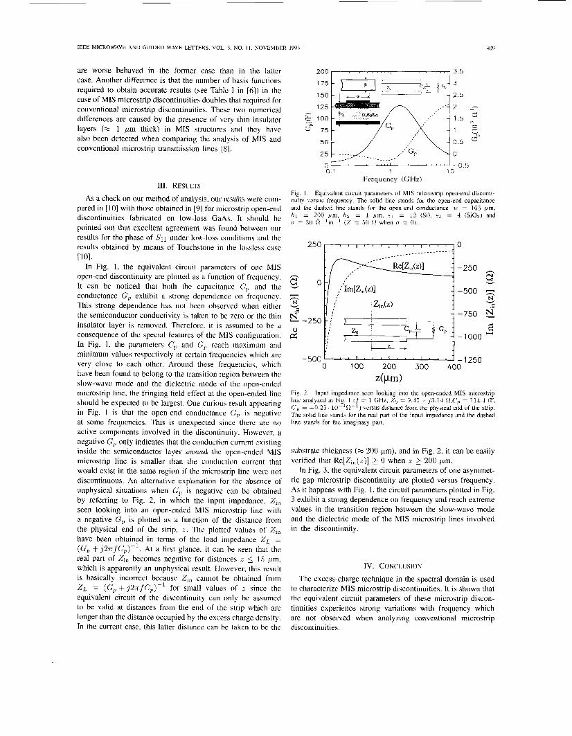
In Fig. 1, the equivalent circuit parameters of one MIS open-end discontinuity are plotted as a function of frequency. It can be noticed that both the capacitance C, and the conductance G, exhibit a strong dependence on frequency. This strong dependence has not been observed when either the semiconductor conductivity is taken to be zero or the thin insulator layer is removed. Therefore, i t is assumed to be a consequence of the special features of the MIS configuration. In Fig. 1, the parameters C, and G, reach maximum and minimum values respectively at certain frequencies which are very close to each other. Around these frequencies, which have been found to belong to the transition region between the slow-wave mode and the dielectric mode of the open-ended microstrip line, the fringing field effect at the open-ended line should be expected to be largest. One curious result appearing in Fig. 1 is that the open-end conductance G,, is negative at some frequencies. This is unexpected since there are no active components involved in the discontinuity. However, a negative G, only indicates that the conduction current existing inside the semiconductor layer around the open-ended MIS microstrip line is smaller than the conduction current that would exist in the same region if the microstrip line were not discontinuous. An alternative explanation for the absence of unphysical situations when G, is negative can be obtained by referring to Fig. 2, in which the input impedance, Z,, seen looking into an open-ended MIS microstrip line with a negative G, is plotted as a function of the distance from the physical end of the strip, z. The plotted values of Z,, have been obtained in terms of the load impedance Z L = (G, +j2r fCP) - ' . At a first glance, it can be seen that the real part of Zi, becomes negative for distances z 5 15 pm, which is apparently an unphysical result. However, this result is basically incorrect because Z,, cannot be obtained from ZL = (G, +j2rfC,)-' for small values of z since the equivalent circuit of the discontinuity can only be assumed to be valid at distances from the end of the strip which are longer than the distance occupied by the excess charge density. In the current case, this latter distance can be taken to be the
0 ' ' -0.5
,,*' G,
I 0 0.1 1 10
F r e q u e n c y (GHz)
Fig. 1 . Equivalent circuit parameters of MIS microstrip open-end disconti- nuity versus frequency. The solid line stands for the open-end capacitance and the dashed line stands for the open-end conductance. IL' = 165 pm, h , = 200 bm, h z = 1 p m , tl = 1 2 (Si), tz = 4 ( S O 2 ) and U = 30 Rp'mpl (Z = 50 (2 when 0 = 0 ) .
-250
-500
I . I & z d
z(pm)
-500 ' ' ' I " ' I " ' I " ' - 1250 100 200 300 400 0
Fig. 2. Input impedance seen looking into the open-ended MIS microstrip line analyzed in Fig. 1 (f = 1 GHz, Z" = 9.15 + j 3 . 1 4 n,C, = 114.4 fF, G, = -0.23. 10pJR-') versus distance from the physical end of the strip. The solid line stands for the real part of the input impedance and the dashed line stands for the imaginary part.
substrate thickness (= 200 pm), and in Fig. 2, it can be easily verified that Re[Zi,(z)] 2 0 when z 2 200 pm.
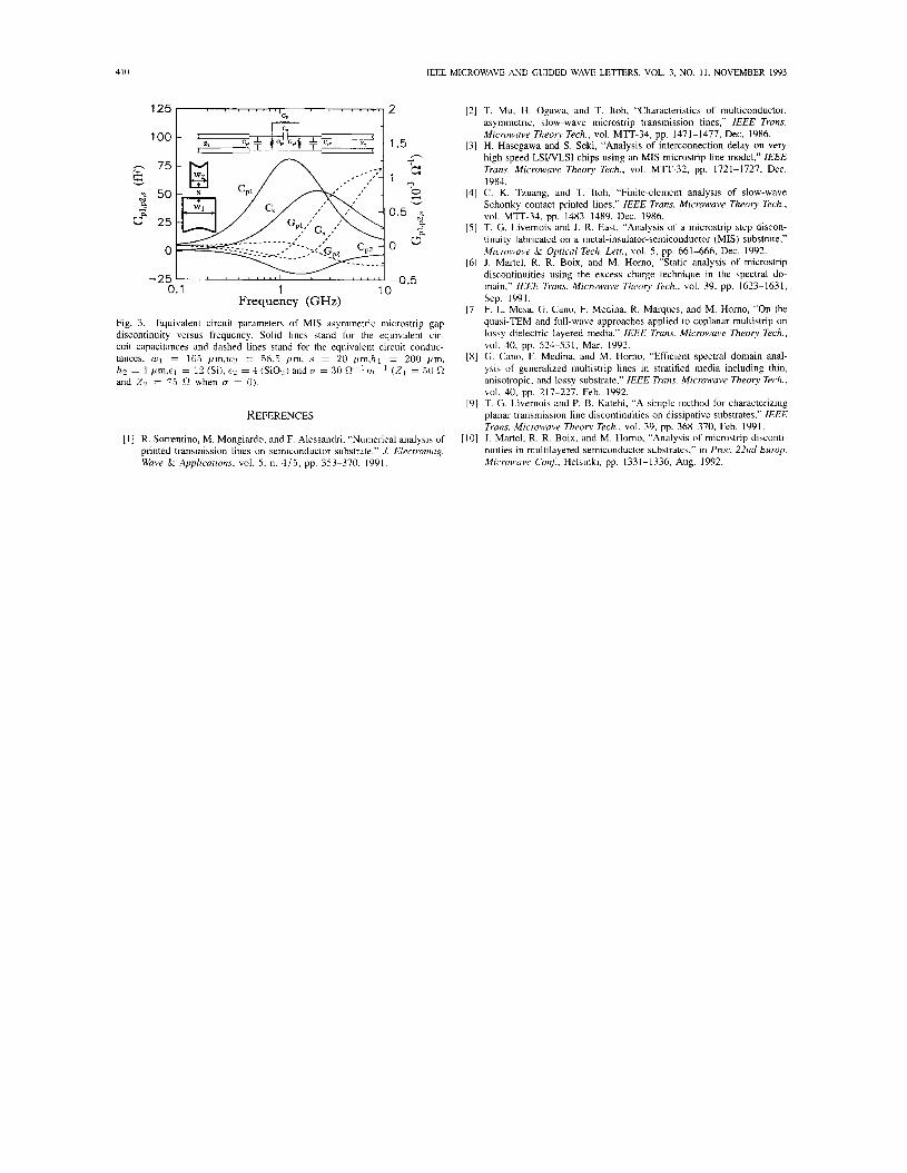
In Fig. 3, the equivalent circuit parameters of one asymmet- ric gap microstrip discontinuity are plotted versus frequency. As it happens with Fig. 1, the circuit parameters plotted in Fig. 3 exhibit a strong dependence on frequency and reach extreme values in the transition region between the slow-wave mode and the dielectric mode of the MIS microstrip lines involved in the discontinuity.
IV. CONCLUSION
The excess-charge technique in the spectral domain is used to characterize MIS microstrip discontinuities. It is shown that the equivalent circuit parameters of these microstrip discon- tinuities experience strong variations with frequency which are not observed when analyzing conventional microstrip discontinuities.
410
l o o -
IEEE MICROWAVE AND GUIDED WAVE LETTERS, VOL. 3, NO. 1 I . NOVEMBER 1993
-+ +v- 1.5 C.
h
. -
Frequency (GHz)
Fig. 3. Equivalent circuit parameters of MIS asymmetric microstrip gap discontinuity versus frequency. Solid lines stand for the equivalent cir- cuit capacitances and dashed lines stand for the equivalent circuit conduc- tances. w(~’1 = 165 pm,w2 = j8.5 jim, s = 2 0 jrm,h1 = 200 Itm, h2 = 1 pm,el = 1 2 (Si), € 2 = 4 (SiOz) and U = 30 Rp’rri-l (Z, = 50 R and 2 2 = 7.5 R when U = 0).
REFERENCES
[ l ] R. Sorrentino, M. Mongiardo, and F. Alessandri, “Numerical analysis of printed transmission lines on semiconductor substrate.” J. Elecrromag. Wave k Applications, vol. 5 , n. 415, pp. 353-370, 1991.
121 T. Mu, H. Ogawa, and T. Itoh, “Characteristics of multiconductor, asymmetric, slow-wave microstrip transmission lines,” IEEE Trans. Microwave Theory Tech., vol. M1T-34, pp. 1471-1477, Dec. 1986.
131 H. Hasegawa and S. Seki, “Analysis of interconnection delay on very high speed LSWLSI chips using an MIS microstrip line model,” IEEE Trans. Microwave Theory Tech., vol. MTT-32, pp. 1721-1727, Dec. 1984.
[4] C. K. Tzuang, and T. Itoh, “Finite-element analysis of slow-wave Schottky contact printed lines,’’ IEEE Trans. Microwave Theory Tech., vol. MTT-34, pp. 1483-1489, Dec. 1986.
151 T. G. Livemois and J. R. East, “Analysis of a microstrip step discon- tinuity fabricated on a metal-insulator-semiconductor (MIS) substrate,” Microwave k Opiical Tech. Lefi., vol. 5 , pp. 661-666, Dec. 1992.
161 J . Martel, R. R. Boix, and M. Homo, “Static analysis of microstrip discontinuities using the excess charge technique in the spectral do- main,” IEEE Trans. Microwave Theon Tech., vol. 39, pp. 1623-1631, Sep. 1991.
[7] F. L. Mesa, G. Cano, F. Medina, R. Marques, and M. Homo, “On the quasi-TEM and full-wave approaches applied to coplanar multistrip on lossy dielectric layered media,” IEEE Trans. Microwave Theory Tech., vol. 40, pp. 524-531, Mar. 1992.
[SI G. Cano, F. Medina, and M. Homo, “Efficient spectral domain anal- ysis of generalized multistrip lines in stratified media including thin, anisotropic, and lossy substrate,” IEEE Trans. Microwave Theory Tech., vol. 40, pp. 217-227, Feb. 1992.
191 T. G. Livemois and P. B. Katehi, “A simple method for characterizing planar transmission line discontinuities on dissipative substrates,’’ IEEE Trans. Microwave Theon Tech., vol. 39, pp. 368-370, Feb. 1991.
[IO] J . Martel, R. R. Boix, and M. Homo, “Analysis of microstrip disconti- nuities in multilayered semiconductor substrates,” in Proc. 22nd Europ. Microwave Conf , Helsinki, pp. 1331-1336, Aug. 1992.