active microstrip array antennas - edatop.com microstrip array antenna… · active microstrip...
TRANSCRIPT

ACTIVE MICROSTRIP ARRAY ANTENNAS
by
Chin Liong Yeo
The School of Computer Science and Electrical Engineering,
University of Queensland.
Submitted for the degree of Bachelor of Engineering (Honours)
in the division of Electrical and Electronic Engineering
October 2000

ii

iii
316 Sir Fred Schonell Drive
St Lucia, QLD 4067
Tel. (07) 37208582
October 20, 2000
The Dean
School of Engineering
University of Queensland
St Lucia, QLD 4072
Dear Professor Simmons,
In accordance with the requirements of the degree of Bachelor of Engineering
(Honours) in the division of Electrical and Electronic Engineering, I present the
following thesis entitled “Active Microstrip Array Antennas”. This work was performed
under the supervision of Associate Professor Marek E. Bialkowski.
I declare that the work submitted in this thesis is my own, except as
acknowledged in the text and footnotes, and has not been previously submitted for a
degree at the University of Queensland or any other institution.
Yours faithfully
Chin Liong Yeo

iv

v
To my family

vi
Acknowledgements
I wish to thank and acknowledge Associate Professor Marek E. Bialkowski for his time
and patience in guiding me during the course of this thesis. Without his invaluable
advises and assistance, the completion of this thesis would not be possible. In addition, I
would also like to express my appreciation and lots of thanks to Mr Hyok J. Song for
his assistance in answering many of my queries. Last but not least, special thanks to Mr
Damian G. Jones and Mr Richard R. Taylor for their assistance for the use of the
facilities at the microwave laboratory.

vii
Abstract
This thesis is concerned with investigations of two types of broadband antenna elements
that are to be used for spatial power combining. The first antenna is the Linearly
Tapered Slot Antenna (LTSA) while the second is the Uniplanar Quasi-Yagi antenna.
Both these antennas are to be fabricated with a high dielectric constant substrate
material (Duriod with dielectric constant εr = 10.2), substrate thickness of 0.635mm and
design frequency of 12.5GHz.
The first part of the thesis deals with the theory behind microstrip antennas and
transmission lines. An introduction to microstrip antennas is presented, followed by a
literature review on microstrip design equations and background information with
regard to microstrip broadband planar antennas. The three most commonly used
broadband planar antennas are illustrated, namely the Microstrip Patch antenna, Quasi-
Yagi antenna and Tapered Slot Antenna. In contrast to the microstrip patch, both the
LTSA and the Quasi-Yagi antenna radiates at the end-fire direction. As a result, both
these antennas can achieve higher gain, lower side lobes and wider bandwidth compared
to the conventional microstrip patch antenna. The second part of the thesis is concerned
with design procedures and considerations for both the antennas. The designs for the
two antennas are aimed at obtaining wider bandwidth and better radiation patterns. In
addition, a sensitivity analysis of the Quasi-Yagi antenna with respect to five design
parameters is demonstrated in chapter 6 of this thesis. The simulation of the Quasi-Yagi
is accomplished by using a commercially available full-wave (MoM) method of
moment analysis software package IE3D of Zeland Software Inc.
The simulation results showed that the Quasi-Yagi antenna is able to achieve a
simulated 36% frequency bandwidth for voltage standing-wave ratio VSWR < 2 at the
centre frequency of 12.5GHz. During the sensitivity analysis, it has been found that the
most sensitive parameters are the length of the driver, director and the distance from the
driver to the reflector. Variations to these three parameters will affect the antenna’s
performance in terms of return loss and operational frequency.

viii
Contents
Acknowledgement vi
Abstract vii
Contents viii
List of Figures xii
List of Tables xv
1 Introduction 1
1.1 Importance 1
1.2 Aim of Thesis 2
1.3 Outline of Thesis 2
2 Theory 5
2.1 Microstrip Transmission Line 6
2.1.1 Basic Microstrip Line 6
2.1.2 Microstrip Field Radiation 7
2.1.3 Substrate Materials 8
2.2 The Microstrip Antenna 11
2.2.1 Historical Development 11
2.2.2 Basic Microstrip Antenna 12
2.2.3 Radiated Fields of Microstrip Antenna 13

ix
2.2.4 Advantages vs. Disadvantages of Microstrip Antennas 14
2.2.5 Applications 16
2.3 Types of Microstrip Antennas 17
2.3.1 Microstrip Patch Antennas 17
2.3.2 Microstrip Travelling-Wave Antennas 18
2.3.3 Microstrip Slot Antennas 19
2.4 Excitation Techniques 20
2.4.1 Microstrip Feed 20
2.4.2 Coaxial Feed 22
3 Literature Review 23
3.1 Microstrip Design Formulas 24
3.1.1 Effective Dielectric Constant 24
3.1.2 Wavelength 25
3.1.3 Characteristic Impedance 26
3.1.4 Synthesis Equations 27
3.1.5 Microstrip Relationship Plots 29
3.2 Microstrip Discontinuities 30
4 Microstrip Broadband Planar Antennas 33
4.1 Microstrip Patch Antennas 34
4.1.1 Conventional Microstrip Patch Antenna 34
4.1.2 Aperture Coupled Microstrip Patch Antenna 35
4.1.3 Microstrip Patch Antenna Array 36
4.2 Microstrip Quasi-Yagi Antennas 38
4.2.1 Uniplanar Quasi-Yagi Antenna 38

x
4.2.2 Advantages and Disadvantages of Quasi-Yagi Antenna 40
4.3 Microstrip Tapered Slot Antennas 41
4.3.1 Types of Tapered Slot Antenna 41
4.3.2 Definition of E-plane and H-plane for TSAs 43
4.3.3 Advantages and Disadvantages of Tapered Slot Antenna 43
4.4 Spatial Power Combining 44
5 Design and Development of Microstrip Broadband Planar Antennas 47
5.1 Design of Uniplanar Quasi-Yagi Antenna 48
5.1.1 Design Considerations 48
5.1.2 Antenna Dimensions 49
5.2 Design of Linearly Tapered Slot Antenna 53
5.2.1 Design Considerations 53
5.2.2 Antenna Dimensions 54
6 Results and Discussion 57
6.1 Sensitivity Analysis of Quasi-Yagi Antenna 58
6.1.1 Length of Director 59
6.1.2 Distance Between Director and Driver 60
6.1.3 Distance Between Coupled Microstrip Lines 62
6.1.4 Length of Driver 64
6.1.5 Distance From the Driver to the Reflector 65
6.1.6 Final Design 67
6.2 Simulation Results of Quasi-Yagi Antenna 68
6.2.1 S11 Return Loss and Bandwidth 68
6.2.2 Voltage Standing-Wave Ratio 69

xi
6.2.3 Impedance Smith Chart and Average Current Density 70
6.2.4 Radiation Patterns of Quasi-Yagi Antenna 72
7 Summary and Future Prospects 75
7.1 Summary 75
7.2 Future Prospects 77
References 79

xii
List of Figures
2.1 Structure of microstrip transmission line 6
2.2 Electromagnetic field pattern of a microstrip 7
2.3 Basic configuration of microstrip antenna 12
2.4 Microstrip antenna and coordinate system 13
2.5 Various patch patterns used for microstrip patch antenna 17
2.6 Microstrip traveling-wave antennas 18
2.7 Microstrip slot antennas 19
2.8 Microstrip line fed antennas 21
2.9 Coaxial fed microstrip antennas 22
3.1 Extremely wide (w >> h) and extremely narrow (w << h) microstrip lines 24
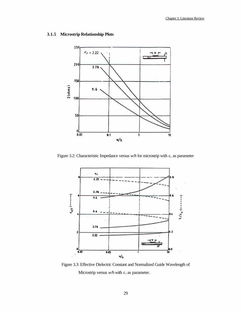
3.2 Characteristic impedance versus w/h for microstrip with ε r as parameter 29
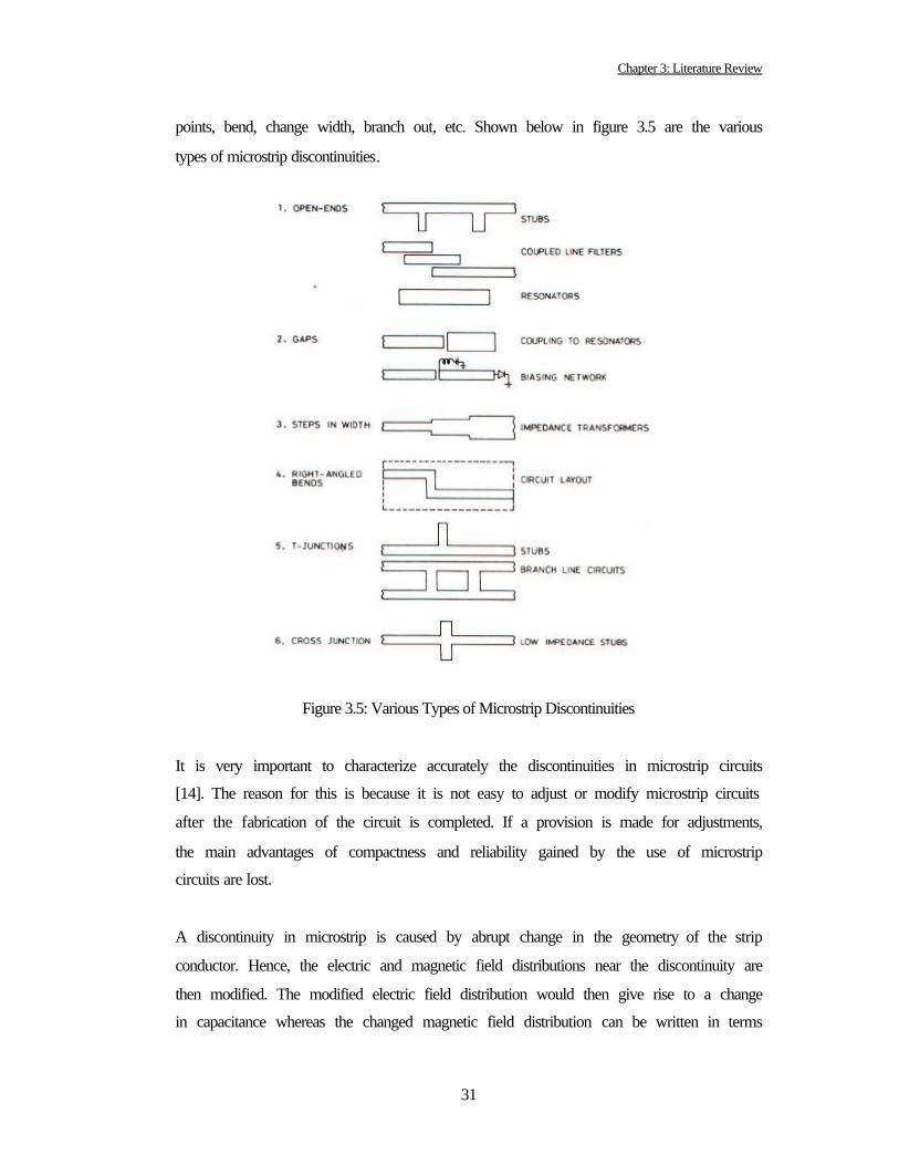
3.3 Effective dielectric constant and normalized guide wavelength of
microstrip versus w/h with ε r as parameter 29
3.4 Comparison of impedance characteristics of microstrip, suspended
microstrip and inverted microstrip. εr=3.78 30
3.5 Various types of microstrip discontinuities 31

xiii
4.1 Planar antenna selection chart 34
4.2 Broadside radiation direction of microstrip patch antenna 35
4.3 Microstrip aperture coupled patch antenna 36
4.4 Microstrip patch antenna array configurations 37
4.5 Uniplanar Quasi-Yagi antenna 39
4.6 End-fire radiation direction of Quasi-Yagi antenna 39
4.7 Different types of end-fire Tapered Slot Antenna 41
4.8 End-fire radiation pattern of Tapered Slot Antenna 42
4.9 Definition of E- and H- planes for TSAs 43
4.10 Four system configurations of circuit and spatial approaches 45
4.11 Spatially-Fed/Spatially-Combined approach 46
5.1 Schematic diagram of Quasi-Yagi Antenna 50
5.2 Actual size of Quasi-Yagi Antenna 53
5.3 Different sections of the LTSA 54
5.4 Top and bottom metalization of LTSA 55
6.1 Investigated parameters of the Quasi-Yagi antenna 58

xiv
6.2 Schematic diagram of Quasi-Yagi antenna from IE3D 67
6.3 S11 return loss of Quasi-Yagi Antenna 68
6.4 Simulated VSWR of the Quasi-Yagi Antenna 70
6.5 Impedance smith chart of Quasi-Yagi Antenna 70
6.6 Average current density at 12.5GHz 71
6.7 2D polar pattern of Quasi-Yagi Antenna 72
6.8 2D radiation pattern of Quasi-Yagi Antenna 72
6.9 3D radiation pattern of Quasi-Yagi Antenna 73
6.10 3D mapped pattern of Quasi-Yagi Antenna 73

xv
List of Tables
2.1 Properties of microwave dielectric substrates 10
2.2 Typical properties of RT/Duriod microwave materials 10

1
CHAPTER 1 INTRODUCTION This chapter highlights the importance of active array antennas to the present day
communication world. After defining the aim of this thesis, chapter one closes with an
overview of the thesis, listing a brief summary of the topics discussed in all of the
chapters of this thesis.
1.1 Importance
Communication can be broadly defined as the transfer of information from one point to
another. A communication system is usually required when the information is to be
conveyed over a distance. The transfer of information within the communication system
is commonly achieved by superimposing or modulating the information onto an
electromagnetic wave which acts as a carrier for the information signal. At the required
destination, the modulated carrier is then received and the original information signal

Chapter 1: Introduction
2
can be recovered by demodulation. Over the years, sophisticated techniques have been
developed for this process using electromagnetic carrier waves operating at radio
frequencies as well as microwave and millimeter wave frequencies.
In today’s modern communication industry, antennas are the most important
components required to create a communication link. Through the years, microstrip
antenna structures are the most common option used to realize millimeter wave
monolithic integrated circuits for microwave, radar and communication purposes. Due
to its many advantages over the conventional antenna, the microstrip antenna have
achieved importance and generated interest to antenna designers for many years. In fact,
active microstrip antenna arrays and active apertures are increasingly present in phased-
array radar applications. In addition, these devices also serve as potentially efficient
power combiners. Hence, active microstrip antennas arrays are often used in spatial or
“quasi-optical” combining schemes for creating high-power and high-frequency
components. Furthermore, microstrip antennas are often used in military aircraft,
missiles, rockets and satellites.
1.2 Aim of Thesis
The aim of this thesis is to investigate two types of broadband antenna elements that are
to be used as an antenna array in spatial power combining. The first type of antenna is
the Linearly Tapered Slot Antenna (LTSA) and the second type is the Uniplanar Quasi-
Yagi antenna. Both antennas will be designed at the operating frequency of 12.5Ghz
using a high dielectric constant material Duroid (dielectric constant εr =10.2) with
substrate thickness of 0.635mm.
1.3 Outline of Thesis
Chapter 1 begins with the importance of active array antennas to the communications
industry. Both the significance and the applications of the active microstrip array
antennas are given. Moreover, the aim of the thesis is also listed.

Chapter 1: Introduction
3
Chapter 2 will review the background information and theory of microstrip antennas.
General characteristics and basic antenna theory will be discussed in this chapter. The
historical development of the microstrip antenna, including its advantages and
disadvantages, are presented. In addition, different types of substrate materials used for
microstrip antennas are mentioned. Lastly, the three types of microstrip antennas are
listed, followed by two excitation techniques commonly used to feed microstrip
antennas.
Chapter 3 will provide a literature review relating to the design of the microstrip
antenna. The design formulas for calculating the effective dielectric constant, free-space
wavelength, guide wavelength and characteristic impedance are all listed accordingly.
After giving an explanation of the synthesis equations developed by Wheeler, the
microstrip relationship plots for the characteristic impedance and effective dielectric
constant versus w/h are given. This chapter ends with an analysis of microstrip
discontinuities, listing all the various common discontinuities found in microstrip
antenna designs.
Chapter 4 will give background information of microstrip broadband planar antennas.
The three most commonly used broadband planar antennas, namely the Microstrip
Patch antenna, Quasi-Yagi antenna and Tapered Slot Antenna, will be analyzed. The
individual characteristics of the three types of antenna will be presented, including the
advantages and disadvantages of these three types of antenna structures. The chapter
ends with a brief explanation on spatial power combing and four possible power-
combining architectures.
Chapter 5 concentrates on the design and development of two kinds of microstrip
broadband planar antennas, the Quasi-Yagi antenna and the Linearly Tapered Slot
antenna. The design procedures involved in obtaining the dimensions for both the
antennas will be shown in detail. The aim of the design is to obtain wider bandwidth
and better radiation patterns for both the antennas. In addition, other design
considerations like the geometry parameters and the materials selected for the antenna
are also presented.

Chapter 1: Introduction
4
Chapter 6 provides all simulated results related to the Quasi-Yagi antenna. A sensitivity
analysis of the Quasi-Yagi antenna with respect to five design parameters; the length of
the director, distance between the director and the driver, distance between the coupled
microstrip lines, length of the driver and distance from the driver to the reflector, will be
shown. The effects of the five parameters on its operational frequency and impedance
bandwidth are investigated and the parameters most affecting the performance of the
antenna are identified. Additionally, the radiation patterns and parameters generated by
the antenna are shown.
Chapter 7 concludes this thesis with a summary of the work carried out for this thesis
and the future prospects for both the Quasi-Yagi antenna and the Linearly Tapered Slot
antenna. A overview of the topics covered in this thesis will be displayed. Subsequently,
the future prospects of microstrip antennas, especially broadband planar antennas, will
be addressed.

5
CHAPTER 2 THEORY This chapter provides background information regarding the basic microstrip
transmission line. The basic geometry of the microstrip line is illustrated, followed by
an analysis of the microstrip electromagnetic field pattern. Furthermore, the different
types of substrate materials used for microstrip antennas are listed. After presenting the
historical development, the advantages and disadvantages of the microstrip antenna, a
listing of the three various categories of microstrip antenna will be discussed,
specifically the microstrip patch antenna, microstrip traveling-wave antenna and
microstrip slot antenna. Finally, the chapter ends with the excitation techniques used to
excite microstrip antennas.

Chapter 2: Theory
6
2.1 Microstrip Transmission Line
2.1.1 Basic Microstrip Line
The microstrip line is most commonly used as microwave integrated circuit
transmission medium. Microstrip transmission line is a kind of "high grade" printed
circuit construction, consisting of a track of copper or other conductor on an insulating
substrate. There is a "backplane" on the other side of the insulating substrate, formed
from a similar conductor. Basically, it comprised of a metal strip supported above a
larger dielectric material and a ground plane. Looking at the cross-section of the
microstrip transmission line, the track on top of the substrate will serve as a "hot"
conductor, whereas the backplane on the bottom serves as a "return" conductor.
Microstrip can therefore be considered a variant of a 2-wire transmission line.
Fig 2.1: Structure of Microstrip Transmission Line
The general geometry of microstrip antenna is shown in figure 2.1 as above. The most
important dimensional parameters in microstrip circuit design are the width w and
height h (equivalent to the thickness of the substrate) [1]. Another important parameter
is the relative permitivity of the substrate (∈r). The thickness of the metallic, top-
conducting strip t and conductivity σ are generally of much lesser importance and may
be often neglected. The metallic strip is usually printed on a microwave substrate
material.

Chapter 2: Theory
7
2.1.2 Microstrip Field Radiation
If one solves the electromagnetic equations to find the field distributions, one will tend
to find very nearly a completely TEM (transverse electromagnetic) pattern. This means
that there are only a few regions in which there is a component of electric or magnetic
field in the direction of wave propagation. The field pattern is commonly referred to as
a Quasi-TEM pattern. Shown in figure 2.2 is the electromagnetic field pattern of the
basic microstrip transmission line.
Figure 2.2: Electromagnetic Field Pattern of a Microstrip
Under some conditions, one has to take into account of the effects due to longitudinal
fields. An example is geometrical dispersion, where different wave frequencies travel at
different phase velocities, and the group and phase velocities are different. The
difference between microstrip transmission line and stripline is that the microstrip is a
homogenous transmission line. This means that the electromagnetic fields are not
entirely contained in the substrate. Hence, microstrip line cannot support pure TEM
mode of transmission, as phase velocities would be different in the air and the substrate
[2]. Instead, a quasi-TEM mode is established. The quasi-TEM pattern arises because of

Chapter 2: Theory
8
the interface between the dielectric substrate and the surrounding air. The electric field
lines have a discontinuity in direction at the interface. The boundary conditions for
electric field are that the normal component (i.e. the component at right angles to the
surface) of the electric field times the dielectric constant is continuous across the
boundary; thus in the dielectric which may have dielectric constant 10, the electric field
suddenly drops to 1/10 of its value in air. On the other hand, the tangential component
(parallel to the interface) of the electric field is continuous across the boundary. In
general, a sudden change of direction of electric field lines at the interface is observed,
which gives rise to a longitudinal magnetic field component from the second Maxwell's
equation, curl E = - dB/dt. Since some of the electric energy is stored in the air and
some in the dielectric, the effective dielectric constant for the waves on the transmission
line will lie somewhere between that of the air and that of the dielectric. Typically the
effective dielectric constant will be 50-85% of the substrate dielectric constant. Since
the microstrip structure is not uniform, it will support the quasi-TEM mode.
2.1.3 Substrate Materials
The choice of substrate used is an important factor in the design of a microstrip antenna.
Important qualities of the dielectric substrate include
• The microwave dielectric constant
• The frequency dependence of this dielectric constant which gives rise to
"material dispersion" in which the wave velocity is frequency-dependent
• The surface finish and flatness
• The dielectric loss tangent, or imaginary part of the dielectric constant, which
sets the dielectric loss
• The cost
• The thermal expansion and conductivity
• The dimensional stability with time
• The surface adhesion properties for the conductor coatings
• The manufacturability (ease of cutting, shaping, and drilling)
• The porosity (for high vacuum applications)

Chapter 2: Theory
9
Since the substrate dimensions and dielectric constant are functions of substrate
temperature, the operating temperature range becomes an important property in the
design of any microstrip antenna. In addition, the dielectric constant and loss tangent are
also functions of frequency. As for physical properties which is important in fabrication
of the antenna, they are resistance to chemicals, tensile and structural strengths,
flexibility, machinability, impact resistance, strain relief, formability, bondability and
substrate characteristics when clad.
Generally, there are two types of substrates used: soft and hard substrates [2]. Soft
substrates are flexible, cheap and can be fabricated easily. However, it possesses higher
thermal expansion coefficients. Typical examples of soft substrates are RT Duriod 5870
(εr = 2.3), RT Duriod 5880 (ε r = 2.2) and RT Duriod 6010.5 (ε r = 10.5). As for hard
substrates, it has better reliability and lower thermal expansion coefficients. On the
other hand, it is more expensive and non-flexible. Typical examples of hard substrates
are quartz (εr = 3.8), alumina (εr = 9.7), sapphire (ε r = 11.7) and Gallium Arsenide GaAs
(εr = 12.3).
There are numerous substrates that can be used for the design of microstrip antennas,
with their dielectric constants usually in the range of 2.2 ≤ ∈r ≤ 12. The low dielectric
constant εr is about 2.2 to 3, the medium around 6.15 and the high approximately above
10.5. Normally, thick substrates with low dielectric constants are often used as it
provides better efficiency, larger bandwidth and loosely bound fields for radiation into
space. However, it would also result in a larger antenna size. On the other hand, using
thin substrates with higher dielectric constants would result in smaller antenna size. The
drawbacks are that it is less efficient and has relatively smaller bandwidths. Therefore,
there must be a design trade-off between the antenna size and good antenna
performance [3].

Chapter 2: Theory
10
Tables 2.1 and 2.2 below show the properties of some common substrate materials.
Table 2.1: Properties of Microwave Dielectric Substrates
Table 2.2: Typical Properties of RT/Duriod Microwave Materials

Chapter 2: Theory
11
2.2 The Microstrip Antenna Microstrip antennas are a new and exciting technology. In fact, the microstrip antenna
can now be considered an established type of antenna that is confidently used by
designers worldwide, especially when low-profile radiators are required.
2.2.1 Historical Development
The concept of microstrip antennas was first proposed by Deschamps [4] as early as
1953, Gutton and Bassinot [5] in 1955. However, not much carry-on researches have
been carried out until 1972. Since then, it took about twenty years before the first
practical microstrip antennas were fabricated in the early 1970’s by Munson [6] and
Howell [7]. Howell first presented the design procedures for microstrip antennas
whereas Munson tried to develop microstrip antennas as low-profile flushed-mounted
antennas on rockets and missiles. In addition, research publications regarding the
development of microstrip antennas were also published by Bahl and Bhartia [3] and
James, Hall and Wood [8]. Dubost had also published a research monograph which
covers more specialized and innovative microstrip developments. In fact, all these
publications are still in use today.
In October 1979, the first international meeting devoted to microstrip antenna materials,
practical designs, array configurations and theoretical models was held at New Mexico
State University under co-sponsorship of the U.S. Army Research Office and New
Mexico State University’s Physical Science Laboratory [9], [10]. In 1979, Hall reported
the design idea of electromagnetically coupled patch antenna and proved experimentally
that it is able to possess higher bandwidth while maintaining a simple fabrication
process [11].
The early 1980’s was not only a crucial point in publications but also a milestone in
practical realism and manufacturing of the microstrip antennas [12]. Present-day system
requirements are an important factor in the development of printed antennas. Since then,

Chapter 2: Theory
12
antenna researchers began to take an interest in ‘antenna array architecture’, which has
emerged as a dominant approach to the microstrip world.
2.2.2 Basic Microstrip Antenna
In today’s aircraft and spacecraft applications where the antenna’s size, weight, cost,
performance, ease of installation and aerodynamic profile are of utmost consideration,
the low-profile microstrip antenna is preferred over conventional antennas. The term
‘microstrip’ actually refers to any type of open wave guiding structure which is not only
a transmission line but also used together with other circuit components like filters,
couplers, resonators, etc. In fact, microstrip antennas are an extension of the microstrip
transmission line. Microstrip antennas can be flush-mounted to metal or other existing
surfaces, and they only require space for the feed line, which is usually placed behind
the ground plane. As for its disadvantages, microstrip antennas are inefficient and
possess very narrow frequency bandwidth, typically only a fraction of a percent or at
most a few percent. A microstrip antenna in its simplest configuration consists of a
radiating patch on one side of a dielectric substrate, which has a ground plane on the
other side. The patch conductors, usually made of copper or gold, can be virtually
assumed to be of any shape. However, conventional shapes are normally used to
simplify analysis and performance prediction. The radiating elements and the feed lines
are usually photoetched on the dielectric substrate.
Figure 2.3: Basic Configuration of Microstrip Antenna

Chapter 2: Theory
13
Shown in figure 2.3 is the basic configuration of a simple microstrip antenna. The upper
surface of the dielectric substrate supports the printed conducting strip while the
conducting ground plane backs the entire lower surface of the substrate. The radiating
patch may be square, rectangular, circular, elliptical or any other configurations. Square,
rectangular and circular shapes are the most common because of the ease of analysis
and fabrication. As for the feed line, it is also a conducting strip, normally of a smaller
width. Coaxial-line feeds, where the inner conductor of the coax is attached to the
radiating patch, are also widely used. Sometimes, microstrip antennas are also referred
as printed antennas.
2.2.3 Radiated Fields of Microstrip Antenna
Figure 2.4: Microstrip Antenna and Coordinate System

Chapter 2: Theory
14
The field structure within the substrate and between the radiating element and the
ground plane is shown in figures 2.4(a) and 2.4(b). The electromagnetic wave traveling
along the microstrip feed line spreads out under the patch. Hence, the resulting
reflections at the open circuit set a standing-wave pattern. From figure 2.4(b), it can be
clearly seen that the radiated fields undergo a phase reversal along the length of the
structure, but is approximately uniform along the width of the structure.
The antenna consists of two slots, separated by a very low impedance parallel-plate
transmission line which acts as a transformer [2]. The length of the transmission line has
to be approximately λg/2 in order for the fields at the aperture of the two slots to have
opposite polarization. The components of the field from each slot add in phase and
provide a maximum radiation normal to the element. As for the electric field at the
aperture of each slot, it can be categorized into x and y components, as shown in figure
2.4(c). The y components are out of phase and hence, their contributions will cancel out
each other.
Due to the fact that the thickness of the microstrip is normally very small, the
electromagnetic waves generated within the dielectric substrate (between the patch and
the ground plane) undergo considerable reflections when they arrive at the edge of the
strip. Hence, only a small fraction of the incident energy is radiated. As a result, the
antenna is considered to be very inefficient and it behaves more like a cavity instead of
a radiator.
2.2.4 Advantages vs. Disadvantages of Microstrip Antennas
The attractiveness of the microstrip antenna method stems from the idea of making use
of printed circuit technology. Due to the fact that the microstrip antenna’s structure is
planar in its configurations, it is able to enjoy all the advantages of a printed circuit
board with all of the power dividers, matching networks, phasing circuits and radiators.
In addition, as the backside of the microstrip antenna is a metal ground plane, the
antenna can be directly placed onto a metallic surface of an aircraft or missile.

Chapter 2: Theory
15
Moreover, microstrip antennas have several advantages compared to conventional
microwave antennas and therefore, it can accommodate many applications over the
broad frequency range from 100 MHz to 50 GHz. Some of the outstanding advantages
of the microstrip antennas compared to conventional microwave antennas are [3]:
• Light in weight, small in size, low profile planar configurations which can be
made conformal
• Low fabrication cost, suitable for mass production
• Can be made thin so that the aerodynamics of any aerospace vehicles would
not be affected
• Can be easily mounted onto missiles, rockets and satellites without much
alterations
• Low scattering cross section
• Possible to achieve linear, circular (left hand or right hand) polarizations with
simple changes in feed position
• Easy to obtain dual frequency operations
• Requires no cavity backing
• Compatible with modular designs (solid state devices such as oscillators,
amplifiers, variable attenuators, switches, modulators, mixers, phase shifters,
etc. can be added directly to the antenna substrate board)
• Feed line and matching networks are fabricated all together with antenna
structure
Nevertheless, the disadvantages of the microstrip antennas are:
• Small bandwidth ~ 0.5 to 10%
• Lower gain
• Most microstrip antennas radiate into a half plane
• Practical limitations on the maximum gain (~ 20dB)
• Poor end-fire radiation performance
• Poor isolation between feed lines and radiating elements
• Possibility of excitation of surface waves

Chapter 2: Theory
16
• Lower power handling capability
There are methods of significantly reducing the effect of some of the above-mentioned
disadvantages. For example, efficiency and bandwidth of microstrip antennas can be
improved by increasing the height of the substrate [13]. However, increasing the height
of the substrate will also introduce surface waves. Surface waves are not desirable, as it
would affect the antenna pattern and polarization characteristics. Thus, in order to
maintain the large bandwidth as well as to eliminate the surface waves, it is necessary to
use cavities.
2.2.5 Applications
After analyzing the advantages and disadvantages of the microstrip antennas, it can be
observed that its advantages significantly overshadow its disadvantages. Due to the fact
that most present-day systems demand for small size, lightweight, low cost and low
profile antennas, the employment of microstrip technology arises extensively over the
years. Even though conventional antennas possess far superior performance over
microstrip antennas, it is still clearly disadvantaged by the other properties of the
microstrip antennas. Microstrip antennas are particularly suited to those applications
where low profile antennas are required. The reason is because it can conform to a
given shape easily. With continuing research and development and increased usage of
the microstrip antenna, it is expected that they will ultimately replace conventional
antennas for most applications. Shown below are some typical system applications
which employ microstrip technology [3]:
• Satellite communications
• Doppler and other radars
• Radio altimeter
• Command and control
• Missile telemetry
• Weapon fuzing
• Manpack equipment

Chapter 2: Theory
17
• Environmental instrumentation and remote sensing
• Feed elements in complex antennas
• Satellite navigation receiver
• Biomedical radiator
2.3 Types of Microstrip Antennas
Microstrip antennas can be differentiated by more physical parameters than any
conventional microwave antennas. In fact, microstrip antennas may be of any
geometrical shape and any dimension. However, the three basic categories of all
microstrip antennas are: microstrip patch antennas, microstrip traveling-wave antennas
and microstrip slot antennas. The following sections will briefly describe the basic
characteristics of all the three antennas.
2.3.1 Microstrip Patch Antennas
Figure 2.5: Various patch patterns used for Microstrip Patch Antenna

Chapter 2: Theory
18
A microstrip patch antenna consists of a conducting patch of any planar geometry on
one side of a dielectric substrate with a ground plane on the other side. There are
practically an unlimited number of patch patterns for which radiation characteristics
may be calculated. Shown in figure 2.5 are the various patch patterns used for
microstrip patch antennas. Characteristics of the patch antenna will be discussed in
chapter 4 of this thesis.
2.3.2 Microstrip Traveling-Wave Antennas
Figure 2.6: Microstrip Traveling-Wave Antennas
Microstrip traveling-wave antennas consist of chain-shaped periodic conductors or an
ordinary long TEM line which also supports a TE mode, on a substrate backed by a
ground plane. The open end of the TEM line is terminated in a matched resistive load.

Chapter 2: Theory
19
Due to the fact that the antennas support traveling waves, their structures are designed
so that the main beam lies in any direction from broadside to endfire. The main aim of
this thesis is to understand and analyze such traveling-wave antennas, namely the
Linearly Tapered Slot Antenna and the Quasi-Yagi Antenna. Shown in figure 2.6 on the
previous page are the various configurations for the microstrip traveling-wave antennas.
2.3.3 Microstrip Slot Antennas
Figure 2.7: Microstrip Slot Antennas
Microstrip slot antennas comprise of a slot in the ground plane fed by a microstrip line.
The slot may be shaped like a rectangle, a circle or an annulus as shown in figure 2.7.

Chapter 2: Theory
20
Another name used for such antennas is called “Aperture microstrip antenna”. For this
thesis, as not much emphasis has been placed on this type of antenna, it will not be
discussed in detail.
2.4 Excitation Techniques
There are many techniques used to feed or excite microstrip antennas. As most
microstrip antennas have radiating elements on one side of a dielectric substrate, it is
therefore necessary to be fed by either a microstrip or coaxial line. Matching is normally
required between the feed line and the antenna. The reason for this is because the
antenna input impedances is different from the normal 50-ohm line impedance.
Matching can be achieved by correctly choosing the position of the feed line. On the
other hand, the position of the feed may also affect the radiation characteristics. Both
the feeding techniques, microstrip and coaxial feeds, will be briefly discussed in the
following sections.
2.4.1 Microstrip Feed
Shown in figure 2.8 in the following page are the centre microstrip feed and off-centre
microstrip feed antenna arrangements. The position of the feed point will determine
which mode is excited. After deciding the size of the antenna element, the matching
procedure will be as follows. The center-fed antenna patch is etched together with the
50-ohm feed line. The input impedance is measured and a matching transformer is
designed. After reconstructing the antenna, it is then incorporated to the matching
section between the antenna element and the feed line. However, if the antenna
geometry supports only the dominant mode, the microstrip feed line can be placed
towards a corner in order to achieve a good match.

Chapter 2: Theory
21
Figure 2.8: Microstrip Line Fed Antennas
Normally, the antenna mode can be excited in a lot of methods. If the field differs along
the width of a rectangular patch antenna and the feed is shifted across the width, the
input impedance will change. Although the change in feed position may affect a small
shift in resonant frequency (due to change in coupling between feed line and antenna),
the radiation pattern will remain unchanged. The shifts in resonant frequency can be
compensated by altering the antenna dimensions slightly.

Chapter 2: Theory
22
2.4.2 Coaxial Feed
Figure 2.9: Coaxial Fed Microstrip Antennas
Shown above are the various coaxial feed excitations. The coaxial connector is attached
to the backside of the printed circuit board and the coaxial centre conductor is attached
to the antenna conductor. The position of the connector is found empirically for the
given mode as that which produces the best match. The coaxial feed is also easy to
fabricate and match, and it has low spurious radiation. However, it also has narrow
bandwidth and is more difficult to model, especially for thick substrates.

23
CHAPTER 3 LITERATURE REVIEW This chapter gives a literature review relating to the microstrip design. The chapter
starts by providing the design formulas for calculating the effective dielectric constant,
followed by the derivations for free-space wavelength and guide wavelength. The
characteristic impedance is then defined and analyzed, together with all its related
design equations. After giving an explanation of the synthesis equations developed by
Wheeler, the microstrip relationship plots for the characteristic impedance and effective
dielectric constant versus w/h are then given. Lastly, the chapter ends with an analysis
of microstrip discontinuities, providing a list of all the various common discontinuities
found in microstrip antenna designs.

Chapter 3: Literature Review
24
3.1 Microstrip Design Formulas
3.1.1 Effective Dielectric Constant
The effective dielectric constant ε eff is usually not equal to the dielectric constant εr for a
non-uniform structure. For a uniformly filled structure such a strip line, coaxial line, or
parallel plate, the effective dielectric constant is equal to the dielectric constant of the
material (ε eff = εr). However, for microstrip structures, it is necessary to calculate the
effective dielectric constant of the structure. Firstly, assume two extreme cases for the
effective dielectric constant. Shown below in figure 3.1 are two cases whereby the
width of the microstrip w is much greater than the thickness of the substrate (w >> h) in
the top diagram and in the bottom diagram, width w is much smaller the thickness of the
substrate (w << h) [1].
Figure 3.1: Extremely wide (w >> h) and extremely narrow (w << h) microstrip lines
Looking at the diagram, for the case of w >> h, most of the fields are confined under
the strip and the circuit performs like a parallel plate. Hence, the effective dielectric
constant for w >> h is approximately equal to the dielectric constant. As for the case of
w << h, half of the fields are in the air and the remaining half is in the dielectric
substrate (assuming ε r = 1). As a result, ε eff ≈ ½ (ε r + 1). Therefore, the range of the
effective dielectric constant is:
½ (εr + 1) ≤ ε eff ≤ ε r (3.1)

Chapter 3: Literature Review
25
However, equation (3.1) is only a rough estimate of the range of the effective dielectric
constant. In order to calculate the exact value of εeff, it is necessary to assume a strip
thickness t = 0. After assuming negligible strip thickness, the derived formulas for the
effective dielectric constant is shown below as equations (3.2) and (3.3).
3.1.2 Wavelength
For any propagating wave, the velocity is given by the appropriate frequency-
wavelength product [1]. In free space, c = f λ0 and in the microstrip, the velocity is vp =
f λg. Since the effective dielectric constant ε eff is given by
Equating equation (3.4) with the two above-mentioned equations will result in
or
where λ0 is the free-space wavelength.
1104.012
12
12
122
1
≤
−+
+
−∈+
+∈=∈
−
hw
forhw
hw
rrre
112
12
12
121
≥
+−∈++∈=∈
−
hw
forh
wrr
re
(3.2)
(3.3)
2
=∈
peff v
c (3.4)
2
0
=∈
geff λ
λ
effg ∈
= 0λλ (3.5)

Chapter 3: Literature Review
26
3.1.3 Characteristic Impedance
When a generator is suddenly connected to a length of transmission line, there will be a
time delay until the signal travels to the other end of the line. During this time, the
generator has no knowledge of how long the line might be. The generator has to supply
energy to the line so as to establish the electromagnetic fields around the conductors.
The energy is stored in the capacitance between the conductors (proportional to the
square of the voltage between the wires) and in the magnetic field around the
conductors which represents series inductance (proportional to the square of the current
on the conductors). Even though the line may be open circuit at the other end, the
generator is not aware of it and hence continues to supply current. Therefore, the
product of current and voltage is the rate at which energy is supplied to the line. This
can be obtained by multiplying the stored electric plus magnetic energy per unit length
of line with the velocity at which the signals travel.
The ratio of voltage (between the wires) to current (along one wire and back along the
other) has dimensions of impedance or resistance. At a single frequency, on a lossless
line, the current is in phase with the voltage and the impedance is real. This impedance
is defined as the "Characteristic Impedance". The usual algebraic symbol for the
characteristic impedance is Zo. The characteristic impedance does not depend on what is
connected to the ends of the line, but only on the line geometry and the material
construction.
The characteristic impedance, although real and looking like a resistance, is actually a
lossless, non-dissipative impedance. In fact, nothing gets hot as a result of supplying
energy to this resistance. The reason behind that is because the energy transferred from
the generator is stored temporarily in the transmission line. At some later time, possibly
a great many transit times later, it can be extracted and returned to the generator, or used
to make a real resistive dissipative load become hot.
The characteristic impedance of any line is a function of the geometry of the line and
the dielectric constant. For a transmission line, its characteristic impedance is defined as

Chapter 3: Literature Review
27
the ratio of voltage and current of the traveling wave. Hence, the characteristic
impedance of a microstrip line of width w is governed by the following two equations
[2]:
Note that the equations for Z0 and εeff are only applicable with negligible strip thickness.
However, for a finite thickness t, the electric field from the edge makes the line width w
appear to be larger. If t/h ≥ 0.005, then the fringing field effects at the edges of the
microstrip should be taken into account. Hence, the actual microstrip widths presented
above are replaced by the effective width weff:
3.1.4 Synthesis Equations
The width-to-height (w/h) is a strong function of Z0 and of the substrate permittivity εr.
In addition, the characteristic impedance of a microstrip transmission line is also related
to its width. As for the length of the line, it does not have much significance on the
impedance characteristics. Hence, various formulas had been derived for microstrip
125.08
ln60
≤
+
∈=
hw
forhw
hw
Zre
o
( ) 1444.1ln667.0393.1
120
0 ≥+++
∈=
hw
for
hw
hw
Z re
π
(3.6)
(3.7)
ππ 212
ln1 ≥
++=
hw
forh
tt
wweff
ππ
π 214
ln1 ≤
++=
hw
forw
tt
wweff
(3.8)
(3.9)

Chapter 3: Literature Review
28
calculations [2]. Wheeler developed this formula according to the relationship of the
line width with its characteristic impedance and substrate permittivity.
where
However, if the characteristic impedance Z0 < 44 - 2ε r, the ratio of the width of the
microstrip line and the dielectric thickness is given by
where
( ) 2'2exp'exp8−
=H
Hhw
( )
∈
+
+∈−∈
++∈
=π
π 4ln
1
2ln
1
1
2
1
120
12' 0
rr
rrZH
(3.10)
(3.11)
( ) ( )[ ] ( )
∈
−+−∈−∈
+−−−= ∈∈∈rr
r dddh
w 517.0293.01ln
112ln1
2
ππ
rZd
∈=∈
0
260π
(3.12)
(3.13)
Chapter 3: Literature Review
29
3.1.5 Microstrip Relationship Plots
Figure 3.2: Characteristic Impedance versus w/h for microstrip with εr as parameter
Figure 3.3: Effective Dielectric Constant and Normalized Guide Wavelength of
Microstrip versus w/h with ε r as parameter.

Chapter 3: Literature Review
30
Figure 3.4: Comparison of Impedance Characteristics of Microstrip, Suspended
Microstrip and Inverted Microstrip. ε r=3.78.
From the above plot in figure 3.4, it can be seen that higher characteristics impedance
can be achieved by using either suspended or inverted types of microstrip [2].
3.2 Microstrip Discontinuities
All practical distributed circuits, either in waveguide, coaxial lines or any other
propagation structure, must naturally contain discontinuities [1]. A straight,
uninterrupted length of waveguide or microstrip would be considered continuous but
would also be of little of engineering use. Hence, discontinuities in microstrip lines are
commonly an integral part of microstrip antennas, occurring both in the feeder lines and
radiating elements. Radiating elements can be regarded as desirable discontinuities in
the sense that the radiation loss created can be usefully employed in the antenna design.
However, discontinuities in feeder lines create unwanted radiation which can corrupt
the radiation pattern of the antenna. As a matter of fact, in actual circuits, transmission
lines are neither straight nor infinite. The lines would start and stop at some definite
Chapter 3: Literature Review
31
points, bend, change width, branch out, etc. Shown below in figure 3.5 are the various
types of microstrip discontinuities.
Figure 3.5: Various Types of Microstrip Discontinuities
It is very important to characterize accurately the discontinuities in microstrip circuits
[14]. The reason for this is because it is not easy to adjust or modify microstrip circuits
after the fabrication of the circuit is completed. If a provision is made for adjustments,
the main advantages of compactness and reliability gained by the use of microstrip
circuits are lost.
A discontinuity in microstrip is caused by abrupt change in the geometry of the strip
conductor. Hence, the electric and magnetic field distributions near the discontinuity are
then modified. The modified electric field distribution would then give rise to a change
in capacitance whereas the changed magnetic field distribution can be written in terms

Chapter 3: Literature Review
32
of an equivalent inductance. Therefore, the analysis of microstrip discontinuity would
involve the evaluation of these capacitances and inductances.
Microstrip discontinuities are difficult to analyze, due to their inhomogeneous nature
and the presence of radiation together with propagation phenomena [15]. However,
analysis of microstrip discontinuities can either be based on quasi-static considerations
or by full wave analysis. Quasi-static analysis involves calculations of static
capacitances and low frequency inductances. As for full wave analysis, it is much more
complicated and will not be discussed in this thesis.

33
CHAPTER 4 MICROSTRIP BROADBAND PLANAR ANTENNAS This chapter gives a background information with regard to microstrip broadband planar
antennas. The three most commonly used broadband planar antennas are presented,
namely the Microstrip Patch antenna, Quasi-Yagi antenna and Tapered Slot Antenna.
Advantages and disadvantages of these antenna structures will also be included. In
addition, analysis and synthesis of such antennas are also discussed in detail. Lastly, the
chapter ends by giving a brief explanation on spatial power combining, including four
possible power-combining architectures.

Chapter 4: Microstrip Broadband Planar Antennas
34
4.1 Microstrip Patch Antennas
Figure 4.1: Planar Antenna Selection Chart
Microstrip broadband planar antennas have been of interest to antenna designers for
many years in microwave and millimeter-wave integrated systems. A planar
configuration implies that the characteristics of the element can be determined by the
dimensions in a single plane. Despite their planar geometry, the antennas can produce a
symmetric beam, often over a wide band of frequencies. Shown above in figure 4.1 is
the planar antenna selection chart. From the chart, it can be seen that while both the
Tapered Slot antenna and the Quasi-Yagi antenna possess wide bandwidth and end-fire
radiation pattern, the microstrip patch antenna has narrow bandwidth and produces
broadside radiation.
4.1.1 Conventional Microstrip Patch Antenna
A conventional microstrip patch antenna is often referred as a printed patch antenna. It
consists of a printed conducting patch (normally of rectangular or circular shape) which
is placed on the upper surface of a dielectric substrate. A conducting ground plane can
be found at the back of the dielectric substrate. It is a parallel resonant circuit. The

Chapter 4: Microstrip Broadband Planar Antennas
35
ground plane is the place where an electromagnetic field is initially developed. The
radiation from the field is present not only in the substrate but also in the air. This
radiation pattern is defined as broadside direction and can be seen in figure 4.2 below:
Figure 4.2: Broadside Radiation Direction of Microstrip Patch Antenna
The bandwidth of a microstrip patch antenna is also referred as the input impedance
bandwidth and is usually defined as a frequency range over which the return loss of the
antenna is below 10dB. The feeding structure of the antenna plays an important role in
its input impedance bandwidth.
4.1.2 Aperture Coupled Microstrip Patch Antenna
Rectangular and circular patch antennas provide linear polarization. By using the square
or circular patch antennas, circularly polarized radiation can be synthesized when fed
appropriately at two ports. A microstrip patch antenna can be fed directly by a
microstrip line either on the same plane or through a slot in a ground plane (which is
also known as the aperture). Such an antenna is called the aperture coupled microstrip
patch antenna as shown in figure 4.3. By using slant-slot in aperture coupled patch
antenna, circularly polarized radiation can also be excited. The advantages of using such

Chapter 4: Microstrip Broadband Planar Antennas
36
an antenna are that they are thin and can be easily fabricated. Excitation of these
antennas is also easy. In addition, there is also a reduction of spurious radiation from the
microstrip feed line. Spurious radiation is not desirable as it corrupts the side lobes or
polarization of the antenna. On the other hand, the disadvantage of these antennas is that
they are extremely narrow-band, of the order of 1-5%. For high dielectric substrate, the
resonant frequency is very sensitive to dimensional deviation.
Figure 4.3: Microstrip Aperture Coupled Patch Antenna
4.1.3 Microstrip Patch Antenna Array
Microstrip patch antennas are also often used in arrays because of its low gain and wide
beamwidth. An example of an array made up of microstrip patch antennas is shown in
figure 4.4. Due to the fact that the array consists of many patch antennas, the feeding
structure of the array is definitely more complicated than that of a single element. In
addition, coupling will also occur between the microstrip single elements, the feeding
structure and the substrates in the array. As a result, when considering the bandwidth of
the array, it is necessary to consider the effects of coupling.

Chapter 4: Microstrip Broadband Planar Antennas
37
Figure 4.4: Microstrip Patch Antenna Array Configurations
Microstrip patch antennas have found applications in a number of areas of wireless
communications. The reason for this is because of its inherent features such as planar
appearance, low weight and low development costs. In addition, microstrip patch
antennas can also be easily be integrated with oscillators and amplifiers. Moreover,
although microstrip patch antennas are narrowband, it will be able to achieve broadband
characteristic either by employing multilayer structures with aperture coupling or by
introducing parasitic slots inside the patch. On the other hand, aperture coupling is
difficult to fabricate and it also has narrow bandwidth. The other drawbacks are that this
type of antenna is associated with their small dimensions at higher operation frequency.
Hence, manufacturing difficulties will occur when these antennas are used at millimeter
wave frequencies.

Chapter 4: Microstrip Broadband Planar Antennas
38
4.2 Microstrip Quasi-Yagi Antennas
Another type of microstrip broadband antenna is the uniplanar Quasi-Yagi antenna.
This antenna utilizes a similar principle as a conventional Yagi-Uda dipole array where
the electromagnetic energy is coupled from the driven element dipole through space
into the parasitic dipoles and then reradiated to form a directional beam. However,
unlike the traditional Yagi-Uda dipole design, a truncated microstrip ground plane is
used in the Quasi-Yagi antenna as the reflecting element, thus eliminating the need for a
reflector dipole.
4.2.1 Uniplanar Quasi-Yagi Antenna
The Quasi-Yagi antenna shown in figure 4.5 consists two dipole antennas, the director
and the driver, a truncated ground plane and a microstrip-to-coplanar strips (CPS) balun
[16]. The director and driver of the antenna are placed on the same plane of the high
dielectric substrate so that the surface waves generated by the antenna is directed to the
end-fire direction. Coplanar strips is a uniplanar transmission line and a balun is usually
desired to provide efficient transition between the CPS and the microstrip lines [17].
The truncated ground plane is on the bottom side of the substrate. This antenna design is
unique in the sense that the truncated ground plane on the back of the substrate acts as a
reflecting element [18]. In other words, the ground plane helps to reduce the surface
wave traveling to the backside. The dipole elements of the antenna are strongly coupled
by the surface waves which has the same polarization and direction as the dipole
radiation fields [19]. As for the radiation direction of the Quasi-Yagi Antenna, it
belongs to the general class of end-fire traveling-wave antennas. Shown in figure 4.6 is
the end-fire radiation characteristic of the Quasi-Yagi antenna.

Chapter 4: Microstrip Broadband Planar Antennas
39
Figure 4.5: Uniplanar Quasi-Yagi Antenna
Figure 4.6: End-Fire Radiation Direction of Quasi-Yagi Antenna

Chapter 4: Microstrip Broadband Planar Antennas
40
4.2.2 Advantages and Disadvantages of Quasi-Yagi Antenna
The unique design of the Quasi-Yagi antenna results in an antenna with relatively high
directivity, high gain and wide bandwidth. In fact, the Quasi-Yagi antenna possesses
both the compactness of resonant-type antennas and also the broadband characteristics
of traveling-wave radiators. The simple and very compact structure is also totally
compatible with any microstrip-based MMIC circuitry. The antenna is easy to fabricate
due to its uniplanar nature. Similar to the LTSA, the Quasi-Yagi antenna also possesses
end-fire radiation patterns. The difference is that the Quasi-Yagi antenna is more
compact than a Vivaldi or tapered slot antenna. In addition, it is fed by a standard
microstrip line, thus making the monolithic integration of the antenna and detectors
easy. Moreover, the antenna provides a suitable bandwidth to match with individual
transistor amplifiers. In addition, the antenna also shows better cross-polarisation and
front-to-back ratio at the centre of the operating band of the antenna. Therefore, this
antenna should find wide applications in spatial power combining and other wireless
communications systems.

Chapter 4: Microstrip Broadband Planar Antennas
41
4.3 Microstrip Tapered-Slot Antennas
For very wideband operation, large-traveling wave or self-complementary antennas
must be used. An attractive choice for arrays is the end-fire tapered slot structure.
Microstrip tapered slot antenna is also an antenna with wideband characteristics. It has a
larger operational bandwidth and a higher gain compared to the microstrip patch
antenna.
4.3.1 Types of Tapered Slot Antenna
A typical tapered slot antenna (TSA) consists of a tapered slot cut in a thin film of metal
with or without an electrically thin substrate on one side of the film. As the slot moves
towards another end of the substrate, it becomes narrower. The purpose of the narrow
slot is for efficient coupling to devices such as mixer diodes. The slot is tapered at the
end of the substrate and a traveling wave propagating along the slot radiates in the end-
fire direction. Shown below in figure 4.7 are three TSA elements with different shapes
of the taper [20].
Figure 4.7: Different Types of End-Fire Tapered Slot Antenna
All these three antennas belong to the family of end-fire traveling wave antennas. The
first tapered slot antenna on the left is the Vivaldi antenna. This antenna, developed by
Gibson in 1979, consists of a metalized dielectric substrate with an exponentially
tapered slot in the metalization, with the width increasing progressively at the end. The
remarkable feature of the Vivaldi antenna is that is that it radiates at the end-fire

Chapter 4: Microstrip Broadband Planar Antennas
42
direction with much higher gain and wider bandwidth compared to microstrip patch
antennas.
The second and third antennas in the diagram are the linearly tapered slot antenna
(LTSA) and the constant width slot antenna (CWSA). All these three antennas produce
a symmetric endfire beam, meaning that they radiate along the long direction of the
substrate. The radiated electric field is linearly polarized and is parallel to the plane of
the slot. The end-fire radiation pattern of tapered slot antennas is shown in figure 4.8
below.
Figure 4.8: End-Fire Radiation Pattern of Tapered Slot Antenna
The LTSA has lots of outstanding features like narrow beam width, high element gain,
wide bandwidth and small transverse spacing between elements in an array. In addition,
due to its end-fire radiation characteristic, it is suitable for inclusion as an element of a
brick array. However, the disadvantage of LTSA is that it has a relatively large antenna
size. Moreover, it also requires a microstrip-to-slot or coplanar waveguide (CPW)-to-
slot transition as part of its feeding network. As a result, the antenna design complexity
increases and there’s also a limit on the broad frequency bandwidth.

Chapter 4: Microstrip Broadband Planar Antennas
43
4.3.2 Definition of E- and H-plane for TSAs
Shown in Figure 4.9 is the definition of the electric and magnetic radiating fields of a
tapered slot antenna. Due to its end-fire radiation characteristics, the E-plane is defined
to be on the same plane as to where the tapered slot antenna is located. As for its H-
plane, it is found to be in perpendicular to the E-plane. Hence, it can be seen that the
planes’ definition for TSAs is different from the microstrip patch antenna as its E- and
H-plane are both perpendicular to the plane where the patched is positioned. Hence, it is
the beauty of tapered slot antennas that they can produce a symmetric bean (in E- and
H- planes), often over a wide band of frequencies, despite their planar geometry.
Figure 4.9: Definition of E- and H- planes for TSAs
4.3.3 Advantages and Disadvantages of Tapered Slot Antenna
The input impedance of tapered slot antennas is essentially that of the feed transmission
line as the antenna structure is a broadband impedance transformer. These antennas are
highly compatible with traveling-wave or distributed circuits, such as nonlinear
transmission lines and traveling-wave amplifiers. At millimeter wavelengths, both these
technologies would benefit from the increased power-handling capability afforded by
quasi-optical arrays. In turn, the quasi-optical array concept will benefit from the large

Chapter 4: Microstrip Broadband Planar Antennas
44
bandwidth and reduced sensitivity to device or processing variations afforded by
distributed circuits.
Although tapered slot antennas usually have a larger electrical size than resonant-type
patches or slots, its drawback is usually its small operational bandwidth due to its
resonant nature. However, broader bandwidth and higher directivity can be achieved
compared to the other structures. Another problem is its small dimensions at higher
operation frequency as manufacturing difficulties would surfaced, especially when these
antennas are to be used at millimeter frequencies. In addition, tapered slot antennas also
require microstrip-to-slot or CPW-to-slot transitions as part of its feeding network. This
limitation would not only increase the antenna’s design complexity but also imposes a
limit on the frequency response. Nevertheless, tapered slot antennas have found
important applications in radio astronomy, remote sensing, multiple beam satellite
communications and spatial power combining.
4.4 Spatial Power Combining
Spatial power combining was reported as early as 1968 and quasi-optical approaches
have dominated the research on spatial power combining only recently [21]. However,
more traditional antenna and microwave techniques are gaining interest in designs for
spatial power combining systems. In order to increase the output power of solid-state
amplifiers at millimeter wave frequencies, the output power from many devices must be
combined. Due to the fact that conventional power combining techniques are inefficient
at millimetre frequencies, spatial or quasi-optical power amplification had to be
performed. The advantages of quasi-optical power combiners over conventional power
combiners are higher combining efficiency and larger dimensional tolerances. A typical
quasi-optical system consists of passive components (horns, polarizers, lenses, etc) and
active components (antenna arrays, patch arrays, etc).

Chapter 4: Microstrip Broadband Planar Antennas
45
Figure 4.10: Four System Configurations of Circuit and Spatial Approaches
Shown above are four possible power-combining architectures. The circuit-fed/circuit-
combined approach on the top left corner is the conventional approach for solid-state
amplifiers. As for the circuit-fed/spatially combined design on the top right corner, it is
the configuration used for typical antenna arrays. The spatially–fed/circuit-combined
approach on the bottom left corner is normally not used. Lastly, the spatially-
fed/spatially-combined array on the bottom right corner is the most common type of
spatial power-combining array. Basically, the concept of spatially-fed/spatially-
combined approach is shown in figure 4.11 in the following page.

Chapter 4: Microstrip Broadband Planar Antennas
46
Figure 4.11: Spatially-Fed/Spatially-Combined Approach
Figure 4.11 from [22] shows two LTSAs integrated with a MMIC three-stage power
amplifier in each of the antenna elements. Low power signals launched from the horn
antenna on the right are received by the array of LTSA in the middle, amplified by the
MMIC amplifiers and re-radiates into free space through another array of LTSA. The
amplified signal is then received by the other horn antenna on the left.

47
CHAPTER 5 DESIGN AND DEVELOPMENT OF MICROSTRIP BROADBAND PLANAR ANTENNAS This chapter covers the entire design and development of two kinds microstrip
broadband planar antennas, namely the Quasi-Yagi antenna and the Linearly Tapered
Slot antenna. The steps involved in obtaining the dimensions for both the antennas are
shown in detail. The designs for the two antennas are aimed at obtaining wider
bandwidth and better radiation patterns. In addition, the design considerations like the
geometry parameters and the materials selected for the antenna are also presented.

Chapter 5: Design and Development of Microstrip Broadband Planar Antennas
48
5.1 Design of Uniplanar Quasi-Yagi Antenna
Most of the previous research done on broadband antennas has always been focusing on
designing an antenna with low dielectric constant substrate materials. Not much
research had been done on building antennas using a high dielectric constant substrate.
The reason for using low dielectric constant material is that better radiation efficiency
and larger bandwidth can be obtained. However, for this thesis, a high dielectric
constant material, Duroid (∈r = 10.2) substrate, would be used in the design of both the
LTSA and the Quasi-Yagi antenna. The substrate used is 0.635 mm thick and the design
frequency will be at 12.5 GHz.
5.1.1 Design Considerations
Realizing the required design considerations is a fundamental procedure before the
design of any antennas. Hence, before calculating the dimensions of both the antennas,
it is very important to obtain the free-space wavelength λo and the guide wavelength λG
required by the antennas. Both these parameters are vital in the designs of the Quasi-
Yagi antenna and the LTSA. In order to acquire these parameters, it is necessary to refer
to section 3.1.2 of chapter 3 in this thesis. Equation 3.5 showed how the guide
wavelength λG could be obtained. However, the value of the effective dielectric constant
∈eff is needed in order to obtain the value of the guide wavelength. From chapter 3
section 3.1.1, the formulas for calculating effective dielectric constant is shown. It can
be seen from the section that there are two sets of equation for calculating the effective
dielectric constant. Due to the fact that the width-to-thickness w/h ratio for the design is
smaller than 1, equation 3.2 will be used to calculate the effective dielectric constant.
On the other hand, the effective dielectric constant can also be obtained using the
software PCAAD. From PCAAD, the simulated effective dielectric constant obtained is
6.947. Using the effective dielectric constant ∈eff, design frequency of 12.5 GHz, speed

Chapter 5: Design and Development of Microstrip Broadband Planar Antennas
49
of light c, the calculations for the free-space wavelength, effective dielectric constant
and guide wavelength is shown below.
Free-space wavelength (λo) = c / f
= 3 x 10⁸ / 12.5 x 109
= 24 mm
Effective dielectric constant =
Guide wavelength (λG) = λo / ∈eff
= 24 x 10-3 / 6.8433
= 9.17 mm
Note that the simulated value of the effective dielectric constant (6.947) is very close to
the calculated value (6.8433). Hence, for accuracy purposes, the calculated effective
dielectric constant is used for the design.
5.1.2 Antenna Dimensions
Once the free-space wavelength and the guide wavelength have been obtained, the
dimensions of the Quasi-Yagi antenna could be calculated. The schematic diagram of
the Quasi-Yagi antenna is shown as figure 5.1 in the next page.
8433.6104.012
12
12
122
1
=
−+
+−∈++∈=∈
−
hw
hw
rrre

Chapter 5: Design and Development of Microstrip Broadband Planar Antennas
50
Figure 5.1: Schematic diagram of Quasi-Yagi Antenna
Looking at the schematic diagram of the Quasi-Yagi antenna, it can be seen that there
are a lot of dimensions that need to be determined. The width W1 is supposed to be
connected to the microstrip feed and to the power amplifier for spatial power
combining. The value of W1 has to be designed so that the characteristic impedance of
the conventional microstrip (50Ω) to the balanced microstrip could be matched. There
are a number of ways to determine the width of the microstrip, but the way which was
done for this design is using the synthesis formulae. The synthesis equations derived by
Wheeler can be found in section 3.1.4 of chapter 3 in this thesis. Before using this
method, the characteristic impedance Z0 and the dielectric constant ∈r have to be given.

Chapter 5: Design and Development of Microstrip Broadband Planar Antennas
51
In addition, this method is only applicable to narrow microstrip lines. The calculations
for the microstrip width-to-substrate thickness ratio w/h is shown below:
where
After inserting the value of Z0 = 50Ω and dielectric constant ∈r = 10.2, the microstrip
line width-to-substrate thickness ratio w/h is obtained. In order to find out the microstrip
width required to match a 50Ω line, it is necessary to multiply the w/h ratio with the
substrate thickness of 0.635mm. The resulting width obtained would be approximately
0.6mm. Alternatively, the microstrip width can also be found by using the software
PCAAD. This software allows the user to obtain the microstrip width value easily by
just entering the required values for the antenna design. The result obtained from
PCCAD is similar to the calculated results shown above. After obtaining the value of
W1, it can be seen from the diagram that the value of W1 is similar to W3, W4, W6, Wdri
and Wdir. Hence, all these six dimensions are set to be 0.6 mm. As for the values of W2
and W5, they are chosen to be 1.2 mm and 0.3 mm respectively.
On the other hand, the characteristic impedance can also be verified by using the
equation 3.6 found in section 3.1.3 of chapter 3. The resulting characteristic impedance
obtained is shown to be 50 ohms, which proved that the w/h ratio used is effective in
( )
( )
16722.2
4ln
2.101
2ln
12.1012.10
21
120
12.10250
4ln
12
ln11
21
120
12' 0
=
+
+−
++
=
∈
+
+∈−∈
++∈
=
ππ
ππ
rr
rrZH
( )( )
94063.02)16722.22exp(
16722.2exp8
2'2exp
'exp8 =−
=−
=xH
H
h
w
Ω≈
+=
+
∈= 50)94063.0(25.0
94063.08
ln8433.6
6025.0
8ln
60hw
hw
Zre
o

Chapter 5: Design and Development of Microstrip Broadband Planar Antennas
52
matching characteristic impedance of the conventional microstrip (50Ω) to the balanced
microstrip.
Next, the length of the driver and director of the antenna is to be determined. From [23],
parameter study of a broadband uniplanar Quasi-Yagi antenna, it is found that the most
sensitive parameters are the length of the driver Ldri and the distance from the driver to
the reflector Sref. The antenna’s design frequency and its operational bandwidth will be
affected by these two parameters. Thus, the paper stated that the length of the driver
would be optimum when it is about a guide wavelength and the distance between the
driver and the reflector is about a quarter guide wavelength. Therefore, the calculations
are done and shown below.
Ldri = λG = 9.17 mm
Sref = λG/4 = 2.2925 mm
In addition, the paper also states that a change in the length of the director Ldir and the
distance between the director and the driver Sdir does not affect the design frequency
and operational bandwidth. Moreover, the length of the gap between the coupled
microstrip lines S6 only affects the bandwidth moderately. Thus, the value of Ldir is set
to be 4.8 mm, Sdir = 2.5 mm and S6 = 0.5 mm. However, further analysis on the effects
of the length of the driver Ldri and the distance from the driver to the reflector will be
investigated in the next chapter, where five parameters of the Quasi-Yagi antenna will
be analyze with respect to the S11 return loss.
In [17] and [24], it is stated that by designing impedance matched T-junction and
delaying one side of the microstrip line by half wavelength at the desired frequency (L3
– L2 = λG/4), it will result in a predominantly odd mode in the coupled microstrips. This
means that the propagation mode in the coupled microstrips will be dominantly the odd
mode, which can be easily transferred into the coplanar CPS mode after the ground
plane is truncated. Thus, the value of L3 = 5.08 mm and L2 = 2.79 mm so that when L3 –
L2 is equal to 2.29mm.

Chapter 5: Design and Development of Microstrip Broadband Planar Antennas
53
Figure 5.2: Actual Size of Quasi-Yagi Antenna
Shown above in figure 5.2 is the actual size of the Quasi-Yagi antenna after fabrication.
Note the compactness of the antenna when it is compared with the size of a coin. After
determining the antenna’s dimensions, the full-wave (MoM) method of moment
analysis package IE3D of Zeland Software Inc. is used to analyze the performance of
the Quasi-Yagi antenna.
5.2 Design of Linearly Tapered Slot Antenna
This section will discuss about the design of another type of microstrip broadband
antenna, the Linearly Tapered Slot antenna.
5.2.1 Design Considerations
Similar to the Quasi-Yagi antenna, it is also very important to obtain the free-space
wavelength λo and the guide wavelength λG required by the LTSA. Hence, due to the
fact that the LTSA has to be designed at a frequency of 12.5 GHz and the substrate used
has dielectric constant of 10.2 and substrate thickness of 0.635 mm, the free-space
wavelength λo, guide wavelength λG and the effective dielectric constant ∈eff would be
the same as the values used for the Quasi-Yagi antenna.

Chapter 5: Design and Development of Microstrip Broadband Planar Antennas
54
Figure 5.3: Different Sections of the LTSA
In addition, it is also necessary to consider how the two fins on each side of the
substrate overlap each other. For the LTSA, there are two exponentially tapered fins
printed on opposite sides of the substrate so as to form a slot over the substrate. As can
be seen in figure 5.3 above, the overlap between the two fins (close to the feed point)
produces a transmission line that is quasi-TEM in behaviour [25]. As this transmission
line is similar to a microstrip line, the characteristic impedance analysis for microstrip
line can be applied here. As for the middle section of the LTSA, it also behaves in
quasi-TEM mode and its characteristic impedance should be twice the characteristic
impedance of the equivalent microstrip line of width w and height h/2 . As for the last
section with reducing width of the overlap, it forms the quasi-TEM impedance taper,
followed by a quasi-TE impedance taper. The purpose of the quasi-TE taper is to
achieve large characteristic impedance so that it is able to match free-space impedance.
5.2.2 Antenna Dimensions
Next, the dimensions for the linearly tapered slot antenna (LTSA) are to be determined.
The design for the LTSA followed closely the guidelines stated on [26]. The top
metalization and the bottom metalization of the LTSA are shown in figure 5.4.

Chapter 5: Design and Development of Microstrip Broadband Planar Antennas
55
Figure 5.4: Top and bottom metalization of LTSA
The LTSA shown consists of a conventional microstrip on a dielectric substrate of
thickness 0.635 mm. The dielectric constant material used for this design is similar to
that used for the Quasi-Yagi antenna mentioned earlier, Duroid (∈r =10.2). The design
frequency is also set at 12.5 GHz. The characteristic impedance of the conventional
microstrip is 50Ω, whereas the input impedance of the LTSA is approximately 160Ω
(similar to the characteristic impedance of the balanced microstrip). As the input
impedance of the LTSA is twice the input impedance of a regular half LTSA above
ground plane (80Ω), the strip width W can be calculated using the same synthesis
formula as the Quasi-Yagi antenna. The synthesis equations can be found in section
3.1.4 of chapter 3.
( )( )
2812.02)3504.32exp(
3504.3exp8
2'2exp
'exp8 =−
=−
=xH
H
h
w

Chapter 5: Design and Development of Microstrip Broadband Planar Antennas
56
where
By multiplying the obtained w/h ratio with the substrate thickness of 0.635mm, the
resulting width would therefore be approximately 0.18mm. The value of the arc R2 is
supposed to be half free space wavelength (λ0/2), which is equal to 12 mm. As for the
value of the second arc R1, it is chosen arbitrarily as 0.9λ0, which is equal to 21.6 mm.
As for the flare angle α, it can be seen from the diagram that it is formed by gradually
flaring the strip conductors of the balanced microstrip on opposite sides of the dielectric
substrate. As stated on [4], maximum aperture efficiency would be achieved if 2α is
close to 11 degrees. Hence, for this design, α is chosen as 5.3 degrees. The last
parameters to consider are the antenna length L and width H. The width H had to be
greater than λ0/2 so that the LTSA can operate as a travelling wave antenna. Thus, H is
chosen as 0.75λ0, which is equal to 18 mm. Last but not least, the length L of the
antenna has to be determined by α and H, using the equation shown below.
L tan α = H/2
Thus, after substituting in the values, the obtained value for length L is 97 mm. This
value satisfy the theoretical length value of the LTSA being in the order of 2λ0 ≤ L ≤
12λ0. With the dimensions for the LTSA determined, the next procedure is to analyze
the antenna performance.
( )
( )
3504.3
4ln
2.101
2ln
12.1012.10
21
120
12.10280
4ln
12
ln11
21
120
12' 0
=
+
+−
++
=
∈
+
+∈−∈+
+∈=
ππ
ππ
rr
rrZH

57
CHAPTER 6 RESULTS AND DISCUSSION This chapter provides all the simulated results related to the Quasi-Yagi antenna. The
chapter starts by giving a sensitivity analysis of the Quasi-Yagi antenna with respect to
five design parameters; the length of the director, distance between the director and the
driver, distance between the coupled microstrip lines, length of the driver and distance
from the driver to the reflector. The effects of the five parameters on its operational
frequency and impedance bandwidth are investigated and the parameters most affecting
the performance of the antenna are also identified. In addition, the radiation patterns and
parameters generated by the antenna are also shown.

Chapter 6: Results and Discussion
58
6.1 Sensitivity Analysis of Quasi-Yagi Antenna
From chapter 5, the design guidelines for the Quasi-Yagi antenna have been presented,
including all the calculations required for the antenna’s dimension. However, it is
necessary to understand how the operational frequency and impedance bandwidth of the
antenna is affected by the variation of some parameters’ dimensions. From [23], it
shows the parameter study of a broadband uniplanar Quasi-Yagi antenna fabricated on a
substrate with relative dielectric constant of 2.45 and substrate thickness of 0.48mm.
However, for this thesis, a parameter study of the sensitivity of the Quasi-Yagi antenna
with relative dielectric constant of 10.2 and substrate thickness of 0.635mm has been
performed at a design frequency of 12.5GHz. Shown below in figure 6.1 is the
configuration of the Quasi-Yagi antenna, including the five investigated parameters.
Figure 6.1: Investigated Parameters of the Quasi-Yagi antenna

Chapter 6: Results and Discussion
59
6.1.1 Length of Director
The first parameter to investigate is the length of the director of the Quasi-Yagi antenna.
From figure 6.1, it can be seen that the length of the director is identified as parameter
1. From [23], it stated that a change in the length of the director Ldir does not affect the
design frequency and operational bandwidth. Hence, the length of the director is set to
be 4.8mm initially. Shown below are the results achieved when the length of the
director is varied from 3.8mm to 5.8mm with an increment of 1mm. The results of
simulations are presented in terms of S11 return loss.
Ldir = 4.8 mm
Ldir = 5.8 mm

Chapter 6: Results and Discussion
60
Ldir = 3.8 mm
From the above simulation results, it can be observed that the return loss degrades when
the length of the director is increased. When the length of the director is set at 5.8mm,
both the design frequency and the return loss are affected greatly. However, when the
length of the director is set at 3.8mm, the simulated results showed an acceptable return
loss of –17.5dB at the desired design frequency of 12.5GHz. Hence, it can be deduced
that the return loss of the antenna is sensitive to variations of this parameter, as it affects
the impedance bandwidth as well as the design frequency.
6.1.2 Distance Between Director and Driver
The next parameter to investigate is the distance between the director and the driver,
which is labeled as parameter 2 in figure 6.1. From [23], it showed that the distance
between the director and driver Sdir has very little effects on the return loss. Therefore,
Sdir is set to be 2.5mm initially. The distance is then varied from 1.5mm to 2.5mm with
an increment of 0.5mm. The results of simulations in terms of S11 return loss are
presented in the three plots in the following page.

Chapter 6: Results and Discussion
61
Sdir = 2.5 mm
Sdir = 2 mm
Sdir = 1.5 mm
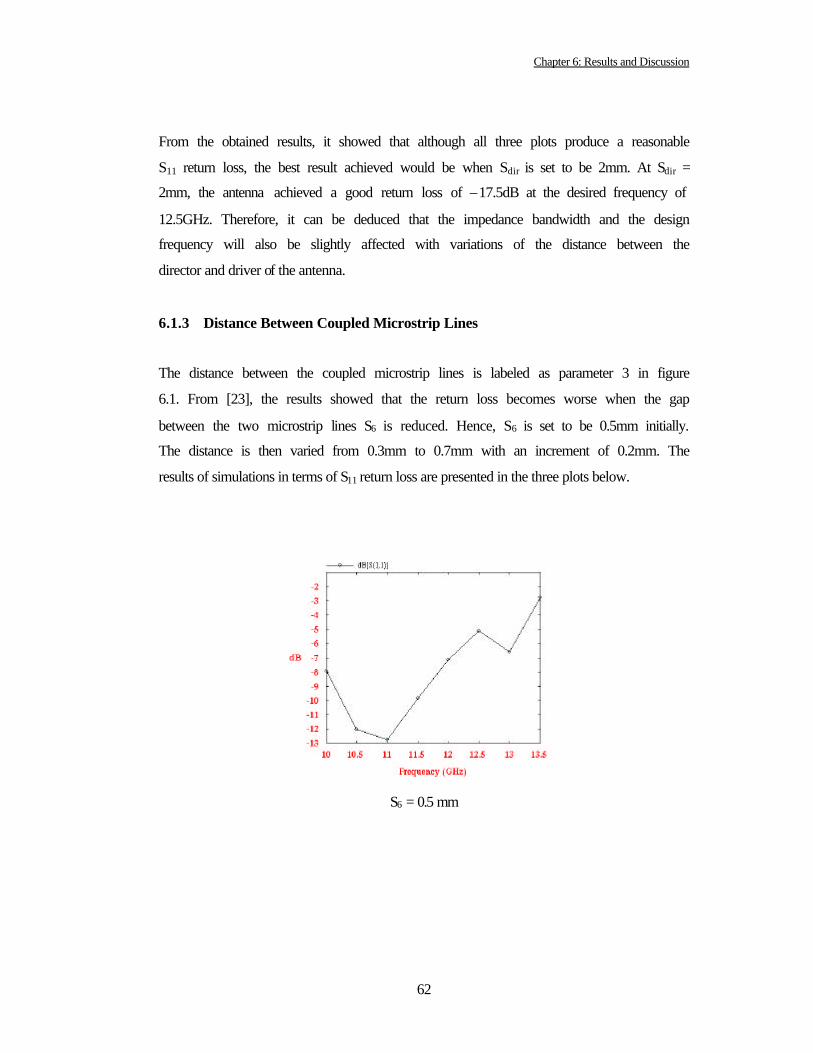
Chapter 6: Results and Discussion
62
From the obtained results, it showed that although all three plots produce a reasonable
S11 return loss, the best result achieved would be when Sdir is set to be 2mm. At Sdir =
2mm, the antenna achieved a good return loss of –17.5dB at the desired frequency of
12.5GHz. Therefore, it can be deduced that the impedance bandwidth and the design
frequency will also be slightly affected with variations of the distance between the
director and driver of the antenna.
6.1.3 Distance Between Coupled Microstrip Lines
The distance between the coupled microstrip lines is labeled as parameter 3 in figure
6.1. From [23], the results showed that the return loss becomes worse when the gap
between the two microstrip lines S6 is reduced. Hence, S6 is set to be 0.5mm initially.
The distance is then varied from 0.3mm to 0.7mm with an increment of 0.2mm. The
results of simulations in terms of S11 return loss are presented in the three plots below.
S6 = 0.5 mm

Chapter 6: Results and Discussion
63
S6 = 0.3 mm
S6 = 0.7 mm
After analyzing the three obtained plots, it can be assumed that the return loss would
degrades with increasing distance between the coupled microstrip lines. When S6 is set
at 0.7mm, the return loss achieved is only –9dB at 11GHz. However, when S6 is set at
0.3mm, the antenna obtained a very good return loss of –21dB at 10.5GHz. Although
the centre frequency is not achieved at the desired frequency of 12.5GHz, variations to
other parameters should be able to solve this problem. Therefore, it can be deduced that
the return loss would be most desirable when the distance between the coupled
microstrip lines is set at 0.3mm.

Chapter 6: Results and Discussion
64
6.1.4 Length of Driver
The next parameter to investigate is the length of the driver which is labeled as
parameter 4 in figure 6.1. From [23], it stated that the length of the driver Ldri is
optimum when it is about a guide wavelength. Therefore, from chapter 5, the value of
Ldri is calculated to be 9.17mm, which is equal to the guide wavelength of the antenna.
The length of the driver is then varied from 8.17mm to 10.17mm with an increment of
1mm. The results of simulations in terms of S11 return loss are presented in the three
plots below.
Ldri = 9.17 mm
Ldri = 10.17 mm

Chapter 6: Results and Discussion
65
Ldri = 8.17 mm
From the three graphs shown above, it can be observed that all the plots are able to
achieve a centre frequency of 12.5GHz, which is the desired frequency for the design.
In addition, in terms of return loss, all three plots also provide reasonable values of
return losses. However, when Ldri is set to 8.17mm, the antenna is able to achieve an
extremely good return loss of –27dB and a very wide bandwidth. Hence, it can be
deduced that in order to achieve good return loss and wide bandwidth, it is necessary for
the length of the driver to be less than the guide wavelength, most preferably about
1mm less than λG.
6.1.5 Distance From the Driver to the Reflector
The last parameter to investigate is the distance from the driver to the reflector, labeled
as parameter 5 in figure 6.1. From [23], it showed that the best result could be obtain if
the distance from the driver to the reflector Sref is about a quarter guide wavelength.
Thus, as shown in chapter 5, the value of Sref is calculated to be 2.29mm, which is
equivalent to a quarter guide wavelength. The distance is then varied from 1.29mm to
3.29mm with an increment of 1mm. The results of simulations in terms of S11 return
loss are presented in the three plots in the following page.

Chapter 6: Results and Discussion
66
Sref = 2.29 mm
Sref = 1.29 mm
Sref = 3.29 mm

Chapter 6: Results and Discussion
67
After analyzing the results, it can be observed that the deductions from [23] can also be
applicable to this design. From the plots, it can be seem that the best result is achieved
when Sref is set to be 2.29mm, which is equivalent to a quarter guide wavelength. The
return loss is excellent and it also produces a very wide bandwidth. Therefore, for the
last parameter, it can be considered a very sensitive parameter of the Quasi-Yagi
antenna as it affects both the antenna’s design frequency and its operational bandwidth.
6.1.6 Final Design
As a result of the investigations on the sensitivity analysis of the Quasi Yagi antenna,
the following dimensions have been determined for an antenna with relative dielectric
constant of 10.2, substrate thickness of 0.635mm and a design frequency of 12.5GHz.
Length of Director = 3.8mm
Distance between Director and Driver = 2mm
Distance between Coupled Microstrip Lines = 0.3mm
Length of Driver = 8.17mm
Distance from Driver to Reflector = 2.29mm
Shown below is the final design of the Quasi-Yagi antenna drawn on IE3D.
Figure 6.2: Schematic Diagram of Quasi-Yagi antenna from IE3D
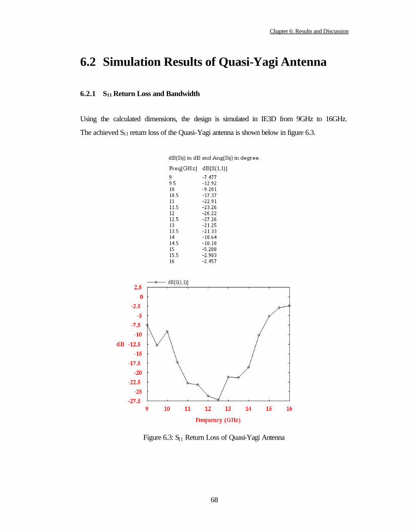
Chapter 6: Results and Discussion
68
6.2 Simulation Results of Quasi-Yagi Antenna
6.2.1 S11 Return Loss and Bandwidth
Using the calculated dimensions, the design is simulated in IE3D from 9GHz to 16GHz.
The achieved S11 return loss of the Quasi-Yagi antenna is shown below in figure 6.3.
Figure 6.3: S11 Return Loss of Quasi-Yagi Antenna

Chapter 6: Results and Discussion
69
From the gathered results, it can be seen that the return loss is about –27.26dB at the
design frequency of 12.5GHz, which can be considered acceptable. As for the
bandwidth of the antenna, it is defined as the frequency range over which S11 is less
than or equal to –10dB. The bandwidth can be calculated using the following equation:
where f0 is the centre frequency or the frequency where S11 is minimum
f1 and f2 are the frequencies at which S11 equals –10dB
Applying the above-mentioned equation, the calculated bandwidth of the Quasi-Yagi
antenna is approximately about 36%. This accomplishment can be considered
satisfactory, as the primary objective of achieving wide bandwidth at high frequencies
for the Quasi-Yagi antenna has been met.
6.2.2 Voltage Standing-Wave Ratio
As for the Voltage Standing-Wave Ratio (VSWR), it is defined as a measurement of the
mismatch between the load and the transmission line. Therefore, the simulated VSWR
for the design of the Quasi-Yagi antenna is shown below in figure 6.4.
%100)(
0
12 xf
ffBW
−=

Chapter 6: Results and Discussion
70
Figure 6.4: Simulated VSWR of the Quasi-Yagi Antenna
From the plot, it can be seen that VSWR < 2 at about 10.5GHz - 14.5GHz. This result
showed that between the range of 10.5GHz and 14.5GHz, the VSWR of the antenna can
be considered desirable as it is less than 2. However, when the design frequency is
increased from 15GHz onwards, the VSWR tends to become worse, as can be seen from
the plot. In other words, the line and the load tend to become more mismatched as the
design frequency is increased from 15GHz onwards.
6.2.3 Impedance Smith Chart and Average Current Density
Figure 6.5: Impedance Smith Chart of Quasi-Yagi Antenna

Chapter 6: Results and Discussion
71
Figure 6.5 on the previous page shows the impedance smith chart obtained for the
Quasi-Yagi antenna. For the plot, it shows that most of the points are located at the
middle of the circle. Hence, this indicates that the matching of this antenna is quite
good, as the desired location of the points should be in the middle of the circle (50Ω). In
addition, the average current density of the antenna at 12.5GHz is shown in figure 6.6
below.
Figure 6.6: Average Current Density at 12.5GHz.

Chapter 6: Results and Discussion
72
6.2.4 Radiation Patterns of Quasi-Yagi Antenna
Figure 6.7: 2D Polar Pattern of Quasi-Yagi Antenna
Figure 6.8: 2D Radiation Pattern of Quasi-Yagi Antenna

Chapter 6: Results and Discussion
73
Figure 6.9: 3D Radiation pattern of Quasi-Yagi Antenna

Chapter 6: Results and Discussion
74
Figure 6.10: 3D Mapped Pattern of Quasi-Yagi Antenna
Figures 6.7 - 6.10 in the previous pages are the radiation patterns achieved by the Quasi-
Yagi antenna at the design frequency of 12.5GHz. The values shown above are the
radiation parameters of the antenna obtained at 12.5GHz.

75
CHAPTER 7 SUMMARY AND FUTURE PROSPECTS This chapter concludes with a summary for the work done for this thesis and the future
prospects of the Quasi-Yagi antenna and the Linearly Tapered Slot antenna. A run-
down on the topics covered during this thesis is presented, including a sensitivity
analysis on the Quasi-Yagi antenna. Subsequently, the future prospects of microstrip
antennas, especially broadband planar antennas, have been addressed.
7.1 Summary
Microstrip antennas have been receiving much attention over the past few years due to
its many conventional valuable properties like low-profile, light-weight, robust and

Chapter 7: Summary and Future Prospects
76
reasonably cheap to manufacture. As a result, microstrip antennas have been used
extensively in microwave systems and wireless communication applications. Although
the microstrip antenna suffers from some serious drawbacks like narrow frequency
bandwidth and low efficiency, the performance of microstrip antenna elements and
arrays has been constantly enhanced through the years. Many different forms of
microstrip antennas have been developed over the years and in this thesis, two types of
broadband planar antennas have been analyzed for used in spatial power combining.
In this thesis, both the Quasi-Yagi antenna and the Linearly Tapered Slot antenna have
been analyzed both theoretically and experimentally through computer simulations.
Detailed characteristics of the two types of antennas are presented, including their
advantages, disadvantages and individual radiation characteristics. In addition, the
design procedures for both the planar antennas were also investigated and presented. In
chapter 5, the design guidelines and considerations for both the antennas have been
shown, including all the calculations for both the antennas’ dimensions. The antennas
are to be fabricated with a high dielectric constant substrate material (Duroid with
dielectric constant ε r) with substrate thickness of 0.635mm.
On the other hand, a sensitivity analysis of the Quasi-Yagi antenna has been performed
for a substrate of dielectric constant of 10.2 and thickness of 0.635mm at the design
frequency of 12.5GHz. The effects of the five parameters on its operational frequency
and impedance bandwidth are investigated and the parameters most affecting the
performance of the antenna are also identified. The results of the analysis revealed that
all of the parameters would definitely affect the antennas’ performance in terms of
return loss and operational frequency. However, the most sensitive parameters would be
the length of the driver, director and the distance from the driver to the reflector. The
length of the driver should most preferably be 1mm less than the guide wavelength λG.
The length of the director should also be approximately half of the length of the driver.
Lastly, for the distance from the driver to the reflector, it should be about a quarter
guide wavelength. Comparing this observation to the results obtained in [23], it can be
seen that there are some dissimilarity in the sensitivity analysis of the Quasi-Yagi
antenna. The reason for the dissimilarity might be due to the difference in dielectric

Chapter 7: Summary and Future Prospects
77
constant and substrate thickness of the material used to fabricate the Quasi-Yagi
antenna.
Therefore, taking into account of the results of the sensitivity analysis, the full-wave
(MoM) method of moment analysis package IE3D of Zeland Software Inc. is used to
analyze the performance of the Quasi-Yagi antenna. The simulation results showed that
the antenna is able to achieve a simulated 36% frequency bandwidth for voltage
standing-wave ratio VSWR < 2 at the centre frequency of 12.5GHz. In addition, the
impedance smith chart showed an acceptable matched load to the transmission line. Last
but not least, the average current density, radiation patterns, radiation parameters
achieved at 12.5GHz are also presented.
As for the limitations encountered during the design process of the two antennas, the
analysis of Linearly Tapered Slot antennas can be considered very complex due to its
large size. As a result, the performance analysis of the LTSA is not done as the program
IE3D could not support such a large and complex structure. In addition, the simulations
for the Quasi-Yagi antenna have also been slow due to its complex structure and
numerous calculations involved. Despite that, a sensitivity analysis of the Quasi-Yagi
antenna has been performed and presented in this thesis.
7.2 Future Prospects
The microstrip antenna has been a huge phenomenon over the past few years. Although
much efforts have gone into researches on designing the microstrip antenna, there
appears to be no definite design procedures and formulations at present. The reason for
this is because of the homogeneous nature of the microstrip structure. In other words, it
is extremely difficult to analyze the electromagnetic fields generated by the microstrip
antenna. Although some analysis methods have been presented in this thesis, these
methods are not necessarily precise and might not achieve accurate results. Hence, it
would be ideal if the design strategy of microstrip antennas could be well documented

Chapter 7: Summary and Future Prospects
78
in the distant future so that microstrip antennas will eventually replace the large
conventional microwave antennas in most applications.
Both the Quasi-Yagi antenna and the Linearly Tapered Slot antenna have proven to be
an effective component for use in spatial power combining. Both the antennas possess
many attractive features such as wide bandwidth and end-fire radiation characteristics.
In addition, the Quasi-Yagi antenna also has a smaller size compared to the LTSA.
Thus, with further improvements and researches, both these antennas would be very
useful in applications like wireless communications systems, phased arrays, power
combining and millimeter-wave imaging arrays.

79
References
[1] T. C. Edwards, “Foundations for Microstrip Circuit Design,” John Wiley &
Sons, USA, 1981.
[2] M. E. Bialkowski, “Passive and Active Microwave Subsystems,” Lecture Notes,
University of Queensland, Dept. of Computer Science and Electrical Eng.,
Brisbane, 2000.
[3] I. J. Bahl and P. Bhartia, “Microstrip Antennas,” Artech House, Massachusetts,
1980.
[4] G. A. Deschamps, “Microstrip Microwave Antennas,” presented at 3rd USAR
Symposium on Antennas, 1953.
[5] H. Gutton and G. Baissinot, “Flat Aerial for Ultra High Frequencies,” French
Patent No. 703113, 1995.
[6] R. E. Munson, “Single Slot Cavity Antennas Assembly,” U.S. Patent No.
3713162, Jan 23, 1973.
[7] J. Q. Howell, “Microstrip Antennas,” IEEE Trans. on Antennas and
Propagation, Jan 1975, pp.90-93.
[8] J. R. James et al, “Microstrip Antenna Theory and Design,” IEE and Peter
Peregrinus, London and New York, 1981.
[9] Proc. Workshop on Printed Circuit Antenna Technology, Paper 31, New Mexico
State University, Las Cruces, Oct 1979, pp. 480.
[10] K. R. Carver and J.W. Mink, “Microstrip Antenna Technology,” IEEE Trans.
On Antennas and Propagation, Vol. AP-29, No. 1, Jan 1981, pp. 2-24.

80
[11] R. S. Hall et al, “Wide Bandwidth Microstrip Antenna for Circuit Integration,”
Electronics Letters, Vol. 15, No. 15, June 1979, pp. 458-460.
[12] J. R. James and P. S. Hall, “Handbook of Microstrip Antennas, Volume 1,” Peter
Peregrinus Ltd, London, 1989.
[13] C.A. Balanis, “Antenna Theory: Analysis and Design,” 2nd ed., John Wiley &
Sons, New York, 1997.
[14] K. C. Gupta et al, “Microstrip Lines and Slotlines,” Artech House, USA, 1979.
[15] J. R. James and P. S. Hall, “Handbook of Microstrip Antennas, Volume 2,” Peter
Peregrinus Ltd, London, 1989.
[16] N. Kaneda et al. “A Broad-Band Microstrip-to-Waveguide Transition Using
Quasi-Yagi Antenna,” IEEE Trans. Microwave Theory Tech., Vol. 47, No. 12,
Dec. 1999, pp.2562-2567.
[17] Y. Qian and T. Itoh, “A Broadband Uniplanar Microstrip-to-CPS Transition,”
Proc. Asia Pacific Microwave Conf., Vol. 2, City University of Hong Kong,
Dept. of Electronic Eng., Hong Kong, PRC, 1997, pp.609-612.
[18] Y. Qian et al. “A Uniplanar Quasi-Yagi Antenna with Wide Bandwidth and Low
Mutual Coupling Characteristics,” IEEE AP-S Int. Symp ., Vol. 2, Piscataway,
New Jersey, 1999, pp.924-927.
[19] W. R. Deal et al. “A New Quasi-Yagi Antenna for Planar Active Antenna
Arrays,” IEEE Trans. Microwave Theory Tech., Vol. 48, No. 6, June 2000,
pp.910-917.

81
[20] K. S. Yngvesson et al., “The Tapered Slot Antenna – A New Integrated Element
for Millimeter-Wave Applications,” IEEE Trans. Microwave Theory Tech., Vol
37, No. 2, Feb. 1989, pp.365-374.
[21] R. A. York and Z. B. Popovic, “Active and Quasi-optical Arrays for Solid-State
Power Combining,” Wiley, New York, 1997.
[22] R.N. Simons and R.Q. Lee, “Space Power Amplification with Actively Linearly
Tapered Slot Antenna Array,” IEEE MTT-S Int. Microwave Symp. Dig., Vol 2,
IEEE, New York, 1992, pp. 623-626.
[23] H. J. Song, M. E. Bialkowski and P.Kabacik, “Parameter Study of a Broadband
Uniplanar Quasi-Yagi Antenna,” MIKON – 2000.
[24] Y. Qian et al, “Microstrip-fed Quasi-Yagi Antenna with Broadband
Characteristics,” Electronics Letters, Vol. 34, No. 23, Nov. 1998, pp. 2194-
2196.
[25] Q. Wang and M. E. Bialkowski, “An Antipodal Tapered Slot Antenna on a High
Dielectric Constant Substrate,” Proc. APCC/ICCS98, Singapore, Nov. 1998, pp.
604-607.
[26] R.N. Simons, R.Q. Lee and T.D. Perl, “Non-Planar Linearly Tapered Slot
Antenna with Balanced Microstrip Feed,” IEEE AP-S Int. Symp., Vol 4, IEEE,
New York, N.Y., 1992, pp. 2109- 2112.

专注于微波、射频、天线设计人才的培养 易迪拓培训 网址:http://www.edatop.com
如 何 学 习 天 线 设 计
天线设计理论晦涩高深,让许多工程师望而却步,然而实际工程或实际工作中在设计天线时却很
少用到这些高深晦涩的理论。实际上,我们只需要懂得最基本的天线和射频基础知识,借助于 HFSS、
CST 软件或者测试仪器就可以设计出工作性能良好的各类天线。
易迪拓培训(www.edatop.com)专注于微波射频和天线设计人才的培养,推出了一系列天线设计培
训视频课程。我们的视频培训课程,化繁为简,直观易学,可以帮助您快速学习掌握天线设计的真谛,
让天线设计不再难…
HFSS 天线设计培训课程套装
套装包含 6 门视频课程和 1 本图书,课程从基础讲起,内容由浅入深,
理论介绍和实际操作讲解相结合,全面系统的讲解了 HFSS 天线设计的
全过程。是国内最全面、最专业的 HFSS 天线设计课程,可以帮助你快
速学习掌握如何使用 HFSS 软件进行天线设计,让天线设计不再难…
课程网址:http://www.edatop.com/peixun/hfss/122.html
CST 天线设计视频培训课程套装
套装包含 5 门视频培训课程,由经验丰富的专家授课,旨在帮助您从
零开始,全面系统地学习掌握 CST 微波工作室的功能应用和使用 CST
微波工作室进行天线设计实际过程和具体操作。视频课程,边操作边
讲解,直观易学;购买套装同时赠送 3 个月在线答疑,帮您解答学习
中遇到的问题,让您学习无忧。
详情浏览:http://www.edatop.com/peixun/cst/127.html
13.56MHz NFC/RFID 线圈天线设计培训课程套装
套装包含 4 门视频培训课程,培训将 13.56MHz 线圈天线设计原理和仿
真设计实践相结合,全面系统地讲解了 13.56MHz 线圈天线的工作原
理、设计方法、设计考量以及使用 HFSS 和 CST 仿真分析线圈天线的
具体操作,同时还介绍了 13.56MHz 线圈天线匹配电路的设计和调试。
通过该套课程的学习,可以帮助您快速学习掌握 13.56MHz 线圈天线及
其匹配电路的原理、设计和调试…
详情浏览:http://www.edatop.com/peixun/antenna/116.html

`
专注于微波、射频、天线设计人才的培养 易迪拓培训 网址:http://www.edatop.com
关于易迪拓培训:
易迪拓培训(www.edatop.com)由数名来自于研发第一线的资深工程师发起成立,一直致力和专注
于微波、射频、天线设计研发人才的培养;后于 2006 年整合合并微波 EDA 网(www.mweda.com),
现已发展成为国内最大的微波射频和天线设计人才培养基地,成功推出多套微波射频以及天线设计经
典培训课程和 ADS、HFSS 等专业软件使用培训课程,广受客户好评;并先后与人民邮电出版社、电
子工业出版社合作出版了多本专业图书,帮助数万名工程师提升了专业技术能力。客户遍布中兴通讯、
研通高频、埃威航电、国人通信等多家国内知名公司,以及台湾工业技术研究院、永业科技、全一电
子等多家台湾地区企业。
我们的课程优势:
※ 成立于 2004 年,10 多年丰富的行业经验
※ 一直专注于微波射频和天线设计工程师的培养,更了解该行业对人才的要求
※ 视频课程、既能达到了现场培训的效果,又能免除您舟车劳顿的辛苦,学习工作两不误
※ 经验丰富的一线资深工程师主讲,结合实际工程案例,直观、实用、易学
联系我们:
※ 易迪拓培训官网:http://www.edatop.com
※ 微波 EDA 网:http://www.mweda.com
※ 官方淘宝店:http://shop36920890.taobao.com