ecen689: special topics in optical interconnects circuits...
TRANSCRIPT
Sam PalermoAnalog & Mixed-Signal Center
Texas A&M University
ECEN689: Special Topics in Optical Interconnects Circuits and Systems
Spring 2016
Lecture 1: Introduction

Class Topics
• System and design issues relevant to high-speed optical interconnects
• Channel properties• Modeling, measurements, communication techniques
• Optical interconnect circuits• Drivers, receivers, equalizers, timing systems
• Optical interconnect system design• Modeling and performance metrics
• Optical interconnect system examples
2

Administrative
• Instructor:• Sam Palermo• 315E WERC Bldg., 845-4114, [email protected]• Office hours: MW 1:00pm-2:30pm
• Lectures: TR 2:20pm-3:35pm, C E 007
• Class web page• http://www.ece.tamu.edu/~spalermo/ecen689_oi.html
3
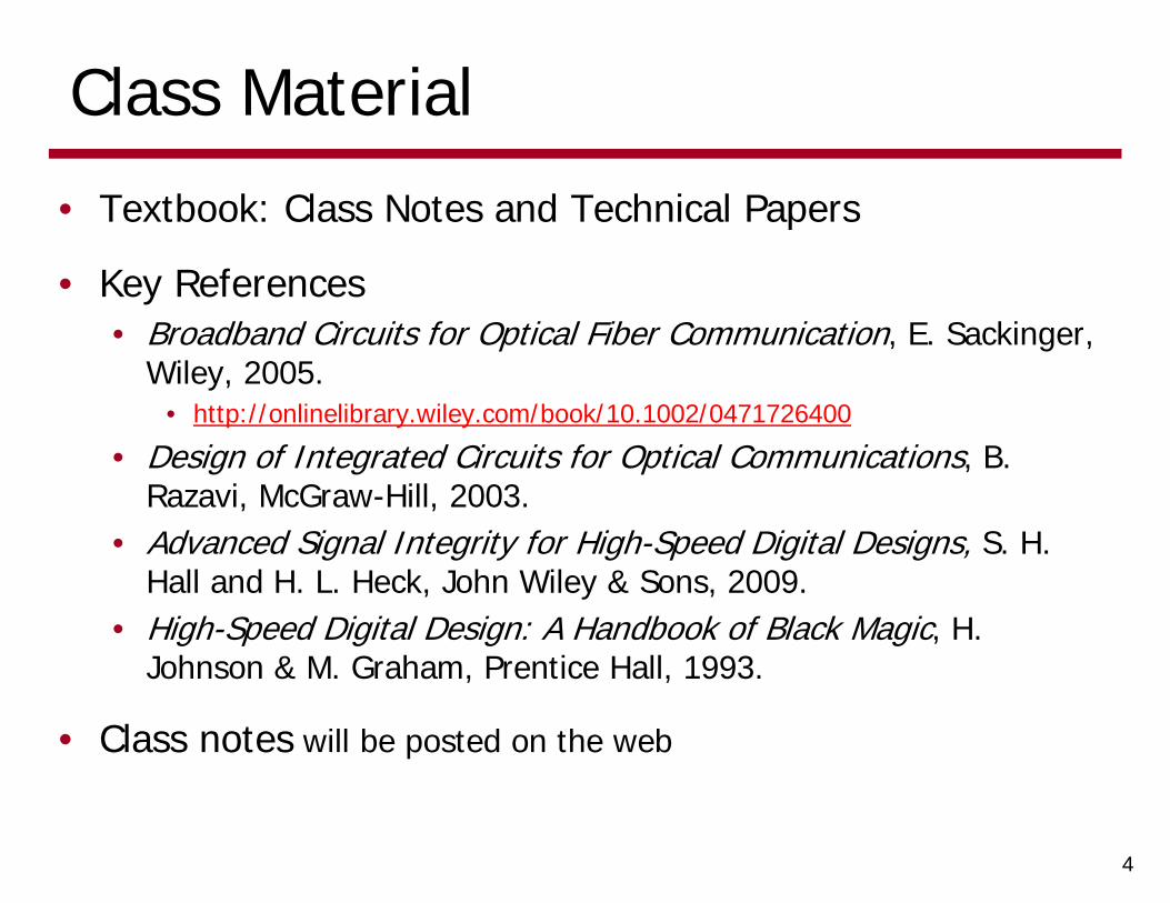
Class Material
• Textbook: Class Notes and Technical Papers
• Key References• Broadband Circuits for Optical Fiber Communication, E. Sackinger,
Wiley, 2005.• http://onlinelibrary.wiley.com/book/10.1002/0471726400
• Design of Integrated Circuits for Optical Communications, B. Razavi, McGraw-Hill, 2003.
• Advanced Signal Integrity for High-Speed Digital Designs, S. H. Hall and H. L. Heck, John Wiley & Sons, 2009.
• High-Speed Digital Design: A Handbook of Black Magic, H. Johnson & M. Graham, Prentice Hall, 1993.
• Class notes will be posted on the web
4

Grading
• Exams (50%)• Two midterm exams (25% each)
• Homework (20%)• Collaboration is allowed, but independent simulations and write-ups• Need to setup CADENCE simulation environment• Due at beginning of lab or 5PM (HW)• No late homework will be graded
• Final Project (30%)• Groups of 1-2 students• Report and PowerPoint presentation required
5
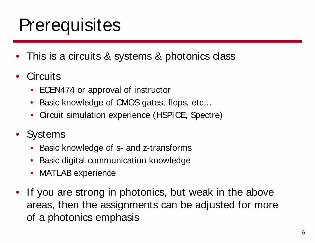
Prerequisites
• This is a circuits & systems & photonics class
• Circuits• ECEN474 or approval of instructor• Basic knowledge of CMOS gates, flops, etc…• Circuit simulation experience (HSPICE, Spectre)
• Systems• Basic knowledge of s- and z-transforms• Basic digital communication knowledge• MATLAB experience
• If you are strong in photonics, but weak in the above areas, then the assignments can be adjusted for more of a photonics emphasis
6

Simulation Tools
• Matlab
• ADS (Statistical BER link analysis)
• Cadence
• 90nm CMOS device models• Can use other technology models if they are a
90nm or more advanced CMOS node
• Other tools, schematic, layout, etc… are optional
7

8
Preliminary Schedule
• Dates may change with reasonable notice

Optical Interconnects
• Electrical Channel Issues• Optical Channel• Optical Transmitter Technology• Optical Receiver Technology• Optical Integration Approaches
9

High-Speed Electrical Link System
10

11
Channel Performance Impact

Link with Equalization
12
Seria
lizer
Des
eria
lizer

13
Channel Performance Impact

High-Speed Optical Link System
14
Optical Channel• Optical interconnects remove many channel limitations• Reduced complexity and power
consumption• Potential for high information density with
wavelength-division multiplexing (WDM)

Wavelength-Division Multiplexing
15
• WDM allows for multiple high-bandwidth (10+Gb/s) signals to be packed onto one optical channel
[Young JSSC 2010]

Optical Interconnects
• Electrical Channel Issues• Optical Channel• Optical Transmitter Technology• Optical Receiver Technology• Optical Integration Approaches
16
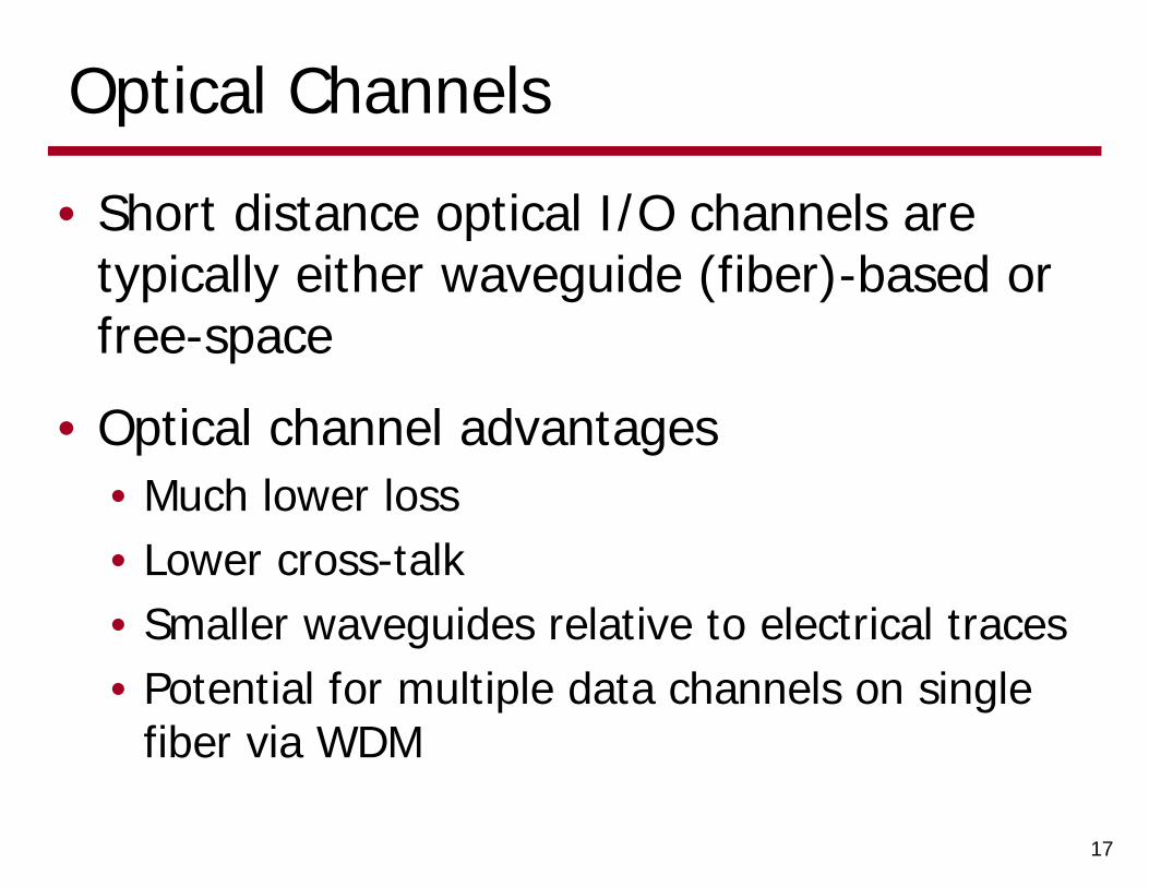
Optical Channels
• Short distance optical I/O channels are typically either waveguide (fiber)-based or free-space
• Optical channel advantages• Much lower loss• Lower cross-talk• Smaller waveguides relative to electrical traces• Potential for multiple data channels on single
fiber via WDM
17

Waveguide (Fiber)-Based Optical Links
• Optical fiber loss is specified in dB/km• Single-Mode Fiber loss
~0.25dB/km at 1550nm• RF coaxial cable loss ~100dB/km
at 10GHz
• Frequency dependent loss is very small• <0.5dB/km over a bandwidth
>10THz
• Bandwidth may be limited by dispersion (pulse-spreading)• Important to limit laser linewidth
for long distances (>1km)
18
Optical Fiber Cross-Section
Single-Mode Fiber Loss & Dispersion
[Sackinger]
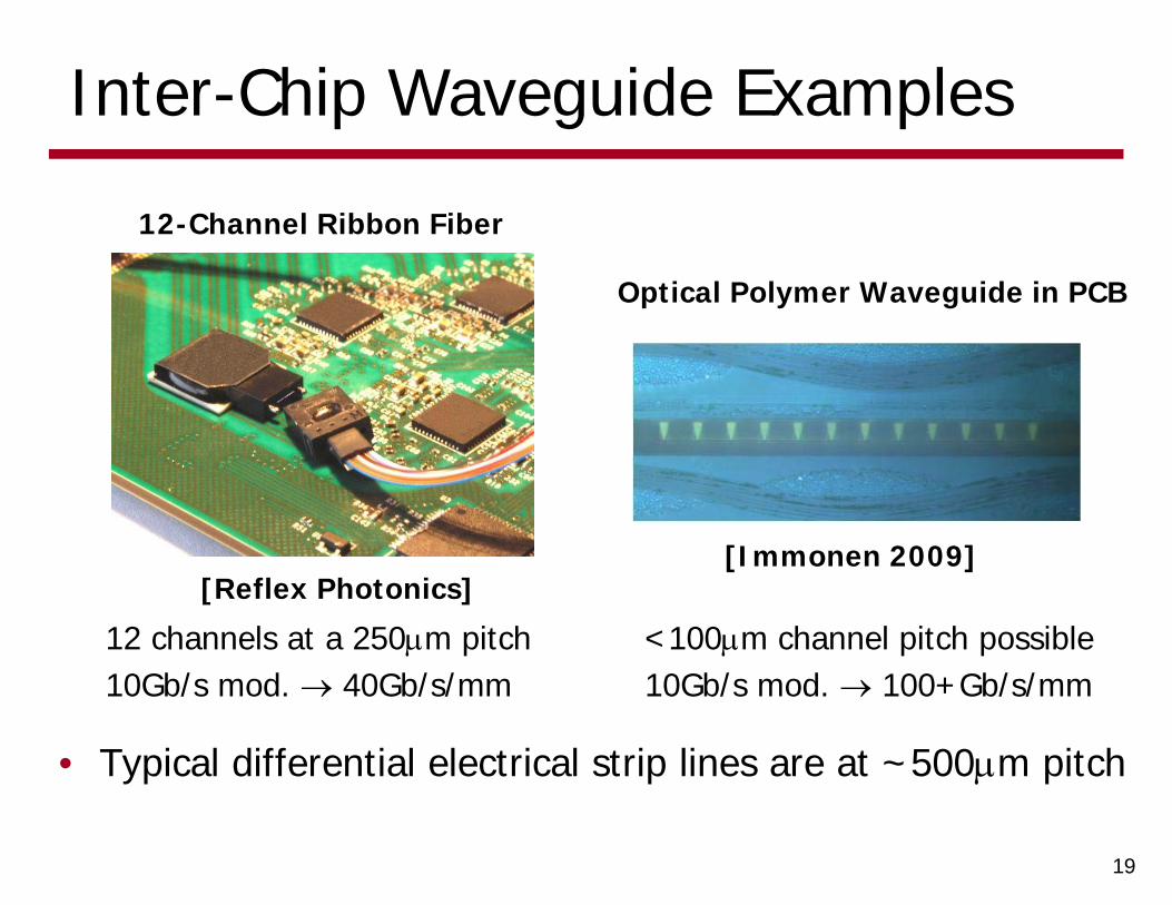
Inter-Chip Waveguide Examples
19
• Typical differential electrical strip lines are at ~500m pitch
12-Channel Ribbon Fiber
Optical Polymer Waveguide in PCB
[Reflex Photonics][Immonen 2009]
12 channels at a 250m pitch10Gb/s mod. 40Gb/s/mm
<100m channel pitch possible10Gb/s mod. 100+Gb/s/mm

Free-Space Optical Links
• Free-space (air or glass) interconnect systems have also been proposed
• Optical imaging system routes light chip-to-chip
20
[Gruber]

CMOS Waveguides – Bulk CMOS
• Waveguides can be made in a bulk process with a polysilicon core surrounded by an SiO2 cladding
• However, thin STI layer means a significant portion of the optical mode will leak into the Si substrate, causing significant loss (1000dB/cm)
• Significant post-processing is required for reasonable loss (10dB/cm) waveguides in a bulk process
21[Holzwarth CLEO 2008]

CMOS Waveguides – SOI
• SOI processes have thicker buried oxide layers to sufficiently confine the optical mode
• Allows for low-loss waveguides
22
[Narasimha JSSC 2007]

CMOS Waveguides – Back-End Processing
• Waveguides & optical devices can be fabricated above metallization
• Reduces active area consumption
• Allows for independent optimization of transistor and optical device processes
23
[Young JSSC 2010]
Optical Interconnects
• Electrical Channel Issues• Optical Channel• Optical Transmitter Technology• Optical Receiver Technology• Optical Integration Approaches
24

Optical Modulation Techniques
• Due to it’s narrow frequency (wavelength) spectrum, a single-longitudinal mode (SLM) laser source often generates the optical power that is modulated for data communication• This is required for long-haul (multi-km) communication• May not be necessary for short distance (~100m) chip-to-chip I/Os
• Two modulation techniques• Direct modulation of laser• External modulation of continuous-wave (CW) “DC” laser with
absorptive or refractive modulators
25

• Directly modulating laser output power• Simplest approach• Introduces laser “chirp”, which is unwanted frequency
(wavelength) modulation• This chirp causes unwanted pulse dispersion when passed
through a long fiber
Directly Modulated Laser
26

• External modulation of continuous-wave (CW) “DC” laser with absorptive or refractive modulators• Adds an extra component• Doesn’t add chirp, and allows for a transform limited
spectrum
Externally Modulated Laser
27
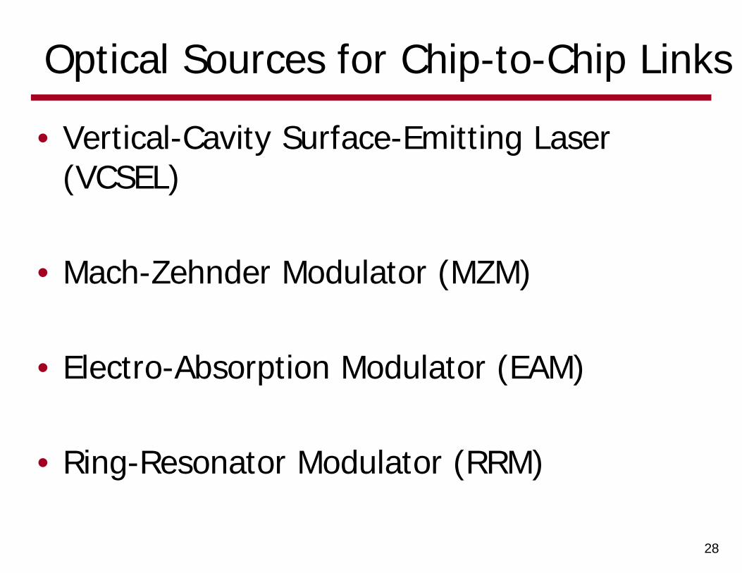
Optical Sources for Chip-to-Chip Links
• Vertical-Cavity Surface-Emitting Laser (VCSEL)
• Mach-Zehnder Modulator (MZM)
• Electro-Absorption Modulator (EAM)
• Ring-Resonator Modulator (RRM)
28

Vertical-Cavity Surface-Emitting Laser (VCSEL)
• VCSEL emits light perpendicular from top (or bottom) surface
• Important to always operate VCSEL above threshold current, ITH, to prevent “turn-on delay” which results in ISI
• Operate at finite extinction ratio (P1/P0)
29
ITH = 700A = 0.37mW/mA
AW Efficiency Slope
IP
IIP THo
VCSEL Cross-Section VCSEL L-I-V Curves

VCSEL Bandwidth vs Reliability
30
THavg IIBW
37311
2j
ATk
E
ejAMTTF
10Gb/s VCSEL Frequency Response [1]
4
1BW
MTTF
• Mean Time to Failure (MTTF) is inversely proportional to current density squared
[2]
• Steep trade-off between bandwidth and reliability
1. D. Bossert et al, "Production of high-speed oxide confined VCSEL arrays for datacom applications," Proceedings of SPIE, 2002.2. M. Teitelbaum and K. Goossen, "Reliability of Direct Mesa Flip-Chip Bonded VCSEL’s," LEOS, 2004.

VCSEL Drivers
• Current-mode drivers often used due to linear L-I relationship
• Equalization can be added to extend VCSEL bandwidth for a given current density
31
S. Palermo and M. Horowitz, “High-Speed Transmitters in 90nm CMOS for High-Density Optical Interconnects," ESSCIRC, 2006.
Current-Mode VCSEL Driver VCSEL Driver w/ 4-tap FIR Equalization

Electro-Absorption Modulator (EAM)
• Absorption edge shifts with changing bias voltage due to the “quantum-confined Stark or Franz-Keldysh effect” & modulation occurs
• Modulators can be surface-normal devices or waveguide-based
• Maximizing voltage swing allows for good contrast ratio over a wide wavelength range
• Devices are relatively small and can be treated as lump-capacitance loads
• 10 – 500fF depending on device type32
QWAFEM Modulator*
*N. Helman et al, “Misalignment-Tolerant Surface-Normal Low-Voltage Modulator for Optical Interconnects," JSTQE, 2005.
Waveguide EAM [Liu]

Ring-Resonator Modulator (RRM)
• Refractive devices which modulate by changing the interference light coupled into the ring with the waveguide light
• Devices are relatively small (ring diameters < 20m) and can be treated as lumped capacitance loads (~10fF)
• Devices can be used in WDM systems to selectively modulate an individual wavelength or as a “drop” filter at receivers
33
Optical Device Performance from: I. Young, E. Mohammed, J. Liao, A. Kern, S. Palermo, B. Block, M. Reshotko, and P. Chang, “Optical I/O Technology for Tera-Scale Computing," ISSCC, 2009.

Wavelength Division Multiplexing w/ Ring Resonators
• Ring resonators can act as both modulators and add/drop filters to steer light to receivers or switch light to different waveguides
• Potential to pack >100 waveguides, each modulated at more than 10Gb/s on a single on-chip waveguide with width <1m (pitch ~4m)
34
[Rabus]

Ring-Resonator-Based Silicon Photonics Transceiver
35
• High-voltage drivers with simple pre-emphasis to extend bandwidth of silicon ring-resonator modulators
• Forwarded-clock receiver with adaptive power-sensitivity RX• Bias-based tuning loop to stabilize photonic device’s
resonance wavelength
[Li ISSCC 2013]

CMOS Modulator Driver• Simple CMOS-style
voltage-mode drivers can drive EAM and RRM due to their small size
• Device may require swing higher than nominal CMOS supply• Pulsed-Cascode driver can
reliably provide swing of 2xVdd (or 4xVdd) at up to 2FO4 data rate
36S. Palermo and M. Horowitz, “High-Speed Transmitters in 90nm CMOS for High-Density Optical Interconnects," ESSCIRC, 2006.
Pulsed-Cascode Driver

Mach-Zehnder Modulator (MZM)
• Refractive modulator which splits incoming light into two paths, induces a voltage-controlled phase shift in the two paths, and recombines the light in or out of phase
• Long device (several mm) requires driver to drive low-impedance transmission line at potentially high swing (5Vppd)
• While much higher power relative to RRM, they are less sensitive to temperature variations
37
[Analui]

Optical Interconnects
• Electrical Channel Issues• Optical Channel• Optical Transmitter Technology• Optical Receiver Technology• Optical Integration Approaches
38

Optical Receiver Technology
• Photodetectors convert optical power into current• p-i-n photodiodes• Integrated metal-semiconductor-
metal photodetector
• Electrical amplifiers then convert the photocurrent into a voltage signal• Transimpedance amplifiers• Limiting amplifiers• Integrating optical receiver
39

p-i-n Photodiode
• Normally incident light absorbed in intrinsic region and generates carriers
• Trade-off between capacitance and transit-time
• Typical capacitance between 100-300fF40
mA/mW108 5
pdpd
opt hcq
PI
Wpd e 1
Wvf sat
trdBPD
45.02
4.23
Responsivity:
Quantum Efficiency:
Transit-Time Limited Bandwidth:
[Sackinger]

Integrated Ge MSM Photodetector
41
SiO2
Cu
Ge
SiO2Silicon nitride
0.75 um
XSEM
Active area: < 2 um2Very low capacitance: <1 fF
Cu
SiN waveguide
2 um
Cu Cu
Ge
Detector
• Lateral Metal-Semiconductor-Metal (MSM Detector)• Silicon Nitride Waveguide-Coupled • Direct Germanium deposition on oxideI. Young, E. Mohammed, J. Liao, A. Kern, S. Palermo, B. Block, M. Reshotko, and P. Chang, “Optical I/O Technology for Tera-Scale Computing," IEEE Journal of Solid-State Circuits, 2010.

Optical Interconnects
• Electrical Channel Issues• Optical Channel• Optical Transmitter Technology• Optical Receiver Technology• Optical Integration Approaches
42
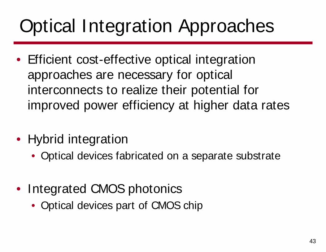
Optical Integration Approaches
• Efficient cost-effective optical integration approaches are necessary for optical interconnects to realize their potential for improved power efficiency at higher data rates
• Hybrid integration• Optical devices fabricated on a separate substrate
• Integrated CMOS photonics• Optical devices part of CMOS chip
43

Hybrid Integration
44
Wirebonding Flip-Chip Bonding
Short In-Package Traces
[Kromer] [Schow] [Mohammed]
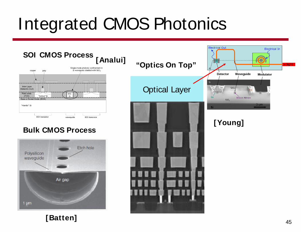
Integrated CMOS Photonics
45
Optical Layer
SOI CMOS Process
Bulk CMOS Process
“Optics On Top”[Analui]
[Batten]
[Young]

Future Photonic CMOS Chip
• Unified optical interconnect for on-chip core-to-core and off-chip processor-to-processor and processor-to-memory
46I. Young, E. Mohammed, J. Liao, A. Kern, S. Palermo, B. Block, M. Reshotko, and P. Chang, “Optical I/O Technology for Tera-Scale Computing," IEEE International Solid-State Circuits Conference, 2009.

Next Time
• Optical Channels• Sackinger Chapter 2
47