ecen 248 –introduction to digital systems design (spring...
TRANSCRIPT
ECEN 248 –Introduction to Digital Systems Design (Spring 2008)
(Sections: 501, 502, 503, 507)
Prof. Xi ZhangECE Dept, TAMU, 333N WERC
http://www.ece.tamu.edu/~xizhang/ECEN248

Programmable logic device (PLD)
A PLD is a general-purpose chip for implementing logic circuit. It contains a collection of logic circuit elements that can be customized in different ways. A PLD can be viewed as a “black box” that contains logic gates and programmable switches. The programmable switches allow the logic gates inside the PLD to be connected together to implement logic circuits.

Figure 3.24. Programmable logic device as a black box.
Logic gates and
programmableswitches
Inputs
(logic variables) Outputs
(logic functions)
Programmable logic device as a black box

Programmable logic devices
Different types of PLDSimple PLD (SPLD)
Programmable logic array (PLA)Programmable array logic (PAL)
Complex PLD (CPLD)Field-programmable gate arrays (FPGA)
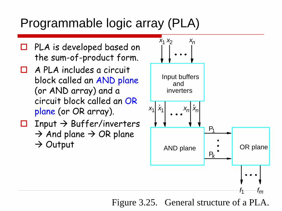
Figure 3.25. General structure of a PLA.f 1
AND plane OR plane
Input buffers
inverters and
P 1
P k
f m
x 1 x 2 x n
x 1 x 1 x n x n
Programmable logic array (PLA)
PLA is developed based on the sum-of-product form.A PLA includes a circuit block called an AND plane (or AND array) and a circuit block called an OR plane (or OR array).Input Buffer/inverters
And plane OR plane Output

Figure 3.26. Gate-level diagram of a PLA.f1
P1
P2
f2
x1 x2 x3
OR plane
Programmable
AND plane
connections
P3
P4
Gate-level diagram of a PLA
32131211 xxxxxxxf ++=
31321212 xxxxxxxf ++=
211 xxP =
312 xxP =
3213 xxxP =
314 xxP =
Output of And plane:
Output of OR plane:

Figure 3.27. Customary schematic for the PLA in Figure 3.26.f 1
P 1
P 2
f 2
x 1 x 2 x 3
OR plane
AND plane
P 3
P 4
Customary schematic for the PLA
32131211 xxxxxxxf ++=
31321212 xxxxxxxf ++=
211 xxP =
312 xxP =
3213 xxxP =
314 xxP =
Output of And plane:
Output of OR plane:

Programmable array logic (PAL) device
Programmable array logic (PAL) devicePAL is a programmable logic device similar to PLA. Difference between PLA and PAL
PLA: both AND plane and OR plane are programmable.PAL: Only AND plane is programmable, while OR plane is fixed.

Figure 3.28. An example of a PLA.
f 1
P 1
P 2
f 2
x 1 x 2 x 3
AND plane
P 3
P 4
An example of a PAL
Programmable fixed
OR plane
3211 xxxP =
3212 xxxP =
213 xxP =
3214 xxxP =
3213211 xxxxxxf +=
321212 xxxxxf +=

Comparison between PLA and PAL
Comparison between PLA and PALDrawbacks of PLA
PLA were hard to be implementedPLA reduced the speed performance of circuits.
Advantage of PALSimple to manufacturersLess expensiveBetter performance
Disadvantage of PALNot flexible as compared PLA, because OR plane is fixed.

Complex Programmable Logic Device (CPLDs)
SPLDs, including PLA, PAL, and etc, are useful for implementing a wide variety of small digital circuits.
CPLD are used to implement more sophisticated type of chip.

Complex Programmable Logic Device (CPLDs)
A CPLD comprises multiple circuit blocks on a single chip, with internal wiring resources to connect the circuit blocks. Each circuit block is similar to a PLA or a PALWe will refer to the circuit blocks as PAL-like blocks.
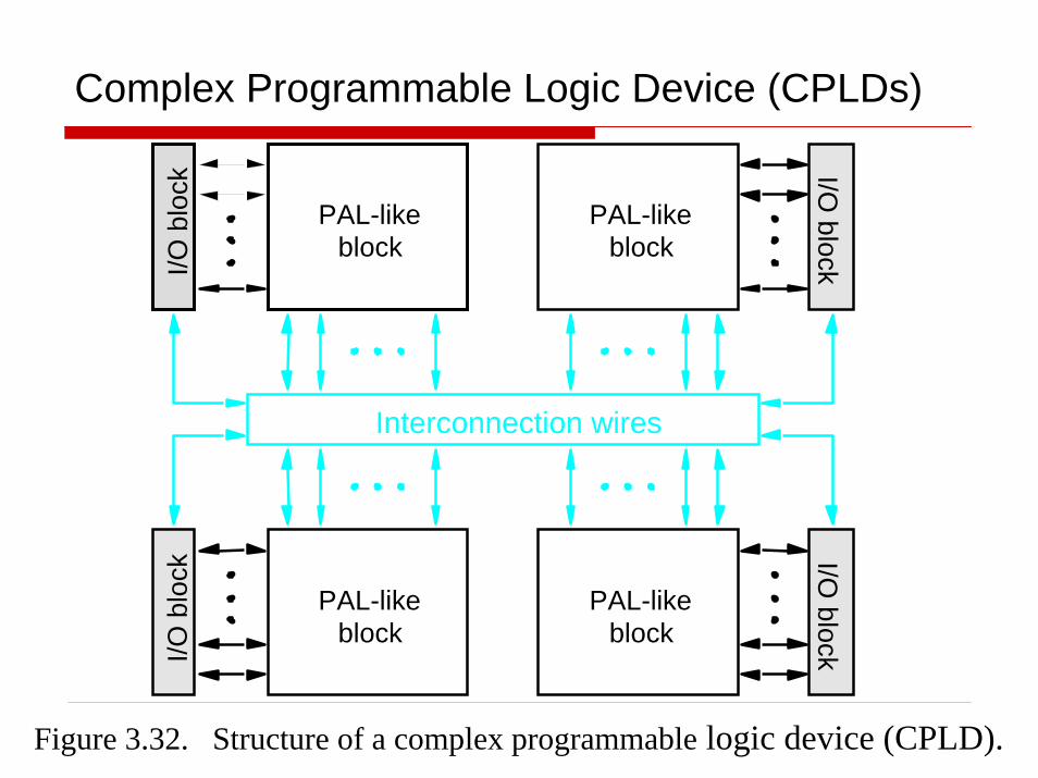
Figure 3.32. Structure of a complex programmable logic device (CPLD).
PAL-likeblock
I/O b
lock
PAL-like
block I/O
block
PAL-likeblock
I/O b
lock
PAL-likeblock
I/O block
Interconnection wires
Complex Programmable Logic Device (CPLDs)

Field-Programmable Gate Arrays (FPGA)
Larger and larger logic circuits need to accommodate in a single chip.One way to quantify a circuit’s size is to assume that the circuit is to be built using only simple logic gates and then estimate how many of these gates are needed. A commonly used measure is the total number of two-input NAND gates. This measure is often called the number of equivalent gates.By modern standards, a logic circuit with 10,000 gates is not large.

Field-Programmable Gate Arrays (FPGA)
FPGA is a programmable logic device that supports implementation of relatively large logic circuits. Not like CPLD, FPGAs do not contain AND or OR planes. Instead, FPGAs provide logic blocks for connecting to the pins of the package, and interconnection wires and switches.

General structure of an FPGA
The logic blocks are arranged in a two-dimensional array, depicted as hollow black box;The interconnection wires, depicted as solid blue box, are organized as horizontal and vertical routing channelsbetween rows and columns of logic blocks.Programmable connections also exist between I/O blocks and the interconnection wires.FPGA can implement circuit of more than a million equivalent gates in size.

Lookup Table (LUT)
Lookup table (LUT) is the most commonly used logic block in FPGA.A lookup table contains storage cells that are used to implement a small logic function.Each cell is capable of holding a single logic value, either 0 or 1.LUTs of various sizes may be created, where the size is defined by the number of inputs. LUTs are implemented by using multiplexers.
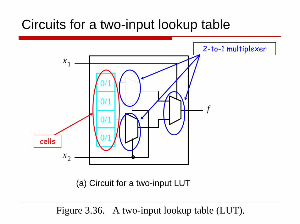
Figure 3.36. A two-input lookup table (LUT).
(a) Circuit for a two-input LUT
x 1
x 2
f
0/1
0/1
0/1
0/1
Circuits for a two-input lookup table
2-to-1 multiplexer
cells

Figure 3.36. A two-input lookup table (LUT).
0 0 1 1
0 1 0 1
1 0 0 1
x 1 x 2
(b) f 1 x 1 x 2 x 1 x 2 + =
f 1
(c) Storage cell contents in the LUT
x 1
x 2
1
0
0
1
f 1
Example of a two-input lookup table

Figure 3.37. A three-input LUT.
f
0/1
0/1
0/1
0/1
0/1
0/1
0/1
0/1
x 2
x 3
x 1
A three-input LUT
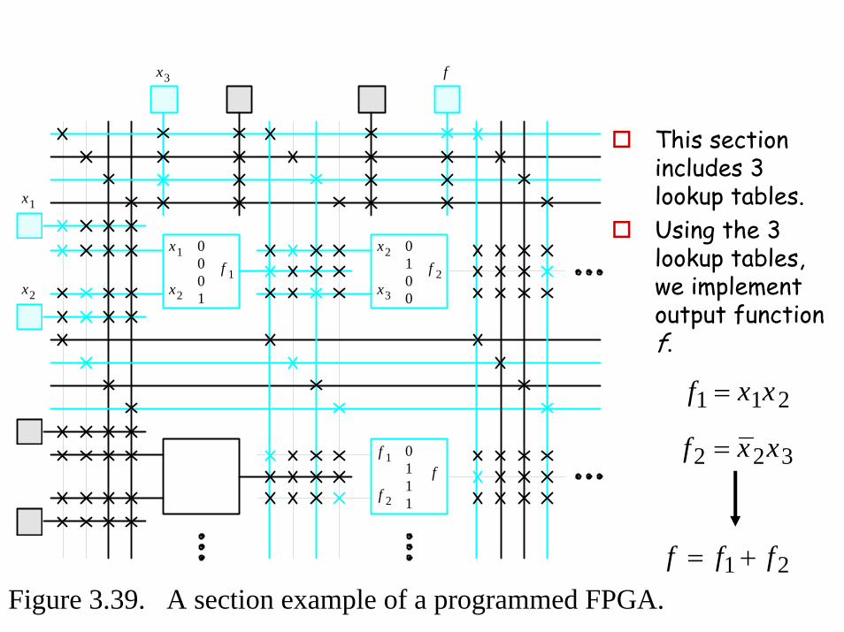
Figure 3.39. A section example of a programmed FPGA.
0 1 0 0
0 1 1 1
0 0 0 1
x 1
x 2
x 2
x 3
f 1
f 2
f 1 f 2
f
x 1
x 2
x 3 f
This section includes 3 lookup tables.Using the 3 lookup tables, we implement output function f.
211 xxf =
322 xxf =
21 fff +=