dspic33f product overview - microchip...
TRANSCRIPT

© 2005 Microchip Technology Inc. Preliminary DS70155C
dsPIC33FProduct Overview
dsPIC® DSC High-Performance 16-BitDigital Signal Controllers
Note the following details of the code protection feature on Microchip devices:
• Microchip products meet the specification contained in their particular Microchip Data Sheet.
• Microchip believes that its family of products is one of the most secure families of its kind on the market today, when used in the intended manner and under normal conditions.
• There are dishonest and possibly illegal methods used to breach the code protection feature. All of these methods, to our knowledge, require using the Microchip products in a manner outside the operating specifications contained in Microchip’s Data Sheets. Most likely, the person doing so is engaged in theft of intellectual property.
• Microchip is willing to work with the customer who is concerned about the integrity of their code.
• Neither Microchip nor any other semiconductor manufacturer can guarantee the security of their code. Code protection does not mean that we are guaranteeing the product as “unbreakable.”
Code protection is constantly evolving. We at Microchip are committed to continuously improving the code protection features of ourproducts. Attempts to break Microchip’s code protection feature may be a violation of the Digital Millennium Copyright Act. If such actsallow unauthorized access to your software or other copyrighted work, you may have a right to sue for relief under that Act.
Information contained in this publication regarding deviceapplications and the like is provided only for your convenienceand may be superseded by updates. It is your responsibility toensure that your application meets with your specifications.MICROCHIP MAKES NO REPRESENTATIONS OR WAR-RANTIES OF ANY KIND WHETHER EXPRESS OR IMPLIED,WRITTEN OR ORAL, STATUTORY OR OTHERWISE,RELATED TO THE INFORMATION, INCLUDING BUT NOTLIMITED TO ITS CONDITION, QUALITY, PERFORMANCE,MERCHANTABILITY OR FITNESS FOR PURPOSE.Microchip disclaims all liability arising from this information andits use. Use of Microchip’s products as critical components inlife support systems is not authorized except with expresswritten approval by Microchip. No licenses are conveyed,implicitly or otherwise, under any Microchip intellectual propertyrights.
DS70155C-page ii Prelimin
Trademarks
The Microchip name and logo, the Microchip logo, Accuron, dsPIC, KEELOQ, microID, MPLAB, PIC, PICmicro, PICSTART, PRO MATE, PowerSmart, rfPIC, and SmartShunt are registered trademarks of Microchip Technology Incorporated in the U.S.A. and other countries.
AmpLab, FilterLab, Migratable Memory, MXDEV, MXLAB, PICMASTER, SEEVAL, SmartSensor and The Embedded Control Solutions Company are registered trademarks of Microchip Technology Incorporated in the U.S.A.
Analog-for-the-Digital Age, Application Maestro, dsPICDEM, dsPICDEM.net, dsPICworks, ECAN, ECONOMONITOR, FanSense, FlexROM, fuzzyLAB, In-Circuit Serial Programming, ICSP, ICEPIC, Linear Active Thermistor, MPASM, MPLIB, MPLINK, MPSIM, PICkit, PICDEM, PICDEM.net, PICLAB, PICtail, PowerCal, PowerInfo, PowerMate, PowerTool, rfLAB, rfPICDEM, Select Mode, Smart Serial, SmartTel, Total Endurance and WiperLock are trademarks of Microchip Technology Incorporated in the U.S.A. and other countries.
SQTP is a service mark of Microchip Technology Incorporated in the U.S.A.
All other trademarks mentioned herein are property of their respective companies.
© 2005, Microchip Technology Incorporated, Printed in the U.S.A., All Rights Reserved.
Printed on recycled paper.
ary © 2005 Microchip Technology Inc.
Microchip received ISO/TS-16949:2002 quality system certification for its worldwide headquarters, design and wafer fabrication facilities in Chandler and Tempe, Arizona and Mountain View, California in October 2003. The Company’s quality system processes and procedures are for its PICmicro® 8-bit MCUs, KEELOQ® code hopping devices, Serial EEPROMs, microperipherals, nonvolatile memory and analog products. In addition, Microchip’s quality system for the design and manufacture of development systems is ISO 9001:2000 certified.

dsPIC33FdsPIC33F High-Performance 16-Bit
Digital Signal Controller Product Overview
Operating Range• DC – 40 MIPS (40 MIPS @ 3.0-3.6V, -40° to +85°C)• Industrial temperature range (-40° to +85°C)
High-Performance DSC CPU• Modified Harvard architecture• C compiler optimized instruction set• 16-bit wide data path
• 24-bit wide instructions• Linear program memory addressing up to 4M
instruction words• Linear data memory addressing up to 64 Kbytes
• 84 base instructions: mostly 1 word/1 cycle• Sixteen 16-bit general purpose registers• Two 40-bit accumulators:
- With rounding and saturation options• Flexible and powerful addressing modes:
- Indirect, modulo and bit-reversed
• Software stack• 16 x 16 fractional/integer multiply operations• 32/16 and 16/16 divide operations
• Single-cycle multiply-and-accumulate:- Accumulator write back for DSP operations- Dual data fetch
• Up to +/- 16-bit shifts, for up to 40-bit data
Direct Memory Access (DMA)• 8-channel hardware DMA
• Allows data transfer between RAM and a peripheral while CPU is executing code (no cycle stealing)
• 2 KB of dual-ported DMA buffer area (DMA RAM) to store data transferred via DMA
• Most peripherals support DMA
Interrupt Controller• 5-cycle latency• 117 interrupt vectors• Up to 67 available interrupt sources, up to
5 external interrupts• 7 programmable priority levels
• 5 processor exceptions
Digital I/O• Up to 85 programmable digital I/O pins• Wake-up/Interrupt-on-Change on up to 24 pins• Output pins can drive from 3.0V to 3.6V
• All digital input pins are 5V tolerant• 4 mA sink and source on all I/O pins
On-Chip Flash and SRAM• Flash program memory, up to 256 Kbytes• Data SRAM (up to 30 Kbytes):
- Includes 2 KB of DMA RAM
System Management• Flexible clock options:
- External, crystal, resonator, internal RC
- Fully integrated PLL- Extremely low jitter PLL
• Power-up timer
• Oscillator Start-up Timer/Stabilizer• Watchdog timer with its own RC oscillator• Fail-Safe Clock Monitor
• Reset by multiple sources
Power Management• On-chip 2.5V voltage regulator
• Switch between clock sources in real time• Idle, Sleep and Doze modes with fast wake-up
© 2005 Microchip Technology Inc. Preliminary DS70155C-page 1

dsPIC33F
Timers/Capture/Compare/PWM• Timer/Counters: up to nine 16-bit timers:
- Can pair up to make four 32-bit timers- 1 timer runs as Real-Time Clock with external
32 kHz oscillator- Programmable prescaler
• Input Capture (up to 8 channels):- Capture on up, down or both edges- 16-bit capture input functions
- 4-deep FIFO on each capture• Output Compare (up to 8 channels):
- Single or Dual 16-Bit Compare mode
- 16-Bit Glitchless PWM mode
Communication Modules• 3-wire SPI™ (up to 2 modules):
- Framing supports I/O interface to simple codecs
- Supports 8-bit and 16-bit data- Supports all serial clock formats and
sampling modes- 8-word FIFO buffers
• I2C™ (up to 2 modules):- Full Multi-Master Slave mode support- 7-bit and 10-bit addressing
- Bus collision detection and arbitration- Integrated signal conditioning- Address masking
• UART (up to 2 modules):- Interrupt-on-address bit detect- Wake-up-on-Start bit from Sleep mode
- 4-character TX and RX FIFO buffers- LIN bus support- IrDA® encoding and decoding in hardware
- High-Speed Baud mode• Data Conversion Interface (DCI) module:
- Codec interface
- Supports I2S and AC’97 protocols- Up to 16-bit data words, up to 16 words per
frame- 4-word deep TX and RX buffers
• Enhanced CAN 2.0B active (up to 2 modules):
- Up to 8 transmit and up to 16 receive buffers - 16 receive filters and 3 masks- Loopback, Listen Only and Listen All
Messages modes for diagnostics and bus monitoring
- Wake-up on CAN message- FIFO mode using DMA
Motor Control Peripherals• Motor Control PWM (up to 8 channels):
- 4 duty cycle generators- Independent or Complementary mode
- Programmable dead time and output polarity- Edge or center-aligned- Manual output override control
- Up to 2 Fault inputs- Trigger for A/D conversions- PWM frequency for 16-bit resolution
(@ 40 MIPS) = 1220 Hz for Edge-Aligned mode, 610 Hz for Center-Aligned mode
- PWM frequency for 11-bit resolution(@ 40 MIPS) = 39.1 kHz for Edge-Aligned mode, 19.55 kHz for Center-Aligned mode
• Quadrature Encoder Interface module:- Phase A, Phase B and index pulse input- 16-bit up/down position counter
- Count direction status- Position Measurement (x2 and x4) mode- Programmable digital noise filters on inputs
- Alternate 16-bit Timer/Counter mode- Interrupt on position counter rollover/
underflow
Analog-to-Digital Converters• Up to two 10-bit or 12-bit A/D modules in a device• 10-bit 2.2 Msps or 12-bit 1 Msps conversion:
- 2 or 4 simultaneous samples
- Up to 32 input channels with auto-scanning- 16-deep result buffer- Conversion start can be manual or
synchronized with 1 of 4 trigger sources- Conversion possible in Sleep mode
- ±1 LSB max integral nonlinearity- ±1 LSB max differential nonlinearity
CMOS Flash Technology• Low-power, high-speed Flash technology• Fully static design
• 3.3V (+/- 10%) operating voltage• Industrial temperature• Low-power consumption
Packaging:• 100-pin TQFP (14x14x1 mm and 12x12x1 mm)• 80-pin TQFP (12x12x1 mm)• 64-pin TQFP (10x10x1 mm)
Note: See Table 1-1 and Table 1-2 for exactperipheral features per device.
DS70155C-page 2 Preliminary © 2005 Microchip Technology Inc.

dsPIC33F
1.0 dsPIC33F PRODUCT FAMILIES
1.1 General Purpose Family
The dsPIC33F General Purpose Family (Table 1-1)is ideal for a wide variety of 16-bit MCU embeddedapplications. The variants with codec interfaces arewell-suited for audio applications.
TABLE 1-1: dsPIC33F GENERAL PURPOSE FAMILY VARIANTS
Device PinsProgram Flash Memory (KB)
RAM(1)
(KB)
Tim
er 1
6-b
it
Inp
ut
Cap
ture
Ou
tpu
t C
om
pare
Std
. PW
M
Co
dec
Inte
rfac
e
A/D
Co
nve
rter
UA
RT
SP
I™
I2 C™
CA
N
I/O P
ins
(Max
)(2)
Packages
33FJ64GP206 64 64 8 9 8 8 1 1 A/D, 18 ch
2 2 1 0 53 PT
33FJ64GP306 64 64 16 9 8 8 1 1 A/D, 18 ch
2 2 2 0 53 PT
33FJ64GP310 100 64 16 9 8 8 1 1 A/D, 32 ch
2 2 2 0 85 PF, PT
33FJ64GP706 64 64 16 9 8 8 1 2 A/D, 18 ch
2 2 2 2 53 PT
33FJ64GP708 80 64 16 9 8 8 1 2 A/D, 24 ch
2 2 2 2 69 PT
33FJ64GP710 100 64 16 9 8 8 1 2 A/D, 32 ch
2 2 2 2 85 PF, PT
33FJ128GP206 64 128 8 9 8 8 1 1 A/D, 18 ch
2 2 1 0 53 PT
33FJ128GP306 64 128 16 9 8 8 1 1 A/D, 18 ch
2 2 2 0 53 PT
33FJ128GP310 100 128 16 9 8 8 1 1 A/D, 32 ch
2 2 2 0 85 PF, PT
33FJ128GP706 64 128 16 9 8 8 1 2 A/D, 18 ch
2 2 2 2 53 PT
33FJ128GP708 80 128 16 9 8 8 1 2 A/D, 24 ch
2 2 2 2 69 PT
33FJ128GP710 100 128 16 9 8 8 1 2 A/D,32 ch
2 2 2 2 85 PF, PT
33FJ256GP506 64 256 16 9 8 8 1 1 A/D, 18 ch
2 2 2 1 53 PT
33FJ256GP510 100 256 16 9 8 8 1 1 A/D, 32 ch
2 2 2 1 85 PF, PT
33FJ256GP710 100 256 30 9 8 8 1 2 A/D, 32 ch
2 2 2 2 85 PF, PT
Note 1: RAM size is inclusive of 2 KB DMA RAM.2: Maximum I/O pin count includes pins shared by the peripheral functions.
© 2005 Microchip Technology Inc. Preliminary DS70155C-page 3
dsPIC33F
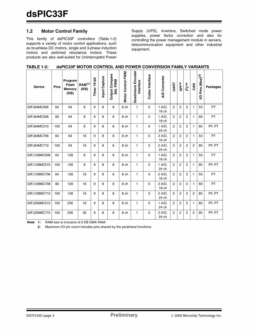
1.2 Motor Control Family
This family of dsPIC33F controllers (Table 1-2)supports a variety of motor control applications, suchas brushless DC motors, single and 3-phase inductionmotors and switched reluctance motors. Theseproducts are also well-suited for Uninterrupted Power
Supply (UPS), inverters, Switched mode powersupplies, power factor correction and also forcontrolling the power management module in servers,telecommunication equipment and other industrialequipment.
TABLE 1-2: dsPIC33F MOTOR CONTROL AND POWER CONVERSION FAMILY VARIANTS
Device Pins
Program Flash
Memory(KB)
RAM(1)
(KB)
Tim
er 1
6-b
it
Inp
ut
Cap
ture
Ou
tpu
t C
om
pare
Std
. PW
M
Mo
tor
Co
ntr
ol P
WM
Qu
adra
ture
En
cod
erIn
terf
ace
Co
dec
Inte
rfac
e
A/D
Co
nve
rter
UA
RT
SP
I™
I2 C™
CA
N
I/O P
ins
(Max
)(2)
Packages
33FJ64MC506 64 64 8 9 8 8 8 ch 1 0 1 A/D, 16 ch
2 2 2 1 53 PT
33FJ64MC508 80 64 8 9 8 8 8 ch 1 0 1 A/D, 18 ch
2 2 2 1 69 PT
33FJ64MC510 100 64 8 9 8 8 8 ch 1 0 1 A/D, 24 ch
2 2 2 1 85 PF, PT
33FJ64MC706 64 64 16 9 8 8 8 ch 1 0 2 A/D, 16 ch
2 2 2 1 53 PT
33FJ64MC710 100 64 16 9 8 8 8 ch 1 0 2 A/D, 24 ch
2 2 2 2 85 PF, PT
33FJ128MC506 64 128 8 9 8 8 8 ch 1 0 1 A/D, 16 ch
2 2 2 1 53 PT
33FJ128MC510 100 128 8 9 8 8 8 ch 1 0 1 A/D, 24 ch
2 2 2 1 85 PF, PT
33FJ128MC706 64 128 16 9 8 8 8 ch 1 0 2 A/D, 16 ch
2 2 2 1 53 PT
33FJ128MC708 80 128 16 9 8 8 8 ch 1 0 2 A/D, 18 ch
2 2 2 1 69 PT
33FJ128MC710 100 128 16 9 8 8 8 ch 1 0 2 A/D, 24 ch
2 2 2 2 85 PF, PT
33FJ256MC510 100 256 16 9 8 8 8 ch 1 0 1 A/D, 24 ch
2 2 2 1 85 PF, PT
33FJ256MC710 100 256 30 9 8 8 8 ch 1 0 2 A/D, 24 ch
2 2 2 2 85 PF, PT
Note 1: RAM size is inclusive of 2 KB DMA RAM.2: Maximum I/O pin count includes pins shared by the peripheral functions.
DS70155C-page 4 Preliminary © 2005 Microchip Technology Inc.
dsPIC33F
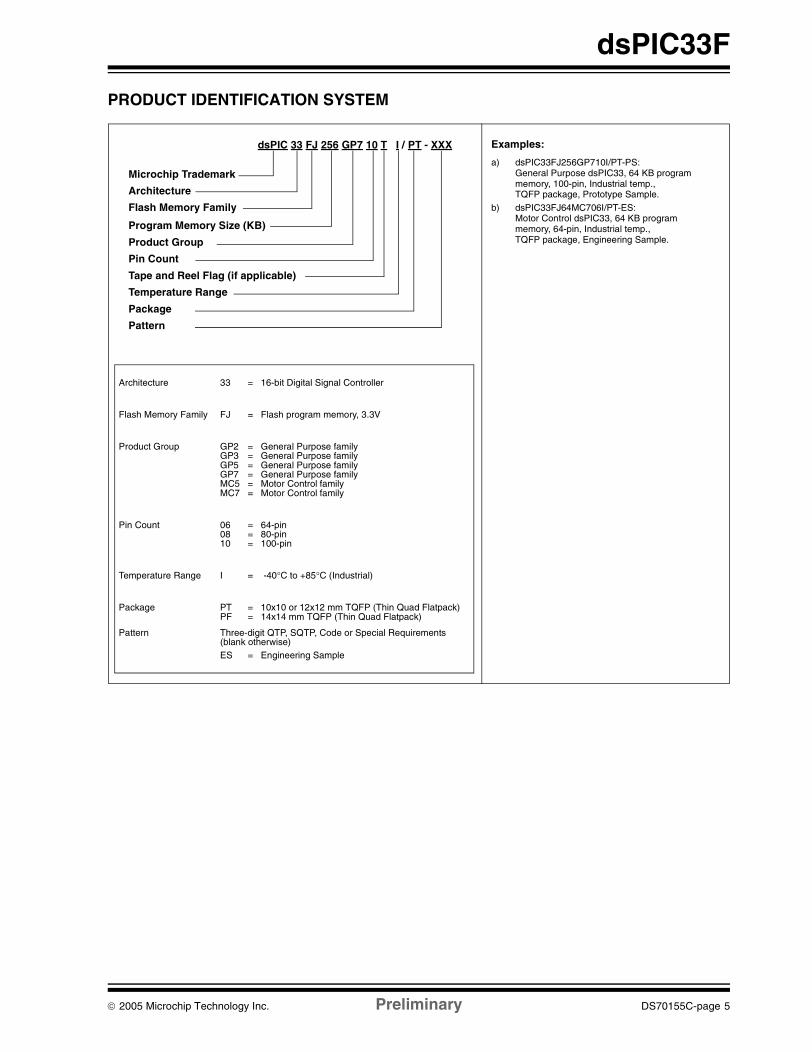
PRODUCT IDENTIFICATION SYSTEM
Architecture 33 = 16-bit Digital Signal Controller
Flash Memory Family FJ = Flash program memory, 3.3V
Product Group GP2 = General Purpose familyGP3 = General Purpose familyGP5 = General Purpose familyGP7 = General Purpose familyMC5 = Motor Control familyMC7 = Motor Control family
Pin Count 06 = 64-pin08 = 80-pin10 = 100-pin
Temperature Range I = -40°C to +85°C (Industrial)
Package PT = 10x10 or 12x12 mm TQFP (Thin Quad Flatpack)PF = 14x14 mm TQFP (Thin Quad Flatpack)
Pattern Three-digit QTP, SQTP, Code or Special Requirements (blank otherwise)ES = Engineering Sample
Examples:
a) dsPIC33FJ256GP710I/PT-PS:General Purpose dsPIC33, 64 KB program memory, 100-pin, Industrial temp.,TQFP package, Prototype Sample.
b) dsPIC33FJ64MC706I/PT-ES:Motor Control dsPIC33, 64 KB program memory, 64-pin, Industrial temp.,TQFP package, Engineering Sample.
Microchip Trademark
Architecture
Flash Memory Family
Program Memory Size (KB)
Product Group
Pin Count
Temperature Range
Package
Pattern
dsPIC 33 FJ 256 GP7 10 T I / PT - XXX
Tape and Reel Flag (if applicable)
© 2005 Microchip Technology Inc. Preliminary DS70155C-page 5

dsPIC33F
2.0 dsPIC33F DEVICE FAMILY OVERVIEW
The dsPIC33F device family employs a powerful 16-bitarchitecture that seamlessly integrates the controlfeatures of a Microcontroller (MCU) with thecomputational capabilities of a Digital Signal Processor(DSP). The resulting functionality is ideal forapplications that rely on high-speed, repetitivecomputations, as well as control.
The DSP engine, dual 40-bit accumulators, hardwaresupport for division operations, barrel shifter, 17 x 17multiplier, a large array of 16-bit working registers and
a wide variety of data addressing modes, togetherprovide the dsPIC33F Central Processing Unit (CPU)with extensive mathematical processing capability.Flexible and deterministic interrupt handling, coupledwith a powerful array of peripherals, renders thedsPIC33F devices suitable for control applications.Further, Direct Memory Access (DMA) enablesoverhead-free transfer of data between severalperipherals and a dedicated DMA RAM. Reliable, fieldprogrammable Flash program memory ensuresscalability of applications that use dsPIC33F devices.
Figure 2-1 shows a sample device block diagramtypical of the dsPIC33F product family.
FIGURE 2-1: dsPIC33F DEVICE BLOCK DIAGRAM
Barrel Shifter
ACCA<40>
ACCB<40>
DSP Engine
Divide Control
17 x 17 Multiplier
W RegisterArray
16 x 16
MemoryMapped
16-bit ALU
Program Flash Memory Data
Access
Y AGU
X AGU
Program Counter<23 bits>
InstructionPrefetch & Decode
X-Data Bus <16-bit>Y-Data Bus <16-bit>
Data SRAM up to
28 Kbytes
FlashProgramMemory
up to256 Kbytes
Peripherals
I/O Ports
24
23
Legend:
MCU/DSP X-Data Path
DSP Y-Data Path
Address Path
Status RegisterDual Port
RAM2 Kbytes
DMAController
DS70155C-page 6 Preliminary © 2005 Microchip Technology Inc.

dsPIC33F
3.0 CPU ARCHITECTURE
3.1 Overview
The dsPIC33F CPU module has a 16-bit (data)modified Harvard architecture with an enhancedinstruction set, including significant support for DSP.The CPU has a 24-bit instruction word with a variablelength opcode field. The Program Counter (PC) is23 bits wide and addresses up to 4M x 24 bits of userprogram memory space. The actual amount of programmemory implemented, as illustrated in Figure 3-1,varies from one device to another. A single-cycleinstruction prefetch mechanism is used to helpmaintain throughput and provides predictableexecution. All instructions execute in a single cycle,with the exception of instructions that change theprogram flow, the double word move (MOV.D)instruction and the table instructions. Overhead-freeprogram loop constructs are supported using the DOand REPEAT instructions, both of which areinterruptible at any point.
The dsPIC33F devices have sixteen 16-bit workingregisters in the programmer’s model. Each of theworking registers can serve as a data, address oraddress offset register. The 16th working register(W15) operates as a software Stack Pointer (SP) forinterrupts and calls.
The dsPIC33F instruction set has two classes ofinstructions: the MCU class of instructions and the DSPclass of instructions. These two instruction classes areseamlessly integrated into a single CPU. Theinstruction set includes many addressing modes and isdesigned for optimum C compiler efficiency.
3.1.1 DATA MEMORY OVERVIEW
The data space can be addressed as 32K words or64 Kbytes and is split into two blocks, referred to as Xand Y data memory. Each memory block has its ownindependent Address Generation Unit (AGU). TheMCU class of instructions operates solely through theX memory AGU, which accesses the entire memorymap as one linear data space. Certain DSP instructionsoperate through the X and Y AGUs to support dualoperand reads, which splits the data address spaceinto two parts. The X and Y data space boundary isdevice specific.
The upper 32 Kbytes of the data space memory mapcan optionally be mapped into program space at any16K program word boundary defined by the 8-bitProgram Space Visibility Page (PSVPAG) register. Theprogram-to-data space mapping feature lets anyinstruction access program space as if it were dataspace.
The data space includes 2 Kbytes of DMA RAM, whichis primarily used for DMA data transfers, but may beused as general purpose RAM.
FIGURE 3-1: PROGRAM SPACE MEMORY MAP
Reset – Target Address
Use
r M
emor
yS
pace
000000
0000FE
Reserved 000002
000100
Device Configuration
User FlashProgram Memory
02AC0002ABFE
Con
figur
atio
n M
emor
yS
pace
Osc. Fail Trap VectorAddress Error Trap Vector
Stack Error Trap VectorMath Error Trap Vector
DMA Error VectorReserved Vector
Interrupt Vector Table
(87296 x 24-bit)
800000
F80000Registers (12 x 8-bit) F80016
F80018
FFFFFE
F7FFFE
Reserved
000014 Vec
tor
Reset – GOTO Instruction
000004
Reserved
7FFFFE
Reserved
0002000001FE
000104Alternate Vector Table
Reserved
Tabl
esReserved Vector
Device ID (2 x 16-bit)
Reserved
FEFFFEFF0000FF0002FF0004
© 2005 Microchip Technology Inc. Preliminary DS70155C-page 7

dsPIC33F
3.1.2 ADDRESSING MODES OVERVIEW
Overhead-free circular buffers (modulo addressing) aresupported in both X and Y address spaces. Themodulo addressing removes the software boundarychecking overhead for DSP algorithms. Furthermore,the X AGU circular addressing can be used with any ofthe MCU class of instructions. The X AGU alsosupports bit-reversed addressing to greatly simplifyinput or output data reordering for radix-2 FFTalgorithms.
The CPU supports Inherent (no operand), Relative,Literal, Memory Direct, Register Direct and RegisterIndirect Addressing modes. Each instruction isassociated with a predefined addressing mode groupdepending upon its functional requirements. As manyas 6 addressing modes are supported for eachinstruction.
For most instructions, the dsPIC33F is capable ofexecuting a data (or program data) memory read, aworking register (data) read, a data memory write anda program (instruction) memory read per instructioncycle. As a result, three parameter instructions can besupported, allowing A + B = C operations to beexecuted in a single cycle.
3.1.3 DSP ENGINE OVERVIEW
The DSP engine features a high-speed, 17-bit by 17-bitmultiplier, a 40-bit ALU, two 40-bit saturatingaccumulators and a 40-bit bidirectional barrel shifter.The barrel shifter is capable of shifting a 40-bit value,up to 16 bits right or left, in a single cycle. The DSPinstructions operate seamlessly with all otherinstructions and have been designed for optimal real-time performance. The MAC instruction and otherassociated instructions can concurrently fetch two dataoperands from memory while multiplying two Wregisters and accumulating and optionally saturatingthe result in the same cycle. This instructionfunctionality requires that the RAM memory data spacebe split for these instructions and linear for all others.Data space partitioning is achieved in a transparentand flexible manner through dedicating certain workingregisters to each address space.
3.1.4 SPECIAL MCU FEATURES
The dsPIC33F features a 17-bit by 17-bit, single-cyclemultiplier that is shared by both the MCU ALU and DSPengine. The multiplier can perform signed, unsignedand mixed-sign multiplication. Using a 17-bit by 17-bitmultiplier for 16-bit by 16-bit multiplication not onlyallows you to perform mixed-sign multiplication, it alsoachieves accurate results for special operations suchas (-1.0) x (-1.0).
The dsPIC33F supports 16/16 and 32/16 divideoperations, both fractional and integer. All divideinstructions are iterative operations. They must beexecuted within a REPEAT loop, resulting in a totalexecution time of 19 instruction cycles. The divideoperation can be interrupted during any of those 19cycles without loss of data.
A 40-bit barrel shifter is used to perform up to a 16-bitleft or right shift in a single cycle. The barrel shifter canbe used by both MCU and DSP instructions.
3.1.5 INTERRUPT OVERVIEW
The dsPIC33F has a vectored exception scheme withup to 5 sources of non-maskable traps and 67 interruptsources. Each interrupt source can be assigned to oneof seven priority levels.
3.1.6 FEATURES TO ENHANCE COMPILER EFFICIENCY
In addition to extensive DSP capability, the CPUarchitecture possesses several features that lead to amore efficient (code size and speed) C compiler.
1. For most instructions, three-parameter instruc-tions can be supported, allowing A + B = Coperations to be executed in a single cycle.
2. Instruction addressing modes are extremelyflexible to meet compiler needs.
3. The working register array consists of 16 x 16-bitregisters, each of which can act as data,address or offset registers. One working register(W15) operates as the software Stack Pointerfor interrupts and calls.
4. Linear indirect access of all data space ispossible, plus the memory direct address rangeis up to 8 Kbytes. This capability, together withthe addition of 16-bit direct address MOV-basedinstructions, has provided a contiguous linearaddressing space.
5. Linear indirect access of 32K word (64 Kbyte)pages within program space is possible, usingany working register via new table read andwrite instructions.
6. Part of data space can be mapped into programspace, allowing constant data to be accessed asif it were in data space.
DS70155C-page 8 Preliminary © 2005 Microchip Technology Inc.

dsPIC33F
3.2 Programmer’s Model
The programmer’s model, shown in Figure 3-2,consists of 16 x 16-bit working registers (W0 throughW15), 2 x 40-bit accumulators (ACCA and ACCB),Status Register (SR), Data Table Page register(TBLPAG), Program Space Visibility Page register(PSVPAG), DO and REPEAT registers (DOSTART,DOEND, DCOUNT and RCOUNT) and ProgramCounter (PC). The working registers can act as data,address or offset registers. All registers are memorymapped. W0 is the W register for all instructions thatperform file register addressing.
Some of these registers have a shadow registerassociated with them (see the legend in Figure 3-2).The shadow register is used as a temporary holdingregister and can transfer its contents to or from its hostregister upon some event occurring in a single cycle.None of the shadow registers are accessible directly.
When a byte operation is performed on a workingregister, only the Least Significant Byte of the targetregister is affected. However, a benefit of memorymapped working registers is that both the Least andMost Significant Bytes can be manipulated throughbyte-wide data memory space accesses.
W15 is the dedicated software Stack Pointer (SP). It isautomatically modified by exception processing andsubroutine calls and returns. However, W15 can bereferenced by any instruction in the same manner as allother W registers. This simplifies the reading, writingand manipulation of the Stack Pointer (e.g., creatingstack frames).
W14 has been dedicated as a Stack Frame Pointer, asdefined by the LNK and ULNK instructions. However,W14 can be referenced by any instruction in the samemanner as all other W registers.
The Stack Pointer always points to the first availablefree word and grows from lower addresses towardshigher addresses. It pre-decrements for stack pops(reads) and post-increments for stack pushes (writes).
© 2005 Microchip Technology Inc. Preliminary DS70155C-page 9

dsPIC33F
FIGURE 3-2: PROGRAMMER’S MODEL
TABPAG
22 0
7 0
015
Program Counter
Data Table Page Address
Status Register
Working Registers
MAC OperandRegisters
W1
W2
W3
W4
W5
W6
W7
W8
W9
W10
W11
W12/MAC Offset
W13/MAC Write Back
W14/Frame Pointer
W15*/Stack Pointer
MAC AddressRegisters
39 031
DSPAccumulators
ACCA
ACCB
PSVPAG7 0
Program Space Visibility Page Address
Z OA OB SA SB
RCOUNT15 0
REPEAT Loop Counter
DCOUNT15 0
DO Loop Counter
DOSTART
22 0DO Loop Start Address
IPL2 IPL1
SPLIM* Stack Pointer Limit Register
15
SRL
PUSH.S Shadow
DO Shadow
OAB SAB
15 0 Core Configuration Register
Legend:
CORCON
DA DC RA N
TBLPAG
PSVPAG
IPL0 OV
W0/WREG
SRH
DO Loop End AddressDOEND
22
C
0
DIV and MULResult Registers
*W15 and SPLIM not shadowed
DS70155C-page 10 Preliminary © 2005 Microchip Technology Inc.
dsPIC33F
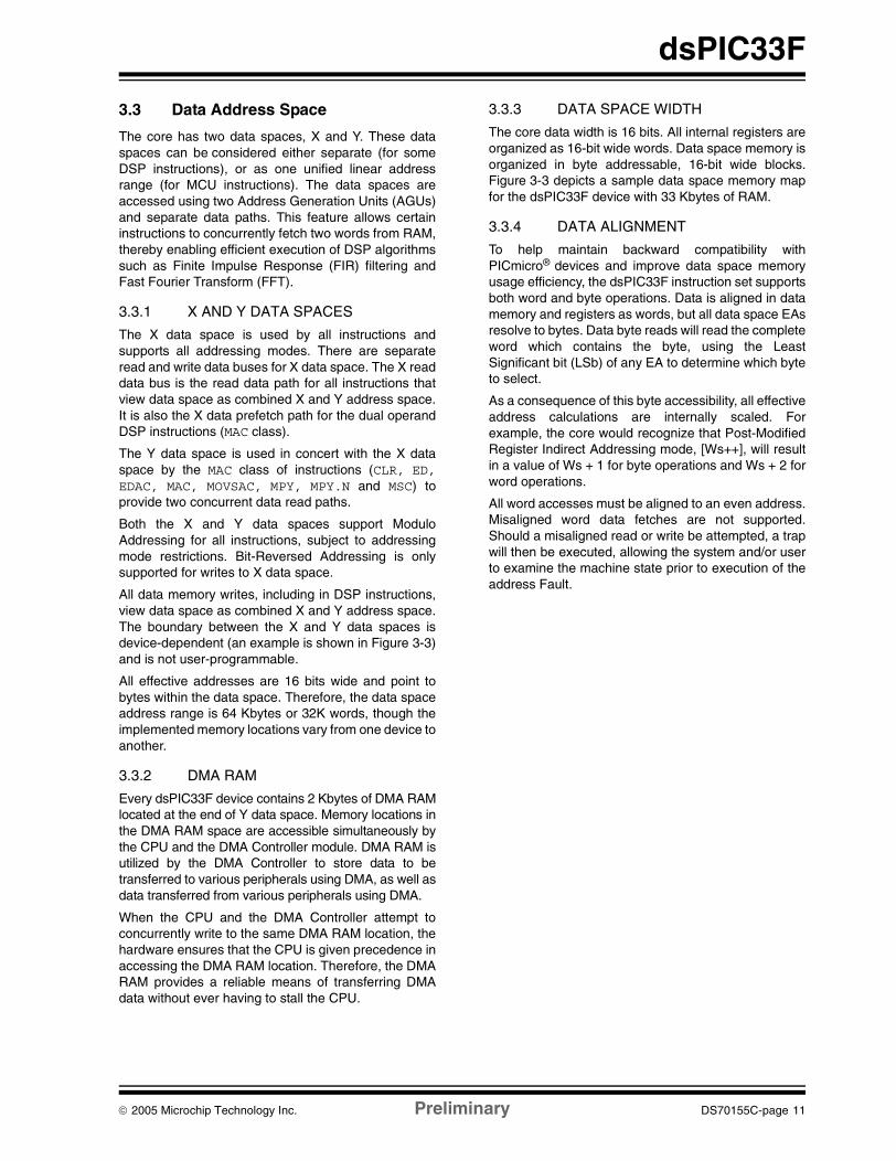
3.3 Data Address Space
The core has two data spaces, X and Y. These dataspaces can be considered either separate (for someDSP instructions), or as one unified linear addressrange (for MCU instructions). The data spaces areaccessed using two Address Generation Units (AGUs)and separate data paths. This feature allows certaininstructions to concurrently fetch two words from RAM,thereby enabling efficient execution of DSP algorithmssuch as Finite Impulse Response (FIR) filtering andFast Fourier Transform (FFT).
3.3.1 X AND Y DATA SPACES
The X data space is used by all instructions andsupports all addressing modes. There are separateread and write data buses for X data space. The X readdata bus is the read data path for all instructions thatview data space as combined X and Y address space.It is also the X data prefetch path for the dual operandDSP instructions (MAC class).
The Y data space is used in concert with the X dataspace by the MAC class of instructions (CLR, ED,EDAC, MAC, MOVSAC, MPY, MPY.N and MSC) toprovide two concurrent data read paths.
Both the X and Y data spaces support ModuloAddressing for all instructions, subject to addressingmode restrictions. Bit-Reversed Addressing is onlysupported for writes to X data space.
All data memory writes, including in DSP instructions,view data space as combined X and Y address space.The boundary between the X and Y data spaces isdevice-dependent (an example is shown in Figure 3-3)and is not user-programmable.
All effective addresses are 16 bits wide and point tobytes within the data space. Therefore, the data spaceaddress range is 64 Kbytes or 32K words, though theimplemented memory locations vary from one device toanother.
3.3.2 DMA RAM
Every dsPIC33F device contains 2 Kbytes of DMA RAMlocated at the end of Y data space. Memory locations inthe DMA RAM space are accessible simultaneously bythe CPU and the DMA Controller module. DMA RAM isutilized by the DMA Controller to store data to betransferred to various peripherals using DMA, as well asdata transferred from various peripherals using DMA.
When the CPU and the DMA Controller attempt toconcurrently write to the same DMA RAM location, thehardware ensures that the CPU is given precedence inaccessing the DMA RAM location. Therefore, the DMARAM provides a reliable means of transferring DMAdata without ever having to stall the CPU.
3.3.3 DATA SPACE WIDTH
The core data width is 16 bits. All internal registers areorganized as 16-bit wide words. Data space memory isorganized in byte addressable, 16-bit wide blocks.Figure 3-3 depicts a sample data space memory mapfor the dsPIC33F device with 33 Kbytes of RAM.
3.3.4 DATA ALIGNMENT
To help maintain backward compatibility withPICmicro® devices and improve data space memoryusage efficiency, the dsPIC33F instruction set supportsboth word and byte operations. Data is aligned in datamemory and registers as words, but all data space EAsresolve to bytes. Data byte reads will read the completeword which contains the byte, using the LeastSignificant bit (LSb) of any EA to determine which byteto select.
As a consequence of this byte accessibility, all effectiveaddress calculations are internally scaled. Forexample, the core would recognize that Post-ModifiedRegister Indirect Addressing mode, [Ws++], will resultin a value of Ws + 1 for byte operations and Ws + 2 forword operations.
All word accesses must be aligned to an even address.Misaligned word data fetches are not supported.Should a misaligned read or write be attempted, a trapwill then be executed, allowing the system and/or userto examine the machine state prior to execution of theaddress Fault.
© 2005 Microchip Technology Inc. Preliminary DS70155C-page 11

dsPIC33F
FIGURE 3-3: SAMPLE DATA SPACE MEMORY MAP
0x0000
0x07FE
SFR Space
0xFFFE
X Data RAM (X)
Least Significant ByteAddress16 Bits
LSBMSB
Most Significant ByteAddress
0x0001
0x07FF
0xFFFF
X Data
0x7800
OptionallyMappedinto ProgramMemory
Unimplemented (X)
0x0801 0x0800
2-KbyteSFR Space
0x40000x3FFE
DMA RAM
0x40010x3FFF
0x77FE
8-Kbyte
Data Space
0x77FF0x7801
0x7FFF 0x7FFE
Note: This data memory map is for the largest memory dsPIC33F device. Data memory maps for otherdevices may vary.
Y Data RAM (Y)
0x8001 0x8000
DS70155C-page 12 Preliminary © 2005 Microchip Technology Inc.

dsPIC33F
3.4 DSP Engine
The DSP engine consists of a high-speed, single-cycle, 17-bit x 17-bit multiplier, a barrel shifter and a40-bit adder/subtractor with two target accumulators,round and saturation logic, all of which enable efficientexecution of computationally intensive DSPalgorithms. The 17-bit x 17-bit multiplier is also utilizedfor MCU-based multiply instructions.
The DSP engine also has the capability to performinherent accumulator-to-accumulator operations, whichrequire no additional data. These instructions are ADD,SUB and NEG. This feature greatly simplifies basicarithmetic operations on 32-bit or 40-bit data.
A block diagram of the DSP engine is shown inFigure 3-4.
3.4.1 17 x 17-BIT MULTIPLIER
The 17 x 17-bit multiplier is capable of signed orunsigned operation. It can suitably scale its output tosupport either 1.31 fractional (Q31) or 32-bit integerresults, thereby diminishing the need to manuallypost-process multiplication results for fractional data.
3.4.2 40-BIT ACCUMULATORS
The data accumulators have a 40-bit adder/subtractorwith automatic sign extension logic. It can select one oftwo accumulators (A or B) as its pre-accumulationsource and post-accumulation destination. For the ADDand LAC instructions, the data to be accumulated orloaded can be optionally scaled via the barrel shifterprior to accumulation.
The adder/subtractor generates overflow status bits,SA/SB and OA/OB, which are latched and reflected inthe Status register and can also optionally generate anarithmetic error trap:
• Overflow from bit 39. This is a catastrophic overflow in which the sign of the accumulator is destroyed.
• Overflow into guard bits 32 through 39. This is a recoverable overflow. This bit (OA/OB) is set whenever all the guard bits are not identical to each other.
3.4.3 SATURATION AND OVERFLOW
The adder has an additional saturation block thatcontrols accumulator data saturation, if selected. Ituses the result of the adder, the overflow status bitsdescribed above and the user-configured control bits todetermine when to saturate and to what value tosaturate (a 40-bit or a 32-bit value).
In addition to adder/subtractor saturation, writes to dataspace can also be saturated, but without affecting thecontents of the source accumulator.
The rounding logic performs a conventional (biased) orconvergent (unbiased) data rounding function duringan accumulator write (store). The Round mode is user-selectable. Rounding generates a 16-bit, 1.15 datavalue, which is passed to the data space writesaturation logic. Data space write saturation ensuresthat the data in the accumulator is written backaccurately even when rounding is performed. Ifrounding is not indicated by the instruction, a truncated1.15 data value is stored and the least significant wordis simply discarded.
© 2005 Microchip Technology Inc. Preliminary DS70155C-page 13

dsPIC33F
FIGURE 3-4: DSP ENGINE BLOCK DIAGRAM
Zero Backfill
Sign-Extend
BarrelShifter
40-bit Accumulator A
40-bit Accumulator BRound
Logic
X D
ata
Bus
Multiplier/Scaler
To/From W Array
Adder
Saturate
Operand Latches
Enable
17-bit
Negate
32
3233
16
16 16
16
4040
40 40
Saturate
Y D
ata
Bus
40
16
40
DS70155C-page 14 Preliminary © 2005 Microchip Technology Inc.

dsPIC33F
4.0 DIRECT MEMORY ACCESS
Direct Memory Access (DMA) is a very efficientmechanism of copying data between peripheral SFRs(e.g., UART Receive register, Input Capture 1 buffer)and buffers or variables stored in RAM with minimalCPU intervention. The DMA Controller canautomatically copy entire blocks of data, without theuser software having to read or write peripheral SpecialFunction Registers (SFRs) every time a peripheralinterrupt occurs. To exploit the DMA capability, thecorresponding user buffers or variables must belocated in DMA RAM space.
The DMA Controller features eight identical datatransfer channels, each with its own set of control andstatus registers. The UART, SPI, DCI, Input Capture,Output Compare, ECAN™ and A/D modules can utilizeDMA. Each DMA channel can be configured to copydata either from buffers stored in DMA RAM toperipheral SFRs or from peripheral SFRs to buffers inDMA RAM.
Each channel supports the following features:
• Word or byte-sized data transfers• Transfers from peripheral to DMA RAM or DMA
RAM to peripheral
• Indirect addressing of DMA RAM locations with or without automatic post-increment
• Peripheral Indirect Addressing – In some peripherals, the DMA RAM read/write addresses may be partially derived from the peripheral
• One-Shot Block Transfers – Terminating DMA transfer after one block transfer
• Continuous Block Transfers – Reloading DMA RAM buffer start address after every block transfer is complete
• Ping-Pong Mode – Switching between two DMA RAM start addresses between successive block transfers, thereby filling two buffers alternately
• Automatic or manual initiation of block transfers• Each channel can select from 32 possible
sources of data sources or destinations
For each DMA channel, a DMA interrupt request isgenerated when a block transfer is complete.Alternatively, an interrupt can be generated when half ofthe block has been filled. Additionally, a DMA error trapis generated in either of the following Fault conditions:
• DMA RAM data write collision between the CPU and a peripheral
• Peripheral SFR data write collision between the CPU and the DMA Controller
FIGURE 4-1: TOP LEVEL SYSTEM ARCHITECTURE USING A DEDICATED TRANSACTION BUS
CPU
SRAM DMA RAM
CPU Peripheral DS Bus
Peripheral 3
DMA
Peripheral
Non-DMA
SRAM X-Bus
PORT 2PORT 1
Peripheral 1
DMAReady
Peripheral 2
DMAReadyReady
Ready
DMA DS Bus
CPU DMA
CPU DMA CPU DMA
Peripheral Indirect Address
Note: CPU and DMA address buses are not shown for clarity.
DM
AC
ontr
ol
DMA Controller
ChannelsDMA
© 2005 Microchip Technology Inc. Preliminary DS70155C-page 15

dsPIC33F
5.0 EXCEPTION PROCESSING
The dsPIC33F has four processor exceptions (traps)and up to 67 sources of interrupts, which must bearbitrated based on a priority scheme.
The processor core is responsible for reading theInterrupt Vector Table (IVT) and transferring theaddress contained in the interrupt vector to theprogram counter.
The Interrupt Vector Table (IVT) and Alternate InterruptVector Table (AIVT) are placed near the beginning ofprogram memory (0x000004) for ease of debugging.
The interrupt controller hardware pre-processes theinterrupts before they are presented to the CPU.The interrupts and traps are enabled, prioritized andcontrolled using centralized Special Function Registers.
Each individual interrupt source has its own vectoraddress and can be individually enabled and prioritizedin user software. Each interrupt source also has its ownstatus flag. This independent control and monitoring ofthe interrupt eliminates the need to poll various statusflags to determine the interrupt source
Table 5-1 contains information about the interruptvector.
Certain interrupts have specialized control bits forfeatures like edge or level triggered interrupts, interrupt-on-change, etc. Control of these features remains withinthe peripheral module, which generates the interrupt.
The special DISI instruction can be used to disablethe processing of interrupts of priorities 6 and lower fora certain number of instruction cycles, during whichthe DISI bit remains set.
TABLE 5-1: INTERRUPT VECTORS
Vector Number
IVT Address AIVT Address Interrupt Source
8 0x000014 0x000114 INT0 – External Interrupt 0
9 0x000016 0x000116 IC1 – Input Compare 1
10 0x000018 0x000118 OC1 – Output Compare 1
11 0x00001A 0x00011A T1 – Timer1
12 0x00001C 0x00011C DMA0 – DMA Channel 0
13 0x00001E 0x00011E IC2 – Input Capture 2
14 0x000020 0x000120 OC2 – Output Compare 2
15 0x000022 0x000122 T2 – Timer2
16 0x000024 0x000124 T3 – Timer3
17 0x000026 0x000126 SPI1E – SPI1 Error
18 0x000028 0x000128 SPI1D – SPI1 Transfer Done
19 0x00002A 0x00012A U1RX – UART1 Receiver
20 0x00002C 0x00012C U1TX – UART1 Transmitter
21 0x00002E 0x00012E ADC1 – A/D Converter 1
22 0x000030 0x000130 DMA1 – DMA Channel 1
23 0x000032 0x000132 Reserved
24 0x000034 0x000134 I2C1D – I2C1 Transfer Done
25 0x000036 0x000136 I2C1E – I2C1 Bus Collision Error
26 0x000038 0x000138 Reserved
27 0x00003A 0x00013A Change Notification Interrupt
28 0x00003C 0x00013C INT1 – External Interrupt 1
29 0x00003E 0x00013E ADC2 – A/D Converter 2
30 0x000040 0x000140 IC7 – Input Capture 7
31 0x000042 0x000142 IC8 – Input Capture 8
32 0x000044 0x000144 DMA2 – DMA Channel 2
33 0x000046 0x000146 OC3 – Output Compare 3
34 0x000048 0x000148 OC4 – Output Compare 4
35 0x00004A 0x00014A T4 – Timer4
36 0x00004C 0x00014C T5 – Timer5
37 0x00004E 0x00014E INT2 – External Interrupt 2
38 0x000050 0x000150 U2RX – UART2 Receiver
39 0x000052 0x000152 U2TX – UART2 Transmitter
DS70155C-page 16 Preliminary © 2005 Microchip Technology Inc.

dsPIC33F
40 0x000054 0x000154 SPI2E – SPI2 Error
41 0x000056 0x000156 SPI1D – SPI1 Transfer Done
42 0x000058 0x000158 C1RX – ECAN1 Receive Data Ready
43 0x00005A 0x00015A C1 – CAN1 Event
44 0x00005C 0x00015C DMA3 – DMA Channel 3
45 0x00005E 0x00015E IC3 – Input Capture 3
46 0x000060 0x000160 IC4 – Input Capture 4
47 0x000062 0x000162 IC5 – Input Capture 5
48 0x000064 0x000164 IC6 – Input Capture 6
49 0x000066 0x000166 OC5 – Output Compare 5
50 0x000068 0x000168 OC6 – Output Compare 6
51 0x00006A 0x00016A OC7 – Output Compare 7
52 0x00006C 0x00016C OC8 – Output Compare 8
53 0x00006E 0x00016E Reserved
54 0x000070 0x000170 DMA4 – DMA Channel 4
55 0x000072 0x000172 T6 – Timer6
56 0x000074 0x000174 T7 – Timer7
57 0x000076 0x000176 I2C2D – I2C2 Transfer Done
58 0x000078 0x000178 I2C2E – I2C2 Bus Collision Error
59 0x00007A 0x00017A T8 – Timer8
60 0x00007C 0x00017C T9 – Timer9
61 0x00007E 0x00017E INT3 – External Interrupt 3
62 0x000080 0x000180 INT4 – External Interrupt 4
63 0x000082 0x000182 C2RX – ECAN2 Receive Data Ready
64 0x000084 0x000184 C2 – CAN2 Event
65 0x000086 0x000186 PWM – PWM Period Match
66 0x000088 0x000188 QEI – Position Counter Compare
67 0x00008A 0x00018A DCIE – DCI Error
68 0x00008C 0x00018C DCID – DCI Transfer Done
69 0x00008E 0x00018E DMA5 – DMA Channel 5
70 0x000090 0x000190 RTC – Real-Time Clock
71 0x000092 0x000192 FLTA – MCPWM Fault A
72 0x000094 0x000194 FLTB – MCPWM Fault B
73 0x000096 0x000196 U1E – UART1 Error
74 0x000098 0x000198 U2E – UART2 Error
75 0x00009A 0x00019A Reserved
76 0x00009C 0x00019C DMA6 – DMA Channel 6
77 0x00009E 0x00019E DMA7 – DMA Channel 7
78 0x0000A0 0x0001A0 C1TX – ECAN1 Transmit Data Request
Reserved (for devices marked “PS”)
79 0x0000A2 0x0001A2 C2TX – ECAN2 Transmit Data Request
Reserved (for devices marked “PS”)
80-125 0x0000A4-0x0000FE
0x0001A4-0x0001FE
Reserved
TABLE 5-1: INTERRUPT VECTORS (CONTINUED)
Vector Number
IVT Address AIVT Address Interrupt Source
© 2005 Microchip Technology Inc. Preliminary DS70155C-page 17

dsPIC33F
5.1 Interrupt Priority
Each interrupt source can be user-assigned to one of8 priority levels, 0 through 7. Levels 7 and 1 representthe highest and lowest maskable priorities,respectively. A priority level of 0 disables the interrupt.
Since more than one interrupt request source may beassigned to a user-specified priority level, a means isprovided to assign priority within a given level. Thismethod is called “Natural Order Priority”.
The Natural Order Priority of an interrupt is numericallyidentical to its vector number. The Natural OrderPriority scheme has 0 as the highest priority and 74 asthe lowest priority.
The ability for the user to assign every interrupt to oneof eight priority levels implies that the user can assigna very high overall priority level to an interrupt with alow Natural Order Priority, thereby providing muchflexibility in designing applications that use a largenumber of peripherals.
5.2 Interrupt Nesting
Interrupts, by default, are nestable. Any ISR that is inprogress may be interrupted by another source ofinterrupt with a higher user-assigned priority level.Interrupt nesting may be optionally disabled bysetting the NSTDIS control bit (INTCON1<15>).When the NSTDIS control bit is set, all interrupts inprogress will force the CPU priority to level 7 bysetting IPL<2:0> = 111. This action will effectivelymask all other sources of interrupt until a RETFIEinstruction is executed. When interrupt nesting isdisabled, the user-assigned interrupt priority levelswill have no effect, except to resolve conflictsbetween simultaneous pending interrupts.
The IPL<2:0> bits become read-only when interruptnesting is disabled. This prevents the user softwarefrom setting IPL<2:0> to a lower value, which wouldeffectively re-enable interrupt nesting.
5.3 Traps
Traps can be considered as non-maskable, nestableinterrupts that adhere to a fixed priority structure.Traps are intended to provide the user a means tocorrect erroneous operation during debug and whenoperating within the application. If the user does notintend to take corrective action in the event of a traperror condition, these vectors must be loaded with theaddress of a software routine that will reset the device.Otherwise, the trap vector is programmed with theaddress of a service routine that will correct the trapcondition.
The dsPIC33F has four implemented sources ofnon-maskable traps:
• Oscillator Failure Trap• Address Error Trap• Stack Error Trap
• Math Error Trap• DMA Trap
Many of these trap conditions can only be detectedwhen they happen. Consequently, the instruction thatcaused the trap is allowed to complete beforeexception processing begins. Therefore, the user mayhave to correct the action of the instruction thatcaused the trap.
Each trap source has a fixed priority as defined by itsposition in the IVT. An oscillator failure trap has thehighest priority, while an arithmetic error trap has thelowest priority.
Table 5-2 contains information about the trap vector.
5.4 Generating a Software Interrupt
Any available interrupt can be manually generated byuser software (even if the corresponding peripheral isdisabled), simply by enabling the interrupt and thensetting the interrupt flag bit when required.
TABLE 5-2: TRAP VECTORS
Vector Number IVT Address AIVT Address Trap Source
0 0x000004 0x000084 Reserved
1 0x000006 0x000086 Oscillator Failure
2 0x000008 0x000088 Address Error
3 0x00000A 0x00008A Stack Error
4 0x00000C 0x00008C Math Error
5 0x00000E 0x00008E DMA Error Trap
6 0x000010 0x000090 Reserved
7 0x000012 0x000092 Reserved
DS70155C-page 18 Preliminary © 2005 Microchip Technology Inc.

dsPIC33F
6.0 SYSTEM INTEGRATION
System management services provided by thedsPIC33F device family include:
• Control of clock options and oscillators
• Power-on Reset• Oscillator Start-up Timer/Stabilizer• Watchdog Timer with RC oscillator
• Fail-Safe Clock Monitor• Reset by multiple sources
6.1 Clock Options and Oscillators
There are 7 clock options provided by the dsPIC33F:
• FRC Oscillator• FRC Oscillator with PLL
• Primary (XT, HS or EC) Oscillator• Primary Oscillator with PLL• Secondary (LP) Oscillator
• LPRC Oscillator
The FRC (Fast RC) internal oscillator runs at a nominalfrequency of 7.37 MHz. The user software can tune theFRC frequency. User software can specify a factor bywhich this clock frequency is scaled.
The primary oscillator can use one of the following asits clock source:
1. XT (Crystal): Crystals and ceramic resonators inthe range of 3 MHz to 10 MHz. The crystal isconnected to the OSC1 and OSC2 pins.
2. HS (High-Speed Crystal): Crystals in the rangeof 10 MHz to 40 MHz. The crystal is connectedto the OSC1 and OSC2 pins.
3. EC (External Clock): External clock signal in therange of 0.8 MHz to 64 MHz. The external clocksignal is directly applied to the OSC1 pin.
The secondary (LP) oscillator is designed for low powerand uses a 32 kHz crystal or ceramic resonator. The LPoscillator uses the SOSCI and SOSCO pins.
The LPRC (Low-Power RC) internal oscIllator runs at anominal frequency of 32.768 kHz. Another scaledreference clock is used by the Watchdog Timer (WDT)and Fail-Safe Clock Monitor (FSCM).
The clock signals generated by the FRC and primaryoscillators can be optionally applied to an on-chipPhase Locked Loop (PLL) to provide a wide range ofoutput frequencies for device operation. The input tothe PLL can be in the range of 1.6 MHz to 16 MHz, andthe PLL Phase Detector Input Divider, PLL MultiplierRatio and PLL Voltage Controlled Oscillator (VCO) canbe individually configured by user software to generateoutput frequencies in the range of 25 MHz to 160 MHz.
The output of the oscillator (or the output of the PLL ifa PLL mode has been selected) is divided by 4 togenerate the device instruction clock (FCY). FCY
defines the operating speed of the device, and speedsup to 40 MHz are supported by the dsPIC33Farchitecture.
The dsPIC33F oscillator system provides:
• Various external and internal oscillator options as clock sources
• An on-chip PLL to scale the internal operating frequency to the required system clock frequency
• The internal FRC oscillator can also be used with the PLL, thereby allowing full-speed operation without any external clock generation hardware
• Clock switching between various clock sources
• Programmable clock postscaler for system power savings
• A Fail-Safe Clock Monitor (FSCM) that detects clock failure and takes fail-safe measures
• A Clock Control register (OSCCON)• Nonvolatile configuration bits for main oscillator
selection.
A simplified block diagram of the oscillator system isshown in Figure 6-1.
© 2005 Microchip Technology Inc. Preliminary DS70155C-page 19
dsPIC33F
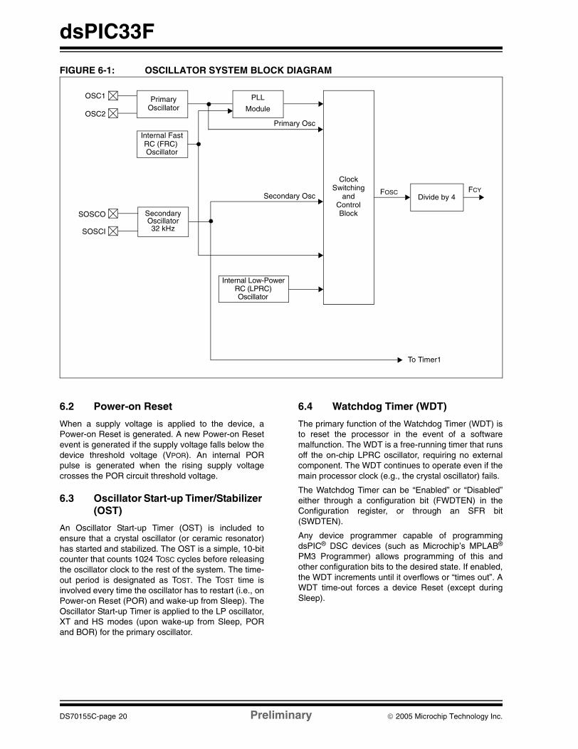
FIGURE 6-1: OSCILLATOR SYSTEM BLOCK DIAGRAM
6.2 Power-on Reset
When a supply voltage is applied to the device, aPower-on Reset is generated. A new Power-on Resetevent is generated if the supply voltage falls below thedevice threshold voltage (VPOR). An internal PORpulse is generated when the rising supply voltagecrosses the POR circuit threshold voltage.
6.3 Oscillator Start-up Timer/Stabilizer (OST)
An Oscillator Start-up Timer (OST) is included toensure that a crystal oscillator (or ceramic resonator)has started and stabilized. The OST is a simple, 10-bitcounter that counts 1024 TOSC cycles before releasingthe oscillator clock to the rest of the system. The time-out period is designated as TOST. The TOST time isinvolved every time the oscillator has to restart (i.e., onPower-on Reset (POR) and wake-up from Sleep). TheOscillator Start-up Timer is applied to the LP oscillator,XT and HS modes (upon wake-up from Sleep, PORand BOR) for the primary oscillator.
6.4 Watchdog Timer (WDT)
The primary function of the Watchdog Timer (WDT) isto reset the processor in the event of a softwaremalfunction. The WDT is a free-running timer that runsoff the on-chip LPRC oscillator, requiring no externalcomponent. The WDT continues to operate even if themain processor clock (e.g., the crystal oscillator) fails.
The Watchdog Timer can be “Enabled” or “Disabled”either through a configuration bit (FWDTEN) in theConfiguration register, or through an SFR bit(SWDTEN).
Any device programmer capable of programmingdsPIC® DSC devices (such as Microchip’s MPLAB®
PM3 Programmer) allows programming of this andother configuration bits to the desired state. If enabled,the WDT increments until it overflows or “times out”. AWDT time-out forces a device Reset (except duringSleep).
OSC1
Secondary Oscillator32 kHz
PLL
Module
Clock Switching
and Control Block
OSC2
SOSCO
SOSCI
FOSC
Primary Osc
Secondary Osc
To Timer1
Internal FastRC (FRC) Oscillator
Internal Low-PowerRC (LPRC)Oscillator
PrimaryOscillator
FCYDivide by 4
DS70155C-page 20 Preliminary © 2005 Microchip Technology Inc.

dsPIC33F
6.5 Fail-Safe Clock Monitor (FSCM)
The Fail-Safe Clock Monitor (FSCM) allows the deviceto continue to operate even in the event of an oscillatorfailure. The FSCM function is enabled by programming.If the FSCM function is enabled, the LPRC internaloscillator runs at all times (except during Sleep mode)and is not subject to control by the Watchdog Timer.
In the event of an oscillator failure, the FSCMgenerates a clock failure trap event and switches thesystem clock over to the FRC oscillator. The applicationprogram then can either attempt to restart the oscillator,or execute a controlled shutdown. The trap can betreated as a warm Reset by simply loading the Resetaddress into the oscillator fail trap vector.
6.6 Reset System
The Reset system combines all Reset sources andcontrols the device Master Reset signal.
Device Reset sources include:
• POR: Power-on Reset• BOR: Brown-out Reset
• SWR: RESET Instruction• EXTR: MCLR Reset• WDTR: Watchdog Timer Time-out Reset
• TRAPR: Trap Conflict • IOPUWR: Attempted execution of an Illegal
Opcode, or Indirect Addressing, using an Uninitialized W register
© 2005 Microchip Technology Inc. Preliminary DS70155C-page 21

dsPIC33F
DS
7.0 DEVICE POWER MANAGEMENT
Power management services provided by thedsPIC33F devices include:
• Real-Time Clock Source Switching
• Power-Saving Modes
7.1 Real-Time Clock Source Switching
Configuration bits determine the clock source uponPower-on Reset (POR) and Brown-out Reset (BOR).Thereafter, the clock source can be changed betweenpermissible clock sources. The OSCCON registercontrols the clock switching and reflects system clockrelated status bits. To reduce power consumption, theuser can switch to a slower clock source.
7.2 Power-Saving Modes
The dsPIC33F devices have two reduced powermodes that can be entered through execution of thePWRSAV instruction.
• Sleep Mode: The CPU, system clock source and any peripherals that operate on the system clock source are disabled. This is the lowest power mode of the device.
• Idle Mode: The CPU is disabled but the system clock source continues to operate. Peripherals continue to operate but can optionally be disabled.
• Doze Mode: The CPU clock is temporarily slowed down relative to the peripheral clock by a user-selectable factor.
These modes provide an effective way to reduce powerconsumption during periods when the CPU is not in use.
7.2.1 SLEEP MODE
When the device enters Sleep mode:
• System clock source is shut down. If an on-chip oscillator is used, it is turned off.
• Device current consumption is at minimum provided that no I/O pin is sourcing current.
• Fail-Safe Clock Monitor (FSCM) does not operate during Sleep mode because the system clock source is disabled.
• LPRC clock continues to run in Sleep mode if the WDT is enabled.
• BOR circuit, if enabled, remains operative during Sleep mode
• WDT, if enabled, is automatically cleared prior to entering Sleep mode.
• Some peripherals may continue to operate in Sleep mode. These peripherals include I/O pins that detect a change in the input signal, or peripherals that use an external clock input. Any peripheral that is operating on the system clock source is disabled in Sleep mode.
The processor exits (wakes up) from Sleep on one ofthese events:
• Any interrupt source that is individually enabled• Any form of device Reset• A WDT time-out
7.2.2 IDLE MODE
When the device enters Idle mode:
• CPU stops executing instructions
• WDT is automatically cleared• System clock source remains active• Peripheral modules, by default, continue to
operate normally from the system clock source• Peripherals, optionally, can be shut down in Idle
mode using their ‘stop-in-idle’ control bit.• If the WDT or FSCM is enabled, the LPRC also
remains active
The processor wakes from Idle mode on these events:
• Any interrupt that is individually enabled• Any source of device Reset
• A WDT time-out
Upon wake-up from Idle, the clock is re-applied to theCPU and instruction execution begins immediatelystarting with the instruction following the PWRSAVinstruction, or the first instruction in the InterruptService Routine (ISR).
7.2.3 DOZE MODE
The Doze mode provides the user software the abilityto temporarily reduce the processor instruction cyclefrequency relative to the peripheral frequency. Clockfrequency ratios of 1:1, 1:2, 1:4, 1:8, 1:16, 1:32, 1:64and 1:128 are supported.
For example, suppose the device is operating at20 MIPS and the CAN module has been configured for500 kbps bit rate based on this device operating speed.If the device is now placed in Doze mode with a clockfrequency ratio of 1:4, the CAN module will continue tocommunicate at the required bit rate of 500 kbps, butthe CPU now starts executing instructions at afrequency of 5 MIPS.
This feature further reduces the power consumptionduring periods where relatively less CPU activity isrequired.
When the device is operating in Doze mode, thehardware ensures that there is no loss ofsynchronization between peripheral events and SFRaccesses by the CPU.
70155C-page 22 Preliminary © 2005 Microchip Technology Inc.

dsPIC33F
8.0 dsPIC33F PERIPHERALS
The Digital Signal Controller (DSC) family of 16-bitDSC devices provides the integrated functionality ofmany peripherals. Specific peripheral functionsinclude:
• Analog-to-Digital Converters- 10-bit High-Speed A/D Converter- 12-bit High-Resolution A/D Converter
• General Purpose 16-Bit Timers• Motor Control PWM module• Quadrature Encoder Interface module
• Input Capture module• Output Compare/PWM module• Data Converter Interface
• Serial Peripheral Interface (SPI™) module• UART module• I2C™ module
• Controller Area Network (CAN) module• I/O pins
8.1 Analog-to-Digital Converters
The Analog-to-Digital (A/D) Converters provide up to32 analog inputs with both single-ended and differentialinputs. These modules offer on-board sample and holdcircuitry.
To minimize control loop errors due to finite updatetimes (conversion plus computations), a high-speedlow-latency ADC is required.
In addition, several hardware features have beenincluded in the peripheral interface to improve real-timeperformance in a typical DSP-based application.
• Result alignment options• Automated sampling• Automated channel scanning
• Dual port data buffer• External conversion start control
The A/D Converter is available in either of the followingconfigurations:
• 10-bit, 1.1 Msps A/D module:- 2.2 Msps A/D conversion using 2 channels
• 12-bit, 500 ksps A/D module:
- 1 Msps A/D conversion using 2 channels
Key features of the A/D module include:
• 10-bit or 12-bit resolution• Unipolar differential sample/hold amplifiers• Up to 32 input channels
• Selectable voltage reference sources- External VREF+ and VREF- pins available
• ±1 LSB max Differential Nonlinearity (DNL) (3.3V ±10%)
• ±1 LSB max Integral Nonlinearity (INL) (3.3V ±10%)
• Up to 4 on-chip sample and hold amplifiers in each A/D- Enables simultaneous sampling of 2, 4 or
8 analog inputs• Automated channel scanning• Single-supply operation: 3.0-3.6V
• 2.2 Msps or 1 Msps sampling rate at 3.0V• Ability to convert during CPU Sleep and Idle
modes• Conversion start can be manual or synchronized
with 1 of 4 trigger sources (automatic, Timer3, external interrupt, PWM period match)
• A/D can use DMA for buffer storage• Lower and upper half of buffer can be filled on
alternate conversions
8.2 General Purpose Timer Modules
The General Purpose (GP) timer modules provide thetime base elements for input capture and outputcompare/PWM. They can be configured for Real-TimeClock operation as well as various timer/countermodes. The timer modes count pulses of the internaltime base, whereas counter modes count externalpulses that appear on the timer clock pin.
The dsPIC33F device supports up to nine 16-bit timers(Timer1 through Timer9). Eight of the 16-bit timers canbe configured as four 32-bit timers (Timer2/3, Timer4/5,Timer6/7 and Timer8/9). Each timer has severalselectable operating modes.
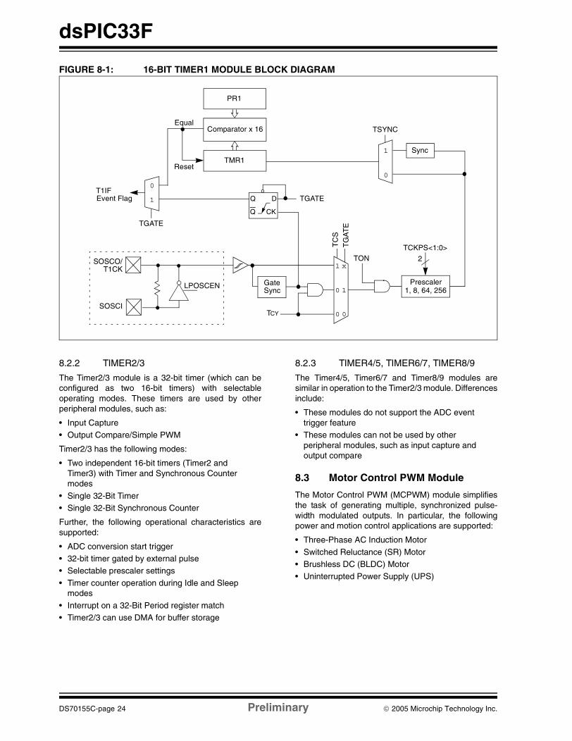
8.2.1 TIMER1
The Timer1 module (Figure 8-1) is a 16-bit timer that canserve as the time counter for an asynchronous Real-Time Clock, or operate as a free-running interval timer/counter. The 16-bit timer has the following modes:
• 16-Bit Timer• 16-Bit Synchronous Counter
• 16-Bit Asynchronous Counter
Further, the following operational characteristics aresupported:
• Timer gated by external pulse
• Selectable prescaler settings• Timer operation during CPU Idle and Sleep modes• Interrupt on 16-Bit Period register match or falling
edge of external gate signal
Timer1, when operating in Real-Time Clock (RTC)mode, provides time of day and event time-stampingcapabilities. Key operational features of the RTC are:
• Operation from 32 kHz LP oscillator• 8-bit prescaler• Low power• Real-Time Clock interrupts
© 2005 Microchip Technology Inc. Preliminary DS70155C-page 23
dsPIC33F
FIGURE 8-1: 16-BIT TIMER1 MODULE BLOCK DIAGRAM
8.2.2 TIMER2/3
The Timer2/3 module is a 32-bit timer (which can beconfigured as two 16-bit timers) with selectableoperating modes. These timers are used by otherperipheral modules, such as:
• Input Capture• Output Compare/Simple PWM
Timer2/3 has the following modes:
• Two independent 16-bit timers (Timer2 and Timer3) with Timer and Synchronous Counter modes
• Single 32-Bit Timer • Single 32-Bit Synchronous Counter
Further, the following operational characteristics aresupported:
• ADC conversion start trigger• 32-bit timer gated by external pulse• Selectable prescaler settings
• Timer counter operation during Idle and Sleep modes
• Interrupt on a 32-Bit Period register match• Timer2/3 can use DMA for buffer storage
8.2.3 TIMER4/5, TIMER6/7, TIMER8/9
The Timer4/5, Timer6/7 and Timer8/9 modules aresimilar in operation to the Timer2/3 module. Differencesinclude:
• These modules do not support the ADC event trigger feature
• These modules can not be used by other peripheral modules, such as input capture and output compare
8.3 Motor Control PWM Module
The Motor Control PWM (MCPWM) module simplifiesthe task of generating multiple, synchronized pulse-width modulated outputs. In particular, the followingpower and motion control applications are supported:
• Three-Phase AC Induction Motor
• Switched Reluctance (SR) Motor• Brushless DC (BLDC) Motor• Uninterrupted Power Supply (UPS)
TON
Sync
SOSCI
SOSCO/
PR1
T1IF
EqualComparator x 16
TMR1Reset
LPOSCEN
Event Flag
1
0
TSYNC
Q
Q D
CK
TGATE
TCKPS<1:0>
Prescaler1, 8, 64, 256
2
TGATE
TCY
1
0
T1CK
TC
S
1 x
0 1
TG
AT
E
0 0
GateSync
DS70155C-page 24 Preliminary © 2005 Microchip Technology Inc.

dsPIC33F
The PWM module has the following features:
• Dedicated time base supports TCY/2 PWM edge resolution
• Two output pins (pair) for each PWM generator• Complementary or independent operation for
each output pin pair• Hardware dead-time generators for
Complementary mode• Output pin polarity defined by nonvolatile device
configuration bits• Multiple output modes:
- Edge-Aligned mode- Center-Aligned mode- Center-Aligned mode with double updates
- Single Event mode• Manual override register for PWM output pins• Hardware Fault input pins with programmable
function• Trigger for synchronizing A/D samples and
conversions to PWM timing• Each output pin associated with the PWM can be
individually enabled
8.3.1 PWM TIME BASE
The PWM time base is provided by a 15-bit timer witha prescaler and postscaler. The PWM time base can beconfigured for four different modes of operation:
• Free-Running mode• Single-Shot mode• Continuous Up/Down Count mode
• Continuous Up/Down Count mode with interrupts for double updates
The Up/Down Counting modes support center-alignedPWM generation. The Single-Shot mode allows thePWM module to support pulse control of certainElectronically Commutated Motors (ECMs).
Table 8-1 lists the frequencies and resolutions that canbe attained as a function of the dsPIC33F deviceinstruction cycle frequency.
TABLE 8-1: EXAMPLE PWM FREQUENCIES AND RESOLUTIONS, 1:1 PRESCALER
TCY (FCY) PTPER Value PWM Resolution PWM Frequency*
25 ns (40 MHz) 0x7FFF 16 bits 1220 Hz
25 ns (40 MHz) 0x03FF 11 bits 39.1 kHz
50 ns (20 MHz) 0x7FFF 16 bits 610 Hz
50 ns (20 MHz) 0x01FF 10 bits 39.1 kHz
100 ns (10 MHz) 0x7FFF 16 bits 305 Hz
100 ns (10 MHz) 0x00FF 9 bits 39.1 kHz
200 ns (5 MHz) 0x7FFF 16 bits 153 Hz
200 ns (5 MHz) 0x007F 8 bits 39.1 kHz
* PWM frequencies will be 1/2 the value indicated for center-aligned operation.
© 2005 Microchip Technology Inc. Preliminary DS70155C-page 25

dsPIC33F
FIGURE 8-2: 8-OUTPUT PWM MODULE BLOCK DIAGRAM
PDC4
PDC4 Buffer
PWMCON1
PTPER Buffer
PWMCON2
PTPER
PTMR
Comparator
Comparator
Channel 4 Dead-TimeGenerator and
PTCON
SEVTCMP
Comparator Special Event Trigger
FLTBCON
OVDCON
PWM Enable and Mode SFRs
PWM ManualControl SFR
Channel 3 Dead-TimeGenerator and
Channel 2 Dead-TimeGenerator and
PWM Generator#3
PWM Generator#2
PWM Generator #4
SEVTDIR
PTDIR
DTCON1 Dead-Time Control SFRs
Special EventPostscaler
PWM1L
PWM1H
PWM2L
PWM2H
PWM3L
PWM3H
PWM Generator#1 Channel 1 Dead-Time
Generator and
Note: Details of PWM Generator #1, #2 and #3 are not shown for clarity.
16-B
it D
ata
Bus
PWM4L
PWM4H
DTCON2
FLTACON Fault Pin Control SFRs
PWM Time Base
OutputDriverBlock
FLTB
FLTA
Override Logic
Override Logic
Override Logic
Override Logic
DS70155C-page 26 Preliminary © 2005 Microchip Technology Inc.

dsPIC33F
8.4 Quadrature Encoder Interface (QEI) Module
Quadrature encoders (also referred to as incrementalencoders or optical encoders) are used in position andspeed detection of rotating motion systems.Quadrature encoders enable closed-loop control ofmany motor control applications, such as SwitchedReluctance (SR) Motor and AC Induction Motor(ACIM).
Typically, three outputs termed, Phase A, Phase B andINDEX, provide information that can be decoded toprovide information on the movement of the motorshaft, including distance and direction.
A quadrature decoder captures the phase signals andindex pulse and converts the information into a numericcount of the position pulses. Generally, the count will
increment when the shaft is rotating one direction anddecrement when the shaft is rotating in the otherdirection.
The QEI module (Figure 8-3) includes:
• Three input pins for two phase signals and index pulse
• Programmable digital noise filters on inputs
• Quadrature decoder providing counter pulses and count direction
• 16-bit up/down position counter• Count direction status• x2 and x4 count resolution
• Two modes of Position Counter Reset• General Purpose16-Bit Timer/Counter mode• Interrupts generated by QEI or counter events
FIGURE 8-3: QUADRATURE ENCODER INTERFACE BLOCK DIAGRAM
16-Bit Up/Down Counter
Comparator/
Max Count Register
Quadrature
ProgrammableDigital Filter
QEA
ProgrammableDigital Filter
INDX
1Up/Down
Existing Pin Logic
UPDN
3
Encoder
ProgrammableDigital Filter
QEB
Interface Logic
QEIM<2:0>Mode Select
3
(POSCNT)
(MAXCNT)
PCDOUT
QEIIFEvent Flag
Reset
Equal
2
TCY
1
0
TQCS TQCKPS<1:0>
2
1, 8, 64, 256Prescaler
Q
QD
CKTQGATE
QEIM<2:0>
Synchronize
Det
1
0
Sleep Input
0
1
UPDN_SRC
QEICON<11>Zero Detect
0
© 2005 Microchip Technology Inc. Preliminary DS70155C-page 27

dsPIC33F
8.5 Input Capture Module
The input capture module is useful in applicationsrequiring frequency (period) and pulse measurement.The dsPIC33F devices support up to eight inputcapture channels.
The input capture module captures the 16-bit value ofthe selected time base register when an event occursat the ICx pin. The events that cause a capture eventare listed below in three categories:
1. Simple Capture Event modes
- Capture timer value on every falling edge of input at ICx pin
- Capture timer value on every rising edge of input at ICx pin
2. Capture timer value on every edge (rising andfalling)
3. Prescaler Capture Event modes- Capture timer value on every 4th rising
edge of input at ICx pin- Capture timer value on every 16th rising
edge of input at ICx pin
Each input capture channel can select between one oftwo 16-bit timers (Timer2 or Timer3) for the time base.The selected timer can use either an internal or anexternal clock.
Other operational features include:
• Device wake-up from capture pin during CPU Sleep and Idle modes
• Interrupt on input capture event• 4-word FIFO buffer for capture values
- Interrupt optionally generated after 1, 2, 3 or 4 buffer locations are filled
• Input capture can also be used to provide additional sources of external interrupts.
Input capture channels IC1 and IC2 support DMA datatransfers.
8.6 Output Compare/PWM Module
The output compare module features are quite usefulin applications that require controlled timing pulses orPWM modulated pulse streams.
The output compare module has the ability to comparethe value of a selected time base with the value of oneor two compare registers (depending on the operationmode selected). Furthermore, it has the ability togenerate a single output pulse, or a repetitivesequence of output pulses, on a compare match event.Like most dsPIC33F peripherals, it also has the abilityto generate interrupts on compare match events.
The dsPIC33F device may have up to eight outputcompare channels, designated OC1 through OC8.Refer to the specific device data sheet for the numberof channels available in a particular device. All outputcompare channels are functionally identical.
Each output compare channel can use one of twoselectable time bases. The time base is selected usingthe OCTSEL bit (OCxCON<3>). An ‘x’ in the pin,register or bit name denotes the specific outputcompare channel. Refer to the device data sheet for thespecific timers that can be used with each outputcompare channel number.
Each output compare module has the following modesof operation:
• Single Compare Match mode
• Dual Compare Match mode generating- Single Output Pulse- Continuous Output Pulses
• Simple Pulse-Width Modulation mode- With Fault Protection Input - Without Fault Protection Input
Output compare channels, OC1 and OC2, supportDMA data transfers.
8.7 Data Converter Interface Module
The dsPIC33F Data Converter Interface (DCI) moduleallows simple interfacing to devices such as audiocoder/decoders (codecs), A/D Converters and D/AConverters.
The following interfaces are supported:
• Framed Synchronous Serial Transfer (Single or Multi-Channel)
• Inter-IC Sound (I2S) Interface• AC-Link (AC’97) Compliant mode
Many codecs intended for use in audio applicationssupport sampling rates between 8 kHz and 48 kHz anduse one of the interface protocols listed above. TheDCI automatically handles the interface timingassociated with these codecs. No overhead from theCPU is required until the requested amount of data hasbeen transmitted and/or received by the DCI. Up to fourdata words can be transferred between CPU interrupts.
The data word length for the DCI is programmable upto 16 bits to match the data size of the dsPIC33F CPU.However, many codecs have data word sizes greaterthan 16 bits. Long data word lengths can be supportedby the DCI. The DCI is configured to transmit/receivethe long word in multiple 16-bit time slots. Thisoperation is transparent to the user and the long dataword is stored in consecutive register locations.
DS70155C-page 28 Preliminary © 2005 Microchip Technology Inc.

dsPIC33F
Figure 8-4 is a block diagram of the DCI module. TheDCI can support up to 16 time slots in a data frame fora maximum frame size of 256 bits. There are control
bits for each time slot in the data frame that determinewhether the DCI will transmit/receive during the timeslot. The DCI module supports DMA data transfers.
FIGURE 8-4: DCI MODULE BLOCK DIAGRAM
8.8 SPI™ Module
The Serial Peripheral Interface (SPI) module is asynchronous serial interface for communicating withother peripheral or microcontroller devices such asserial EEPROMs, shift registers, display drivers, A/DConverters, etc. It is compatible with Motorola® SPI andSIOP interfaces.
This SPI module includes all SPI modes. A FrameSynchronization mode is also included for support ofvoice band codecs.
Four pins make up the serial interface: SDI, Serial DataInput; SDO, Serial Data Output; SCK, Shift Clock Inputor Output; SS, Active-Low Slave Select, which alsoserves as the FSYNC (Frame Synchronization Pulse).A device set up as an SPI master provides the serialcommunication clock signal on its SCK pin.
A series of 8 or 16 clock pulses (depending on mode)shift out the 8 or 16 bits (depending on whether a byteor word is being transferred) and simultaneously shift in8 or 16 bits of data from the SDI pin. An interrupt isgenerated when the transfer is complete.
Slave select synchronization allows selective enablingof SPI slave devices, which is particularly useful whena single master is connected to multiple slaves.
The SPI1 and SPI2 modules support DMA datatransfers.
BCG Control Bits
16-B
it D
ata
Bus
Sample Rate Generator
CSCKD
COFSD
DCI Buffer
Frame Synchronization
Generator
Control Unit
DCI Shift Register
Receive Buffer Registers w/Shadow
FOSC/4
Word Size Selection bits
Frame Length Selection bits
DCI Mode Selection bits
CSCK
COFS
CSDI
CSDO
15 0Transmit Buffer Registers w/Shadow
© 2005 Microchip Technology Inc. Preliminary DS70155C-page 29

dsPIC33F
DS
8.9 UART Module
The UART is a full-duplex asynchronous system thatcan communicate with peripheral devices, such aspersonal computers, RS-232 and RS-485 interfaces.
The dsPIC33F devices have one or more UARTs.
The key features of the UART module are:
• Full-duplex operation with 8 or 9-bit data• Even, odd or no parity options (for 8-bit data)• One or two Stop bits
• Fully integrated Baud Rate Generator (BRG) with 16-bit prescaler
• Baud rates range from up to 10 Mbps and down to 38 Hz at 40 MIPS
• 4-character deep transmit data buffer• 4-character deep receive data buffer• Parity, framing and buffer overrun error detection
• Full IrDA® support, including hardware encoding and decoding of IrDA® messages
• LIN bus support- Auto wake-up from Sleep or Idle mode on
Start bit detect - Auto-baud detection- Break character support
• Support for interrupt on address detect (9th bit = 1)• Separate transmit and receive interrupts
- On transmission of 1 or 4 characters
- On reception of 1, 3 and 4 characters• Loopback mode for diagnostics
The UART1 and UART2 modules support DMA datatransfers.
8.10 I2C™ Module
The I2C module is a synchronous serial interface, usefulfor communicating with other peripheral ormicrocontroller devices. These peripheral devices maybe serial EEPROMs, shift registers, display drivers, A/DConverters, etc.
The Inter-Integrated Circuit (I2C) module offers fullhardware support for both slave and multi-masteroperations.
The key features of the I2C module are:
• I2C slave operation supports 7 and 10-bit address• I2C master operation supports 7 and 10-bit address• I2C port allows bidirectional transfers between
master and slaves• Serial clock synchronization for I2C port can be
used as a handshake mechanism to suspend and resume serial transfer (serial clock stretching)
• I2C supports multi-master operation; detects bus collision and will arbitrate accordingly
• Slew rate control for 100 kHz and 400 kHz bus speeds
In I2C mode, pin SCL is clock and pin SDA is data. Themodule will override the data direction bits for these pins.
8.11 Controller Area Network (CAN) Module
The Controller Area Network (CAN) module is a serialinterface useful for communicating with other CANmodules or microcontroller devices. This interface/protocol was designed to allow communications withinnoisy environments.
The CAN module is a communication controllerimplementing the CAN 2.0 A/B protocol, as defined inthe BOSCH specification. The module supportsCAN 1.2, CAN 2.0A, CAN2.0B Passive and CAN 2.0BActive versions of the protocol. Details of these protocolscan be found in the BOSCH CAN specification.
The CAN module features:
• Implementation of the CAN protocol CAN 1.2, CAN 2.0A and CAN 2.0B
• Standard and extended data frames• Data lengths of 0-8 bytes
• Programmable bit rate up to 1 Mbit/sec• Automatic response to remote frames• Up to 16 receive buffers in DMA RAM
• FIFO Buffer mode (up to 64 messages deep)• 16 full (standard/extended identifier) acceptance
filters• 3 full acceptance filter masks• Up to 8 transmit buffers in DMA RAM
• DMA can be used for transmission and reception• Programmable wake-up functionality with
integrated low-pass filter• Programmable Loopback mode supports self-test
operation• Signaling via interrupt capabilities for all CAN
receiver and transmitter error states• Programmable clock source• Programmable link to timer module for
time-stamping and network synchronization• Low-power Sleep and Idle mode
The CAN bus module consists of a protocol engine andmessage buffering/control. The CAN protocol enginehandles all functions for receiving and transmittingmessages on the CAN bus. Messages are transmittedby first loading the appropriate data registers. Statusand errors can be checked by reading the appropriateregisters. Any message detected on the CAN bus ischecked for errors and then matched against filters tosee if it should be received and stored in one of thereceive registers.
70155C-page 30 Preliminary © 2005 Microchip Technology Inc.

dsPIC33F
8.12 I/O Pins
Some pins for the I/O pin functions are multiplexed withan alternate function for the peripheral features on thedevice. In general, when a peripheral is enabled, thatpin may not be used as a general purpose I/O pin.
All I/O port pins have three registers directly associatedwith the operation of the port pin. The Data Directionregister determines whether the pin is an input or anoutput. The Port Data Latch register provides latchedoutput data for the I/O pins. The Port register providesvisibility of the logic state of the I/O pins. Reading thePort register provides the I/O pin logic state, whilewrites to the Port register write the data to the Port DataLatch register.
I/O port pins have latch bits (Port Data Latch register).This register, when read, yields the contents of the I/Olatch and when written, modifies the contents of the I/Olatch, thus modifying the value driven out on a pin if thecorresponding Data Direction register bit is configuredfor output. This can be used in read-modify-writeinstructions that allow the user to modify the contentsof the Port Data Latch register, regardless of the statusof the corresponding pins.
The I/O pins have the following features:
• Schmitt Trigger input• CMOS output drivers
• Weak internal pull-up
All I/O pins configured as digital inputs can accept 5Vsignals. This provides a degree of compatibility withexternal signals of different voltage levels. However, alldigital outputs and analog pins can only generatevoltage levels up to 3.6V.
The input change notification module gives dsPIC33Fdevices the ability to generate interrupt requests to theprocessor in response to a change of state on selectedinput pins. This module is capable of detecting inputchanges of state, even in Sleep mode, when the clocksare disabled. There are up to 24 external signals (CN0through CN23) that can be selected (enabled) forgenerating an interrupt request on a change of state.Each of the CN pins also has an optional weak pull-upfeature.
© 2005 Microchip Technology Inc. Preliminary DS70155C-page 31

dsPIC33F
9.0 dsPIC33F INSTRUCTION SET
9.1 Introduction
The dsPIC33F instruction set provides a broad suite ofinstructions which supports traditional microcontrollerapplications, and a class of instructions which supportsmath-intensive applications. Since almost all of thefunctionality of the PICmicro® MCU instruction set hasbeen maintained, this hybrid instruction set allows afriendly DSP migration path for users already familiarwith the PICmicro microcontroller.
9.2 Instruction Set Overview
The dsPIC33F instruction set contains 84 instructionswhich can be grouped into the ten functional categoriesshown in Table 9-1. Table 9-2 defines the symbolsused in the instruction summary tables, Table 9-3through Table 9-12. These tables define the syntax,description, storage and execution requirementsfor each instruction. Storage requirements are repre-sented in 24-bit instruction words and executionrequirements are represented in instruction cycles.Most instructions have several different addressingmodes and execution flows which require differentinstruction variants. For instance, there are six uniqueADD instructions and each instruction variant has itsown instruction encoding.
TABLE 9-1: dsPIC33F INSTRUCTION GROUPS
9.2.1 MULTI-CYCLE INSTRUCTIONS
As the instruction summary tables show, mostinstructions execute in a single cycle with the followingexceptions:
• Instructions DO, MOV.D, POP.D, PUSH.D, TBLRDH, TBLRDL, TBLWTH and TBLWTL require 2 cycles to execute.
• Instructions DIVF, DIV.S, DIV.U are single-cycle instructions, which should be executed 18 consecutive times as the target REPEAT instruction.
• Instructions that change the program counter also require 2 cycles to execute, with the extra cycle executed as a NOP. Skip instructions, which skip over a 2-word instruction, require 3 instruction cycles to execute with 2 cycles executed as a NOP.
• The RETFIE, RETLW and RETURN are special cases of instructions that change the program counter. These execute in 3 cycles unless an exception is pending, and then they execute in 2 cycles.
9.2.2 MULTI-WORD INSTRUCTIONS
As the instruction summary tables show, almost allinstructions consume one instruction word (24 bits),with the exception of the CALL, DO and GOTOinstructions, which are flow instructions listed inTable 9-9. These instructions require two words ofmemory because their opcodes embed large literaloperands.
Functional Group Summary Table
Move Instructions Table 9-3
Math Instructions Table 9-4
Logic Instructions Table 9-5
Rotate/Shift Instructions Table 9-6
Bit Instructions Table 9-7
Compare/Skip Instructions Table 9-8
Program Flow Instructions Table 9-9
Shadow/Stack Instructions Table 9-10
Control Instructions Table 9-11
DSP Instructions Table 9-12
Note: Instructions that access program memoryas data, using Program Space Visibility,incur some cycle count overhead.
DS70155C-page 32 Preliminary © 2005 Microchip Technology Inc.

dsPIC33F
TABLE 9-2: SYMBOLS USED IN SUMMARY TABLES
Symbol Description
# Literal operand designation
Acc Accumulator A or Accumulator B
AWB Accumulator Write Back
bit4 4-bit wide bit position (0:15)
Expr Absolute address, label or expression (resolved by the linker)
f File register address
lit1 1-bit literal (0:1)
lit4 4-bit literal (0:15)
lit5 5-bit literal (0:31)
lit8 8-bit literal (0:255)
lit10 10-bit literal (0:255 for Byte mode, 0:1023 for Word mode)
lit14 14-bit literal (0:16383)
lit16 16-bit literal (0:65535)
lit23 23-bit literal (0:8388607)
Slit4 Signed 4-bit literal (-8:7)
Slit6 Signed 6-bit literal (-16:16)
Slit10 Signed 10-bit literal (-512:511)
Slit16 Signed 16-bit literal (-32768:32767)
TOS Top-of-Stack
Wb Base working register
Wd Destination working register (direct and indirect addressing)
Wm, Wn Working register divide pair (dividend, divisor)
Wm*Wm Working register multiplier pair (same source register)
Wm*Wn Working register multiplier pair (different source registers)
Wn Both source and destination working register (direct addressing)
Wnd Destination working register (direct addressing)
Wns Source working register (direct addressing)
WREG Default working register
Ws Source working register (direct and indirect addressing)
Wx Source addressing mode and working register for X data bus prefetch
Wxd Destination working register for X data bus prefetch
Wy Source addressing mode and working register for Y data bus prefetch
Wyd Destination working register for Y data bus prefetch
© 2005 Microchip Technology Inc. Preliminary DS70155C-page 33

dsPIC33F
TABLE 9-3: MOVE INSTRUCTIONS
Assembly Syntax Description Words Cycles
EXCH Wns,Wnd Swap Wns and Wnd 1 1
MOV f {,WREG} Move f to destination 1 1
MOV WREG,f Move WREG to f 1 1
MOV f,Wnd Move f to Wnd 1 1
MOV Wns,f Move Wns to f 1 1
MOV.b #lit8,Wnd Move 8-bit literal to Wnd 1 1
MOV #lit16,Wnd Move 16-bit literal to Wnd 1 1
MOV [Ws+Slit10],Wnd Move [Ws + signed 10-bit offset] to Wnd 1 1
MOV Wns,[Wd+Slit10] Move Wns to [Wd + signed 10-bit offset] 1 1
MOV Ws,Wd Move Ws to Wd 1 1
MOV.D Ws,Wnd Move double Ws to Wnd:Wnd + 1 1 2
MOV.D Wns,Wd Move double Wns:Wns + 1 to Wd 1 2
SWAP Wn Wn = byte or nibble swap Wn 1 1
TBLRDH Ws,Wd Read high program word to Wd 1 2
TBLRDL Ws,Wd Read low program word to Wd 1 2
TBLWTH Ws,Wd Write Ws to high program word 1 2
TBLWTL Ws,Wd Write Ws to low program word 1 2
Note: When the optional {,WREG} operand is specified, the destination of the instruction is WREG. When{,WREG} is not specified, the destination of the instruction is the file register f.
Note: Table 9-3 through Table 9-12 present the base instruction syntax for the dsPIC33F. These instructions do notinclude all of the available addressing modes. For example, some instructions show the Byte Addressingmode and others do not.
DS70155C-page 34 Preliminary © 2005 Microchip Technology Inc.

dsPIC33F
TABLE 9-4: MATH INSTRUCTIONS
Assembly Syntax Description Words Cycles
ADD f {,WREG} Destination = f + WREG 1 1
ADD #lit10,Wn Wn = lit10 + Wn 1 1ADD Wb,#lit5,Wd Wd = Wb + lit5 1 1ADD Wb,Ws,Wd Wd = Wb + Ws 1 1
ADDC f {,WREG} Destination = f + WREG + (C) 1 1ADDC #lit10,Wn Wn = lit10 + Wn + (C) 1 1ADDC Wb,#lit5,Wd Wd = Wb + lit5 + (C) 1 1
ADDC Wb,Ws,Wd Wd = Wb + Ws + (C) 1 1DAW.B Wn Wn = decimal adjust Wn 1 1DEC f {,WREG} Destination = f – 1 1 1
DEC Ws,Wd Wd = Ws – 1 1 1DEC2 f {,WREG} Destination = f – 2 1 1DEC2 Ws,Wd Wd = Ws – 2 1 1
DIV.S Wm,Wn Signed 16/16-bit integer divide* 1 18DIV.SD Wm,Wn Signed 32/16-bit integer divide* 1 18DIV.U Wm,Wn Unsigned 16/16-bit integer divide* 1 18
DIV.UD Wm,Wn Unsigned 32/16-bit integer divide* 1 18DIVF Wm,Wn Signed 16/16-bit fractional divide* 1 18INC f {,WREG} Destination = f + 1 1 1
INC Ws,Wd Wd = Ws + 1 1 1INC2 f {,WREG} Destination = f + 2 1 1INC2 Ws,Wd Wd = Ws + 2 1 1
MUL f W3:W2 = f * WREG 1 1MUL.SS Wb,Ws,Wnd {Wnd + 1,Wnd} = sign(Wb) * sign(Ws) 1 1
MUL.SU Wb,#lit5,Wnd {Wnd + 1,Wnd} = sign(Wb) * unsign(lit5) 1 1MUL.SU Wb,Ws,Wnd {Wnd + 1,Wnd} = sign(Wb) * unsign(Ws) 1 1MUL.US Wb,Ws,Wnd {Wnd + 1,Wnd} = unsign(Wb) * sign(Ws) 1 1
MUL.UU Wb,#lit5,Wnd {Wnd + 1,Wnd} = unsign(Wb) * unsign(lit5) 1 1MUL.UU Wb,Ws,Wnd {Wnd + 1,Wnd} = unsign(Wb) * unsign(Ws) 1 1SE Ws,Wnd Wnd = sign-extended Ws 1 1
SUB f {,WREG} Destination = f – WREG 1 1SUB #lit10, Wn Wn = Wn – lit10 1 1SUB Wb,#lit5,Wd Wd = Wb – lit5 1 1
SUB Wb,Ws,Wd Wd = Wb – Ws 1 1SUBB f {,WREG} Destination = f – WREG – (C) 1 1SUBB #lit10, Wn Wn = Wn – lit10 – (C) 1 1
SUBB Wb,#lit5,Wd Wd = Wb – lit5 – (C) 1 1
SUBB Wb,Ws,Wd Wd = Wb – Ws – (C) 1 1
SUBBR f {,WREG} Destination = WREG – f – (C) 1 1
SUBBR Wb,#lit5,Wd Wd = lit5 – Wb – (C) 1 1
SUBBR Wb,Ws,Wd Wd = Ws – Wb – (C) 1 1SUBR f {,WREG} Destination = WREG – f 1 1SUBR Wb,#lit5,Wd Wd = lit5 – Wb 1 1
SUBR Wb,Ws,Wd Wd = Ws – Wb 1 1ZE Ws,Wnd Wnd = zero-extended Ws 1 1* Divide instructions are interruptible on a cycle-by-cycle basis. Also, divide instructions must be accompanied by a REPEAT instruction, which adds 1 extra cycle.
© 2005 Microchip Technology Inc. Preliminary DS70155C-page 35
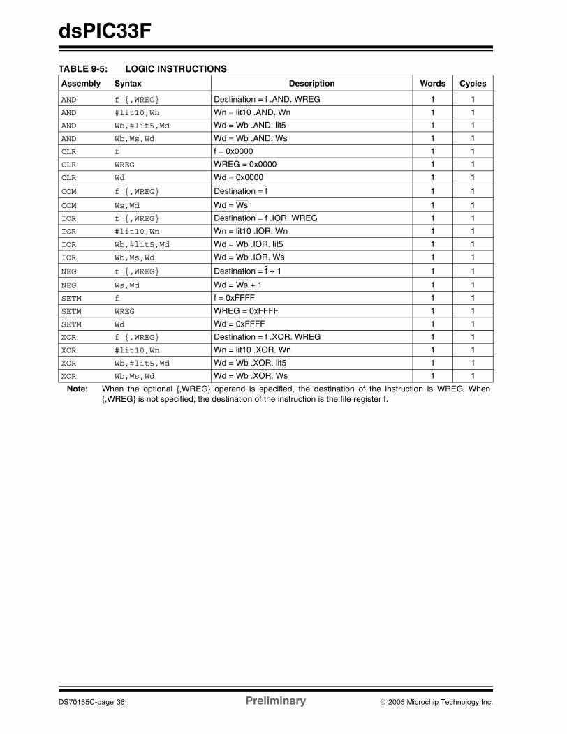
dsPIC33F
TABLE 9-5: LOGIC INSTRUCTIONS
Assembly Syntax Description Words Cycles
AND f {,WREG} Destination = f .AND. WREG 1 1
AND #lit10,Wn Wn = lit10 .AND. Wn 1 1
AND Wb,#lit5,Wd Wd = Wb .AND. lit5 1 1
AND Wb,Ws,Wd Wd = Wb .AND. Ws 1 1
CLR f f = 0x0000 1 1
CLR WREG WREG = 0x0000 1 1
CLR Wd Wd = 0x0000 1 1
COM f {,WREG} Destination = f 1 1
COM Ws,Wd Wd = Ws 1 1
IOR f {,WREG} Destination = f .IOR. WREG 1 1
IOR #lit10,Wn Wn = lit10 .IOR. Wn 1 1
IOR Wb,#lit5,Wd Wd = Wb .IOR. lit5 1 1
IOR Wb,Ws,Wd Wd = Wb .IOR. Ws 1 1
NEG f {,WREG} Destination = f + 1 1 1
NEG Ws,Wd Wd = Ws + 1 1 1
SETM f f = 0xFFFF 1 1
SETM WREG WREG = 0xFFFF 1 1
SETM Wd Wd = 0xFFFF 1 1
XOR f {,WREG} Destination = f .XOR. WREG 1 1
XOR #lit10,Wn Wn = lit10 .XOR. Wn 1 1
XOR Wb,#lit5,Wd Wd = Wb .XOR. lit5 1 1
XOR Wb,Ws,Wd Wd = Wb .XOR. Ws 1 1
Note: When the optional {,WREG} operand is specified, the destination of the instruction is WREG. When{,WREG} is not specified, the destination of the instruction is the file register f.
DS70155C-page 36 Preliminary © 2005 Microchip Technology Inc.

dsPIC33F
TABLE 9-6: ROTATE/SHIFT INSTRUCTIONS
TABLE 9-7: BIT INSTRUCTIONS
Assembly Syntax Description Words Cycles
ASR f {,WREG} Destination = arithmetic right shift f 1 1
ASR Ws,Wd Wd = arithmetic right shift Ws 1 1
ASR Wb,#lit4,Wnd Wnd = arithmetic right shift Wb by lit4 1 1
ASR Wb,Wns,Wnd Wnd = arithmetic right shift Wb by Wns 1 1
LSR f {,WREG} Destination = logical right shift f 1 1
LSR Ws,Wd Wd = logical right shift Ws 1 1
LSR Wb,#lit4,Wnd Wnd = logical right shift Wb by lit4 1 1
LSR Wb,Wns,Wnd Wnd = logical right shift Wb by Wns 1 1
RLC f {,WREG} Destination = rotate left through Carry f 1 1
RLC Ws,Wd Wd = rotate left through Carry Ws 1 1
RLNC f {,WREG} Destination = rotate left (no Carry) f 1 1
RLNC Ws,Wd Wd = rotate left (no Carry) Ws 1 1
RRC f {,WREG} Destination = rotate right through Carry f 1 1
RRC Ws,Wd Wd = rotate right through Carry Ws 1 1
RRNC f {,WREG} Destination = rotate right (no Carry) f 1 1
RRNC Ws,Wd Wd = rotate right (no Carry) Ws 1 1
SL f {,WREG} Destination = left shift f 1 1
SL Ws,Wd Wd = left shift Ws 1 1
SL Wb,#lit4,Wnd Wnd = left shift Wb by lit4 1 1
SL Wb,Wns,Wnd Wnd = left shift Wb by Wns 1 1
Note: When the optional {,WREG} operand is specified, the destination of the instruction is WREG. When{,WREG} is not specified, the destination of the instruction is the file register f.
Assembly Syntax Description Words Cycles
BCLR f,#bit4 Bit clear f 1 1
BCLR Ws,#bit4 Bit clear Ws 1 1
BSET f,#bit4 Bit set f 1 1
BSET Ws,#bit4 Bit set Ws 1 1
BSW.C Ws,Wb Write C bit to Ws<Wb> 1 1
BSW.Z Ws,Wb Write SZ bit to Ws<Wb> 1 1
BTG f,#bit4 Bit toggle f 1 1
BTG Ws,#bit4 Bit toggle Ws 1 1
BTST f,#bit4 Bit test f 1 1
BTST.C Ws,#bit4 Bit test Ws to C 1 1
BTST.Z Ws,#bit4 Bit test Ws to SZ 1 1
BTST.C Ws,Wb Bit test Ws<Wb> to C 1 1
BTST.Z Ws,Wb Bit test Ws<Wb> to SZ 1 1
BTSTS f,#bit4 Bit test f then set f 1 1
BTSTS.C Ws,#bit4 Bit test Ws to C then set Ws 1 1
BTSTS.Z Ws,#bit4 Bit test Ws to SZ then set Ws 1 1
FBCL Ws,Wnd Find bit change from left (MSb) side 1 1
FF1L Ws,Wnd Find first one from left (MSb) side 1 1
FF1R Ws,Wnd Find first one from right (LSb) side 1 1
Note: Bit positions are specified by bit4 (0:15) for word operations.
© 2005 Microchip Technology Inc. Preliminary DS70155C-page 37

dsPIC33F
TABLE 9-8: COMPARE/SKIP INSTRUCTIONS
Assembly Syntax Description Words Cycles
BTSC f,#bit4 Bit test f, skip if clear 1 1 (2 or 3)
BTSC Ws,#bit4 Bit test Ws, skip if clear 1 1 (2 or 3)
BTSS f,#bit4 Bit test f, skip if set 1 1 (2 or 3)
BTSS Ws,#bit4 Bit test Ws, skip if set 1 1 (2 or 3)
CP f Compare (f – WREG) 1 1
CP Wb,#lit5 Compare (Wb – lit5) 1 1
CP Wb,Ws Compare (Wb – Ws) 1 1
CP0 f Compare (f – 0x0000) 1 1
CP0 Ws Compare (Ws – 0x0000) 1 1
CPB f Compare with Borrow (f – WREG – C) 1 1
CPB Wb,#lit5 Compare with Borrow (Wb – lit5 – C) 1 1
CPB Wb,Ws Compare with Borrow (Wb – Ws – C) 1 1
CPSEQ Wb,Wn Compare Wb with Wn, Skip if Equal (Wb = Wn) 1 1 (2 or 3)
CPSGT Wb,Wn Signed Compare Wb with Wn, Skip if Greater Than (Wb > Wn) 1 1 (2 or 3)
CPSLT Wb,Wn Signed Compare Wb with Wn, Skip if Less Than (Wb < Wn) 1 1 (2 or 3)
CPSNE Wb,Wn Signed Compare Wb with Wn, Skip if Not Equal (Wb ≠ Wn) 1 1 (2 or 3)
Note 1: Bit positions are specified by bit4 (0:15) for word operations.2: Conditional skip instructions execute in 1 cycle if the skip is not taken, 2 cycles if the skip is taken over a
one-word instruction and 3 cycles if the skip is taken over a two-word instruction.
DS70155C-page 38 Preliminary © 2005 Microchip Technology Inc.

dsPIC33F
TABLE 9-9: PROGRAM FLOW INSTRUCTIONS
Assembly Syntax Description Words Cycles
BRA Expr Branch unconditionally 1 2
BRA Wn Computed branch 1 2
BRA C,Expr Branch if Carry (no Borrow) 1 1 (2)
BRA GE,Expr Branch if greater than or equal 1 1 (2)
BRA GEU,Expr Branch if unsigned greater than or equal 1 1 (2)
BRA GT,Expr Branch if greater than 1 1 (2)
BRA GTU,Expr Branch if unsigned greater than 1 1 (2)
BRA LE,Expr Branch if less than or equal 1 1 (2)
BRA LEU,Expr Branch if unsigned less than or equal 1 1 (2)
BRA LT,Expr Branch if less than 1 1 (2)
BRA LTU,Expr Branch if unsigned less than 1 1 (2)
BRA N,Expr Branch if Negative 1 1 (2)
BRA NC,Expr Branch if not Carry (Borrow) 1 1 (2)
BRA NN,Expr Branch if not Negative 1 1 (2)
BRA NOV,Expr Branch if not Overflow 1 1 (2)
BRA NZ,Expr Branch if not Zero 1 1 (2)
BRA OA,Expr Branch if Accumulator A Overflow 1 1 (2)
BRA OB,Expr Branch if Accumulator B Overflow 1 1 (2)
BRA OV,Expr Branch if Overflow 1 1 (2)
BRA SA,Expr Branch if Accumulator A Saturate 1 1 (2)
BRA SB,Expr Branch if Accumulator B Saturate 1 1 (2)
BRA Z,Expr Branch if Zero 1 1 (2)
CALL Expr Call subroutine 2 2
CALL Wn Call indirect subroutine 1 2
DO #lit14,Expr Do code through PC + Expr, (lit14 + 1) times 2 2
DO Wn,Expr Do code through PC + Expr, (Wn + 1) times 2 2
GOTO Expr Go to address 2 2
GOTO Wn Go to address indirectly 1 2
RCALL Expr Relative call 1 2
RCALL Wn Computed call 1 2
REPEAT #lit14 Repeat next instruction (lit14 + 1) times 1 1
REPEAT Wn Repeat next instruction (Wn + 1) times 1 1
RETFIE Return from interrupt enable 1 3 (2)
RETLW #lit10,Wn Return with lit10 in Wn 1 3 (2)
RETURN Return from subroutine 1 3 (2)
Note 1: Conditional branch instructions execute in 1 cycle if the branch is not taken, or 2 cycles if the branch is taken.
2: RETURN normally executes in 3 cycles; however, it executes in 2 cycles if an interrupt is pending.
© 2005 Microchip Technology Inc. Preliminary DS70155C-page 39

dsPIC33F
TABLE 9-10: SHADOW/STACK INSTRUCTIONS
TABLE 9-11: CONTROL INSTRUCTIONS
TABLE 9-12: DSP INSTRUCTIONS
Assembly Syntax Description Words Cycles
LNK #lit14 Link Frame Pointer 1 1
POP f Pop TOS to f 1 1
POP Wd Pop TOS to Wd 1 1
POP.D Wnd Double pop from TOS to Wnd:Wnd + 1 1 2
POP.S Pop shadow registers 1 1
PUSH f Push f to TOS 1 1
PUSH Ws Push Ws to TOS 1 1
PUSH.D Wns Push double Wns:Wns + 1 to TOS 1 2
PUSH.S Push shadow registers 1 1
ULNK Unlink Frame Pointer 1 1
Assembly Syntax Description Words Cycles
CLRWDT Clear Watchdog Timer 1 1
DISI #lit14 Disable interrupts for (lit14 + 1) instruction cycles 1 1
NOP No operation 1 1
NOPR No operation 1 1
PWRSAV #lit1 Enter Power-Saving mode lit1 1 1
RESET Software device Reset 1 1
Assembly Syntax Description Words Cycles
ADD Acc Add accumulators 1 1
ADD Ws,#Slit4,Acc 16-bit signed add to Acc 1 1
CLR Acc,Wx,Wxd,Wy,Wyd,AWB Clear Acc 1 1
ED Wm*Wm,Acc,Wx,Wy,Wxd Euclidean distance (no accumulate) 1 1
EDAC Wm*Wm,Acc,Wx,Wy,Wxd Euclidean distance 1 1
LAC Ws,#Slit4,Acc Load Acc 1 1
MAC Wm*Wn,Acc,Wx,Wxd,Wy,Wyd,AWB Multiply and accumulate 1 1
MAC Wm*Wm,Acc,Wx,Wxd,Wy,Wyd Square and accumulate 1 1
MOVSAC Acc,Wx,Wxd,Wy,Wyd,AWB Move Wx to Wxd and Wy to Wyd 1 1
MPY Wm*Wn,Acc,Wx,Wxd,Wy,Wyd Multiply Wn by Wm to Acc 1 1
MPY Wm*Wm,Acc,Wx,Wxd,Wy,Wyd Square to Acc 1 1
MPY.N Wm*Wn,Acc,Wx,Wxd,Wy,Wyd -(Multiply Wn by Wm) to Acc 1 1
MSC Wm*Wn,Acc,Wx,Wxd,Wy,Wyd,AWB Multiply and subtract from Acc 1 1
NEG Acc Negate Acc 1 1
SAC Acc,#Slit4,Wd Store Acc 1 1
SAC.R Acc,#Slit4,Wd Store rounded Acc 1 1
SFTAC Acc,#Slit6 Arithmetic shift Acc by Slit6 1 1
SFTAC Acc,Wn Arithmetic shift Acc by (Wn) 1 1
SUB Acc Subtract accumulators 1 1
DS70155C-page 40 Preliminary © 2005 Microchip Technology Inc.

dsPIC33F
10.0 MICROCHIP DEVELOPMENT TOOL SUPPORT
Microchip offers comprehensive development toolsand libraries to support the dsPIC33F architecture. Inaddition, the company is partnering with many thirdparty tools manufacturers for additional dsPIC33Fdevice support. Table 10-1 lists development tools thatsupport the dsPIC33F family. The paragraphs thatfollow describe each of the tools in more detail.
TABLE 10-1: dsPIC33F DEVELOPMENT TOOLSDevelopment Tool Description Part # From
Ess
enti
al
So
ftw
are
Too
ls
MPLAB® IDE (see Section 10.1 MPLAB Inte-grated Development Environment Software)
Integrated Development Environment SW007002 Microchip
MPLAB ASM30(see Section 10.2 MPLAB ASM30 Assembler/Linker/Librarian)
Assembler (included in MPLAB IDE) SW007002 Microchip
MPLAB SIM(see Section 10.3 MPLAB SIM Software Simulator)
Software Simulator (Included in MPLAB IDE) SW007002 Microchip
MPLAB VDI(see Section 10.4 MPLAB Visual Device Initializer)
Visual Device Initializer for dsPIC33F(included in MPLAB IDE)
SW007002 Microchip
MPLAB C30(see Section 10.5 MPLAB C30 C Compiler/Linker/Librarian)
ANSI C Compiler, Assembler, Linker and Librarian SW006012 Microchip
Ess
enti
al
Har
dw
are
Too
ls
MPLAB ICD 2(see Section 10.6 MPLAB ICD 2 In-Circuit Debugger)
In-Circuit Debugger and Device Programmer DV164005 Microchip
MPLAB PM3(see Section 10.7 MPLAB PM3 Universal Device Programmer)
Full-Featured Device Programmer, Base Unit DV007004 Microchip
Socket Module for 100L TQFP Devices (14 mm x 14 mm) TBD Microchip
Socket Module for 80L TQFP Devices (12 mm x 12 mm) TBD Microchip
Socket Module for 64L TQFP Devices (10 mm x 10 mm) TBD Microchip
Legend: TBD = To Be Determined
© 2005 Microchip Technology Inc. Preliminary DS70155C-page 41

dsPIC33F
10.1 MPLAB Integrated Development Environment Software
The MPLAB Integrated Development Environment(IDE) is available at no cost. The MPLAB IDE lets theuser edit, compile and emulate from a single userinterface, as depicted in Figure 10-1. Code can bedesigned and developed for the dsPIC® DSC devicesin the same design environment as the PICmicromicrocontrollers. The MPLAB IDE is a 32-bit Windows®
operating system-based application that providesmany advanced features for the demanding engineer ina modern, easy-to-use interface. MPLAB IDEintegrates:
• Full-featured, color coded text editor• Easy to use project manager with visual display• Source level debugging
• Enhanced source level debugging for ‘C’ (structures, automatic variables, etc.)
• Customizable toolbar and key mapping• Dynamic status bar displays processor condition
• Context sensitive, interactive on-line help• Integrated MPLAB SIM instruction simulator
• User interface for MPLAB PM3 and PICSTART® Plus device programmers (sold separately)
• User interface for MPLAB ICD 2 In-Circuit Debugger (sold separately)
The MPLAB IDE allows:
• Editing of source files in either assembly or ‘C’
• One-touch compiling and downloading to dsPIC DSC emulator or simulator
• Debugging using:- Source files- Machine code
- Mixed mode source and machine code
The ability to use the MPLAB IDE with multipledevelopment and debugging targets provides easytransition from the cost-effective simulator to MPLABICD 2, or to a full-featured emulator with minimalretraining.
FIGURE 10-1: MPLAB® IDE DESKTOP
Powerful Project Manager handles
multiple projects and all file types
Color keyed editor makes
source code debug easier
Status bar updates on
single step or run
Set break/trace points with
a click of the mouse
Fully customizable watch windows
to view and modify registers and
memory locations
Simply move your mouse over a
variable to view or modify
DS70155C-page 42 Preliminary © 2005 Microchip Technology Inc.

dsPIC33F
10.2 MPLAB ASM30 Assembler/Linker/Librarian
MPLAB ASM30 is a full-featured macro assembler.User-defined macros, conditional assembly and avariety of assembler directives make the MPLABASM30 a powerful code generation tool.
The accompanying MPLAB LINK30 Linker and MPLABLIB30 Librarian modules allow efficient linking, librarycreation and maintenance.
Notable features of the assembler include:
• Support for the entire dsPIC DSC instruction set• Support for fixed-point and floating-point data
• Available for Windows operating system• Command Line Interface• Rich Directive Set
• Flexible Macro Language• MPLAB IDE compatibility
Notable features of the linker include:
• Automatic or user-defined stack allocation• Supports dsPIC DSC Program Space Visibility
(PSV) window• Available for Windows operating systems
• Command Line Interface• Linker scripts for all dsPIC DSC devices• MPLAB IDE compatibility
10.3 MPLAB SIM Software Simulator
The MPLAB SIM software simulator provides codedevelopment for the dsPIC33F family in a PC-hostedenvironment by simulating the dsPIC33F device on aninstruction level. On any instruction, you can examineor modify the data areas and apply stimuli to any of thepins from a file or by pressing a user-defined key.
The execution can be performed in Single-Step,Execute-Until-Break or Trace mode. The MPLAB SIMsoftware simulator fully supports symbolic debuggingusing the MPLAB C30 C compiler and assembler. Thesoftware simulator gives you the flexibility to developand debug code outside of the laboratory environment,making it an excellent multi-project softwaredevelopment tool. Complex stimuli can be injected fromfiles, synchronous clocks or user-defined keys. Outputfiles log register activity for sophisticated post analysis.
Besides modeling the behavior of the CPU, MPLABSIM also supports the following peripherals:
10.4 MPLAB Visual Device Initializer
The MPLAB Visual Device Initializer (VDI) simplifiesthe task of configuring the dsPIC33F. MPLAB VDIsoftware allows you to configure the entire processorgraphically (see Figure 10-2). And when you’re done, amouse click generates your code in assembly or‘C’ code. MPLAB VDI performs extensive errorchecking on assignments and conflicts on pins,memories and interrupts, as well as selection ofoperating conditions. Generated code files areintegrated seamlessly with the rest of our applicationcode through MPLAB Project.
Detailed resource assignment and configurationreports simplify project documentation. Key features ofMPLAB VDI include:
• Drag-and-drop feature selection
• One click configuration• Extensive error checking• Generates initialization code in the form of a
‘C’ callable assembly function• Integrates seamlessly in MPLAB Project
• Printed reports ease project documentation requirements
• MPLAB Visual Device Initializer is an MPLAB plug-in and can be installed independently of MPLAB IDE
FIGURE 10-2: MPLAB® VDI DISPLAY
• Timers • Motor Control PWM
• Input Capture • UART
• 12-Bit ADC • I/O Ports
• 10-Bit ADC • Program Flash
© 2005 Microchip Technology Inc. Preliminary DS70155C-page 43

dsPIC33F
10.5 MPLAB C30 C Compiler/Linker/Librarian
The Microchip Technology MPLAB C30 C Compilerprovides ‘C’ language support for the dsPIC33F family.This C compiler is a fully ANSI-compliant product withstandard libraries. It is highly optimized for thedsPIC33F family and takes advantage of manydsPIC33F architecture-specific features to help yougenerate very efficient software code. Figure 10-3illustrates the code size efficiency relative to severalcompetitors.
MPLAB C30 also provides extensions that allow forexcellent support of the hardware, such as interruptsand peripherals. It is fully integrated with MPLAB IDEfor high-level source debugging.
The MPLAB C30 has these characteristics:
• 16-bit native data types• Efficient use of register-based, 3-operand
instructions• Complex addressing modes
• Efficient multi-bit shift operations• Efficient signed/unsigned comparisons
MPLAB C30 comes complete with its own assembler,linker and librarian. These allow Mixed mode ‘C’ andassembly programs and link the resulting object filesinto a single executable file. The compiler is soldseparately. The assembler, linker and librarian areavailable for free with MPLAB C30.
MPLAB C30 also includes the Math Library, PeripheralLibrary, DSP Library and standard ‘C’ libraries.
FIGURE 10-3: RELATIVE CODE SIZE (IN BYTES)
DS70155C-page 44 Preliminary © 2005 Microchip Technology Inc.

dsPIC33F
10.6 MPLAB ICD 2 In-Circuit Debugger
The MPLAB ICD 2 In-Circuit Debugger is a powerful,low-cost, run-time development tool that uses in-circuitdebugging capability built into the dsPIC33F Flashdevices. This feature, along with Microchip’s In-CircuitSerial Programming™ protocol, gives you cost-effective,in-circuit debugging from the graphical user interface ofMPLAB IDE. It lets you develop and debug source codeby watching variables, single-stepping and settingbreakpoints, as well as running at full speed to testhardware in real time.
The MPLAB ICD 2 has these features:
• Full-speed operation to the range of the device
• Serial or USB PC connector• USB-powered from PC interface• Low noise power (VPP and VDD) for use with
analog and other noise sensitive applications• Operation down to 2.0V
• Can be used as debugger and inexpensive serial programmer
• Some device resources required (80 bytes of RAM and 2 pins)
FIGURE 10-4: MPLAB® ICD 2 IN-CIRCUIT DEBUGGER
10.7 MPLAB PM3 Universal Device Programmer
The MPLAB PM3 Universal Device Programmer is easyto use with a PC, or as a stand-alone unit, to programMicrochip’s entire line of PICmicro devices as well as thelatest dsPIC33F DSC devices. The MPLAB PM3features a large and bright LCD unit (128 x 64 pixels) todisplay easy menus, programming statistics and statusinformation.
The MPLAB PM3 programmer has exceptionalprogramming speed for high production throughput,especially important for large memory devices. It alsoincludes a Secure Digital/Multimedia Card slot for easyand secure data storage and transfer.
The MPLAB PM3 programmer is designed with40 programmable socket pins and therefore, eachsocket module can be configured to support manydifferent devices. As a result, fewer socket modules arerequired to support the entire line of Microchip parts.The socket modules use multi-pin connectors for highreliability and quick interchange.
When connected to a PC host system, the MPLABPM3 programmer is seamlessly integrated with theMPLAB Integrated Development Environment (IDE),providing a user-friendly programming interface.
Key features of the MPLAB PM3 Programmer include:
• RS-232 or USB interface• Integrated In-Circuit Serial Programming™
(ICSP™) interface• Fast programming time
• Three operating modes:- PC Host mode for full control- Safe mode for secure data
- Stand-Alone mode for programming without a PC
• Complete line of interchangeable socket modules to support all Microchip devices and package options (sold separately)
• SQTPSM serialization for programming unique serial numbers while in PC Host mode.
• An alternate DOS command line interface for batch control
• Large easy-to-read display
• Field upgradeable firmware allows quick new device support
• Secure Digital (SD) and Multimedia Card (MMC) external memory support
• Buzzer notification for noisy environments
FIGURE 10-5: MPLAB® PM3 DEVICE PROGRAMMER
© 2005 Microchip Technology Inc. Preliminary DS70155C-page 45

dsPIC33F
11.0 dsPIC33F DEVELOPMENT TOOLS AND APPLICATION LIBRARIES
Microchip offers a comprehensive set of tools andlibraries to help with rapid development of dsPIC33Fdevice-based application(s).
Table 11-1 summarizes available and planneddsPIC33F software tools and libraries. Microchip alsoprovides value added services, such as skilled/certifiedtechnical application contacts, reference designs andhardware and software developers. (Contact MicrochipDSCD Marketing for availability.)
TABLE 11-1: MICROCHIP SOFTWARE DEVELOPMENT TOOLS AND APPLICATION LIBRARIESDevelopment Tool Description Part #
Math Library (see Section 11.1 Math Library)
Double Precision and Floating-Point Library (ASM, C Wrapper)
SW300020
Peripheral Library (see Section 11.2 Peripheral Driver Library)
Peripheral Initialization, Control and Utility Routines (C) SW300021
DSP Library (see Section 11.3 DSP Algorithm Library)
Essential DSP Algorithm Suite (Filters, FFT) SW300022
dsPICworks™ Tool (see Section 11.4 dsPICworks™ Data Analysis and DSP Software)
Graphical Data Analysis and Conversion Tool for DSP Algorithms SW300023
Digital Filter Design (see Section 11.5 Digital Filter Design Software Utility)
Graphical IIR and FIR Filter Design Package for dsPIC33F SW300001
TCP/IP Library (see Section 11.6 Microchip TCP/IP Stack)
TCP/IP Connectivity and Protocol Support SW300024
Soft Modem Library (see Section 11.7 Soft Modem Library)
V.22bis/V.22 Soft Modem Library SW300002
V.32bis Soft Modem Library up to 5K units SW300003-5K
V.32bis Soft Modem Library up to 25K units SW300003-25K
V.32bis Soft Modem Library up to 100K units SW300003-100K
Evaluation Copy of V.32bis Soft Modem Library SW300003-EVAL
Speech Recognition Library (see Section 11.8 Speech Recognition Library)
Speech Recognition Library up to 5K units SW300010-5K
Speech Recognition Library up to 25K units SW300010-25K
Speech Recognition Library up to 100K units SW300010-100K
Evaluation Copy of Speech Recognition Library SW300010-EVAL
Noise Suppression Library (see Section 11.9 Noise Suppression Library)
Noise Suppression Library up to 5K units SW300040-5K
Noise Suppression Library up to 25K units SW300040-25K
Noise Suppression Library up to 100K units SW300040-100K
Evaluation Copy of Noise Suppression Library SW300040-EVAL
Acoustic Echo Cancellation Library (see Section 11.10 Acoustic Echo Cancellation Library)
Acoustic Echo Cancellation Library up to 5K units SW300060-5K
Acoustic Echo Cancellation Library up to 25K units SW300060-25K
Acoustic Echo Cancellation Library up to 100K units SW300060-100K
Evaluation Copy of Acoustic Echo Cancellation Library SW300060-EVAL
Symmetric Key Embedded Encryption Library (see Section 11.11 Symmetric Key Embedded Encryption Library)
Symmetric Key Embedded Encryption Library up to 5K units SW300050-5K
Symmetric Key Embedded Encryption Library up to 25K units SW300050-25K
Symmetric Key Embedded Encryption Library up to 100K units SW300050-100K
Evaluation Copy of Symmetric Key Embedded Encryption Library SW300050-EVAL
Asymmetric Key Embedded Encryption Library (see Section 11.12 Asymmetric Key Embedded Encryption Library)
Asymmetric Key Embedded Encryption Library up to 5K units SW300055-5K
Asymmetric Key Embedded Encryption Library up to 25K units SW300055-25K
Asymmetric Key Embedded Encryption Library up to 100K units SW300055-100K
Evaluation Copy of Asymmetric Key Embedded Encryption Library
SW300055-EVAL
Speech Encoding/Decoding Library (see Section 11.13 Speech Encoding/Decoding Library)
Speech Encoding/Decoding Library up to 5K units SW300070-5K
Speech Encoding/Decoding Library up to 25K units SW300070-25K
Speech Encoding/Decoding Library up to 100K units SW300070-100K
Evaluation Copy of Speech Encoding/Decoding Library SW300070-EVAL
DS70155C-page 46 Preliminary © 2005 Microchip Technology Inc.

dsPIC33F
11.1 Math Library
The dsPIC33F Math Library is the compiled version ofthe math library that is distributed with the highlyoptimized, ANSI-compliant dsPIC33F MPLAB C30 CCompiler (SW006012). It contains advanced single anddouble-precision floating-point arithmetic andtrigonometric functions from the standard ‘C’ headerfile (math.h). The library delivers small program codesize and data size, reduced cycles and high accuracy.
Features
• The math library is callable from either MPLAB C30 or dsPIC33F assembly language.
• The functions are IEEE-754 compliant, with signed zero, signed infinity, NaN (Not a Number) and denormal support and operated in the “Round to Nearest” mode.
• Compatible with MPLAB ASM30 and MPLAB LINK30, which are available at no charge from Microchip’s web site.
Table 11-2 shows the memory usage and performanceof the Math Library. Table 11-3 lists the math functionsthat are included.
TABLE 11-2: MEMORY USAGE AND PERFORMANCE
TABLE 11-3: MATH FUNCTIONS
Memory Usage (bytes)(1,2)
Code size 5250
Data size 4
Performance (cycles)(1,3)
add 122
sub 124
mul 109
div 361
Rem 385
Sqrt 492
Note 1: Results are based on using dsPIC33F MPLAB C30 C Compiler (SW006012), version 1.20.
2: Maximum “Memory Usage” when all functions in the library are loaded. Most applications will use less.
3: Average 32-bit floating-point performance results.
Single and Double-Precision Floating-Point Functions
Arithmetic Functions add, subtract, multiply, divide, remainder
Root and Power Functions pow, sqrt
Trigonometric and Hyperbolic Functions acos, asin, atan, atan2, cos, cosh, sin, sinh, tan, tanh
Logarithmic and Exponential Functions exp, log, log10, frexp, ldexp
Rounding Functions ceil, floor
Absolute Value Functions fabs
Modular Arithmetic Functions fmod, modf
Comparison and Conversions comparison, integer and floating-point conversions
© 2005 Microchip Technology Inc. Preliminary DS70155C-page 47

dsPIC33F
11.2 Peripheral Driver Library
Microchip offers a free peripheral driver library thatsupports the setup and control of dsPIC33F hardwareperipherals, including, but not limited to:
• Analog-to-Digital Converter• Motor Control PWM• Quadrature Encoder Interface
• UART• SPI™• Data Converter Interface
• I2C™• General Purpose Timers• Input Capture
• Output Compare/Simple PWM• CAN• I/O Ports and External Interrupts
• Reset
In addition to the hardware peripherals, the librarysupports software generated peripherals, such asstandard LCD drivers, which support an Hitachi stylecontroller.
The peripheral library consist of more than 270functions, as well as several macros for simple taskssuch as enabling and disabling interrupts. All peripheraldriver routines are developed and optimized using theMPLAB C30 C Compiler. Electronic documentationaccompanies the peripheral library to help you becomefamiliar with and implement the library functions.
Key features of the dsPIC33F Peripheral Libraryinclude:
• A library file for each individual device from the dsPIC33F family, including functions corresponding to peripherals present in that particular device.
• ‘C’ include files that let you take advantage of predefined constants for passing parameters to various library functions. There is an include file for each peripheral module.
• Since the functions are in the form of precompiled libraries, they can be called from a user application program written in either MPLAB C30 C Compiler or dsPIC33F assembly language.
• Included ‘C’ source code allows you to customize peripheral functions to suit your specific application requirements.
• Predefined constants in the ‘C’ include files eliminate the need to refer to the details and structure of every Special Function Register while initializing peripherals or checking status bits.
11.3 DSP Algorithm LibraryThe free DSP library supports multiple filtering,convolution, vector and matrix functions. Among thesupported functions are:
• Cascaded Infinite Impulse Response (IIR) Filters• Correlation
• Convolution• Finite Impulse Response (FIR) Filters• Windowing Functions
• FFTs• LMS Filter• Vector Addition and Subtraction
• Vector Dot Product• Vector Power• Matrix Addition and Subtraction
• Matrix Multiplication
Some DSP functions use double-precision andfloating-point arithmetic. All DSP routines aredeveloped and optimized in dsPIC33F assemblylanguage and are callable from both assembly and ‘C’language. The Microchip MPLAB C30 and IAR CCompilers are supported.
Key features of the DSP Algorithm Library include:
• 49 total functions • Full compliance with the Microchip dsPIC33F C30
C Compiler, Assembler and Linker• Simple user interface – just one library file and
one header file• Functions are both ‘C’ and assembly callable
• FIR filtering functions include support for Lattice, Decimating, Interpolating and LMS filters
• IIR filtering functions include support for Canonic, Transposed Canonic and Lattice filters
• FIR and IIR functions may be used with the filter files generated by the dsPIC33F Filter Design program
• Transform functions include support for in-place and out-of-place DCT, FFT and IFFT transforms
• Window functions include support for Bartlett, Blackman, Hamming, Hanning and Kaiser windows
• Support for Program Space Visibility • Complete function profile information including
register usage, cycle count and function size information
• Electronic documentation is included to help you comprehend and use the library functions
DS70155C-page 48 Preliminary © 2005 Microchip Technology Inc.

dsPIC33F
TABLE 11-4: FUNCTION EXECUTION TIMES
11.4 dsPICworks™ Data Analysis and DSP Software
The dsPICworks tool is a free data analysis and signalprocessing package for use with Microsoft®
Windows® 9x, Windows NT®, Windows 2000 andWindows XP platforms. It provides an extensivenumber of functions encompassing:
• Wide variety of Signal Generators – Sine, Square, Triangular, Window Functions, Noise
• Extensive DSP Functions – FFT, DCT, Filtering, Convolution, Interpolation
• Extensive Arithmetic Functions – Algebraic Expressions, Data Scaling, Clipping, etc.
• 1-D, 2-D and 3-D Displays
• Multiple Data Quantization and Saturation Options
• Multi-Channel Data Support• Automatic “Script File”-based Execution Options
available for any user-defined sequence of dsPICworks Tool Functions
• File Import/Export interoperable with MPLAB IDE• Digital Filtering Options support Filters generated
by dsPIC DSC Filter Design• ASM30 Assembler File Option to export Data
Tables into dsPIC33F RAM
FIGURE 11-1: dsPICworks™ DATA ANALYSIS AND DSP SOFTWARE
Function Cycle Count
EquationConditions(1) Number of
Cycles(2)Execution Time @
40 MIPS
Complex FFT(3) — N = 64 3739 93.5 μs
Complex FFT(3) — N = 128 8485 212.1 μs
Complex FFT(3) — N = 256 19055 476.4 μs
Block FIR 53 + N(4 + M) N = 32, M = 32 1205 30.1 μs
Block FIR Lattice 41 + N(4 + 7M) N = 32, M = 32 7337 183.4 μs
Block IIR Canonic 36 + N(8 + 7S) N = 32, S = 4 1188 29.7 μs
Block IIR Lattice 46 + N(16 + 7M) N = 32, M = 8 2350 58.8 μs
Matrix Add 20 + 3(C * R) C = 8, R = 8 212 5.3 μs
Matrix Transpose 16 + C(6 + 3(R – 1)) C = 8, R = 8 232 5.8 μs
Vector Dot Product 17 + 3N N = 32 113 2.8 μs
Vector Max 19 + 7(N – 2) N = 32 229 5.7 μs
Vector Multiply 17 + 4N N = 32 145 3.6 μs
Vector Power 16 + 2N N = 32 80 2.0 μs
Note 1: C = # columns, N = # samples, M = # taps, S = # sections, R = # rows.
2: 1 cycle = 25 nanoseconds @ 40 MIPS.3: Complex FFT routine inherently prevents overflow.
© 2005 Microchip Technology Inc. Preliminary DS70155C-page 49

dsPIC33F
11.4.1 SIGNAL GENERATION
dsPICworks™ Data Analysis and DSP Software supportan extensive set of signal generators, including basicsine, square and triangle wave generators, as well asadvanced generators for window functions, unit step,unit sample, sine, exponential and noise functions.Noise, with specified distribution, can be added to anysignal. Signals can be generated as 32-bit floating-point,or as 16-bit fractional fixed-point values, for any desiredsampling rate. The length of the generated signal islimited only by available disk space. Signals can beimported or exported from or to MPLAB IDE file registerwindows. Multi-channel data can be created by a set ofmultiplexing functions.
11.4.2 DIGITAL SIGNAL PROCESSING (DSP) AND ARITHMETIC OPERATIONS
dsPICworks Data Analysis and DSP Software have awide range of DSP and arithmetic functions that can beapplied to signals. Standard DSP functions includetransform operations: FFT and DCT, convolution andcorrelation, signal decimation, signal interpolationsample rate conversion and digital filtering. Digitalfiltering is an important part of the dsPICworks tool. Ituses filters designed by the sister-application, dsPICDSC Filter Design, and applies them to synthesized orimported signals. The dsPICworks tool also featuresspecial operations, such as signal clipping, scaling andquantization, all of which are vital in real practicalanalysis of DSP algorithms.
11.4.3 DISPLAY AND MEASUREMENT
dsPICworks Data Analysis and DSP Software have awide variety of display and measurement options.Frequency domain data may be plotted in the form of2-dimensional ‘spectrogram’ and 3-dimensional‘waterfall’ options. The signals can be measuredaccurately by a simple mouse click. The log windowshows current cursor coordinates, as well as derivedvalues, such as the difference from last position andsignal frequency. Signal strength can be measuredover a particular range of frequencies. Special supportalso exists for displaying multi-channel and multiplexeddata. Graphs allow zoom options. The user can choosefrom a set of color scheme options to customize displaysettings.
11.4.4 FILE IMPORT/EXPORT – MPLAB IDE AND MPLAB ASM30 SUPPORT
dsPICworks Data Analysis and DSP Software allowdata to be imported from the external world in the formof ASCII text or binary files. Conversely, it also allowsdata to be exported out in the form of files. ThedsPICworks tool supports all file formats supported bythe MPLAB import/export table. This feature allows theuser to bring real-world data from MPLAB IDE into thedsPICworks tool for analysis. The dsPICworks tool canalso create ASM30 assembler files that can beincluded into the MPLAB workspace.
11.5 Digital Filter Design Software Utility
The Digital Filter Design tool for the dsPIC33F 16-bitdigital signal controllers makes designing, analyzing andimplementing Finite Impulse Response (FIR) and InfiniteImpulse Response (IIR) digital filters easy through amenu-driven, user-intuitive interface. This tool performscomplex mathematical computations for filter design,provides superior graphical displays and generatescomprehensive design reports. Desired filter frequencyspecifications are entered and the tool automaticallygenerates the filter code and coefficient files ready touse in the MPLAB Integrated Development Environment(IDE). System analysis of the filter transfer function issupported with multiple generated graphs, such asmagnitude, phase, group delay, log magnitude, impulseresponse and pole/zero locations.
FIGURE 11-2: DIGITAL FILTER DESIGN TOOL INTERFACE
DS70155C-page 50 Preliminary © 2005 Microchip Technology Inc.

dsPIC33F
Key features of the Digital Filter Design tool include:
Finite Impulse Response Filter Design• Design Method Selection
- FIR Windows Design- FIR Equiripple Design (Parks-McClellan)
• Low-Pass, High-Pass, Band-Pass and Band-Stop Filters
• FIR Filters can have up to 513 taps• The following window functions are supported:
- Rectangular- Hanning (Hann)- Hamming- Triangular- Blackman- Exact Blackman- 3 Term Cosine- 3 Term Cosine with Continuous 3rd Derivative- Minimum 3 Term Cosine- 4 Term Cosine- 4 Term Cosine with continuous 5th Derivative- Minimum 4 Term Cosine- Good 4 Term Blackman Harris- Harris Flat Top- Kaiser- Dolph-Tschebyscheff- Taylor- Gaussian
• Reports show design details, such as window coefficients and impulse response prior to multiplying by the window function
Infinite Impulse Response Filter Design• Low-Pass, High-Pass, Band-Pass and Band-Stop
Filters• Filter Orders up to 10 for Low-Pass and
High-Pass Filters• Filter Orders up to 20 for Band-Pass and
Band-Stop Filters• Five Analog Prototype Filters are available:
- Butterworth- Tschebyscheff- Inverse Tschebyscheff- Elliptic- Bessel
• Digital Transformations are performed by Bilinear Transformation Method
• Reports show design details, such as all transformations from normalized low-pass filter to desired filter
Code Generation Features• Generated files are compliant with the Microchip
dsPIC33F C30 C Compiler, Assembler and Linker• Choice of placement of coefficients in Program
Space or Data Space• ‘C’ Wrapper/Header Code Generation
Graphs• Magnitude Response vs. Frequency• Log Magnitude vs. Frequency• Phase Response vs. Frequency
• Group Delay vs. Frequency• Impulse Response vs. Time (per sample)• Step Response vs. Time (per sample)
• Pole and Zero Locations (IIR only)
11.6 Microchip TCP/IP Stack
The free Microchip TCP/IP Stack is a suite of programsthat can provide services to standard (HTTP Server,Mail Client, etc.) or custom TCP/IP-based applications.Users do not need to be an expert in TCP/IPspecifications to use it and only need specificknowledge of TCP/IP in the accompanying HTTPServer application.
This stack is implemented in a modular fashion, with allof its services creating highly abstracted layers, eachlayer accessing services from one or more layersdirectly below it. The stack is optimized for size and isdesigned to run on the dsPIC33F using thedsPICDEM.net™ Development Board; however, it canbe easily retargeted to any hardware equipped with adsPIC33F. HTML web pages generated by thedsPIC33F can be viewed with a standard web browsersuch as Microsoft Internet Explorer.
Key features of the Microchip TCP/IP Stack include:
• Out-of-box support for Microchip C30 C Compiler• Implements complete TCP state machine• Multiple TCP and UDP sockets with simultaneous
connection/management• Includes modules supporting various standard
protocols: MAC, SLIP, ARP, IP, ICMP, TCP, SNMP, UDP, DHCP, FTP, IP Gleaning, HTTP, MPFS (Microchip File System)
• Can be used as a part of the HTTP Server (included) or any custom TCP/IP-based application
• RTOS independent
© 2005 Microchip Technology Inc. Preliminary DS70155C-page 51

dsPIC33F
11.7 Soft Modem Library
The Microchip data modem library is composed ofITU-T compliant algorithms for V.21, V.22, V.22bis,V.23, V.32 and V.32bis modem recommendations. Bellstandard 103 is also included in this library.
V.21, V.23 and Bell 103 are Frequency Shift Keying(FSK) modems. V.32, V.32bis and V.22bis areQuadrature Amplitude Modulation (QAM) modems. V.22is a Quadrature Phase Shift Keying (QPSK) modem.V.21, V.22, V.22bis, V.32 and V.32bis are all 2-wire, full-duplex modems. V.23 is a full-duplex modem when itoperates with a 75 bps backwards channel.
V.22bis includes fallback to V.22, V.23 and V.21standards. V.32bis optionally falls back to V.22bis, V.22and V.21 standards.
The dsPIC DSC Soft Modem is well-suited for smalltransaction oriented applications, such as, but notlimited to:
• POS Terminals• Set Top Boxes
• Drop Boxes• Fire Panels• Internet Enabled Home Security Systems
• Internet Connected Power, Gas and Water Meters• Internet Connected Vending Machines• Smart Appliances
• Industrial Monitoring
Functions supporting ITU-T Recommendation V.42 areprovided with each library. V.42 contains a High-LevelData Link Control (HDLC) protocol, referred to as LinkAccess Procedure for Modems (LAPM) and defineserror correcting protocols for modems.
All data pump modulation and demodulation functionsare written in ASM30 assembly code yielding optimalcode size and execution time. The AT, V.42 and datapump APIs are written in C30 C Compiler language.
Electronic documentation accompanies the modemlibrary to help you become familiar with and implementthe library functions. A comprehensive “dsPIC30F SoftModem Library User’s Guide” describes the requiredAPIs for the AT, V.42 and data pump layers.
11.8 Speech Recognition Library
The dsPIC Speech Recognition Library provides voicecontrol of embedded applications that require analternative user interface. With a vocabulary of up to100 words, the Speech Recognition Library allowsusers to control their application using spokencommands. The Speech Recognition Library is an idealfront end for hands-free products, such as modemappliances, security panels and cell phones. TheSpeech Recognition Library has very modest memoryand processing requirements and is targeted for thedsPIC30F5011, dsPIC30F5013, dsPIC30F6012 anddsPIC30F6014 processors.
Key features of the dsPIC DSC Speech RecognitionLibrary include:
• US English language support
• Speaker independent recognition of isolated words
• No speaker training is required• Hidden Markov Modem-based recognition system• Recognition time < 500 msec
• Master library of 100 common words (listed in the “dsPIC30F Speech Recognition Library User’s Guide”)
• Windows operating system-based utility allows the user to create a custom word library from the master library
• Additional words can be added to the master library (fee based)
• Data tables can be stored in external memory• Optional keyword activation and silence detection
• Optional system self-test using a predefined keyword
• Flexible API• Full compliance with Microchip MPLAB C30 C
Compiler Language Tools• “dsPIC30F Speech Recognition Library User’s
Guide” and “dsPIC30F Word Library Builder User’s Guide”
• Designed to run on dsPICDEM™ 1.1 General Purpose Development Board (DM300014)
11.8.1 RESOURCE REQUIREMENTS
• Sampling Interface: Si-3000 Audio Codec operating at 12.0 kHz
• System Operating Frequency: 12.288, 18.432 or 24.576 MHz
• Computational Power: 8 MIPS
• Program Flash Memory: 18 KB + 1.5 KB for each library word
• RAM: < 3.0 KB
DS70155C-page 52 Preliminary © 2005 Microchip Technology Inc.

dsPIC33F
11.9 Noise Suppression Library
The dsPIC DSC Noise Suppression Library provides afunction to suppress the effect of noise interfering witha speech signal. This function is useful for microphone-based applications which have a potential for incomingspeech getting corrupted by ambient noise captured bya microphone. It is especially suitable for systems inwhich an acoustically isolated noise reference is notavailable, such as:
• Hands-Free Cell Phone Kits• Speakerphones
• Intercoms• Teleconferencing Systems• Headsets
• As a front end to a Speech Recognition or Speech Encoding system
• Any microphone-based application that needs to eliminate undesired noise
• Any application that needs to eliminate noise interference from signals received over a communication channel
The Noise Suppression Library uses an 8 kHz samplingrate. However, the library includes sample rateconversion functions that ensure interoperability withlibraries and speech sampling peripherals configured forhigher sampling rates (9.6 kHz, 11.025 kHz or 12 kHz).
Key features of the Noise Suppression Library include:
• All functions can be called from either a ‘C’ or assembly application program
• Full compliance with the Microchip C30 C Compiler, Assembler and Linker
• Precompiled library archive files• Highly optimized assembly code, utilizing DSP
instructions and advanced addressing modes• Audio Bandwidth: 0-4 kHz at 8 kHz sampling rate• 10-20 dB noise reduction depending on type of
noise• “dsPIC30F Noise Suppression Library User’s Guide”• Demo application source code is provided • Accessory Kit available for purchase includes:
audio cable, headset, oscillators, microphone, speaker, DB9 M/F RS-232 cable, DB9M-DB9M null modem adapter and can be used for library evaluation
TABLE 11-5: RESOURCE REQUIREMENTS
11.10 Acoustic Echo Cancellation Library
The Acoustic Echo Cancellation (AEC) Libraryprovides a function to eliminate echo generated in theacoustic path between a speaker and a microphone.This function is useful for speech and telephonyapplications in which a speaker and a microphone arelocated in close proximity to each other and therefore,susceptible to signals propagating from the speaker tothe microphone resulting in a perceptible anddistracting echo effect at the far end. It is especiallysuitable for these applications:
• Hands-Free Cell Phone Kits
• Speakerphones• Intercoms• Teleconferencing Systems
For hands-free phones intended to be used in compactenvironments, such as a car cabin, this library is fullycompliant with the G.167 standard for Acoustic EchoCancellation.
Like the Noise Suppression Library, the Acoustic EchoCancellation Library also includes sample rateconversion functions.
Key features of the AEC Library include:
• All functions can be called from either a ‘C’ or assembly application program
• Full compliance with the Microchip C30 C Compiler, Assembler and Linker
• Precompiled library archive files• Highly optimized assembly code, utilizing DSP
instructions and advanced addressing modes• Echo cancellation for 16, 32 or 64 ms echo delay
or ‘tail length’ (configurable)• Fully tested for compliance with G.167
specifications for in-car applications • Audio Bandwidth: 0-4 kHz at 8 kHz sampling rate• Convergence Rate: up to 43 dB/sec.,
typically > 30 dB/sec.• Echo Cancellation: Up to 50 dB, typically > 40 dB
• “dsPIC30F Acoustic Echo Cancellation Library User’s Guide”
• Demo application source code is provided• Accessory Kit available for purchase
TABLE 11-6: RESOURCE REQUIREMENTS
Algorithm MIPS Flash RAM
Noise Suppression 3.3 7 KB 1 KB
Sample Rate Conversion 1.0 2.6 KB 0.5 KB
Note: The user application might require anadditional 1 KB-1.5 KB for data buffering(application-dependent).
Algorithm MIPS Flash RAM
AEC – 64 ms Echo Tail 16.5 6 KB 5.7 KB
AEC – 32 ms Echo Tail 10.5 6 KB 3.4 KB
AEC – 16 ms Echo Tail 7.5 6 KB 2.6 KB
Sample Rate Conversion 1.0 2.6 KB 0.5 KB
Note: The user application might require anadditional 2 KB-2.5 KB for data buffering(application-dependent).
© 2005 Microchip Technology Inc. Preliminary DS70155C-page 53

dsPIC33F
11.11 Symmetric Key Embedded Encryption Library
Microchip offers a reliable security solution forembedded applications built on the dsPIC33F platform.This solution is provided by means of two libraries –Symmetric Key and Asymmetric Key EmbeddedEncryption Libraries. The Symmetric Key Libraryincludes the following:
• Hash functions- SHA-1 Secure Hash Standard
- MD5 Message Digest• Symmetric Key Encryption/Decryption functions
- Advanced Encryption Standard (AES)
- Triple Data Encryption Standard (Triple-DES)• Random Number Generator functions
- Deterministic Random Bit Generator ANSI X9.82
Some typical applications for this library include:
• Mobile and Wireless Devices, PDAs• Secure Banking
• Secure Web Transactions- Secure Socket Layer (SSL)- Transport Layer Security (TLS)
- Secure Multipurpose Mail Extensions (S/MIME)• ZigBee™ Technology and other Monitoring and
Control Applications• Smart Card Readers/Trusted Card Readers• Friend/Foe Identification
• Secure devices and peripherals interoperating with TCG (Trusted Computing Group) and NGSCB (Microsoft Next Generation Secure Computing Base) personal computers
Key features of the Symmetric Key EmbeddedEncryption Library include:
• C-callable library functions developed in MPLAB ASM30 assembly language
• Optimized for speed, code size and RAM usage
- RAM usage below 60 bytes• Library functions extensively tested for adherence
to applicable standards• Symmetric Key Encryption/Decryption functions
support multiple modes of operation:- Electronic Code Book (ECB) mode- Cipher Block Chaining with Message
Authentication (CBC-MAC) mode- Counter (CTR) mode
- Combined CBC-MAC and CTR (CCM) mode• “dsPIC30F Embedded Encryption Libraries User’s
Guide”• Several examples of use are provided for each
library function
11.12 Asymmetric Key Embedded Encryption Library
Microchip offers a reliable security solution forembedded applications built on the dsPIC33F platform.This solution is provided by means of two libraries –Symmetric Key and Asymmetric Key EmbeddedEncryption Libraries. The Asymmetric Key Libraryincludes the following:
• Public Key Encryption/Decryption functions- RSA (1024 and 2048-bit)
• Key Agreement Protocol- Diffie-Hellman (1024 and 2048-bit)
• Signing and Verification
- DSA (1024-bit)- RSA (1024 and 2048-bit)
• Hash functions
- SHA-1 Secure Hash Standard- MD5 Message Digest
• Random Number Generator functions
- ANSI X9.82
Some typical applications for this library include:
• Mobile and Wireless Devices, PDAs• Secure Banking• Secure Web Transactions
- Secure Socket Layer (SSL)- Transport Layer Security (TLS)- Secure Multipurpose Mail Extensions
(S/MIME)• ZigBee Technology and other Monitoring and
Control Applications• Smart Card Readers/Trusted Card Readers
• Friend/Foe Identification• Secure devices and peripherals interoperating
with TCG (Trusted Computing Group) and NGSCB (Microsoft Next Generation Secure Computing Base) personal computers
Key features of the Asymmetric Key EmbeddedEncryption Library include:
• C-callable library functions developed in MPLAB ASM30 assembly language
• Optimized for speed, code size and RAM usage- RAM usage below 100 bytes
• Library functions extensively tested for adherence to applicable standards
• “dsPIC30F Embedded Encryption Libraries User’s Guide”
• Several examples of use are provided for each library function
DS70155C-page 54 Preliminary © 2005 Microchip Technology Inc.

dsPIC33F
11.13 Speech Encoding/Decoding Library
The Speech Encoding/Decoding Library performs toll-quality voice compression and voice decompression.The library is based on a modified version of the Speexspeech encoder/decoder source code and features a16:1 compression ratio. It samples speech at 8 kHz andcompresses it to a data rate of 8 kbps. Storingcompressed speech for playback requiresapproximately 1 KB of memory for each second ofspeech. The library is especially suitable for thefollowing voice-based applications:
• Answering Machines• Building and Home Safety Systems• Intercoms
• Smart Appliances• Voice Recorders• Walkie-Talkies
• Any Application using Message Playback
A PC-based speech encoder utility program allows youto create your own encoded speech files for playback.Encoded speech files are made from either a PCmicrophone or existing WAV file. Once you create theencoded speech files, they are added to your MPLABC30 project, just like a regular source file, and built intoyour application. The speech encoder utility allows you toselect four target memory areas to store your speech file:program Flash memory, RAM and external Flashmemory. External Flash memory allows you to storemany minutes of speech (1 minute of speech requires60 KB) and it is supported through a general purpose I/Oport.
Key features of the Speech Encoding/Decoding Libraryinclude:
• PESQ-based Mean Opinion Score: 3.7-4.2 (out of 5.0)
• Code Excited Linear Prediction (CELP) based coding
• 2 Analog Input Interfaces – codec or on-chip ADC• 2 Analog Output Interfaces – codec or
on-chip PWM• Optional Voice Activity Detection• Storing compressed speech requires 1 KB of
memory per second of speech• Royalty-free (only one-time license fee)
• Full compliance with Microchip MPLAB C30 C Compiler Language Tools
• “dsPIC30F Speech Encoding/Decoding Library User’s Guide”
• Designed to run on dsPICDEM 1.1 General Purpose Development Board (DM300014)
© 2005 Microchip Technology Inc. Preliminary DS70155C-page 55

dsPIC33F
12.0 THIRD PARTY DEVELOPMENT TOOLS AND APPLICATION LIBRARIES
Besides providing development tools and applicationlibraries for dsPIC33F products, Microchip alsopartners with key third party tool manufacturers todevelop quality hardware and software tools in supportof the dsPIC33F product family. Details of various thirdparty development tools will be provided shortly.
DS70155C-page 56 Preliminary © 2005 Microchip Technology Inc.

dsPIC33F
13.0 dsPIC33F HARDWARE DEVELOPMENT BOARDS
Microchip initially offers two hardware developmentboards that help you quickly prototype and validate keyaspects of your design. Each board features variousdsPIC33F peripherals and supports Microchip’s
MPLAB In-Circuit Debugger (ICD 2) tool for cost-effective debugging and programming of the dsPIC33Fdevices. These two boards are shown in Table 13-1.
Microchip plans to offer additional hardwaredevelopment boards to support the dsPIC33F productfamily. Contact Microchip DSCD Marketing foradditional information.
TABLE 13-1: HARDWARE DEVELOPMENT BOARDSDevelopment Tool Description Part # From
Dev
elo
pm
ent
Bo
ard
s an
dR
efer
ence
Des
ign
s
General Purpose Development Board
dsPICDEM™ 80-Pin Starter Development Board DM300019 Microchip
Explorer 16 Development Board DM240001 Microchip
Plu
g-i
nS
amp
les
Plug-in Sample(see Section 13.3 Plug-in Modules)
PC board with 80-pin dsPIC30F6014A general purpose MCU sample; use with DM300019 development board.
MA300014 Microchip
PC board with 100-pin dsPIC33F MCU sample; use with DM240001 development board.
MA330011 Microchip
PC board with 100-pin dsPIC33F MCU sample; use with DM300019 development board.
MA330012 Microchip
Acc
esso
ry
Kits
Acoustic Accessory Kit(see Section 13.3 Plug-in Modules)
Accessory Kit includes: audio cable, headset, oscillators, microphone, speaker, DB9 M/F RS-232 cable, DB9M-DB9M Null Modem Adapter and can be used for library evaluation.
AC300030 Microchip
© 2005 Microchip Technology Inc. Preliminary DS70155C-page 57

dsPIC33F
13.1 dsPICDEM™ 80-Pin Starter Development Board
This development board offers a very economical wayto evaluate both the dsPIC30F and dsPIC33F GeneralPurpose and Motor Control Family devices. This boardis an ideal prototyping tool to help you quickly developand validate key design requirements.
Some key features and attributes of the dsPICDEM80-Pin Starter Development Board include:
• Includes an 80-pin dsPIC30F6014A plug-in module (MA300014)
• Power input from 9V supply• Selectable voltage regulator outputs of 5V
and 3.3V• LEDs, switches, potentiometer, UART interface
• A/D input filter circuit for speech band signal input• On-board DAC and filter for speech band signal output• Circuit prototyping area
• Assembly language demonstration program and tutorial
• Can accommodate 80-pin dsPIC30F6010 plug-in module (MA300013)
• Can accommodate 100 to 80-pin adapter dsPIC33F plug-in module (MA330012)
FIGURE 13-1: dsPICDEM™ 80-PIN STARTER DEVELOPMENT BOARD
13.2 Explorer 16 Development Board
This development board offers a very economical wayto evaluate both the dsPIC33F General Purpose andMotor Control Family devices, as well as the PIC24Fdevices. This board is an ideal prototyping tool to helpyou quickly develop and validate key designrequirements.
Some key features and attributes of the Explorer 16Development Board include:
• Includes a 100-pin dsPIC33F plug-in module (MA330011)
• Includes a 100-pin PIC24 plug-in module (part # TBD)
• Power input from 9V supply
• Modular design for plug-in demonstration boards, expansion header
• ICD 2 and JTAG connection for reprogramming• USB and protocol translation support through
PIC18F4450• RS-232 connection with firmware and driver
support• LED bank for general indication• Serial EEPROM
• 16 x 2 alphanumeric LCD• Temperature sensor• Terminal interface program and menu programs
FIGURE 13-2: EXPLORER 16 DEVELOPMENT BOARD
DS70155C-page 58 Preliminary © 2005 Microchip Technology Inc.

dsPIC33F
13.3 Plug-in Modules
The various dsPIC33F development boards may usethe plug-in modules for the dsPIC33F silicon devices.Since the boards contain device header pins on thePCB, they also are used to provide flexibility for thereplacement of the dsPIC33F silicon. Three differentplug-in sample types will be provided, supporting the64-pin, 80-pin and 100-pin TQFP package types forGeneral Purpose and Motor Control Family devicesamples. The use of plug-in samples is considered tobe an interim development board mechanization.
13.4 Acoustic Accessory Kit
The Acoustic Accessory Kit includes the followingaccessories targeted towards acoustics-orientedlibrary (NS, AEC, etc.) evaluation and applicationdevelopment support:
• 6 ft. Stereo Audio Cable
• Stereo Headset• Two 14.7456 MHz Oscillators• Clip-on Microphone
• Fold-up Speaker• 6 ft. DB9 M/F RS-232 Cable• DB9M-DB9M Null Modem Adapter
© 2005 Microchip Technology Inc. Preliminary DS70155C-page 59

dsPIC33F
APPENDIX A: DEVICE I/O PINOUTS AND FUNCTIONS FOR GENERAL PURPOSE FAMILY
Table A-1 provides a brief description of device I/Opinouts and functions that can be multiplexed to a portpin. Multiple functions may exist on one port pin. Whenmultiplexing occurs, the peripheral module’s functionalrequirements may force an override of the datadirection of the port pin.
TABLE A-1: PINOUT I/O DESCRIPTIONS FOR GENERAL PURPOSE FAMILY
Pin NamePin
TypeInput Buffer
TypeDescription
AN0-AN23 I Analog Analog input channels.
AVDD P P Positive supply for analog module.
AVSS P P Ground reference for analog module.
CLKI
CLKO
I
O
ST/CMOS
—
External clock source input. Always associated with OSC1 pin function.Oscillator crystal output. Connects to crystal or resonator in Crystal Oscillator mode. Optionally functions as CLKO in RC and EC modes. Always associated with OSC2 pin function.
CN0-CN23 I ST Input change notification inputs. Can be software programmed for internal weak pull-ups on all inputs.
COFSCSCKCSDICSDO
I/OI/OIO
STSTST—
Data Converter Interface frame synchronization pin.Data Converter Interface serial clock input/output pin.Data Converter Interface serial data input pin.Data Converter Interface serial data output pin.
C1RXC1TXC2RXC2TX
IOIO
ST—ST—
ECAN1 bus receive pin.ECAN1 bus transmit pin.ECAN2 bus receive pin.ECAN2 bus transmit pin.
PGD1/EMUD1PGC1/EMUC1PGD2/EMUD2PGC2/EMUC2PGD3/EMUD3PGC3/EMUC3
I/OI
I/OI
I/OI
STSTSTSTSTST
Data I/O pin for programming/debugging communication channel 1.Clock input pin for programming/debugging communication channel 1.Data I/O pin for programming/debugging communication channel 2.Clock input pin for programming/debugging communication channel 2.Data I/O pin for programming/debugging communication channel 3.Clock input pin for programming/debugging communication channel 3.
IC1-IC8 I ST Capture inputs 1 through 8.
INT0INT1INT2INT3INT4
IIIII
STSTSTSTST
External interrupt 0.External interrupt 1.External interrupt 2.External interrupt 3.External interrupt 4.
MCLR I/P ST Master Clear (Reset) input or programming voltage input. This pin is an active-low Reset to the device.
OCFAOCFBOC1-OC8
IIO
STST—
Compare Fault A input (for Compare Channels 1, 2, 3 and 4).Compare Fault B input (for Compare Channels 5, 6, 7 and 8).Compare outputs 1 through 8.
OSC1
OSC2
I
I/O
ST/CMOS
—
Oscillator crystal input. ST buffer when configured in RC mode; CMOS otherwise.Oscillator crystal output. Connects to crystal or resonator in Crystal Oscillator mode. Optionally functions as CLKO in RC and EC modes.
RA0-RA7RA9-RA10RA12-RA15
I/OI/OI/O
STSTST
PORTA is a bidirectional I/O port.
RB0-RB15 I/O ST PORTB is a bidirectional I/O port.
Legend: CMOS = CMOS compatible input or output; Analog = Analog inputST = Schmitt Trigger input with CMOS levels; O = Output; I = Input; P = Power
DS70155C-page 60 Preliminary © 2005 Microchip Technology Inc.

dsPIC33F
RC1-RC4RC12-RC15
I/OI/O
STST
PORTC is a bidirectional I/O port.
RD0-RD15 I/O ST PORTD is a bidirectional I/O port.
RE0-RE9 I/O ST PORTE is a bidirectional I/O port.
RF0-RF8 RF12-RF13
I/OI/O
STST
PORTF is a bidirectional I/O port.
RG0-RG3RG6-RG9RG12-RG15
I/OI/OI/O
STSTST
PORTG is a bidirectional I/O port.
SCK1SDI1SDO1SS1SCK2SDI2SDO2SS2
I/OIOI
I/OIOI
STST—STSTST—ST
Synchronous serial clock input/output for SPI1.SPI1 data in.SPI1 data out.SPI1 slave synchronization.Synchronous serial clock input/output for SPI2.SPI2 data in.SPI2 data out.SPI2 slave synchronization.
SCL1SDA1SCL2SDA2
I/OI/OI/OI/O
STSTSTST
Synchronous serial clock input/output for I2C1.Synchronous serial data input/output for I2C1.Synchronous serial clock input/output for I2C2.Synchronous serial data input/output for I2C2.
SOSCISOSCO
IO
ST/CMOS—
32 kHz low-power oscillator crystal input; CMOS otherwise.32 kHz low-power oscillator crystal output.
TMSTCKTDITDO
II/OIO
STSTST—
JTAG Test mode select pin.JTAG test clock input/output pin.JTAG test data input pin.JTAG test data output pin.
T1CKT2CKT3CKT4CKT5CKT6CKT7CKT8CKT9CK
IIIIIIIII
STSTSTSTSTSTSTSTST
Timer1 external clock input.Timer2 external clock input.Timer3 external clock input.Timer4 external clock input.Timer5 external clock input.Timer6 external clock input.Timer7 external clock input.Timer8 external clock input.Timer9 external clock input.
U1CTSU1RTSU1RXU1TXU2CTSU2RTSU2RXU2TX
IOIOIOIO
ST—ST—ST—ST—
UART1 clear to send.UART1 ready to send.UART1 receive.UART1 transmit.UART2 clear to send.UART2 ready to send.UART2 receive.UART2 transmit.
VDD P — Positive supply for peripheral logic and I/O pins.
VDDCORE P — CPU logic filter capacitor connection.
VSS P — Ground reference for logic and I/O pins.
VREF+ I Analog Analog voltage reference (high) input.
VREF- I Analog Analog voltage reference (low) input.
TABLE A-1: PINOUT I/O DESCRIPTIONS FOR GENERAL PURPOSE FAMILY (CONTINUED)
Pin NamePin
TypeInput Buffer
TypeDescription
Legend: CMOS = CMOS compatible input or output; Analog = Analog inputST = Schmitt Trigger input with CMOS levels; O = Output; I = Input; P = Power
© 2005 Microchip Technology Inc. Preliminary DS70155C-page 61

dsPIC33F
TABLE A-2: dsPIC33F GENERAL PURPOSE FAMILY VARIANTS (DEVICES MARKED “PS”)
Device PinsProgram Flash Memory (KB)
RAM(KB)(1)
Tim
er 1
6-b
it
Inp
ut
Cap
ture
Ou
tpu
t C
om
pare
Std
. PW
M
Co
dec
Inte
rfac
e
A/D
Co
nve
rter
UA
RT
SP
I™
I2 C™
CA
N
I/O P
ins
(Max
)(2)
Packages
33FJ128GP706 64 128 17 9 8 8 1 2 A/D, 18 ch
2 2 2 2 53 PT
33FJ128GP708 80 128 17 9 8 8 1 2 A/D, 24 ch
2 2 2 2 69 PT
33FJ256GP710 100 256 33 9 8 8 1 2 A/D, 32 ch
2 2 2 2 86 PF
Note 1: RAM size is inclusive of 1 KB DMA RAM.2: Maximum I/O pin count includes pins shared by the peripheral functions.
Note: Prototype samples are intended for dsPIC33F early adopters and are based on early revision silicon. Devicesare marked with “PS” suffix. Major differences are noted in this data sheet. For additional information, pleaserefer to the “dsPIC33F Data Sheet”.
DS70155C-page 62 Preliminary © 2005 Microchip Technology Inc.

dsPIC33F
Pin Diagrams
64-Pin TQFP
12345678910111213 36
353433
32313029282726
64 63 62 61 60 59 58 57 56
141516
17 18 19 20 21 22 23 24 25
EMUC1/SOSCO/T1CK/CN0/RC14EMUD1/SOSCI/T4CK/CN1/RC13EMUC2/OC1/RD0IC4/INT4/RD11
IC2/INT2/RD9IC1/INT1/RD8VSS
OSC2/CLKO/RC15OSC1/CLKIN/RC12VDD
SCL1/RG2
EMUC3/SCK1/INT0/RF6U1RX/SDI1/RF2EMUD3/U1TX/SDO1/RF3
COFS/RG15AN16/T2CK/T7CK/RC1AN17/T3CK/T6CK/RC2
SCK2/CN8/RG6SDI2/CN9/RG7
SDO2/CN10/RG8MCLR
VSS
VDD
AN3/CN5/RB3AN2/SS1/LVDIN/CN4/RB2
AN1/VREF-/CN3/RB1AN0/VREF+/CN2/RB0
OC
8/C
N16
/RD
7
CS
DO
/RG
13C
SD
I/RG
12C
SC
K/R
G14
VD
DC
OR
E
C2T
X/R
G1
C1T
X/R
F1
C2R
X/R
G0
EM
UD
2/O
C2/
RD
1O
C3/
RD
2
PG
C/E
MU
C/A
N6/
OC
FA/R
B6
PG
D/E
MU
D/A
N7/
RB
7A
VD
D
AV
SS
AN
8/R
B8
AN
9/R
B9
AN
10/R
B10
AN
11/R
B11
VS
S
VD
D
AN
12/R
B12
AN
13/R
B13
AN
14/R
B14
AN
15/O
CF
B/C
N12
/RB
15
U2T
X/S
CL2
/CN
18/R
F5
U2R
X/S
DA
2/C
N17
/RF
4
SDA1/RG3
43424140393837
44
484746
50 495154 53 5255
45
SS2/T5CK/CN11/RG9
AN5/IC8/CN7/RB5AN4/IC7/CN6/RB4
IC3/INT3/RD10
VD
D
C1R
X/R
F0
OC
4/R
D3
OC
7/C
N15
/RD
6O
C6/
IC6/
CN
14/R
D5
OC
5/IC
5/C
N13
/RD
4
dsPIC33FJ128GP706*
*Device is marked with ‘PS’ designator.
© 2005 Microchip Technology Inc. Preliminary DS70155C-page 63

dsPIC33F
Pin Diagrams (Continued)
80-Pin TQFP
72
74
73
71
70
69
68
67
66
65
64
63
62
61
20
2
3
4
5
6
7
8
9
10
11
12
13
14
15
16
50
49
48
47
46
45
44
21
41
4039383736353423 24 25 26 27 28 29 30 31 32 33
17
18
19
75
1
57
56
55
54
53
52
51
60
59
58
43
42
76
78
77
79
2280
IC5/
RD
12O
C4/
RD
3
OC
3/R
D2
EM
UD
2/O
C2/
RD
1
CS
CK
/RG
14A
N23
/CN
23/R
A7
AN
22/C
N22
/RA
6
C2R
X/R
G0
C2T
X/R
G1
C1T
X/R
F1
C1R
X/R
F0
CS
DO
/RG
13
CS
DI/R
G12
OC
8/C
N16
/RD
7
OC
6/C
N14
/RD
5
EMUC2/OC1/RD0
IC4/RD11
IC2/RD9
IC1/RD8
IC3/RD10
VSS
OSC1/CLKIN/RC12
VDD
SCL1/RG2
U1RX/RF2
EMUD3/U1TX/RF3
EMUC1/SOSCO/T1CK/CN0/RC14
EMUD1/SOSCI/CN1/RC13
VR
EF+
/RA
10
VR
EF-/
RA
9
AV
DD
AV
SS
AN
8/R
B8
AN
9/R
B9
AN
10/R
B10
AN
11/R
B11
VD
D
U2R
X/C
N17
/RF
4
IC8/
CN
21/R
D15
U2T
X/C
N18
/RF
5
AN
6/O
CFA
/RB
6
AN
7/R
B7
AN17/T3CK/T6CK/RC2
AN18/T4CK/T9CK/RC3
AN19/T5CK/T8CK/RC4
SCK2/CN8/RG6
SDI2/CN9/RG7
SDO2/CN10/RG8
MCLR
SS2/CN11/RG9
AN4/CN6/RB4
AN3/CN5/RB3
AN2/SS1/LVDIN/CN4/RB2
PGC/EMUC/AN1/CN3/RB1
PGD/EMUD/AN0/CN2/RB0
VSS
VDD
COFS/RG15
AN16/T2CK/T7CK/RC1
AN21/INT2/RA13
AN20/INT1/RA12
AN
12/R
B12
AN
13/R
B13
AN
14/R
B14
AN
15/O
CF
B/C
N12
/RB
15
VD
D
VD
DC
OR
E
OC
5/C
N13
/RD
4
IC6/
CN
19/R
D13
SDA1/RG3
SDI1/RF7
SDO1/RF8
AN5/CN7/RB5
VS
S
OSC2/CLKO/RC15
OC
7/C
N15
/RD
6
EMUC3/SCK1/INT0/RF6
IC7/
CN
20/R
D14
SDA2/INT4/RA15
SCL2/INT3/RA14
dsPIC33FJ128GP708*
*Device is marked with ‘PS’ designator.
DS70155C-page 64 Preliminary © 2005 Microchip Technology Inc.

dsPIC33F
Pin Diagrams (Continued)
9294 93 91 90 89 88 87 86 85 84 83 82 81 80 79 78
20
2
3
4
5
6
7
8
9
10
11
12
13
14
15
16
65
64
63
62
61
60
59
26
56
4544434241403928 29 30 31 32 33 34 35 36 37 38
17
18
19
21
22
95
1
7677
72
71
70
69
68
67
66
75
74
73
58
57
24
23
25
9698 979927 46 47 48 49 50
55
54
53
52
51
OC
6/C
N14
/RD
5O
C5/
CN
13/R
D4
IC6/
CN
19/R
D13
IC5/
RD
12O
C4/
RD
3O
C3/
RD
2E
MU
D2/
OC
2/R
D1
AN
23/C
N23
/RA
7A
N22
/CN
22/R
A6
AN
26/R
E2
CS
DO
/RG
13C
SD
I/RG
12C
SC
K/R
G14
AN
25/R
E1
AN
24/R
E0
C2R
X/R
G0
AN
28/R
E4
AN
27/R
E3
C1R
X/R
F0
VD
DC
OR
E
EMUD1/SOSCI/CN1/RC13
EMUC2/OC1/RD0
IC3/RD10
IC2/RD9
IC1/RD8
IC4/RD11
SDA2/RA3SCL2/RA2
OSC2/CLKO/RC15
OSC1/CLKIN/RC12
VDD
SCL1/RG2
EMUC3/SCK1/INT0/RF6
SDI1/RF7
SDO1/RF8
SDA1/RG3
U1RX/RF2
EMUD3/U1TX/RF3
VSS
EMUC1/SOSCO/T1CK/CN0/RC14VR
EF+
/RA
10VR
EF-
/RA
9
AVD
D
AVS
S
AN
8/R
B8
AN
9/R
B9
AN
10/R
B10
AN
11/R
B11
VD
D
U2C
TS/R
F12
U2R
TS/R
F13
IC7/
CN
20/R
D14
IC8/
CN
21/R
D15
VD
D
VS
S
AN
6/O
CFA
/RB
6A
N7/
RB
7
U2T
X/C
N18
/RF5
U2R
X/C
N17
/RF4
AN29/RE5
AN30/RE6AN31/RE7
AN16/T2CK/T7CK/RC1
AN17/T3CK/T6CK/RC2
AN18/T4CK/T9CK/RC3AN19/T5CK/T8CK/RC4
SCK2/CN8/RG6
VDD
RA0
AN20/INT1/RA12AN21/INT2/RA13
AN5/CN7/RB5AN4/CN6/RB4
AN3/CN5/RB3AN2/SS1/LVDIN/CN4/RB2
SDI2/CN9/RG7
SDO2/CN10/RG8
PGC/EMUC/AN1/CN3/RB1
PGD/EMUD/AN0/CN2/RB0
COFS/RG15
VDD
SS2/CN11/RG9
MCLRA
N12
/RB
12A
N13
/RB
13A
N14
/RB
14A
N15
/OC
FB/C
N12
/RB
15
C2T
X/R
G1
C1T
X/R
F1
OC
8/C
N16
/RD
7O
C7/
CN
15/R
D6
RA5
INT4/RA15
INT3/RA14
VSS
VS
S
VSS
VD
D
RA4
RA
1
100-Pin TQFP
dsPIC33FJ256GP710*
100
*Device is marked with ‘PS’ designator.
© 2005 Microchip Technology Inc. Preliminary DS70155C-page 65

dsPIC33F
Pin Diagrams (Continued)
64-Pin TQFP
12345678910111213 36
353433
32313029282726
64 63 62 61 60 59 58 57 56
141516
17 18 19 20 21 22 23 24 25
PGC2/EMUC2/SOSCO/T1CK/CN0/RC14PGD2/EMUD2/SOSCI/T4CK/CN1/RC13OC1/RD0IC4/INT4/RD11
IC2/U1CTS/INT2/RD9IC1/INT1/RD8VSS
OSC2/CLKO/RC15OSC1/CLKIN/RC12VDD
SCL1/RG2
U1RTS/SCK1/INT0/RF6U1RX/SDI1/RF2U1TX/SDO1/RF3
COFS/RG15AN16/T2CK/T7CK/RC1AN17/T3CK/T6CK/RC2
SCK2/CN8/RG6SDI2/CN9/RG7
SDO2/CN10/RG8MCLR
VSS
VDD
AN3/CN5/RB3AN2/SS1/LVDIN/CN4/RB2
PGC3/EMUC3/AN1/VREF-/CN3/RB1PGD3/EMUD3/AN0/VREF+/CN2/RB0
OC
8/C
N16
/RD
7
CS
DO
/RG
13C
SD
I/RG
12C
SC
K/R
G14
VD
DC
OR
E
RG
1R
F1
RG
0
OC
2/R
D1
OC
3/R
D2
PG
C1/
EM
UC
1/A
N6/
OC
FA/R
B6
PG
D1/
EM
UD
1/A
N7/
RB
7A
VD
D
AV
SS
U2C
TS
/AN
8/R
B8
AN
9/R
B9
TM
S/A
N10
/RB
10T
DO
/AN
11/R
B11
VS
S
VD
D
TC
K/A
N12
/RB
12T
DI/A
N13
/RB
13U
2RT
S/A
N14
/RB
14A
N15
/OC
FB
/CN
12/R
B15
U2T
X/C
N18
/RF
5U
2RX
/CN
17/R
F4
SDA1/RG3
43424140393837
44
484746
50 495154 53 5255
45
SS2/T5CK/CN11/RG9
AN5/IC8/CN7/RB5AN4/IC7/CN6/RB4
IC3/INT3/RD10
VD
D
RF
0
OC
4/R
D3
OC
7/C
N15
/RD
6O
C6/
IC6/
CN
14/R
D5
OC
5/IC
5/C
N13
/RD
4
dsPIC33FJ64GP206dsPIC33FJ128GP206
DS70155C-page 66 Preliminary © 2005 Microchip Technology Inc.
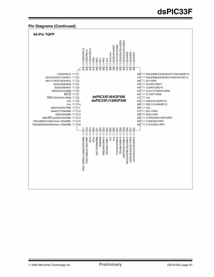
dsPIC33F
Pin Diagrams (Continued)
64-Pin TQFP
12345678910111213 36
353433
32313029282726
64 63 62 61 60 59 58 57 56
141516
17 18 19 20 21 22 23 24 25
PGC2/EMUC2/SOSCO/T1CK/CN0/RC14PGD2/EMUD2/SOSCI/T4CK/CN1/RC13OC1/RD0IC4/INT4/RD11
IC2/U1CTS/INT2/RD9IC1/INT1/RD8VSS
OSC2/CLKO/RC15OSC1/CLKIN/RC12VDD
SCL1/RG2
U1RTS/SCK1/INT0/RF6U1RX/SDI1/RF2U1TX/SDO1/RF3
COFS/RG15AN16/T2CK/T7CK/RC1AN17/T3CK/T6CK/RC2
SCK2/CN8/RG6SDI2/CN9/RG7
SDO2/CN10/RG8MCLR
VSS
VDD
AN3/CN5/RB3AN2/SS1/LVDIN/CN4/RB2
PGC3/EMUC3/AN1/VREF-/CN3/RB1PGD3/EMUD3/AN0/VREF+/CN2/RB0
OC
8/C
N16
/RD
7
CS
DO
/RG
13C
SD
I/RG
12C
SC
K/R
G14
VD
DC
OR
E
RG
1R
F1
RG
0
OC
2/R
D1
OC
3/R
D2
PG
C1/
EM
UC
1/A
N6/
OC
FA/R
B6
PG
D1/
EM
UD
1/A
N7/
RB
7A
VD
D
AV
SS
U2C
TS
/AN
8/R
B8
AN
9/R
B9
TM
S/A
N10
/RB
10T
DO
/AN
11/R
B11
VS
S
VD
D
TC
K/A
N12
/RB
12T
DI/A
N13
/RB
13U
2RT
S/A
N14
/RB
14A
N15
/OC
FB
/CN
12/R
B15
U2T
X/S
CL2
/CN
18/R
F5
U2R
X/S
DA
2/C
N17
/RF
4
SDA1/RG3
43424140393837
44
484746
50 495154 53 5255
45
SS2/T5CK/CN11/RG9
AN5/IC8/CN7/RB5AN4/IC7/CN6/RB4
IC3/INT3/RD10
VD
D
RF
0
OC
4/R
D3
OC
7/C
N15
/RD
6O
C6/
IC6/
CN
14/R
D5
OC
5/IC
5/C
N13
/RD
4
dsPIC33FJ64GP306dsPIC33FJ128GP306
© 2005 Microchip Technology Inc. Preliminary DS70155C-page 67

dsPIC33F
Pin Diagrams (Continued)
64-Pin TQFP
12345678910111213 36
353433
32313029282726
64 63 62 61 60 59 58 57 56
141516
17 18 19 20 21 22 23 24 25
PGC2/EMUC2/SOSCO/T1CK/CN0/RC14PGD2/EMUD2/SOSCI/T4CK/CN1/RC13OC1/RD0IC4/INT4/RD11
IC2/U1CTS/INT2/RD9IC1/INT1/RD8VSS
OSC2/CLKO/RC15OSC1/CLKIN/RC12VDD
SCL1/RG2
U1RTS/SCK1/INT0/RF6U1RX/SDI1/RF2U1TX/SDO1/RF3
COFS/RG15AN16/T2CK/T7CK/RC1AN17/T3CK/T6CK/RC2
SCK2/CN8/RG6SDI2/CN9/RG7
SDO2/CN10/RG8MCLR
VSS
VDD
AN3/CN5/RB3AN2/SS1/LVDIN/CN4/RB2
PGC3/EMUC3/AN1/VREF-/CN3/RB1PGD3/EMUD3/AN0/VREF+/CN2/RB0
OC
8/C
N16
/RD
7
CS
DO
/RG
13C
SD
I/RG
12C
SC
K/R
G14
VD
DC
OR
E
RG
1C
1TX
/RF
1
RG
0
OC
2/R
D1
OC
3/R
D2
PG
C1/
EM
UC
1/A
N6/
OC
FA/R
B6
PG
D1/
EM
UD
1/A
N7/
RB
7A
VD
D
AV
SS
U2C
TS
/AN
8/R
B8
AN
9/R
B9
TM
S/A
N10
/RB
10T
DO
/AN
11/R
B11
VS
S
VD
D
TC
K/A
N12
/RB
12T
DI/A
N13
/RB
13U
2RT
S/A
N14
/RB
14A
N15
/OC
FB
/CN
12/R
B15
U2T
X/S
CL2
/CN
18/R
F5
U2R
X/S
DA
2/C
N17
/RF
4
SDA1/RG3
43424140393837
44
484746
50 495154 53 5255
45
SS2/T5CK/CN11/RG9
AN5/IC8/CN7/RB5AN4/IC7/CN6/RB4
IC3/INT3/RD10
VD
D
C1R
X/R
F0
OC
4/R
D3
OC
7/C
N15
/RD
6O
C6/
IC6/
CN
14/R
D5
OC
5/IC
5/C
N13
/RD
4
dsPIC33FJ256GP506
DS70155C-page 68 Preliminary © 2005 Microchip Technology Inc.

dsPIC33F
Pin Diagrams (Continued)
64-Pin TQFP
12345678910111213 36
353433
32313029282726
64 63 62 61 60 59 58 57 56
141516
17 18 19 20 21 22 23 24 25
PGC2/EMUC2/SOSCO/T1CK/CN0/RC14PGD2/EMUD2/SOSCI/T4CK/CN1/RC13OC1/RD0IC4/INT4/RD11
IC2/U1CTS/INT2/RD9IC1/INT1/RD8VSS
OSC2/CLKO/RC15OSC1/CLKIN/RC12VDD
SCL1/RG2
U1RTS/SCK1/INT0/RF6U1RX/SDI1/RF2U1TX/SDO1/RF3
COFS/RG15AN16/T2CK/T7CK/RC1AN17/T3CK/T6CK/RC2
SCK2/CN8/RG6SDI2/CN9/RG7
SDO2/CN10/RG8MCLR
VSS
VDD
AN3/CN5/RB3AN2/SS1/LVDIN/CN4/RB2
PGC3/EMUC3/AN1/VREF-/CN3/RB1PGD3/EMUD3/AN0/VREF+/CN2/RB0
OC
8/C
N16
/RD
7
CS
DO
/RG
13C
SD
I/RG
12C
SC
K/R
G14
VD
DC
OR
E
C2T
X/R
G1
C1T
X/R
F1
C2R
X/R
G0
OC
2/R
D1
OC
3/R
D2
PG
C1/
EM
UC
1/A
N6/
OC
FA/R
B6
PG
D1/
EM
UD
1/A
N7/
RB
7A
VD
D
AV
SS
U2C
TS
/AN
8/R
B8
AN
9/R
B9
TM
S/A
N10
/RB
10T
DO
/AN
11/R
B11
VS
S
VD
D
TC
K/A
N12
/RB
12T
DI/A
N13
/RB
13U
2RT
S/A
N14
/RB
14A
N15
/OC
FB
/CN
12/R
B15
U2T
X/S
CL2
/CN
18/R
F5
U2R
X/S
DA
2/C
N17
/RF
4
SDA1/RG3
43424140393837
44
484746
50 495154 53 5255
45
SS2/T5CK/CN11/RG9
AN5/IC8/CN7/RB5AN4/IC7/CN6/RB4
IC3/INT3/RD10
VD
D
C1R
X/R
F0
OC
4/R
D3
OC
7/C
N15
/RD
6O
C6/
IC6/
CN
14/R
D5
OC
5/IC
5/C
N13
/RD
4
dsPIC33FJ64GP706dsPIC33FJ128GP706
© 2005 Microchip Technology Inc. Preliminary DS70155C-page 69

dsPIC33F
Pin Diagrams (Continued)
80-Pin TQFP
72
74
73
71
70
69
68
67
66
65
64
63
62
61
20
2
3
4
5
6
7
8
9
10
11
12
13
14
15
16
50
49
48
47
46
45
44
21
41
4039383736353423 24 25 26 27 28 29 30 31 32 33
dsPIC33FJ64GP708
17
18
19
75
1
57
56
55
54
53
52
51
60
59
58
43
42
76
78
77
79
2280
IC5/
RD
12O
C4/
RD
3
OC
3/R
D2
OC
2/R
D1
CSC
K/R
G14
AN23
/CN
23/R
A7
AN22
/CN
22/R
A6C
2RX/
RG
0
C2T
X/R
G1
C1T
X/R
F1
C1R
X/R
F0
CSD
O/R
G13
CSD
I/RG
12
OC
8/C
N16
/RD
7
OC
6/C
N14
/RD
5
OC1/RD0
IC4/RD11
IC2/RD9
IC1/RD8
IC3/RD10
VSS
OSC1/CLKIN/RC12
VDD
SCL1/RG2
U1RX/RF2
U1TX/RF3
PGC2/EMUC2/SOSCO/T1CK/CN0/RC14
PGD2/EMUD2/SOSCI/CN1/RC13
VREF
+/R
A10
VREF
-/RA9
AVD
D
AVSS
U2C
TS/A
N8/
RB8
AN9/
RB9
AN10
/RB1
0
AN11
/RB1
1
VDD
U2R
X/C
N17
/RF4
IC8/
U1R
TS/C
N21
/RD
15
U2T
X/C
N18
/RF5
PGC
1/EM
UC
1/AN
6/O
CFA
/RB6
PGD
1/EM
UD
1/AN
7/R
B7
AN17/T3CK/T6CK/RC2
AN18/T4CK/T9CK/RC3
AN19/T5CK/T8CK/RC4
SCK2/CN8/RG6
SDI2/CN9/RG7
SDO2/CN10/RG8
MCLR
SS2/CN11/RG9
AN4/CN6/RB4
AN3/CN5/RB3
AN2/SS1/LVDIN/CN4/RB2
PGC3/EMUC3/AN1/CN3/RB1
PGD3/EMUD3/AN0/CN2/RB0
VSS
VDD
COFS/RG15
AN16/T2CK/T7CK/RC1
TDO/AN21/INT2/RE9
TMS/AN20/INT1/RE8
TCK/
AN12
/RB1
2
TDI/A
N13
/RB1
3
U2R
TS/A
N14
/RB1
4
AN15
/OC
FB/C
N12
/RB1
5
VDD
VDD
CO
RE
OC
5/C
N13
/RD
4
IC6/
CN
19/R
D13
SDA1/RG3
SDI1/RF7
SDO1/RF8
AN5/CN7/RB5
VSS
OSC2/CLKO/RC15
OC
7/C
N15
/RD
6
SCK1/INT0/RF6
IC7/
U1C
TS/C
N20
/RD
14
SDA2/INT4/RA15
SCL2/INT3/RA14
dsPIC33FJ128GP708
DS70155C-page 70 Preliminary © 2005 Microchip Technology Inc.

dsPIC33F
Pin Diagrams (Continued)
9294 93 91 90 89 88 87 86 85 84 83 82 81 80 79 78
20
2
3
4
5
6
7
8
9
10
11
12
13
14
15
16
65
64
63
62
61
60
59
26
56
4544434241403928 29 30 31 32 33 34 35 36 37 38
17
18
19
21
22
95
1
7677
72
71
70
69
68
67
66
75
74
73
58
57
2423
25
9698 979927 46 47 48 49 50
55
54
53
52
51
OC
6/C
N14
/RD
5O
C5/
CN
13/R
D4
IC6/
CN
19/R
D13
IC5/
RD
12O
C4/
RD
3O
C3/
RD
2O
C2/
RD
1
AN23
/CN
23/R
A7AN
22/C
N22
/RA6
AN26
/RE2
CSD
O/R
G13
CSD
I/RG
12C
SCK/
RG
14AN
25/R
E1AN
24/R
E0
RG
0
AN28
/RE4
AN27
/RE3
RF0
VDD
CO
RE
PGD2/EMUD2/SOSCI/CN1/RC13
OC1/RD0
IC3/RD10
IC2/RD9
IC1/RD8
IC4/RD11
SDA2/RA3
SCL2/RA2
OSC2/CLKO/RC15
OSC1/CLKIN/RC12
VDD
SCL1/RG2
SCK1/INT0/RF6
SDI1/RF7
SDO1/RF8
SDA1/RG3
U1RX/RF2
U1TX/RF3
VSS
PGC2/EMUC2/SOSCO/T1CK/CN0/RC14VR
EF+/
RA1
0VR
EF-/R
A9
AVD
D
AVSS
AN8/
RB8
AN9/
RB9
AN10
/RB1
0AN
11/R
B11
V DD
U2C
TS/R
F12
U2R
TS/R
F13
IC7/
U1C
TS/C
N20
/RD
14IC
8/U
1RTS
/CN
21/R
D15
V DD
VSS
PGC
1/EM
UC
1/AN
6/O
CFA
/RB6
PGD
1/EM
UD
1/AN
7/R
B7
U2T
X/C
N18
/RF5
U2R
X/C
N17
/RF4
AN29/RE5
AN30/RE6
AN31/RE7AN16/T2CK/T7CK/RC1
AN17/T3CK/T6CK/RC2
AN18/T4CK/T9CK/RC3AN19/T5CK/T8CK/RC4
SCK2/CN8/RG6
VDD
TMS/RA0
AN20/INT1/RE8
AN21/INT2/RE9
AN5/CN7/RB5AN4/CN6/RB4
AN3/CN5/RB3AN2/SS1/LVDIN/CN4/RB2
SDI2/CN9/RG7
SDO2/CN10/RG8
PGC3/EMUC3/AN1/CN3/RB1
PGD3/EMUD3/AN0/CN2/RB0
COFS/RG15
VDD
SS2/CN11/RG9
MCLR
AN12
/RB1
2AN
13/R
B13
AN14
/RB1
4AN
15/O
CFB
/CN
12/R
B15
RG
1R
F1
OC
8/C
N16
/RD
7O
C7/
CN
15/R
D6
TDO/RA5
INT4/RA15
INT3/RA14
VSS
VSS
VSSVD
D
TDI/RA4
TCK/
RA1
100-Pin TQFP
dsPIC33FJ64GP310dsPIC33FJ128GP310
100
© 2005 Microchip Technology Inc. Preliminary DS70155C-page 71

dsPIC33F
Pin Diagrams (Continued)
9294 93 91 90 89 88 87 86 85 84 83 82 81 80 79 78
20
2
3
4
5
6
7
8
9
10
11
12
13
14
15
16
65
64
63
62
61
60
59
26
56
4544434241403928 29 30 31 32 33 34 35 36 37 38
17
18
19
21
22
951
7677
72
71
70
69
68
67
66
75
74
73
58
57
24
23
25
9698 979927 46 47 48 49 50
55
54
53
52
51
OC
6/C
N14
/RD
5O
C5/
CN
13/R
D4
IC6/
CN
19/R
D13
IC5/
RD
12O
C4/
RD
3O
C3/
RD
2O
C2/
RD
1
AN
23/C
N23
/RA
7A
N22
/CN
22/R
A6
AN
26/R
E2
CS
DO
/RG
13C
SD
I/RG
12C
SC
K/R
G14
AN
25/R
E1
AN
24/R
E0
RG
0
AN
28/R
E4
AN
27/R
E3
C1R
X/R
F0
VD
DC
OR
E
PGD2/EMUD2/SOSCI/CN1/RC13
OC1/RD0
IC3/RD10
IC2/RD9
IC1/RD8
IC4/RD11
SDA2/RA3
SCL2/RA2
OSC2/CLKO/RC15
OSC1/CLKIN/RC12
VDD
SCL1/RG2
SCK1/INT0/RF6
SDI1/RF7
SDO1/RF8
SDA1/RG3
U1RX/RF2
U1TX/RF3
VSS
PGC2/EMUC2/SOSCO/T1CK/CN0/RC14
VREF
+/R
A10
VREF
-/RA9
AVD
D
AVSS
AN8/
RB8
AN9/
RB9
AN10
/RB1
0AN
11/R
B11
V DD
U2C
TS/R
F12
U2R
TS/R
F13
IC7/
U1C
TS/C
N20
/RD
14IC
8/U
1RTS
/CN
21/R
D15
V DD
VSS
PGC
1/EM
UC
1/AN
6/O
CFA
/RB6
PGD
1/EM
UD
1/AN
7/R
B7
U2T
X/C
N18
/RF5
U2R
X/C
N17
/RF4
AN29/RE5
AN30/RE6
AN31/RE7
AN16/T2CK/T7CK/RC1
AN17/T3CK/T6CK/RC2
AN18/T4CK/T9CK/RC3AN19/T5CK/T8CK/RC4
SCK2/CN8/RG6
VDD
TMS/RA0
AN20/INT1/RE8
AN21/INT2/RE9
AN5/CN7/RB5
AN4/CN6/RB4
AN3/CN5/RB3AN2/SS1/LVDIN/CN4/RB2
SDI2/CN9/RG7
SDO2/CN10/RG8
PGC3/EMUC3/AN1/CN3/RB1
PGD3/EMUD3/AN0/CN2/RB0
COFS/RG15
VDD
SS2/CN11/RG9
MCLR
AN12
/RB1
2AN
13/R
B13
AN14
/RB1
4AN
15/O
CFB
/CN
12/R
B15
RG
1C
1TX
/RF
1
OC
8/C
N16
/RD
7O
C7/
CN
15/R
D6
TDO/RA5
INT4/RA15
INT3/RA14
VSS
VSS
VSS
VD
D
TDI/RA4
TCK/
RA1
100-Pin TQFP
dsPIC33FJ256GP510
100
DS70155C-page 72 Preliminary © 2005 Microchip Technology Inc.
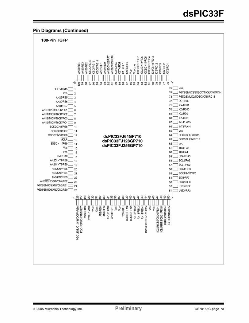
dsPIC33F
Pin Diagrams (Continued)
9294 93 91 90 89 88 87 86 85 84 83 82 81 80 79 78
20
2
3
4
5
6
7
8
9
10
11
12
13
14
15
16
65
64
63
62
61
60
59
26
56
4544434241403928 29 30 31 32 33 34 35 36 37 38
17
18
19
21
22
95
1
7677
72
71
70
69
68
67
66
75
74
73
58
57
24
23
25
9698 979927 46 47 48 49 50
55
54
53
52
51
OC
6/C
N14
/RD
5O
C5/
CN
13/R
D4
IC6/
CN
19/R
D13
IC5/
RD
12O
C4/
RD
3O
C3/
RD
2O
C2/
RD
1
AN23
/CN
23/R
A7AN
22/C
N22
/RA6
AN26
/RE2
CSD
O/R
G13
CSD
I/RG
12C
SCK/
RG
14AN
25/R
E1AN
24/R
E0
C2R
X/R
G0
AN28
/RE4
AN27
/RE3
C1R
X/R
F0
VDD
CO
RE
PGD2/EMUD2/SOSCI/CN1/RC13
OC1/RD0
IC3/RD10
IC2/RD9
IC1/RD8
IC4/RD11
SDA2/RA3
SCL2/RA2
OSC2/CLKO/RC15
OSC1/CLKIN/RC12
VDD
SCL1/RG2
SCK1/INT0/RF6
SDI1/RF7
SDO1/RF8
SDA1/RG3
U1RX/RF2
U1TX/RF3
VSS
PGC2/EMUC2/SOSCO/T1CK/CN0/RC14VR
EF+
/RA1
0VR
EF-
/RA9
AVD
D
AVSS
AN8/
RB8
AN9/
RB9
AN10
/RB1
0AN
11/R
B11
V DD
U2C
TS/R
F12
U2R
TS/R
F13
IC7/
U1C
TS/C
N20
/RD
14IC
8/U
1RTS
/CN
21/R
D15
V DD
VSS
PGC
1/EM
UC
1/AN
6/O
CFA
/RB6
PGD
1/EM
UD
1/AN
7/R
B7
U2T
X/C
N18
/RF5
U2R
X/C
N17
/RF4
AN29/RE5
AN30/RE6
AN31/RE7AN16/T2CK/T7CK/RC1
AN17/T3CK/T6CK/RC2
AN18/T4CK/T9CK/RC3
AN19/T5CK/T8CK/RC4
SCK2/CN8/RG6
VDD
TMS/RA0
AN20/INT1/RE8AN21/INT2/RE9
AN5/CN7/RB5AN4/CN6/RB4
AN3/CN5/RB3AN2/SS1/LVDIN/CN4/RB2
SDI2/CN9/RG7
SDO2/CN10/RG8
PGC3/EMUC3/AN1/CN3/RB1
PGD3/EMUD3/AN0/CN2/RB0
COFS/RG15
VDD
SS2/CN11/RG9MCLR
AN12
/RB1
2AN
13/R
B13
AN14
/RB1
4AN
15/O
CFB
/CN
12/R
B15
C2T
X/R
G1
C1T
X/R
F1
OC
8/C
N16
/RD
7O
C7/
CN
15/R
D6
TDO/RA5
INT4/RA15
INT3/RA14
VSS
VSS
VSSVD
D
TDI/RA4
TCK/
RA1
100-Pin TQFP
dsPIC33FJ128GP710
100
dsPIC33FJ256GP710
dsPIC33FJ64GP710
© 2005 Microchip Technology Inc. Preliminary DS70155C-page 73

dsPIC33F
APPENDIX B: DEVICE I/O PINOUTS AND FUNCTIONS FOR MOTOR CONTROL FAMILY
Table B-1 provides a brief description of device I/Opinouts and the functions that may be multiplexed to aport pin. Multiple functions may exist on one port pin.When multiplexing occurs, the peripheral module’sfunctional requirements may force an override of thedata direction of the port pin.
TABLE B-1: PINOUT I/O DESCRIPTIONS FOR MOTOR CONTROL FAMILY
Pin NamePin
TypeBufferType
Description
AN0-AN23 I Analog Analog input channels. AN0 and AN1 are also used for device programming data and clock inputs, respectively.
AVDD P P Positive supply for analog module.
AVSS P P Ground reference for analog module.
CLKICLKO
IO
ST/CMOS—
External clock source input. Always associated with OSC1 pin function.Oscillator crystal output. Connects to crystal or resonator in Crystal Oscillator mode. Optionally functions as CLKO in RC and EC modes. Always associated with OSC2 pin function.
CN0-CN23 I ST Input change notification inputs.Can be software programmed for internal weak pull-ups on all inputs.
COFSCSCKCSDICSDO
I/OI/OIO
STSTST—
Data Converter Interface frame synchronization pin.Data Converter Interface serial clock input/output pin.Data Converter Interface serial data input pin.Data Converter Interface serial data output pin.
C1RXC1TXC2RXC2TX
IOIO
ST—ST—
CAN1 bus receive pin.CAN1 bus transmit pin.CAN2 bus receive pin.CAN2 bus transmit pin.
PGD1/EMUD1PGC1/EMUC1PGD2/EMUD2PGC2/EMUC2PGD3/EMUD3PGC3/EMUC3
I/OI
I/OI
I/OI
STSTSTSTSTST
Data I/O pin for programming/debugging communication channel 1.Clock input pin for programming/debugging communication channel 1.Data I/O pin for programming/debugging communication channel 2.Clock input pin for programming/debugging communication channel 2.Data I/O pin for programming/debugging communication channel 3.Clock input pin for programming/debugging communication channel 3.
IC1-IC8 I ST Capture inputs 1 through 8.
INDXQEA
QEB
UPDN
II
I
O
STST
ST
CMOS
Quadrature Encoder Index Pulse input.Quadrature Encoder Phase A input in QEI mode. Auxiliary Timer External Clock/Gate input in Timer mode.Quadrature Encoder Phase A input in QEI mode. Auxiliary Timer External Clock/Gate input in Timer mode.Position Up/Down Counter Direction State.
INT0INT1INT2INT3INT4
IIIII
STSTSTSTST
External interrupt 0.External interrupt 1.External interrupt 2.External interrupt 3.External interrupt 4.
FLTAFLTBPWM1LPWM1HPWM2LPWM2HPWM3LPWM3HPWM4LPWM4H
IIOOOOOOOO
STST————————
PWM Fault A input.PWM Fault B input.PWM 1 low output. PWM 1 high output.PWM 2 low output.PWM 2 high output.PWM 3 low output.PWM 3 high output.PWM 4 low output.PWM 4 high output.
Legend: CMOS = CMOS compatible input or output; Analog = Analog inputST = Schmitt Trigger input with CMOS levels; O = Output; I = Input; P = Power
DS70155C-page 74 Preliminary © 2005 Microchip Technology Inc.

dsPIC33F
MCLR I/P ST Master Clear (Reset) input or programming voltage input. This pin is an active-low Reset to the device.
OCFAOCFBOC1-OC8
IIO
STST—
Compare Fault A input (for Compare Channels 1, 2, 3 and 4).Compare Fault B input (for Compare Channels 5, 6, 7 and 8).Compare outputs 1 through 8.
OSC1OSC2
II/O
ST/CMOS—
Oscillator crystal input. ST buffer when configured in RC mode; CMOS otherwise.Oscillator crystal output. Connects to crystal or resonator in Crystal Oscillator mode. Optionally functions as CLKO in RC and EC modes.
RA0-RA7RA9-RA10RA12-RA15
I/OI/OI/O
STSTST
PORTA is a bidirectional I/O port.
RB0-RB15 I/O ST PORTB is a bidirectional I/O port.
RC1-RC4RC12-RC15
I/OI/O
STST
PORTC is a bidirectional I/O port.
RD0-RD15 I/O ST PORTD is a bidirectional I/O port.
RE0-RE9 I/O ST PORTE is a bidirectional I/O port.
RF0-RF8 RF12-RF13
I/O ST PORTF is a bidirectional I/O port.
RG0-RG3RG6-RG9RG12-RG15
I/OI/OI/O
STSTST
PORTG is a bidirectional I/O port.
SCK1SDI1SDO1SS1SCK2SDI2SDO2SS2
I/OIOI
I/OIOI
STST—STSTST—ST
Synchronous serial clock input/output for SPI1.SPI1 data in.SPI1 data out.SPI1 slave synchronization.Synchronous serial clock input/output for SPI2.SPI2 data in.SPI2 data out.SPI2 slave synchronization.
SCL1SDA1SCL2SDA2
I/OI/OI/OI/O
STSTSTST
Synchronous serial clock input/output for I2C1.Synchronous serial data input/output for I2C1.Synchronous serial clock input/output for I2C2.Synchronous serial data input/output for I2C2.
SOSCISOSCO
IO
ST/CMOS—
32 kHz low-power oscillator crystal input; CMOS otherwise.32 kHz low-power oscillator crystal output.
TMSTCKTDITDO
II/OIO
STSTST—
JTAG Test mode select pin.JTAG test clock input/output pin.JTAG test data input pin.JTAG test data output pin.
T1CKT2CKT3CKT4CKT5CKT6CKT7CKT8CKT9CK
IIIIIIIII
STSTSTSTSTSTSTSTST
Timer1 external clock input.Timer2 external clock input.Timer3 external clock input.Timer4 external clock input.Timer5 external clock input.Timer6 external clock input.Timer7 external clock input.Timer8 external clock input.Timer9 external clock input.
TABLE B-1: PINOUT I/O DESCRIPTIONS FOR MOTOR CONTROL FAMILY (CONTINUED)
Pin NamePin
TypeBufferType
Description
Legend: CMOS = CMOS compatible input or output; Analog = Analog inputST = Schmitt Trigger input with CMOS levels; O = Output; I = Input; P = Power
© 2005 Microchip Technology Inc. Preliminary DS70155C-page 75

dsPIC33F
TABLE B-2: dsPIC33F MOTOR CONTROL FAMILY VARIANTS (DEVICES MARKED “PS”)
U1CTSU1RTSU1RXU1TXU2CTSU2RTSU2RXU2TX
IOIOIOIO
ST—ST—ST—ST—
UART1 clear to send.UART1 ready to send.UART1 receive.UART1 transmit.UART2 clear to send.UART2 ready to send.UART2 receive.UART2 transmit.
VDD P — Positive supply for peripheral logic and I/O pins.
VDDCORE P — CPU logic filter capacitor connection.
VSS P — Ground reference for logic and I/O pins.
VREF+ I Analog Analog voltage reference (high) input.
VREF- I Analog Analog voltage reference (low) input.
TABLE B-1: PINOUT I/O DESCRIPTIONS FOR MOTOR CONTROL FAMILY (CONTINUED)
Pin NamePin
TypeBufferType
Description
Legend: CMOS = CMOS compatible input or output; Analog = Analog inputST = Schmitt Trigger input with CMOS levels; O = Output; I = Input; P = Power
Device Pins
Program Flash
Memory(KB)
RAM(KB)(1)
Tim
er 1
6-b
it
Inp
ut
Cap
ture
Ou
tpu
t C
om
pare
Std
. PW
M
Mo
tor
Co
ntr
ol P
WM
Qu
adra
ture
En
cod
erIn
terf
ace
Co
dec
Inte
rfac
e
A/D
Co
nve
rter
UA
RT
SP
I™
I2 C™
CA
N
I/O P
ins
(Max
)(2)
Packages
33FJ128MC706 64 128 17 9 8 8 8 ch 1 0 2 A/D, 16 ch
2 2 2 1 53 PT
33FJ128MC708 80 128 17 9 8 8 8 ch 1 0 2 A/D, 18 ch
2 2 2 1 69 PT
33FJ256MC710 100 256 33 9 8 8 8 ch 1 0 2 A/D, 24 ch
2 2 2 2 86 PF
Note 1: RAM size is inclusive of 1 KB DMA RAM.2: Maximum I/O pin count includes pins shared by the peripheral functions.
Note: Prototype samples are intended for dsPIC33F early adopters and are based on early revision silicon. Devicesare marked with “PS” suffix. Major differences are noted in this data sheet. For additional information, pleaserefer to the “dsPIC33F Data Sheet”.
DS70155C-page 76 Preliminary © 2005 Microchip Technology Inc.

dsPIC33F
Pin Diagrams
64-Pin TQFP
12345678910111213 36
353433
32313029282726
64 63 62 61 60 59 58 57 56
141516
17 18 19 20 21 22 23 24 25
EMUC1/SOSCO/T1CK/CN0/RC14EMUD1/SOSCI/T4CK/CN1/RC13EMUC2/OC1/RD0IC4/INT4/RD11
IC2/FLTB/INT2/RD9IC1/FLTA/INT1/RD8VSS
OSC2/CLKO/RC15OSC1/CLKIN/RC12VDD
SCL1/RG2
EMUC3/SCK1/INT0/RF6U1RX/SDI1/RF2EMUD3/U1TX/SDO1/RF3
PWM3H/RE5PWM4L/RE6PWM4H/RE7
SCK2/CN8/RG6SDI2/CN9/RG7
SDO2/CN10/RG8MCLR
VSS
VDD
AN3/INDX/CN5/RB3AN2/SS1/LVDIN/CN4/RB2
AN1/VREF-/CN3/RB1AN0/VREF+/CN2/RB0
OC
8/U
PD
N/C
N16
/RD
7
PW
M3L
/RE
4P
WM
2H/R
E3
PW
M2L
/RE
2
VD
DC
OR
E
PW
M1L
/RE
0C
1TX
/RF
1
PW
M1H
/RE
1
EM
UD
2/O
C2/
RD
1O
C3/
RD
2
PG
C/E
MU
C/A
N6/
OC
FA/R
B6
PG
D/E
MU
D/A
N7/
RB
7A
VD
D
AV
SS
AN
8/R
B8
AN
9/R
B9
AN
10/R
B10
AN
11/R
B11
VS
S
VD
D
AN
12/R
B12
AN
13/R
B13
AN
14/R
B14
AN
15/O
CF
B/C
N12
/RB
15
U2T
X/S
CL2
/CN
18/R
F5
U2R
X/S
DA
2/C
N17
/RF
4SDA1/RG3
43424140393837
44
484746
50 495154 53 5255
45
SS2/T5CK/CN11/RG9
AN5/QEB/IC8/CN7/RB5AN4/QEA/IC7/CN6/RB4
IC3/INT3/RD10
VD
D
C1R
X/R
F0
OC
4/R
D3
OC
7/C
N15
/RD
6O
C6/
IC6/
CN
14/R
D5
OC
5/IC
5/C
N13
/RD
4
dsPIC33FJ128MC706*
*Device is marked with ‘PS’ designator.
© 2005 Microchip Technology Inc. Preliminary DS70155C-page 77

dsPIC33F
Pin Diagrams (Continued)
80-Pin TQFP
72
74 73
71 70 69 68 67 66 65 64 63 62 61
20
2
3
4
5
6
7
8
9
10
11
12
13
14
15
16
50
49
48
47
46
45
44
21
41
4039383736353423 24 25 26 27 28 29 30 31 32 33
17
18
19
751
57
56
55
54
53
52
51
60
59
58
43
42
7678 777922
80
IC5/
RD
12
OC
4/R
D3
OC
3/R
D2
EM
UD
2/O
C2/
RD
1
PW
M2L
/RE
2P
WM
1H/R
E1
PW
M1L
/RE
0
CR
X2/
RG
0
C2T
X/R
G1
C1T
X/R
F1
C1R
X/R
F0
PW
M3L
/RE
4
PW
M2H
/RE
3
OC
8/C
N16
/UP
DN
/RD
7
OC
6/C
N14
/RD
5
EMUC2/OC1/RD0
IC4/RD11
IC2/RD9
IC1/RD8
IC3/RD10
VSS
OSC1/CLKIN/RC12
VDD
SCL1/RG2
U1RX/RF2
EMUD3/U1TX/RF3
EMUC1/SOSCO/T1CK/CN0/RC14
EMUD1/SOSCI/CN1/RC13
VR
EF+/
RA
10
VR
EF-/
RA
9
AVD
D
AVS
S
AN
8/R
B8
AN
9/R
B9
AN
10/R
B10
AN
11/R
B11
VD
D
U2R
X/C
N17
/RF
4
IC8/
CN
21/R
D15
U2T
X/C
N18
/RF
5
AN
6/O
CFA
/RB
6
AN
7/R
B7
PWM4H/RE7
AN16/T2CK/T7CK/RC1
AN17/T3CK/T6CK/RC2
SCK2/CN8/RG6
SDI2/CN9/RG7
SDO2/CN10/RG8
MCLR
SS2/CN11/RG9
AN4/QEA/CN6/RB4
AN3/INDX/CN5/RB3
AN2/SS1/LVDIN/CN4/RB2
PGC/EMUC/AN1/CN3/RB1
PGD/EMUD/AN0/CN2/RB0
VSS
VDD
PWM3H/RE5
PWM4L/RE6
FLTB/INT2/RE9
FLTA/INT1/RE8
AN
12/R
B12
AN
13/R
B13
AN
14/R
B14
AN
15/O
CFB
/CN
12/R
B15
VD
D
VD
DC
OR
E
OC
5/C
N13
/RD
4
IC6/
CN
19/R
D13
SDA1/RG3
SDI1/RF7
SDO1/RF8
AN5/QEB/CN7/RB5
VS
S
OSC2/CLKO/RC15
OC
7/C
N15
/RD
6
EMUC3/SCK1/INT0/RF6
IC7/
CN
20/R
D14
SDA2/INT4/RA15
SCL2/INT3/RA14
dsPIC33FJ128MC708*
*Device is marked with ‘PS’ designator.
DS70155C-page 78 Preliminary © 2005 Microchip Technology Inc.

dsPIC33F
Pin Diagrams (Continued)
92
94
93
91
90
89
88
87
86
85
84
83
82
81
80
79
78
20
2
34
5
6
7
8
9
10
11
1213
14
15
16
65
64
63
62
61
60
59
26
56
4544434241403928 29 30 31 32 33 34 35 36 37 38
17
18
19
21
22
95
1
76
77
72
71
70
69
68
67
66
75
74
73
58
57
24
23
25
96
98
97
99
27 46 47 48 49 50
55
54
53
52
51
100
OC
6/C
N14
/RD
5O
C5/
CN
13/R
D4
IC6/
CN
19/R
D13
IC5/
RD
12O
C4/
RD
3O
C3/
RD
2E
MU
D2/
OC
2/R
D1
AN
23/C
N23
/RA
7A
N22
/CN
22/R
A6
PW
M2L
/RE
2C
SD
O/R
G13
CS
DI/R
G12
CS
CK
/RG
14P
WM
1H/R
E1
PW
M1L
/RE
0
C2R
X/R
G0
PW
M3L
/RE
4P
WM
2H/R
E3
C1R
X/R
F0
VD
DC
OR
E
EMUD1/SOSCI/CN1/RC13
EMUC2/OC1/RD0
IC3/RD10
IC2/RD9
IC1/RD8
IC4/RD11
SDA2/RA3
SCL2/RA2
OSC2/CLKO/RC15
OSC1/CLKIN/RC12
VDD
SCL1/RG2
EMUC3/SCK1/INT0/RF6
SDI1/RF7
SDO1/RF8
SDA1/RG3
U1RX/RF2
EMUD3/U1TX/RF3
VSS
EMUC1/SOSCO/T1CK/CN0/RC14
VRE
F+/R
A10
VRE
F-/R
A9
AVD
D
AVS
S
AN
8/R
B8
AN
9/R
B9
AN
10/R
B10
AN
11/R
B11
VD
D
U2C
TS/R
F12
U2R
TS/R
F13
IC7/
CN
20/R
D14
IC8/
CN
21/R
D15
VD
D
VS
S
AN
6/O
CFA
/RB
6A
N7/
RB
7
U2T
X/C
N18
/RF5
U2R
X/C
N17
/RF4
PWM3H/RE5
PWM4L/RE6PWM4H/RE7
AN16/T2CK/T7CK/RC1
AN17/T3CK/T6CK/RC2
AN18/T4CK/T9CK/RC3
AN19/T5CK/T8CK/RC4
SCK2/CN8/RG6
VDD
RA0
AN20/FLTA/INT1/RA12
AN21/FLTB/INT2/RA13
AN5/QEB/CN7/RB5AN4/QEA/CN6/RB4
AN3/INDX/CN5/RB3AN2/SS1/LVDIN/CN4/RB2
SDI2/CN9/RG7
SDO2/CN10/RG8
PGC/EMUC/AN1/CN3/RB1
PGD/EMUD/AN0/CN2/RB0
COFS/RG15
VDD
SS2/CN11/RG9
MCLR
AN
12/R
B12
AN
13/R
B13
AN
14/R
B14
AN
15/O
CFB
/CN
12/R
B15
C2T
X/R
G1
C1T
X/R
F1
OC
8/U
PD
N//C
N16
/RD
7O
C7/
CN
15/R
D6
RA5
INT4/RA15
INT3/RA14
VSS
VS
S
VSS
VD
D
RA4
RA
1
100-Pin TQFP
dsPIC33FJ256MC710*
*Device is marked with ‘PS’ designator.
© 2005 Microchip Technology Inc. Preliminary DS70155C-page 79

dsPIC33F
Pin Diagrams (Continued)
64-Pin TQFP
12345678910111213 36
353433
32313029282726
64 63 62 61 60 59 58 57 56
141516
17 18 19 20 21 22 23 24 25
PGC2/EMUC2/SOSCO/T1CK/CN0/RC14PGD2/EMUD2/SOSCI/T4CK/CN1/RC13OC1/RD0IC4/INT4/RD11
IC2/U1CTS/FLTB/INT2/RD9IC1/FLTA/INT1/RD8VSS
OSC2/CLKO/RC15OSC1/CLKIN/RC12VDD
SCL1/RG2
U1RTS/SCK1/INT0/RF6U1RX/SDI1/RF2U1TX/SDO1/RF3
PWM3H/RE5PWM4L/RE6PWM4H/RE7
SCK2/CN8/RG6SDI2/CN9/RG7
SDO2/CN10/RG8MCLR
VSS
VDD
AN3/INDX/CN5/RB3AN2/SS1/LVDIN/CN4/RB2
PGC3/EMUC3/AN1/VREF-/CN3/RB1PGD3/EMUD3/AN0/VREF+/CN2/RB0
OC
8/U
PD
N/C
N16
/RD
7
PW
M3L
/RE
4P
WM
2H/R
E3
PW
M2L
/RE
2
VD
DC
OR
E
PW
M1L
/RE
0C
1TX
/RF1
PW
M1H
/RE
1
OC
2/R
D1
OC
3/R
D2
PG
C1/
EM
UC
1/A
N6/
OC
FA/R
B6
PG
D1/
EM
UD
1/A
N7/
RB
7AV
DD
AVS
S
U2C
TS
/AN
8/R
B8
AN
9/R
B9
TM
S/A
N10
/RB
10T
DO
/AN
11/R
B11
VS
S
VD
D
TC
K/A
N12
/RB
12T
DI/A
N13
/RB
13U
2RT
S/A
N14
/RB
14A
N15
/OC
FB
/CN
12/R
B15
U2T
X/C
N18
/RF
5U
2RX
/CN
17/R
F4
SDA1/RG3
43424140393837
44
484746
50 495154 53 5255
45
SS2/T5CK/CN11/RG9
AN5/QEB/IC8/CN7/RB5AN4/QEA/IC7/CN6/RB4
IC3/INT3/RD10
VD
D
C1R
X/R
F0
OC
4/R
D3
OC
7/C
N15
/RD
6O
C6/
IC6/
CN
14/R
D5
OC
5/IC
5/C
N13
/RD
4
dsPIC33FJ64MC506
DS70155C-page 80 Preliminary © 2005 Microchip Technology Inc.

dsPIC33F
Pin Diagrams (Continued)
64-Pin TQFP
12345678910111213 36
353433
32313029282726
64 63 62 61 60 59 58 57 56
141516
17 18 19 20 21 22 23 24 25
PGC2/EMUC2/SOSCO/T1CK/CN0/RC14PGD2/EMUD2/SOSCI/T4CK/CN1/RC13OC1/RD0IC4/INT4/RD11
IC2/U1CTS/FLTB/INT2/RD9IC1/FLTA/INT1/RD8VSS
OSC2/CLKO/RC15OSC1/CLKIN/RC12VDD
SCL1/RG2
U1RTS/SCK1/INT0/RF6U1RX/SDI1/RF2U1TX/SDO1/RF3
PWM3H/RE5PWM4L/RE6PWM4H/RE7
SCK2/CN8/RG6SDI2/CN9/RG7
SDO2/CN10/RG8MCLR
VSS
VDD
AN3/INDX/CN5/RB3AN2/SS1/LVDIN/CN4/RB2
PGC3/EMUC3/AN1/VREF-/CN3/RB1PGD3/EMUD3/AN0/VREF+/CN2/RB0
OC
8/U
PD
N/C
N16
/RD
7
PW
M3L
/RE
4P
WM
2H/R
E3
PW
M2L
/RE
2
VD
DC
OR
E
PW
M1L
/RE
0C
1TX
/RF
1
PW
M1H
/RE
1
OC
2/R
D1
OC
3/R
D2
PG
C1/
EM
UC
1/A
N6/
OC
FA/R
B6
PG
D1/
EM
UD
1/A
N7/
RB
7AV
DD
AVS
S
U2C
TS
/AN
8/R
B8
AN
9/R
B9
TM
S/A
N10
/RB
10T
DO
/AN
11/R
B11
VS
S
VD
D
TC
K/A
N12
/RB
12TD
I/AN
13/R
B13
U2R
TS
/AN
14/R
B14
AN
15/O
CF
B/C
N12
/RB
15
U2T
X/S
CL2
/CN
18/R
F5U
2RX
/SD
A2/
CN
17/R
F4
SDA1/RG3
43424140393837
44
484746
50 495154 53 5255
45
SS2/T5CK/CN11/RG9
AN5/QEB/IC8/CN7/RB5AN4/QEA/IC7/CN6/RB4
IC3/INT3/RD10
VD
D
C1R
X/R
F0
OC
4/R
D3
OC
7/C
N15
/RD
6O
C6/
IC6/
CN
14/R
D5
OC
5/IC
5/C
N13
/RD
4
dsPIC33FJ128MC506dsPIC33FJ64MC506dsPIC33FJ128MC706
© 2005 Microchip Technology Inc. Preliminary DS70155C-page 81

dsPIC33F
Pin Diagrams (Continued)
80-Pin TQFP
72
74
73
71
70
69
68
67
66
65
64
63
62
61
20
2
3
4
5
6
7
8
9
10
11
12
13
14
15
16
50
49
48
47
46
45
44
21
41
4039383736353423 24 25 26 27 28 29 30 31 32 33
17
18
19
75
1
57
56
55
54
53
52
51
60
59
58
43
42
76
78
77
79
2280
IC5/
RD
12
OC
4/R
D3
OC
3/R
D2
OC
2/R
D1
PWM
2L/R
E2PW
M1H
/RE1
PWM
1L/R
E0
CR
X2/R
G0
C2T
X/R
G1
C1T
X/R
F1
C1R
X/R
F0
PWM
3L/R
E4
PWM
2H/R
E3
OC
8/C
N16
/UPD
N/R
D7
OC
6/C
N14
/RD
5
OC1/RD0
IC4/RD11
IC2/RD9
IC1/RD8
IC3/RD10
VSS
OSC1/CLKIN/RC12
VDD
SCL1/RG2
U1RX/RF2
U1TX/RF3
PGC2/EMUC2/SOSCO/T1CK/CN0/RC14
PGD2/EMUD2/SOSCI/CN1/RC13
VREF
+/R
A10
VREF
-/RA9
AVD
D
AVS
S
U2C
TS/A
N8/
RB8
AN9/
RB9
AN10
/RB1
0
AN11
/RB1
1
VDD
U2R
X/C
N17
/RF4
IC8/
U1R
TS/C
N21
/RD
15
U2T
X/C
N18
/RF5
PGC
1/EM
UC
1/AN
6/O
CFA
/RB6
PGD
1/EM
UD
1/AN
7/R
B7
PWM4H/RE7
AN16/T2CK/T7CK/RC1
AN17/T3CK/T6CK/RC2
SCK2/CN8/RG6
SDI2/CN9/RG7
SDO2/CN10/RG8
MCLR
SS2/CN11/RG9
AN4/QEA/CN6/RB4
AN3/INDX/CN5/RB3
AN2/SS1/LVDIN/CN4/RB2
PGC3/EMUC3/AN1/CN3/RB1
PGD3/EMUD3/AN0/CN2/RB0
VSS
VDD
PWM3H/RE5
PWM4L/RE6
TDO/FLTB/INT2/RE9
TMS/FLTA/INT1/RE8
TCK/
AN12
/RB1
2
TDI/A
N13
/RB1
3
U2R
TS/A
N14
/RB1
4
AN15
/OC
FB/C
N12
/RB1
5
V DD
VDD
CO
RE
OC
5/C
N13
/RD
4
IC6/
CN
19/R
D13
SDA1/RG3
SDI1/RF7
SDO1/RF8
AN5/QEB/CN7/RB5
VSS
OSC2/CLKO/RC15
OC
7/C
N15
/RD
6
SCK1/INT0/RF6
IC7/
U1C
TS/C
N20
/RD
14
INT4/RA15
INT3/RA14
dsPIC33FJ64MC508
DS70155C-page 82 Preliminary © 2005 Microchip Technology Inc.

dsPIC33F
Pin Diagrams (Continued)
80-Pin TQFP
72
74
73
71
70
69
68
67
66
65
64
63
62
61
20
2
3
4
5
6
7
8
9
10
11
12
13
14
15
16
50
49
48
47
46
45
44
21
41
4039383736353423 24 25 26 27 28 29 30 31 32 33
17
18
19
75
1
57
56
55
54
53
52
51
60
59
58
43
42
76
78
77
79
2280
IC5/
RD
12
OC
4/R
D3
OC
3/R
D2
OC
2/R
D1
PWM
2L/R
E2PW
M1H
/RE1
PWM
1L/R
E0
CR
X2/R
G0
C2T
X/R
G1
C1T
X/R
F1
C1R
X/R
F0
PWM
3L/R
E4
PWM
2H/R
E3
OC
8/C
N16
/UPD
N/R
D7
OC
6/C
N14
/RD
5
OC1/RD0
IC4/RD11
IC2/RD9
IC1/RD8
IC3/RD10
VSS
OSC1/CLKIN/RC12
VDD
SCL1/RG2
U1RX/RF2
U1TX/RF3
PGC2/EMUC2/SOSCO/T1CK/CN0/RC14
PGD2/EMUD2/SOSCI/CN1/RC13
VREF
+/R
A10
VREF
-/RA9
AVD
D
AVS
S
U2C
TS/A
N8/
RB8
AN9/
RB9
AN10
/RB1
0
AN11
/RB1
1
VDD
U2R
X/C
N17
/RF4
IC8/
U1R
TS/C
N21
/RD
15
U2T
X/C
N18
/RF5
PGC
1/EM
UC
1/AN
6/O
CFA
/RB6
PGD
1/EM
UD
1/AN
7/R
B7
PWM4H/RE7
AN16/T2CK/T7CK/RC1
AN17/T3CK/T6CK/RC2
SCK2/CN8/RG6
SDI2/CN9/RG7
SDO2/CN10/RG8
MCLR
SS2/CN11/RG9
AN4/QEA/CN6/RB4
AN3/INDX/CN5/RB3
AN2/SS1/LVDIN/CN4/RB2
PGC3/EMUC3/AN1/CN3/RB1
PGD3/EMUD3/AN0/CN2/RB0
VSS
VDD
PWM3H/RE5
PWM4L/RE6
TDO/FLTB/INT2/RE9
TMS/FLTA/INT1/RE8
TCK/
AN12
/RB1
2
TDI/A
N13
/RB1
3
U2R
TS/A
N14
/RB1
4
AN15
/OC
FB/C
N12
/RB1
5
VDD
VDD
CO
RE
OC
5/C
N13
/RD
4
IC6/
CN
19/R
D13
SDA1/RG3
SDI1/RF7
SDO1/RF8
AN5/QEB/CN7/RB5
VSS
OSC2/CLKO/RC15
OC
7/C
N15
/RD
6
SCK1/INT0/RF6
IC7/
U1C
TS/C
N20
/RD
14
SDA2/INT4/RA15
SCL2/INT3/RA14
dsPIC33FJ128MC708
© 2005 Microchip Technology Inc. Preliminary DS70155C-page 83

dsPIC33F
Pin Diagrams (Continued)
92
94
93
91
90
89
88
87
86
85
84
83
82
81
80
79
78
20
2
3
4
5
6
7
8
9
10
11
12
13
14
1516
65
64
63
62
61
60
59
26
56
4544434241403928 29 30 31 32 33 34 35 36 37 38
17
18
19
21
22
95
1
76
77
72
71
70
69
68
67
66
75
74
73
58
57
24
23
25
96
98
97
99
27 46 47 48 49 50
55
54
53
52
51
100
OC
6/C
N14
/RD
5O
C5/
CN
13/R
D4
IC6/
CN
19/R
D13
IC5/
RD
12O
C4/
RD
3O
C3/
RD
2O
C2/
RD
1
AN23
/CN
23/R
A7AN
22/C
N22
/RA6
PWM
2L/R
E2C
SDO
/RG
13C
SDI/R
G12
CSC
K/R
G14
PWM
1H/R
E1PW
M1L
/RE0
RG
0
PWM
3L/R
E4PW
M2H
/RE3
C1R
X/R
F0
VDD
CO
RE
PGD2/EMUD2/SOSCI/CN1/RC13
OC1/RD0
IC3/RD10
IC2/RD9
IC1/RD8
IC4/RD11
RA3
RA2
OSC2/CLKO/RC15
OSC1/CLKIN/RC12
VDD
SCL1/RG2
SCK1/INT0/RF6
SDI1/RF7
SDO1/RF8
SDA1/RG3
U1RX/RF2
U1TX/RF3
VSS
PGC2/EMUC2/SOSCO/T1CK/CN0/RC14
VREF
+/R
A10
VREF
-/RA9
AVD
D
AVS
S
AN8/
RB8
AN9/
RB9
AN10
/RB1
0AN
11/R
B11
V DD
U2C
TS/R
F12
U2R
TS/R
F13
IC7/
U1C
TS/C
N20
/RD
14IC
8/U
1RTS
/CN
21/R
D15
VDD
VSS
PGC
1/EM
UC
1/AN
6/O
CFA
/RB6
PGD
1/EM
UD
1/AN
7/R
B7
U2T
X/C
N18
/RF5
U2R
X/C
N17
/RF4
PWM3H/RE5
PWM4L/RE6PWM4H/RE7
AN16/T2CK/T7CK/RC1
AN17/T3CK/T6CK/RC2
AN18/T4CK/T9CK/RC3AN19/T5CK/T8CK/RC4
SCK2/CN8/RG6
VDD
TMS/RA0
AN20/FLTA/INT1/RE8AN21/FLTB/INT2/RE9
AN5/QEB/CN7/RB5AN4/QEA/CN6/RB4
AN3/INDX/CN5/RB3
AN2/SS1/LVDIN/CN4/RB2
SDI2/CN9/RG7
SDO2/CN10/RG8
PGC3/EMUC3/AN1/CN3/RB1
PGD3/EMUD3/AN0/CN2/RB0
COFS/RG15
VDD
SS2/CN11/RG9
MCLR
AN12
/RB1
2AN
13/R
B13
AN14
/RB1
4AN
15/O
CFB
/CN
12/R
B15
RG
1C
1TX/
RF1
OC
8/U
PDN
//CN
16/R
D7
OC
7/C
N15
/RD
6
TDO/RA5
INT4/RA15
INT3/RA14
VSS
VSS
VSS
VDD
TDI/RA4
TCK/
RA1
100-Pin TQFP
dsPIC33FJ64MC510
DS70155C-page 84 Preliminary © 2005 Microchip Technology Inc.

dsPIC33F
Pin Diagrams (Continued)
92
94
93
91
90
89
88
87
86
85
84
83
82
81
80
79
78
20
2
3
4
5
6
7
8
9
10
11
12
13
14
15
16
65
64
63
62
61
60
59
26
56
4544434241403928 29 30 31 32 33 34 35 36 37 38
17
18
19
21
22
95
1
76
77
72
71
70
69
68
67
66
75
74
73
58
57
24
23
25
96
98
97
99
27 46 47 48 49 50
55
54
53
52
51
100
OC
6/C
N14
/RD
5O
C5/
CN
13/R
D4
IC6/
CN
19/R
D13
IC5/
RD
12O
C4/
RD
3O
C3/
RD
2O
C2/
RD
1
AN23
/CN
23/R
A7AN
22/C
N22
/RA6
PWM
2L/R
E2C
SDO
/RG
13C
SDI/R
G12
CSC
K/R
G14
PWM
1H/R
E1PW
M1L
/RE0
RG
0
PWM
3L/R
E4PW
M2H
/RE3
C1R
X/R
F0
V DD
CO
RE
PGD2/EMUD2/SOSCI/CN1/RC13
OC1/RD0
IC3/RD10
IC2/RD9
IC1/RD8
IC4/RD11
SDA2/RA3
SCL2/RA2
OSC2/CLKO/RC15
OSC1/CLKIN/RC12
VDD
SCL1/RG2
SCK1/INT0/RF6
SDI1/RF7
SDO1/RF8
SDA1/RG3
U1RX/RF2
U1TX/RF3
VSS
PGC2/EMUC2/SOSCO/T1CK/CN0/RC14
VRE
F+/R
A10
VRE
F-/R
A9
AVD
D
AVS
S
AN8/
RB8
AN9/
RB9
AN10
/RB1
0AN
11/R
B11
V DD
U2C
TS/R
F12
U2R
TS/R
F13
IC7/
U1C
TS/C
N20
/RD
14IC
8/U
1RTS
/CN
21/R
D15
VDD
VSS
PGC
1/EM
UC
1/AN
6/O
CFA
/RB6
PGD
1/EM
UD
1/AN
7/R
B7
U2T
X/C
N18
/RF5
U2R
X/C
N17
/RF4
PWM3H/RE5
PWM4L/RE6
PWM4H/RE7
AN16/T2CK/T7CK/RC1
AN17/T3CK/T6CK/RC2
AN18/T4CK/T9CK/RC3AN19/T5CK/T8CK/RC4
SCK2/CN8/RG6
VDD
TMS/RA0
AN20/FLTA/INT1/RE8
AN21/FLTB/INT2/RE9
AN5/QEB/CN7/RB5AN4/QEA/CN6/RB4
AN3/INDX/CN5/RB3AN2/SS1/LVDIN/CN4/RB2
SDI2/CN9/RG7
SDO2/CN10/RG8
PGC3/EMUC3/AN1/CN3/RB1
PGD3/EMUD3/AN0/CN2/RB0
COFS/RG15
VDD
SS2/CN11/RG9
MCLR
AN12
/RB1
2AN
13/R
B13
AN14
/RB1
4AN
15/O
CFB
/CN
12/R
B15
RG
1C
1TX/
RF1
OC
8/U
PDN
//CN
16/R
D7
OC
7/C
N15
/RD
6
TDO/RA5
INT4/RA15
INT3/RA14
VSS
VSS
VSS
VDD
TDI/RA4
TCK/
RA1
100-Pin TQFP
dsPIC33FJ128MC510dsPIC33FJ256MC510
© 2005 Microchip Technology Inc. Preliminary DS70155C-page 85

dsPIC33F
Pin Diagrams (Continued)
9294 93 91 90 89 88 87 86 85 84 83 82 81 80 79 78
20
2
3
4
5
6
7
8
9
10
11
12
13
14
15
16
65
64
63
6261
60
59
26
56
4544434241403928 29 30 31 32 33 34 35 36 37 38
17
18
19
21
22
95
1
7677
72
71
70
69
68
67
66
75
74
73
58
57
24
23
25
9698 979927 46 47 48 49 50
55
54
53
52
51
100
OC
6/C
N14
/RD
5O
C5/
CN
13/R
D4
IC6/
CN
19/R
D13
IC5/
RD
12O
C4/
RD
3O
C3/
RD
2O
C2/
RD
1
AN23
/CN
23/R
A7AN
22/C
N22
/RA6
PWM
2L/R
E2C
SDO
/RG
13C
SDI/R
G12
CSC
K/R
G14
PWM
1H/R
E1PW
M1L
/RE0
C2R
X/R
G0
PWM
3L/R
E4PW
M2H
/RE3
C1R
X/R
F0
V DD
CO
RE
PGD2/EMUD2/SOSCI/CN1/RC13
OC1/RD0
IC3/RD10
IC2/RD9
IC1/RD8
IC4/RD11
SDA2/RA3
SCL2/RA2
OSC2/CLKO/RC15
OSC1/CLKIN/RC12
VDD
SCL1/RG2
SCK1/INT0/RF6
SDI1/RF7
SDO1/RF8
SDA1/RG3
U1RX/RF2
U1TX/RF3
VSS
PGC2/EMUC2/SOSCO/T1CK/CN0/RC14
VRE
F+/R
A10
VRE
F-/R
A9
AVD
D
AVSS
AN8/
RB8
AN9/
RB9
AN10
/RB1
0AN
11/R
B11
V DD
U2C
TS/R
F12
U2R
TS/R
F13
IC7/
U1C
TS/C
N20
/RD
14IC
8/U
1RTS
/CN
21/R
D15
V DD
VSS
PGC
1/EM
UC
1/AN
6/O
CFA
/RB6
PGD
1/EM
UD
1/AN
7/R
B7
U2T
X/C
N18
/RF5
U2R
X/C
N17
/RF4
PWM3H/RE5
PWM4L/RE6
PWM4H/RE7
AN16/T2CK/T7CK/RC1
AN17/T3CK/T6CK/RC2
AN18/T4CK/T9CK/RC3AN19/T5CK/T8CK/RC4
SCK2/CN8/RG6
VDD
TMS/RA0
AN20/FLTA/INT1/RE8
AN21/FLTB/INT2/RE9
AN5/QEB/CN7/RB5
AN4/QEA/CN6/RB4
AN3/INDX/CN5/RB3AN2/SS1/LVDIN/CN4/RB2
SDI2/CN9/RG7
SDO2/CN10/RG8
PGC3/EMUC3/AN1/CN3/RB1
PGD3/EMUD3/AN0/CN2/RB0
COFS/RG15
VDD
SS2/CN11/RG9
MCLR
AN12
/RB1
2AN
13/R
B13
AN14
/RB1
4AN
15/O
CFB
/CN
12/R
B15
C2T
X/R
G1
C1T
X/R
F1
OC
8/U
PDN
//CN
16/R
D7
OC
7/C
N15
/RD
6
TDO/RA5
INT4/RA15
INT3/RA14
VSS
VSS
VSS
VDD
TDI/RA4
TCK/
RA1
100-Pin TQFP
dsPIC33FJ64MC710dsPIC33FJ128MC710dsPIC33FJ256MC710
DS70155C-page 86 Preliminary © 2005 Microchip Technology Inc.

dsPIC33F
NOTES:
© 2005 Microchip Technology Inc. Preliminary DS70155C-page 87

DS70155C-page 88 Preliminary © 2005 Microchip Technology Inc.
AMERICASCorporate Office2355 West Chandler Blvd.Chandler, AZ 85224-6199Tel: 480-792-7200 Fax: 480-792-7277Technical Support: http://support.microchip.comWeb Address: www.microchip.com
AtlantaAlpharetta, GA Tel: 770-640-0034 Fax: 770-640-0307
BostonWestborough, MA Tel: 774-760-0087 Fax: 774-760-0088
ChicagoItasca, IL Tel: 630-285-0071 Fax: 630-285-0075
DallasAddison, TX Tel: 972-818-7423 Fax: 972-818-2924
DetroitFarmington Hills, MI Tel: 248-538-2250Fax: 248-538-2260
KokomoKokomo, IN Tel: 765-864-8360Fax: 765-864-8387
Los AngelesMission Viejo, CA Tel: 949-462-9523 Fax: 949-462-9608
San JoseMountain View, CA Tel: 650-215-1444Fax: 650-961-0286
TorontoMississauga, Ontario, CanadaTel: 905-673-0699 Fax: 905-673-6509
ASIA/PACIFICAustralia - SydneyTel: 61-2-9868-6733 Fax: 61-2-9868-6755
China - BeijingTel: 86-10-8528-2100 Fax: 86-10-8528-2104
China - ChengduTel: 86-28-8676-6200 Fax: 86-28-8676-6599
China - FuzhouTel: 86-591-8750-3506 Fax: 86-591-8750-3521
China - Hong Kong SARTel: 852-2401-1200 Fax: 852-2401-3431
China - QingdaoTel: 86-532-8502-7355Fax: 86-532-8502-7205
China - ShanghaiTel: 86-21-5407-5533 Fax: 86-21-5407-5066China - ShenyangTel: 86-24-2334-2829Fax: 86-24-2334-2393
China - ShenzhenTel: 86-755-8203-2660 Fax: 86-755-8203-1760
China - ShundeTel: 86-757-2839-5507 Fax: 86-757-2839-5571
China - WuhanTel: 86-27-5980-5300Fax: 86-27-5980-5118
China - XianTel: 86-29-8833-7250Fax: 86-29-8833-7256
ASIA/PACIFICIndia - BangaloreTel: 91-80-2229-0061 Fax: 91-80-2229-0062
India - New DelhiTel: 91-11-5160-8631Fax: 91-11-5160-8632
India - PuneTel: 91-20-2566-1512Fax: 91-20-2566-1513
Japan - YokohamaTel: 81-45-471- 6166 Fax: 81-45-471-6122
Korea - GumiTel: 82-54-473-4301Fax: 82-54-473-4302
Korea - SeoulTel: 82-2-554-7200Fax: 82-2-558-5932 or 82-2-558-5934
Malaysia - PenangTel: 604-646-8870Fax: 604-646-5086
Philippines - ManilaTel: 632-634-9065Fax: 632-634-9069
SingaporeTel: 65-6334-8870Fax: 65-6334-8850
Taiwan - Hsin ChuTel: 886-3-572-9526Fax: 886-3-572-6459
Taiwan - KaohsiungTel: 886-7-536-4818Fax: 886-7-536-4803
Taiwan - TaipeiTel: 886-2-2500-6610 Fax: 886-2-2508-0102
Thailand - BangkokTel: 66-2-694-1351Fax: 66-2-694-1350
EUROPEAustria - WeisTel: 43-7242-2244-399Fax: 43-7242-2244-393Denmark - CopenhagenTel: 45-4450-2828 Fax: 45-4485-2829
France - ParisTel: 33-1-69-53-63-20 Fax: 33-1-69-30-90-79
Germany - MunichTel: 49-89-627-144-0 Fax: 49-89-627-144-44
Italy - Milan Tel: 39-0331-742611 Fax: 39-0331-466781
Netherlands - DrunenTel: 31-416-690399 Fax: 31-416-690340
Spain - MadridTel: 34-91-352-30-52Fax: 34-91-352-11-47
UK - WokinghamTel: 44-118-921-5869Fax: 44-118-921-5820
WORLDWIDE SALES AND SERVICE
08/24/05