mcp3909 / dspic33f 3-phase energy meter reference design
TRANSCRIPT
© 2009 Microchip Technology Inc. DS51823A
MCP3909 / dsPIC33FJ128GP2063-Phase Energy Meter
Reference Design
Note the following details of the code protection feature on Microchip devices:• Microchip products meet the specification contained in their particular Microchip Data Sheet.
• Microchip believes that its family of products is one of the most secure families of its kind on the market today, when used in the intended manner and under normal conditions.
• There are dishonest and possibly illegal methods used to breach the code protection feature. All of these methods, to our knowledge, require using the Microchip products in a manner outside the operating specifications contained in Microchip’s Data Sheets. Most likely, the person doing so is engaged in theft of intellectual property.
• Microchip is willing to work with the customer who is concerned about the integrity of their code.
• Neither Microchip nor any other semiconductor manufacturer can guarantee the security of their code. Code protection does not mean that we are guaranteeing the product as “unbreakable.”
Code protection is constantly evolving. We at Microchip are committed to continuously improving the code protection features of ourproducts. Attempts to break Microchip’s code protection feature may be a violation of the Digital Millennium Copyright Act. If such actsallow unauthorized access to your software or other copyrighted work, you may have a right to sue for relief under that Act.
Information contained in this publication regarding deviceapplications and the like is provided only for your convenienceand may be superseded by updates. It is your responsibility toensure that your application meets with your specifications.MICROCHIP MAKES NO REPRESENTATIONS ORWARRANTIES OF ANY KIND WHETHER EXPRESS ORIMPLIED, WRITTEN OR ORAL, STATUTORY OROTHERWISE, RELATED TO THE INFORMATION,INCLUDING BUT NOT LIMITED TO ITS CONDITION,QUALITY, PERFORMANCE, MERCHANTABILITY ORFITNESS FOR PURPOSE. Microchip disclaims all liabilityarising from this information and its use. Use of Microchipdevices in life support and/or safety applications is entirely atthe buyer’s risk, and the buyer agrees to defend, indemnify andhold harmless Microchip from any and all damages, claims,suits, or expenses resulting from such use. No licenses areconveyed, implicitly or otherwise, under any Microchipintellectual property rights.
DS51823A-page 2
Trademarks
The Microchip name and logo, the Microchip logo, dsPIC, KEELOQ, KEELOQ logo, MPLAB, PIC, PICmicro, PICSTART, rfPIC and UNI/O are registered trademarks of Microchip Technology Incorporated in the U.S.A. and other countries.
FilterLab, Hampshire, HI-TECH C, Linear Active Thermistor, MXDEV, MXLAB, SEEVAL and The Embedded Control Solutions Company are registered trademarks of Microchip Technology Incorporated in the U.S.A.
Analog-for-the-Digital Age, Application Maestro, CodeGuard, dsPICDEM, dsPICDEM.net, dsPICworks, dsSPEAK, ECAN, ECONOMONITOR, FanSense, HI-TIDE, In-Circuit Serial Programming, ICSP, Mindi, MiWi, MPASM, MPLAB Certified logo, MPLIB, MPLINK, mTouch, Octopus, Omniscient Code Generation, PICC, PICC-18, PICDEM, PICDEM.net, PICkit, PICtail, PIC32 logo, REAL ICE, rfLAB, Select Mode, Total Endurance, TSHARC, UniWinDriver, WiperLock and ZENA are trademarks of Microchip Technology Incorporated in the U.S.A. and other countries.
SQTP is a service mark of Microchip Technology Incorporated in the U.S.A.
All other trademarks mentioned herein are property of their respective companies.
© 2009, Microchip Technology Incorporated, Printed in the U.S.A., All Rights Reserved.
Printed on recycled paper.
© 2009 Microchip Technology Inc.
Microchip received ISO/TS-16949:2002 certification for its worldwide headquarters, design and wafer fabrication facilities in Chandler and Tempe, Arizona; Gresham, Oregon and design centers in California and India. The Company’s quality system processes and procedures are for its PIC® MCUs and dsPIC® DSCs, KEELOQ® code hopping devices, Serial EEPROMs, microperipherals, nonvolatile memory and analog products. In addition, Microchip’s quality system for the design and manufacture of development systems is ISO 9001:2000 certified.

MCP3909 / dsPIC33F 3-PHASEENERGY METER REFERENCE DESIGN
Table of Contents
Preface ........................................................................................................................... 7Introduction............................................................................................................ 7Document Layout .................................................................................................. 8Conventions Used in this Guide ............................................................................ 9Recommended Reading...................................................................................... 10The Microchip Web Site ...................................................................................... 10Customer Support ............................................................................................... 10Document Revision History ................................................................................. 10
Chapter 1. Meter Overview1.1 Introduction ................................................................................................... 111.2 Meter Design Parameters ............................................................................ 111.3 Power Calculations ....................................................................................... 121.4 Getting Started ............................................................................................. 13
Chapter 2. Hardware Description2.1 Overview ...................................................................................................... 172.2 Analog Front End Circuitry ........................................................................... 182.3 Analog-To-Digital Conversion ...................................................................... 202.4 dspic33f Hardware Connection And Peripheral Usage ................................ 222.5 Power Supply ............................................................................................... 25
Chapter 3. Firmware3.1 Overview ...................................................................................................... 273.2 Main Loop ..................................................................................................... 273.3 Calculation() - Calculating Electrical Parameters ......................................... 293.4 ADC Sampling Scheme For Calculations .................................................... 333.5 ReadING A/D Data Of The MCP3909 Device .............................................. 353.6 Communication Of UART Interface .............................................................. 373.7 Resource Configuration ................................................................................ 373.8 Description Of Project Files .......................................................................... 38
Chapter 4. Meter Calibration4.1 Introduction ................................................................................................... 394.2 Current/voltage Calibration .......................................................................... 394.3 Apparent Power Calibration ......................................................................... 404.4 Phase Lag Calibration ................................................................................. 41
© 2009 Microchip Technology Inc. DS51723A-page 3
MCP3909 / dsPIC33F 3-Phase Energy Meter Reference Design
Chapter 5. PC Software5.1 Overview And Installation ............................................................................. 435.2 Establish Communication ............................................................................. 445.3 Basic Parameters Output Screen ................................................................. 455.4 Phase A/B/C Harmonic Output Screen ........................................................ 455.5 Distortion Rate .............................................................................................. 465.6 Harmonic Power ........................................................................................... 465.7 Energy Accumulation ................................................................................... 475.8 Calibration Step 1 - Reset All Calibration ..................................................... 475.9 Linearity Calibration ...................................................................................... 485.10 Apparent Power Calibration ....................................................................... 495.11 Phase Lag Calibration ................................................................................ 50
Chapter 6. Meter Communications Protocol6.1 Introduction ................................................................................................... 516.2 Test Connection Command .......................................................................... 526.3 Total Data Request ...................................................................................... 526.4 Status Register ............................................................................................. 546.5 Harmonic Content Command ....................................................................... 546.6 Total Harmonic Distortion (THD) Command ................................................ 556.7 Start Energy Measurement Command ......................................................... 566.8 Stop Energy Measurement Command ......................................................... 566.9 Harmonic Power Command ......................................................................... 576.10 Calibrate Meter Voltage/current Command ................................................ 586.11 Calibrate Phase Lag Command ................................................................. 596.12 Calibrate Apparent Power Command ......................................................... 596.13 Calibrate Energy Pulse Command ............................................................. 606.14 Reset All Meter Calibration Values Command ........................................... 606.15 Calibrate Meter Constant (Energy Pulse Output Constant) ....................... 61
Appendix A. Schematics and LayoutsA.1 Introduction .................................................................................................. 63A.2 Schematics And Pcb Layout ........................................................................ 63
Appendix B. Bill Of Materials (BOM)Appendix C. Power Calculation Theory
C.1 Overview ...................................................................................................... 75C.2 Synchronous Sampling And Quasi-synchronous Sampling ........................ 75C.3 The Harmonic Analysis Algorithm Of Quasi-synchronous Sampling ........... 82C.4 Measuring The Voltage/current Rms Value And Power Using Quasi-synchro-
nous Sampling Algorithm ........................................................................ 84C.5 Measuring Frequency .................................................................................. 87C.6 Improving Measurement Precision Of Quasi-synchronous Sampling Algorithm
................................................................................................................. 89C.7 Measuring Secondary Parameters .............................................................. 91C.8 Apparent Power Of Each Phase And Total Apparent Power ....................... 91C.9 Power Factor Of Each Phase And Total Power Factor ............................... 91
DS51723A-page 4 © 2009 Microchip Technology Inc.

C.10 Active Energy And Reactive Energy .......................................................... 92C.11 Positive/negative Active Energy, Positive/negative Reactive Energy And
Four-quadrant Reactive Energy ............................................................. 92C.12 Harmonic Components Of Current, Voltage And Total Harmonic Distortion
................................................................................................................. 94C.13 Compensation For Ratio Error And Phase Lag ......................................... 95C.14 Relationship Between Error And Current ................................................... 96C.15 Ratio Error Compensation ......................................................................... 97C.16 Phase Lag Compensation ......................................................................... 98
Appendix D. 50/60 Hz Meter OperationD.1 Firmware Versions ..................................................................................... 103
Worldwide Sales and Service .................................................................................. 104
© 2009 Microchip Technology Inc. DS51723A-page 5

MCP3909 / dsPIC33F 3-Phase Energy Meter Reference Design
NOTES:
DS51723A-page 6 © 2009 Microchip Technology Inc.

MCP3909 / dsPIC33F 3-PHASEENERGY METER REFERENCE DESIGN
Preface
INTRODUCTIONThis chapter contains general information that will be useful to know before using the MCP3909 / dsPIC33F 3-Phase Energy Meter Reference Design. Items discussed in this chapter include:• Document Layout• Conventions Used in this Guide• Recommended Reading• The Microchip Web Site• Customer Support• Document Revision History
NOTICE TO CUSTOMERS
All documentation becomes dated, and this manual is no exception. Microchip tools and documentation are constantly evolving to meet customer needs, so some actual dialogs and/or tool descriptions may differ from those in this document. Please refer to our web site (www.microchip.com) to obtain the latest documentation available.
Documents are identified with a “DS” number. This number is located on the bottom of each page, in front of the page number. The numbering convention for the DS number is “DSXXXXXA”, where “XXXXX” is the document number and “A” is the revision level of the document.
For the most up-to-date information on development tools, see the MPLAB® IDE on-line help. Select the Help menu, and then Topics to open a list of available on-line help files.
© 2009 Microchip Technology Inc. DS51823A-page 7

MCP3909 / dsPIC33F 3-Phase Energy Meter Reference Design
DOCUMENT LAYOUTThis document describes how to use the MCP3909 / dsPIC33F 3-Phase Energy Meter Reference Design as a development tool to emulate and debug firmware on a target board. The manual layout is as follows:This document describes how to use the MCP3909 / dsPIC33F 3-Phase Energy Meter Reference Design as a development tool. The manual layout is as follows:• Chapter 1. “Meter Overview” - Summarizes the meter specifications and a quick
getting started section• Chapter 2. “Hardware Description” - A detailed explanation of the different
circuit blocks, their function, and implementation• Chapter 3. “Firmware” - All the calculations performed by the dsPIC33F are
described here• Chapter 4. “Meter Calibration” - Explains how the meter is calibrated to
accuracy• Chapter 5. “PC Software” - Includes screen shots of the viewer/calibration
software included with the system• Chapter 6. “Meter Communications Protocol” - The UART commands used to
communicate to the meter• Appendix A. “Schematics and Layouts” - Both PCB, SCH files are located here
for the 2 board system • Appendix B. “Bill Of Materials (BOM)” - Part number and ordering information
for all components of the energy meter• Appendix C. “Power Calculation Theory” - A detailed explanation of the theory
behind the calculations described in Chapter 3. “Firmware”• Appendix D. “50/60 Hz Meter Operation” - Instructions on converting the meter
for use in a 60 Hz line frequency environment
DS51823A-page 8 © 2009 Microchip Technology Inc.
Preface
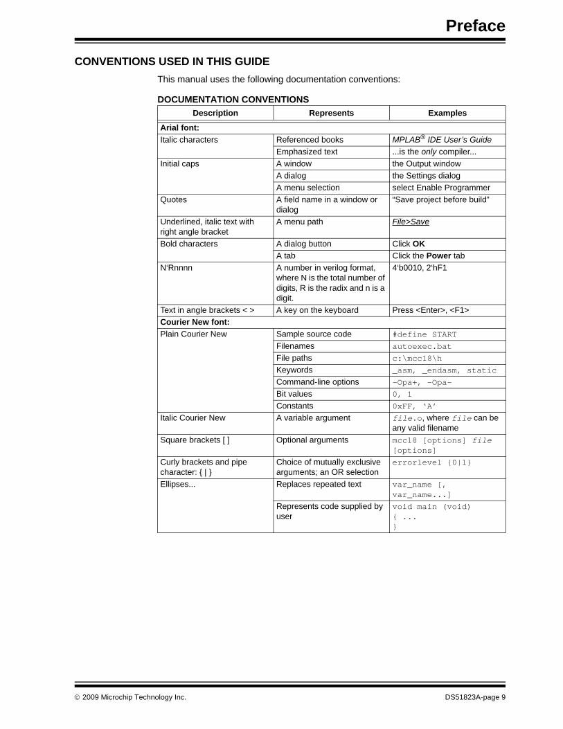
CONVENTIONS USED IN THIS GUIDEThis manual uses the following documentation conventions:
DOCUMENTATION CONVENTIONSDescription Represents Examples
Arial font:Italic characters Referenced books MPLAB® IDE User’s Guide
Emphasized text ...is the only compiler...Initial caps A window the Output window
A dialog the Settings dialogA menu selection select Enable Programmer
Quotes A field name in a window or dialog
“Save project before build”
Underlined, italic text with right angle bracket
A menu path File>Save
Bold characters A dialog button Click OKA tab Click the Power tab
N‘Rnnnn A number in verilog format, where N is the total number of digits, R is the radix and n is a digit.
4‘b0010, 2‘hF1
Text in angle brackets < > A key on the keyboard Press <Enter>, <F1>Courier New font:Plain Courier New Sample source code #define START
Filenames autoexec.batFile paths c:\mcc18\h
Keywords _asm, _endasm, static
Command-line options -Opa+, -Opa-Bit values 0, 1
Constants 0xFF, ‘A’
Italic Courier New A variable argument file.o, where file can be any valid filename
Square brackets [ ] Optional arguments mcc18 [options] file [options]
Curly brackets and pipe character: { | }
Choice of mutually exclusive arguments; an OR selection
errorlevel {0|1}
Ellipses... Replaces repeated text var_name [, var_name...]
Represents code supplied by user
void main (void){ ...}
© 2009 Microchip Technology Inc. DS51823A-page 9

MCP3909 / dsPIC33F 3-Phase Energy Meter Reference Design
RECOMMENDED READINGThis user's guide describes how to use MCP3909 / dsPIC33F 3-Phase Energy Meter Reference Design. Other useful documents are listed below. The following Microchip documents are available and recommended as supplemental reference resources.MCP3909 Data Sheet, “Energy Metering IC with SPI Interface and Active Power Pulse Output“ (DS22025)This data sheet provides detailed information regarding the MCP3909 device.AN994 Application Note “IEC61036 Meter Design using the MCP3905/6 Energy Metering Devices” (DS00994)This application note documents the design decisions associated with using the MCP390X devices for energy meter design and IEC compliance.
THE MICROCHIP WEB SITEMicrochip provides online support via our web site at www.microchip.com. This web site is used as a means to make files and information easily available to customers. Accessible by using your favorite Internet browser, the web site contains the following information:• Product Support – Data sheets and errata, application notes and sample
programs, design resources, user’s guides and hardware support documents, latest software releases and archived software
• General Technical Support – Frequently Asked Questions (FAQs), technical support requests, online discussion groups, Microchip consultant program member listing
• Business of Microchip – Product selector and ordering guides, latest Microchip press releases, listing of seminars and events, listings of Microchip sales offices, distributors and factory representatives
CUSTOMER SUPPORTUsers of Microchip products can receive assistance through several channels:• Distributor or Representative• Local Sales Office• Field Application Engineer (FAE)• Technical SupportCustomers should contact their distributor, representative or field application engineer (FAE) for support. Local sales offices are also available to help customers. A listing of sales offices and locations is included in the back of this document.Technical support is available through the web site at: http://support.microchip.com
DOCUMENT REVISION HISTORY
Revision A (November 2009)• Initial Release of this Document.
DS51823A-page 10 © 2009 Microchip Technology Inc.

MCP3909 / DSPIC33F 3-PHASEENERGY METER REFERENCE DESIGN
Chapter 1. Meter Overview
1.1 INTRODUCTIONThe MCP3909 / dsPIC33F 3-Phase Energy Meter Reference Design is a fully functional energy meter with many advanced features such as harmonic analysis, per phase distortion information, voltage sag detection, four quadrant energy measure-ment, and active and reactive power calculation. It uses Microchip’s powerful 16-bit dsPIC33F Microcontroller Unit (MCU).The MCP3909 / dsPIC33F 3-Phase Energy Meter Reference Design is unique in the fact that all calculations take advantage of the dsPIC33F DSP engine, and all output quantities are calculated in the frequency domain through the use of direct fourier transforms (DFT). This approach yields a large volume of outputs for a variety of meter designs, from simple active power only energy meters, to advanced energy meters requiring harmonic analysis.Another significant advantage of this design, is that the dsPIC firmware implements a quasi-synchronous sampling algorithm, eliminating the need for external zero-crossing detection and PLL (Phase Locked Loop) circuit for the synchronization of ADC samples to line frequency. The line frequency is measured in software and corrected for mea-surement errors caused by frequency fluctuations in the power grid. This additional processing on the dsPIC reduces the overall meter cost by eliminating the requirement for a PLL circuit.
1.2 METER DESIGN PARAMETERS• Accuracy Class: 0.2S• Rated Current Ib: 3 X 5(20)A• 3-phase 4-wire System• Line Frequency Range: 47-53 Hz or 57-63 Hz
(firmware option, see Appendix D. “50/60 Hz Meter Operation”)• ADC Sampling Rate: 12.8 ksps to 3.2 ksps• Voltage Input:
- 3 x 220/380V- 3 x 57.7/100V (3-Phase, 4-Wire)
• Starting Current: 0.001 IB• Active Power Measurement Range: 0-13200W, Precision Class: 0.2.• Reactive Power Measurement Range: 0-13200VAR, Precision Class: 0.2.• Power Factor (PF) Precision Class: 0.2.• Frequency Measurement: Precision Class: 0.2, Max. Error 0.1 Hz• Harmonic Component Measurement of Voltage Input: 2ND-31ST Harmonic• Harmonic Component Measurement of Current Input: 2ND-31ST Harmonic• Creeping: Anti-creeping Design (<0.0008 IB)• Two Pulse Outputs: Total Phase Active Power, Total Phase Reactive Power• Pulse Constant: 3200 Imp/kWh
© 2009 Microchip Technology Inc. DS51723A-page 11

MCP3909 / dsPIC33F 3-Phase Energy Meter Reference Design
1.3 POWER CALCULATIONSA summary of all the calculations performed by this energy meter are summarized below. Chapter 3. “Firmware” provides an explanation on the firmware implementation, Appendix C. “Power Calculation Theory” is included to show the theory behind this firmware.• Power Grid Frequency• RMS Voltage Of Each Phase• RMS Current Of Each Phase• RMS Neutral Current• Active Power Of Each Phase• Reactive Power Of Each Phase• Apparent Power Of Each Phase• Power Factor Of Each Phase• Fundamental Active Power Of Each Phase• Fundamental Reactive Power Of Each Phase• Harmonic Active Power Of Each Phase• Harmonic Reactive Power Of Each Phase• Total Active Power:
- The Algebraic Sum Of Active Power Of Three Phases• Total Reactive Power:
- The Algebraic Sum Of Reactive Power Of Three Phases• Total Apparent Power:
- The Algebraic Sum Of Apparent Power Of Three Phases• Total Power Factor• Phase Missing / Line voltage sag detection and alarm • Total Active Energy:
- The Algebraic Sum Of Positive/negative Active Energy• Positive/negative Active Energy• Positive/negative Reactive Energy• Four-quadrant Reactive Energy• Voltage/current Harmonic Content Of Each Phase
DS51723A-page 12 © 2009 Microchip Technology Inc.
Meter Overview
.
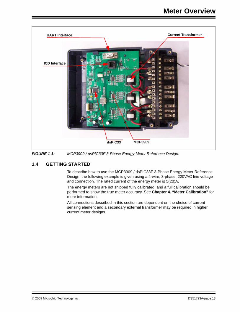
FIGURE 1-1: MCP3909 / dsPIC33F 3-Phase Energy Meter Reference Design.
1.4 GETTING STARTEDTo describe how to use the MCP3909 / dsPIC33F 3-Phase Energy Meter Reference Design, the following example is given using a 4-wire, 3-phase, 220VAC line voltage and connection. The rated current of the energy meter is 5(20)A. The energy meters are not shipped fully calibrated, and a full calibration should be performed to show the true meter accuracy. See Chapter 4. “Meter Calibration” for more information.All connections described in this section are dependent on the choice of current sensing element and a secondary external transformer may be required in higher current meter designs.
dsPIC33 MCP3909
ICD Interface
UART Interface Current Transformer
© 2009 Microchip Technology Inc. DS51723A-page 13

MCP3909 / dsPIC33F 3-Phase Energy Meter Reference Design
Step 1: Connect the meter to 220V line and loadThe diagram below shows where the voltage and current connections should be made. It is not required to connect all 3 phases for the meter to be operational.220VAC should be placed between either VA, VB, VC and NIN, NOUT.The AC load for a given phase should then be connected to the IIN and IOUT of a given phase.
FIGURE 1-2: Meter Case Bottom.
Step 2: Turn On Line/Load Power to the Meter Turn on the power to the energy meter. D1 should be lit showing the meter has power. At this point, if a load is connected and the meter is measuring power, the power LED, D1, should be blinking.
IAIN IAOUTVA IBIN IBOUTVB ICIN ICOUTVC
DS51723A-page 14 © 2009 Microchip Technology Inc.
Meter Overview
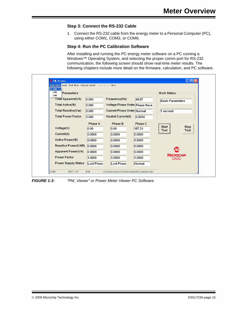
Step 3: Connect the RS-232 Cable1. Connect the RS-232 cable from the energy meter to a Personal Computer (PC),
using either COM1, COM2, or COM6.
Step 4: Run the PC Calibration SoftwareAfter installing and running the PC energy meter software on a PC running a Windows™ Operating System, and selecting the proper comm port for RS-232 communication, the following screen should show real-time meter results. The following chapters include more detail on the firmware, calculation, and PC software.
.
FIGURE 1-3: “PM_Viewer” or Power Meter Viewer PC Software.
© 2009 Microchip Technology Inc. DS51723A-page 15

MCP3909 / dsPIC33F 3-Phase Energy Meter Reference Design
NOTES:
DS51723A-page 16 © 2009 Microchip Technology Inc.
MCP3909 / DSPIC33F 3-PHASEENERGY METER REFERENCE DESIGN
Chapter 2. Hardware Description
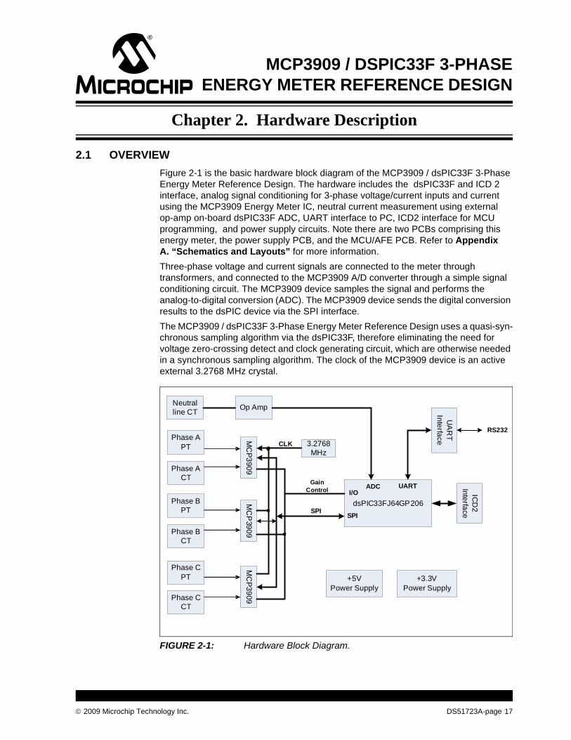
2.1 OVERVIEWFigure 2-1 is the basic hardware block diagram of the MCP3909 / dsPIC33F 3-Phase Energy Meter Reference Design. The hardware includes the dsPIC33F and ICD 2 interface, analog signal conditioning for 3-phase voltage/current inputs and current using the MCP3909 Energy Meter IC, neutral current measurement using external op-amp on-board dsPIC33F ADC, UART interface to PC, ICD2 interface for MCU programming, and power supply circuits. Note there are two PCBs comprising this energy meter, the power supply PCB, and the MCU/AFE PCB. Refer to Appendix A. “Schematics and Layouts” for more information.Three-phase voltage and current signals are connected to the meter through transformers, and connected to the MCP3909 A/D converter through a simple signal conditioning circuit. The MCP3909 device samples the signal and performs the analog-to-digital conversion (ADC). The MCP3909 device sends the digital conversion results to the dsPIC device via the SPI interface.The MCP3909 / dsPIC33F 3-Phase Energy Meter Reference Design uses a quasi-syn-chronous sampling algorithm via the dsPIC33F, therefore eliminating the need for voltage zero-crossing detect and clock generating circuit, which are otherwise needed in a synchronous sampling algorithm. The clock of the MCP3909 device is an active external 3.2768 MHz crystal..
FIGURE 2-1: Hardware Block Diagram.
SPI
RS232Phase A
PT
Phase A CT
Phase B PT
Phase B CT
Phase C PT
Phase C CT
MC
P3909M
CP
3909M
CP3909
dsPIC33FJ64GP206
CLK 3.2768MHz
UA
RT
Interface
+5VPower Supply
ICD
2 Interface
ADCI/O
SPI
UART
Neutral line CT
Gain Control
Op Amp
+3.3VPower Supply
© 2009 Microchip Technology Inc. DS51723A-page 17

MCP3909 / dsPIC33F 3-Phase Energy Meter Reference Design
2.2 ANALOG FRONT END CIRCUITRYFor safety, current transformers are used between the voltage and current input signals and the measurement module to isolate it from the 3-phase power supply.The transformer used for the voltage path is a 1:1 transformer, SPT204B from Beijing Singure Measurement & Control Technology Co., with non-linearity less than 0.1%, and rated input/output current of 2 mA/2 mA.The transformer used on the current side is a SPT254FK, from Yhehua Shanghai, with rated input /output current of 20A/2 mA, non-linearity less than 0.1%, and linear range of 0-20 A. See Appendix B. “Bill Of Materials (BOM)” for more information on the input circuitry.Using phase A as an example for the voltage signal path, a 150 kΩ (R1) resistor is used before the CT to transform the signal to an appropriate current. After the CT, burden resistors R125 and R126 are needed to transform the current signal to a differential volt-age signal for the MCP3909 device to sample. Signals are coupled into the MCP3909 device's signal input port via R110 and R111. C111 and C112 are used to filter high-fre-quency signals. Using phase A as an example for the current signal path, transformation of the current signal is similar to that of the voltage signal. The burden resistors R125/R126 and R116/R117 are chosen to be 20Ω for the current channel and 100Ω for the voltage channel after considering the following 3 factors:• The MCP3909 device's differential voltage input range: 1V for voltage channel
and 0.705V for current channel• Maximum current/voltage for the meter: rated current of 5A, maximum current of
20A, and maximum voltage of 300V)• Transformer ratio for the current and voltage transformer.A non-isolated voltage input circuit is included. In practice, a voltage divider network of resistors is often used for sampling AC voltage input. This measuring method is therefore included in the hardware design. In Figure 2-2, voltage divider resistors R3, R4, and sampling resistor R1 construct a network for sampling AC voltage.
FIGURE 2-2: Input Signal Conditioning Circuit (Phase A).
1 nF
1.0 kΩ
1 nF
1.0 kΩ
20 Ω
20 Ω
MCP3909
CH0+
CH0-
CH1+
CH1+
CTA-1SCT220B
T103
R125
R126
R110
R111
C111
C112
1 nF
1.0 kΩ
1 nF
1.0 kΩ
100 Ω
100 Ω
PA
N
SPT204B
T1
R116
R117
R108
R109
C109
C110
150 kΩ
R1
CURRENT
499 kΩ
R4
499 kΩ
R3
1 kΩR1
VOLTAGE
PA
N
33 nFC3
Jumper
VOLTAGE (Non-Isolated Option)
CTA-2
DS51723A-page 18 © 2009 Microchip Technology Inc.

Hardware Description
2.2.1 Burden Resistor Temperature CoefficientThe high precision class 0.2S requirement for the energy meter makes it crucial to select proper burden resistors for the output of the current transformers.Metal film resistors with low inherent noise and temperature coefficient are ideal. Given that the secondary current of the CT is I, then the input voltage of the MCP3909 device is U = IR, where R is the resistance of R125 and R126 (Using Phase A as an example). If the temperature varies by ΔT, and the temperature coefficient of sampling resistor R is β ppm/°C, then the output voltage is:
EQUATION 2-1:
The voltage variation is:
EQUATION 2-2:
This relationship shows that the output voltage variation caused by temperature variation is in proportion to the temperature coefficient of the burden resistor.In addition, a smaller temperature coefficient benefits meter start stabilization after startup. It takes a longer time for resistors with larger temperature coefficient to stabilize. Therefore, accurate measurements would require a longer wait after power-up. This affects the efficiency, or speed of meter calibration.
U' I R ΔT β× R×+( )=
ΔU U' U– I ΔT β× R×× U ΔT× β×= = =
© 2009 Microchip Technology Inc. DS51723A-page 19
MCP3909 / dsPIC33F 3-Phase Energy Meter Reference Design
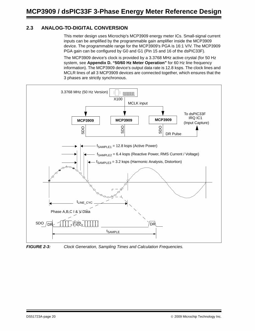
2.3 ANALOG-TO-DIGITAL CONVERSIONThis meter design uses Microchip's MCP3909 energy meter ICs. Small-signal current inputs can be amplified by the programmable gain amplifier inside the MCP3909 device. The programmable range for the MCP3909's PGA is 16:1 V/V. The MCP3909 PGA gain can be configured by G0 and G1 (Pin 15 and 16 of the dsPIC33F).The MCP3909 device's clock is provided by a 3.3768 MHz active crystal (for 50 Hz system, see Appendix D. “50/60 Hz Meter Operation” for 60 Hz line frequency information). The MCP3909 device's output data rate is 12.8 ksps. The clock lines and MCLR lines of all 3 MCP3909 devices are connected together, which ensures that the 3 phases are strictly synchronous.
FIGURE 2-3: Clock Generation, Sampling Times and Calculation Frequencies.
MCP3909 MCP3909 MCP3909
X100
3.3768 MHz (50 Hz Version)
fSAMPLE1 = 12.8 ksps (Active Power)
tLINE_CYC
SDO DR
Phase A,B,C I & V Data
16 bits DR
tSAMPLE
MCLK input
DR Pulse
To dsPIC33F
SDO
SD
O
SD
O
IRQ IC1
x 6 ADCs
(Input Capture)
fSAMPLE2 = 6.4 ksps (Reactive Power, RMS Current / Voltage)
fSAMPLE3 = 3.2 ksps (Harmonic Analysis, Distortion)
DS51723A-page 20 © 2009 Microchip Technology Inc.

Hardware Description
2.3.1 Samples And ProcessingInput capture IC1 on the dsPIC33F is used to detect if A/D conversion is complete. However, not all MCP3909 device samples are stored in the MCU, depending on the parameter being calculated. The ADC conversion rate of the MCP3909 device is determined by the frequency of the master clock (3.378 MHz for the case of a 50 Hz line), and the output data rate is MCLK/256 or 12.8 ksps. After each conversion is complete, a Data Ready signal is generated by the SDO of the MCP3909 device. The signal is fed into IC1, allowing the Interrupt Service Routine (ISR) of IC1 to read the data. When the MCP3909 device outputs data, it first sends an ADC result of the voltage channel, then an ADC result of the current channel, with MSB first.As noted, not all MCP3909 device samples are used for calculating all the parameters. In practice, 6.4 ksps sampling rate is required, which means only 1 output data is used for every 2 data sampled. For 50 Hz input signal, 6.4 ksps sampling rate will take 128 samples for each cycle. For example, the active power metering is computed based on this condition. But for other parameters for which precision is not critical, such as reactive energy, voltage, current and frequency, the sampling rate may be reduced to save data storage space and processing time. In this design, the 3.2 ksps sampling rate is used, which means only 1 result is stored for every 4 ADC conversions.After each conversion, a positive pulse with the width of 4 clock cycles is output by the SDO pin of the MCP3909 device. IC1 is used to detect the falling edge of the pulse and generate an interrupt for every 2 falling edges, i.e., 1 data is read for every 2 conver-sions, thus realizing 6.4 ksps sampling rate.
© 2009 Microchip Technology Inc. DS51723A-page 21
MCP3909 / dsPIC33F 3-Phase Energy Meter Reference Design
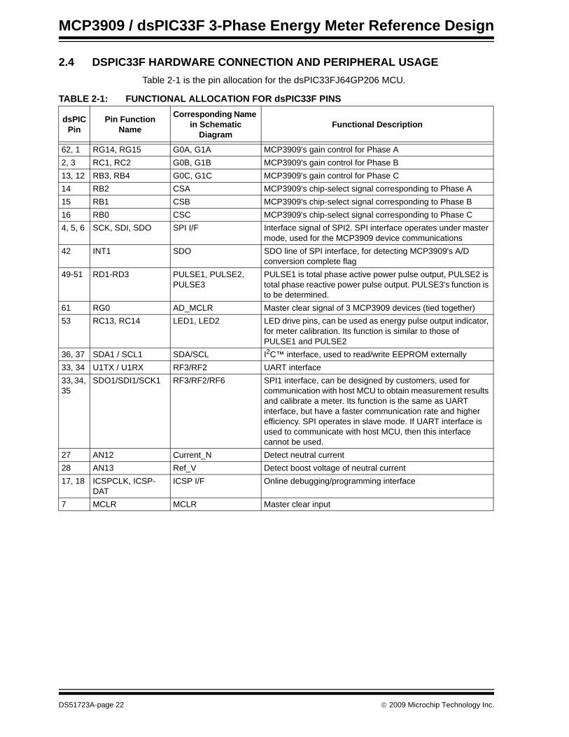
2.4 DSPIC33F HARDWARE CONNECTION AND PERIPHERAL USAGETable 2-1 is the pin allocation for the dsPIC33FJ64GP206 MCU.
TABLE 2-1: FUNCTIONAL ALLOCATION FOR dsPIC33F PINS
dsPICPin
Pin Function Name
Corresponding Name in Schematic
Diagram Functional Description
62, 1 RG14, RG15 G0A, G1A MCP3909's gain control for Phase A 2, 3 RC1, RC2 G0B, G1B MCP3909's gain control for Phase B13, 12 RB3, RB4 G0C, G1C MCP3909's gain control for Phase C 14 RB2 CSA MCP3909's chip-select signal corresponding to Phase A15 RB1 CSB MCP3909's chip-select signal corresponding to Phase B16 RB0 CSC MCP3909's chip-select signal corresponding to Phase C4, 5, 6 SCK, SDI, SDO SPI I/F Interface signal of SPI2. SPI interface operates under master
mode, used for the MCP3909 device communications42 INT1 SDO SDO line of SPI interface, for detecting MCP3909's A/D
conversion complete flag49-51 RD1-RD3 PULSE1, PULSE2,
PULSE3PULSE1 is total phase active power pulse output, PULSE2 is total phase reactive power pulse output. PULSE3's function is to be determined.
61 RG0 AD_MCLR Master clear signal of 3 MCP3909 devices (tied together)53 RC13, RC14 LED1, LED2 LED drive pins, can be used as energy pulse output indicator,
for meter calibration. Its function is similar to those of PULSE1 and PULSE2
36, 37 SDA1 / SCL1 SDA/SCL I2C™ interface, used to read/write EEPROM externally33, 34 U1TX / U1RX RF3/RF2 UART interface33, 34, 35
SDO1/SDI1/SCK1 RF3/RF2/RF6 SPI1 interface, can be designed by customers, used for communication with host MCU to obtain measurement results and calibrate a meter. Its function is the same as UART interface, but have a faster communication rate and higher efficiency. SPI operates in slave mode. If UART interface is used to communicate with host MCU, then this interface cannot be used.
27 AN12 Current_N Detect neutral current28 AN13 Ref_V Detect boost voltage of neutral current17, 18 ICSPCLK, ICSP-
DATICSP I/F Online debugging/programming interface
7 MCLR MCLR Master clear input
DS51723A-page 22 © 2009 Microchip Technology Inc.
Hardware Description
2.4.1 UART and SPI1 InterfaceThe UART and SPI1 interfaces are multiplexed. Through the UART or SPI1 interface, the host MCU can communicate with the metering front-end to perform calibration or obtain metering results. The SPI interface may also be used if high-speed data transfer is desired. In this case, the SPI interface of the dsPIC device works in the slave mode. The UART and SPI1 share a common pin, so only one of the two interfaces can be used at a time. Since the reference design uses a PC to simulate the host MCU, the UART interface is chosen as the communication interface. SPI and RS232 interfaces are not isolated from the PC. A general-purpose transceiver device, MAX232, is used for the UART interface.
2.4.2 Energy Pulse Output InterfaceThree sets of outputs for energy measurement pulses are available in this design, corresponding to the I/O pins of RD1-RD3. Two of them, output total active energy and total reactive energy, respectively, and the other is not yet specified. Outputs are isolated by a photo-electronic coupling device, U3. The photo-electronic coupler is active when corresponding I/O pin is high.In addition, the design also provides two sets of LED outputs for energy meter calibra-tion. The output pins for these LEDs are RC13 and RC14. The LED is on when the output is low. Figure 2-4 is the circuit of energy pulse output interface.
FIGURE 2-4: Energy Output Pulse Configuration.
RD3
RD2
RD1
RC13
RC14
1 kΩ
R301
1 kΩ
R301
1 kΩ
R301
470ΩR314
3.3V
470ΩR310
3.3V
D303
D302
Total Active
Total Reactive
(not used)
Total Active
Total Reactive
© 2009 Microchip Technology Inc. DS51723A-page 23
MCP3909 / dsPIC33F 3-Phase Energy Meter Reference Design
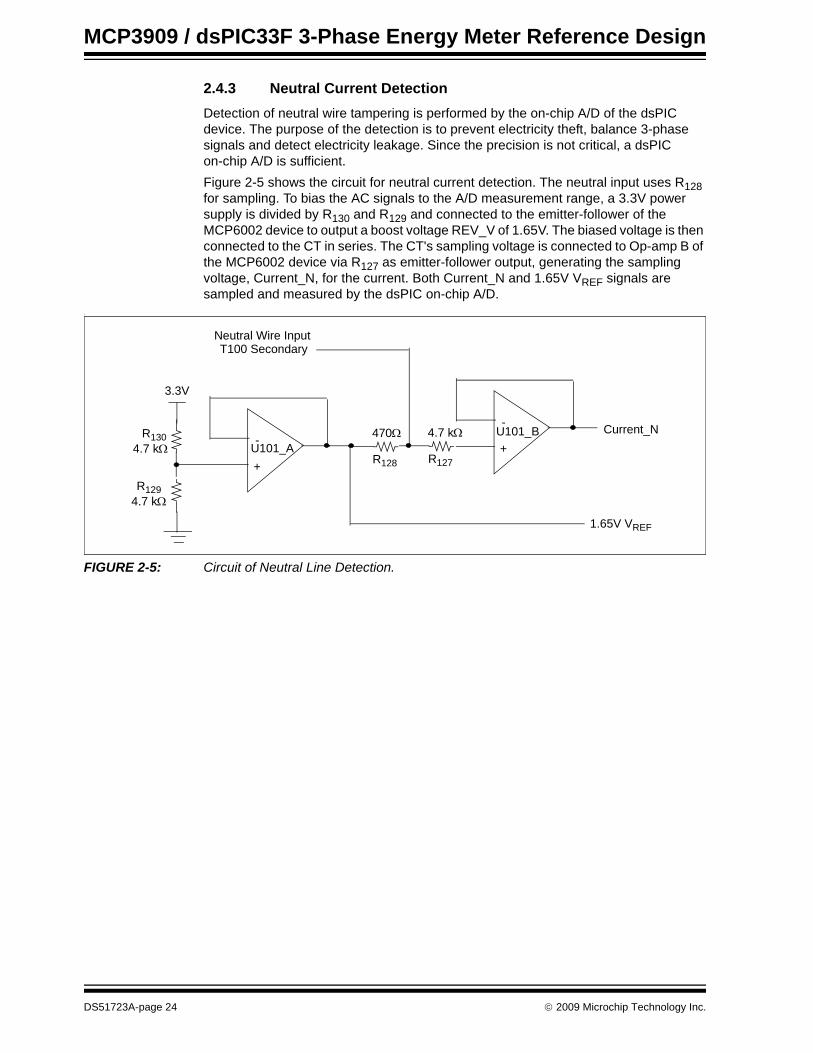
2.4.3 Neutral Current DetectionDetection of neutral wire tampering is performed by the on-chip A/D of the dsPIC device. The purpose of the detection is to prevent electricity theft, balance 3-phase signals and detect electricity leakage. Since the precision is not critical, a dsPIC on-chip A/D is sufficient.Figure 2-5 shows the circuit for neutral current detection. The neutral input uses R128 for sampling. To bias the AC signals to the A/D measurement range, a 3.3V power supply is divided by R130 and R129 and connected to the emitter-follower of the MCP6002 device to output a boost voltage REV_V of 1.65V. The biased voltage is then connected to the CT in series. The CT's sampling voltage is connected to Op-amp B of the MCP6002 device via R127 as emitter-follower output, generating the sampling voltage, Current_N, for the current. Both Current_N and 1.65V VREF signals are sampled and measured by the dsPIC on-chip A/D.
.
FIGURE 2-5: Circuit of Neutral Line Detection.
R130
R129
-
+Current_N
-
+
1.65V VREF
4.7 kΩ
4.7 kΩ
4.7 kΩ
R127
3.3V
U101_BU101_A
470Ω
R128
T100 SecondaryNeutral Wire Input
DS51723A-page 24 © 2009 Microchip Technology Inc.
Hardware Description
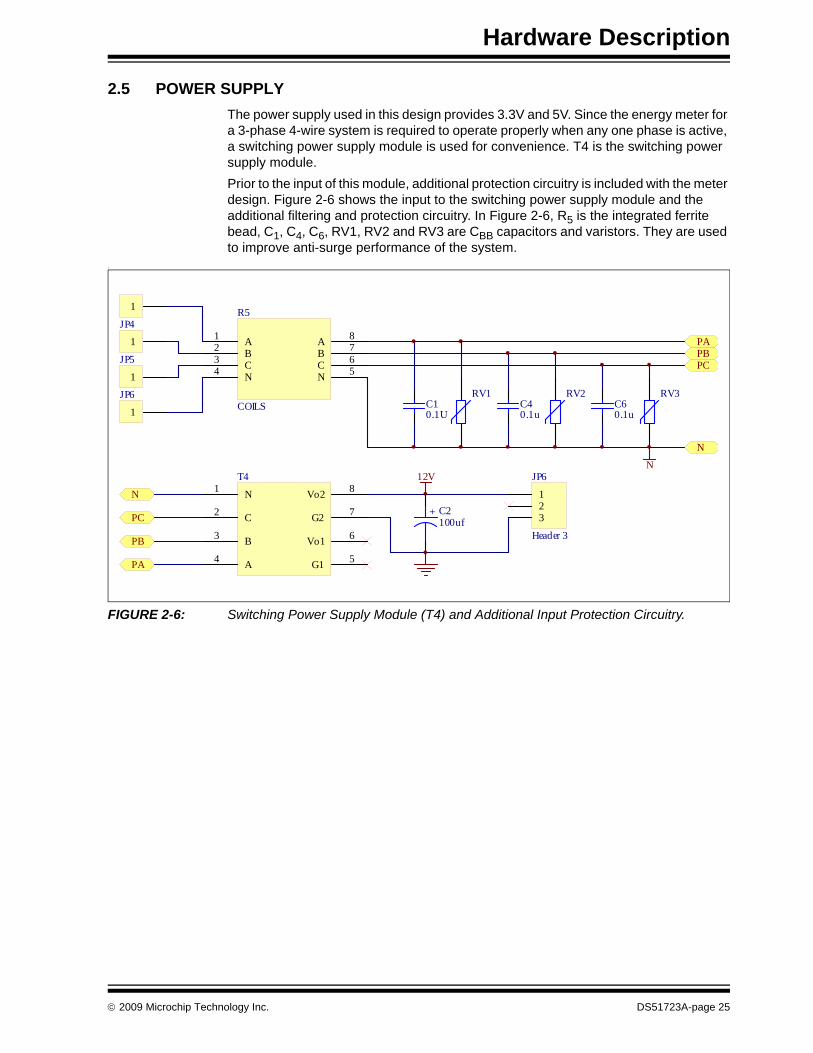
2.5 POWER SUPPLYThe power supply used in this design provides 3.3V and 5V. Since the energy meter for a 3-phase 4-wire system is required to operate properly when any one phase is active, a switching power supply module is used for convenience. T4 is the switching power supply module.Prior to the input of this module, additional protection circuitry is included with the meter design. Figure 2-6 shows the input to the switching power supply module and the additional filtering and protection circuitry. In Figure 2-6, R5 is the integrated ferrite bead, C1, C4, C6, RV1, RV2 and RV3 are CBB capacitors and varistors. They are used to improve anti-surge performance of the system.
.
FIGURE 2-6: Switching Power Supply Module (T4) and Additional Input Protection Circuitry.
1
JP5
1
JP4
1
1
JP6
N1
C2
B3
A4 G1 5
Vo1 6
G2 7
Vo2 8T4
RV3RV1 RV2
A1
B2
C3
N4 N 5C 6B 7A 8
R5
COILS
12V
C40.1u
C10.1U
C60.1u
PAPBPC
N
PA
PB
PC
N
N
123
JP6
Header 3
+ C2100uf
© 2009 Microchip Technology Inc. DS51723A-page 25
MCP3909 / dsPIC33F 3-Phase Energy Meter Reference Design
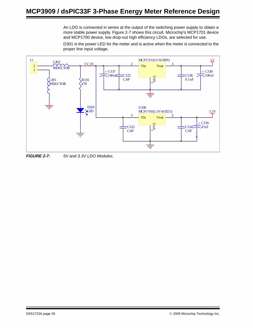
An LDO is connected in series at the output of the switching power supply to obtain a more stable power supply. Figure 2-7 shows this circuit. Microchip's MCP1701 device and MCP1700 device, low drop-out high efficiency LDOs, are selected for use.D301 is the power LED for the meter and is active when the meter is connected to the proper line input voltage.
FIGURE 2-7: 5V and 3.3V LDO Modules.
C322CAP
C3360.1uF
+ C337100uf
5V
C323CAP
C324CAP
+ C338100uf
+ C33947uF
D301LED
R316470
Vin3 Vout 2
Gnd1
U306MCP1700(3.3V-SOT23)
12
J15V_IN
3.3V
L302
INDUCTOR
L301INDUCTOR
Vin2 Vout 3
VSS1
MCP1701(5V-SOT89)
DS51723A-page 26 © 2009 Microchip Technology Inc.
MCP3909 / DSPIC33F 3-PHASEENERGY METER REFERENCE DESIGN
Chapter 3. Firmware
3.1 OVERVIEWThis section discusses the dsPIC firmware structure, peripheral resources, important program flows, and explanations of project files included in the firmware zip files included with the system. See Appendix D. “50/60 Hz Meter Operation” for converting to 60 Hz code.• Calculate all electrical parameters in frequency domain• MCP3909 device communication• Detect voltage/current phase order, and determine missing phases• Generation imp/kWh power pulse• UART communication
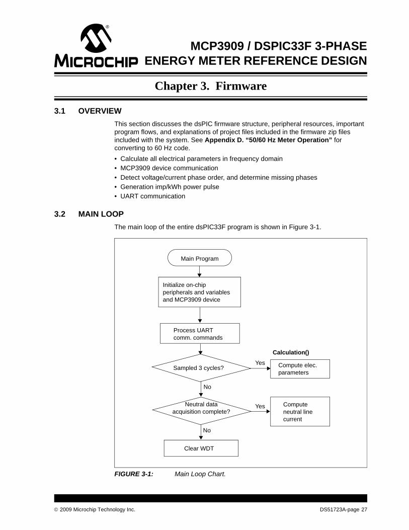
3.2 MAIN LOOPThe main loop of the entire dsPIC33F program is shown in Figure 3-1.
FIGURE 3-1: Main Loop Chart.
Main Program
Initialize on-chip peripherals and variables
Process UART comm. commands
Sampled 3 cycles? Compute elec.parameters
Neutral dataacquisition complete?
Clear WDT
Computeneutral line current
Yes
No
Yes
No
and MCP3909 device
Calculation()
© 2009 Microchip Technology Inc. DS51723A-page 27

MCP3909 / dsPIC33F 3-Phase Energy Meter Reference Design
After system power-up, the MCU enters the initialization process, which includes proper configuration of the I/O ports and on-chip peripherals (such as timer, UART, SPI and IC). At the same time, the system control parameters can be loaded from the external EEPROM and variables are all initialized.Since most tasks of this system are accomplished through interrupts, only three tasks are carried out in the system main loop, which are interpreting/processing UART communication protocol, calculating parameters, and detecting neutral current. The UART communication is performed in function UART_process(), the executing frequency of which depends on the polling frequency of the upper computer.Parameters are calculated by the function Calculation(), which is executed once every 3 cycles of the power grid. Neutral current is detected by function ComputeNeutral-Current(), and computing is performed once every 16 cycles of the power grid.
DS51723A-page 28 © 2009 Microchip Technology Inc.
Firmware
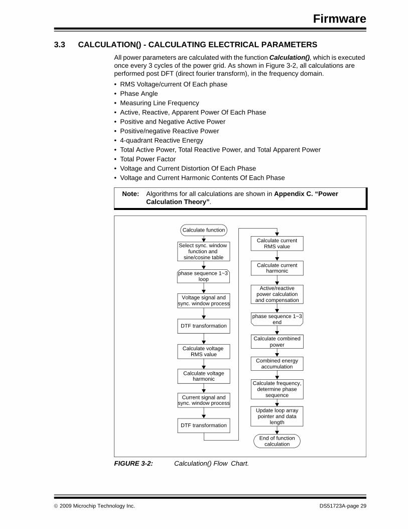
3.3 CALCULATION() - CALCULATING ELECTRICAL PARAMETERS All power parameters are calculated with the function Calculation(), which is executed once every 3 cycles of the power grid. As shown in Figure 3-2, all calculations are performed post DFT (direct fourier transform), in the frequency domain. • RMS Voltage/current Of Each phase• Phase Angle• Measuring Line Frequency• Active, Reactive, Apparent Power Of Each Phase• Positive and Negative Active Power• Positive/negative Reactive Power• 4-quadrant Reactive Energy• Total Active Power, Total Reactive Power, and Total Apparent Power• Total Power Factor• Voltage and Current Distortion Of Each Phase• Voltage and Current Harmonic Contents Of Each Phase
FIGURE 3-2: Calculation() Flow Chart.
Note: Algorithms for all calculations are shown in Appendix C. “Power Calculation Theory”.
Calculate function
Select sync. window function and
sine/cosine table
phase sequence 1~3 loop
Voltage signal andsync. window process
DTF transformation
Calculate voltage
Calculate voltageharmonic
Current signal andsync. window process
DTF transformation
RMS value
Calculate current
Calculate currentharmonic
RMS value
Active/reactivepower calculationand compensation
phase sequence 1~3end
Calculate combinedpower
Combined energyaccumulation
Calculate frequency,determine phase
sequence
Update loop arraypointer and data
length
End of functioncalculation
© 2009 Microchip Technology Inc. DS51723A-page 29
MCP3909 / dsPIC33F 3-Phase Energy Meter Reference Design
Each block can be categorized into one of three types of calculations: 1. Calculation for an individual phase2. Calculation for all 3 phases3. Calculation of power accumulation (Energy)
3.3.1 Process Quasi-Synchronization WindowThe first blocks of the calculation flow are to determine how many samples to use for the quasi-synchronization sampling algorithm. See Appendix C. “Power Calculation Theory” for more information on this approach. The firmware selects the proper quasi-synchronization window function (array of data) and corresponding sine/cosine table according to the number of sampling points in present current cycle.The number of sampling points is obtained from the last calculation of frequency function. As the line frequency fluctuates in slow motion and typically varies by a small amount over three (3) line cycles, the period of line frequency measurements of the previous cycle can be used to determine data length of sampling.The quasi-synchronization window function is an array established in advance, and its length is the same as that of the sampling data, which is obtained by the weight coefficient multiplied by 32768. In this design, the method of quadrature by complexification echelon is used, corresponding weight coefficient is calculated with three (3) iterations. Three iterations implies that the length of the input original data is equal to the number of sampling points in three cycles. The number of sampling points in each cycle is usually different from the input signal cycle, but it will be close to an integral multiple of the input signal cycle. For example, at a sampling rate of 3.2 ksps, 50 Hz input signal corresponds to 64 sampling points for each cycle, and 50.1 Hz input signal would also be close to 64 sampling points for each cycle. Again, 51 Hz input signal would be close to 63 sampling points for each cycle. Therefore, at different input frequencies, the corresponding numbers of sampling points in each cycle are different. Consequently, the corresponding quasi-sync window function and sine/cosine table need to be established according to different numbers of sampling points. The sine/cosine table is established by evenly dividing a cycle into a number of segments equal to the number of sampling points, calculating corresponding sine/cosine values and then multiplying the values by 32768. The purpose of the multiplication is to change the original operation of floating point numbers into that of fixed-point numbers. Adjustments will be performed in the final stage of calculation.The processing of the original signal being processed by the quasi-synchronization window function is actually a process of array multiplication, i.e. the original input signal is multiplied with a corresponding array of window functions. It's accomplished by the function qusi_syn_wnd(), which is written in assembly to take full advantages of DSP features.
3.3.2 DFT TransformationA Direct Fourier Transform (DFT) is performed on the collected sets of data. Process-ing of the original signal by quasi-synchronization window can effectively reduce spectrum leakage caused by non-entire-cycle sampling during DFT transformation.The data length is not a power of 2, therefore, the FFT algorithm cannot be used in DFT transformation. DFT transform is accomplished by function DFT(), which is written in assembly to take full advantages of the DSP feature of accumulated multiplication.Since an FFT algorithm cannot be used, and it takes longer to perform a DFT calculation, this is the most time-consuming process in the entire system.
DS51723A-page 30 © 2009 Microchip Technology Inc.

Firmware
3.3.3 Calculating RMS Voltage/CurrentAfter the data set of either a voltage or current signal (of each phase), has been DFT transformed, the voltage or current magnitudes of the different harmonics can then be calculated. The total effective voltage or current (RMS) can be obtained by further calculaton, by simply combining the results of the individual harmonics (including the fundamental or the 1ST harmonic).Computing the magnitude of the voltage or current is accomplished by function ComputeMagnitude(). The result, called amplitude, is a long integer, and is the squared magnitude of voltage or current. To speed up the computation, fixed-point operation is used. The ComputeMagnitude() routine is written in assembly language.After the magnitude is computed, there is an adjustment process which is based on a floating-point operation. The limited number of computations will not affect the operation speed, and will instead greatly improve precision.Parameter ratio1 in the firmware is a coefficient related to the number of sampling points (see Equation 2-2). Division is accomplished by a simple shift operation in firmware. If the sampling cycle is not a power of 2, it cannot be accomplished by shifting. However, division by shifting can be accomplished by multiplying a compen-sating coefficient Coeff.data.linear.V_channel[]. This is the calibration coefficient for ratio errors.Since the current signal has a wide dynamic range, for small signals, the ADC output data range is small and is limited by DSP's bit resolution (16-bit MCU). If division by shift is used in the same way that is used for large signals in computation, precision may be affected. Therefore, for computing magnitudes of small signals, ComputeS-mallMagnitude() function is used instead. This function is similar to ComputeMagni-tude(), the only difference being that the shift length is shortened in division operation, and will be compensated during data adjustment. The computation precision will not be affected as the data adjustment process uses float-point operation.
3.3.4 Calculating HarmonicsComputing harmonics is accomplished in assembly language, by the function Com-puteHarmonic(). The computation is based on Equation C-62, in Appendix C. “Power Calculation Theory”. The result is the ratio of the magnitude of K-th harmonic to fundamental magnitude, and is given in a percentage.
3.3.5 Calculating PowerComputing power is accomplished in assembly language by the function Compute-Power() based on Equation C-39 and Equation C-40 in Appendix C. “Power Calcu-lation Theory”.After the ComputePower() function is complete, an adjusting process for computed power is required. First, the computed result is adjusted according to the gain of current amplifier. Then the calibrating coefficient ratio2 is determined according to present number of sampling points.Additional compensation to the power calculation is required, for phase compensation. This compensation is based on the present load current. The difference between signal frequency and the central frequency is also taken into consideration. Consequently computed power is compensated.
Note: Since the output of ComputeHarmonic() is the squared harmonic magnitude, extraction of square root is needed in computation. The calculated harmonic content is stored as a fixed-point number, and the actual value stored is the harmonic content multiplied by 10.
© 2009 Microchip Technology Inc. DS51723A-page 31
MCP3909 / dsPIC33F 3-Phase Energy Meter Reference Design
3.3.6 Active Energy AccumulationEnergy accumulation is done by calculating the total energy, which is the algebraic sum of energy of each phase. Active energy is obtained by accumulating the multiplication of voltage and current of each sample, which ensures the high accuracy of measure-ment.
3.3.7 Reactive Energy Accumulation The required measurement accuracy of reactive energy low, so in this design, it is obtained by accumulating the product of the present measured reactive power and the time interval between two measurements.
3.3.8 Output Pulse GenerationRefer to Section 2.4.2 “Energy Pulse Output Interface” for pulse output. To ensure the uniformity of output pulses, the calculation is divided in the measurement cycle into in a number of equal sections, and accumulate them. For simplification and lowering computation complexity, a counter is used to substitute the process of accumulation. The counter is only enabled when accumulated energy approaches to the threshold of the pulse output.
3.3.9 Line Frequency CalculationFrequency calculation is based on Equation C-52 and Equation C-53, in Appendix C. “Power Calculation Theory”. The dsPIC33F collects 3-line cycles worth of data. The first two cycles of data of all sampled data is analyzed, and then the frequency of two successive cycles is used.The data of two successive cycles are transformed via DFT for the fundamental, which is accomplished by assemble function DFT_Fundamental(). This is followed by the computation of the initial phase angle of the first two line cycles. Then the phase lag and frequency offset of the two line cycles of signal can be calculated.When measuring frequency, only the first two cycles of data are used. It must be assumed the input frequency is 50 Hz and the chosen appropriate sine/cosine table to carry out DFT transform for fundamentals of the 1st and 2nd cycles of data. See Appendix D. “50/60 Hz Meter Operation” for 60 Hz firmware.Frequency offset is calculated by determining the initial phase angle for each line cycle. The greater the frequency offset, the greater the measurement error. Since one of the 3 phases may be missing, if the voltage magnitude for phase A is less than the threshold, it is necessary to switch to phase B. Consequently, if sufficient volt-age magnitude of phase B is not detected, it is necessary to switch to phase C.The basic algorithm for measuring line frequency is based on the method described in Appendix A, Section C.4 “Measuring The Voltage/current Rms Value And Power Using Quasi-synchronous Sampling Algorithm”.Frequency will be measured once for every 3 times the data is sampled.
DS51723A-page 32 © 2009 Microchip Technology Inc.
Firmware
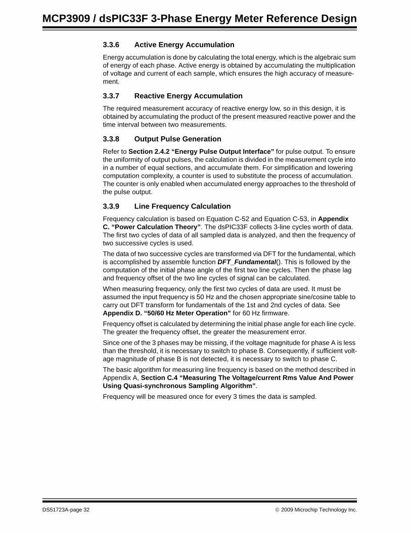
3.4 ADC SAMPLING SCHEME FOR CALCULATIONSThe ADC conversion rate of the MCP3909 device is determined by the frequency of master clock, MCLK, and the rate will be MCLK/256. After each conversion is complete, a DataReady signal (4-CLK length) is generated by the SDO of the MCP3909 device. The signal is fed into IC1 (Input Capture 1 on the dsPIC33F), allowing the Interrupt Service Routine (ISR) of IC1 to invoke data-read function of the MCP3909 device. When the MCP3909 device outputs data, it first sends the ADC result of the voltage channel, then that of the current channel, with the MSB first. The frequency of the master clock, MCLK, of the MCP3909 device is 3.2768 MHz, and ADC outputs @12.8 ksps. In practice 6.4 ksps sampling rate is used in the program, which means only 1 output data is used for every 2 data sampled. For a 50 Hz input signal, a 6.4 ksps sampling rate will take 128 samples for each cycle. The active power calculation is computed based on this condition.The other parameters for which precision is not critical, such as reactive energy, voltage, current and frequency, the sampling rate may be reduced to save data storage space and processing time. In this design, the 3.2 ksps sampling rate is used, which means only 1 result is stored for every 4 ADC conversions.In the program, sampling and calculation are carried out concurrently, and data is stored in the cyclic array in the dsPIC33F RAM. A calculation may be performed after either 1 cycle, 2 cycles or 3 cycles of data are sampled, which can be configured in the program. The user should note that frequent calculations will increase the measure-ment precision at the price of system overhead and response speed, therefore making proper tradeoffs based on practical requirement. In this design, 3 cycles of signals are sampled before an AC electrical parameter calculation is performed. Refer to Figure 3-3.
FIGURE 3-3: AC Signal Sampling alnd Computing.
3.4.1 Processing IC1 Interrupt Input capture IC1 is used to detect if the A/D conversion is complete. After each conversion, a positive pulse the width of 4 clock cycles is outputted by the SDO pin of the MCP3909 device. IC1 is used to detect the falling edge of the pulse and generate an interrupt for every 2 falling edges, i.e., 1 data is read for every 2 conversions, thus realizing 6.4 ksps sampling rate.In addition to reading the data of the MCP3909 device, the IC1 interrupt service routine (ISR) also controls the energy pulse output generation. Energy pulse processing consists of active/reactive energy pulse processing. For the pulses to be outputted more uniformly, the clock resolution used to generate the pulses must be as high as possible. The interval of the IC1 interrupt is 156.25 µs, therefore, the resolution generated by the pulse can be up to 156.25 µs.
Sampling Cycle n
Sampling Cycle n+1
Sampling Cycle n+2
Sampling Cycle n+3
Idle Idle Idle Calculate n,n+1,n+2
Sampling Cycle n+4
Idle
© 2009 Microchip Technology Inc. DS51723A-page 33

MCP3909 / dsPIC33F 3-Phase Energy Meter Reference Design
The energy pulse processing program only begins when the level is close to outputting pulse level. To simplify the process and shorten the ISR execution time, a counter is used in place of the energy accumulation function for each pulse and to determine if a pulse will be outputted. When the count is greater than the threshold of pulse output, an energy pulse will be outputted, and the appropriate amount of energy will be sub-tracted from the energy accumulating register. Output toggling will then be processed. Once the width of the output pulse exceeds 80 ms, the pulse output will be turned off.The program flow chart is shown in Figure 3-4.
FIGURE 3-4: IC1 Interrupt Service Routine.
ICI Interrupt Serviceroutine
Call MCP3909 dataread program
Processing falling edge of active energy?
Processingrising edge of active energy?
Processing falling edge of
reactive energy?
Return
Yes
Yes
Yes
Yes
No
No
No
No
Processingrising edge of active energy?
Update pulse width counter, if counter > flip threshold, output pulse and update energy accumulation register.
Update pulse width counter, if counter > flip threshold, output pulse and update energy accumulation register.
Update pulse width counter, if pulsewidth > 80 ms, toggle pulse output level. End pulse output process.
Update pulse width counter, if pulsewidth > 80 ms, toggle pulse output level. End pulse output process.
DS51723A-page 34 © 2009 Microchip Technology Inc.
Firmware
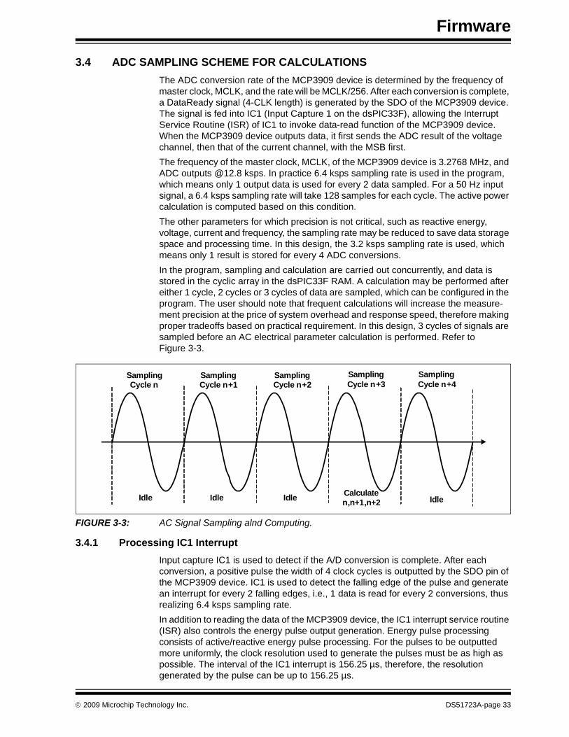
3.5 READING A/D DATA OF THE MCP3909 DEVICEAll three MCP3909 devices use the same clock source and reset signal, so all 6 A/D channels of the 3 MCP3909 devices are synchronous. Only a single Data Ready (SDO) signal of any of the MCP3909 device is required to read A/D data of the 3 phases in turn. This module is invoked by IC1 interrupt triggered by the "data ready" signal on the SDO of the MCP3909 device. IC1 is set to generate an interrupt for every two falling edges. Therefore, only one of the two sampling data of the MCP3909 device is read.The flow of reading the MCP3909 device's data is as follows:• Retrieve all values of 3-phases, both current channel and voltage channel data.
Bits 0-15 of each phase data are voltage channel data, bits 16-31 are current channel data
• Accumulate the active power of each phase. On every other interrupt, the current and voltage values are stored into RAM in the cyclic sampling array
• Update the pointer of sampling array and length of sampling data. If the length of sampling data is 3-line cycles long, set the sampling complete flag, and then the calculation function Calculate() will be called by the main flow to start computing all corresponding parameters.
FIGURE 3-5: Flow Chart of Read A/D Data.
Read MCP3909 data
Select phase A of
clear SPI flag
Even countdata read?
Read phase A dataand accumulate activeenergy of phase A
Read phase B dataand accumulate activeenergy of phase B
Read phase C dataand accumulate activeenergy of phase C
End
Read phase A data,accumulate activeenergy of phase Aand save data to array
Read phase A data,accumulate activeenergy of phase Aand save data to array
Read phase A data,accumulate activeenergy of phase Aand save data to array
Update array pointer,sample pass count flag and data length
End of sampling of this cycle?
Set data sampling complete flag
No
Yes
yNo
The MCP3909 device,
© 2009 Microchip Technology Inc. DS51723A-page 35
MCP3909 / dsPIC33F 3-Phase Energy Meter Reference Design
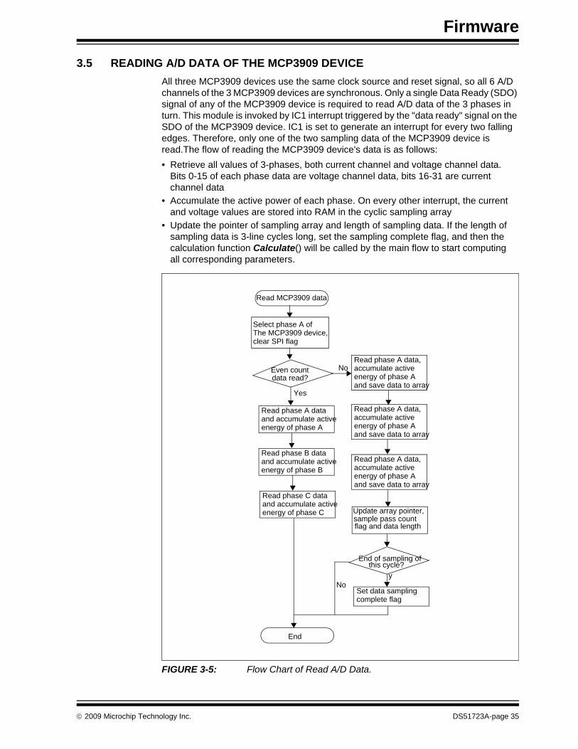
3.5.1 Initialize and Configure MCP3909 Operation ModeThe task of this module is to enable the MCP3909 device to enter the "Channel Output" mode. This design uses the "Channel Output" mode of the MCP3909 device. In this mode, the current and voltage data channels measured by the ADC is sent through the MCP3909 device's SPI port. To enable the MCP3909 device to enter the Channel Output mode, certain instructions must be sent to the device via the SPI interface within a specified time (32CLK) after resetting the MCP3909 device.• Enable all MCP3909 devices: enable ADCS1, ADCS2 and ADCS3, and configure
MCU's SPI to 8-bit mode• Reset the MCP3909 device through the RESET pin. The pin must be pulled low
for no less than 1 clock cycle of the MCP3909 device• After the RESET pin is pulled high, wait for 4 clock cycles for the MCP3909 device
pin functions to reset• Send Instruction 0x94 to the MCP3909 device through the SPI Interface• Configure the SPI interface to 16-bit mode and strobe the MCP3909 device for
Phase A
FIGURE 3-6: Initializing the MCP3909 Device Flow Chart.
Initialize MCP3909
Strobe all
Reset the
Wait for 4 CLK cycles
Send instruction 0xac
Set SPI to 16-bit mode
Strobe phase A of the MCP3909 device
End
MCP3909 devices
MCP3909 devices
DS51723A-page 36 © 2009 Microchip Technology Inc.
Firmware
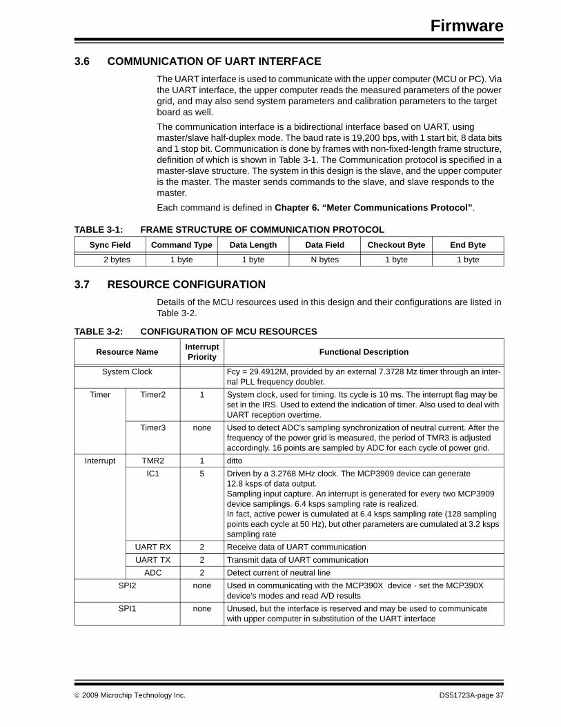
3.6 COMMUNICATION OF UART INTERFACE The UART interface is used to communicate with the upper computer (MCU or PC). Via the UART interface, the upper computer reads the measured parameters of the power grid, and may also send system parameters and calibration parameters to the target board as well.The communication interface is a bidirectional interface based on UART, using master/slave half-duplex mode. The baud rate is 19,200 bps, with 1 start bit, 8 data bits and 1 stop bit. Communication is done by frames with non-fixed-length frame structure, definition of which is shown in Table 3-1. The Communication protocol is specified in a master-slave structure. The system in this design is the slave, and the upper computer is the master. The master sends commands to the slave, and slave responds to the master.Each command is defined in Chapter 6. “Meter Communications Protocol”.
TABLE 3-1: FRAME STRUCTURE OF COMMUNICATION PROTOCOL
3.7 RESOURCE CONFIGURATIONDetails of the MCU resources used in this design and their configurations are listed in Table 3-2.
Sync Field Command Type Data Length Data Field Checkout Byte End Byte
2 bytes 1 byte 1 byte N bytes 1 byte 1 byte
TABLE 3-2: CONFIGURATION OF MCU RESOURCES
Resource Name InterruptPriority Functional Description
System Clock Fcy = 29.4912M, provided by an external 7.3728 Mz timer through an inter-nal PLL frequency doubler.
Timer Timer2 1 System clock, used for timing. Its cycle is 10 ms. The interrupt flag may be set in the IRS. Used to extend the indication of timer. Also used to deal with UART reception overtime.
Timer3 none Used to detect ADC's sampling synchronization of neutral current. After the frequency of the power grid is measured, the period of TMR3 is adjusted accordingly. 16 points are sampled by ADC for each cycle of power grid.
Interrupt TMR2 1 dittoIC1 5 Driven by a 3.2768 MHz clock. The MCP3909 device can generate
12.8 ksps of data output.Sampling input capture. An interrupt is generated for every two MCP3909 device samplings. 6.4 ksps sampling rate is realized.In fact, active power is cumulated at 6.4 ksps sampling rate (128 sampling points each cycle at 50 Hz), but other parameters are cumulated at 3.2 ksps sampling rate
UART RX 2 Receive data of UART communicationUART TX 2 Transmit data of UART communication
ADC 2 Detect current of neutral lineSPI2 none Used in communicating with the MCP390X device - set the MCP390X
device's modes and read A/D results SPI1 none Unused, but the interface is reserved and may be used to communicate
with upper computer in substitution of the UART interface
© 2009 Microchip Technology Inc. DS51723A-page 37

MCP3909 / dsPIC33F 3-Phase Energy Meter Reference Design
3.8 DESCRIPTION OF PROJECT FILES
TABLE 3-3: FILE DESCRIPTIONFile Name Description
main.hmain.c
Main program
global.hglobal.c
Mainly define important system macros, key data structures, and declare global variables.
MCP390x.h Declare macros, constants, local global variables, some of the global variables and functions used in the MCP390X device.
MCP390x.c Functions involved with the MCP390X device, including set SPI, initialize the MCP390X device and read data.
calcu.h Declare macros, constants, local global variables, some of the global variables and functions used in calcu.c.
calcu.c Main module to calculate parameters, including calculate frequencies, current/voltage RMS, power, power factors and energy, and analyze harmonics.
uart_comm.c Declare macros, constants, local global variables, some of the global variables and functions used in uart.c.
uart.c Receive, transmit, process protocol and so forth for UART communication.Calibrate.c Program for Ratio error calibration, power calibration and phase lag calibration, it stores and
initializes calibration data.Calibrate.h Declare constants, local variables and global variables used in calibration.Adc.cAdc.h
On-chip ADC operation, detecting the current of neutral wire.
I2Csubs.hI2Csubs.c
Control EEPROM of off-chip I2C interface.
interrupt.h Declare macros, constants, local global variables, some of the global variables and functions used in interrupt.c.
interrupt.c Set interrupts and ISRs.Asmcode.c Some assemble functions used in calculation.
DS51723A-page 38 © 2009 Microchip Technology Inc.
MCP3909 / DSPIC33F 3-PHASEENERGY METER REFERENCE DESIGN
Chapter 4. Meter Calibration
4.1 INTRODUCTIONMeter calibration consists of using standard electrical power equipment that supplies the power to the meter and calculates the error and correction factor at each calibration point. This equipment must be accurate in order to calibrate the energy meter. The supplied PC software is then used to send calibration commands and correction factors down to the dsPIC33F, completing meter calibration.
Why Is Calibration Necessary?An energy meter usually consists of errors due to transformers, VREF tolerance, ADC gain errors, and other passive component errors. Energy meters are factory calibrated before shipping to eliminate the impact from such elements and reduce the error. The non-linearity and inconsistency of signals in the path of sampling circuit and A/D conversion circuit cannot be ignored in high-accuracy measurement. The impact needs to be corrected to improve measurement accuracy.The calibration described in this chapter are calibrated with the help of the PC software PM_Viewer, described in detail in the next chapter. To summarize the process, the measurement error is fed into the software, and the data is then sent to the meter to via the UART. The details of this procedure are detailed in the next chapter, "PC Software".
4.2 CURRENT/VOLTAGE CALIBRATIONCurrent and voltage calibration is a ratio error calibration from the upper computer by sending commands and data for correction to the MCU. The dsPIC33F will call a firmware module after receiving the command from the host PC. The flow is as follows:1. Determine the phase to be calibrated and the magnitude of current and voltage
being applied to the meter, and read measurement (RMS) values of that channel.2. Calculate the calibration coefficient of the ratio error by the ratio of standard value
received to the measured value.3. Multiply the original coefficient by calibration coefficient and obtain the calibration
coefficient after correction.4. Store the final calibration coefficient after correction into EEPROM.
Since the dynamic range of the voltage channel is usually very small, single-point calibration is enough to meet the accuracy requirements for full range. However, the dynamic range of the current channel is larger, and the transformer has different ratio errors at different current loads.The MCP3909 device’s current channel, CH0, contains a PGA with gain options of 1, 2, 8, 16. For high-accuracy energy meters, current ratio error needs to be segmented and calibrated for different current loads. The ratio error calibration of current channel uses a two-point calibration method. One point is calibrated when the load is at the rated current (IB) and the PGA gain is 1. The second point is calibrated under small-sig-nal input condition (0.1 IB) and the PGA gain is 16.
Note: Voltage and current calibration is a two step process using 100% and 10% IB.
© 2009 Microchip Technology Inc. DS51723A-page 39
MCP3909 / dsPIC33F 3-Phase Energy Meter Reference Design
4.2.1 Current/Voltage Calibration ProcessThe process of calibration is as follows:1. Supply the meter with balanced load, PF = 1.0, VCAL = 220V, IB = 5A. 2. Load the dsPIC33F with the proper correction factors. Automatically done using
the PC software. See Chapter 5. “PC Software”. Repeat these following steps for the second point at 10% IB:1. Set the three-phase balance input conditions PF = 1.0, VCAL = 220V, ICAL = 0.1 IB or
500 mA.2. Load the dsPIC33F with the proper correction factors. Automatically done using
the PC software. See Chapter 5. “PC Software”.If accuracy is not critical, the single-point calibration method can be used. The number of calibration points can be defined in the header file of the program.
4.3 APPARENT POWER CALIBRATIONApparent Power calibration function is implemented by the upper computer by sending the commands. Before the power calibration process can be entered, power calibration mode command needs to be sent first. The error data of the calibration workbench and channel information to be calibrated are sent to the metering front-end. When the front-end receives the command, it calls this module. The flow is as follows:1. Determine the phase to be calibrated according to the parameters received.2. Calculate new power calibration coefficient according to the error value received
and the measured value, together with the original power calibration coefficient.3. Store the coefficient after correction into the EEPROM.
4.3.1 Apparent Power Calibration ProcessThe process of calibration is as follows:1. Set the input condition as: Phase A PF = 1.0, VCAL = 220V, input current is the
current when region N is being calibrated, the voltage and current inputs of phase B and C are zero.
2. Choose the energy pulse output to be the apparent power output mode Refer to Chapter 6. “Meter Communications Protocol”. At this time, the energy pulse is the accumulated multiplication of power and time.
3. Load the dsPIC33F with the proper correction factors. This is automatically done using PC software. See Chapter 5. “PC Software”.
4. Repeat steps 1 - 3 for phase lag calibrations for all current regions of phase A.
5. Repeat the above steps for Phases B and C.
Note: At this time, the phase lag has not been calibrated, so when the input PF = 1.0, the measured value of the reactive power isn't equal to zero.
DS51723A-page 40 © 2009 Microchip Technology Inc.

Meter Calibration
4.4 PHASE LAG CALIBRATION
The phase lag calibration function is implemented by the upper computer by sending the proper commands via the UART. When calibrating phase lag, error from the calibration equipment and channel information to be adjusted are sent to the dsPIC33F energy meter. When the front-end receives the command, it calls this module. The flow is as follows:1. Determine the phase to be calibrated according to parameters received.2. Calculate new phase lag calibration coef. according to the error value received
and the measured value.3. Store the coefficient after correction into the EEPROM.This meter design supports single, two, and five point calibration for phase lag error correction.The purpose of phase lag calibration is to eliminate the impact of phase lag introduced by the current transformer (CT), and voltage transformer (PT) over the power measure-ment range.The voltage transformer usually has a constant load, thereby introducing a phase lag that varies insignificantly. The dynamic range of current is larger, and under different current loads, phase lags caused by CT vary greatly. In order to meet the requirements of measurement accuracy in the entire range, it is usually necessary to segment the phase lag and calibrate.In this design, current is partitioned into 5 regions.
TABLE 4-1: CURRENT REGIONS FOR PHASE CALIBRATION
The partition limit for the current region can be modified in the header file of the program. If accuracy is not critical, single-point calibration and two-point calibration can be used to improve the efficiency of meter calibration.
Single, Two, or Five Point CalibrationSingle-, two- or five-point calibration method can be configured by modifying the header file. When using the single-point calibration, the phase lag compensation values of all regions are the same; When using two-point calibration, the compensation values of region 1 and 2 (0-0.075 IB, 0.075 IB - 0.2 IB) are the same, and the phase lag compensation values for region 3, 4 and 5 (0.2 IB - 0.75 IB, 0.75 IB - 1.5 IB, 1.5 IB - 4.0 IB) are the same.
Region Current Range
1 0 - 0.075 IB 2 0.075 IB - 0.2 IB3 0.2 IB - 0.75 IB4 0.75 IB -1.5 IB5 1.5 IB - 4.0 IB
© 2009 Microchip Technology Inc. DS51723A-page 41

MCP3909 / dsPIC33F 3-Phase Energy Meter Reference Design
4.4.1 Phase Lag Calibration ProcessThe process of phase calibration is as follow:1. Setup input condition: Phase A, voltage input 220V, current input is the current
for region 1, voltage and current inputs of phase B and phase C are zero.2. Load the dsPIC33F with the proper correction factors. This is automatically done
using the PC software. See Chapter 5. “PC Software”.3. Repeat steps 1 and 2 for phase lag calibrations for all current regions of
phase A.
4. Repeat for Phases B & C.
Note: If the power metering error still can not meet the requirement, the meter can be calibrated a few more times. When doing so, simply input a new error value into the front-end of the meter.
DS51723A-page 42 © 2009 Microchip Technology Inc.

MCP3909 / DSPIC33F 3-PHASEENERGY METER REFERENCE DESIGN
Chapter 5. PC Software
5.1 OVERVIEW AND INSTALLATIONThe PC software “PM_Viewer” or “Power Meter Viewer” has two main functions: view the calculated parameters and calibrate the meter. The PC software has seven output display screens, or “work modes”, selected from the toolbar pull-down menu.• Basic Parameters• Phase A Harmonic• Phase B Harmonic• Phase C Harmonic• Distortion Rate• Harmonic Power• Energy AccumulationIn addition, the PC software has four calibration screens, selected from the toolbar pull-down menu.• Reset All Calibration• Linearity Calibration• Apparent Power Calibration• Phase Lag Calibration
5.1.1 System Required• HDD space > 25 MB• Microsoft Windows OS98 or later• Hardware COM interface
5.1.2 Installation1. Unzip PM_Viewer setup.zip.2. Double click on setup.exe.3. Finish the installation according the prompt.4. To PM_Viewer.exe - Start -> Program -> Energy Meter ->PM_Viewer.exe.
© 2009 Microchip Technology Inc. DS51723A-page 43
MCP3909 / dsPIC33F 3-Phase Energy Meter Reference Design
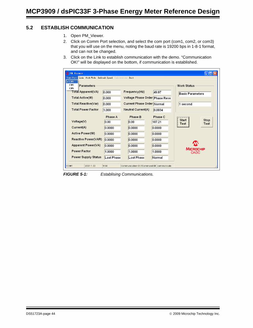
5.2 ESTABLISH COMMUNICATION1. Open PM_Viewer.2. Click on Comm Port selection, and select the com port (com1, com2, or com3)
that you will use on the menu, noting the baud rate is 19200 bps in 1-8-1 format, and can not be changed.
3. Click on the Link to establish communication with the demo. “Communication OK!” will be displayed on the bottom, if communication is established.
FIGURE 5-1: Establising Communications.
DS51723A-page 44 © 2009 Microchip Technology Inc.
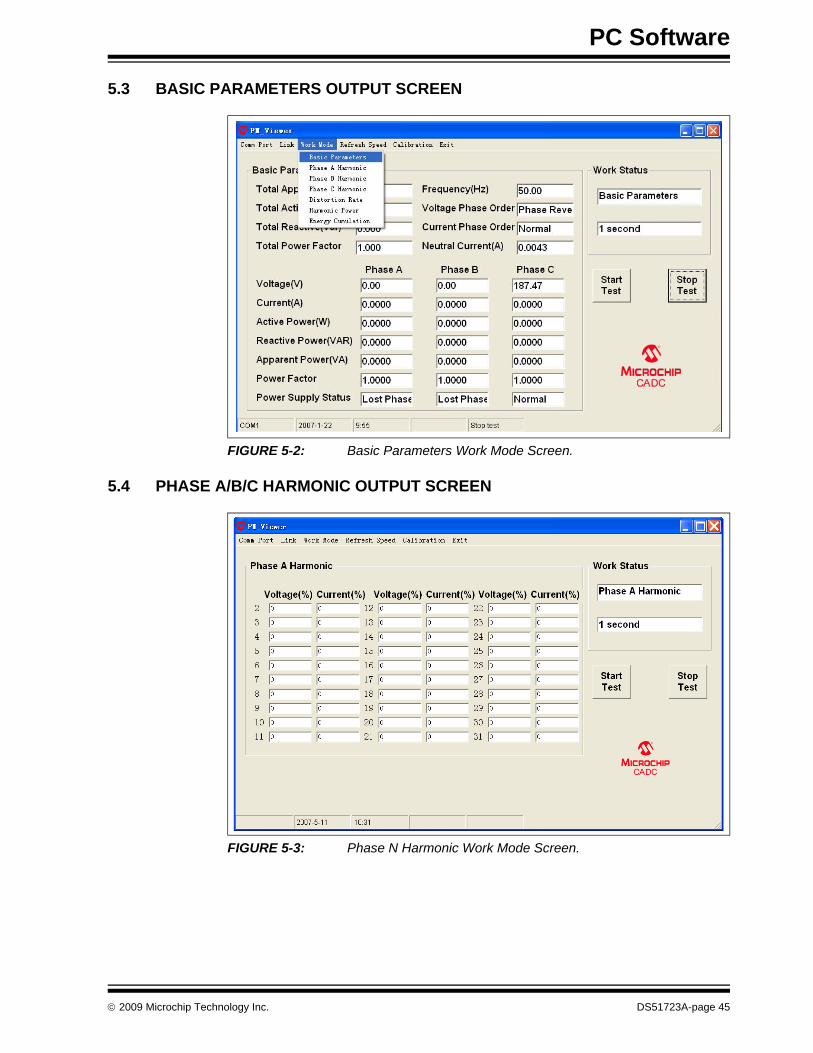
PC Software
5.3 BASIC PARAMETERS OUTPUT SCREEN
FIGURE 5-2: Basic Parameters Work Mode Screen.
5.4 PHASE A/B/C HARMONIC OUTPUT SCREEN
FIGURE 5-3: Phase N Harmonic Work Mode Screen.
© 2009 Microchip Technology Inc. DS51723A-page 45
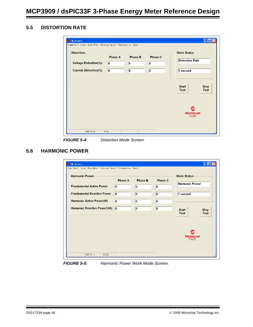
MCP3909 / dsPIC33F 3-Phase Energy Meter Reference Design
5.5 DISTORTION RATE
FIGURE 5-4: Distortion Mode Screen.
5.6 HARMONIC POWER
FIGURE 5-5: Harmonic Power Work Mode Screen.
DS51723A-page 46 © 2009 Microchip Technology Inc.
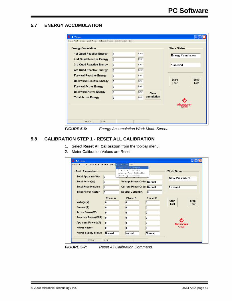
PC Software
5.7 ENERGY ACCUMULATION
FIGURE 5-6: Energy Accumulation Work Mode Screen.
5.8 CALIBRATION STEP 1 - RESET ALL CALIBRATION1. Select Reset All Calibration from the toolbar menu.2. Meter Calibration Values are Reset.
FIGURE 5-7: Reset All Calibration Command.
© 2009 Microchip Technology Inc. DS51723A-page 47
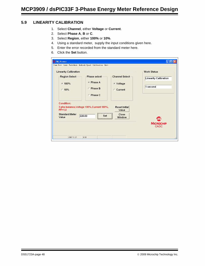
MCP3909 / dsPIC33F 3-Phase Energy Meter Reference Design
5.9 LINEARITY CALIBRATION1. Select Channel, either Voltage or Current.2. Select Phase A, B or C.3. Select Region, either 100% or 10%.4. Using a standard meter, supply the input conditions given here.5. Enter the error recorded from the standard meter here.6. Click the Set button.
DS51723A-page 48 © 2009 Microchip Technology Inc.
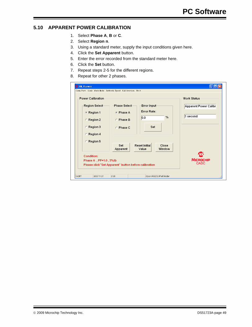
PC Software
5.10 APPARENT POWER CALIBRATION1. Select Phase A, B or C.2. Select Region n.3. Using a standard meter, supply the input conditions given here.4. Click the Set Apparent button.5. Enter the error recorded from the standard meter here.6. Click the Set button.7. Repeat steps 2-5 for the different regions.8. Repeat for other 2 phases.
© 2009 Microchip Technology Inc. DS51723A-page 49

MCP3909 / dsPIC33F 3-Phase Energy Meter Reference Design
5.11 PHASE LAG CALIBRATION1. Select Phase A, B or C.2. Select Region n.3. Using a standard meter, supply the input conditions given here.4. Enter the error recorded from the standard meter here.5. Click the Set button.6. Repeat steps 2-5 for the different regions.7. Repeat for other 2 phases.
DS51723A-page 50 © 2009 Microchip Technology Inc.
MCP3909 / DSPIC33F 3-PHASEENERGY METER REFERENCE DESIGN
Chapter 6. Meter Communications Protocol
6.1 INTRODUCTIONThe UART interface is used to communicate with the upper computer (MCU or PC). Via the UART interface, the upper computer reads the measured parameters of the power grid, and may also send system parameters and calibration parameters to target board as well.The communication interface is a bidirectional interface based on UART, using master/slave half-duplex mode. The baud rate is 19,200 bps, with 1 start bit, 8 data bits and 1 stop bit. Communication is done by frames with non-fixed-length frame structure, definition of which is shonw in Table 6-1. Communication protocol is specified in master-slave structure. The system in this design is the slave, and the upper computer is the master. The master sends commands to the slave, and the slave responds to the master.UART communication uses half-duplex mode. The data format is 8-1-1 and the rate is 19,200 bps. The PC is the host computer, and the target board is the slave.There are 14 command strings that the meter uses. These command strings are defined in Table 6-1
TABLE 6-1: COMMAND STRINGSCommand Description Command
Test Connection 0x41Total Data Request 0x42Harmonic Content, Phase A 0x43Harmonic Content, Phase B 0x44Harmonic Content, Phase C 0x45Total Harmonic Distortion 0x46Energy 0x47Stop Energy Measurement and Clear Energy Values 0x48Harmonic Power 0x49Write Calibration Values to Meter 0x62Write Phase Lag Calibration Values to Meter 0x63Write Power Calibration Values to Meter 0x64Write Energy Pulse Configuration - Active/Apparent 0x65Reset All Calibration Values 0x66Write Energy Pulse Constant 0x67
© 2009 Microchip Technology Inc. DS51723A-page 51
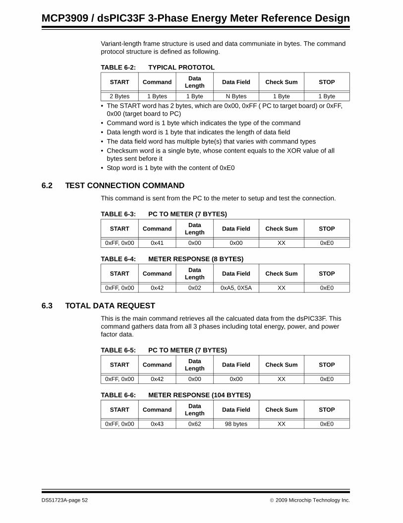
MCP3909 / dsPIC33F 3-Phase Energy Meter Reference Design
Variant-length frame structure is used and data communiate in bytes. The command protocol structure is defined as following.
TABLE 6-2: TYPICAL PROTOTOL
• The START word has 2 bytes, which are 0x00, 0xFF ( PC to target board) or 0xFF, 0x00 (target board to PC)
• Command word is 1 byte which indicates the type of the command• Data length word is 1 byte that indicates the length of data field• The data field word has multiple byte(s) that varies with command types• Checksum word is a single byte, whose content equals to the XOR value of all
bytes sent before it• Stop word is 1 byte with the content of 0xE0
6.2 TEST CONNECTION COMMANDThis command is sent from the PC to the meter to setup and test the connection.
TABLE 6-3: PC TO METER (7 BYTES)
TABLE 6-4: METER RESPONSE (8 BYTES)
6.3 TOTAL DATA REQUESTThis is the main command retrieves all the calcuated data from the dsPIC33F. This command gathers data from all 3 phases including total energy, power, and power factor data.
TABLE 6-5: PC TO METER (7 BYTES)
TABLE 6-6: METER RESPONSE (104 BYTES)
START Command Data Length Data Field Check Sum STOP
2 Bytes 1 Bytes 1 Byte N Bytes 1 Byte 1 Byte
START Command Data Length Data Field Check Sum STOP
0xFF, 0x00 0x41 0x00 0x00 XX 0xE0
START Command Data Length Data Field Check Sum STOP
0xFF, 0x00 0x42 0x02 0xA5, 0X5A XX 0xE0
START Command Data Length Data Field Check Sum STOP
0xFF, 0x00 0x42 0x00 0x00 XX 0xE0
START Command Data Length Data Field Check Sum STOP
0xFF, 0x00 0x43 0x62 98 bytes XX 0xE0
DS51723A-page 52 © 2009 Microchip Technology Inc.
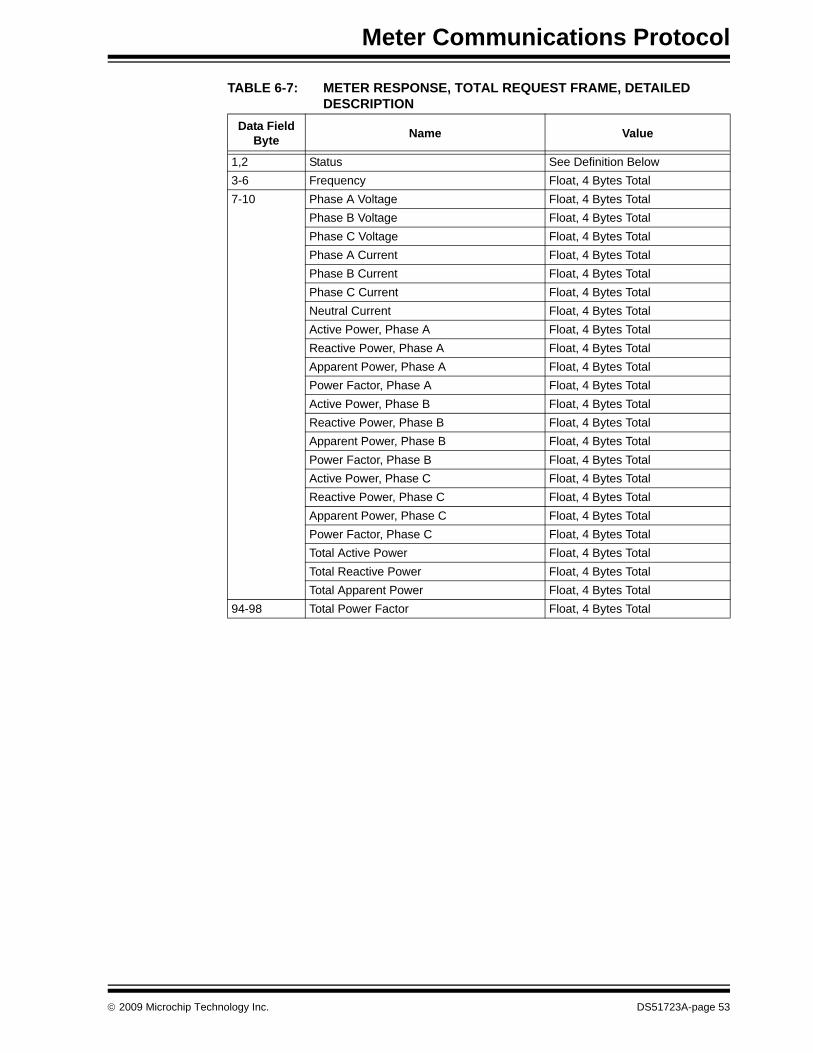
Meter Communications Protocol
TABLE 6-7: METER RESPONSE, TOTAL REQUEST FRAME, DETAILED DESCRIPTION
Data Field Byte Name Value
1,2 Status See Definition Below3-6 Frequency Float, 4 Bytes Total7-10 Phase A Voltage Float, 4 Bytes Total
Phase B Voltage Float, 4 Bytes TotalPhase C Voltage Float, 4 Bytes TotalPhase A Current Float, 4 Bytes TotalPhase B Current Float, 4 Bytes TotalPhase C Current Float, 4 Bytes TotalNeutral Current Float, 4 Bytes TotalActive Power, Phase A Float, 4 Bytes TotalReactive Power, Phase A Float, 4 Bytes TotalApparent Power, Phase A Float, 4 Bytes TotalPower Factor, Phase A Float, 4 Bytes TotalActive Power, Phase B Float, 4 Bytes TotalReactive Power, Phase B Float, 4 Bytes TotalApparent Power, Phase B Float, 4 Bytes TotalPower Factor, Phase B Float, 4 Bytes TotalActive Power, Phase C Float, 4 Bytes TotalReactive Power, Phase C Float, 4 Bytes TotalApparent Power, Phase C Float, 4 Bytes TotalPower Factor, Phase C Float, 4 Bytes TotalTotal Active Power Float, 4 Bytes TotalTotal Reactive Power Float, 4 Bytes TotalTotal Apparent Power Float, 4 Bytes Total
94-98 Total Power Factor Float, 4 Bytes Total
© 2009 Microchip Technology Inc. DS51723A-page 53
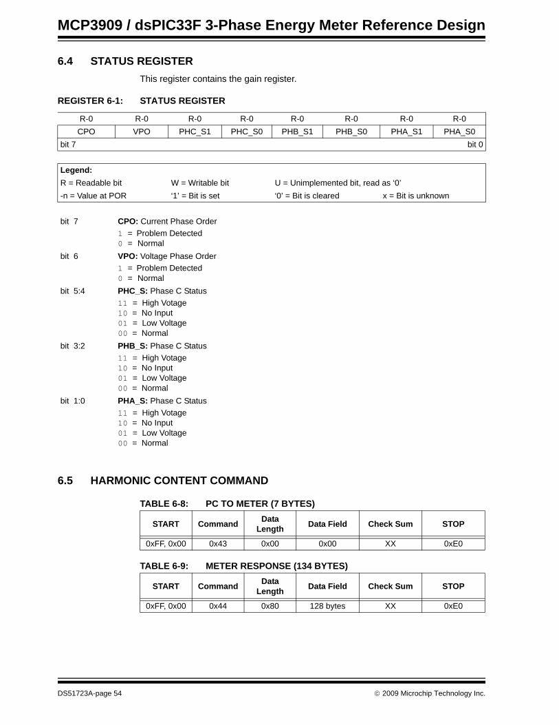
MCP3909 / dsPIC33F 3-Phase Energy Meter Reference Design
6.4 STATUS REGISTERThis register contains the gain register.
REGISTER 6-1: STATUS REGISTER
6.5 HARMONIC CONTENT COMMAND
TABLE 6-8: PC TO METER (7 BYTES)
TABLE 6-9: METER RESPONSE (134 BYTES)
R-0 R-0 R-0 R-0 R-0 R-0 R-0 R-0CPO VPO PHC_S1 PHC_S0 PHB_S1 PHB_S0 PHA_S1 PHA_S0
bit 7 bit 0
Legend:R = Readable bit W = Writable bit U = Unimplemented bit, read as ‘0’-n = Value at POR ‘1’ = Bit is set ‘0’ = Bit is cleared x = Bit is unknown
bit 7 CPO: Current Phase Order 1 = Problem Detected0 = Normal
bit 6 VPO: Voltage Phase Order 1 = Problem Detected0 = Normal
bit 5:4 PHC_S: Phase C Status11 = High Votage10 = No Input01 = Low Voltage00 = Normal
bit 3:2 PHB_S: Phase C Status11 = High Votage10 = No Input01 = Low Voltage00 = Normal
bit 1:0 PHA_S: Phase C Status11 = High Votage10 = No Input01 = Low Voltage00 = Normal
START Command Data Length Data Field Check Sum STOP
0xFF, 0x00 0x43 0x00 0x00 XX 0xE0
START Command Data Length Data Field Check Sum STOP
0xFF, 0x00 0x44 0x80 128 bytes XX 0xE0
DS51723A-page 54 © 2009 Microchip Technology Inc.
Meter Communications Protocol
TABLE 6-10: HARMONIC ANALYSIS DETAILED DESCRIPTION
6.6 TOTAL HARMONIC DISTORTION (THD) COMMAND
TABLE 6-11: PC TO METER (7 BYTES)
TABLE 6-12: METER RESPONSE (29 BYTES)
TABLE 6-13: TOTAL HARMONIC DISTORTION DESCRIPTION
Data Field Byte Description Value
1,2 Fundamential or 1st Harmonic, Voltage Content Unsigned Int, 2 bytes3,4 2nd Harmonic, Voltage Content Unsigned Int, 2 bytes5-56 3-31st Harmonic, Voltage Content Unsigned Int, 2 bytes57,58 Total Voltage Harmonic Content (not including
Fundamental) Unsigned Int, 2 bytes, / 1000 * (100%)
59,60 Fundamential or 1st Harmonic, Current Content Unsigned Int, 2 bytes61,62 2nd Harmonic, Current Content Unsigned Int, 2 bytes63-126 3-31st Harmonic, Current Content Unsigned Int, 2 bytes127,128 Total Current Harmonic Content (not including
Fundamental) Unsigned Int, 2 bytes, / 1000 * (100%)
START Command Data Length Data Field Check Sum STOP
0xFF, 0x00 0x46 0x00 0x00 XX 0xE0
START Command Data Length Data Field Check Sum STOP
0xFF, 0x00 0x47 0x18 24 bytes XX 0xE0
Data Field Byte Description Value
1-4 Total Harmonic Distortion of Phase A Voltage Float, 4 Bytes Total5-8 Total Harmonic Distortion of Phase B Voltage Float, 4 Bytes Total9-12 Total Harmonic Distortion of Phase C Voltage Float, 4 Bytes Total13-16 Total Harmonic Distortion of Phase A Current Float, 4 Bytes Total17-20 Total Harmonic Distortion of Phase B Current Float, 4 Bytes Total21-24 Total Harmonic Distortion of Phase C Current Float, 4 Bytes Total
© 2009 Microchip Technology Inc. DS51723A-page 55

MCP3909 / dsPIC33F 3-Phase Energy Meter Reference Design
6.7 START ENERGY MEASUREMENT COMMAND
TABLE 6-14: PC TO METER (7 BYTES)
TABLE 6-15: METER RESPONSE (42 BYTES)
TABLE 6-16: TOTAL HARMONIC DISTORTION DESCRIPTION
6.8 STOP ENERGY MEASUREMENT COMMAND
TABLE 6-17: PC TO METER (7 BYTES)
TABLE 6-18: METER RESPONSE (7 BYTES)
START Command Data Length Data Field Check Sum STOP
0xFF, 0x00 0x47 0x00 0x00 XX 0xE0
START Command Data Length Data Field Check Sum STOP
0xFF, 0x00 0x48 0x24 36 bytes XX 0xE0
Data Field Byte Description Value
1-4 First quadrant reactive energy Float, 4 Bytes Total5-8 Second quadrant reactive energy Float, 4 Bytes Total9-12 Third quadrant reactive energy Float, 4 Bytes Total13-16 Fouth quadrant reactive energy Float, 4 Bytes Total17-20 Forward Reactive energy Float, 4 Bytes Total21-24 Reverse Reactive Energy Float, 4 Bytes Total25-28 Forward Active Energy Float, 4 Bytes Total29-32 Reverse Active Energy Float, 4 Bytes Total33-36 Reverse Active Energy Float, 4 Bytes Total
START Command Data Length Data Field Check Sum STOP
0xFF, 0x00 0x48 0x00 0x00 XX 0xE0
START Command Data Length Data Field Check Sum STOP
0xFF, 0x00 0x49 0x00 0 bytes XX 0xE0
DS51723A-page 56 © 2009 Microchip Technology Inc.
Meter Communications Protocol
6.9 HARMONIC POWER COMMAND
TABLE 6-19: PC TO METER (7 BYTES)
TABLE 6-20: METER RESPONSE (54 BYTES)
TABLE 6-21: HARMONIC POWER MEASUREMENTS
START Command Data Length Data Field Check Sum STOP
0xFF, 0x00 0x49 0x00 0x00 XX 0xE0
START Command Data Length Data Field Check Sum STOP
0xFF, 0x00 0x4A 0x30 48 bytes XX 0xE0
Data Field Byte Description Value
1-4 Fundamental Active Power Of Phase A Float, 4 Bytes Total5-8 Fundamental Reactive Power Of Phase A Float, 4 Bytes Total9-12 Fundamental Active Power Of Phase B Float, 4 Bytes Total13-16 Fundamental Reactive Power Of Phase B Float, 4 Bytes Total17-20 Fundamental Active Power Of Phase C Float, 4 Bytes Total21-24 Fundamental Reactive Power Of Phase C Float, 4 Bytes Total25-28 Harmonic Active Power Of Phase A Float, 4 Bytes Total29-32 Harmonic Reactive Power Of Phase A Float, 4 Bytes Total33-36 Harmonic Active Power Of Phase B Float, 4 Bytes Total37-40 Harmonic Reactive Power Of Phase B Float, 4 Bytes Total41-44 Harmonic Active Power Of Phase C Float, 4 Bytes Total45-48 Harmonic Reactive Power Of Phase C Float, 4 Bytes Total
© 2009 Microchip Technology Inc. DS51723A-page 57
MCP3909 / dsPIC33F 3-Phase Energy Meter Reference Design
6.10 CALIBRATE METER VOLTAGE/CURRENT COMMAND
TABLE 6-22: PC TO METER (7 BYTES)
TABLE 6-23: METER RESPONSE (7 BYTES)
TABLE 6-24: CALIBRATION OF GAIN AND OFFSET VALUES
START Command Data Length Data Field Check Sum STOP
0xFF, 0x00 0x63 7 0x07 XX 0xE0
START Command Data Length Data Field Check Sum STOP
0xFF, 0x00 0x64 0 0x00 XX 0xE0
Data Field Byte Description Value
1 Phase Select 0x01 = Phase A0x02 = Phase B0x03 = Phase C
2 Range Select 0x01 = 10%0x02 = 100%
3 Channel Select 0x00 = Current0x01 = Voltage
4-7 Correction Factor (Error Being Calibrated Out) Float, 4 Bytes Total
DS51723A-page 58 © 2009 Microchip Technology Inc.
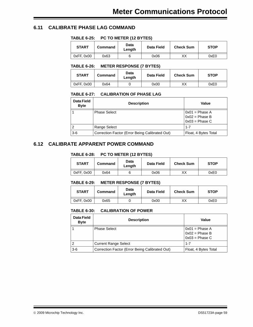
Meter Communications Protocol
6.11 CALIBRATE PHASE LAG COMMAND
TABLE 6-25: PC TO METER (12 BYTES)
TABLE 6-26: METER RESPONSE (7 BYTES)
TABLE 6-27: CALIBRATION OF PHASE LAG
6.12 CALIBRATE APPARENT POWER COMMAND
TABLE 6-28: PC TO METER (12 BYTES)
TABLE 6-29: METER RESPONSE (7 BYTES)
TABLE 6-30: CALIBRATION OF POWER
START Command Data Length Data Field Check Sum STOP
0xFF, 0x00 0x63 6 0x06 XX 0xE0
START Command Data Length Data Field Check Sum STOP
0xFF, 0x00 0x64 0 0x00 XX 0xE0
Data Field Byte Description Value
1 Phase Select 0x01 = Phase A0x02 = Phase B0x03 = Phase C
2 Range Select 1-73-6 Correction Factor (Error Being Calibrated Out) Float, 4 Bytes Total
START Command Data Length Data Field Check Sum STOP
0xFF, 0x00 0x64 6 0x06 XX 0xE0
START Command Data Length Data Field Check Sum STOP
0xFF, 0x00 0x65 0 0x00 XX 0xE0
Data Field Byte Description Value
1 Phase Select 0x01 = Phase A0x02 = Phase B0x03 = Phase C
2 Current Range Select 1-73-6 Correction Factor (Error Being Calibrated Out) Float, 4 Bytes Total
© 2009 Microchip Technology Inc. DS51723A-page 59
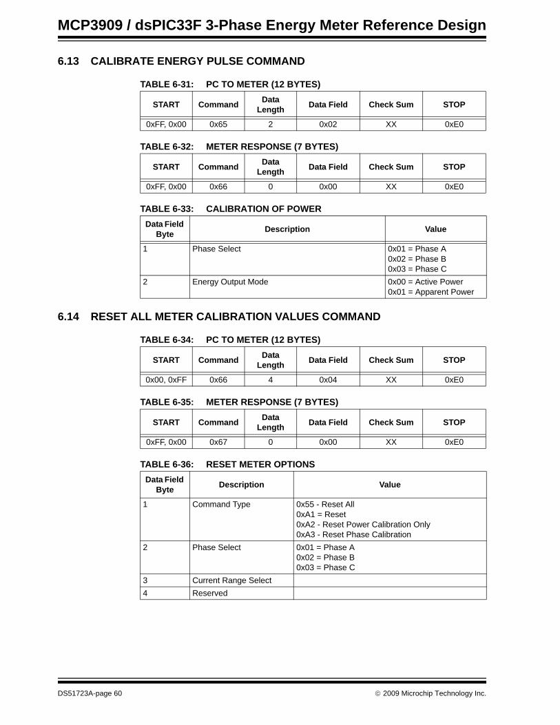
MCP3909 / dsPIC33F 3-Phase Energy Meter Reference Design
6.13 CALIBRATE ENERGY PULSE COMMAND
TABLE 6-31: PC TO METER (12 BYTES)
TABLE 6-32: METER RESPONSE (7 BYTES)
TABLE 6-33: CALIBRATION OF POWER
6.14 RESET ALL METER CALIBRATION VALUES COMMAND
TABLE 6-34: PC TO METER (12 BYTES)
TABLE 6-35: METER RESPONSE (7 BYTES)
TABLE 6-36: RESET METER OPTIONS
START Command Data Length Data Field Check Sum STOP
0xFF, 0x00 0x65 2 0x02 XX 0xE0
START Command Data Length Data Field Check Sum STOP
0xFF, 0x00 0x66 0 0x00 XX 0xE0
Data Field Byte Description Value
1 Phase Select 0x01 = Phase A0x02 = Phase B0x03 = Phase C
2 Energy Output Mode 0x00 = Active Power0x01 = Apparent Power
START Command Data Length Data Field Check Sum STOP
0x00, 0xFF 0x66 4 0x04 XX 0xE0
START Command Data Length Data Field Check Sum STOP
0xFF, 0x00 0x67 0 0x00 XX 0xE0
Data Field Byte Description Value
1 Command Type 0x55 - Reset All0xA1 = Reset0xA2 - Reset Power Calibration Only0xA3 - Reset Phase Calibration
2 Phase Select 0x01 = Phase A0x02 = Phase B0x03 = Phase C
3 Current Range Select4 Reserved
DS51723A-page 60 © 2009 Microchip Technology Inc.

Meter Communications Protocol
6.15 CALIBRATE METER CONSTANT (ENERGY PULSE OUTPUT CONSTANT)
TABLE 6-37: PC TO METER (9 BYTES)
TABLE 6-38: METER RESPONSE (7 BYTES)
TABLE 6-39: ENERGY CONSTANT OPTIONS OPTIONS
START Command Data Length Data Field Check Sum STOP
0x00, 0xFF 0x67 2 0x02 XX 0xE0
START Command Data Length Data Field Check Sum STOP
0xFF, 0x00 0x68 0 0x00 XX 0xE0
Data Field Byte Description Value
1-2 Energy Constant Range of 10064000 (Decimal)
© 2009 Microchip Technology Inc. DS51723A-page 61

MCP3909 / dsPIC33F 3-Phase Energy Meter Reference Design
NOTES:
DS51723A-page 62 © 2009 Microchip Technology Inc.

MCP3909 / DSPIC33F 3-PHASEENERGY METER REFERENCE DESIGN
Appendix A. Schematics and Layouts
A.1 INTRODUCTIONThis appendix contains the following schematics and layouts for the MCP3909 / dsPIC33F 3-Phase Energy Meter Reference Design.• Power Supply Board Schematic• Main Board Schematic - Page 1• Main Board Schematic - Page 2• Power Supply Board - Assembly Drawing• Power Supply Board - Composite Drawing• Main Board - Assembly Drawing• Main Board - Composite Drawing
A.2 SCHEMATICS AND PCB LAYOUT
FIGURE A-1: LAYER ORDER
Top Layer
Bottom Layer
© 2009 Microchip Technology Inc. DS51723A-page 63

MCP3909 / dsPIC33F 3-Phase Energy Meter Reference Design
FIGURE A-2: POWER SUPPLY BOARD SCHEMATIC
12
34
ABCD
43
21
D C B ATi
tle
Num
ber
Revi
sion
Size A4
Dat
e:30
-Nov
-200
7Sh
eet
of
File
:X
:\AIP
D E
val B
oard
s\102
-000
11 th
ru 0
0020
\102
-000
18\P
CB F
iles (
Prot
el )\
PCB-
R5\P
M33
_D
raw
n By
:
R2 150k
R7 150k
R11
150k
1
JP51
JP41
JP1
thre
e ph
ase
volta
ge in
put
N
T3SP
T204
B
T1SP
T204
B
T2SP
T204
B
2R =
Vou
r*Ri
n/(K
pt*V
in)
1
JP6
Pow
er su
pply
for
3phs
pow
er m
eter
2.0
1 - 1
NNPA PB PC
N1
C2
B3
A4
G1
5
Vo1
6
G2
7
Vo2
8T4 D
B-12
CY
RV3
RV1
RV2
A1
B2
C3
N4
N5
C6
B7
A8
R5 COIL
S
12V
PC
C7 33N
R10
1K 1
%
N
PC-
PC-
PC+
PB-
PB+
PA-
PA+
R12 0
PA+
PA-
PB+
PB-
PC+
PC-
1 2 3 4 5 6 7 8 9 10
JP3
Hea
der 1
0
R9 499K
1%
PB
C5 33N
PB-
PA
C3 33N
PA-
W1
Jum
per
C4 0.1u
C1 0.1U
C6 0.1u
PA PB PC N
N N N
PAPBPCN
R8 499K
1%
R4 499K
1%
R3 499K
1%
R13
499K
1%
R14
499K
1%
R6 1K 1
%
R1 1K 1
%
N
W2
Jum
per
W3
Jum
per
1 2 3
JP6
Hea
der 3
+C2 10
0uf
DS51723A-page 64 © 2009 Microchip Technology Inc.
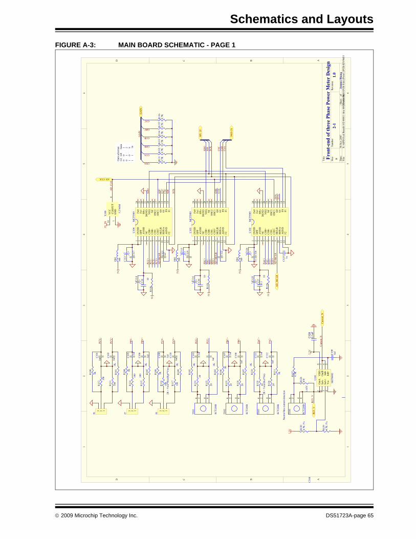
Schematics and Layouts
FIGURE A-3: MAIN BOARD SCHEMATIC - PAGE 1
12
34
56
ABCD
65
43
21
D C B A
Title
Num
ber
Rev
ision
Size B Dat
e:30
-Nov
-200
7Sh
eet
of
File
:X
:\AIP
D E
val B
oard
s\102
-000
11 th
ru 0
0020
\102
-000
18\P
CB
File
s (Pr
otel
)\PC
B-R
5\PM
33_
Dra
wn
By:
Fron
t-end
of t
hree
Pha
se P
ower
Met
er D
esig
n1.
0
R11
3
100
R10
2
1K
R10
0
1KC
101
1nf
C10
4
1nf
R11
2 100
R12
1
20
R10
11K
C10
2
1nf
R12
2
20
C10
3 1nf
R10
31K
R11
510
0 R10
6 1K
R10
4 1KC
105 1nf
C10
8
1nf
R11
4
100
R12
3
20
R10
51K
C10
6
1nf
R12
4
20
C10
7 1nf
R10
7
R11
7
100
R11
01K
R10
8
1KC
109
1nf
C11
2
1nf
R11
6
100
R12
5
20
R10
91K
C11
0
1nf
R12
6
20
C11
1 1nf
R11
1
1K
2R =
Vou
r*R
in/(K
pt*V
in)
2R =
Vou
t/(K
ct*I
in)
426 8
T101
SCT2
20B
426 8
T102
SCT2
20B
426 8
T103
SCT2
20B
426 8
T100
SCT2
20B
Cur
rent
_N
R12
847
0
R12
74.
7K
C10
01n
f
Neu
tral l
ine
curre
nt d
etec
tion
3.3V
C12
80.
1uF
R13
04.
7K 1
%
R12
94.
7K 1
%
3.3V
PCV
-
PCV
+
PCC
+
PCC
-
PBV
-
PBV
+
PBC
+
PBC
-
PAV
-
PAV
+
PAC
+
PAC
-
Cur
rent
_N
1.65
V
C12
11u
f
C12
3 1u
5V_I
N
C12
2
AD
_MCL
R
5V
5V
5V
5V
5V
5V
C12
60.
1C
127
0.1
C11
7
C11
8
C11
9
C12
0
VC
C14
GN
D7
CLK
OU
T8
X10
0 3.27
68M
Gai
n se
lect
ion
G1
G0
G
ain
0
0
10
1
2
1
0
81
1
1
6
+C11
4
+
C11
3
+C11
6
+C11
5
+C12
5+C
124
DV
DD
1
HPF
2
AV
DD
3
NC
4
CH
0+5
CH
0-6
CH
1_7
CH
1+8
MCL
R9
REF
i/o10
AG
ND
11
F212
F113
F014
G1
15G
016
OSC
117
OSC
218
NC
19N
EG20
DG
ND
21H
Fo22
Fo1
23Fo
024
U10
2M
CP3
909
DV
DD
1
HPF
2
AV
DD
3
NC
4
CH
0+5
CH
0-6
CH
1_7
CH
1+8
MCL
R9
REF
i/o10
AG
ND
11
F212
F113
F014
G1
15G
016
OSC
117
OSC
218
NC
19N
EG20
DG
ND
21H
Fo22
Fo1
23Fo
024
U10
3M
CP3
909
DV
DD
1
HPF
2
AV
DD
3
NC
4
CH
0+5
CH
0-6
CH
1_7
CH
1+8
MCL
R9
REF
i/o10
AG
ND
11
F212
F113
F014
G1
15G
016
OSC
117
OSC
218
NC
19N
EG20
DG
ND
21H
Fo22
Fo1
23Fo
024
U10
4M
CP3
909
R13
14.
7K
R13
24.
7K
R13
34.
7K
R13
44.
7K
R13
54.
7K
R13
64.
7K
G0A
G1A
G0B
G1B
G0C
G1C
PCC
+PC
C-
PCV
-PC
V+
AD
MCL
R
PBC
+PB
C-
PBV
-PB
V+
PAC
+PA
C-
PAV
-PA
V+
AD
MCL
R
GA
IN
G0A
G1A
SDI
SCK
G0B
G1B
G0C
G1C
GA
IN
CSC
CSB
CSA
3905
CS
SDO
SPI
I/F
AD
_CLK
REF
_VRE
V_V
AD_CLK
2-1
Jem
mey
Hua
ng
123
J6
123
J7
123
J8
FB3
500
FB2
500
AD
_MCL
R
FB1
500
R11
810
R11
910
R12
010
Out
A1
InA
-2
InA
+3
Vss
4In
B+
5In
B-
6O
utB
7V
DD
8U
101
MC
P600
2
CSC
SDI
SCK
SDO
© 2009 Microchip Technology Inc. DS51723A-page 65
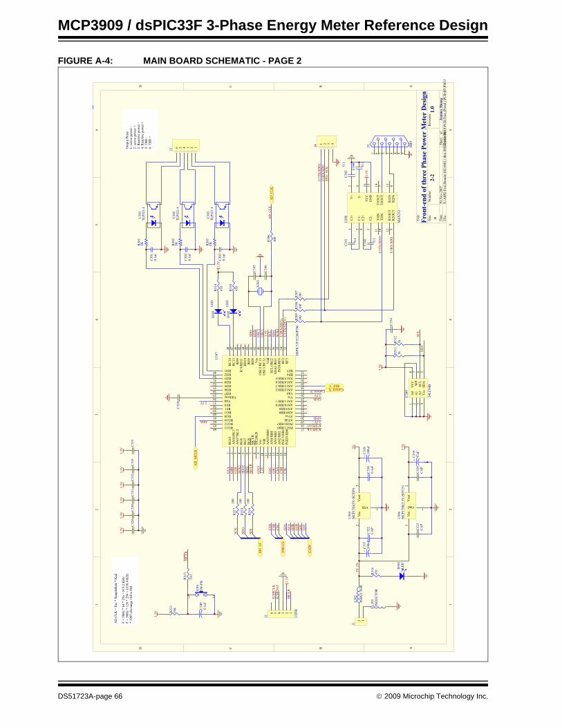
MCP3909 / dsPIC33F 3-Phase Energy Meter Reference Design
FIGURE A-4: MAIN BOARD SCHEMATIC - PAGE 2
12
34
56
ABCD
65
43
21
D C B A
Title
Num
ber
Rev
ision
Size B Dat
e:30
-Nov
-200
7Sh
eet
of
File
:X
:\AIP
D E
val B
oard
s\102
-000
11 th
ru 0
0020
\102
-000
18\P
CB
File
s (Pr
otel
)\PC
B-R
5\PM
33D
raw
n By
:
R31
3
510
C34
00.
1uf
11 2 2
S301
SW-P
B 3.3V
3.3V
Jem
mey
Hua
ng
Fron
t-end
of t
hree
Pha
se P
ower
Met
er D
esig
n1.
0
AD
CLK
= F
ac *
Sam
pleR
ate
* K
ad
F =
50H
z *
64 *
256
= 8
19.2
KH
zF
= 50
Hz
* 12
8 *
256
= 16
38.4
KH
z*
3905
clk
rang
e 1M
to 4
MC
328
123456
J2 CO
N6
3.3V
C33
0
3.3V
C33
1
3.3V
C33
2
3.3V
C33
3
C33
4
R32
110
k
ICSP
DA
TIC
SPC
LK
MCL
R
3.3V
C32
2C
AP
C33
60.
1uF
+C
337
100u
f
5V
C32
3C
AP
C32
4C
AP
+C
338
100u
f
+C
339
47uF
D30
1LE
D
R31
647
0
A0
1
A1
2
A2
3
Vss
4SD
A5
SCL
6W
P7
VC
C8
U30
9
24LC
04B
3.3V
R31
11k
R31
21k
3.3V
C33
5
Vin
3V
out
2
Gnd 1
U30
6M
CP1
700(
3.3V
-SO
T23)
12
J1
123456
J3
C34
2 0.1
C34
1 0.1
C34
4 0.1
C34
30.
1
C1+
1V
+2
C1-
3
C2-
5
T2O
UT
7
C2+
4V
-6
R2I
N8
T1IN
11
T2IN
10
R1O
UT
12
R2O
UT
9R
1IN
13
T1O
UT
14
GN
D15
VC
C16
U30
8
MA
X23
2
3.3V
1 6 2 7 3 8 4 9 5
J5 DB
9
U1R
X/S
DI1
U1T
X/S
DO
1
5V_I
N
SCL
SDA
C32
9
RG
151
AN
16/R
C1
2
AN
17/R
C2
3
RG
64
RG
75
RG
86
MCL
R7
SS2/
RG
98
Vss
9
Vdd
10
AN
15/R
B5
11
AN
4/R
B4
12
AN
3/R
B3
13
AN
2/R
B2
14
PGC
3/R
B1
15
PGD
3/R
B0
16
PGC1/RB6 17
PGD1/RB7 18
AVdd 19
AVss 20
AN8/RB8 21
AN9/RB9 22
AN10/RB10 23
AN11/RB11 24
Vss 25
Vdd 26
AN12/RB12 27
AN13/RB13 28
AN14/RB14 29
AN15/RB15 30
RF4 31
RF5 32
RF3
33R
F234
INT0
/RF6
35SD
A1/
RG
336
SCL1
/RG
237
Vdd
38O
SC1/
RC
1239
OSC
2/R
C15
40V
ss41
RD
842
RD
943
RD
1044
IC4/
RD
1145
RD
046
RC
1347
RC
1448
RD149 RD250 RD351 RD452 RD553 RD654 RD755 Vddcore56 Vdd57 RF058 RF159 RG160 RG061 RG1462 RG1263 RG1364
U30
7 DSP
IC33
FJ12
8GP7
06
OSC
1O
SC2
MCL
R
ICSPDATICSPCLK
C34
5
C34
6
X30
3
3.3V
3.3V
GND
GND
GN
D
3.3V
3.3V
GN
D
3.3V
R31
810
0
R31
710
0
R31
910
0
D30
3LE
DR
314
470
3.3V
CSA
G0A
G1A
SCK
SDI
SDO
CSB
G0B
G1B
CSC
G0C
G1C
SPI
I/F
CSA
G0A
G1A
CSB
G0B
G1B
CSC
G0C
G1C
GA
IN
3909
CS
SCL
SDA
U1R
X(S
DI1
)U
1TX
(SD
O1)
Current_NCurrent_N
SDO
3.3V
REF_V
SCK
1
SCK
2SD
O2
SDI2
U1R
X/S
DI1
U1T
X/S
DO
1
SPI1
_SC
K
1 2 3 4
J4
L302
IND
UCT
OR
L301
IND
UCT
OR
R30
31K
C30
30.
1uf
U30
3TL
P521
-1
R30
21K
C30
20.
1uf
U30
2TL
P521
-1
R30
11K
C30
10.
1uf
U30
1TL
P521
-1
D30
2LE
DR
310
470
AD
_CLK
AD
_CLK
Out
put P
ulse
1: a
ctiv
e po
wer
-2:
act
ive
pow
er +
3: R
eact
ive
pow
er -
4: R
eact
ive
pow
er +
5: T
BD -
6: T
BD +
2-2
AD
_MCL
R
MCL
R
R30
910
0R
308
100
R30
710
0
R30
6
100
Vin
2V
out
3
VSS 1
U30
5M
CP1
701(
5V-S
OT8
9)
DS51723A-page 66 © 2009 Microchip Technology Inc.
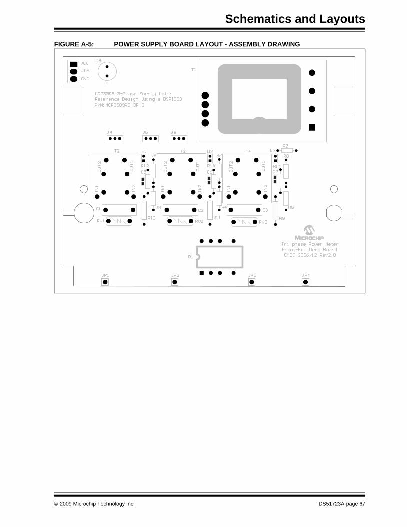
Schematics and Layouts
FIGURE A-5: POWER SUPPLY BOARD LAYOUT - ASSEMBLY DRAWING
© 2009 Microchip Technology Inc. DS51723A-page 67
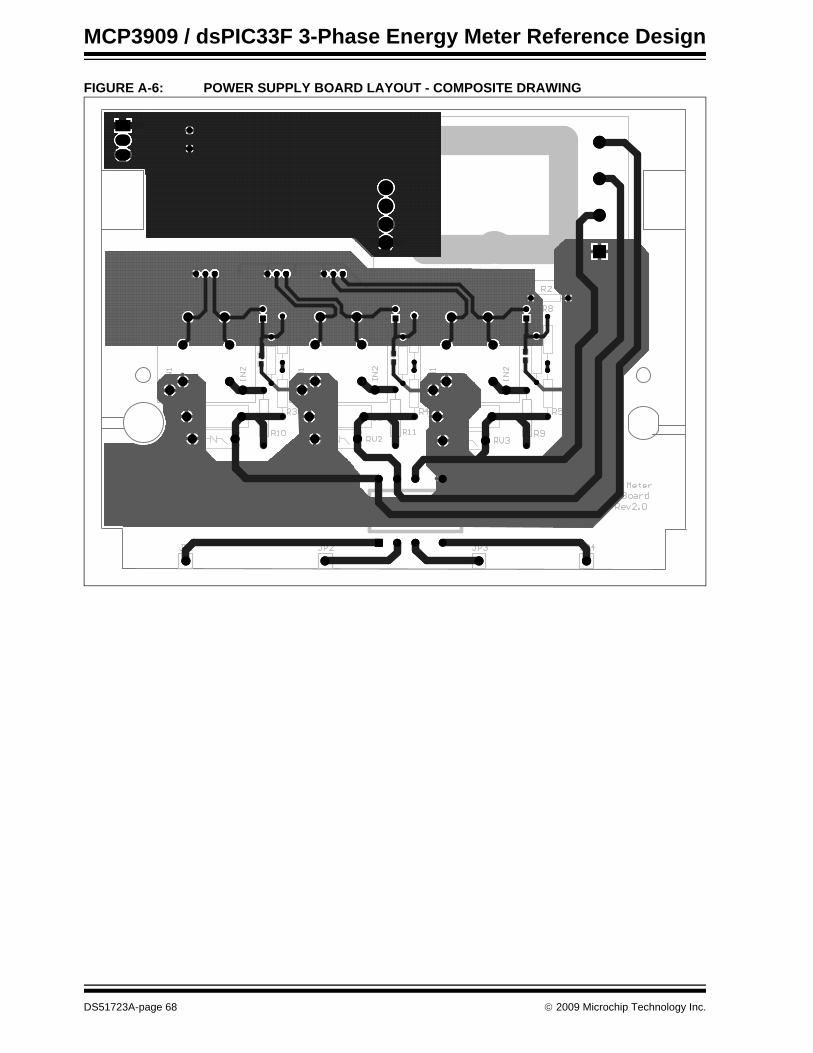
MCP3909 / dsPIC33F 3-Phase Energy Meter Reference Design
FIGURE A-6: POWER SUPPLY BOARD LAYOUT - COMPOSITE DRAWING
DS51723A-page 68 © 2009 Microchip Technology Inc.
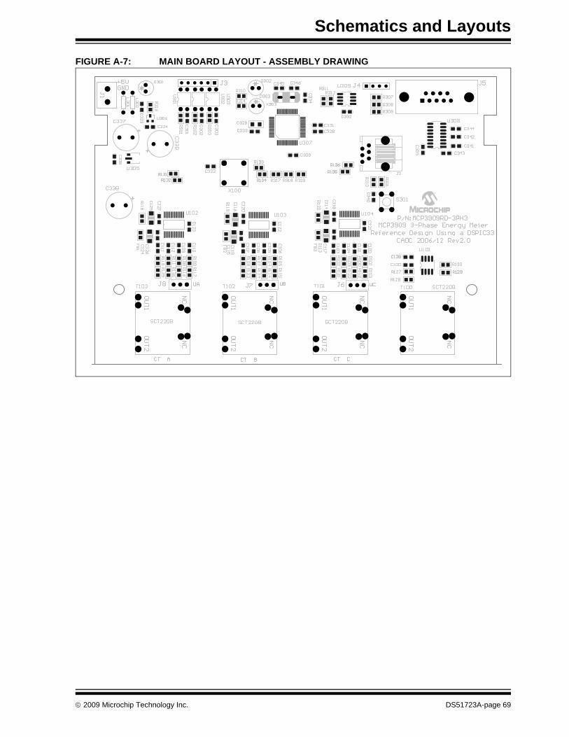
Schematics and Layouts
FIGURE A-7: MAIN BOARD LAYOUT - ASSEMBLY DRAWING
© 2009 Microchip Technology Inc. DS51723A-page 69
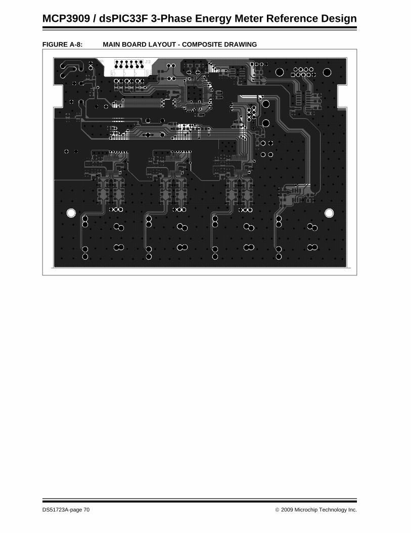
MCP3909 / dsPIC33F 3-Phase Energy Meter Reference Design
FIGURE A-8: MAIN BOARD LAYOUT - COMPOSITE DRAWING
DS51723A-page 70 © 2009 Microchip Technology Inc.

MCP3909 / DSPIC33F 3-PHASEENERGY METER REFERENCE DESIGN
Appendix B. Bill Of Materials (BOM)
TABLE B-1: BILL OF MATERIALS - POWER SUPPLY (BOTTOM BOARD)
Qty Reference Description Manufacturer Part Number3 C1, C2, C3 CAP 0.1UF 305VAC EMI SUPPRESS EPCOS Inc B32922A2104M1 C4 CAP 470UF 25V ALUM LYTIC RADIAL Panasonic® - ECG ECA-1EM4713 C5, C6, C7 DO NOT POPULATE — —3 J4, J5, J6 CONN HEADER 3POS .100 VERT TIN Molex®/Waldom
Electronics Corp22-23-2031
4 JP1, JP2, JP3, JP4
HOOK-UP WIRE 18AWG STRAND RED Alpha Wire Company
3055 RD005
4 JP1, JP2, JP3, JP4
CONN RING TERM #6 18-22AWG Molex/Waldom Elec-tronics Corp
19070-0040
1 JP6 CONN HEADER 3POS .156 VERT TIN Molex/Waldom Electronics Corp
26-48-1035
1 JP6 CONN HOUSING 3POS .156 W/O RAMP Molex/Waldom Electronics Corp
09-50-7031
3 JP6 CONN TERM FEMALE 18-24AWG TIN Molex/Waldom Electronics Corp
08-50-0105
1 PCB RoHS Compliant Bare PCB, dsPIC33F and MCP3909 3-Phase Energy Meter (Power) Bottom Bd.
Microchip Technology Inc.
104-00158
3 P4, P5, P6 CONN HOUS 3POS .100 W/RAMP/RIB (Connects to Above)
Molex/Waldom Electronics Corp
22-01-3037
9 P4, P5, P6 CRIMP TERM FEMALE 22-30AWG TIN Molex/Waldom Electronics Corp
08-65-0805
1 R1 Part of T1 Sanki —1 R2 DO NOT POPULATE — —6 R3, R4, R5, R6,
R7, R8DO NOT POPULATE — —
3 R9, R10, R11 RES 150K OHM METAL FILM .50W 1% Vishay®/Phoenix Passive Components
5033ED150K0F12AF5
3 R12, R13, R14 DO NOT POPULATE — —3 RV1, RV2, RV3 VARISTOR 300V RMS 14MM RADIAL EPCOS Inc S14K300E21 T1 3P AC-DC converter, 220V - 12V/5V Sanki DB-12CY2203 T2, T3, T4 2mA/2mA Current transformer Xinge SPT2043 W1, W2, W3 DO NOT POPULATE — —Note 1: The components listed in this Bill of Materials are representative of the PCB assembly. The released BOM
used in manufacturing uses all RoHS-compliant components.
© 2009 Microchip Technology Inc. DS51723A-page 71
MCP3909 / dsPIC33F 3-Phase Energy Meter Reference Design
TABLE B-2: BILL OF MATERIALS - TOP BOARD
Qty Reference Description Manufacturer Part Number13 C100, C101, C102,
C103, C104, C105, C106, C107, C108, C109, C110, C111, C112
CAP 1000PF 50V CERAMIC X7R 0805
Kemet® Electronics Corp
C0805C102K5RACTU
6 C113, C114, C115, C116, C124, C125
CAP CER 10UF 16V X7R 1206 Murata Electronics® North America
GRM31CR71C106KAC7L
26 C117, C118, C119, C120, C126, C127, C128, C301, C302, C303, C322, C323, C324, C328, C330, C331, C332, C333, C334, C335, C336, C340, C341, C342, C343, C344
CAP .1UF 25V CERAMIC X7R 0805 Panasonic® - ECG ECJ-2VB1E104K
4 C121, C122, C123, C329
CAP 1.0UF 10V CERAMIC X7R 0805 Kemet Electronics Corp
C0805C105K8RACTU
3 C337, C338, C339 CAP 470UF 25V ALUM LYTIC RADIAL
Panasonic - ECG ECA-1EM471
2 C345, C346 CAP 22PF 50V CERM CHIP 0805 SMD
Panasonic - ECG ECJ-2VC1H220J
3 6" Wire Thru CT HOOK-UP WIRE 16AWG STRAND RED
Alpha Wire Company
3057 RD005
6 CT Wire terminals CONN RING TERM #6 18-22AWG Molex/Waldom Electronics Corp
19070-0040
1 D301 LED 3MM ALGAAS RED CLEAR LITE-ON INC LTL-4266N1 D302 LED 3MM GREEN CLEAR LITE-ON INC LTL-4236N1 D303 LED 3MM YELLOW CLEAR LITE-ON INC LTL-4256N3 FB1, FB2, FB3 FERRITE SMT luying STBL2012-1211 J1 CONN HOUSING 3POS .156 W/O
RAMPMolex/Waldom Electronics Corp
09-50-7031
1 J1 CONN TERM FEMALE 18-24AWG TIN
Molex/Waldom Electronics Corp
08-50-0105
1 J1 HOOK-UP WIRE 22AWG STRAND RED
Alpha Wire Company
3051 RD005
1 J1 HOOK-UP WIRE 22AWG STRAND BLACK
Alpha Wire Company
3051 BK005
1 J2 CONN MOD JACK 6-6 VERT PCB 50AU
Tyco Electronics/Amp
5520258-3
1 J3 CONN HEADER 6POS .100 VERT TIN
Molex/Waldom Electronics Corp
22-27-2061
1 J4 CONN HEADER 4POS .100 VERT TIN
Molex/Waldom Electronics Corp
22-27-2041
1 J5 DB9 Female vertical Tyco Electronics/Amp
747091-2
3 J6,J7 & J8 CONN HOUS 3POS .100 W/RAMP/RIB (Connects to J4,J5 & J6 of Lower Board)
— —
9 J6,J7 & J8 CRIMP TERM FEMALE 22-30AWG TIN
Molex/Waldom Electronics Corp
08-65-0805
Note 1: The components listed in this Bill of Materials are representative of the PCB assembly. The released BOM used in manufacturing uses all RoHS-compliant components.
DS51723A-page 72 © 2009 Microchip Technology Inc.

Bill Of Materials (BOM)
3 J6,J7 & J8 HOOK-UP WIRE 22AWG STRAND GREEN
Alpha Wire Company
3051 GR005
3 J6,J7 & J8 HOOK-UP WIRE 22AWG STRAND RED
Alpha Wire Company
3051 RD005
3 J6,J7 & J8 HOOK-UP WIRE 22AWG STRAND BLACK
Alpha Wire Company
3051 BK005
2 L301, L302 60ohm bead Jones B601 PCB RoHS Compliant Bare PCB,
dsPIC33F and MCP3909 3-Phase Energy Meter (Power) Bottom Bd.
— 104-00159
17 R100, R101, R102, R103, R104, R105, R106, R107, R108, R109, R110, R111, R301, R302, R303, R311, R312
RES 1.00K OHM 1/8W 1% 0805 SMD Panasonic - ECG ERJ-6ENF1001V
12 R112, R113, R114, R115, R116, R117, R307, R308, R309, R317, R318, R319
RES 100 OHM 1/8W 1% 0805 SMD Panasonic - ECG ERJ-6ENF1000V
3 R118, R119, R120 RES 10.0 OHM 1/8W 1% 0805 SMD Panasonic - ECG ERJ-6ENF10R0V6 R121, R122, R123,
R124, R125, R126RES 20.0 OHM 1/8W 1% 0805 SMD Panasonic - ECG ERJ-6ENF20R0V
7 R127, R131, R132, R133, R134, R135, R136
RES 4.7K OHM 1/8W 5% 0805 SMD Panasonic - ECG ERJ-6GEYJ472V
4 R128, R310, R314, R316
RES 470 OHM 1/8W 5% 0805 SMD Panasonic - ECG ERJ-6GEYJ471V
2 R129, R130 RES 4.70K OHM 1/8W 1% 0805 SMD Yageo Corporation 9C08052A4701FKHFT1 R313 RES 510 OHM 1/8W 5% 0805 SMD Panasonic - ECG ERJ-6GEYJ511V1 R321 RES 10.0K OHM 1/8W 1% 0805 SMD Panasonic - ECG ERJ-6ENF1002V1 S301 SWITCH TACT 6MM MOMENTARY
250GF E-Switch TL1105BF250Q
1 X100 3.2768Mhz Crystal Koan DIP-8-3.2768M1 X303 7.3728Mhz Crystal Koan HC-49S-SMD-7.3728M1 U305 2uA Low Dropout Positive Voltage
RegulatorMicrochip Technology Inc
MCP1701T-5002I/MB
1 U306 Low Quiescent Current LDO Microchip Technology Inc
MCP1700T-3302E/TT
1 U307 High-Performance, 16-bit Digital Sig-nal Controllers
Microchip Technology Inc
dsPIC33FJ128GP206
1 U308 IC DRVR/RCVR MULTCH RS232 16SOIC
Texas Instruments MAX3232CDR
1 U309 4K I2C™ Serial EEPROM Microchip Technology Inc
24LC04B-E/SN
3 U102, U103 U104 Energy Metering IC with SPI Interface and Active Power Pulse Output
Microchip Technology Inc
MCP3909-I/SS
1 U101 1MHz, Low Power Op-Amp Microchip Technology Inc
MCP6002-I/SN
3 T101 T102, T103 5A/5mA Current transformer Xinge SCT954F1 T100 " DO NOT POPULATE — —
TABLE B-2: BILL OF MATERIALS - TOP BOARD
Qty Reference Description Manufacturer Part Number
Note 1: The components listed in this Bill of Materials are representative of the PCB assembly. The released BOM used in manufacturing uses all RoHS-compliant components.
© 2009 Microchip Technology Inc. DS51723A-page 73

MCP3909 / dsPIC33F 3-Phase Energy Meter Reference Design
NOTES:
DS51723A-page 74 © 2009 Microchip Technology Inc.

MCP3909 / DSPIC33F 3-PHASEENERGY METER REFERENCE DESIGN
Appendix C. Power Calculation Theory
C.1 OVERVIEWThis MCP3909 / dsPIC33F 3-Phase Energy Meter Reference Design is unique in that all calculations are done in the frequency domain. This is easily realized using the DSP engine core of the advanced 16-bit MCU, the dsPIC33F. In addition to performing direct fourier transforms (DFTs) on all the input channel measurements, an additional firmware function is included, quasi-synchronous sampling.
C.2 SYNCHRONOUS SAMPLING AND QUASI-SYNCHRONOUS SAMPLINGThe fundamentals of quasi-synchronous sampling and corresponding methods for measuring AC electrical parameters are discussed in this section. Typically, a synchronous sampling method is used for measuring electrical parameters. The method requires synchronization between sampling intervals and power grid frequency. For these types of meter designs, an external hardware PLL circuit is used to track power grid frequency, and the clock of the MCP3909 device is automatically updated to change the sampling frequency. Since the PLL output frequency drops behind the power grid frequency, a synchronous error exists in the system, and fully synchronous sampling is hard to achieve. In addition, as non-sine waves exist in the power grid, which may affect zero-crossing detection, when such conditions worsen, it may cause PLL failure, preventing the system from working normally.For the MCP3909 / dsPIC33F 3-Phase Energy Meter Reference Design presented here, the dsPIC33F performs additionall calculations that eliminates the need for a costly external PLL circuit. This quasi-synchronous sampling method has an advantage in the engineering practice, which actually is periodic sampling, without synchronizing with the power grid frequency. Therefore, the zero-crossing detection and PLL circuit can be reduced to lower the hardware complexity. The tradeoff is the increased software requirements of the system, easily realized using the powerful dsPIC33F.For DFT or FFT harmonic analysis of periodic signals, a Fourier transform may only bring accurate spectrum analysis when the sampling points satisfy N > 2M for each line cycle and strict synchronous sampling is realized. (Where M is the maximal harmonic order of periodic signals, and N is the number of samples per line cycle).Otherwise, if N ≤ 2M, it will cause spectrum aliasing. In addition, if strict synchronous sampling cannot be realized, spectral-leakage will occur (the Hurdle Effect). However, in the quasi-synchronous sampling method emplyed here, strict synchronization between sampling intervals and the period of sampled signal is not guaranteed but is overcome through post-processing and iteration of the collected data. To reduce the error caused by this problem and to obtain better accuracy when measuring the fundamental and harmonics of higher orders, an increase in the number of iterations when processing data to improve accuracy is performed.The iterations can effectively reduce the impact of synchronization error over the mea-surement accuracy, and is one of the methods to realize accurate measurement of the frequency and harmonics under steady-state conditions.
© 2009 Microchip Technology Inc. DS51723A-page 75
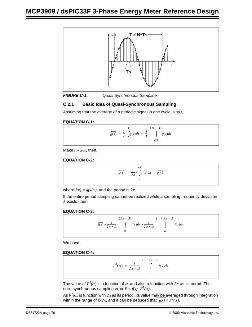
MCP3909 / dsPIC33F 3-Phase Energy Meter Reference Design
FIGURE C-1: Quasi Synchronous Sampline.
C.2.1 Basic Idea of Quasi-Synchronous SamplingAssuming that the average of a periodic signal in one cycle is g(t),
EQUATION C-1:
Make t = x/ω, then,
EQUATION C-2:
where f(x) = g(x/ω), and the period is 2π.
If the entire period sampling cannot be realized while a sampling frequency deviation Δ exists, then:
EQUATION C-3:
We have:
EQUATION C-4:
The value of F1(α) is a function of α and also a function with 2π as its perod. The non--synchronous sampling error E = f(x)- F1(α).As F1(α) is function with 2π as its period, its value may be averaged through integration within the range of 0-2π, and it can be deduced that f(x) = F1(α).
V
t
Ts
T≠N*Ts
g t( ) 1T--- g
0
T
∫ t( )dt⋅ 1T--- g
TO
TO T+( )
∫ t( )dt⋅= =
g t( ) 12π------ f x( ) xd
0
2π
∫⋅ f x( )= =
f x( ) 12π Δ+----------------- f x( ) xd
0
2π Δ+( )
∫⋅ 12π Δ+----------------- f x( ) xd
α
α 2π Δ+ +( )
∫⋅≠ ≠
F1 α( ) 12π Δ+----------------- f x( ) xd
α
α 2π Δ+ +( )
∫⋅=
DS51723A-page 76 © 2009 Microchip Technology Inc.

Power Calculation Theory
Assuming that the integral starts at β, then:
EQUATION C-5:
Likewise, as strict integration cannot be realized in the entire cycle, so:
EQUATION C-6:
Similarly, the integral value of above equation is related to β with 2π as its period, let’s denote it as F2(β). If it won't confuse people, we'll write F1(α) and F2(β) as F1(x) and F2(x), and a recurrence formula can be obtained as the following:
EQUATION C-7:
It can be proved that,
EQUATION C-8:
In practical applications, it is necessary to sample the continuous analog signals and process the data obtained with discrete algorithms. The quasi-synchronous recursive process mentioned above can be expressed as follows:For Equation C-4, the integral interval [x0, x0 + n x (2π + Δ)] whose width is n x (2π + Δ) can be divided equally into n x N sections, which results in n x N + 1 sampled data, f(xi), (i=0,1,...,nxN), and we can iterate as follows:
f x( ) F1 α( ) 12π------ F1 α( ) αd
β
β 2π+( )
∫⋅= =
f x( ) F1 α( ) 12π Δ+----------------- F1 α( ) αd
β
β 2π Δ+ +( )
∫⋅≠=
Fn α( ) 12π Δ+----------------- Fn 1– x( ) xd
x
x 2π Δ+ +( )
∫⋅=
Fn α( )n ∞–lim f x( )=
© 2009 Microchip Technology Inc. DS51723A-page 77
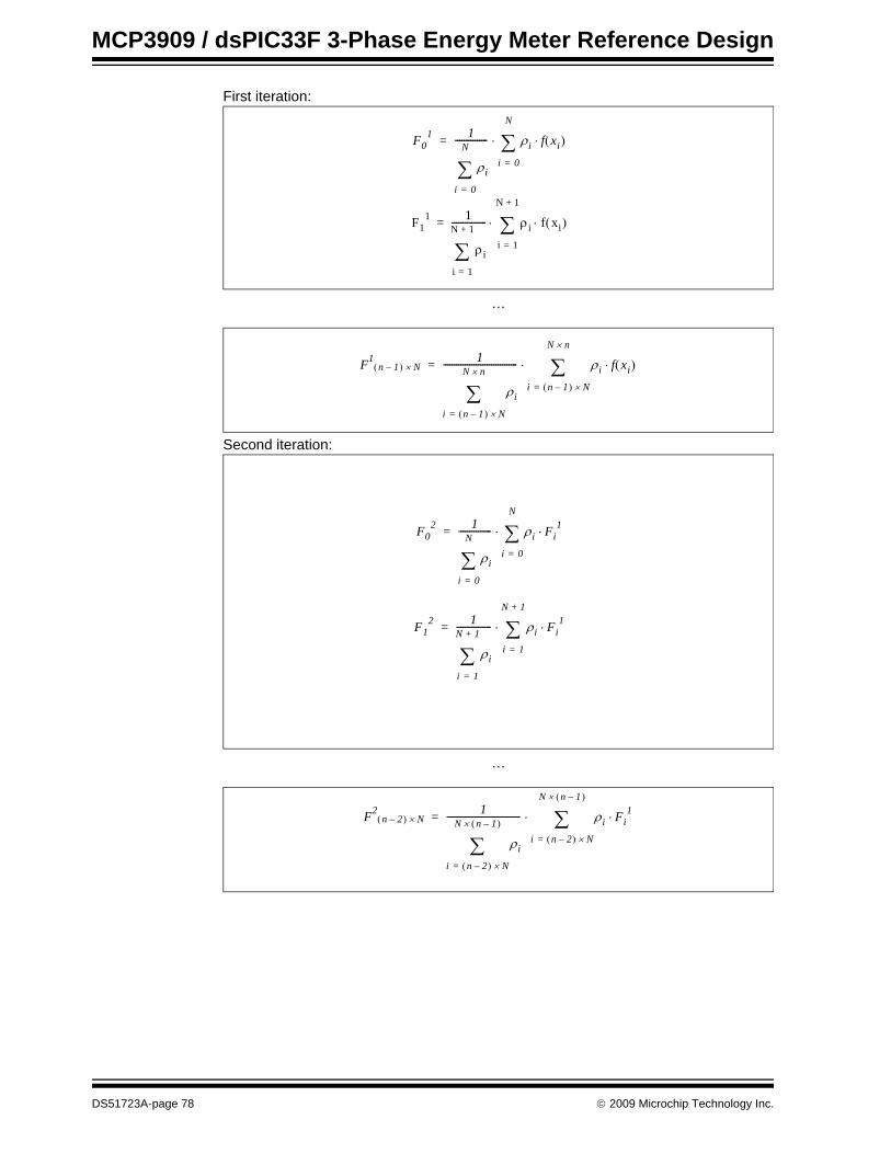
MCP3909 / dsPIC33F 3-Phase Energy Meter Reference Design
First iteration:
…
Second iteration:
…
F01 1
ρi
i 0=
N
∑
--------------- ρi
i 0=
N
∑ f xi( )⋅ ⋅=
F11 1
ρi
i 1=
N 1+
∑
---------------- ρi
i 1=
N 1+
∑ f xi( )⋅ ⋅=
F1n 1–( ) N×
1
ρi
i n 1–( ) N×=
N n×
∑
---------------------------------- ρi f xi( )⋅
i n 1–( ) N×=
N n×
∑⋅=
F02 1
ρi
i 0=
N
∑
--------------- ρi Fi1⋅
i 0=
N
∑⋅=
F12 1
ρi
i 1=
N 1+
∑
---------------- ρi
i 1=
N 1+
∑ Fi1⋅ ⋅=
F2n 2–( ) N×
1
ρi
i n 2–( ) N×=
N n 1–( )×
∑
---------------------------------- ρi
i n 2–( ) N×=
N n 1–( )×
∑ Fi1⋅ ⋅=
DS51723A-page 78 © 2009 Microchip Technology Inc.
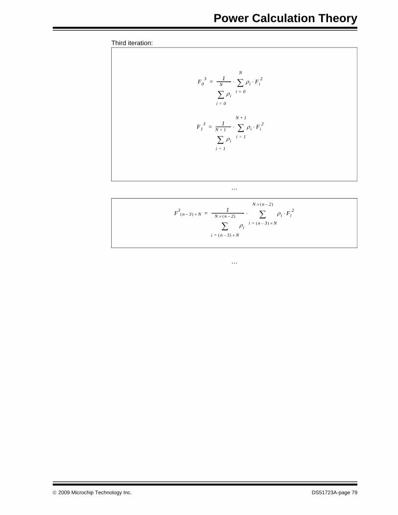
Power Calculation Theory
Third iteration:
…
…
F03 1
ρi
i 0=
N
∑
--------------- ρi
i 0=
N
∑ Fi2⋅ ⋅=
F13 1
ρi
i 1=
N 1+
∑
---------------- ρi
i 1=
N 1+
∑ Fi2⋅ ⋅=
F3n 3–( ) N×
1
ρi
i n 3–( ) N×=
N n 2–( )×
∑
---------------------------------- ρi
i n 3–( ) N×=
N n 2–( )×
∑ Fi2⋅ ⋅=
© 2009 Microchip Technology Inc. DS51723A-page 79
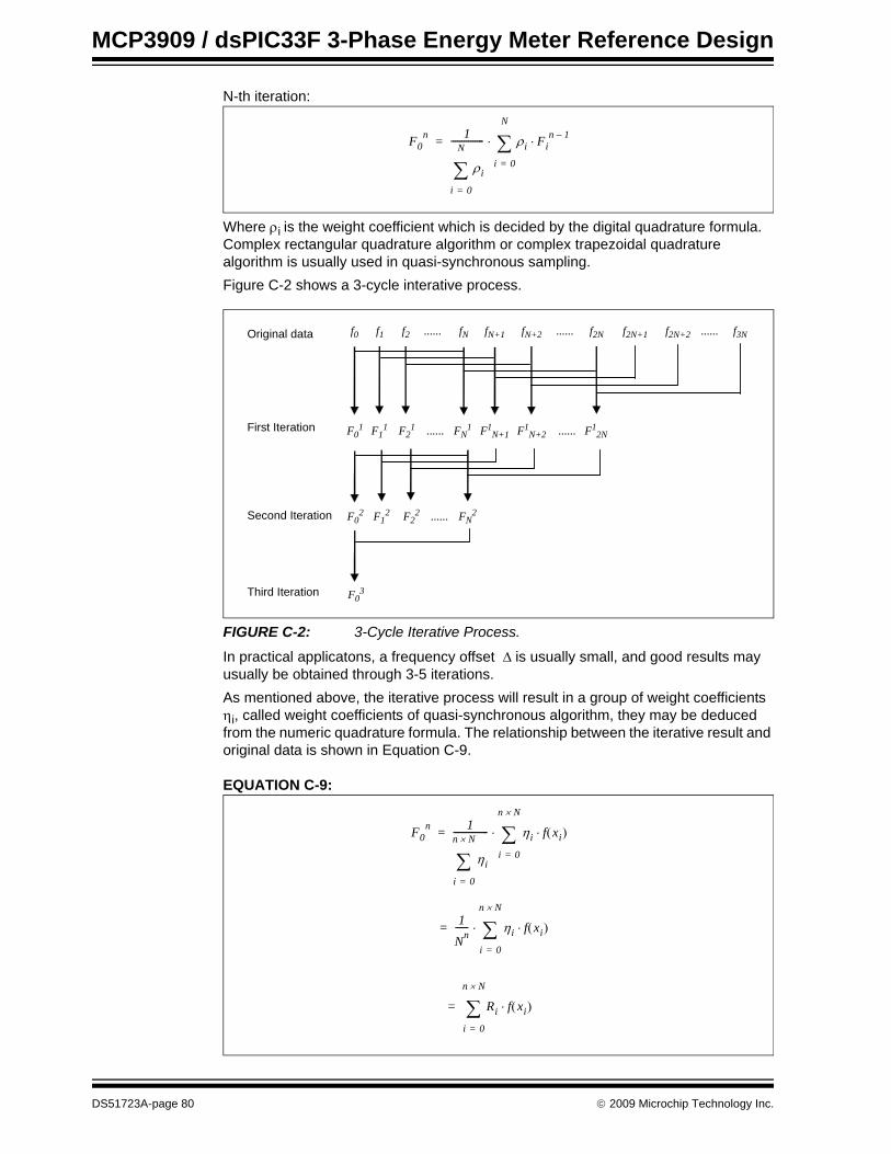
MCP3909 / dsPIC33F 3-Phase Energy Meter Reference Design
N-th iteration:
Where ρi is the weight coefficient which is decided by the digital quadrature formula. Complex rectangular quadrature algorithm or complex trapezoidal quadrature algorithm is usually used in quasi-synchronous sampling.Figure C-2 shows a 3-cycle interative process.
FIGURE C-2: 3-Cycle Iterative Process.
In practical applicatons, a frequency offset Δ is usually small, and good results may usually be obtained through 3-5 iterations.As mentioned above, the iterative process will result in a group of weight coefficients ηi, called weight coefficients of quasi-synchronous algorithm, they may be deduced from the numeric quadrature formula. The relationship between the iterative result and original data is shown in Equation C-9.
EQUATION C-9:
F0n 1
ρi
i 0=
N
∑
--------------- ρi
i 0=
N
∑ Fin 1–⋅ ⋅=
f0
F01
F02
F03
Original data
First Iteration
Second Iteration
Third Iteration
F12 F2
2 ...... FN2
F11 F2
1 ...... FN1 F1
N+1 F1N+2 ...... F1
2N
f1 f2 ...... fN fN+1 fN+2 ...... f2N f2N+1 f2N+2 ...... f3N
F0n 1
ηi
i 0=
n N×
∑
---------------- ηi f xi( )⋅
i 0=
n N×
∑⋅=
1Nn------ ηi f xi( )⋅
i 0=
n N×
∑⋅=
Ri f xi( )⋅
i 0=
n N×
∑=
DS51723A-page 80 © 2009 Microchip Technology Inc.

Power Calculation Theory
Where:
EQUATION C-10:
Equation C-10 is called the quasi-synchronous window function. After determining the sampling points, the number of iterations and numerical quadrature method, the coefficients of quasi-synchronous window function will become definite, and a quasi-synchronous window function arrays may be established in advance.Using the quasi-synchronous window function to carry out the weighted process of the original data is equivalent to carrying out data synchronization one time, and the algorithm realization is also very simple that only a multiplication of the original data and quasi-synchronous window function arrays is required. After processing, the new periodic signal will have the same period and frequency components as the original signal, and the synchronization error of the new signal becomes smaller.Figure C-3 is a schematic of the quasi-synchronous window function characteristics in the time domain and data processing. In Figure C-3, the red curve is the characteristic of the window function, and the blue curve is input signal, and the green curve is the output signal.
FIGURE C-3: Quasi-Synchronous Window Function Characteristics Curve and Data Processing.
Ri1
Nn------ ηi⋅= (i = 0 ~ n x N)
Am
plitu
de
Sampling point (1-193) Time 3.2 ksps
Window functionRaw dataData processed
© 2009 Microchip Technology Inc. DS51723A-page 81
MCP3909 / dsPIC33F 3-Phase Energy Meter Reference Design
C.3 THE HARMONIC ANALYSIS ALGORITHM OF QUASI-SYNCHRONOUS SAMPLING
Periodic signal can be expressed as trigonometric Fourier series or exponential Fourier series. A periodic signal with a period of T can be expressed as :
EQUATION C-11:
where:
EQUATION C-12:
EQUATION C-13:
or as:
EQUATION C-14:
where the relationship between ak, bk, ck and ϕk is:
EQUATION C-15:
EQUATION C-16:
EQUATION C-17:
f t( )α02
------- αk k ω t⋅ ⋅( )cos β k ω t⋅ ⋅( )cos+( )
k 1=
∞
∑+=
ak2T--- f t( )
0
T
∫ k ω t⋅ ⋅( )dtcos⋅ ⋅=
bk2T--- f t( )
0
T
∫ k ω t⋅ ⋅( )sin dt⋅ ⋅=
f t( ) a0 ck k ω t ϕk+⋅ ⋅( )sink 1=
∞
∑+=
ck ak2 bk
2+=
ϕkakbk-----atan=
ak ck ϕksin=
DS51723A-page 82 © 2009 Microchip Technology Inc.

Power Calculation Theory
EQUATION C-18:
Make g(t) = f(t) • cos(K•ω•t), it can be proved that g(t) is also a periondic function with T as its period. Averaging g(t) in the range of [0 ~ T] results in:
EQUATION C-19:
So ak = 2 × g(t). Therefore, ak can be obtained if only g(t) can be calculated.
EQUATION C-20:
EQUATION C-21:
Where N, n and ηi are constants. The equation may therefore be written as:
EQUATION C-22:
EQUATION C-23:
Where:
EQUATION C-24:
bk ck ϕkcos=
g t( ) 1T--- f t( )
0
T
∫ k ω t⋅ ⋅( )dtcos⋅ ⋅=
ak 2g t( ) 2Nn------ ηi gi⋅
i 0=
n N×
∑⋅= =
2Nn------ ηi fi k 2π
N------ i⋅ ⋅⎝ ⎠
⎛ ⎞cos⋅ ⋅
i 0=
n N×
∑⋅=
bk2
Nn------ ηi fi k 2π
N------ i⋅ ⋅⎝ ⎠
⎛ ⎞sin⋅ ⋅
i 0=
n N×
∑⋅=
ak Ii fi k 2πN------ i⋅ ⋅⎝ ⎠
⎛ ⎞cos⋅ ⋅
i 0=
n N×
∑=
bk Ii fi k 2πN------ i⋅ ⋅⎝ ⎠
⎛ ⎞sin⋅ ⋅
i 0=
n N×
∑=
Ii2
Nn------ η1 R1 2×=⋅= i 0 n N×∼=( )
© 2009 Microchip Technology Inc. DS51723A-page 83

MCP3909 / dsPIC33F 3-Phase Energy Meter Reference Design
C.4 MEASURING THE VOLTAGE/CURRENT RMS VALUE AND POWER USING QUASI-SYNCHRONOUS SAMPLING ALGORITHM
From Equation C-11, a periodic voltage can be expressed as:
EQUATION C-25:
So the voltage fundamental and the voltage of each harmonic can be expressed as:
EQUATION C-26:
From Equation C-25, the fundamental voltage and voltage of each harmonic can also be expressed as:
EQUATION C-27:
Where:
EQUATION C-28:
EQUATION C-29:
The voltage RMS value of each harmonic, then can be expressed as shown in Equation C-31 with its initial phase angle shown in Equation C-29.
EQUATION C-30:
U t( )Ua0
2----------- uak k ω t⋅ ⋅( )cos ubk k ω t⋅ ⋅( )sin+( )
k 1=
∞
∑+=
Uk t( ) uak k ω t⋅ ⋅( ) uk k ω t⋅ ⋅( )sin+cos=
Uk t( ) uck k ω t⋅ ⋅ ϕuk+( )sin=
uck uak2 ubk
2+=
ϕukuakubk-------atan=
Uk12
------- uckuak
2 ubk2+
2----------------------------=⋅=
DS51723A-page 84 © 2009 Microchip Technology Inc.

Power Calculation Theory
The relationship between uak, ubk and Uk can be expressed as:
EQUATION C-31:
EQUATION C-32:
Total effective voltage can be expressed as:
EQUATION C-33:
Similarly, the effective values and initial phase angles of fundamental current and current of each other harmonic can be expressed as:
EQUATION C-34:
EQUATION C-35:
The relationship between iak, ibk and Ik can be expressed as:
EQUATION C-36:
EQUATION C-37:
Total current RMS can be expressed as:
EQUATION C-38:
uak 2 Uk ϕuksin⋅ ⋅=
ubk 2 Uk ϕukcos⋅ ⋅=
Utotal Uk2
k 0=
∞
∑=
Ik12
------- ick⋅iak
2 ibk2+
2-------------------------= =
ϕikiakibk------atan=
iak 2 Ik ϕiksin⋅ ⋅=
ibk 2 Ik ϕikcos⋅ ⋅=
Itotal Ik2
k 0=
∞
∑=
© 2009 Microchip Technology Inc. DS51723A-page 85
MCP3909 / dsPIC33F 3-Phase Energy Meter Reference Design
According to the definition of power measurement, the active power and reactive power of the fundamental and each other harmonic can be expressed as:
EQUATION C-39:
EQUATION C-40:
Substituting Equation C-31, C-32, C-33 and C-37 into Equation C-39 and C-40, the power of each harmonic component can be obtained with the following:
EQUATION C-41:
EQUATION C-42:
Total active power and reactive power can be expressed as:
EQUATION C-43:
EQUATION C-44:
Pk UkIk ϕuk ϕik–( )cos=
12--- UkIk⋅ ϕuksin ϕiksin ϕukcos ϕikcos+( )=
Qk UkIk ϕuk ϕik–( )sin=
12--- UkIk⋅ ϕuksin ϕikcos ϕukcos ϕiksin–( )=
Pk12--- uakiak ubkiik+( )⋅=
Qk12--- uakiak ubkiik–( )⋅=
Ptotal Pk
k 0=
∞
∑=
Qtotal Qk
k 0=
∞
∑=
DS51723A-page 86 © 2009 Microchip Technology Inc.
Power Calculation Theory
C.5 MEASURING FREQUENCYThere are many ways to measure frequency, with the most common being counting the signal cycle. In this method, a counter increments each time a zero-crossing is detected. Based on the counts, the width of a cycle can be measured. If the zero-cross-ing is accurate and the counter precision is high enough, cycle counting can be a simple and practical method. But if the input signal has large harmonic components, causing distortion around zero-crossing, then this approach may produce large errors.Another method is to analyze and process the sampled data and calculate the frequen-cies. Analysis may be carried out in time domain, such as digital differential ND and interpolation method; or may be carried out in frequency domain after DFT transforma-tion, such as gravity center method, spectrum zoom method and phase difference method, among which the phase difference method is the most common one. It is not sensitive to signal distortion around zero-crossing points. The basic idea of the phase difference method is: if the rough range of to-be-measured signal frequency is known, then we may assume a frequency that is close to the actual frequency and then acquire an array of samples based on the assumed frequency. In the sampled data, the phase of the 1st cycle and the subsequent N-th cycle are meau-red and their difference may be calculated. Then the phase difference may be used to calculate the difference between the actual freqency and the assumed frequence, thus figuring out the actual frequency. If the frequency f0 to be measured is known to be a definite value f, i.e., f0 = f + Δf, Δf << f, then from Equation C-27, the fundamental signal can be expressed as:
EQUATION C-45:
If:
EQUATION C-46:
EQUATION C-47:
EQUATION C-48:
U1 t( ) uc1 ω t ϕu1+⋅( )sin uc1 2πf0t ϕu1+( )sin= =
T 1f---=
ua2T--- U1 t( ) ωt( )cos td
0
T
∫⋅=
2T--- uc1 2πf0t ϕu1+( ) 2πft( )cossin td
0
T
∫⋅=
ub2T--- U1 t( ) ωt( )sin td
0
T
∫⋅=
2T--- uc1 2πf0t ϕu1+( ) 2πft( )sinsin td
0
T
∫⋅=
© 2009 Microchip Technology Inc. DS51723A-page 87
MCP3909 / dsPIC33F 3-Phase Energy Meter Reference Design
We get:
EQUATION C-49:
EQUATION C-50:
As Δf << f, from Equation C-49 and C-50, we have:
EQUATION C-51:
Therefore,
EQUATION C-52:
Assuming that the signal's initial phase angle measured in the 1st cycle is ϕ1 and in the N-th is ϕN, then the difference between actual frequency and the assumed frequency is:
EQUATION C-53:
ua2uc1
T-----------
f Δf+( ) ϕu1( )sin πΔff
---------⎝ ⎠⎛ ⎞sin⋅ ⋅
π 2f Δf+( ) Δf⋅ ⋅-------------------------------------------------------------------------⋅=
ub2uc1
T-----------
f ϕu1( )cos πΔff
---------⎝ ⎠⎛ ⎞sin⋅ ⋅
π 2f Δf+( ) Δf⋅ ⋅--------------------------------------------------------⋅=
uaub-----
ϕu1( )sinϕu1( )cos
----------------------≈
⎪⎪⎪⎪⎪⎪
⎩
⎪⎪⎪⎪⎪⎪
⎨
⎧
><+
<>+
>>
<=
>=
≈
−
−
−
)0,0(,2)(
)0,0(,)(
)0,0(),(
)0,0(,2
3
)0,0(,2
1
1
11
abb
a
abb
a
abb
a
ab
ab
u
uuuutg
uuuutg
uuuu
tg
uu
uu
π
π
π
π
ϕ
⎪⎪⎪
⎩
⎪⎪⎪
⎨
⎧
>−⋅
⋅−−
−<−⋅
⋅+−
<−⋅
⋅−
≈Δ
)(,2
)2(
)(,2
)2(
)(,2
)(
11
11
11
πϕϕπ
πϕϕ
πϕϕπ
πϕϕ
πϕϕπ
ϕϕ
NN
NN
NN
Nf
Nf
Nf
f
DS51723A-page 88 © 2009 Microchip Technology Inc.
Power Calculation Theory
C.6 IMPROVING MEASUREMENT PRECISION OF QUASI-SYNCHRONOUS SAMPLING ALGORITHM
When using the quasi-synchronous sampling method for harmonic analysis and calculation of power as well as voltage and current, strict restrictions apply for the algorithm and compensation, (i.e., the frequency offset must not exceed 1% of the central frequency). Precision of the result increases as the frequency offset gets less. Measurement accuracy is not guaranteed, if this condition can not be met. Figure C-4 shows the quasi-synchronization algorithm using 3 iterations with input signal ranging from 47.5 Hz to 52.5 Hz. The algorithm is for calculating the active power, the reactive power and the relative error of current and voltage. Figure C-4 shows that the algorithm works well when the frequency falls in the range of 47.5 Hz to 52.5 Hz. As the frequency deviates from the range, the error increases significantly. Therefore, the algorithm needs to be improved to fit into more applications with a more relaxed restriction.
FIGURE C-4: Quasi-sync Algorithm Error Analysis of 3 Iterations.
The quasi-sync sampling algorithm has relative high accuracy in frequency measure-ment and the error can be less than 0.005 Hz. If the frequency range to be measured can be segmented to make the frequency input closest to the multiple of cycle point, and processed using appropriate quasi-sync window function and sine/cosine tale, then the algorithm can be used for a much wider range of frequency .Figure C-5 is the error analysis of the improved 3-iteration quasi-synchronous algorithm at 3.2 ksps. It shows that the relative error for each result can be well controlled when the frequency of the input signal falls in the range of 47.5 Hz to 52.5 Hz.Figure C-5 clearly shows that the relative errors of the current, voltage, active power and reactive power in the entire frequency range are less than 0.08%. Also, when the input frequency is around the multiple of cycle frequencies (52.459 Hz, 51.613 Hz, 50.794 Hz, 50.0 Hz, 49.231 Hz, 48.485 Hz and 47.761 Hz), the calculateion error is
© 2009 Microchip Technology Inc. DS51723A-page 89
MCP3909 / dsPIC33F 3-Phase Energy Meter Reference Design
minimal (<0.01%). When the input frequency deviates from the multiple of cycle frequencies, the calculation error increases rapidly. As the calculation error is related to the frequency offset to the multiple of freqency point, the calculation error caused by frequency offset can be corrected. Figure C-6 is the error analysis after frequency off-set correction using simple parabolic interpolation. Calcultion errors for all parameters are shown to be less than 0.015% after the correction.
FIGURE C-5: Error Analysis Of Improved Quasi-sync Calculation Using 3 Iterations.
FIGURE C-6: Calculation Error Analysis After The Frequency Offset Compensation.
DS51723A-page 90 © 2009 Microchip Technology Inc.

Power Calculation Theory
C.7 MEASURING SECONDARY PARAMETERSThe methods of measuring parameters such as RMS values of voltage and current, active power, reactive power and frequency have been discussed in previous sections. These are primary parameters that need to be calculated from the original data. There are some other parameters called secondary parameter, such as power factor of each phase, total reactive power, total active power, total power factor, harmonic components and cumulative energy. They are obtained indirectly from primary param-eters.The measurement of secondary parameters is discussed in this section.
C.7.0.1 TOTAL ACTIVE POWER AND TOTAL REACTIVE POWER
For 3-phase 4-wire systems, 3-phase total active power and recative power are the sum of power of each phase, respectively, which can be expressed as:
EQUATION C-54:
EQUATION C-55:
C.8 APPARENT POWER OF EACH PHASE AND TOTAL APPARENT POWER Apparent power is defined as:
EQUATION C-56:
C.9 POWER FACTOR OF EACH PHASE AND TOTAL POWER FACTORPower factor is defined as the ratio of active power to apparent power. The definition can be represented as shown in Equation C-57:
EQUATION C-57:
P PA PB PC+ +=
Q QA QB QC+ +=
S Q2 p2+=
PF P
P2 Q2+------------------------=
© 2009 Microchip Technology Inc. DS51723A-page 91

MCP3909 / dsPIC33F 3-Phase Energy Meter Reference Design
C.10 Active Energy AND REACTIVE ENERGYActive energy is defined as the integral of active power over time, which is:
EQUATION C-58:
In this design, active energy is obtained from multiplying the voltage by the current sampled each time. The phase angle difference is compensated after each power measurement is completed. For reactive power, the cumulative reactive energy over a time period can be calculated by measuring the average power and calculating the time interval between 2 measure-ments.
EQUATION C-59:
C.11 POSITIVE/NEGATIVE ACTIVE ENERGY, POSITIVE/NEGATIVE REACTIVE ENERGY AND FOUR-QUADRANT REACTIVE ENERGY
In the measurement plane, the horizontal axis denotes voltage vector U (fixed on the horizontal axis). The instantaneous current vector is used to represent the power transfer, and has a phase angle φ against vector U. φ is positive in counter-clockwise direction. Power exchange can be defined in 4 scenarios:• Quadrant I (P>0, Q>0): active energy and reactive energy are sent out at the
same time;• Quadrant II (P<0, Q>0): active energy is sent in while reactive energy is sent out; • Quadrant III (P<0, Q<0): active energy is sent in while reactive energy is
absorbed;• Quadrant IV (P>0, Q<0): active energy is sent out while the reactive energy is
absorbed.1. Positive active energy and negative active energy: accumulated active
energy can be defined as positive and negative depending on the direction of active current. When the direction of active current is positive (from power grid to loads), active energy is positive (where active power P>0, corresponding to quadrants I and IV, which means that loads are drawing energy from grid). When current moves from loads to power grid, it is defined as negative active energy (where active power P < 0, corresponding to quadrants II and III, which means energy is provided to grid). Usually only positive active energy is taken into account in active energy, but in practice negative active energy may be taken into account as well, if necessary.
2. Positive reactive energy and negative reactive energy: If reactive power Q > 0 (corresponding to quadrants I and II), it means power grid is providing reactive energy to loads, so the energy is defined as positive reactive energy. When reactive power Q < 0 (corresponding to quadrants III and IV), it means that loads are providing reactive energy to power grid, so the energy is defined as negative reactive energy.
W P t( ) td0
T
∫ u k( ) i k( ) Δt⋅ ⋅
k 0=
N
∑= =
Vr Q0
T
∫ t( )dt=
DS51723A-page 92 © 2009 Microchip Technology Inc.

Power Calculation Theory
3. Four-quadrant reactive energy: metering reactive energy in positive/negative reactive energy cannot truly reflect the status of reactive energy, whereas 4-quandrant reactive energy measuring gives a true picture of energy exchange. Reactive energy in four quadrants represents four different reactive energy (see Figure C-7). And the reactive energy is accumulated depending on which quadrant it is located.
FIGURE C-7: Definition Of 4 Quadrants To Measure Electrical Energy.
图2.4 电能测量四象限定义
Active in (+A)
I (RL)II (RC)
Φ
III (-RL) IV (-RC)
Reactive in (+R)
Reactive out (-R)
Active out (-A)
A-有功电能;R—无功电能;RL—感性无功电能;RC—容性无功电能
电流向量
电压向量
图2.4 电能测量四象限定义
Active in (+A)
I (RL)II (RC)
Φ
III (-RL) IV (-RC)
Reactive in (+R)
Reactive out (-R)
Active out (-A)
A-有功电能;R—无功电能;RL—感性无功电能;RC—容性无功电能
电流向量
电压向量
Active in (+A)
I (RL)II (RC)
Φ
III (-RL) IV (-RC)
Reactive in (+R)
Reactive out (-R)
Active out (-A)
A-有功电能;R—无功电能;RL—感性无功电能;RC—容性无功电能
Active in (+A)
I (RL)II (RC)
Φ
III (-RL) IV (-RC)
Reactive in (+R)
Reactive out (-R)
Active out (-A)
A-有功电能;R—无功电能;RL—感性无功电能;RC—容性无功电能
电流向量
电压向量Voltage vector
Current vector
Where:
A = is active energy,
R = is reactive energy
RL = is inductive reactive energy
RC = s capacitive reactive energy
© 2009 Microchip Technology Inc. DS51723A-page 93

MCP3909 / dsPIC33F 3-Phase Energy Meter Reference Design
C.12 HARMONIC COMPONENTS OF CURRENT, VOLTAGE AND TOTAL HARMONIC DISTORTION
In Section C.3 “The Harmonic Analysis Algorithm Of Quasi-synchronous Sam-pling”, we discussed the measuring of current and voltage signals for each order of harmonics. 3 parameters are used to show to what extent a distorted wave deviates from a sine wave. They are: harmonic content, total distortion and harmonic ratio of the k-th harmonic. The term harmonic content means the root of square of effective values for all harmonics, which is defined as:
EQUATION C-60:
The total voltage distortion ratio of harmonics is the ratio of harmonic content to the fundamental in percentage, which is defined as:
EQUATION C-61:
The k-th harmonic ratio for voltage is the ratio of the k-th harmonic to the fundamental in percentage, defined as:
EQUATION C-62:
Similarly, harmonics of each order for the current and total distortion ratio can be sorted out.
UH Uk2k 2=
N
∑=
THDUUHUI------- 100%× THDUk( )2
k 2=
N
∑=
THDUkUkU1------ 100%×=
DS51723A-page 94 © 2009 Microchip Technology Inc.
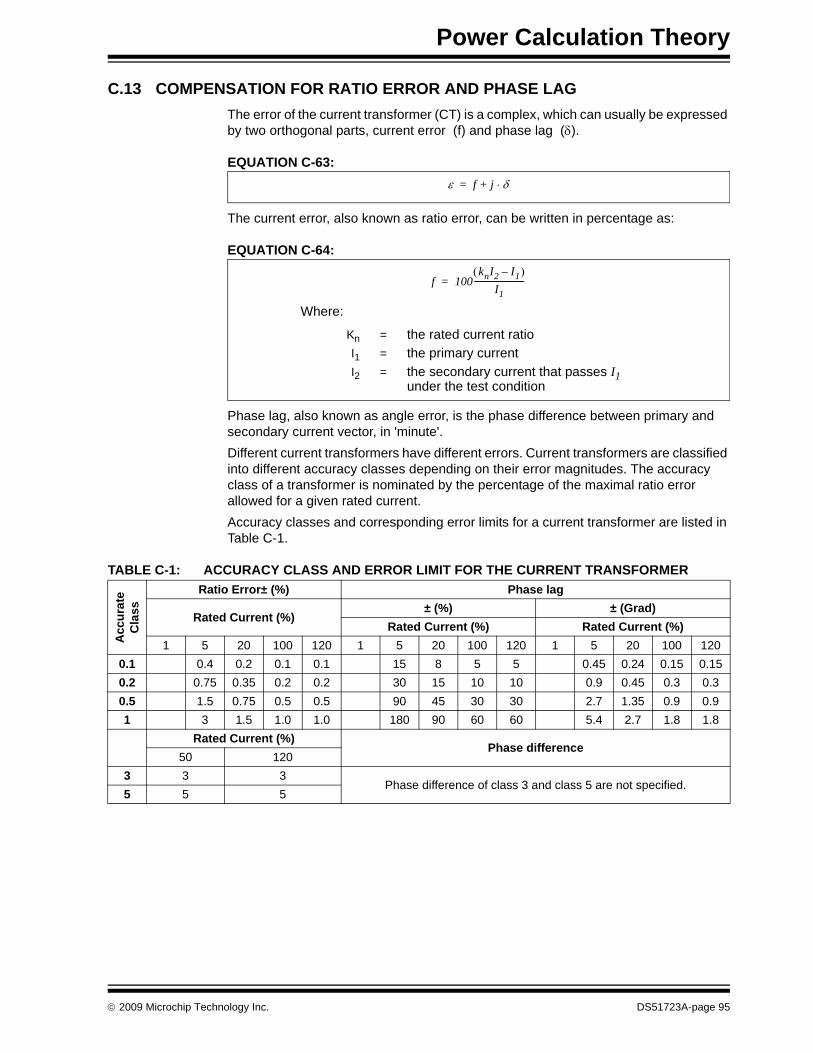
Power Calculation Theory
C.13 COMPENSATION FOR RATIO ERROR AND PHASE LAGThe error of the current transformer (CT) is a complex, which can usually be expressed by two orthogonal parts, current error (f) and phase lag (δ).
EQUATION C-63:
The current error, also known as ratio error, can be written in percentage as:
EQUATION C-64:
Phase lag, also known as angle error, is the phase difference between primary and secondary current vector, in 'minute'.Different current transformers have different errors. Current transformers are classified into different accuracy classes depending on their error magnitudes. The accuracy class of a transformer is nominated by the percentage of the maximal ratio error allowed for a given rated current.Accuracy classes and corresponding error limits for a current transformer are listed in Table C-1.
TABLE C-1: ACCURACY CLASS AND ERROR LIMIT FOR THE CURRENT TRANSFORMER
ε f j δ⋅+=
f 100knI2 I1–( )
I1-------------------------=
Where:
Kn = the rated current ratioI1 = the primary currentI2 = the secondary current that passes I1
under the test condition
Acc
urat
eC
lass
Ratio Error± (%) Phase lag
Rated Current (%)± (%) ± (Grad)
Rated Current (%) Rated Current (%)1 5 20 100 120 1 5 20 100 120 1 5 20 100 120
0.1 0.4 0.2 0.1 0.1 15 8 5 5 0.45 0.24 0.15 0.150.2 0.75 0.35 0.2 0.2 30 15 10 10 0.9 0.45 0.3 0.30.5 1.5 0.75 0.5 0.5 90 45 30 30 2.7 1.35 0.9 0.91 3 1.5 1.0 1.0 180 90 60 60 5.4 2.7 1.8 1.8
Rated Current (%)Phase difference
50 1203 3 3
Phase difference of class 3 and class 5 are not specified.5 5 5
© 2009 Microchip Technology Inc. DS51723A-page 95
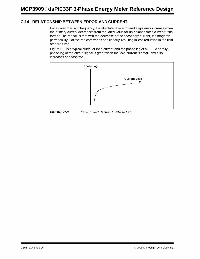
MCP3909 / dsPIC33F 3-Phase Energy Meter Reference Design
C.14 RELATIONSHIP BETWEEN ERROR AND CURRENTFor a given load and frequency, the absolute ratio error and angle error increase when the primary current decreases from the rated value for un-compensated current trans-former. The reason is that with the decrease of the secondary current, the magnetic permeability µ of the iron core varies non-linearly, resulting in less reduction in the field ampere turns.Figure C-8 is a typical curve for load current and the phase lag of a CT. Generally, phase lag of the output signal is great when the load current is small, and also increases at a fast rate.
FIGURE C-8: Current Load Versus CT Phase Lag.
Current Load
Phase Lag
DS51723A-page 96 © 2009 Microchip Technology Inc.
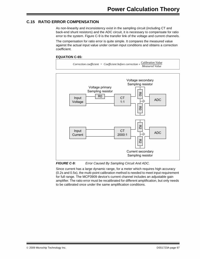
Power Calculation Theory
C.15 RATIO ERROR COMPENSATIONAs non-linearity and inconsistency exist in the sampling circuit (including CT and back-end shunt resistors) and the ADC circuit, it is necessary to compensate for ratio error to the system. Figure C-9 is the transfer link of the voltage and current channels.The compensation for ratio error is quite simple. It compares the measured value against the actual input value under certain input conditions and obtains a correction coefficient.
EQUATION C-65:
FIGURE C-9: Error Caused By Sampling Circuit And ADC.
Since current has a large dynamic range, for a meter which requires high accuracy (0.2s and 0.5s), the multi-point calibration method is needed to meet input requirement for full range. The MCP3909 device's current channel includes an adjustable gain amplifier. The ratio error must be recalibrated for different amplification, but only needs to be calibrated once under the same amplification conditions.
Correction coefficient Coefficient before correction Calibration ValueMeasured Value
-------------------------------------------×=
InputVoltage
R0 CT1:1 ADC
R0
R0
Voltage primarySampling resistor
Voltage secondarySampling resistor
InputCurrent
CT2000:1 ADC
R2
R2
Current secondarySampling resistor
© 2009 Microchip Technology Inc. DS51723A-page 97
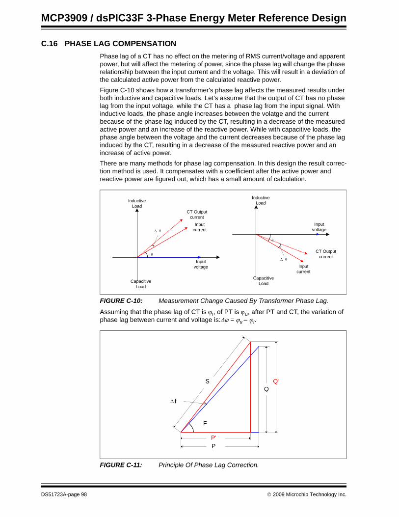
MCP3909 / dsPIC33F 3-Phase Energy Meter Reference Design
C.16 PHASE LAG COMPENSATIONPhase lag of a CT has no effect on the metering of RMS current/voltage and apparent power, but will affect the metering of power, since the phase lag will change the phase relationship between the input current and the voltage. This will result in a deviation of the calculated active power from the calculated reactive power.Figure C-10 shows how a transformer's phase lag affects the measured results under both inductive and capacitive loads. Let's assume that the output of CT has no phase lag from the input voltage, while the CT has a phase lag from the input signal. With inductive loads, the phase angle increases between the volatge and the current because of the phase lag induced by the CT, resulting in a decrease of the measured active power and an increase of the reactive power. While with capacitive loads, the phase angle between the voltage and the current decreases because of the phase lag induced by the CT, resulting in a decrease of the measured reactive power and an increase of active power.There are many methods for phase lag compensation. In this design the result correc-tion method is used. It compensates with a coefficient after the active power and reactive power are figured out, which has a small amount of calculation.
FIGURE C-10: Measurement Change Caused By Transformer Phase Lag.
Assuming that the phase lag of CT is ϕi, of PT is ϕu, after PT and CT, the variation of phase lag between current and voltage is:Δϕ = ϕu – ϕi.
FIGURE C-11: Principle Of Phase Lag Correction.
Input current
CT Output current
Input voltage
Capacitive Load
Inductive Load
Δθ
θ
Input current
CT Output current
Input voltage
Capacitive Load
Inductive Load
Δθ
θ
F
Δf
S
P'P
QQ'
DS51723A-page 98 © 2009 Microchip Technology Inc.

Power Calculation Theory
Given that the phase lag between the input voltage and current is φ, after PT and CT, the actual measured active power is P', reactive power is Q'. RMS current is I, RMS voltage is V, input apparent power is S, actual input active power is P and reactive power is Q, then Figure C-11 can be drawn based on the principles of power triangle.
EQUATION C-66:
EQUATION C-67:
From the above 2 equations, we have:
EQUATION C-68:
EQUATION C-69:
Where:
EQUATION C-70:
EQUATION C-71:
By setting up certain input conditions, Δϕ can be measured, and then k1 and k2 can be calculated.In this design, we use an input of 0.5L for calibration. With this condition, Δϕ can be calculated using the difference between the meaured and the actual input value of active power. For accurate calculations, the user may also use the difference between the measured cumulative energy and the actual cumulative energy to calculate the difference.
EQUATION C-72:
Where err is the error rate of the energy measurement, which results from calculating the error between the actual energy measured by a standard meter and the energy measured by the dsPIC devices. The error can be obtained from the output of the meter calibration workbench.
EQUATION C-73:
P' V I φ Δϕ+( )cos⋅ ⋅ P Δϕcos Q Δϕsin–= =
Q' V I φ Δϕ+( )sin⋅ ⋅ Q Δϕcos P Δϕsin–= =
P k1P' k2Q'+=
Q k1Q' k2P'–=
k1 Δϕcos=
k1 Δsin ϕ=
Δϕ a P'2 P⋅-----------⎝ ⎠
⎛ ⎞ π3---–cos a 0.5 1 err+( )⋅( ) π
3---–⎝ ⎠
⎛ ⎞cos= =
err P' P–P
-------------- ΔPP
------- 100×= =
© 2009 Microchip Technology Inc. DS51723A-page 99

MCP3909 / dsPIC33F 3-Phase Energy Meter Reference Design
Since the phase lag of a CT's output signal is related to the magnitude of current, different correction coefficients, K, can be set according to different RMS current values. In this design, 5 calibration points can be set. If it does not require high-preci-sion, fewer points can be set to simplify calibration.If one-time calibration cannot meet the precision requirement, more calibrations can be done. The new angle error may still be calculated using Equation C-72. The new correction coefficient is:
EQUATION C-74:
EQUATION C-75:
C.16.0.1 PHASE LAG COMPENSATION WHEN FREQUENCY VARIES
For the same current intensity, the signal delay caused by the CT is the same. When the frequency of the input signal varies, the phase lag will be different. Normally, calibration is done at 50 Hz. When the frequency varies, if the same phase lag compensation coefficient for 50 Hz is still used, it will cause an error in the power measurement. In most cases, the frequency varies in a small range (test specification requires ±2.5%), so it has little effect on the measurement accuracy. For meters with an accuracy of 0.5s or above, this measurement error can be ignored. But for 0.2s meters, the error cannot be ignored and the frequency variation needs to be corrected during calculation.The phase lag compensation coefficient k1 and k2 are corrected during calculation. Assuming that the freqnency is 50 Hz, the signal delay caused by CT is t, then after correction, the compensation coefficient k1 and k2 will be:
EQUATION C-76:
EQUATION C-77:
When frequency varies, assuming that the frequency offset is Δf, i.e. the input signal frequency is 50 + Δf, then the compensation coefficient will be:
EQUATION C-78:
EQUATION C-79:
k'1 Δϕ1 Δϕ2+( )cos k1 Δϕ2cos k2 Δϕ2sin⋅–⋅= =
k'2 Δϕ1 Δϕ2+( )sin k2 Δϕ2cos k1 Δϕ2sin⋅–⋅= =
k1 Δϕcos t 50 2π⋅ ⋅( )cos= =
k2 Δsin ϕ t 50 2π⋅ ⋅( )sin= =
k'1 Δϕcos t 50 Δf+( ) 2π⋅ ⋅( )cos= =
k'2 Δsin ϕ t 50 Δf+( ) 2π⋅ ⋅( )sin= =
DS51723A-page 100 © 2009 Microchip Technology Inc.

Power Calculation Theory
To avoid complexity in calculation and to maximize the correction precision, the following equations may be used to approximate K1 and K2 when the phase angle is small.
EQUATION C-80:
EQUATION C-81:
k'1 Δϕcos Δϕcos Δf50------ sin2Δϕ⋅–≈=
k1Δf50------ k2 k2⋅ ⋅–=
k'2 Δsin ϕ Δsin ϕ Δf50------ sinΔϕ Δϕcos⋅ ⋅–≈=
k2Δf50------ k1 k2⋅ ⋅–=
© 2009 Microchip Technology Inc. DS51723A-page 101

MCP3909 / dsPIC33F 3-Phase Energy Meter Reference Design
NOTES:
DS51723A-page 102 © 2009 Microchip Technology Inc.

MCP3909 / DSPIC33F 3-PHASEENERGY METER REFERENCE DESIGN
Appendix D. 50/60 Hz Meter Operation
D.1 FIRMWARE VERSIONSThere are two versions of firmware for the meter due to the quasi-synchronous sampling scheme employed by the dsPIC33F firmware. The design covers the frequency of rated frequency ±2.5 Hz.To change the rated frequency, just change the definition in the beginning of cacul.h - #define STD_FREQ 50.0.This is provided for download from Microchip’s website, file names and checksums below.At the same time you need to change the crystal to provide clock for metering IC.
TABLE D-1: FIRMWARE FILES
Line Frequency Firmware Name Hex File Checksum YXX VALUE50 Hz PM_1_50.ZIP TBD 3.857 MHz60 Hz PM_1_60.ZIP TBD TBD
© 2009 Microchip Technology Inc. DS51723A-page 103

DS51723A-page 104 © 2009 Microchip Technology Inc.
AMERICASCorporate Office2355 West Chandler Blvd.Chandler, AZ 85224-6199Tel: 480-792-7200 Fax: 480-792-7277Technical Support: http://support.microchip.comWeb Address: www.microchip.comAtlantaDuluth, GA Tel: 678-957-9614 Fax: 678-957-1455BostonWestborough, MA Tel: 774-760-0087 Fax: 774-760-0088ChicagoItasca, IL Tel: 630-285-0071 Fax: 630-285-0075ClevelandIndependence, OH Tel: 216-447-0464 Fax: 216-447-0643DallasAddison, TX Tel: 972-818-7423 Fax: 972-818-2924DetroitFarmington Hills, MI Tel: 248-538-2250Fax: 248-538-2260KokomoKokomo, IN Tel: 765-864-8360Fax: 765-864-8387Los AngelesMission Viejo, CA Tel: 949-462-9523 Fax: 949-462-9608Santa ClaraSanta Clara, CA Tel: 408-961-6444Fax: 408-961-6445TorontoMississauga, Ontario, CanadaTel: 905-673-0699 Fax: 905-673-6509
ASIA/PACIFICAsia Pacific OfficeSuites 3707-14, 37th FloorTower 6, The GatewayHarbour City, KowloonHong KongTel: 852-2401-1200Fax: 852-2401-3431Australia - SydneyTel: 61-2-9868-6733Fax: 61-2-9868-6755China - BeijingTel: 86-10-8528-2100 Fax: 86-10-8528-2104China - ChengduTel: 86-28-8665-5511Fax: 86-28-8665-7889China - Hong Kong SARTel: 852-2401-1200 Fax: 852-2401-3431China - NanjingTel: 86-25-8473-2460Fax: 86-25-8473-2470China - QingdaoTel: 86-532-8502-7355Fax: 86-532-8502-7205China - ShanghaiTel: 86-21-5407-5533 Fax: 86-21-5407-5066China - ShenyangTel: 86-24-2334-2829Fax: 86-24-2334-2393China - ShenzhenTel: 86-755-8203-2660 Fax: 86-755-8203-1760China - WuhanTel: 86-27-5980-5300Fax: 86-27-5980-5118China - XiamenTel: 86-592-2388138 Fax: 86-592-2388130China - XianTel: 86-29-8833-7252Fax: 86-29-8833-7256China - ZhuhaiTel: 86-756-3210040 Fax: 86-756-3210049
ASIA/PACIFICIndia - BangaloreTel: 91-80-3090-4444 Fax: 91-80-3090-4080India - New DelhiTel: 91-11-4160-8631Fax: 91-11-4160-8632India - PuneTel: 91-20-2566-1512Fax: 91-20-2566-1513Japan - YokohamaTel: 81-45-471- 6166 Fax: 81-45-471-6122Korea - DaeguTel: 82-53-744-4301Fax: 82-53-744-4302Korea - SeoulTel: 82-2-554-7200Fax: 82-2-558-5932 or 82-2-558-5934Malaysia - Kuala LumpurTel: 60-3-6201-9857Fax: 60-3-6201-9859Malaysia - PenangTel: 60-4-227-8870Fax: 60-4-227-4068Philippines - ManilaTel: 63-2-634-9065Fax: 63-2-634-9069SingaporeTel: 65-6334-8870Fax: 65-6334-8850Taiwan - Hsin ChuTel: 886-3-6578-300Fax: 886-3-6578-370Taiwan - KaohsiungTel: 886-7-536-4818Fax: 886-7-536-4803Taiwan - TaipeiTel: 886-2-2500-6610 Fax: 886-2-2508-0102Thailand - BangkokTel: 66-2-694-1351Fax: 66-2-694-1350
EUROPEAustria - WelsTel: 43-7242-2244-39Fax: 43-7242-2244-393Denmark - CopenhagenTel: 45-4450-2828 Fax: 45-4485-2829France - ParisTel: 33-1-69-53-63-20 Fax: 33-1-69-30-90-79Germany - MunichTel: 49-89-627-144-0 Fax: 49-89-627-144-44Italy - Milan Tel: 39-0331-742611 Fax: 39-0331-466781Netherlands - DrunenTel: 31-416-690399 Fax: 31-416-690340Spain - MadridTel: 34-91-708-08-90Fax: 34-91-708-08-91UK - WokinghamTel: 44-118-921-5869Fax: 44-118-921-5820
WORLDWIDE SALES AND SERVICE
03/26/09