doi: 10.1038/nmat3169 supplementary information...
TRANSCRIPT
1
Supplementary Information for
Synthesis of monolithic graphene – graphite integrated electronics
Jang-Ung Park1,2†�, SungWoo Nam3†�, Mi-Sun Lee1 & Charles M. Lieber2,3
1School of Nano-Biotechnology and Chemical Engineering, School of Mechanical and
Advanced Materials Engineering, Graphene Research Center, Ulsan National Institute of
Science and Technology (UNIST), Ulsan Metropolitan City, 689-798, Republic of Korea; 2Department of Chemistry and Chemical Biology, Harvard University, Cambridge,
Massachusetts 02138, USA; 3School of Engineering and Applied Sciences, Harvard
University, Cambridge, Massachusetts 02138, USA.
†J.-U. Park and S. Nam contributed equally.
�e-mail: [email protected]; [email protected].
SUPPLEMENTARY INFORMATIONDOI: 10.1038/NMAT3169
NATURE MATERIALS | www.nature.com/naturematerials 1
© 2011 Macmillan Publishers Limited. All rights reserved.
2
Supplementary Information
Methods
Preparation of metal catalysts.
(i) Synthesis of 2-4 layer graphene: a 700 nm-thick Cu layer was deposited using a
thermal evaporator on a Si wafer with 600 nm thermal oxide, and subsequently a 5 nm-
thick Ni layer was deposited on the Cu surface for passivation against Cu oxidation
caused by water and organic solvents during photolithography steps. We note that the use
of this top Ni layer is optional because the Cu oxide layer can be also reduced by flowing
H2 gas during CVD synthesis step. We observed that the existence of the ultra-thin top Ni
layer didn’t change the quality of the synthesized graphene.
(ii) ~850 layer graphite: a 400 nm-thick Co layer was thermally evaporated and patterned
on top of Cu / Ni film using bilayer photoresists (S1813, Shipley and LOR 3A,
MicroChem).
(iii) 6-8 layers: same procedure as (ii), except that a 20 nm-thick Ni (instead of the 400
nm-thick Co) layer was deposited.
When the Ni catalyst was used alone without Co and Cu, overall number of graphene
layers slightly increases with the thickness of Ni. However, we did not observe synthesis
of thick and uniform graphite structures (> 200 nm thick graphite), unlike when utilizing
the Co catalyst. Meanwhile, single or few-layer graphene (i.e. bilayer or thicker) was not
obtained by using only Co metal catalyst although the thickness was thin enough.
Synthesis of monolithic graphene-graphite. After loading the catalyst substrate onto
the edge of a quartz chemical vapor deposition (CVD) chamber, the furnace was heated
up to 1000 oC under the flow of H2 and Ar gases (H2: 1200 sccm, Ar: 500 sccm). As the
temperature reached at 1000 oC, the substrate was moved to the center of the heating zone
using a load-lock system for rapid thermal heating of substrate (movement duration: ~20
sec) to retard lateral diffusion of metals during temperature rising step. CVD growth was
carried out under atmospheric pressure with CH4 (25 sccm) and H2 (1200 sccm) for 4
minutes, and then the chamber was cooled to room temperature under the flow of Ar
(1200 sccm) over ca. 30 min. We note that the residue oxygen and water molecules
3
during the synthesis in atmospheric pressure can affect the level of defects (D bands in
Raman spectroscopy) and the device performances (mobility).
Transfer of the monolithic graphene-graphite. A 500 nm-thick poly(methyl
methacrylate) (MicroChem Corp., 950 PMMA) supporting layer was spun on the
synthesized graphene-graphite sample. The metal catalysts of Cu, Ni, and Co were
dissolved in a diluted etching solution of FeCl3: HCl: H2O (1:1:20 vol.%) with the
PMMA-coated graphene-graphite structure floating on the solution surface. Subsequently
the sample was transferred onto the surface of deionized water for rinsing. Finally, the
sample was transferred onto a target substrate, and the PMMA supporting layer was
removed with acetone. We note that the solution transfer method occasionally caused
cracks/tears (at the graphene-graphite interface) upon transfer, but advanced transfer
approaches1,2 can be utilized to improve the process. Furthermore, alternative transfer
approaches (e.g. dry3 or wedging4 transfer) can potentially allow the catalyst metal
substrate to be reused for additional growths as they do not require any wet-etching
process. In Fig. 3f, PMMA passivation pattern is located underneath the graphite
electrodes to prevent the direct electrical contact/shortage between the electrode and
water.
Measurement of sheet resistance. Films of graphene multilayers with different n-values
(n: ~2-4 layers, ~6-8 layers and ~850 layers) were synthesized, and then transferred onto
a Si wafer with 285 nm-thick thermal oxide. Sheet resistances of the films were measured
using a four-point probe setup (model: CMT-100MP, Advanced Instrument Technology,
Inc.).
Fabrication of monolithic graphene-graphite backgate field-effect transistors
(FETs). Monolithic graphene-graphite FET arrays were synthesized by using spatially
patterned catalyst metal films (Cu for graphene channel, and Co for graphite S/D) and
defined by using oxygen plasma etching before the transfer onto a substrate.
Subsequently, the patterned graphene-graphite FET structures were coated with the
PMMA supporting layer and then transferred onto a degenerately doped Si wafer with a
2 NATURE MATERIALS | www.nature.com/naturematerials
SUPPLEMENTARY INFORMATION DOI: 10.1038/NMAT3169
© 2011 Macmillan Publishers Limited. All rights reserved.
2
Supplementary Information
Methods
Preparation of metal catalysts.
(i) Synthesis of 2-4 layer graphene: a 700 nm-thick Cu layer was deposited using a
thermal evaporator on a Si wafer with 600 nm thermal oxide, and subsequently a 5 nm-
thick Ni layer was deposited on the Cu surface for passivation against Cu oxidation
caused by water and organic solvents during photolithography steps. We note that the use
of this top Ni layer is optional because the Cu oxide layer can be also reduced by flowing
H2 gas during CVD synthesis step. We observed that the existence of the ultra-thin top Ni
layer didn’t change the quality of the synthesized graphene.
(ii) ~850 layer graphite: a 400 nm-thick Co layer was thermally evaporated and patterned
on top of Cu / Ni film using bilayer photoresists (S1813, Shipley and LOR 3A,
MicroChem).
(iii) 6-8 layers: same procedure as (ii), except that a 20 nm-thick Ni (instead of the 400
nm-thick Co) layer was deposited.
When the Ni catalyst was used alone without Co and Cu, overall number of graphene
layers slightly increases with the thickness of Ni. However, we did not observe synthesis
of thick and uniform graphite structures (> 200 nm thick graphite), unlike when utilizing
the Co catalyst. Meanwhile, single or few-layer graphene (i.e. bilayer or thicker) was not
obtained by using only Co metal catalyst although the thickness was thin enough.
Synthesis of monolithic graphene-graphite. After loading the catalyst substrate onto
the edge of a quartz chemical vapor deposition (CVD) chamber, the furnace was heated
up to 1000 oC under the flow of H2 and Ar gases (H2: 1200 sccm, Ar: 500 sccm). As the
temperature reached at 1000 oC, the substrate was moved to the center of the heating zone
using a load-lock system for rapid thermal heating of substrate (movement duration: ~20
sec) to retard lateral diffusion of metals during temperature rising step. CVD growth was
carried out under atmospheric pressure with CH4 (25 sccm) and H2 (1200 sccm) for 4
minutes, and then the chamber was cooled to room temperature under the flow of Ar
(1200 sccm) over ca. 30 min. We note that the residue oxygen and water molecules
3
during the synthesis in atmospheric pressure can affect the level of defects (D bands in
Raman spectroscopy) and the device performances (mobility).
Transfer of the monolithic graphene-graphite. A 500 nm-thick poly(methyl
methacrylate) (MicroChem Corp., 950 PMMA) supporting layer was spun on the
synthesized graphene-graphite sample. The metal catalysts of Cu, Ni, and Co were
dissolved in a diluted etching solution of FeCl3: HCl: H2O (1:1:20 vol.%) with the
PMMA-coated graphene-graphite structure floating on the solution surface. Subsequently
the sample was transferred onto the surface of deionized water for rinsing. Finally, the
sample was transferred onto a target substrate, and the PMMA supporting layer was
removed with acetone. We note that the solution transfer method occasionally caused
cracks/tears (at the graphene-graphite interface) upon transfer, but advanced transfer
approaches1,2 can be utilized to improve the process. Furthermore, alternative transfer
approaches (e.g. dry3 or wedging4 transfer) can potentially allow the catalyst metal
substrate to be reused for additional growths as they do not require any wet-etching
process. In Fig. 3f, PMMA passivation pattern is located underneath the graphite
electrodes to prevent the direct electrical contact/shortage between the electrode and
water.
Measurement of sheet resistance. Films of graphene multilayers with different n-values
(n: ~2-4 layers, ~6-8 layers and ~850 layers) were synthesized, and then transferred onto
a Si wafer with 285 nm-thick thermal oxide. Sheet resistances of the films were measured
using a four-point probe setup (model: CMT-100MP, Advanced Instrument Technology,
Inc.).
Fabrication of monolithic graphene-graphite backgate field-effect transistors
(FETs). Monolithic graphene-graphite FET arrays were synthesized by using spatially
patterned catalyst metal films (Cu for graphene channel, and Co for graphite S/D) and
defined by using oxygen plasma etching before the transfer onto a substrate.
Subsequently, the patterned graphene-graphite FET structures were coated with the
PMMA supporting layer and then transferred onto a degenerately doped Si wafer with a
NATURE MATERIALS | www.nature.com/naturematerials 3
SUPPLEMENTARY INFORMATIONDOI: 10.1038/NMAT3169
© 2011 Macmillan Publishers Limited. All rights reserved.
4
285 nm-thick thermal oxide layer. PMMA layer was removed with acetone to yield
monolithic graphene-graphite backgate FETs. Thermal annealing treatment (~300 °C,
vacuum) of monolithic graphene-graphite FET devices was performed for ~3 hrs to
remove resist residues on graphene/graphite surface.
Assembly and fabrication of monolithic graphene-graphite topgate FETs. We have
employed two approaches to vertically integrate/assemble monolithic graphene-graphite
topgate FETs.
(i) As demonstrated in Fig. 4, we transferred the monolithic graphene-graphite structures
onto a flexible and transparent polyether ether ketone (PEEK) film where a 50 nm-thick
SiO2 adhesive layer was pre-deposited using an e-beam evaporator. After covering probe-
contact pads of graphite S/D electrodes with a PDMS shadow mask, a 400 nm-thick SiO2
layer was evaporated on the sample as a gate dielectric. Subsequently, the PDMS mask
was removed, and then a graphite film (6-8 graphene layers) for topgate was transferred
onto the area covered with the SiO2 dielectric layer. Finally, the topgate structures were
defined using the oxygen plasma etching.
(ii) We also demonstrated that the pre-patterned graphite topgate lines can be directly
assembled/bonded using a polymeric adhesive layer onto a dielectric layer covered
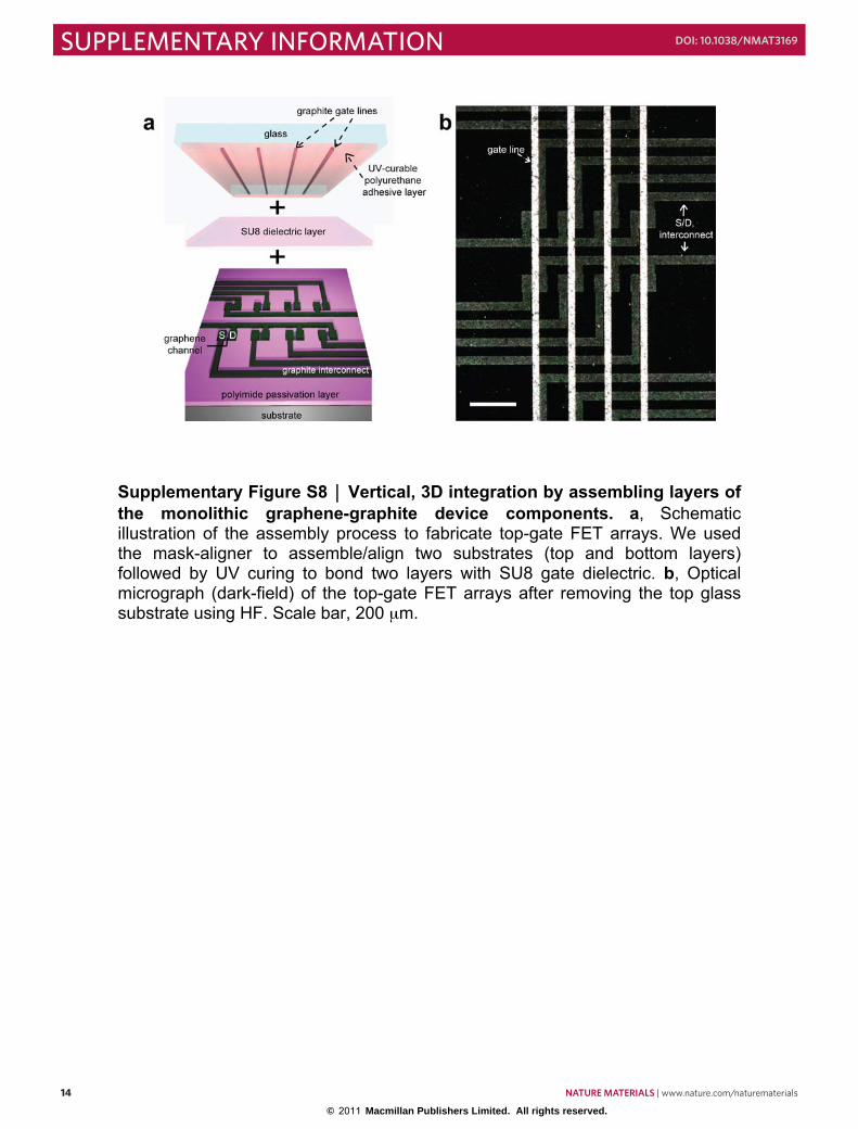
monolithic graphene channels and graphite S/D and interconnects, as illustrated in Fig.
S8. For this approach, the synthesized monolithic structures (graphene channel, and
graphite S/D and interconnects) were transferred onto a Si substrate pre-coated with a
polyimide passivation layer (thickness: ~2 µm). Also, the graphite topgate lines were
defined using oxygen plasma etching and then transferred onto a glass slide (thickness: ~
100 µm). A SU8 dielectric layer (thickness: 500 nm, Microchem) was coated onto the
substrate containing graphene channel with graphite S/D electrodes and interconnects,
and a UV-curable polyurethane adhesive layer (thickness: ~700 nm, Norland Optical
Adhesive 75) was spun on the glass slide with the topgate lines. The two substrates were
aligned using a mask-aligner (ABM, Inc.) and then bonded by UV exposure. Finally,
monolithic graphene-graphite topgate FET arrays were fabricated by removing the top
glass substrate in HF. We note that topgate FET fabricated by process (i) showed higher
transconductance levels due to thinner and higher-κ gate dielectrics.
5
Raman characterization. The Raman spectra were recorded with a WITec CRM200
Raman system with a 532 nm laser as excitation source using 100× objective lens (spot
size ~1 µm). We note that our Raman mapping result (Fig. 1d) had limited spatial
resolution (few µm).
Electrical characterization. (1) Back- and top-gate measurements were conducted with
a probe station (model 12561B, Cascade Microtech) with a computer-controlled analog-
to-digital converter (model 6030E, National Instruments) and a variable gain amplifier
(1211 current preamplifier, DL Instruments, Inc.). (2) Multichannel pH sensing was
carried out by monitoring the conductance with AC bias (79 Hz) and DC bias set to 0 V.
The drain current from multiple devices was amplified with custom-designed variable
gain amplifiers (multi-channel current preamplifier, SciMath Systems, LLC) and filtered
using a computer-based virtual lock-in amplifiers (multiplex 128-channel digital lock-in
amplifier set-up kit, National Instruments) with time constant set to 300 ms. Time-variant
conductance changes were recorded while different pH solutions were delivered through
a microfluidic channel. Watergate characterization was carried out using the same
measurement setup by sweeping Ag/AgCl reference electrode (inserted into the
microfluidic chamber) with a sweeping speed of 5 mV/sec. (3) We performed mechanical
deflection of suspended graphite electrodes by motor-driven micromanipulator to
precisely control the position and movement. Electrical measurements were obtained (Fig.
2f) with a variable gain amplifier (1211 current preamplifier, DL Instruments, Inc.).
Euler–Bernoulli beam theory5 was used to estimate the strain resulting from mechanical
deflection.
TEM characterization. The synthesized monolithic graphene-graphite structure was
transferred on a micromachined holey carbon grid (4220G-XA (R 1.2/1.3), SPI supplies).
High-resolution transmission electron microscopy (HRTEM) and diffraction pattern
analyses were carried out in a JEOL 2100F TEM (Cs corrector). The cross-sectional
image was observed at acceleration voltage of 200 kV by focusing the edge area of the
graphene-graphite interface.
4 NATURE MATERIALS | www.nature.com/naturematerials
SUPPLEMENTARY INFORMATION DOI: 10.1038/NMAT3169
© 2011 Macmillan Publishers Limited. All rights reserved.
4
285 nm-thick thermal oxide layer. PMMA layer was removed with acetone to yield
monolithic graphene-graphite backgate FETs. Thermal annealing treatment (~300 °C,
vacuum) of monolithic graphene-graphite FET devices was performed for ~3 hrs to
remove resist residues on graphene/graphite surface.
Assembly and fabrication of monolithic graphene-graphite topgate FETs. We have
employed two approaches to vertically integrate/assemble monolithic graphene-graphite
topgate FETs.
(i) As demonstrated in Fig. 4, we transferred the monolithic graphene-graphite structures
onto a flexible and transparent polyether ether ketone (PEEK) film where a 50 nm-thick
SiO2 adhesive layer was pre-deposited using an e-beam evaporator. After covering probe-
contact pads of graphite S/D electrodes with a PDMS shadow mask, a 400 nm-thick SiO2
layer was evaporated on the sample as a gate dielectric. Subsequently, the PDMS mask
was removed, and then a graphite film (6-8 graphene layers) for topgate was transferred
onto the area covered with the SiO2 dielectric layer. Finally, the topgate structures were
defined using the oxygen plasma etching.
(ii) We also demonstrated that the pre-patterned graphite topgate lines can be directly
assembled/bonded using a polymeric adhesive layer onto a dielectric layer covered
monolithic graphene channels and graphite S/D and interconnects, as illustrated in Fig.
S8. For this approach, the synthesized monolithic structures (graphene channel, and
graphite S/D and interconnects) were transferred onto a Si substrate pre-coated with a
polyimide passivation layer (thickness: ~2 µm). Also, the graphite topgate lines were
defined using oxygen plasma etching and then transferred onto a glass slide (thickness: ~
100 µm). A SU8 dielectric layer (thickness: 500 nm, Microchem) was coated onto the
substrate containing graphene channel with graphite S/D electrodes and interconnects,
and a UV-curable polyurethane adhesive layer (thickness: ~700 nm, Norland Optical
Adhesive 75) was spun on the glass slide with the topgate lines. The two substrates were
aligned using a mask-aligner (ABM, Inc.) and then bonded by UV exposure. Finally,
monolithic graphene-graphite topgate FET arrays were fabricated by removing the top
glass substrate in HF. We note that topgate FET fabricated by process (i) showed higher
transconductance levels due to thinner and higher-κ gate dielectrics.
5
Raman characterization. The Raman spectra were recorded with a WITec CRM200
Raman system with a 532 nm laser as excitation source using 100× objective lens (spot
size ~1 µm). We note that our Raman mapping result (Fig. 1d) had limited spatial
resolution (few µm).
Electrical characterization. (1) Back- and top-gate measurements were conducted with
a probe station (model 12561B, Cascade Microtech) with a computer-controlled analog-
to-digital converter (model 6030E, National Instruments) and a variable gain amplifier
(1211 current preamplifier, DL Instruments, Inc.). (2) Multichannel pH sensing was
carried out by monitoring the conductance with AC bias (79 Hz) and DC bias set to 0 V.
The drain current from multiple devices was amplified with custom-designed variable
gain amplifiers (multi-channel current preamplifier, SciMath Systems, LLC) and filtered
using a computer-based virtual lock-in amplifiers (multiplex 128-channel digital lock-in
amplifier set-up kit, National Instruments) with time constant set to 300 ms. Time-variant
conductance changes were recorded while different pH solutions were delivered through
a microfluidic channel. Watergate characterization was carried out using the same
measurement setup by sweeping Ag/AgCl reference electrode (inserted into the
microfluidic chamber) with a sweeping speed of 5 mV/sec. (3) We performed mechanical
deflection of suspended graphite electrodes by motor-driven micromanipulator to
precisely control the position and movement. Electrical measurements were obtained (Fig.
2f) with a variable gain amplifier (1211 current preamplifier, DL Instruments, Inc.).
Euler–Bernoulli beam theory5 was used to estimate the strain resulting from mechanical
deflection.
TEM characterization. The synthesized monolithic graphene-graphite structure was
transferred on a micromachined holey carbon grid (4220G-XA (R 1.2/1.3), SPI supplies).
High-resolution transmission electron microscopy (HRTEM) and diffraction pattern
analyses were carried out in a JEOL 2100F TEM (Cs corrector). The cross-sectional
image was observed at acceleration voltage of 200 kV by focusing the edge area of the
graphene-graphite interface.
NATURE MATERIALS | www.nature.com/naturematerials 5
SUPPLEMENTARY INFORMATIONDOI: 10.1038/NMAT3169
© 2011 Macmillan Publishers Limited. All rights reserved.
6
Watergate mobility calculation. Watergate mobility was estimated based on
considering series connection of double layer capacitance (CDL, including diffuse-layer
capacitance) and quantum capacitance (CQ). Devices were characterized in 100 µM
buffer solution (Debye length of ~30 nm), which gives CDL of ~2.3 µF/cm2 (CDL ~ ε0ε/d =
(8.85 × 10⁻¹² F/m × 80) / 30 nm). With an estimated quantum capacitance of ~3 µF/cm2
(ref 6), total capacitance of ~1.3 µF/cm2 is calculated, which resulted in water-gate field-
effect mobility of 850 cm2/V•s.
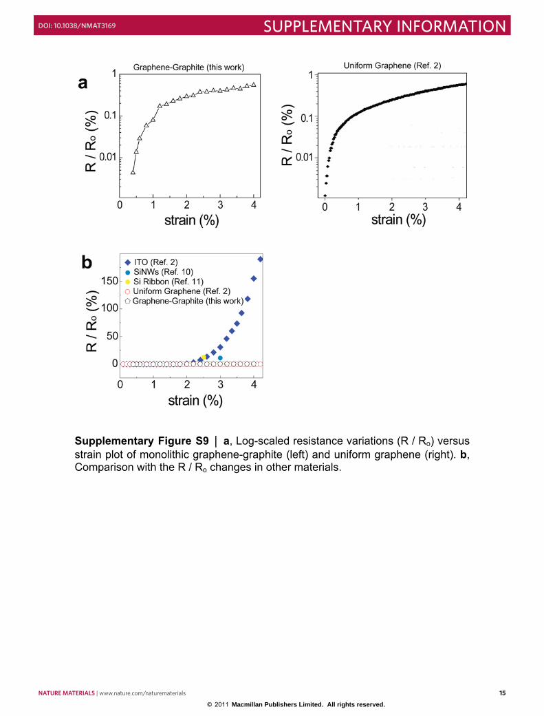
Strain analysis. The synthesized monolithic graphene-graphite film was transferred onto
a polyethylene terephthalate (PET) sheet (thickness: ~180 µm) for the resistance
measurement in Supplementary Fig. S9. Strain in the film is caused by externally applied
bending moment, and this strain can be calculated by the equation below2,7:
where R, ts, and tf are bending radius, thickness of substrate, and thickness of graphene-
graphite film, respectively (ts � tf). Also, η = tf / ts ≈ 0, and χ = [(Young’s modulus of
graphene-graphite film)/(Young’s modulus of substrate)].
7
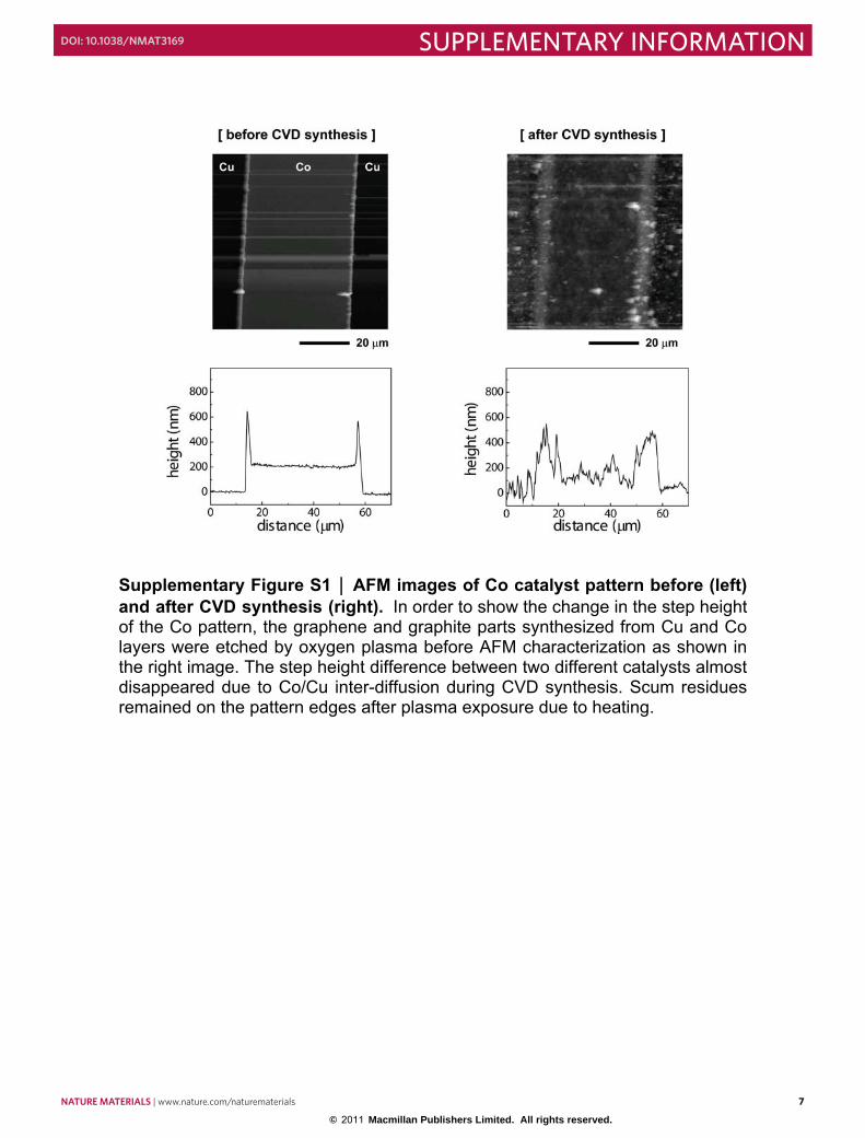
Supplementary Figure S1 ⎪ AFM images of Co catalyst pattern before (left) and after CVD synthesis (right). In order to show the change in the step height of the Co pattern, the graphene and graphite parts synthesized from Cu and Co layers were etched by oxygen plasma before AFM characterization as shown in the right image. The step height difference between two different catalysts almost disappeared due to Co/Cu inter-diffusion during CVD synthesis. Scum residues remained on the pattern edges after plasma exposure due to heating.
6 NATURE MATERIALS | www.nature.com/naturematerials
SUPPLEMENTARY INFORMATION DOI: 10.1038/NMAT3169
© 2011 Macmillan Publishers Limited. All rights reserved.
6
Watergate mobility calculation. Watergate mobility was estimated based on
considering series connection of double layer capacitance (CDL, including diffuse-layer
capacitance) and quantum capacitance (CQ). Devices were characterized in 100 µM
buffer solution (Debye length of ~30 nm), which gives CDL of ~2.3 µF/cm2 (CDL ~ ε0ε/d =
(8.85 × 10⁻¹² F/m × 80) / 30 nm). With an estimated quantum capacitance of ~3 µF/cm2
(ref 6), total capacitance of ~1.3 µF/cm2 is calculated, which resulted in water-gate field-
effect mobility of 850 cm2/V•s.
Strain analysis. The synthesized monolithic graphene-graphite film was transferred onto
a polyethylene terephthalate (PET) sheet (thickness: ~180 µm) for the resistance
measurement in Supplementary Fig. S9. Strain in the film is caused by externally applied
bending moment, and this strain can be calculated by the equation below2,7:
where R, ts, and tf are bending radius, thickness of substrate, and thickness of graphene-
graphite film, respectively (ts � tf). Also, η = tf / ts ≈ 0, and χ = [(Young’s modulus of
graphene-graphite film)/(Young’s modulus of substrate)].
7
Supplementary Figure S1 ⎪ AFM images of Co catalyst pattern before (left) and after CVD synthesis (right). In order to show the change in the step height of the Co pattern, the graphene and graphite parts synthesized from Cu and Co layers were etched by oxygen plasma before AFM characterization as shown in the right image. The step height difference between two different catalysts almost disappeared due to Co/Cu inter-diffusion during CVD synthesis. Scum residues remained on the pattern edges after plasma exposure due to heating.
NATURE MATERIALS | www.nature.com/naturematerials 7
SUPPLEMENTARY INFORMATIONDOI: 10.1038/NMAT3169
© 2011 Macmillan Publishers Limited. All rights reserved.
8
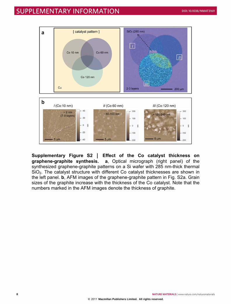
Supplementary Figure S2 ⎪ Effect of the Co catalyst thickness on graphene-graphite synthesis. a, Optical micrograph (right panel) of the synthesized graphene-graphite patterns on a Si wafer with 285 nm-thick thermal SiO2. The catalyst structure with different Co catalyst thicknesses are shown in the left panel. b, AFM images of the graphene-graphite pattern in Fig. S2a. Grain sizes of the graphite increase with the thickness of the Co catalyst. Note that the numbers marked in the AFM images denote the thickness of graphite.
9
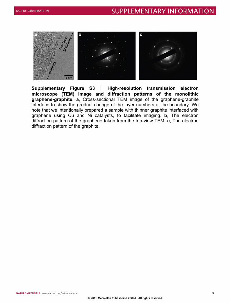
Supplementary Figure S3 ⎪ High-resolution transmission electron microscope (TEM) image and diffraction patterns of the monolithic graphene-graphite. a, Cross-sectional TEM image of the graphene-graphite interface to show the gradual change of the layer numbers at the boundary. We note that we intentionally prepared a sample with thinner graphite interfaced with graphene using Cu and Ni catalysts, to facilitate imaging. b, The electron diffraction pattern of the graphene taken from the top-view TEM. c, The electron diffraction pattern of the graphite.
8 NATURE MATERIALS | www.nature.com/naturematerials
SUPPLEMENTARY INFORMATION DOI: 10.1038/NMAT3169
© 2011 Macmillan Publishers Limited. All rights reserved.
8
Supplementary Figure S2 ⎪ Effect of the Co catalyst thickness on graphene-graphite synthesis. a, Optical micrograph (right panel) of the synthesized graphene-graphite patterns on a Si wafer with 285 nm-thick thermal SiO2. The catalyst structure with different Co catalyst thicknesses are shown in the left panel. b, AFM images of the graphene-graphite pattern in Fig. S2a. Grain sizes of the graphite increase with the thickness of the Co catalyst. Note that the numbers marked in the AFM images denote the thickness of graphite.
9
Supplementary Figure S3 ⎪ High-resolution transmission electron microscope (TEM) image and diffraction patterns of the monolithic graphene-graphite. a, Cross-sectional TEM image of the graphene-graphite interface to show the gradual change of the layer numbers at the boundary. We note that we intentionally prepared a sample with thinner graphite interfaced with graphene using Cu and Ni catalysts, to facilitate imaging. b, The electron diffraction pattern of the graphene taken from the top-view TEM. c, The electron diffraction pattern of the graphite.
NATURE MATERIALS | www.nature.com/naturematerials 9
SUPPLEMENTARY INFORMATIONDOI: 10.1038/NMAT3169
© 2011 Macmillan Publishers Limited. All rights reserved.
10
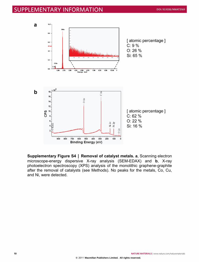
Supplementary Figure S4 ⎪ Removal of catalyst metals. a, Scanning electron microscope-energy dispersive X-ray analysis (SEM-EDAX) and b, X-ray photoelectron spectroscopy (XPS) analysis of the monolithic graphene-graphite after the removal of catalysts (see Methods). No peaks for the metals, Co, Cu, and Ni, were detected.
11
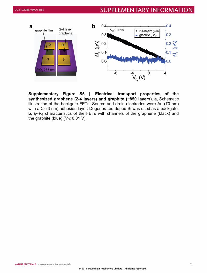
Supplementary Figure S5 ⎪ Electrical transport properties of the synthesized graphene (2-4 layers) and graphite (~850 layers). a, Schematic illustration of the backgate FETs. Source and drain electrodes were Au (70 nm) with a Cr (3 nm) adhesion layer. Degenerated doped Si was used as a backgate. b, ID-VG characteristics of the FETs with channels of the graphene (black) and the graphite (blue) (VD: 0.01 V).
10 NATURE MATERIALS | www.nature.com/naturematerials
SUPPLEMENTARY INFORMATION DOI: 10.1038/NMAT3169
© 2011 Macmillan Publishers Limited. All rights reserved.
10
Supplementary Figure S4 ⎪ Removal of catalyst metals. a, Scanning electron microscope-energy dispersive X-ray analysis (SEM-EDAX) and b, X-ray photoelectron spectroscopy (XPS) analysis of the monolithic graphene-graphite after the removal of catalysts (see Methods). No peaks for the metals, Co, Cu, and Ni, were detected.
11
Supplementary Figure S5 ⎪ Electrical transport properties of the synthesized graphene (2-4 layers) and graphite (~850 layers). a, Schematic illustration of the backgate FETs. Source and drain electrodes were Au (70 nm) with a Cr (3 nm) adhesion layer. Degenerated doped Si was used as a backgate. b, ID-VG characteristics of the FETs with channels of the graphene (black) and the graphite (blue) (VD: 0.01 V).
NATURE MATERIALS | www.nature.com/naturematerials 11
SUPPLEMENTARY INFORMATIONDOI: 10.1038/NMAT3169
© 2011 Macmillan Publishers Limited. All rights reserved.
12
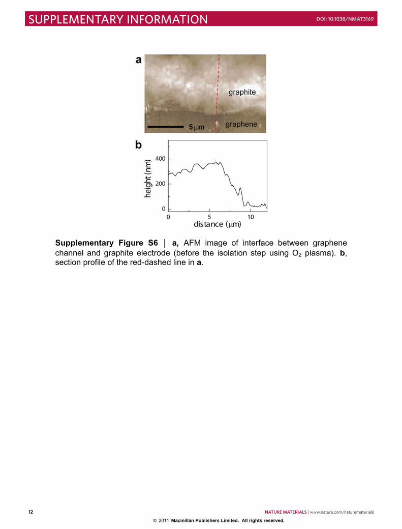
Supplementary Figure S6 ⎪ a, AFM image of interface between graphene channel and graphite electrode (before the isolation step using O2 plasma). b, section profile of the red-dashed line in a.
13
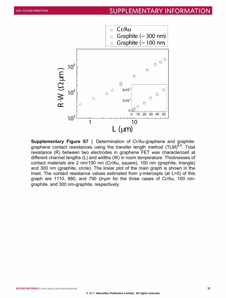
Supplementary Figure S7 ⎪ Determination of Cr/Au-graphene and graphite-graphene contact resistances using the transfer length method (TLM)8,9. Total resistance (R) between two electrodes in graphene FET was characterized at different channel lengths (L) and widths (W) in room temperature. Thicknesses of contact materials are 2 nm/100 nm (Cr/Au, square), 100 nm (graphite, triangle) and 300 nm (graphite, circle). The linear plot of the main graph is shown in the inset. The contact resistance values estimated from y-intercepts (at L=0) of this graph are 1110, 880, and 790 Ω•µm for the three cases of Cr/Au, 100 nm-graphite, and 300 nm-graphite, respectively.
12 NATURE MATERIALS | www.nature.com/naturematerials
SUPPLEMENTARY INFORMATION DOI: 10.1038/NMAT3169
© 2011 Macmillan Publishers Limited. All rights reserved.
12
Supplementary Figure S6 ⎪ a, AFM image of interface between graphene channel and graphite electrode (before the isolation step using O2 plasma). b, section profile of the red-dashed line in a.
13
Supplementary Figure S7 ⎪ Determination of Cr/Au-graphene and graphite-graphene contact resistances using the transfer length method (TLM)8,9. Total resistance (R) between two electrodes in graphene FET was characterized at different channel lengths (L) and widths (W) in room temperature. Thicknesses of contact materials are 2 nm/100 nm (Cr/Au, square), 100 nm (graphite, triangle) and 300 nm (graphite, circle). The linear plot of the main graph is shown in the inset. The contact resistance values estimated from y-intercepts (at L=0) of this graph are 1110, 880, and 790 Ω•µm for the three cases of Cr/Au, 100 nm-graphite, and 300 nm-graphite, respectively.
NATURE MATERIALS | www.nature.com/naturematerials 13
SUPPLEMENTARY INFORMATIONDOI: 10.1038/NMAT3169
© 2011 Macmillan Publishers Limited. All rights reserved.
14
Supplementary Figure S8 ⎪ Vertical, 3D integration by assembling layers of the monolithic graphene-graphite device components. a, Schematic illustration of the assembly process to fabricate top-gate FET arrays. We used the mask-aligner to assemble/align two substrates (top and bottom layers) followed by UV curing to bond two layers with SU8 gate dielectric. b, Optical micrograph (dark-field) of the top-gate FET arrays after removing the top glass substrate using HF. Scale bar, 200 µm.
15
Supplementary Figure S9 ⎪ a, Log-scaled resistance variations (R / Ro) versus strain plot of monolithic graphene-graphite (left) and uniform graphene (right). b, Comparison with the R / Ro changes in other materials.
14 NATURE MATERIALS | www.nature.com/naturematerials
SUPPLEMENTARY INFORMATION DOI: 10.1038/NMAT3169
© 2011 Macmillan Publishers Limited. All rights reserved.
14
Supplementary Figure S8 ⎪ Vertical, 3D integration by assembling layers of the monolithic graphene-graphite device components. a, Schematic illustration of the assembly process to fabricate top-gate FET arrays. We used the mask-aligner to assemble/align two substrates (top and bottom layers) followed by UV curing to bond two layers with SU8 gate dielectric. b, Optical micrograph (dark-field) of the top-gate FET arrays after removing the top glass substrate using HF. Scale bar, 200 µm.
15
Supplementary Figure S9 ⎪ a, Log-scaled resistance variations (R / Ro) versus strain plot of monolithic graphene-graphite (left) and uniform graphene (right). b, Comparison with the R / Ro changes in other materials.
NATURE MATERIALS | www.nature.com/naturematerials 15
SUPPLEMENTARY INFORMATIONDOI: 10.1038/NMAT3169
© 2011 Macmillan Publishers Limited. All rights reserved.
16
Supplementary References 1. Li, X. et al. Transfer of large-area graphene films for high-performance transparent
conductive electrodes. Nano Lett. 9, 4359-4363 (2009). 2. Bae, S. et al. Roll-to-roll production of 30 inch graphene films for transparent
electrodes. Nature Nanotech. 5, 574-578 (2010). 3. Unarunotai, S. et al. Layer-by-layer transfer of multiple, large area sheets of graphene
grown in multilayer stacks on a single SiC wafer. ACS Nano 4, 5591-5598 (2010). 4. Schneider, G. F., Calado, V. E., Zandbergen, H., Vandersypen, L. M. K. & Dekker, C.
Wedging transfer of nanostructures. Nano Lett. 10, 1912-1916 (2010). 5. Gere, J. M. Mechanics of Materials. (Thomson Brooks/Cole, Belmont, CA, 2004). 6. Hess, L. H. et al. High-transconductance graphene solution-gated field effect
transistors. Appl. Phys. Lett. 99, 033503 (2011). 7. Suo, Z., Ma, E. Y., Gleskova, H. & Wagner, S. Mechanics of rollable and foldable
film-on-foil electronics. Appl. Phys. Lett. 74, 1177-1179 (1999). 8. Xia, F., Perebeinos, V., Lin, Y., Wu, Y. & Avouris, P. The origins and limits of
metal–graphene junction resistance. Nature Nanotech. 6, 179-184 (2011). 9. Purewal, M. S. et al. Scaling of resistance and electron mean free path of single-
walled carbon nanotubes. Phys. Rev. Lett. 98, 186808 (2007). 10. Ryu, S. Y. et al. Lateral buckling mechanics in silicon nanowires on elastomeric
substrates. Nano Lett. 9, 3214-3219 (2009). 11. Khang, D.-Y., Jiang, H., Huang, Y. & Rogers, J. A. A stretchable form of single-
crystal silicon for high-performance electronics on rubber substrates. Science 311, 208-212 (2005).
16 NATURE MATERIALS | www.nature.com/naturematerials
SUPPLEMENTARY INFORMATION DOI: 10.1038/NMAT3169
© 2011 Macmillan Publishers Limited. All rights reserved.