doi: 10.1038/nmat4228 - imechanicaimechanica.org/files/nmat4228-s1_0.pdf · supplementary...
TRANSCRIPT

SUPPLEMENTARY INFORMATIONDOI: 10.1038/NMAT4228
NATURE MATERIALS | www.nature.com/naturematerials 11
In Situ Atomic-Scale Observation of Twinning Dominated Deformation in
Nanoscale Body-Centred Cubic Tungsten
Jiangwei Wang1, Zhi Zeng2, Christopher R. Weinberger3,4*, Ze Zhang6, Ting Zhu2,5* and Scott X. Mao1,*
1Department of Mechanical Engineering and Materials Science, University of Pittsburgh, Pittsburgh, Pennsylvania, 15261, USA; 2Woodruff School of Mechanical Engineering, Georgia Institute of Technology, Atlanta,
Georgia, 30332, USA; 3Materials Science and Engineering Center, Sandia National Laboratories, Albuquerque, New Mexico, 87185, USA; 4Department of Mechanical Engineering and Mechanics, Drexel University, Philadelphia, Pennsylvania, 19104, USA; 5School of Materials Science and Engineering, Georgia Institute of Technology, Atlanta,
Georgia, 30332, USA; 6Department of Materials Science and Engineering and State Key Laboratory of Silicon Materials, Zhejiang University, Hangzhou, 310027, China. *Corresponding authors: [email protected] (S.X.M.); [email protected] (C.R.W.);[email protected] (T.Z.)
Supplementary Information includes:
Supplementary Figures 1 - 13
Supplementary Discussions 1 - 2
Supplementary Methods
Supplementary Movies Captions 1- 5
Supplementary References
In situ atomic-scale observation of twinning-dominated deformation in nanoscale body-centred cubic tungsten
© 2015 Macmillan Publishers Limited. All rights reserved
2 NATURE MATERIALS | www.nature.com/naturematerials
SUPPLEMENTARY INFORMATION DOI: 10.1038/NMAT4228
2
Supplementary Figures
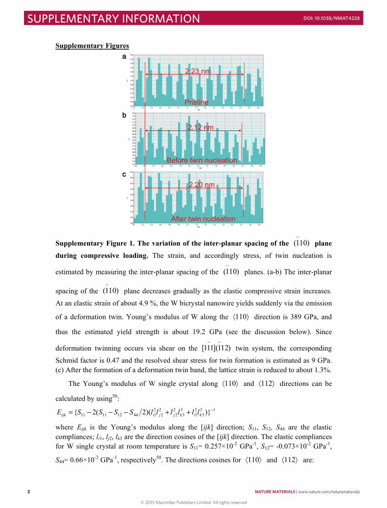
Supplementary Figure 1. The variation of the inter-planar spacing of the )101(−
plane
during compressive loading. The strain, and accordingly stress, of twin nucleation is
estimated by measuring the inter-planar spacing of the )101(−
planes. (a-b) The inter-planar
spacing of the )101(−
plane decreases gradually as the elastic compressive strain increases.
At an elastic strain of about 4.9 %, the W bicrystal nanowire yields suddenly via the emission
of a deformation twin. Young’s modulus of W along the 110 direction is 389 GPa, and
thus the estimated yield strength is about 19.2 GPa (see the discussion below). Since
deformation twinning occurs via shear on the )121](111[−−
twin system, the corresponding
Schmid factor is 0.47 and the resolved shear stress for twin formation is estimated as 9 GPa. (c) After the formation of a deformation twin band, the lattice strain is reduced to about 1.3%.
The Young’s modulus of W single crystal along 110 and 112 directions can be
calculated by using50:12
321
23
22
22
2144121111 )})(2(2{ −++−−−= kikjjiijk llllllSSSSE
where Eijk is the Young’s modulus along the [ijk] direction; S11, S12, S44 are the elastic compliances; li1, lj2, lk3 are the direction cosines of the [ijk] direction. The elastic compliances for W single crystal at room temperature is S11= 0.257×10⁻² GPa-1, S12= -0.073×10⁻² GPa-1,
S44= 0.66×10⁻² GPa-1, respectively50. The directions cosines for 110 and 112 are:
3
Direction cosines li1 lj2 lk3
110 2/2 2/2 0
112 6/1 6/1 6/2
Thus, Young’s moduli of W single crystal along 110 and 112 directions are calculated
to be E110 = E112 = 389 GPa. The yielding stress of different nanoscale W crystals is calculated by using εσ E= , where ε is the elastic strain just before yielding. The resolved shear stress on the shear plane can be obtained by using στ m= , where m is the Schmid factor on the corresponding slip systems, see Table 1 in the text.
© 2015 Macmillan Publishers Limited. All rights reserved
NATURE MATERIALS | www.nature.com/naturematerials 3
SUPPLEMENTARY INFORMATIONDOI: 10.1038/NMAT4228
2
Supplementary Figures
Supplementary Figure 1. The variation of the inter-planar spacing of the )101(−
plane
during compressive loading. The strain, and accordingly stress, of twin nucleation is
estimated by measuring the inter-planar spacing of the )101(−
planes. (a-b) The inter-planar
spacing of the )101(−
plane decreases gradually as the elastic compressive strain increases.
At an elastic strain of about 4.9 %, the W bicrystal nanowire yields suddenly via the emission
of a deformation twin. Young’s modulus of W along the 110 direction is 389 GPa, and
thus the estimated yield strength is about 19.2 GPa (see the discussion below). Since
deformation twinning occurs via shear on the )121](111[−−
twin system, the corresponding
Schmid factor is 0.47 and the resolved shear stress for twin formation is estimated as 9 GPa. (c) After the formation of a deformation twin band, the lattice strain is reduced to about 1.3%.
The Young’s modulus of W single crystal along 110 and 112 directions can be
calculated by using50:12
321
23
22
22
2144121111 )})(2(2{ −++−−−= kikjjiijk llllllSSSSE
where Eijk is the Young’s modulus along the [ijk] direction; S11, S12, S44 are the elastic compliances; li1, lj2, lk3 are the direction cosines of the [ijk] direction. The elastic compliances for W single crystal at room temperature is S11= 0.257×10⁻² GPa-1, S12= -0.073×10⁻² GPa-1,
S44= 0.66×10⁻² GPa-1, respectively50. The directions cosines for 110 and 112 are:
3
Direction cosines li1 lj2 lk3
110 2/2 2/2 0
112 6/1 6/1 6/2
Thus, Young’s moduli of W single crystal along 110 and 112 directions are calculated
to be E110 = E112 = 389 GPa. The yielding stress of different nanoscale W crystals is calculated by using εσ E= , where ε is the elastic strain just before yielding. The resolved shear stress on the shear plane can be obtained by using στ m= , where m is the Schmid factor on the corresponding slip systems, see Table 1 in the text.
© 2015 Macmillan Publishers Limited. All rights reserved

4 NATURE MATERIALS | www.nature.com/naturematerials
SUPPLEMENTARY INFORMATION DOI: 10.1038/NMAT4228
4
Supplementary Figure 2. The nucleation of deformation twins at the intersection between a grain boundary (GB) and free surface in a W bicrystal nanowire under compression. (a) Schematic of the crystallographic orientations of two adjoining grains in
the W bicrystal nanowire: the upper grain is loaded along ]111[ while the lower grain is
]101[ . (b) The pristine W bicrystal nanowire (15 nm in diameter). (c) Under compression,
deformation twins are observed to nucleate from both the GB (denoted as Twin 2) and the GB/surface intersection (denoted as Twin 1). (d-e) Twin 1 thickens layer-by-layer into both grains, while the thickening of Twin 2 mainly occurs inside Grain 2. Scale bars, 5 nm.
Supplementary Figure 3. MD simulations of twinning and detwinning mediated by a grain boundary in a W bicrystal nanowire. (a) A twin band (indicated by the red arrow) forms during compressive loading of the bicrystal nanowire, and (b) detwinning occurs upon unloading due to the deformation incompatibility at the intersection between the twin band and the grain boundary.
5
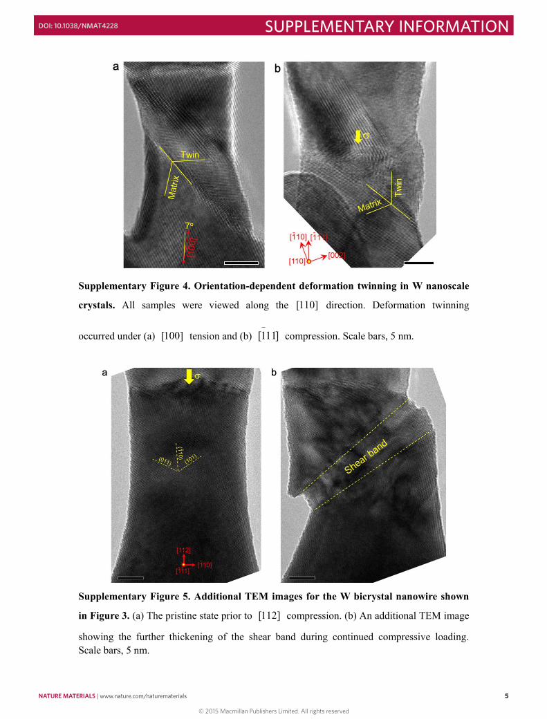
Supplementary Figure 4. Orientation-dependent deformation twinning in W nanoscale
crystals. All samples were viewed along the ]110[ direction. Deformation twinning
occurred under (a) ]100[ tension and (b) ]111[−
compression. Scale bars, 5 nm.
Supplementary Figure 5. Additional TEM images for the W bicrystal nanowire shown
in Figure 3. (a) The pristine state prior to ]112[ compression. (b) An additional TEM image
showing the further thickening of the shear band during continued compressive loading.Scale bars, 5 nm.
© 2015 Macmillan Publishers Limited. All rights reserved
NATURE MATERIALS | www.nature.com/naturematerials 5
SUPPLEMENTARY INFORMATIONDOI: 10.1038/NMAT4228
4
Supplementary Figure 2. The nucleation of deformation twins at the intersection between a grain boundary (GB) and free surface in a W bicrystal nanowire under compression. (a) Schematic of the crystallographic orientations of two adjoining grains in
the W bicrystal nanowire: the upper grain is loaded along ]111[ while the lower grain is
]101[ . (b) The pristine W bicrystal nanowire (15 nm in diameter). (c) Under compression,
deformation twins are observed to nucleate from both the GB (denoted as Twin 2) and the GB/surface intersection (denoted as Twin 1). (d-e) Twin 1 thickens layer-by-layer into both grains, while the thickening of Twin 2 mainly occurs inside Grain 2. Scale bars, 5 nm.
Supplementary Figure 3. MD simulations of twinning and detwinning mediated by a grain boundary in a W bicrystal nanowire. (a) A twin band (indicated by the red arrow) forms during compressive loading of the bicrystal nanowire, and (b) detwinning occurs upon unloading due to the deformation incompatibility at the intersection between the twin band and the grain boundary.
5
Supplementary Figure 4. Orientation-dependent deformation twinning in W nanoscale
crystals. All samples were viewed along the ]110[ direction. Deformation twinning
occurred under (a) ]100[ tension and (b) ]111[−
compression. Scale bars, 5 nm.
Supplementary Figure 5. Additional TEM images for the W bicrystal nanowire shown
in Figure 3. (a) The pristine state prior to ]112[ compression. (b) An additional TEM image
showing the further thickening of the shear band during continued compressive loading.Scale bars, 5 nm.
© 2015 Macmillan Publishers Limited. All rights reserved
6 NATURE MATERIALS | www.nature.com/naturematerials
SUPPLEMENTARY INFORMATION DOI: 10.1038/NMAT4228
6
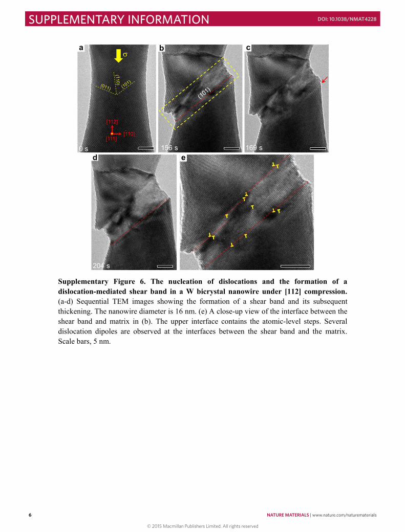
Supplementary Figure 6. The nucleation of dislocations and the formation of a dislocation-mediated shear band in a W bicrystal nanowire under [112] compression.(a-d) Sequential TEM images showing the formation of a shear band and its subsequent thickening. The nanowire diameter is 16 nm. (e) A close-up view of the interface between the shear band and matrix in (b). The upper interface contains the atomic-level steps. Several dislocation dipoles are observed at the interfaces between the shear band and the matrix. Scale bars, 5 nm.
7
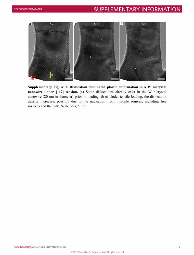
Supplementary Figure 7. Dislocation dominated plastic deformation in a W bicrystal nanowire under [112] tension. (a) Some dislocations already exist in the W bicrystal nanowire (20 nm in diameter) prior to loading. (b-c) Under tensile loading, the dislocation density increases, possibly due to the nucleation from multiple sources, including free surfaces and the bulk. Scale bars, 5 nm.
© 2015 Macmillan Publishers Limited. All rights reserved
NATURE MATERIALS | www.nature.com/naturematerials 7
SUPPLEMENTARY INFORMATIONDOI: 10.1038/NMAT4228
6
Supplementary Figure 6. The nucleation of dislocations and the formation of a dislocation-mediated shear band in a W bicrystal nanowire under [112] compression.(a-d) Sequential TEM images showing the formation of a shear band and its subsequent thickening. The nanowire diameter is 16 nm. (e) A close-up view of the interface between the shear band and matrix in (b). The upper interface contains the atomic-level steps. Several dislocation dipoles are observed at the interfaces between the shear band and the matrix. Scale bars, 5 nm.
7
Supplementary Figure 7. Dislocation dominated plastic deformation in a W bicrystal nanowire under [112] tension. (a) Some dislocations already exist in the W bicrystal nanowire (20 nm in diameter) prior to loading. (b-c) Under tensile loading, the dislocation density increases, possibly due to the nucleation from multiple sources, including free surfaces and the bulk. Scale bars, 5 nm.
© 2015 Macmillan Publishers Limited. All rights reserved
8 NATURE MATERIALS | www.nature.com/naturematerials
SUPPLEMENTARY INFORMATION DOI: 10.1038/NMAT4228
8
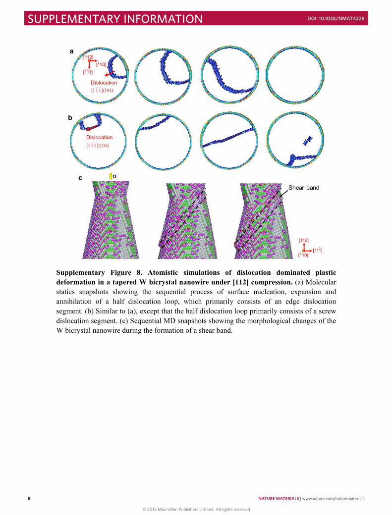
Supplementary Figure 8. Atomistic simulations of dislocation dominated plastic deformation in a tapered W bicrystal nanowire under [112] compression. (a) Molecular statics snapshots showing the sequential process of surface nucleation, expansion and annihilation of a half dislocation loop, which primarily consists of an edge dislocation segment. (b) Similar to (a), except that the half dislocation loop primarily consists of a screw dislocation segment. (c) Sequential MD snapshots showing the morphological changes of the W bicrystal nanowire during the formation of a shear band.
9
Supplementary Discussions
Supplementary Discussion 1. Analysis of the deformation twinning reported in nanocrystalline Ta
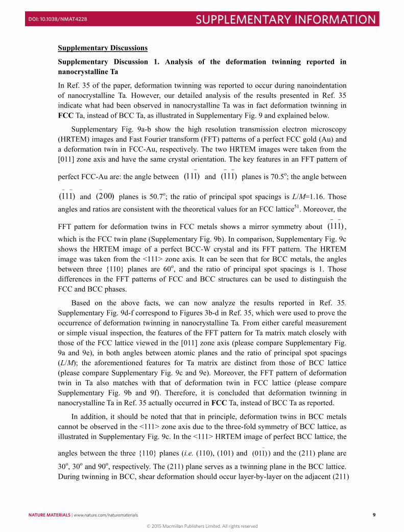
In Ref. 35 of the paper, deformation twinning was reported to occur during nanoindentation of nanocrystalline Ta. However, our detailed analysis of the results presented in Ref. 35 indicate what had been observed in nanocrystalline Ta was in fact deformation twinning in FCC Ta, instead of BCC Ta, as illustrated in Supplementary Fig. 9 and explained below.
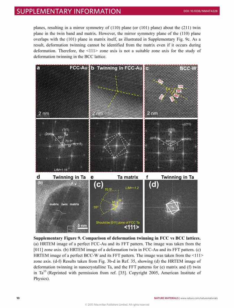
Supplementary Fig. 9a-b show the high resolution transmission electron microscopy (HRTEM) images and Fast Fourier transform (FFT) patterns of a perfect FCC gold (Au) and a deformation twin in FCC-Au, respectively. The two HRTEM images were taken from the [011] zone axis and have the same crystal orientation. The key features in an FFT pattern of
perfect FCC-Au are: the angle between )111(−
and )111(−−
planes is 70.5o; the angle between
)111(−−
and )002(−
planes is 50.7o; the ratio of principal spot spacings is L/M=1.16. Those angles and ratios are consistent with the theoretical values for an FCC lattice51. Moreover, the
FFT pattern for deformation twins in FCC metals shows a mirror symmetry about )111(−−
,which is the FCC twin plane (Supplementary Fig. 9b). In comparison, Supplementary Fig. 9c shows the HRTEM image of a perfect BCC-W crystal and its FFT pattern. The HRTEM image was taken from the <111> zone axis. It can be seen that for BCC metals, the angles between three {110} planes are 60o, and the ratio of principal spot spacings is 1. Those differences in the FFT patterns of FCC and BCC structures can be used to distinguish the FCC and BCC phases.
Based on the above facts, we can now analyze the results reported in Ref. 35.Supplementary Fig. 9d-f correspond to Figures 3b-d in Ref. 35, which were used to prove the occurrence of deformation twinning in nanocrystalline Ta. From either careful measurement or simple visual inspection, the features of the FFT pattern for Ta matrix match closely with those of the FCC lattice viewed in the [011] zone axis (please compare Supplementary Fig. 9a and 9e), in both angles between atomic planes and the ratio of principal spot spacings (L/M); the aforementioned features for Ta matrix are distinct from those of BCC lattice (please compare Supplementary Fig. 9c and 9e). Moreover, the FFT pattern of deformation twin in Ta also matches with that of deformation twin in FCC lattice (please compare Supplementary Fig. 9b and 9f). Therefore, it is concluded that deformation twinning in nanocrystalline Ta in Ref. 35 actually occurred in FCC Ta, instead of BCC Ta as reported.
In addition, it should be noted that that in principle, deformation twins in BCC metals cannot be observed in the <111> zone axis due to the three-fold symmetry of BCC lattice, as illustrated in Supplementary Fig. 9c. In the <111> HRTEM image of perfect BCC lattice, the
angles between the three {110} planes (i.e. (110), (101) and )101(−
) and the (211) plane are
30o, 30o and 90o, respectively. The (211) plane serves as a twinning plane in the BCC lattice. During twinning in BCC, shear deformation should occur layer-by-layer on the adjacent (211)
© 2015 Macmillan Publishers Limited. All rights reserved
NATURE MATERIALS | www.nature.com/naturematerials 9
SUPPLEMENTARY INFORMATIONDOI: 10.1038/NMAT4228
8
Supplementary Figure 8. Atomistic simulations of dislocation dominated plastic deformation in a tapered W bicrystal nanowire under [112] compression. (a) Molecular statics snapshots showing the sequential process of surface nucleation, expansion and annihilation of a half dislocation loop, which primarily consists of an edge dislocation segment. (b) Similar to (a), except that the half dislocation loop primarily consists of a screw dislocation segment. (c) Sequential MD snapshots showing the morphological changes of the W bicrystal nanowire during the formation of a shear band.
9
Supplementary Discussions
Supplementary Discussion 1. Analysis of the deformation twinning reported in nanocrystalline Ta
In Ref. 35 of the paper, deformation twinning was reported to occur during nanoindentation of nanocrystalline Ta. However, our detailed analysis of the results presented in Ref. 35 indicate what had been observed in nanocrystalline Ta was in fact deformation twinning in FCC Ta, instead of BCC Ta, as illustrated in Supplementary Fig. 9 and explained below.
Supplementary Fig. 9a-b show the high resolution transmission electron microscopy (HRTEM) images and Fast Fourier transform (FFT) patterns of a perfect FCC gold (Au) and a deformation twin in FCC-Au, respectively. The two HRTEM images were taken from the [011] zone axis and have the same crystal orientation. The key features in an FFT pattern of
perfect FCC-Au are: the angle between )111(−
and )111(−−
planes is 70.5o; the angle between
)111(−−
and )002(−
planes is 50.7o; the ratio of principal spot spacings is L/M=1.16. Those angles and ratios are consistent with the theoretical values for an FCC lattice51. Moreover, the
FFT pattern for deformation twins in FCC metals shows a mirror symmetry about )111(−−
,which is the FCC twin plane (Supplementary Fig. 9b). In comparison, Supplementary Fig. 9c shows the HRTEM image of a perfect BCC-W crystal and its FFT pattern. The HRTEM image was taken from the <111> zone axis. It can be seen that for BCC metals, the angles between three {110} planes are 60o, and the ratio of principal spot spacings is 1. Those differences in the FFT patterns of FCC and BCC structures can be used to distinguish the FCC and BCC phases.
Based on the above facts, we can now analyze the results reported in Ref. 35.Supplementary Fig. 9d-f correspond to Figures 3b-d in Ref. 35, which were used to prove the occurrence of deformation twinning in nanocrystalline Ta. From either careful measurement or simple visual inspection, the features of the FFT pattern for Ta matrix match closely with those of the FCC lattice viewed in the [011] zone axis (please compare Supplementary Fig. 9a and 9e), in both angles between atomic planes and the ratio of principal spot spacings (L/M); the aforementioned features for Ta matrix are distinct from those of BCC lattice (please compare Supplementary Fig. 9c and 9e). Moreover, the FFT pattern of deformation twin in Ta also matches with that of deformation twin in FCC lattice (please compare Supplementary Fig. 9b and 9f). Therefore, it is concluded that deformation twinning in nanocrystalline Ta in Ref. 35 actually occurred in FCC Ta, instead of BCC Ta as reported.
In addition, it should be noted that that in principle, deformation twins in BCC metals cannot be observed in the <111> zone axis due to the three-fold symmetry of BCC lattice, as illustrated in Supplementary Fig. 9c. In the <111> HRTEM image of perfect BCC lattice, the
angles between the three {110} planes (i.e. (110), (101) and )101(−
) and the (211) plane are
30o, 30o and 90o, respectively. The (211) plane serves as a twinning plane in the BCC lattice. During twinning in BCC, shear deformation should occur layer-by-layer on the adjacent (211)
© 2015 Macmillan Publishers Limited. All rights reserved
10 NATURE MATERIALS | www.nature.com/naturematerials
SUPPLEMENTARY INFORMATION DOI: 10.1038/NMAT4228
10
planes, resulting in a mirror symmetry of (110) plane (or (101) plane) about the (211) twin plane in the twin band and matrix. However, the mirror symmetry plane of the (110) plane overlaps with the (101) plane in matrix itself, as illustrated in Supplementary Fig. 9c. As a result, deformation twinning cannot be identified from the matrix even if it occurs during deformation. Therefore, the <111> zone axis is not a suitable zone axis for the study of deformation twinning in the BCC lattice.
Supplementary Figure 9. Comparison of deformation twinning in FCC vs BCC lattices. (a) HRTEM image of a perfect FCC-Au and its FFT pattern. The image was taken from the [011] zone axis. (b) HRTEM image of a deformation twin in FCC-Au and its FFT pattern. (c) HRTEM image of a perfect BCC-W and its FFT pattern. The image was taken from the <111> zone axis. (d-f) Results taken from Fig. 3b-d in Ref. 35, showing (d) the HRTEM image of deformation twinning in nanocrystalline Ta, and the FFT patterns for (e) matrix and (f) twin in Ta35 (Reprinted with permission from ref. [35]. Copyright 2005, American Institute of Physics).
11
Supplementary Discussion 2. Atomistic modelling of twin and dislocation nucleation for
110 compression
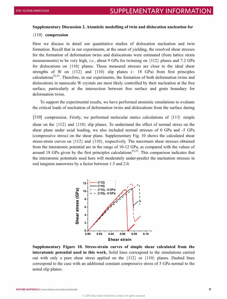
Here we discuss in detail our quantitative studies of dislocation nucleation and twin formation. Recall that in our experiments, at the onset of yielding, the resolved shear stresses for the formation of deformation twins and dislocations were estimated (from lattice strain measurements) to be very high, i.e., about 9 GPa for twinning on {112} planes and 7.2 GPa for dislocations on {110} planes. Those measured stresses are close to the ideal shear strengths of W on {112} and {110} slip planes (~ 18 GPa) from first principles calculations52,53. Therefore, in our experiments, the formation of both deformation twins and dislocations in nanoscale W crystals are most likely controlled by their nucleation at the free surface, particularly at the intersection between free surface and grain boundary for deformation twins.
To support the experimental results, we have performed atomistic simulations to evaluate the critical loads of nucleation of deformation twins and dislocations from the surface during
]101[−
compression. Firstly, we performed molecular statics calculations of 111 simple
shear on the {112} and {110} slip planes. To understand the effect of normal stress on the shear plane under axial loading, we also included normal stresses of 0 GPa and -5 GPa (compressive stress) on the shear plane. Supplementary Fig. 10 shows the calculated shear stress-strain curves on {112} and {110}, respectively. The maximum shear stresses obtained from the interatomic potential are in the range of 10-12 GPa, as compared with the values of around 18 GPa given by the first principles calculations52,53. This comparison indicates that the interatomic potentials used here will moderately under-predict the nucleation stresses in real tungsten nanowires by a factor between 1.5 and 2.0.
Supplementary Figure 10. Stress-strain curves of simple shear calculated from the interatomic potential used in this work. Solid lines correspond to the simulations carried out with only a pure shear stress applied on the {112} or {110} planes. Dashed lines correspond to the case with an additional constant compressive stress of 5 GPa normal to the noted slip planes.
© 2015 Macmillan Publishers Limited. All rights reserved
NATURE MATERIALS | www.nature.com/naturematerials 11
SUPPLEMENTARY INFORMATIONDOI: 10.1038/NMAT4228
10
planes, resulting in a mirror symmetry of (110) plane (or (101) plane) about the (211) twin plane in the twin band and matrix. However, the mirror symmetry plane of the (110) plane overlaps with the (101) plane in matrix itself, as illustrated in Supplementary Fig. 9c. As a result, deformation twinning cannot be identified from the matrix even if it occurs during deformation. Therefore, the <111> zone axis is not a suitable zone axis for the study of deformation twinning in the BCC lattice.
Supplementary Figure 9. Comparison of deformation twinning in FCC vs BCC lattices. (a) HRTEM image of a perfect FCC-Au and its FFT pattern. The image was taken from the [011] zone axis. (b) HRTEM image of a deformation twin in FCC-Au and its FFT pattern. (c) HRTEM image of a perfect BCC-W and its FFT pattern. The image was taken from the <111> zone axis. (d-f) Results taken from Fig. 3b-d in Ref. 35, showing (d) the HRTEM image of deformation twinning in nanocrystalline Ta, and the FFT patterns for (e) matrix and (f) twin in Ta35 (Reprinted with permission from ref. [35]. Copyright 2005, American Institute of Physics).
11
Supplementary Discussion 2. Atomistic modelling of twin and dislocation nucleation for
110 compression
Here we discuss in detail our quantitative studies of dislocation nucleation and twin formation. Recall that in our experiments, at the onset of yielding, the resolved shear stresses for the formation of deformation twins and dislocations were estimated (from lattice strain measurements) to be very high, i.e., about 9 GPa for twinning on {112} planes and 7.2 GPa for dislocations on {110} planes. Those measured stresses are close to the ideal shear strengths of W on {112} and {110} slip planes (~ 18 GPa) from first principles calculations52,53. Therefore, in our experiments, the formation of both deformation twins and dislocations in nanoscale W crystals are most likely controlled by their nucleation at the free surface, particularly at the intersection between free surface and grain boundary for deformation twins.
To support the experimental results, we have performed atomistic simulations to evaluate the critical loads of nucleation of deformation twins and dislocations from the surface during
]101[−
compression. Firstly, we performed molecular statics calculations of 111 simple
shear on the {112} and {110} slip planes. To understand the effect of normal stress on the shear plane under axial loading, we also included normal stresses of 0 GPa and -5 GPa (compressive stress) on the shear plane. Supplementary Fig. 10 shows the calculated shear stress-strain curves on {112} and {110}, respectively. The maximum shear stresses obtained from the interatomic potential are in the range of 10-12 GPa, as compared with the values of around 18 GPa given by the first principles calculations52,53. This comparison indicates that the interatomic potentials used here will moderately under-predict the nucleation stresses in real tungsten nanowires by a factor between 1.5 and 2.0.
Supplementary Figure 10. Stress-strain curves of simple shear calculated from the interatomic potential used in this work. Solid lines correspond to the simulations carried out with only a pure shear stress applied on the {112} or {110} planes. Dashed lines correspond to the case with an additional constant compressive stress of 5 GPa normal to the noted slip planes.
© 2015 Macmillan Publishers Limited. All rights reserved
12 NATURE MATERIALS | www.nature.com/naturematerials
SUPPLEMENTARY INFORMATION DOI: 10.1038/NMAT4228
12
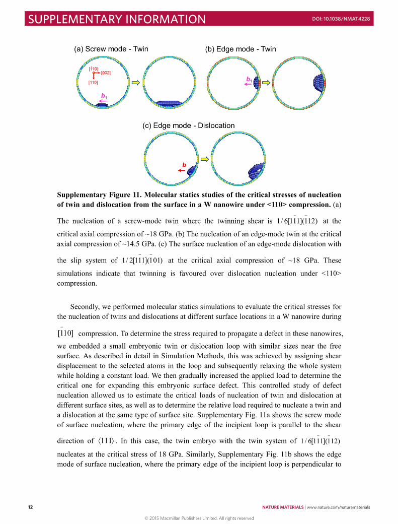
Supplementary Figure 11. Molecular statics studies of the critical stresses of nucleation of twin and dislocation from the surface in a W nanowire under <110> compression. (a)
The nucleation of a screw-mode twin where the twinning shear is )121](111[6/1−−
at the
critical axial compression of ~18 GPa. (b) The nucleation of an edge-mode twin at the critical axial compression of ~14.5 GPa. (c) The surface nucleation of an edge-mode dislocation with
the slip system of )011](111[2/1−−
at the critical axial compression of ~18 GPa. These
simulations indicate that twinning is favoured over dislocation nucleation under <110> compression.
Secondly, we performed molecular statics simulations to evaluate the critical stresses for the nucleation of twins and dislocations at different surface locations in a W nanowire during
]101[−
compression. To determine the stress required to propagate a defect in these nanowires,
we embedded a small embryonic twin or dislocation loop with similar sizes near the free surface. As described in detail in Simulation Methods, this was achieved by assigning shear displacement to the selected atoms in the loop and subsequently relaxing the whole system while holding a constant load. We then gradually increased the applied load to determine the critical one for expanding this embryonic surface defect. This controlled study of defect nucleation allowed us to estimate the critical loads of nucleation of twin and dislocation at different surface sites, as well as to determine the relative load required to nucleate a twin and a dislocation at the same type of surface site. Supplementary Fig. 11a shows the screw mode of surface nucleation, where the primary edge of the incipient loop is parallel to the shear
direction of 111 . In this case, the twin embryo with the twin system of )121](111[6/1−−
nucleates at the critical stress of 18 GPa. Similarly, Supplementary Fig. 11b shows the edge mode of surface nucleation, where the primary edge of the incipient loop is perpendicular to
13
the shear direction of 111 . In this case, an embryonic twin loop embedded on the {112}
shear plane generates the same type of twin product as (a) at the critical axial compression of about 14.5 GPa. In contrast, Supplementary Fig. 11c shows the nucleation of a surface defect on the {110} plane which, in this case, results in the nucleation of an edge dislocation. The
final product is a dislocation with the slip system of )011](111[2/1−−
at the critical axial
compression of ~18 GPa. These unit process studies give the critical axial loads of twin nucleation that are on the same order of magnitude as both experimental measurements and our MD results. Moreover, these simulations indicate that twinning is favoured over dislocation nucleation for <110> compression. Additionally, we note that the above studies focus on single crystals, but the intersection between free surface and grain boundary in bicrystals can create surface heterogeneities that facilitate the twin or dislocation nucleation, as shown in our MD simulations of bicrystals. However, the simulated critical loads for surface nucleation between single crystal and bicrystal setups are similar.
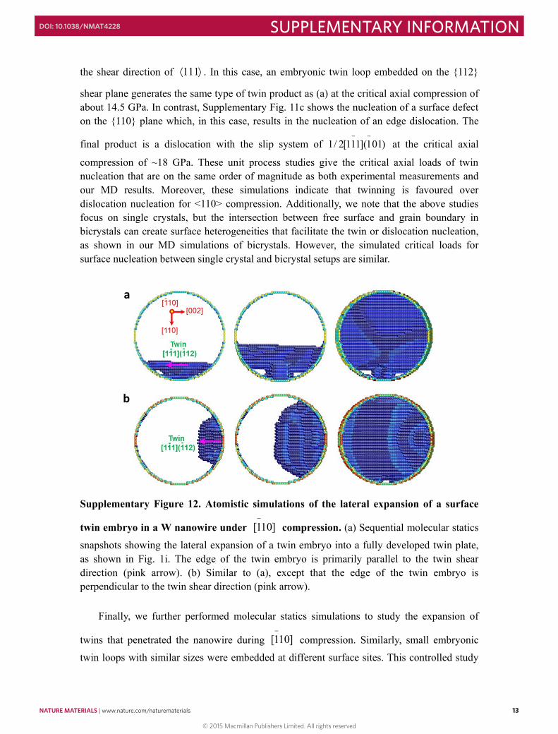
Supplementary Figure 12. Atomistic simulations of the lateral expansion of a surface
twin embryo in a W nanowire under ]101[−
compression. (a) Sequential molecular statics
snapshots showing the lateral expansion of a twin embryo into a fully developed twin plate, as shown in Fig. 1i. The edge of the twin embryo is primarily parallel to the twin shear direction (pink arrow). (b) Similar to (a), except that the edge of the twin embryo is perpendicular to the twin shear direction (pink arrow).
Finally, we further performed molecular statics simulations to study the expansion of
twins that penetrated the nanowire during ]101[−
compression. Similarly, small embryonic
twin loops with similar sizes were embedded at different surface sites. This controlled study
© 2015 Macmillan Publishers Limited. All rights reserved
NATURE MATERIALS | www.nature.com/naturematerials 13
SUPPLEMENTARY INFORMATIONDOI: 10.1038/NMAT4228
12
Supplementary Figure 11. Molecular statics studies of the critical stresses of nucleation of twin and dislocation from the surface in a W nanowire under <110> compression. (a)
The nucleation of a screw-mode twin where the twinning shear is )121](111[6/1−−
at the
critical axial compression of ~18 GPa. (b) The nucleation of an edge-mode twin at the critical axial compression of ~14.5 GPa. (c) The surface nucleation of an edge-mode dislocation with
the slip system of )011](111[2/1−−
at the critical axial compression of ~18 GPa. These
simulations indicate that twinning is favoured over dislocation nucleation under <110> compression.
Secondly, we performed molecular statics simulations to evaluate the critical stresses for the nucleation of twins and dislocations at different surface locations in a W nanowire during
]101[−
compression. To determine the stress required to propagate a defect in these nanowires,
we embedded a small embryonic twin or dislocation loop with similar sizes near the free surface. As described in detail in Simulation Methods, this was achieved by assigning shear displacement to the selected atoms in the loop and subsequently relaxing the whole system while holding a constant load. We then gradually increased the applied load to determine the critical one for expanding this embryonic surface defect. This controlled study of defect nucleation allowed us to estimate the critical loads of nucleation of twin and dislocation at different surface sites, as well as to determine the relative load required to nucleate a twin and a dislocation at the same type of surface site. Supplementary Fig. 11a shows the screw mode of surface nucleation, where the primary edge of the incipient loop is parallel to the shear
direction of 111 . In this case, the twin embryo with the twin system of )121](111[6/1−−
nucleates at the critical stress of 18 GPa. Similarly, Supplementary Fig. 11b shows the edge mode of surface nucleation, where the primary edge of the incipient loop is perpendicular to
13
the shear direction of 111 . In this case, an embryonic twin loop embedded on the {112}
shear plane generates the same type of twin product as (a) at the critical axial compression of about 14.5 GPa. In contrast, Supplementary Fig. 11c shows the nucleation of a surface defect on the {110} plane which, in this case, results in the nucleation of an edge dislocation. The
final product is a dislocation with the slip system of )011](111[2/1−−
at the critical axial
compression of ~18 GPa. These unit process studies give the critical axial loads of twin nucleation that are on the same order of magnitude as both experimental measurements and our MD results. Moreover, these simulations indicate that twinning is favoured over dislocation nucleation for <110> compression. Additionally, we note that the above studies focus on single crystals, but the intersection between free surface and grain boundary in bicrystals can create surface heterogeneities that facilitate the twin or dislocation nucleation, as shown in our MD simulations of bicrystals. However, the simulated critical loads for surface nucleation between single crystal and bicrystal setups are similar.
Supplementary Figure 12. Atomistic simulations of the lateral expansion of a surface
twin embryo in a W nanowire under ]101[−
compression. (a) Sequential molecular statics
snapshots showing the lateral expansion of a twin embryo into a fully developed twin plate, as shown in Fig. 1i. The edge of the twin embryo is primarily parallel to the twin shear direction (pink arrow). (b) Similar to (a), except that the edge of the twin embryo is perpendicular to the twin shear direction (pink arrow).
Finally, we further performed molecular statics simulations to study the expansion of
twins that penetrated the nanowire during ]101[−
compression. Similarly, small embryonic
twin loops with similar sizes were embedded at different surface sites. This controlled study
© 2015 Macmillan Publishers Limited. All rights reserved
14 NATURE MATERIALS | www.nature.com/naturematerials
SUPPLEMENTARY INFORMATION DOI: 10.1038/NMAT4228
14
allowed us to reveal the expansion behaviour of these twin embryos nucleated from different surface locations. Supplementary Fig. 12a shows the sequential molecular statics snapshots of expansion of a screw-type twin embryo, the edge of which is primarily parallel to the twin shear direction. During its nucleation process, this screw-type twin embryo can easily expand laterally, resulting in a complete twin plate, similar to the one shown in Fig. 1i. Similarly, Supplementary Fig. 12b shows the expansion of an edge-type twin embryo, resulting in a complete twin plate in the nanowire cross. The above molecular statics simulations demonstrate that a surface twin embryo can easily expand laterally to form a fully developed
twin band in a ]101[−
-oriented W nanowire after its nucleation from the favourable free
surface sites.
From the above modelling studies of surface nucleation and expansion of defects, we conclude that deformation twinning in nanoscale W crystals is controlled by surface nucleation, i.e., irrespective of types of surface sites and shear modes, a twin embryo can
nucleate from the free surface and expand into a twin band in a ]101[−
-oriented W nanowire
at the characteristic load level measured in experiments. Combining the results of twinning
under 110 compression (Supplementary Fig. 11-12) with the results of surface nucleation
of dislocations and twins under 112 compression (Figure 4 and Supplementary Fig. 8), we
demonstrate that deformation in nanoscale W crystals should be controlled by the competing nucleation mechanisms of twins and dislocations.
15
Supplementary Methods
1. Experimental Methods
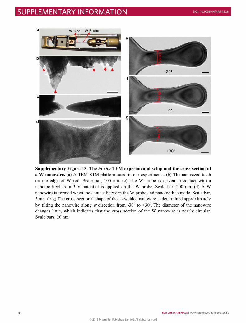
Polycrystalline W rods (99.98 wt.% purity, 0.010 inch in diameter), ordered from ESPI Metals Inc., were used for the experiments. The single crystal and bicrystal W nanowires were fabricated by a unique method of in situ welding of nanocrystals inside TEM. Theexperimental setup is illustrated in Supplementary Fig. 13. A FEI Tecnai F30 field emission gun (FEG) TEM equipped with a Nanofactory transmission electron microscopy(TEM)-scanning tunnelling microscope (STM) platform (Supplementary Fig. 13a) was used to study the deformation mechanisms in-situ. A W rod was fractured creating naturally occurring nanoscale-sized tooth-like projections (Supplementary Fig. 13b), which were subsequently used as one side of the platform. A W STM probe etched with NaOH solution was used as the other end of the platform. A 2-4 V potential was applied between the W probe and nanotooth, on either metallic rod or the probe side. When contact was made, the two tungsten crystals were welded together, forming either a single crystal or bicrystal nanowire (Supplementary Fig. 13c-d and Supplementary Movie 5) depending on the misorientation between the two crystals. Tilting of the sample shows that the cross section of W nanowires is nearly circular (Supplementary Fig. 13e-g). In-situ tension and compression experiments were conducted at room temperature by driving the W probe using a piezo-controller with a strain rate about 10-3 s-1. A CCD (charge-coupled device) camera was used to record the real-time images of deformation processes at 2 frames per second.
This in situ fabrication method enables the making of the clean sub-100 nm metallic nanostructures, which can involve different crystal orientations/types (e.g. FCC (Au, Pt) and BCC (Mo, V, Ta)) and dimensions. Considering the difficulties in handling and testing the nanomaterials, this method provides a relatively simple and novel approach to study the deformation mechanism of metallic nanomaterials, especially at the atomic scale. Moreover, this method may have potential applications in the assembly and interconnection of nanodevices.
© 2015 Macmillan Publishers Limited. All rights reserved
NATURE MATERIALS | www.nature.com/naturematerials 15
SUPPLEMENTARY INFORMATIONDOI: 10.1038/NMAT4228
14
allowed us to reveal the expansion behaviour of these twin embryos nucleated from different surface locations. Supplementary Fig. 12a shows the sequential molecular statics snapshots of expansion of a screw-type twin embryo, the edge of which is primarily parallel to the twin shear direction. During its nucleation process, this screw-type twin embryo can easily expand laterally, resulting in a complete twin plate, similar to the one shown in Fig. 1i. Similarly, Supplementary Fig. 12b shows the expansion of an edge-type twin embryo, resulting in a complete twin plate in the nanowire cross. The above molecular statics simulations demonstrate that a surface twin embryo can easily expand laterally to form a fully developed
twin band in a ]101[−
-oriented W nanowire after its nucleation from the favourable free
surface sites.
From the above modelling studies of surface nucleation and expansion of defects, we conclude that deformation twinning in nanoscale W crystals is controlled by surface nucleation, i.e., irrespective of types of surface sites and shear modes, a twin embryo can
nucleate from the free surface and expand into a twin band in a ]101[−
-oriented W nanowire
at the characteristic load level measured in experiments. Combining the results of twinning
under 110 compression (Supplementary Fig. 11-12) with the results of surface nucleation
of dislocations and twins under 112 compression (Figure 4 and Supplementary Fig. 8), we
demonstrate that deformation in nanoscale W crystals should be controlled by the competing nucleation mechanisms of twins and dislocations.
15
Supplementary Methods
1. Experimental Methods
Polycrystalline W rods (99.98 wt.% purity, 0.010 inch in diameter), ordered from ESPI Metals Inc., were used for the experiments. The single crystal and bicrystal W nanowires were fabricated by a unique method of in situ welding of nanocrystals inside TEM. Theexperimental setup is illustrated in Supplementary Fig. 13. A FEI Tecnai F30 field emission gun (FEG) TEM equipped with a Nanofactory transmission electron microscopy(TEM)-scanning tunnelling microscope (STM) platform (Supplementary Fig. 13a) was used to study the deformation mechanisms in-situ. A W rod was fractured creating naturally occurring nanoscale-sized tooth-like projections (Supplementary Fig. 13b), which were subsequently used as one side of the platform. A W STM probe etched with NaOH solution was used as the other end of the platform. A 2-4 V potential was applied between the W probe and nanotooth, on either metallic rod or the probe side. When contact was made, the two tungsten crystals were welded together, forming either a single crystal or bicrystal nanowire (Supplementary Fig. 13c-d and Supplementary Movie 5) depending on the misorientation between the two crystals. Tilting of the sample shows that the cross section of W nanowires is nearly circular (Supplementary Fig. 13e-g). In-situ tension and compression experiments were conducted at room temperature by driving the W probe using a piezo-controller with a strain rate about 10-3 s-1. A CCD (charge-coupled device) camera was used to record the real-time images of deformation processes at 2 frames per second.
This in situ fabrication method enables the making of the clean sub-100 nm metallic nanostructures, which can involve different crystal orientations/types (e.g. FCC (Au, Pt) and BCC (Mo, V, Ta)) and dimensions. Considering the difficulties in handling and testing the nanomaterials, this method provides a relatively simple and novel approach to study the deformation mechanism of metallic nanomaterials, especially at the atomic scale. Moreover, this method may have potential applications in the assembly and interconnection of nanodevices.
© 2015 Macmillan Publishers Limited. All rights reserved
16 NATURE MATERIALS | www.nature.com/naturematerials
SUPPLEMENTARY INFORMATION DOI: 10.1038/NMAT4228
16
Supplementary Figure 13. The in-situ TEM experimental setup and the cross section of a W nanowire. (a) A TEM-STM platform used in our experiments. (b) The nanosized teeth on the edge of W rod. Scale bar, 100 nm. (c) The W probe is driven to contact with a nanotooth where a 3 V potential is applied on the W probe. Scale bar, 200 nm. (d) A W nanowire is formed when the contact between the W probe and nanotooth is made. Scale bar, 5 nm. (e-g) The cross-sectional shape of the as-welded nanowire is determined approximately by tilting the nanowire along α direction from -30o to +30o. The diameter of the nanowire changes little, which indicates that the cross section of the W nanowire is nearly circular. Scale bars, 20 nm.
17
2. Simulation Methods
Molecular dynamics (MD) simulations. The simulations of twinning (Fig. 1), detwinning (Fig. 2) and dislocation mediated deformation (Supplementary Fig. 8c) in W nanowires were obtained by MD using LAMMPS. The temperature of the system was maintained at 300K and the time step was 1fs. The Ackland-Thetford-Finnis-Sinclair potential of W was used in
MD simulations. The applied strain rate was 108 s-1 for both ]101[−
and ]112[ compression.
All of the nanowires have circular cross sections. Some of the nanowires have uniform diameter along the nanowire length, while others were constructed by creating a tapered solid
of revolution about the nanowire axis. To create the bicrystal, a 111 and 110 oriented
single crystals (see Fig. 1k for complete orientations) were bonded through the nature of the interatomic cohesion.
Embedding a twin embryo in W nanowires. The twin embryo (Fig. 4 and Supplementary Fig. 11-12) in W nanowires was first created under constraints and then fully relaxed by molecular statics simulations using LAMMPS with the conjugate gradient (CG) algorithm. More specifically, to create a twin embryo, a pristine W nanowire was compressed to 4% so as to generate the internal stress to facilitate the twin formation. Then, a twin embryo was embedded into the nanowire through the following procedures: (a) A patch of five layers of
atoms in }112{ planes were selected near the side face of the nanowire. (b) Each layer of
atoms were moved by a prescribed displacement along the favoured twin shear direction as
follows: the displacement for the first layer was 11131 , the second was 11161 , the third
was 0, the forth was − 11161 and the fifth was − 11131 . (c) The nanowire was relaxed by
CG while the displaced atoms in the patch were constrained from moving. Under such constrained relaxation, an incipient twin embryo was formed in the nanowire. (d) After (c), the constraints on atoms in the patch were removed and the system was fully relaxed. As a
result, a twin embryo can be created in both the ]101[ and ]112[ nanowires.
© 2015 Macmillan Publishers Limited. All rights reserved
NATURE MATERIALS | www.nature.com/naturematerials 17
SUPPLEMENTARY INFORMATIONDOI: 10.1038/NMAT4228
16
Supplementary Figure 13. The in-situ TEM experimental setup and the cross section of a W nanowire. (a) A TEM-STM platform used in our experiments. (b) The nanosized teeth on the edge of W rod. Scale bar, 100 nm. (c) The W probe is driven to contact with a nanotooth where a 3 V potential is applied on the W probe. Scale bar, 200 nm. (d) A W nanowire is formed when the contact between the W probe and nanotooth is made. Scale bar, 5 nm. (e-g) The cross-sectional shape of the as-welded nanowire is determined approximately by tilting the nanowire along α direction from -30o to +30o. The diameter of the nanowire changes little, which indicates that the cross section of the W nanowire is nearly circular. Scale bars, 20 nm.
17
2. Simulation Methods
Molecular dynamics (MD) simulations. The simulations of twinning (Fig. 1), detwinning (Fig. 2) and dislocation mediated deformation (Supplementary Fig. 8c) in W nanowires were obtained by MD using LAMMPS. The temperature of the system was maintained at 300K and the time step was 1fs. The Ackland-Thetford-Finnis-Sinclair potential of W was used in
MD simulations. The applied strain rate was 108 s-1 for both ]101[−
and ]112[ compression.
All of the nanowires have circular cross sections. Some of the nanowires have uniform diameter along the nanowire length, while others were constructed by creating a tapered solid
of revolution about the nanowire axis. To create the bicrystal, a 111 and 110 oriented
single crystals (see Fig. 1k for complete orientations) were bonded through the nature of the interatomic cohesion.
Embedding a twin embryo in W nanowires. The twin embryo (Fig. 4 and Supplementary Fig. 11-12) in W nanowires was first created under constraints and then fully relaxed by molecular statics simulations using LAMMPS with the conjugate gradient (CG) algorithm. More specifically, to create a twin embryo, a pristine W nanowire was compressed to 4% so as to generate the internal stress to facilitate the twin formation. Then, a twin embryo was embedded into the nanowire through the following procedures: (a) A patch of five layers of
atoms in }112{ planes were selected near the side face of the nanowire. (b) Each layer of
atoms were moved by a prescribed displacement along the favoured twin shear direction as
follows: the displacement for the first layer was 11131 , the second was 11161 , the third
was 0, the forth was − 11161 and the fifth was − 11131 . (c) The nanowire was relaxed by
CG while the displaced atoms in the patch were constrained from moving. Under such constrained relaxation, an incipient twin embryo was formed in the nanowire. (d) After (c), the constraints on atoms in the patch were removed and the system was fully relaxed. As a
result, a twin embryo can be created in both the ]101[ and ]112[ nanowires.
© 2015 Macmillan Publishers Limited. All rights reserved
18 NATURE MATERIALS | www.nature.com/naturematerials
SUPPLEMENTARY INFORMATION DOI: 10.1038/NMAT4228
18
Supplementary Movies Captions
Supplementary Movie 1 The deformation of a W bicrystal nanowire under ]101[−
compression showing the nucleation and growth of a deformation twin. The movie was sped up 5 times.
Supplementary Movie 2 The nucleation of deformation twins from both the grain boundary and grain boundary/surface intersection in a W bicrystal nanowire under compression. The movie was sped up 5 times.
Supplementary Movie 3 The reversible deformation twinning in W bicrystal nanowire under
a 110 loading/unloading cycle. Under compressive loading, the W nanowire yields
through the nucleation and growth of a deformation twin. Detwinning occurs layer-by-layer when the loading is reversed, and the nanowire returns to its original shape without apparent defects after complete unloading. The movie was sped up 5 times.
Supplementary Movie 4 The nucleation of dislocations and subsequent shear band
formation in a W nanowire under ]112[ compression. A pristine W nanowire is viewed
along the ]111[ zone axis. Under compression, the plastic deformation of the W nanowire is
mediated by dislocation nucleation from multiple sources, including the free surface and the bulk. Further deformation results in the formation of a shear band, whose widening is mediated by dislocations both inside the band and at the band-matrix interface. The movie was sped up 10 times.
Supplementary Movie 5 The potential induced welding in W. A 3.3 V potential is applied on the nanotooth side. When the W probe touches the nanotooth, the two crystals are welded together by forming a bicrystal nanowire.
19
Supplementary References
50 Meyers, M. A. & Chawla, K. K. Mechanical Behavior of Materials. 2nd edn, (Cambridge University Press, 2009).
51 Williams, D. B. & Carter, C. B. The Transmission Electron Microscope. (Springer, 2009), p.299-301.
52 Roundy, D., Krenn, C. R., Cohen, M. L. & Morris, J. W. The ideal strength of tungsten. Philos. Mag. A 81, 1725-1747, (2001).
53 Ogata, S., Li, J., Hirosaki, N., Shibutani, Y. & Yip, S. Ideal shear strain of metals and ceramics. Phys. Rev. B 70, 104104, (2004).
© 2015 Macmillan Publishers Limited. All rights reserved

NATURE MATERIALS | www.nature.com/naturematerials 19
SUPPLEMENTARY INFORMATIONDOI: 10.1038/NMAT4228
18
Supplementary Movies Captions
Supplementary Movie 1 The deformation of a W bicrystal nanowire under ]101[−
compression showing the nucleation and growth of a deformation twin. The movie was sped up 5 times.
Supplementary Movie 2 The nucleation of deformation twins from both the grain boundary and grain boundary/surface intersection in a W bicrystal nanowire under compression. The movie was sped up 5 times.
Supplementary Movie 3 The reversible deformation twinning in W bicrystal nanowire under
a 110 loading/unloading cycle. Under compressive loading, the W nanowire yields
through the nucleation and growth of a deformation twin. Detwinning occurs layer-by-layer when the loading is reversed, and the nanowire returns to its original shape without apparent defects after complete unloading. The movie was sped up 5 times.
Supplementary Movie 4 The nucleation of dislocations and subsequent shear band
formation in a W nanowire under ]112[ compression. A pristine W nanowire is viewed
along the ]111[ zone axis. Under compression, the plastic deformation of the W nanowire is
mediated by dislocation nucleation from multiple sources, including the free surface and the bulk. Further deformation results in the formation of a shear band, whose widening is mediated by dislocations both inside the band and at the band-matrix interface. The movie was sped up 10 times.
Supplementary Movie 5 The potential induced welding in W. A 3.3 V potential is applied on the nanotooth side. When the W probe touches the nanotooth, the two crystals are welded together by forming a bicrystal nanowire.
19
Supplementary References
50 Meyers, M. A. & Chawla, K. K. Mechanical Behavior of Materials. 2nd edn, (Cambridge University Press, 2009).
51 Williams, D. B. & Carter, C. B. The Transmission Electron Microscope. (Springer, 2009), p.299-301.
52 Roundy, D., Krenn, C. R., Cohen, M. L. & Morris, J. W. The ideal strength of tungsten. Philos. Mag. A 81, 1725-1747, (2001).
53 Ogata, S., Li, J., Hirosaki, N., Shibutani, Y. & Yip, S. Ideal shear strain of metals and ceramics. Phys. Rev. B 70, 104104, (2004).
© 2015 Macmillan Publishers Limited. All rights reserved