groningen, the netherlands - media.nature.com · supplementary information. doi: 10.1038/nmat4423....
TRANSCRIPT
SUPPLEMENTARY INFORMATIONDOI: 10.1038/NMAT4423
NATURE MATERIALS | www.nature.com/naturematerials 1
Supplementary Information
The negative piezoelectric effect of the ferroelectric polymer
poly(vinylidene-fluoride)
By Ilias Katsouras1,2, Kamal Asadi1, Mengyuan Li (李梦媛)3,4, Tim B. van Driel5, Kasper S.
Kjær5, Dong Zhao (赵冬)1, Thomas Lenz1, Yun Gu (顾 韵)5, Paul W.M. Blom1, Dragan
Damjanovic6, Martin M. Nielsen5 and Dago M. de Leeuw1,7*
1Max-Planck Institute for Polymer Research, Ackermannweg 10, 55128 Mainz, Germany2Holst Centre, High Tech Campus 31, 5656 AE, Eindhoven, The Netherlands3 Zernike Institute for Advanced Materials, University of Groningen, Nijenborgh 4, 9747 AG,
Groningen, The Netherlands4 Electronic Information Industry, CCID Thinktank, China Center for Information Industry
Development No.27 Wanshou Road, 100846, Beijing, China5Department of Physics, Technical University of Denmark, Copenhagen, Denmark 6Ceramics
Laboratory, Swiss Federal Institute of Technology – EPFL, 1015 Lausanne, Switzerland7King Abdulaziz University, Abdullah Sulayman, 22254 Jeddah, Saudi Arabia
[*] E-mail: [email protected]
1
The negative piezoelectric effect of the ferroelectric polymer poly(vinylidene fluoride)
© 2015 Macmillan Publishers Limited. All rights reserved
2 NATURE MATERIALS | www.nature.com/naturematerials
SUPPLEMENTARY INFORMATION DOI: 10.1038/NMAT4423
Table of Contents
1. Supplementary Introduction 3
2. Dimensional model 3
3. Capacitor fabrication and characterization 4
4. Crystal structure of P(VDF-TrFE) 5
5. Microstructure of PVDF and P(VDF-TrFE) 6
6. Dynamic in-situ X-ray measurements and data acquisition 7
7. Data synchronization 9
8. Clamping and capacitor layout considerations 11
9. Parameter extraction 13
9.1 Modeling ferroelectric D-E hysteresis loops
9.2 Parity function
9.3 Normalization of strain
10. Data series of P(VDF-TrFE) 15
10.1 Amplitude series
10.2 Frequency series
10.3 Determination of d33 at low electric field
11. Modeling of reported strain measurements on β-PVDF 18
12. Variation of extracted piezoelectric coefficients with microstructure 21
References 27
2
© 2015 Macmillan Publishers Limited. All rights reserved
NATURE MATERIALS | www.nature.com/naturematerials 3
SUPPLEMENTARY INFORMATIONDOI: 10.1038/NMAT4423
1. Supplementary Introduction
The first section of this Supplementary Information contains a detailed description of the dimensional model that is commonly used to explain the negative piezoelectric effect in ferroelectric polymers. Sections 3-5 contain the experimental details about capacitor fabrication and characterization of the microstructure of the P(VDF-TrFE) films by X-ray diffraction measurements, SEM and atomic force microscopy. Subsequently, in sections 6 and 7 the experimental details for the dynamic in-situ X-ray measurements are presented, and the data acquisition and synchronization are discussed. In section 8 we show that clamping effects can be ignored. In section 9 we present the extraction of piezoelectric coefficients from the strain data. The empirical model that has been previously used to quantitatively describe the polarization as a function of electric field in ferroelectric capacitors is discussed. To take into account that the sign of the strain depends on the relative orientation of electric field and polarization we introduce a parity function, ṕ. The consequences are discussed. The strain is normalized to zero at zero electric field. The justification is presented. Section 10 contains an overview of all measurements, where the frequency and amplitude of the driving signal were varied systematically. The data sets and fits, as well as the extracted parameters, are presented. For completeness, X-ray measurements at low electric field are included. In section 11 we analyze reported strain measurements on ferroelectric β-PVDF films. In section 12 wediscuss the relation between piezoelectric coefficients and ferroelectric properties as extracted for thick films, where we varied the microstructure by varying the annealing temperature.
2. Dimensional model
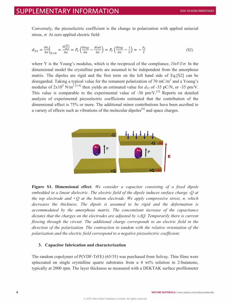
Various mechanisms have been proposed to explain the negative piezoelectric effect in PVDF and its copolymers. A commonly used explanation is the “dimensional effect”, which assumes that the dipoles are rigid and retain their fixed moment and orientation during mechanical deformation.[1,2,3] PVDF is a semi-crystalline polymer with a crystallinity of about 50%. Piezoelectricity is then assumed to be due to a change in volume of the amorphous part of the sample. The dimensional model basically describes the displacement of surface electrodes in the fields of fixed dipole moments of polar crystals, as schematically depicted in Fig. S1.
The magnitude of the piezoelectric effect can be estimated as follows. We apply an electric field, E, perpendicular to a thin P(VDF-TrFE) film sandwiched between two electrodes. The electric field is parallel to the poling direction. The relative change in film thickness, the longitudinal strain S33, is then given by:
𝑆𝑆𝑆𝑆33 = 𝑑𝑑𝑑𝑑33𝐸𝐸𝐸𝐸 (S1)
where d33 is the linear, longitudinal piezoelectric coefficient. The film exhibits a spontaneous polarization Ps, equal to the macroscopic dipole moment, µ, over the sample volume, V.
3
© 2015 Macmillan Publishers Limited. All rights reserved
4 NATURE MATERIALS | www.nature.com/naturematerials
SUPPLEMENTARY INFORMATION DOI: 10.1038/NMAT4423
Conversely, the piezoelectric coefficient is the change in polarization with applied uniaxial stress, σ. Αt zero applied electric field:
𝑑𝑑𝑑𝑑33 = 𝜕𝜕𝜕𝜕𝜕𝜕𝜕𝜕𝑠𝑠𝑠𝑠𝜕𝜕𝜕𝜕𝜕𝜕𝜕𝜕�𝐸𝐸𝐸𝐸=0
=𝜕𝜕𝜕𝜕�𝜇𝜇𝜇𝜇𝑉𝑉𝑉𝑉�
𝜕𝜕𝜕𝜕𝜕𝜕𝜕𝜕= 𝑃𝑃𝑃𝑃𝑟𝑟𝑟𝑟 �
𝜕𝜕𝜕𝜕𝜕𝜕𝜕𝜕𝜕𝜕𝜕𝜕𝜇𝜇𝜇𝜇𝜕𝜕𝜕𝜕𝜕𝜕𝜕𝜕
− 𝜕𝜕𝜕𝜕𝜕𝜕𝜕𝜕𝜕𝜕𝜕𝜕𝑉𝑉𝑉𝑉𝜕𝜕𝜕𝜕𝜕𝜕𝜕𝜕
� = 𝑃𝑃𝑃𝑃𝑟𝑟𝑟𝑟 �𝜕𝜕𝜕𝜕𝜕𝜕𝜕𝜕𝜕𝜕𝜕𝜕𝜇𝜇𝜇𝜇𝜕𝜕𝜕𝜕𝜕𝜕𝜕𝜕
− 1𝑌𝑌𝑌𝑌� ≈ − 𝜕𝜕𝜕𝜕𝑟𝑟𝑟𝑟
𝑌𝑌𝑌𝑌 (S2)
where Y is the Young’s modulus, which is the reciprocal of the compliance, ∂lnV/∂σ. In the dimensional model the crystalline parts are assumed to be independent from the amorphous matrix. The dipoles are rigid and the first term on the left hand side of Eq.[S2] can be disregarded. Taking a typical value for the remanent polarization of 70 mC/m2 and a Young’s modulus of 2x10⁹ N/m2 [3,4] then yields an estimated value for d33 of -35 pC/N, or -35 pm/V. This value is comparable to the experimental value of -30 pm/V.[5] Reports on detailed analysis of experimental piezoelectric coefficients estimated that the contribution of the dimensional effect is 75% or more. The additional minor contributions have been ascribed to a variety of effects such as vibrations of the molecular dipoles[6] and space charges.
Figure S1. Dimensional effect. We consider a capacitor consisting of a fixed dipole embedded in a linear dielectric. The electric field of the dipole induces surface charge -Q at the top electrode and +Q at the bottom electrode. We apply compressive stress, σ, which decreases the thickness. The dipole is assumed to be rigid and the deformation is accommodated by the amorphous matrix. The concomitant increase of the capacitance dictates that the charges on the electrodes are adjusted by ±ΔQ. Temporarily there is current flowing through the circuit. The additional charge corresponds to an electric field in the direction of the polarization. The contraction in tandem with the relative orientation of the polarization and the electric field correspond to a negative piezoelectric coefficient.
3. Capacitor fabrication and characterization
The random copolymer of P(VDF-TrFE) (65/35) was purchased from Solvay. Thin films were spincoated on single crystalline quartz substrates from a 4 wt% solution in 2-butanone, typically at 2000 rpm. The layer thickness as measured with a DEKTAK surface profilometer
4
© 2015 Macmillan Publishers Limited. All rights reserved
NATURE MATERIALS | www.nature.com/naturematerials 5
SUPPLEMENTARY INFORMATIONDOI: 10.1038/NMAT4423
amounted to 450 nm. The layers were then annealed for 2 hours in vacuum at 140 oC to enhance the ferroelectric properties. As a bottom electrode we used Pd, with 2 nm Cr as an adhesion layer. Au cannot be used due to interference of its X-ray diffraction pattern with that of P(VDF-TrFE). To allow in-situ grazing incidence X-ray diffraction measurements (GI-XRD), large device areas of 1 cm2 were fabricated. As a top electrode we used a thin film of the amorphous conducting polymer PEDOT:PSS, a water-based suspension of poly(3,4-ethylenedioxythiophene) stabilized with poly(4-styrenesulphonic acid) (AGFA ICP 1020 (Agfa-Gevaert). To prevent dewetting a few drops of the nonionic Zonyl FSO-100 (DuPont) fluoro-surfactant were added to the solution. The PEDOT:PSS layer thickness amounted to 100 nm and the conductivity amounted to 300 S/cm. Finally, the redundant PEDOT:PSS was removed by reactive ion etching using a shadow mask.
Electric displacement loops versus electric field for the capacitors were measured using a Sawyer-Tower circuit, consisting of a Tektronix AFG3102 function generator, a LeCroy waveRunner 204Xi 2GHz oscilloscope and a Krohn-Hite 7600 wide-band amplifier. The capacitors were measured with a continuous triangular wave signal, with a frequency between 1 Hz and 100 Hz, using a reference capacitor of 1μF.
4. Crystal structure of P(VDF-TrFE)
Grazing incidence X-ray diffraction (GI-XRD), was used to study the crystal structure of P(VDF-TrFE). The homopolymer PVDF tends to crystallize in the thermodynamically stable α structure. This polymorph is paraelectric. The presence of the TrFE monomers in the random copolymer P(VDF-TrFE) destabilizes the α structure. Instead, the copolymers crystallize in a structure resembling the ferroelectric β-phase of PVDF. Thin P(VDF-TrFE) films appear to contain two phases after deposition. These phases resemble the α- and β-forms of the homopolymer PVDF. After annealing at 140°C, where a non-ferroelectric high temperature (HT) phase is formed, and subsequent cooling to room temperature, only the β-type phase remains. Two modifications of this phase have been described in literature, called the ‘cooled phase’ (CL) and the “low temperature phase” (LT), both found in bulk material.
Table S1. Crystallographic data of several PVDF and P(VDF-TrFE) phases. The data are compiled from “Ferroelectric Polymers, chemistry, physics and applications” edited by Hari Singh Nalwa.[7]
Phase Conditions Structure Chain A b c βHT P(VDF-TrFE) 55/45, 80°C orthorhombic Random 9.75 Å 5.63 Å 4.60 Å ---LT P(VDF-TrFE) 55/45 monoclinic all T 9.12 Å 5.25 Å 2.55 Å 93°
CLP(VDF-TrFE) 55/45
monoclinicmostly
T9.16 Å 5.43 Å 2.53Å 93°
P(VDF-TrFE) 37/63 9.37 Å 5.52 Å 2.53 Å 93°I / β PVDF Cm2m (38) all T 8.58 Å 4.91 Å 2.56 Å ---IΙ/ α PVDF P21/c (14) TGT-G 4.96 Å 9.64 Å 4.62 Å 90°
5
© 2015 Macmillan Publishers Limited. All rights reserved
6 NATURE MATERIALS | www.nature.com/naturematerials
SUPPLEMENTARY INFORMATION DOI: 10.1038/NMAT4423
Pure PTrFE is supposed to have a structure very similar to the P(VDF-TrFE) CL phase. This phase consists of small domains of all trans chains bordered by single gauche bonds. These gauche bonds slightly change the unit cell parameters, compared to the LT phase. The chains will be wider and shorter, resulting in an increase in a- and b- axes and a decrease in c axis. Furthermore, the LT phase is pseudohexagonal (a/b = √3), resulting in a combined 1.1.0 / 2.0.0 diffraction peak. For the CL phase a/b < √3, therefore the 1.1.0 and 2.0.0 peaks do not coincide. These peaks are also wide, caused by the small domain size, typical for the CL phase.
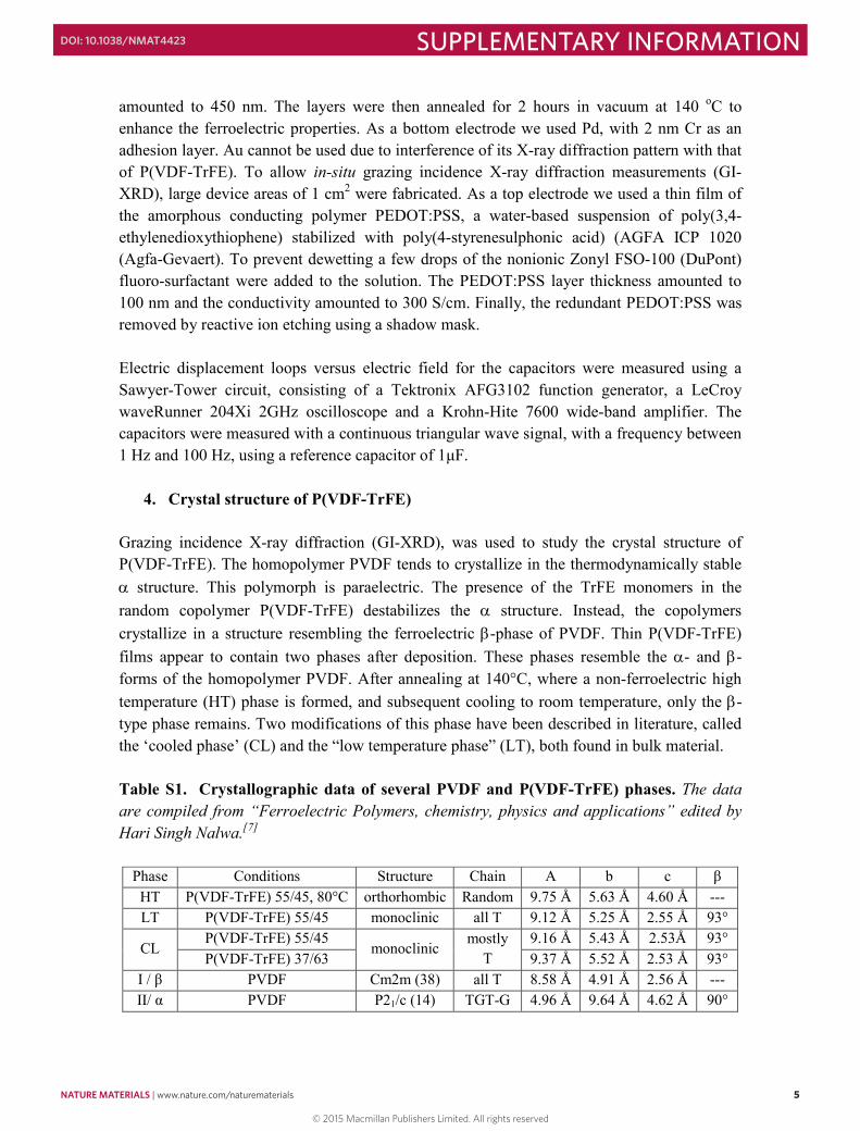
Specular XRD measurements on a series of PTrFE and P(VDF-TrFE) thin films are presented in Fig. S2. After annealing at 140°C only the LT phase is present for all investigated compositions. Only a single diffraction peak of the combined 1.1.0/2.0.0 diffraction is visible. The peak is relatively sharp. The inset shows the peak position as a function of composition. The trendline gives the combined d spacing for samples with 50% VDF or more. In the dynamic in-situ measurements we used P(VDF-TrFE) (65/35). This polymer crystallizes in pseudo-hexagonal LT phase with unit cell parameters of a = 9.04 Å, b = 5.22 Å, c = 2.55 Åand β = 93°.
Figure S2. Specular XRD measurements of PTrFE and P(VDF-TrFE). The (110)/(200)diffraction peak of P(VDF-TrFE) films is presented for different compositions. The inset shows the peak position as a function of composition. The trend line gives the combined d spacing for samples with 50% VDF or more.
5. Microstructure of PVDF and P(VDF-TrFE)
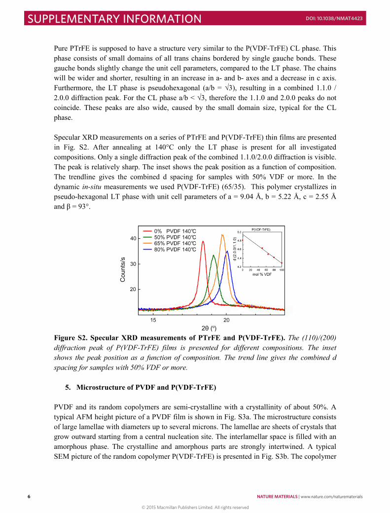
PVDF and its random copolymers are semi-crystalline with a crystallinity of about 50%. A typical AFM height picture of a PVDF film is shown in Fig. S3a. The microstructure consists of large lamellae with diameters up to several microns. The lamellae are sheets of crystals that grow outward starting from a central nucleation site. The interlamellar space is filled with an amorphous phase. The crystalline and amorphous parts are strongly intertwined. A typical SEM picture of the random copolymer P(VDF-TrFE) is presented in Fig. S3b. The copolymer
6
© 2015 Macmillan Publishers Limited. All rights reserved
NATURE MATERIALS | www.nature.com/naturematerials 7
SUPPLEMENTARY INFORMATIONDOI: 10.1038/NMAT4423
crystallizes in small needle like-domains. Details of the packing and folding of the polymer chains are not completely known but, as in PVDF, the amorphous and crystalline phases appear to be intermixed.
Figure S3. Microstructure of PVDF and P(VDF-TrFE). (a) A typical AFM height image of a PVDF film with a thickness of 117 nm. (b) SEM image of a 500 nm-thick P(VDF-TrFE) film spincoated on a quartz substrate. The scan sizes are indicated by the respective scale bars.
6. Dynamic in-situ X-ray measurements and data acquisition
In-situ grazing incidence X-ray diffraction measurements (GI-XRD) were conducted on the purpose-built, large-area capacitors described in Section 3. Measurements were performed on samples aligned in the high precision 6-circle diffractometer installed at the High Resolution Diffraction Beamline P08 at PETRAIII, Deutsches Elektron Synchrotron (DESY), Hamburg. The 25 keV X-ray beam was focused at the sample position with a compound refractive lens, and the beam size at the sample was set to 50x500 µm by a set of slits. The incidence angle on the sample was set to 0.25o, matching the X-ray footprint to the active area of the device. A Cyberstar scintillation detector was used to align samples in the specular geometry, after which the time-resolved data was measured on a Pilatus 100K area pixel detector placed at 2 m distance to the sample, collecting the out-of-plane scattering between angles of 2θ = 5.4o
and 2θ = 6.5o in the specular plane, corresponding to wave vector transfer of 1.19 Å-1 and 1.44 Å-1, respectively.
A triangular waveform was used to drive the ferroelectric capacitors. The amplitude and the frequency of the triangular driving waveform were varied. The applied AC voltage and the capacitor response were recorded as a function of time using an oscilloscope in a Sawyer-Tower configuration. The circuit consisted of a Tektronix AFG3102 function generatorconnected to a Krohn-Hite 7600 wide-band amplifier, monitored by a LeCroy waveRunner 204Xi 2GHz oscilloscope. The displacement of the ferroelectric capacitor was determined by monitoring the voltage drop over a large (1μF) reference linear capacitor in series.
A TTL trigger signal was generated at the (negative-to-positive) zero-crossing of the driving voltage by a Highland P400 delay and pulse generator. The trigger pulse was sent to the
7
© 2015 Macmillan Publishers Limited. All rights reserved
8 NATURE MATERIALS | www.nature.com/naturematerials
SUPPLEMENTARY INFORMATION DOI: 10.1038/NMAT4423
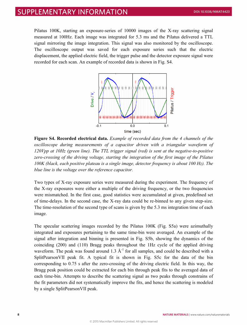
Pilatus 100K, starting an exposure-series of 10000 images of the X-ray scattering signalmeasured at 100Hz. Each image was integrated for 5.3 ms and the Pilatus delivered a TTL signal mirroring the image integration. This signal was also monitored by the oscilloscope. The oscilloscope output was saved for each exposure series such that the electricdisplacement, the applied electric field, the trigger pulse and the detector exposure signal wererecorded for each scan. An example of recorded data is shown in Fig. S4.
Figure S4. Recorded electrical data. Example of recorded data from the 4 channels of the oscilloscope during measurements of a capacitor driven with a triangular waveform of 120Vpp at 10Hz (green line). The TTL trigger signal (red) is sent at the negative-to-positive zero-crossing of the driving voltage, starting the integration of the first image of the Pilatus 100K (black, each positive plateau is a single image, detector frequency is about 100 Hz). The blue line is the voltage over the reference capacitor.
Two types of X-ray exposure series were measured during the experiment. The frequency of the X-ray exposures were either a multiple of the driving frequency, or the two frequencies were mismatched. In the first case, good statistics were accumulated at given, predefined set of time-delays. In the second case, the X-ray data could be re-binned to any given step-size. The time-resolution of the second type of scans is given by the 5.3 ms integration time of each image.
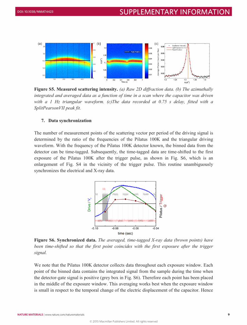
The specular scattering images recorded by the Pilatus 100K (Fig. S5a) were azimuthally integrated and exposures pertaining to the same time-bin were averaged. An example of the signal after integration and binning is presented in Fig. S5b, showing the dynamics of the coinciding (200) and (110) Bragg peaks throughout the 1Hz cycle of the applied driving waveform. The peak was found around 1.3 Å-1 for all samples, and could be described with a SplitPearsonVII peak fit. A typical fit is shown in Fig. S5c for the data of the bin corresponding to 0.75 s after the zero-crossing of the driving electric field. In this way, the Bragg peak position could be extracted for each bin through peak fits to the averaged data of each time-bin. Attempts to describe the scattering signal as two peaks through constrains of the fit parameters did not systematically improve the fits, and hence the scattering is modeled by a single SplitPearsonVII peak.
8
© 2015 Macmillan Publishers Limited. All rights reserved
NATURE MATERIALS | www.nature.com/naturematerials 9
SUPPLEMENTARY INFORMATIONDOI: 10.1038/NMAT4423
Figure S5. Measured scattering intensity. (a) Raw 2D diffraction data. (b) The azimuthally integrated and averaged data as a function of time in a scan where the capacitor was driven with a 1 Hz triangular waveform. (c)The data recorded at 0.75 s delay, fitted with a SplitPearsonVII peak fit.
7. Data synchronization
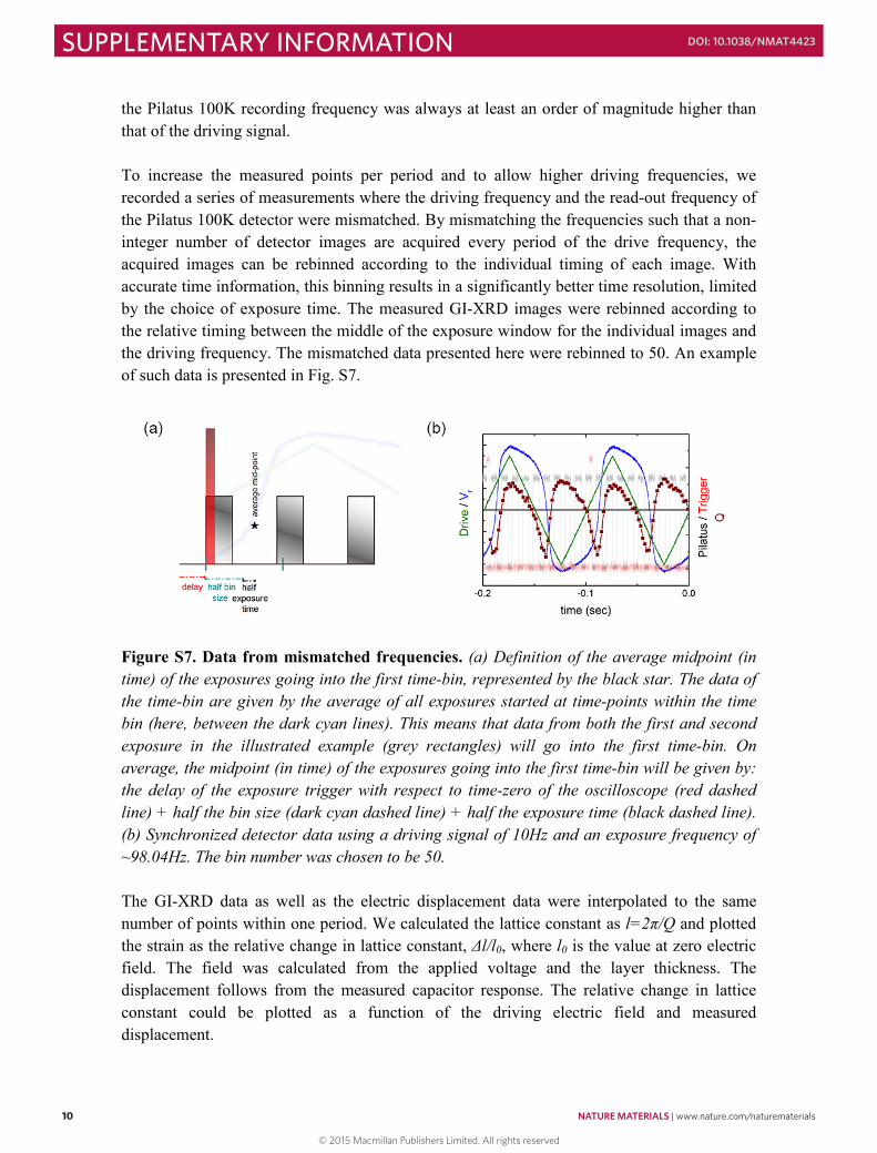
The number of measurement points of the scattering vector per period of the driving signal is determined by the ratio of the frequencies of the Pilatus 100K and the triangular driving waveform. With the frequency of the Pilatus 100K detector known, the binned data from the detector can be time-tagged. Subsequently, the time-tagged data are time-shifted to the first exposure of the Pilatus 100K after the trigger pulse, as shown in Fig. S6, which is an enlargement of Fig. S4 in the vicinity of the trigger pulse. This routine unambiguously synchronizes the electrical and X-ray data.
Figure S6. Synchronized data. The averaged, time-tagged X-ray data (brown points) have been time-shifted so that the first point coincides with the first exposure after the trigger signal.
We note that the Pilatus 100K detector collects data throughout each exposure window. Each point of the binned data contains the integrated signal from the sample during the time when the detector-gate signal is positive (grey box in Fig. S6). Therefore each point has been placed in the middle of the exposure window. This averaging works best when the exposure window is small in respect to the temporal change of the electric displacement of the capacitor. Hence
9
© 2015 Macmillan Publishers Limited. All rights reserved
10 NATURE MATERIALS | www.nature.com/naturematerials
SUPPLEMENTARY INFORMATION DOI: 10.1038/NMAT4423
the Pilatus 100K recording frequency was always at least an order of magnitude higher than that of the driving signal.
To increase the measured points per period and to allow higher driving frequencies, we recorded a series of measurements where the driving frequency and the read-out frequency of the Pilatus 100K detector were mismatched. By mismatching the frequencies such that a non-integer number of detector images are acquired every period of the drive frequency, the acquired images can be rebinned according to the individual timing of each image. With accurate time information, this binning results in a significantly better time resolution, limited by the choice of exposure time. The measured GI-XRD images were rebinned according to the relative timing between the middle of the exposure window for the individual images and the driving frequency. The mismatched data presented here were rebinned to 50. An example of such data is presented in Fig. S7.
Figure S7. Data from mismatched frequencies. (a) Definition of the average midpoint (in time) of the exposures going into the first time-bin, represented by the black star. The data of the time-bin are given by the average of all exposures started at time-points within the time bin (here, between the dark cyan lines). This means that data from both the first and second exposure in the illustrated example (grey rectangles) will go into the first time-bin. On average, the midpoint (in time) of the exposures going into the first time-bin will be given by: the delay of the exposure trigger with respect to time-zero of the oscilloscope (red dashed line) + half the bin size (dark cyan dashed line) + half the exposure time (black dashed line). (b) Synchronized detector data using a driving signal of 10Hz and an exposure frequency of~98.04Hz. The bin number was chosen to be 50.
The GI-XRD data as well as the electric displacement data were interpolated to the same number of points within one period. We calculated the lattice constant as l=2π/Q and plotted the strain as the relative change in lattice constant, Δl/l0, where l0 is the value at zero electric field. The field was calculated from the applied voltage and the layer thickness. The displacement follows from the measured capacitor response. The relative change in lattice constant could be plotted as a function of the driving electric field and measured displacement.
10
© 2015 Macmillan Publishers Limited. All rights reserved
NATURE MATERIALS | www.nature.com/naturematerials 11
SUPPLEMENTARY INFORMATIONDOI: 10.1038/NMAT4423
8. Clamping and capacitor layout considerations
The lateral dimensions of a ferroelectric thin film can be constrained by the substrate. In the case of total clamping, the in-plane strain induced by an electric field across the capacitor should be zero; there is no change in the lateral dimensions of the film when an electric field is applied. As a result, in a clamped film the measured piezoelectric coefficient is reduced in respect to the bulk. The effective longitudinal piezoelectric coefficient is:
𝑑𝑑𝑑𝑑33𝑒𝑒𝑒𝑒𝑒𝑒𝑒𝑒𝑒𝑒𝑒𝑒 = 𝑑𝑑𝑑𝑑33 −
2𝑑𝑑𝑑𝑑31𝑠𝑠𝑠𝑠13𝑓𝑓𝑓𝑓
𝑠𝑠𝑠𝑠11𝑓𝑓𝑓𝑓 +𝑠𝑠𝑠𝑠12
𝑓𝑓𝑓𝑓 + 2𝑑𝑑𝑑𝑑31𝑠𝑠𝑠𝑠13𝑠𝑠𝑠𝑠
𝑠𝑠𝑠𝑠11𝑠𝑠𝑠𝑠 +𝑠𝑠𝑠𝑠12
𝑠𝑠𝑠𝑠 (S3)
where d33 and d31 are the longitudinal and transverse piezoelectric coefficients of the bulk material and 𝑠𝑠𝑠𝑠𝑖𝑖𝑖𝑖𝑖𝑖𝑖𝑖
𝑒𝑒𝑒𝑒 and 𝑠𝑠𝑠𝑠𝑖𝑖𝑖𝑖𝑖𝑖𝑖𝑖𝑠𝑠𝑠𝑠 are the respective elastic compliances of the film and the substrate, at constant electric field.[8] Since d31 is positive for P(VDF-TrFE), s12, and s13 are negative, and s11 is positive and larger than s12,[9] 𝑑𝑑𝑑𝑑33
𝑒𝑒𝑒𝑒𝑒𝑒𝑒𝑒𝑒𝑒𝑒𝑒 can give an underestimation of the real d33.
The third term in Eq.[S3], originating from the elastic deformation and bending of the substrate, can be ignored. In our capacitors the substrate is much larger than the area where the field is applied and, furthermore, the single-crystal quartz used here is rigid.
When the elastic compliance of the film matches the one of the substrate, the deformation of the substrate exactly compensates the clamping effect. The total thickness change of the film/substrate couple is equal to the thickness change of the film without constraint; hence the effective piezoelectric coefficient is the same as in bulk. In our capacitors PEDOT:PSS has a similar compliance to P(VDF-TrFE) of approximately 2GPa,[3,4] hence we can ignore the clamping effect from the PEDOT:PSS top electrode.
We note that clamping is most relevant in converse piezoelectric measurements by e.g.interferometry, where the change in thickness is measured.[10] A clamped film can expand or contract only in the direction perpendicular to the surface. Here we are calculating the strain from the change in lattice constant.
The value of 𝑑𝑑𝑑𝑑33𝑒𝑒𝑒𝑒𝑒𝑒𝑒𝑒𝑒𝑒𝑒𝑒 for a totally clamped P(VDF-TrFE) film, as calculated by Eq.[S3] using the
elastic compliances for P(VDF-TrFE) and a d31 of 10pm/V,[11] is reduced by almost 40%. In contrast, in our measurements the extracted values of the piezoelectric coefficient are in good agreement with those reported in literature for bulk, unclamped P(VDF-TrFE) films, indicating that the effects of clamping are negligible. To verify this, we look closer at the dynamics of the lattice constant change.
If the portion of the crystals in close proximity to the substrate were clamped, the change of their dimensions would be inhibited. That would result in a distribution in the lattice constant, leading to a field-dependent broadening of the measured diffraction peak. We monitor this
11
© 2015 Macmillan Publishers Limited. All rights reserved
12 NATURE MATERIALS | www.nature.com/naturematerials
SUPPLEMENTARY INFORMATION DOI: 10.1038/NMAT4423
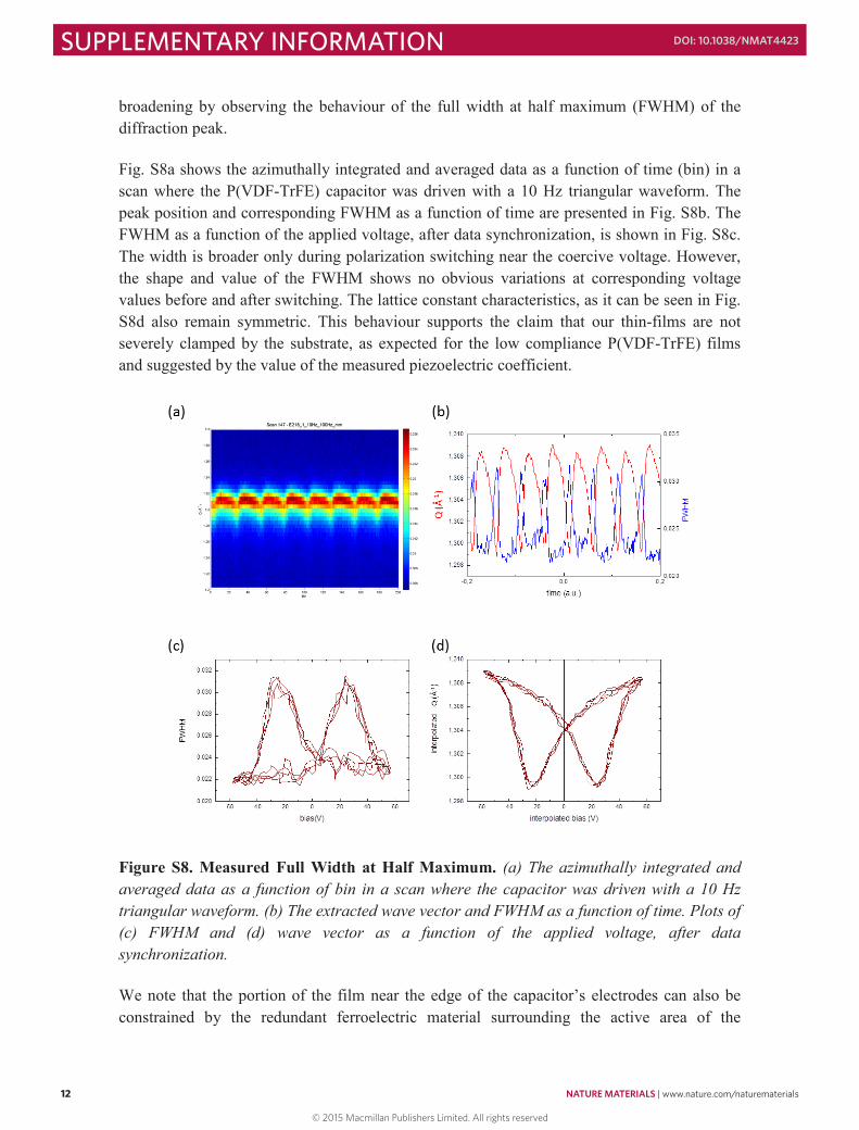
broadening by observing the behaviour of the full width at half maximum (FWHM) of the diffraction peak.
Fig. S8a shows the azimuthally integrated and averaged data as a function of time (bin) in a scan where the P(VDF-TrFE) capacitor was driven with a 10 Hz triangular waveform. The peak position and corresponding FWHM as a function of time are presented in Fig. S8b. The FWHM as a function of the applied voltage, after data synchronization, is shown in Fig. S8c.The width is broader only during polarization switching near the coercive voltage. However, the shape and value of the FWHM shows no obvious variations at corresponding voltage values before and after switching. The lattice constant characteristics, as it can be seen in Fig. S8d also remain symmetric. This behaviour supports the claim that our thin-films are not severely clamped by the substrate, as expected for the low compliance P(VDF-TrFE) films and suggested by the value of the measured piezoelectric coefficient.
Figure S8. Measured Full Width at Half Maximum. (a) The azimuthally integrated and averaged data as a function of bin in a scan where the capacitor was driven with a 10 Hz triangular waveform. (b) The extracted wave vector and FWHM as a function of time. Plots of (c) FWHM and (d) wave vector as a function of the applied voltage, after data synchronization.
We note that the portion of the film near the edge of the capacitor’s electrodes can also be constrained by the redundant ferroelectric material surrounding the active area of the
12
© 2015 Macmillan Publishers Limited. All rights reserved
NATURE MATERIALS | www.nature.com/naturematerials 13
SUPPLEMENTARY INFORMATIONDOI: 10.1038/NMAT4423
capacitor, as previously observed in inorganic ferroelectric capacitors.[12] P(VDF-TrFE), however, has a much lower elastic compliance (2GPa) as compared to PZT (120GPa).[13]
Nevertheless, to avoid any potential constrain effects from the redundant P(VDF-TrFE), the X-ray beam was always focused near the center of the capacitor.
9. Parameter extraction
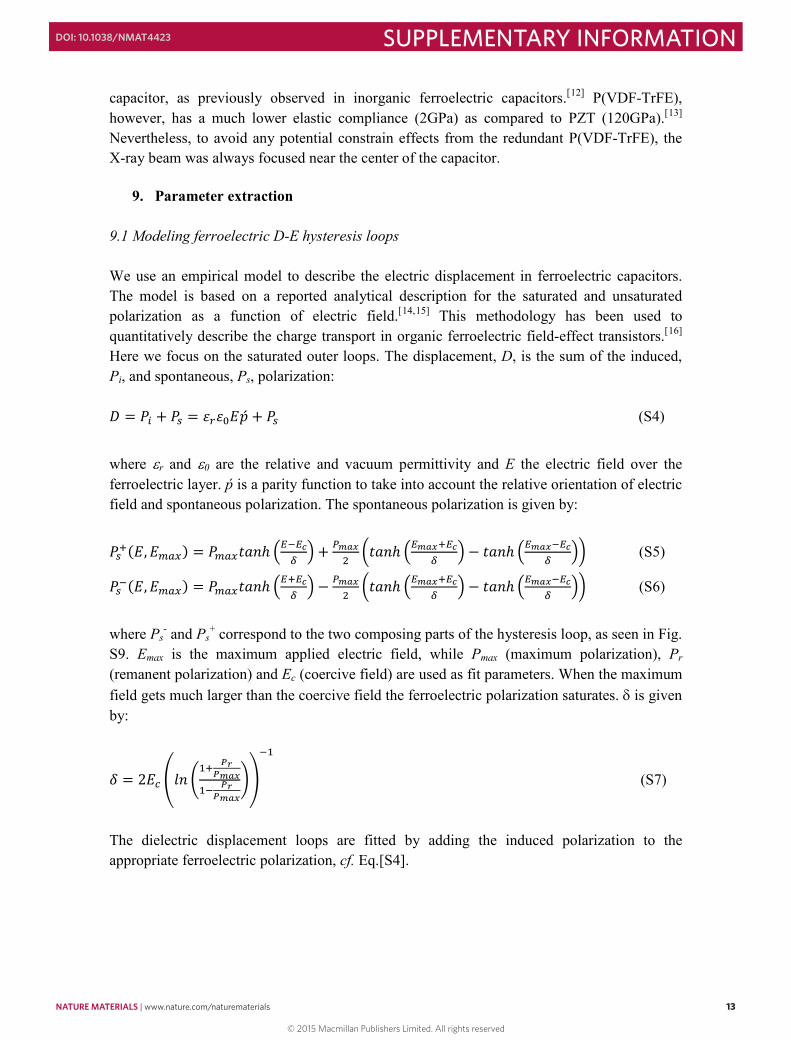
9.1 Modeling ferroelectric D-E hysteresis loops
We use an empirical model to describe the electric displacement in ferroelectric capacitors. The model is based on a reported analytical description for the saturated and unsaturated polarization as a function of electric field.[14,15] This methodology has been used to quantitatively describe the charge transport in organic ferroelectric field-effect transistors.[16]
Here we focus on the saturated outer loops. The displacement, D, is the sum of the induced,Pi, and spontaneous, Ps, polarization:
𝐷𝐷𝐷𝐷 = 𝑃𝑃𝑃𝑃𝑖𝑖𝑖𝑖 + 𝑃𝑃𝑃𝑃𝑠𝑠𝑠𝑠 = 𝜀𝜀𝜀𝜀𝑟𝑟𝑟𝑟𝜀𝜀𝜀𝜀0𝐸𝐸𝐸𝐸�́�𝑝𝑝𝑝 + 𝑃𝑃𝑃𝑃𝑠𝑠𝑠𝑠 (S4)
where εr and ε0 are the relative and vacuum permittivity and E the electric field over the ferroelectric layer. ṕ is a parity function to take into account the relative orientation of electric field and spontaneous polarization. The spontaneous polarization is given by:
𝑃𝑃𝑃𝑃𝑠𝑠𝑠𝑠+(𝐸𝐸𝐸𝐸,𝐸𝐸𝐸𝐸𝑚𝑚𝑚𝑚𝑚𝑚𝑚𝑚𝑚𝑚𝑚𝑚) = 𝑃𝑃𝑃𝑃𝑚𝑚𝑚𝑚𝑚𝑚𝑚𝑚𝑚𝑚𝑚𝑚𝑡𝑡𝑡𝑡𝑡𝑡𝑡𝑡𝑡𝑡𝑡𝑡ℎ �𝐸𝐸𝐸𝐸−𝐸𝐸𝐸𝐸𝑐𝑐𝑐𝑐𝛿𝛿𝛿𝛿� + 𝜕𝜕𝜕𝜕𝑚𝑚𝑚𝑚𝑚𝑚𝑚𝑚𝑚𝑚𝑚𝑚
2�𝑡𝑡𝑡𝑡𝑡𝑡𝑡𝑡𝑡𝑡𝑡𝑡ℎ �𝐸𝐸𝐸𝐸𝑚𝑚𝑚𝑚𝑚𝑚𝑚𝑚𝑚𝑚𝑚𝑚+𝐸𝐸𝐸𝐸𝑐𝑐𝑐𝑐
𝛿𝛿𝛿𝛿� − 𝑡𝑡𝑡𝑡𝑡𝑡𝑡𝑡𝑡𝑡𝑡𝑡ℎ �𝐸𝐸𝐸𝐸𝑚𝑚𝑚𝑚𝑚𝑚𝑚𝑚𝑚𝑚𝑚𝑚−𝐸𝐸𝐸𝐸𝑐𝑐𝑐𝑐
𝛿𝛿𝛿𝛿�� (S5)
𝑃𝑃𝑃𝑃𝑠𝑠𝑠𝑠−(𝐸𝐸𝐸𝐸,𝐸𝐸𝐸𝐸𝑚𝑚𝑚𝑚𝑚𝑚𝑚𝑚𝑚𝑚𝑚𝑚) = 𝑃𝑃𝑃𝑃𝑚𝑚𝑚𝑚𝑚𝑚𝑚𝑚𝑚𝑚𝑚𝑚𝑡𝑡𝑡𝑡𝑡𝑡𝑡𝑡𝑡𝑡𝑡𝑡ℎ �𝐸𝐸𝐸𝐸+𝐸𝐸𝐸𝐸𝑐𝑐𝑐𝑐𝛿𝛿𝛿𝛿� − 𝜕𝜕𝜕𝜕𝑚𝑚𝑚𝑚𝑚𝑚𝑚𝑚𝑚𝑚𝑚𝑚
2�𝑡𝑡𝑡𝑡𝑡𝑡𝑡𝑡𝑡𝑡𝑡𝑡ℎ �𝐸𝐸𝐸𝐸𝑚𝑚𝑚𝑚𝑚𝑚𝑚𝑚𝑚𝑚𝑚𝑚+𝐸𝐸𝐸𝐸𝑐𝑐𝑐𝑐
𝛿𝛿𝛿𝛿� − 𝑡𝑡𝑡𝑡𝑡𝑡𝑡𝑡𝑡𝑡𝑡𝑡ℎ �𝐸𝐸𝐸𝐸𝑚𝑚𝑚𝑚𝑚𝑚𝑚𝑚𝑚𝑚𝑚𝑚−𝐸𝐸𝐸𝐸𝑐𝑐𝑐𝑐
𝛿𝛿𝛿𝛿�� (S6)
where Ps- and Ps
+ correspond to the two composing parts of the hysteresis loop, as seen in Fig. S9. Emax is the maximum applied electric field, while Pmax (maximum polarization), Pr
(remanent polarization) and Ec (coercive field) are used as fit parameters. When the maximum field gets much larger than the coercive field the ferroelectric polarization saturates. δ is given by:
𝛿𝛿𝛿𝛿 = 2𝐸𝐸𝐸𝐸𝑐𝑐𝑐𝑐 �𝑙𝑙𝑙𝑙𝑡𝑡𝑡𝑡 �1+ 𝑃𝑃𝑃𝑃𝑟𝑟𝑟𝑟
𝑃𝑃𝑃𝑃𝑚𝑚𝑚𝑚𝑚𝑚𝑚𝑚𝑚𝑚𝑚𝑚
1− 𝑃𝑃𝑃𝑃𝑟𝑟𝑟𝑟𝑃𝑃𝑃𝑃𝑚𝑚𝑚𝑚𝑚𝑚𝑚𝑚𝑚𝑚𝑚𝑚
��
−1
(S7)
The dielectric displacement loops are fitted by adding the induced polarization to the appropriate ferroelectric polarization, cf. Eq.[S4].
13
© 2015 Macmillan Publishers Limited. All rights reserved
14 NATURE MATERIALS | www.nature.com/naturematerials
SUPPLEMENTARY INFORMATION DOI: 10.1038/NMAT4423
Figure S9. Modeling the ferroelectric D-E hysteresis loop. The measured displacement versus applied electric field for a ferroelectric P(VDF-TrFE) capacitor is presented as the black points. The solid lines are fits to the experimental data according to Eq.[S4-S7].
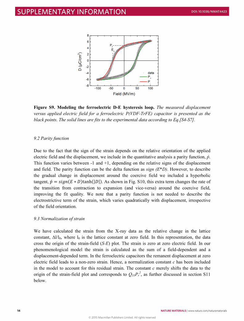
9.2 Parity function
Due to the fact that the sign of the strain depends on the relative orientation of the applied electric field and the displacement, we include in the quantitative analysis a parity function, ṕ.This function varies between -1 and +1, depending on the relative signs of the displacementand field. The parity function can be the delta function as sign (E*D). However, to describe the gradual change in displacement around the coercive field we included a hyperbolic tangent, �́�𝑝𝑝𝑝 = 𝑠𝑠𝑠𝑠𝑠𝑠𝑠𝑠𝑠𝑠𝑠𝑠𝑡𝑡𝑡𝑡(𝐸𝐸𝐸𝐸 ∗ 𝐷𝐷𝐷𝐷)tanh(|𝐷𝐷𝐷𝐷|). As shown in Fig. S10, this extra term changes the rate of the transition from contraction to expansion (and vice-versa) around the coercive field,improving the fit quality. We note that a parity function is not needed to describe the electrostrictive term of the strain, which varies quadratically with displacement, irrespective of the field orientation.
9.3 Normalization of strain
We have calculated the strain from the X-ray data as the relative change in the lattice constant, Δl/l0, where l0 is the lattice constant at zero field. In this representation, the data cross the origin of the strain-field (S-E) plot. The strain is zero at zero electric field. In our phenomenological model the strain is calculated as the sum of a field-dependent and a displacement-depended term. In the ferroelectric capacitors the remanent displacement at zero electric field leads to a non-zero strain. Hence, a normalization constant c has been included in the model to account for this residual strain. The constant c merely shifts the data to the origin of the strain-field plot and corresponds to Q33Pr
2, as further discussed in section S11 below.
14
© 2015 Macmillan Publishers Limited. All rights reserved
NATURE MATERIALS | www.nature.com/naturematerials 15
SUPPLEMENTARY INFORMATIONDOI: 10.1038/NMAT4423
Figure S10. Parity function. Example of (a) square and (b) gradual parity function for a P(VDF-TrFE) capacitor, with the corresponding fits of the S-E characteristics shown. The insets show the fits for the S-D representation of the data.
10. Data series of P(VDF-TrFE)
We measured the out-of-plane lattice constant and electric displacement while driving the capacitor with a triangular waveform. The frequency and amplitude of the driving signal were varied systematically. The full datasets and fits, as well as the extracted parameters, are presented in the following sections.
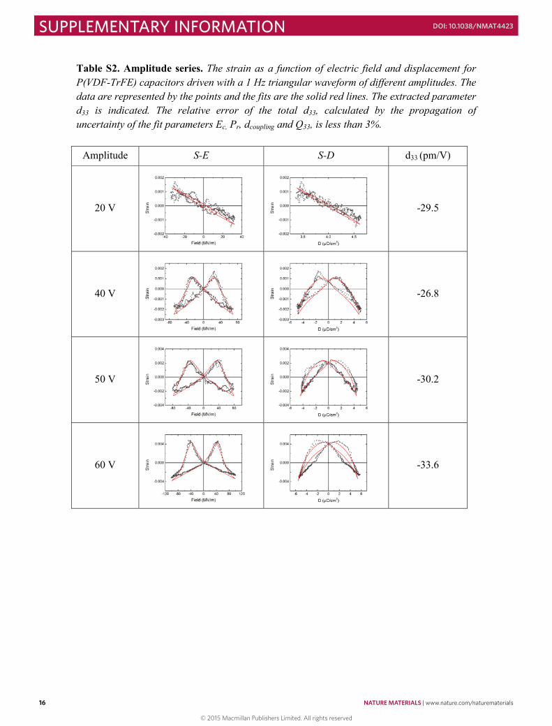
10.1 Amplitude series
The capacitors were driven with a triangular waveform with a frequency of 1 Hz. The amplitude was varied between 20 V and 60 V. The detector frequency was set at 50 Hz. Table S2 shows the strain as a function of electric field and displacement for different amplitudes. The data are represented by the points and the fits are the solid red lines. The extracted parameter d33 is indicated.
10.2 Frequency series
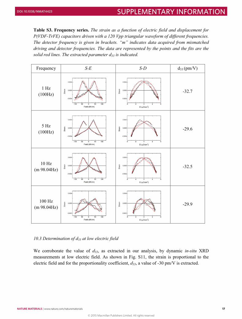
The capacitors were driven with a triangular waveform with an amplitude of 60 V. The frequency was varied between 1 Hz and 100 Hz. Table S3 shows the strain as a function of electric field and displacement for different frequency of the driving signal. The detector frequency is indicated. An “m” indicates data acquired from mismatched driving and detector frequencies. The data are represented by the points and the fits are the solid red lines. The extracted parameter d33 is indicated.
15
© 2015 Macmillan Publishers Limited. All rights reserved
16 NATURE MATERIALS | www.nature.com/naturematerials
SUPPLEMENTARY INFORMATION DOI: 10.1038/NMAT4423
Table S2. Amplitude series. The strain as a function of electric field and displacement for P(VDF-TrFE) capacitors driven with a 1 Hz triangular waveform of different amplitudes. The data are represented by the points and the fits are the solid red lines. The extracted parameter d33 is indicated. The relative error of the total d33, calculated by the propagation of uncertainty of the fit parameters Ec, Pr, dcoupling and Q33, is less than 3%.
Amplitude S-E S-D d33 (pm/V)
20 V -29.5
40 V -26.8
50 V -30.2
60 V -33.6
16
© 2015 Macmillan Publishers Limited. All rights reserved
NATURE MATERIALS | www.nature.com/naturematerials 17
SUPPLEMENTARY INFORMATIONDOI: 10.1038/NMAT4423
Table S3. Frequency series. The strain as a function of electric field and displacement for P(VDF-TrFE) capacitors driven with a 120 Vpp triangular waveform of different frequencies.The detector frequency is given in brackets. “m” indicates data acquired from mismatched driving and detector frequencies. The data are represented by the points and the fits are the solid red lines. The extracted parameter d33 is indicated.
Frequency S-E S-D d33 (pm/V)
1 Hz(100Hz)
-32.7
5 Hz(100Hz)
-29.6
10 Hz(m 98.04Hz)
-32.5
100 Hz(m 98.04Hz)
-29.9
10.3 Determination of d33 at low electric field
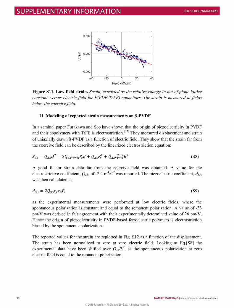
We corroborate the value of d33, as extracted in our analysis, by dynamic in-situ XRD measurements at low electric field. As shown in Fig. S11, the strain is proportional to the electric field and for the proportionality coefficient, d33, a value of -30 pm/V is extracted.
17
© 2015 Macmillan Publishers Limited. All rights reserved
18 NATURE MATERIALS | www.nature.com/naturematerials
SUPPLEMENTARY INFORMATION DOI: 10.1038/NMAT4423
Figure S11. Low-field strain. Strain, extracted as the relative change in out-of-plane lattice constant, versus electric field for P(VDF-TrFE) capacitors. The strain is measured at fieldsbelow the coercive field.
11. Modeling of reported strain measurements on β-PVDF
In a seminal paper Furakawa and Seo have shown that the origin of piezoelectricity in PVDF and their copolymers with TrFE is electrostriction.[17] They measured displacement and strain of uniaxially drawn β-PVDF as a function of electric field. They show that the strain far from the coercive field can be described by the linearized electrostriction equation:
𝑆𝑆𝑆𝑆33 = 𝑄𝑄𝑄𝑄33𝐷𝐷𝐷𝐷2 = 2𝑄𝑄𝑄𝑄33𝜀𝜀𝜀𝜀𝑟𝑟𝑟𝑟𝜀𝜀𝜀𝜀0𝑃𝑃𝑃𝑃𝑠𝑠𝑠𝑠𝐸𝐸𝐸𝐸 + 𝑄𝑄𝑄𝑄33𝑃𝑃𝑃𝑃𝑠𝑠𝑠𝑠2 + 𝑄𝑄𝑄𝑄33𝜀𝜀𝜀𝜀𝑟𝑟𝑟𝑟2𝜀𝜀𝜀𝜀02𝐸𝐸𝐸𝐸2 (S8)
A good fit for strain data far from the coercive field was obtained. A value for the electrostrictive coefficient, Q33, of -2.4 m4/C2 was reported. The piezoelectric coefficient, d33,was then calculated as:
𝑑𝑑𝑑𝑑33 = 2𝑄𝑄𝑄𝑄33𝜀𝜀𝜀𝜀𝑟𝑟𝑟𝑟𝜀𝜀𝜀𝜀0𝑃𝑃𝑃𝑃𝑟𝑟𝑟𝑟 (S9)
as the experimental measurements were performed at low electric fields, where the spontaneous polarization is constant and equal to the remanent polarization. A value of -33pm/V was derived in fair agreement with their experimentally determined value of 26 pm/V. Hence the origin of piezoelectricity in PVDF-based ferroelectric polymers is electrostrictionbiased by the spontaneous polarization.
The reported values for the strain are replotted in Fig. S12 as a function of the displacement. The strain has been normalized to zero at zero electric field. Looking at Eq.[S8] the experimental data have been shifted over Q33Pr
2, as the spontaneous polarization at zero electric field is equal to the remanent polarization.
18
© 2015 Macmillan Publishers Limited. All rights reserved
NATURE MATERIALS | www.nature.com/naturematerials 19
SUPPLEMENTARY INFORMATIONDOI: 10.1038/NMAT4423
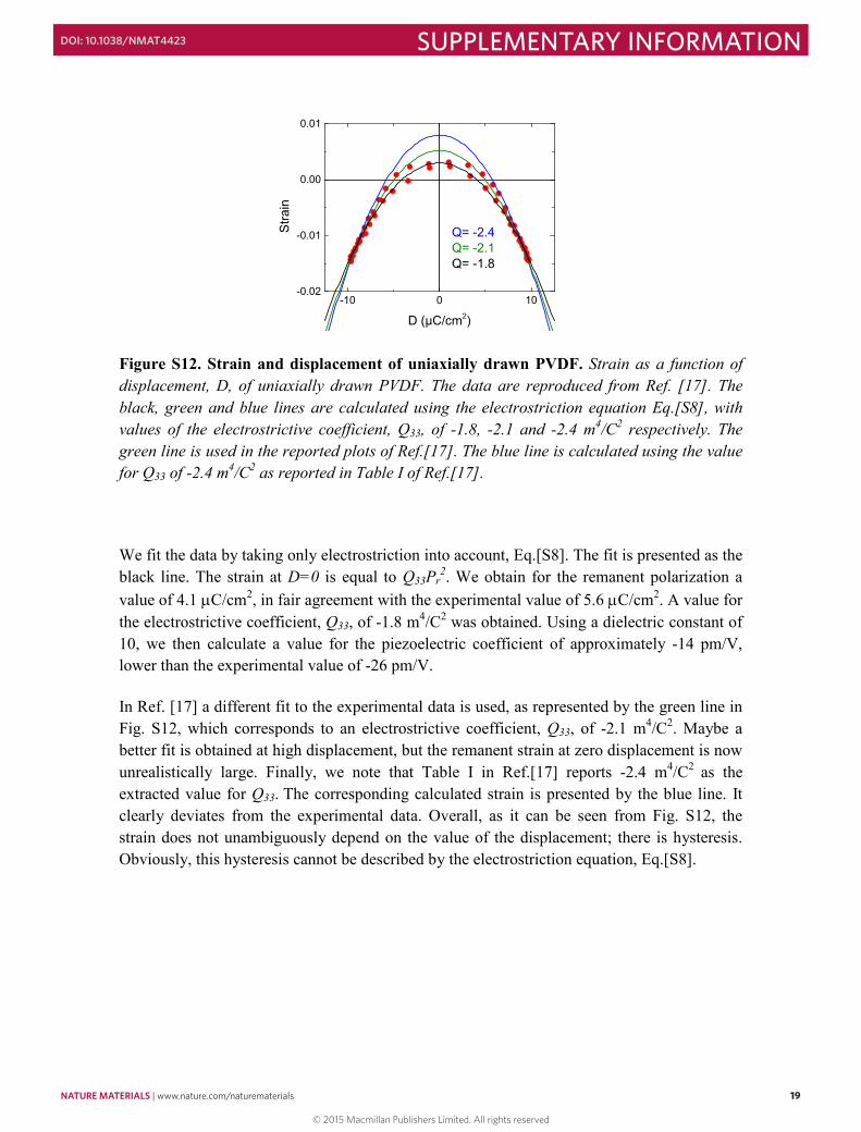
Figure S12. Strain and displacement of uniaxially drawn PVDF. Strain as a function of displacement, D, of uniaxially drawn PVDF. The data are reproduced from Ref. [17]. The black, green and blue lines are calculated using the electrostriction equation Eq.[S8], with values of the electrostrictive coefficient, Q33, of -1.8, -2.1 and -2.4 m4/C2 respectively. The green line is used in the reported plots of Ref.[17]. The blue line is calculated using the value for Q33 of -2.4 m4/C2 as reported in Table I of Ref.[17].
We fit the data by taking only electrostriction into account, Eq.[S8]. The fit is presented as the black line. The strain at D=0 is equal to Q33Pr
2. We obtain for the remanent polarization a value of 4.1 µC/cm2, in fair agreement with the experimental value of 5.6 µC/cm2. A value for the electrostrictive coefficient, Q33, of -1.8 m4/C2 was obtained. Using a dielectric constant of 10, we then calculate a value for the piezoelectric coefficient of approximately -14 pm/V,lower than the experimental value of -26 pm/V.
In Ref. [17] a different fit to the experimental data is used, as represented by the green line in Fig. S12, which corresponds to an electrostrictive coefficient, Q33, of -2.1 m4/C2. Maybe a better fit is obtained at high displacement, but the remanent strain at zero displacement is now unrealistically large. Finally, we note that Table I in Ref.[17] reports -2.4 m4/C2 as the extracted value for Q33. The corresponding calculated strain is presented by the blue line. It clearly deviates from the experimental data. Overall, as it can be seen from Fig. S12, the strain does not unambiguously depend on the value of the displacement; there is hysteresis.Obviously, this hysteresis cannot be described by the electrostriction equation, Eq.[S8].
-10 0 10-0.02
-0.01
0.00
0.01
Q= -2.4Q= -2.1Q= -1.8
Stra
in
D (μC/cm2)
19
© 2015 Macmillan Publishers Limited. All rights reserved
20 NATURE MATERIALS | www.nature.com/naturematerials
SUPPLEMENTARY INFORMATION DOI: 10.1038/NMAT4423
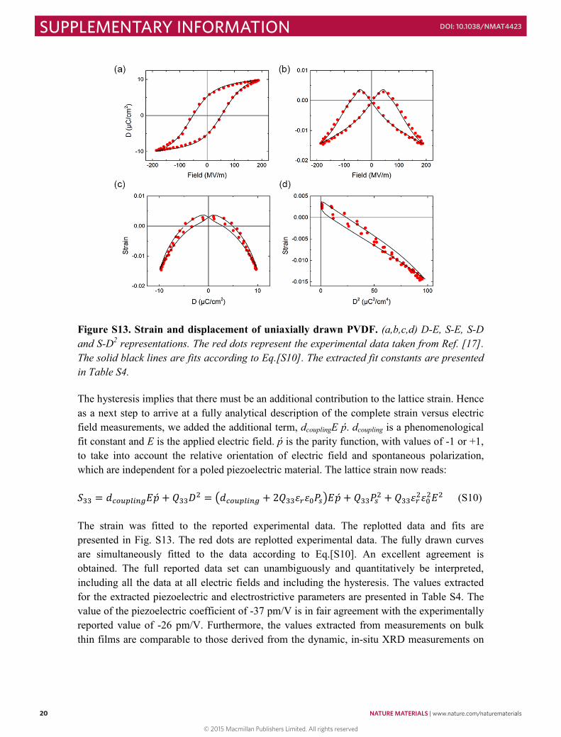
Figure S13. Strain and displacement of uniaxially drawn PVDF. (a,b,c,d) D-E, S-E, S-Dand S-D2 representations. The red dots represent the experimental data taken from Ref. [17]. The solid black lines are fits according to Eq.[S10]. The extracted fit constants are presented in Table S4.
The hysteresis implies that there must be an additional contribution to the lattice strain. Hence as a next step to arrive at a fully analytical description of the complete strain versus electricfield measurements, we added the additional term, dcouplingE ṕ. dcoupling is a phenomenological fit constant and E is the applied electric field. ṕ is the parity function, with values of -1 or +1, to take into account the relative orientation of electric field and spontaneous polarization, which are independent for a poled piezoelectric material. The lattice strain now reads:
𝑆𝑆𝑆𝑆33 = 𝑑𝑑𝑑𝑑𝑐𝑐𝑐𝑐𝑐𝑐𝑐𝑐𝑐𝑐𝑐𝑐𝑐𝑐𝑐𝑐𝜕𝜕𝜕𝜕𝜕𝜕𝜕𝜕𝜕𝜕𝜕𝜕𝑐𝑐𝑐𝑐𝐸𝐸𝐸𝐸�́�𝑝𝑝𝑝 + 𝑄𝑄𝑄𝑄33𝐷𝐷𝐷𝐷2 = �𝑑𝑑𝑑𝑑𝑐𝑐𝑐𝑐𝑐𝑐𝑐𝑐𝑐𝑐𝑐𝑐𝑐𝑐𝑐𝑐𝜕𝜕𝜕𝜕𝜕𝜕𝜕𝜕𝜕𝜕𝜕𝜕𝑐𝑐𝑐𝑐 + 2𝑄𝑄𝑄𝑄33𝜀𝜀𝜀𝜀𝑟𝑟𝑟𝑟𝜀𝜀𝜀𝜀0𝑃𝑃𝑃𝑃𝑠𝑠𝑠𝑠�𝐸𝐸𝐸𝐸�́�𝑝𝑝𝑝 + 𝑄𝑄𝑄𝑄33𝑃𝑃𝑃𝑃𝑠𝑠𝑠𝑠2 + 𝑄𝑄𝑄𝑄33𝜀𝜀𝜀𝜀𝑟𝑟𝑟𝑟2𝜀𝜀𝜀𝜀02𝐸𝐸𝐸𝐸2 (S10)
The strain was fitted to the reported experimental data. The replotted data and fits arepresented in Fig. S13. The red dots are replotted experimental data. The fully drawn curves are simultaneously fitted to the data according to Eq.[S10]. An excellent agreement is obtained. The full reported data set can unambiguously and quantitatively be interpreted, including all the data at all electric fields and including the hysteresis. The values extracted for the extracted piezoelectric and electrostrictive parameters are presented in Table S4. The value of the piezoelectric coefficient of -37 pm/V is in fair agreement with the experimentally reported value of -26 pm/V. Furthermore, the values extracted from measurements on bulk thin films are comparable to those derived from the dynamic, in-situ XRD measurements on
20
© 2015 Macmillan Publishers Limited. All rights reserved
NATURE MATERIALS | www.nature.com/naturematerials 21
SUPPLEMENTARY INFORMATIONDOI: 10.1038/NMAT4423
P(VDF-TrFE). The similar values once again indicate that piezoelectricity in PVDF and its copolymers is dominated by the change in the lattice constant.
Table S4. Extracted piezoelectric coefficients of uniaxially drawn PVDF
Material Ec(MV/m)
Pr(μC/cm2)
Q33(m4/C2)
dcoupling(pm/V)
2Qε0εrPr(pm/V)
d33(pm/V)
β-PVDF 58 5.5 -1.3 -25 -12.7 -37.7
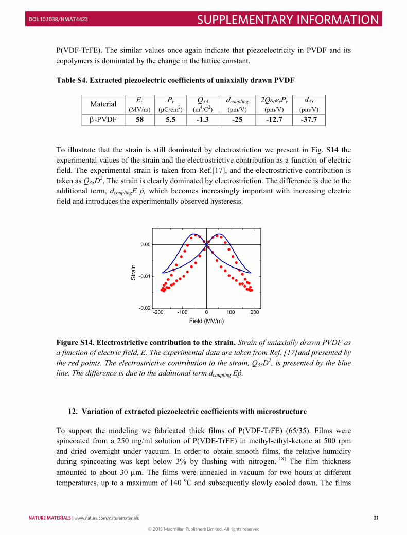
To illustrate that the strain is still dominated by electrostriction we present in Fig. S14 the experimental values of the strain and the electrostrictive contribution as a function of electric field. The experimental strain is taken from Ref.[17], and the electrostrictive contribution is taken as Q33D2. The strain is clearly dominated by electrostriction. The difference is due to the additional term, dcouplingE ṕ, which becomes increasingly important with increasing electric field and introduces the experimentally observed hysteresis.
Figure S14. Electrostrictive contribution to the strain. Strain of uniaxially drawn PVDF as a function of electric field, E. The experimental data are taken from Ref. [17]and presented by the red points. The electrostrictive contribution to the strain, Q33D2, is presented by the blue line. The difference is due to the additional term dcoupling Eṕ.
12. Variation of extracted piezoelectric coefficients with microstructure
To support the modeling we fabricated thick films of P(VDF-TrFE) (65/35). Films were spincoated from a 250 mg/ml solution of P(VDF-TrFE) in methyl-ethyl-ketone at 500 rpm and dried overnight under vacuum. In order to obtain smooth films, the relative humidity during spincoating was kept below 3% by flushing with nitrogen.[18] The film thickness amounted to about 30 µm. The films were annealed in vacuum for two hours at different temperatures, up to a maximum of 140 oC and subsequently slowly cooled down. The films
-200 -100 0 100 200-0.02
-0.01
0.00
Stra
in
Field (MV/m)
21
© 2015 Macmillan Publishers Limited. All rights reserved
22 NATURE MATERIALS | www.nature.com/naturematerials
SUPPLEMENTARY INFORMATION DOI: 10.1038/NMAT4423
annealed up to 100 oC could be easily peeled off the glass substrate by washing in deionized water with a little detergent. Films annealed at higher temperatures adhered to the substrates. To facilitate peeling off, the P(VDF-TrFE) films were spincoated on glass covered with an interlayer of PEDOT:PSS. The films were contacted on both sides with 100 nm thick circular evaporated gold contacts with an area of 0.78 cm2.
The films were characterized by differential scanning calorimetry measurements (DSC) and specular wide angle X-ray diffraction measurements (XRD), using a Philips PW1820 diffractometer with Cu radiation. DSC thermograms were recorded up on a Mettler-Toledo822/400 DSC with a modular measurement unit, using a heating rate of 10 K/min up to 200 oC. The displacement as a function of electric field was measured using a Radiant precision multiferroic test system (Radiant Technologies, Inc.). The strain as a function of electric field was measured simultaneously with the displacement, using a MTI 2100 photonic sensorinterfaced with the Radiant tester.
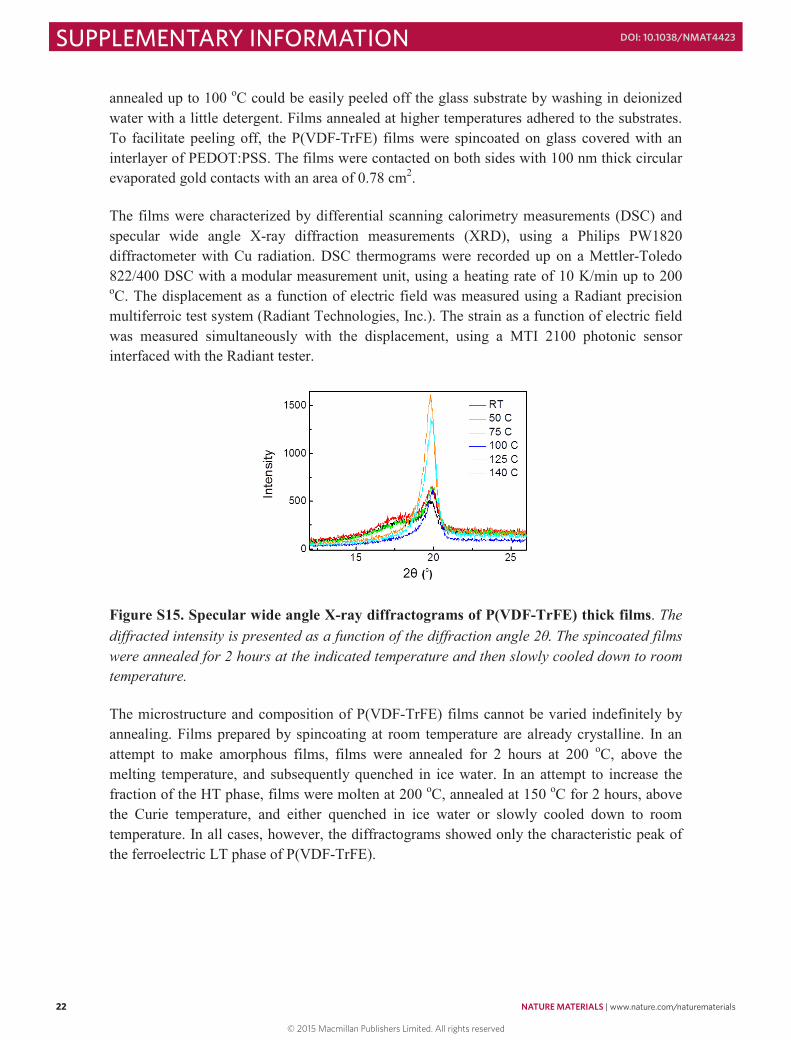
Figure S15. Specular wide angle X-ray diffractograms of P(VDF-TrFE) thick films. The diffracted intensity is presented as a function of the diffraction angle 2θ. The spincoated films were annealed for 2 hours at the indicated temperature and then slowly cooled down to room temperature.
The microstructure and composition of P(VDF-TrFE) films cannot be varied indefinitely by annealing. Films prepared by spincoating at room temperature are already crystalline. In an attempt to make amorphous films, films were annealed for 2 hours at 200 oC, above the melting temperature, and subsequently quenched in ice water. In an attempt to increase the fraction of the HT phase, films were molten at 200 oC, annealed at 150 oC for 2 hours, above the Curie temperature, and either quenched in ice water or slowly cooled down to room temperature. In all cases, however, the diffractograms showed only the characteristic peak of the ferroelectric LT phase of P(VDF-TrFE).
22
© 2015 Macmillan Publishers Limited. All rights reserved
NATURE MATERIALS | www.nature.com/naturematerials 23
SUPPLEMENTARY INFORMATIONDOI: 10.1038/NMAT4423
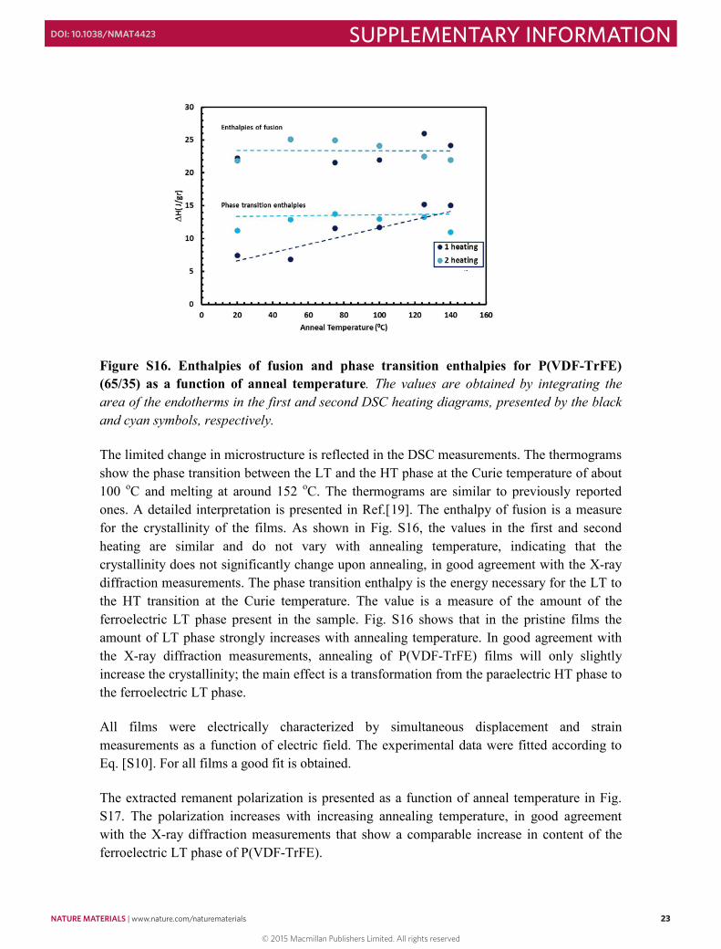
Figure S16. Enthalpies of fusion and phase transition enthalpies for P(VDF-TrFE) (65/35) as a function of anneal temperature. The values are obtained by integrating the area of the endotherms in the first and second DSC heating diagrams, presented by the black and cyan symbols, respectively.
The limited change in microstructure is reflected in the DSC measurements. The thermograms show the phase transition between the LT and the HT phase at the Curie temperature of about 100 oC and melting at around 152 oC. The thermograms are similar to previously reported ones. A detailed interpretation is presented in Ref.[19]. The enthalpy of fusion is a measure for the crystallinity of the films. As shown in Fig. S16, the values in the first and second heating are similar and do not vary with annealing temperature, indicating that the crystallinity does not significantly change upon annealing, in good agreement with the X-ray diffraction measurements. The phase transition enthalpy is the energy necessary for the LT to the HT transition at the Curie temperature. The value is a measure of the amount of the ferroelectric LT phase present in the sample. Fig. S16 shows that in the pristine films the amount of LT phase strongly increases with annealing temperature. In good agreement with the X-ray diffraction measurements, annealing of P(VDF-TrFE) films will only slightly increase the crystallinity; the main effect is a transformation from the paraelectric HT phase to the ferroelectric LT phase.
All films were electrically characterized by simultaneous displacement and strain measurements as a function of electric field. The experimental data were fitted according to Eq. [S10]. For all films a good fit is obtained.
The extracted remanent polarization is presented as a function of anneal temperature in Fig. S17. The polarization increases with increasing annealing temperature, in good agreement with the X-ray diffraction measurements that show a comparable increase in content of the ferroelectric LT phase of P(VDF-TrFE).
23
© 2015 Macmillan Publishers Limited. All rights reserved
24 NATURE MATERIALS | www.nature.com/naturematerials
SUPPLEMENTARY INFORMATION DOI: 10.1038/NMAT4423
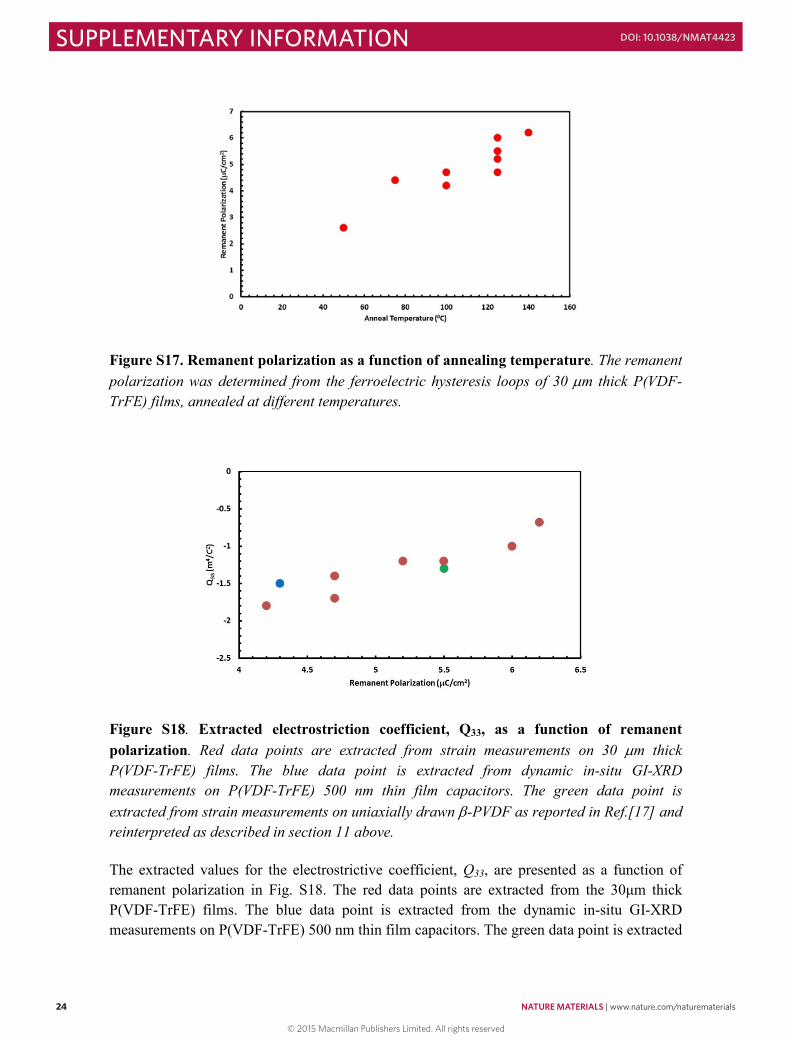
Figure S17. Remanent polarization as a function of annealing temperature. The remanent polarization was determined from the ferroelectric hysteresis loops of 30 µm thick P(VDF-TrFE) films, annealed at different temperatures.
Figure S18. Extracted electrostriction coefficient, Q33, as a function of remanent polarization. Red data points are extracted from strain measurements on 30 µm thick P(VDF-TrFE) films. The blue data point is extracted from dynamic in-situ GI-XRD measurements on P(VDF-TrFE) 500 nm thin film capacitors. The green data point is extracted from strain measurements on uniaxially drawn β-PVDF as reported in Ref.[17] andreinterpreted as described in section 11 above.
The extracted values for the electrostrictive coefficient, Q33, are presented as a function of remanent polarization in Fig. S18. The red data points are extracted from the 30μm thick P(VDF-TrFE) films. The blue data point is extracted from the dynamic in-situ GI-XRD measurements on P(VDF-TrFE) 500 nm thin film capacitors. The green data point is extracted
24
© 2015 Macmillan Publishers Limited. All rights reserved
NATURE MATERIALS | www.nature.com/naturematerials 25
SUPPLEMENTARY INFORMATIONDOI: 10.1038/NMAT4423
from strain measurements as reported in Ref.[17], and reinterpreted as described in section 11above, Table S4. The extracted values show a monotonous dependence on remanent polarization. We note that the electrostrictive coefficient is proportional to the compliance over the dielectric constant.[20] The Young’s modulus, which is the reciprocal of the compliance, has been reported for undrawn P(VDF-TrFE).[21] The films show so-called mechanical hardening as a result of poling; the Young’s modulus gradually increases with increasing remanent polarization.[21] Hence the change in the electrostriction coefficient with polarization can probably be explained by a change in Young’s modulus.
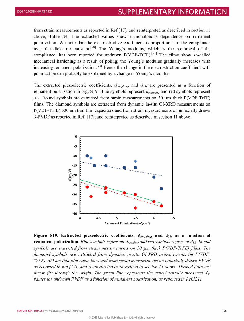
The extracted piezoelectric coefficients, dcoupling, and d33, are presented as a function of remanent polarization in Fig. S19. Blue symbols represent dcoupling and red symbols represent d33. Round symbols are extracted from strain measurements on 30 µm thick P(VDF-TrFE) films. The diamond symbols are extracted from dynamic in-situ GI-XRD measurements on P(VDF-TrFE) 500 nm thin film capacitors and from strain measurements on uniaxially drawn β-PVDF as reported in Ref. [17], and reinterpreted as described in section 11 above.
Figure S19. Extracted piezoelectric coefficients, dcoupling, and d33, as a function of remanent polarization. Blue symbols represent dcoupling and red symbols represent d33. Round symbols are extracted from strain measurements on 30 µm thick P(VDF-TrFE) films. The diamond symbols are extracted from dynamic in-situ GI-XRD measurements on P(VDF-TrFE) 500 nm thin film capacitors and from strain measurements on uniaxially drawn PVDF as reported in Ref.[17], and reinterpreted as described in section 11 above. Dashed lines are linear fits through the origin. The green line represents the experimentally measured d33
values for undrawn PVDF as a function of remanent polarization, as reported in Ref.[21].
25
© 2015 Macmillan Publishers Limited. All rights reserved
26 NATURE MATERIALS | www.nature.com/naturematerials
SUPPLEMENTARY INFORMATION DOI: 10.1038/NMAT4423
We have interpreted the piezoelectric coefficient, dcoupling, as being due to an additional electromechanical coupling between the intermixed crystalline lamellae and amorphous regions of the semi-crystalline polymer. The absolute value of dcoupling then should increase with the dipole density. Hence a relation with the remanent polarization might be expected. The blue dashed line is a linear fit to the data through the origin. In first order approximation, the experimental data can be well described.
The total longitudinal piezoelectric coefficient, d33, as measured at low electric fields, where the change in spontaneous polarization with electric field can be disregarded, is given by:
𝑑𝑑𝑑𝑑33 = 𝑑𝑑𝑑𝑑𝑆𝑆𝑆𝑆33𝑑𝑑𝑑𝑑(�́�𝑐𝑐𝑐𝐸𝐸𝐸𝐸)
�𝐸𝐸𝐸𝐸=0
= 𝑑𝑑𝑑𝑑𝑐𝑐𝑐𝑐𝑐𝑐𝑐𝑐𝑐𝑐𝑐𝑐𝑐𝑐𝑐𝑐𝜕𝜕𝜕𝜕𝜕𝜕𝜕𝜕𝜕𝜕𝜕𝜕𝑐𝑐𝑐𝑐 + 2𝑄𝑄𝑄𝑄33𝜀𝜀𝜀𝜀𝑟𝑟𝑟𝑟𝜀𝜀𝜀𝜀0𝑃𝑃𝑃𝑃𝑟𝑟𝑟𝑟 (S11)
When dcoupling depends linearly on the remanent polarization, then Eq.[S11] shows that the total extracted longitudinal piezoelectric coefficient, d33, should be directly proportional to the remanent polarization. We note that small deviations are expected due to the variation of the electrostrictive coefficient, Q33, with polarization as shown in Fig. S18. The red dashed line is a linear fit of the extracted d33 values as a function of remanent polarization. Within the experimentally limited range of remanent polarization an acceptable fit is obtained. More importantly, however, we present in Fig. S19 reported values of the longitudinal piezoelectric coefficient as a function of remanent polarization, as derived for undrawn PVDF.[21] Reported data are presented by the green line. An excellent agreement is obtained, supporting the analysis used.
Fig. S19 shows that the piezoelectric coefficient contains a contribution from electrostriction and from the additional electromechanical coupling between the intermixed crystalline lamellae and amorphous regions. For the films investigated both contributions are about equal in magnitude and scale with the remanent polarization. We note that the total strain remains dominated by electrostriction via the dominant contribution Q33Ps
2, as clearly shown in Fig. S14.
26
© 2015 Macmillan Publishers Limited. All rights reserved
NATURE MATERIALS | www.nature.com/naturematerials 27
SUPPLEMENTARY INFORMATIONDOI: 10.1038/NMAT4423
References
[1] Wada, Y. & Hayakawa, R. A model theory of piezo- and pyroelectricity of
poly(vinylidene fluoride) electret. Ferroelectrics 32, 115–118 (1981).
[2] Furukawa, T., When, J. X., Suzuki, K., Takashina, Y. & Date, M. Piezoelectricity and
pyroelectricity in vinylidene fluoride/trifluoroehtylene copolymers. J. Appl. Phys. 56,
829–834 (1984).
[3] Broadhurst, M. G. & Davis, G. T. Physical basis for piezoelectricity in PVDF.
Ferroelectrics, 60, 3–13 (1984).
[4] Greco, F. et al. Ultra-thin conductive free-standing PEDOT/PSS nanofilms. Soft Matter 7,10642-10650 (2011).
[5] Kepler, R. G. Ferroelectric Polymers, Ch. 3 in Ferroelectric Polymers: Chemistry:
Physics, and Applications, Edited Nalwa H.S. (Marcel Dekker, New York, 1995).
[6] Broadhurst, M. G., Davis, G. T., McKinney, J. E. & Collins, R. E. Piezoelectricity and
pyroelectricity in polyvinylidene fluoride–A model. J. Appl. Phys. 49, 4992–4997 (1978).
[7] Tashiro, K. Ferroelectric Polymers , Ch. 2, in Ferroelectric Polymers: Chemistry: Physics,
and Applications, Edited Nalwa H.S.(Marcel Dekker, New York, 1995).
[8] Lefki, K. & Dormans, J. M. Measurement of piezoelectric coefficients of ferroelectric thin
films. J. Appl. Phys. 76, 1764-1767 (1994).
[9] Lynch, S. Polyvinylidene fluoride (PVDF) elastic, piezoelectric, pyroelectric, and
dielectric coefficients and their nonlinearities. Ferroelectrics 150, 331-342 (1993).
[10] Bune, A. V. et al. Piezoelectric and pyroelectric properties of ferroelectric Langmuir-
Blodgett polymer films. J. App. Phys. 85, 7869-7873 (1999).
[11] Cheng, Z. et al. in Piezoelectric and Acoustic Materials for Transducer Applications (eds
Safari, A. et al.) Ch7, 141 (Springer, 2008).
[12] Nagarajan, V. et al. Dynamics of ferroelastic domains in ferroelectric thin films. Nat.
Mater. 2, 43-47 (2003).
[13] Xu, F., Chu, F. & Trolier-McKinstry, S. Longitudinal piezoelectric coefficient
measurement for bulk ceramics and thin films using pneumatic pressure rig. J. Appl. 27
© 2015 Macmillan Publishers Limited. All rights reserved
28 NATURE MATERIALS | www.nature.com/naturematerials
SUPPLEMENTARY INFORMATION DOI: 10.1038/NMAT4423
Phys. 86, 588-594 (1999).
[14] Miller, S. L. & McWhorter, P. J. Physics of the ferroelectric nonvolatile memory field
effect transistor. J. Appl. Phys. 72, 5999–6010 (1992).
[15] Lue, H.-T., Wu, C.-J. & Tseng, T.-Y. Device modeling of ferroelectric memory field-
effect transistor (FeMFET). IEEE T. Electron Dev. 49, 1790–1798 (2002).
[16] Brondijk, J. J., Asadi, K., Blom, P. W. M. & de Leeuw, D. M. Physics of organic
ferroelectric field-effect transistors. J. Polym. Sci. Pol. Phys. 50, 47–54 (2012).
[17] Furukawa, T. & Seo, N. Electrostriction as the origin of piezoelectricity in ferroelectric
polymers. Jpn. J. Appl. Phys. 29, 675–680 (1990).
[18] Li, M. et. al. Controlling the microstructure of poly(vinylidene-fluoride) (PVDF) thin
films for microelectronics, J. Mat. Chem. C 1, 7695-7702 (2013).
[19] Gregorio, R. Jr. & Botta, M. M. Effect of crystallization temperature on the phase
transitions of P(VDF/TrFE) copolymers, J. Polym. Sci. Pol. Phys. 36, 403-414 (1998).
[20] Newnham, R. E., Sundar, V., Yimnirun, R., Su, J. & Zhang, Q. M. Electrostriction:
nonlinear electromechanical coupling in solid dielectrics, J. Phys. Chem. B 101, 10141-
10150 (1997).
[21] Furakawa, T. Piezoelectricity and pyroelectricity in polymers, IEEE T. Electr. Insul. 24,
375-394 (1989).
28
© 2015 Macmillan Publishers Limited. All rights reserved