direct four-probe measurement of grain-boundary ... · direct four-probe measurement of...
TRANSCRIPT
Direct Four-Probe Measurement of Grain-Boundary Resistivity andMobility in Millimeter-Sized GrapheneRuisong Ma,†,‡ Qing Huan,† Liangmei Wu,†,‡ Jiahao Yan,†,‡ Wei Guo,§ Yu-Yang Zhang,† Shuai Wang,§
Lihong Bao,*,†,‡ Yunqi Liu,∥ Shixuan Du,†,‡ Sokrates T. Pantelides,⊥,† and Hong-Jun Gao*,†,‡
†Institute of Physics & University of Chinese Academy of Sciences, Chinese Academy of Sciences, P.O. Box 603, Beijing 100190,People’s Republic of China‡Beijing Key Laboratory for Nanomaterials and Nanodevices, Beijing 100190, People’s Republic of China§School of Chemistry and Chemical Engineering, Huazhong University of Science and Technology, Wuhan 430074, People’sRepublic of China∥Beijing National Laboratory for Molecular Sciences, Key Laboratory of Organic Solids, Institute of Chemistry, Chinese Academy ofScience, Beijing 100190, People’s Republic of China⊥Department of Physics and Astronomy and Department of Electrical Engineering and Computer Science, Vanderbilt University,Nashville, Tennessee 37235, United States
*S Supporting Information
ABSTRACT: Grain boundaries (GBs) in polycrystallinegraphene scatter charge carriers, which reduces carrier mobilityand limits graphene applications in high-speed electronics.Here we report the extraction of the resistivity of GBs and theeffect of GBs on carrier mobility by direct four-probemeasurements on millimeter-sized graphene bicrystals grownby chemical vapor deposition (CVD). To extract the GBresistivity and carrier mobility from direct four-probe intra-grain and intergrain measurements, an electronically equivalentextended 2D GB region is defined based on Ohm’s law.Measurements on seven representative GBs find that themaximum resistivities are in the range of several kΩ·μm tomore than 100 kΩ·μm. Furthermore, the mobility in thesedefective regions is reduced to 0.4−5.9‰ of the mobility of single-crystal, pristine graphene. Similarly, the effect of wrinkles oncarrier transport can also be derived. The present approach provides a reliable way to directly probe charge-carrier scattering atGBs and can be further applied to evaluate the GB effect of other two-dimensional polycrystalline materials, such as transition-metal dichalcogenides (TMDCs).
KEYWORDS: Graphene, grain boundary, wrinkle, four-probe measurement, mobility
Graphene’s extraordinary mechanical, optical, and electricalproperties1−3 make it an emerging material for a wide
range of applications, including field-effect transistors (FETs),4
flexible and transparent electrodes,5 and chemical/biochemicalsensors.6 However, an obstacle in practical electronicapplications of large-area graphene is its polycrystalline natureand the presence of defects such as grain boundaries (GBs) andwrinkles in as-synthesized graphene by chemical vapordeposition (CVD). As topological line defects, graphene GBsconsist of nonhexagonal carbon rings (pentagons, heptagons,and octagons), which have been imaged by scanning tunnelingmicroscopy (STM),7 scanning tunneling spectroscopy (STS),8
and high-resolution transmission electron microscopy(HRTEM).9,10 The electronic structure of pristine grapheneis strongly perturbed near GBs,11 whereby an “electronictransition width” ∼10 nm compared to the geometric width ofGB (<1 nm) has been revealed by STM/STS7,8,12,13 and
scanning tunneling potentiometry (STP).14 When chargecarriers transport through the GBs, they undergo strongscattering and the mobility is reduced.10,15−17 Therefore,quantitative characterization of charge-carrier transport acrosssuch topological defects by measuring their resistivity andcarrier mobility would facilitate large-scale technologicalapplications, such as touch-screen panels5,18 and solar-cellelectrodes.19−21
Previous investigations of electronic transport acrossgraphene GBs have been performed by conventional four-terminal measurements, in which the resistances of the pristinegrains on both sides and that of crossing the GB are measuredon Hall bar structures fabricated by microfabrication
Received: April 18, 2017Revised: July 13, 2017Published: August 8, 2017
Letter
pubs.acs.org/NanoLett
© XXXX American Chemical Society A DOI: 10.1021/acs.nanolett.7b01624Nano Lett. XXXX, XXX, XXX−XXX
technique.15,17 Taking the geometry factor into consideration,the intragrain resistivity and GB resistivity can bederived.6,15−17,22 Scanning probe microscope (SPM) related
techniques are also employed to investigate the transportproperties of GBs, such as STP,14 alternating currentelectrostatic force microscopy (AC-EFM)9 and Kelvin probeforce microscopy (KPFM).23 Direct four-probe measurementson millimeter-sized graphene without Hall bar devicefabrication have not yet been demonstrated.In this paper, we report direct four-probe measurements on
millimeter-sized graphene on a SiO2/Si substrate in a UHVfour-probe STM system.24 On the basis of Ohm’s law, the effectof a GB on transport can be effectively considered as theadditional resistance contribution from an extended 2D area.This extended area shares the same resistivity as the pristinegraphene grain and its extent can be represented by a parameterλ.17,22 By subtracting the intragrain contributions from theintergrain measurement, the parameter λ and GB resistivity canbe obtained. Furthermore, the mobility in the GB region canalso be derived. Our method is performed directly on thegraphene grains without preliminary lithographic fabricationand thus retains the original features and properties ofgraphene. It can also be further extended to measure the GBeffect in other 2D materials.Millimeter-sized graphene samples were grown on Cu foil
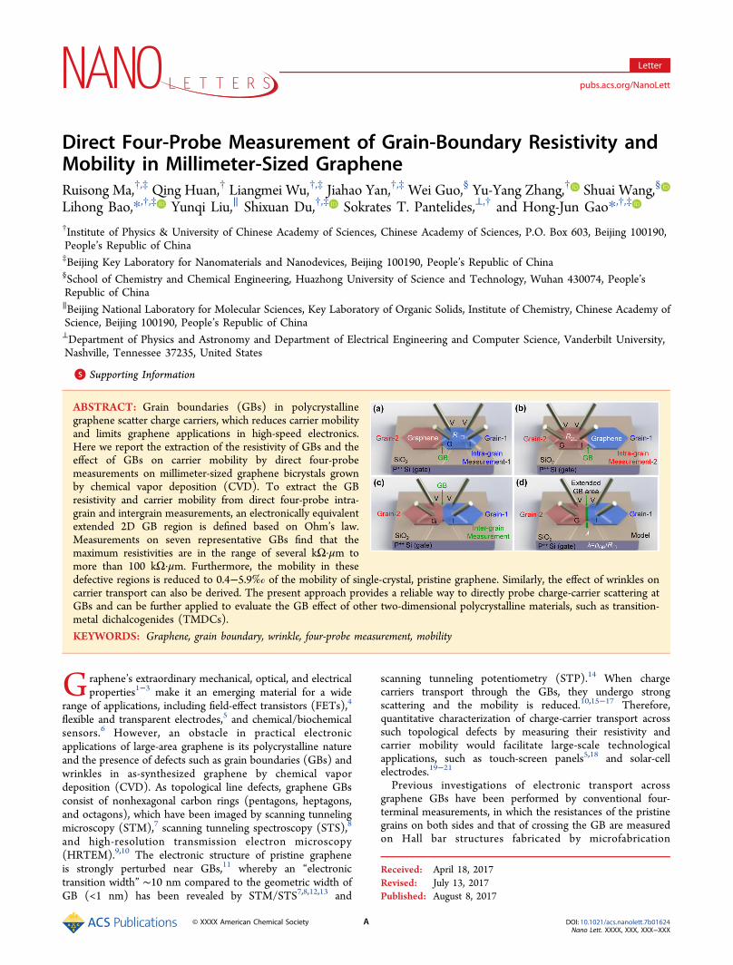
and then transferred onto a SiO2/Si wafer (see Methods sectionin Supporting Information).25 The graphene flakes can befound on Cu foil after CVD growth, as shown in the opticalmicrograph in Figure 1a. We see hexagonal islands that areidentified as single-crystal graphene. Direct TEM evidence hasbeen reported for similar samples in ref 10. Some of thehexagonal islands clearly form bicrystals. Nonhexagonal islands,on the other hand, are polycrystalline. We have carried outtransport measurements only on bicrystals, ensuring that wemeasure single GBs. STM characterization has been performedto verify the continuity and quality of graphene on Cu foil. Twotypical structures are shown in Figure 1b,c. Other morphologiesare shown in Supporting Information Figure S1. As can be seenfrom these STM images, the Cu foil has a highly corrugatedsurface consisting of many irregular steps and even small pits.Figure 1d clearly reveals moire patterns, formed by the latticemismatch of the graphene layer with the underlying Cu foilsurface. The uniform orientation of the moire pattern acrossneighboring terraces of copper confirms the continuity of thegraphene flake. The atomically resolved STM image of the
Figure 1. Optical and STM characterization of graphene grown on Cu foil by CVD. (a) Optical micrograph of graphene on a Cu foil substrate.Single-crystal, bicrystal and polycrystalline graphene flakes can be found on this micrograph. (b−c) Large-area STM image of graphene on Cu foil.The morphology of the Cu foil substrate is clearly resolved. (d) High-magnification STM image of the selected square region in (c). Hexagonalmoire pattern confirms the continuity of the graphene membrane on Cu substrate. (e) Atomically resolved STM image of the moire pattern. TheseSTM images verify the continuity and high quality of the graphene samples. Imaging parameters: (b) It = 250 pA and Vsample = 118.6 mV. (c) It =358.6 pA and Vsample = 87.16 mV. (d) It = 600 pA and Vsample = 87.16 mV. (e) It = 800 pA and Vsample = 87.16 mV.
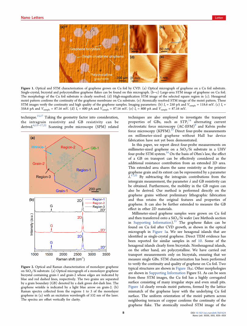
Figure 2. Optical and Raman characterization of monolayer grapheneon SiO2/Si substrate. (a) Optical micrograph of a monolayer graphenebicrystal containing grain-1 and grain-2 whose edges are indicated byblue and red dashed lines, respectively. The two grains are separatedby a grain boundary (GB) denoted by a dark green dot-dash line. Thegraphene wrinkle is indicated by a light blue arrow on grain-2. (b)Raman spectra collected from the regions 1 to 3 of the monolayergraphene in (a) with an excitation wavelength of 532 nm of the laser.The spectra are offset vertically for clarity.
Nano Letters Letter
DOI: 10.1021/acs.nanolett.7b01624Nano Lett. XXXX, XXX, XXX−XXX
B
moire pattern shown in Figure 1e further verifies the continuityand high quality of the CVD-grown graphene on Cu foil.Atomically resolved STM images on the structures shown inSupporting Information Figure S1 also confirm that defect-freegraphene is grown continuously as a single domain (SupportingInformation Figure S2).An optical micrograph of a transferred monolayer graphene
bicrystal onto SiO2/Si substrate is shown in Figure 2a in whichthe optical contrast verifies its monolayer nature.4,26 Thismillimeter-sized flake contains two coalesced graphene grains
whose edges are indicated by blue (grain-1) and red (grain-2)dashed lines, respectively. These two grains show nearly zerorotation angle, and the expected GB line can be revealed byconnecting the joint points of the two graphene domains on theedge,10 denoted by a dark green dot dash line in Figure 2a. Agraphene wrinkle on grain-2 is also indicated by a light bluearrow. Raman spectra of the graphene flake are collected atthree different regions (shown in Figure 2a) with an excitationwavelength of 532 nm of the laser, as presented in Figure 2b.The relative intensity ratio of the 2D and G peaks (>2:1)confirms the monolayer nature of this graphene bicrystal andthe absence of the D peak confirms the high quality of the flakeafter transferred onto the SiO2/Si substrate.
27
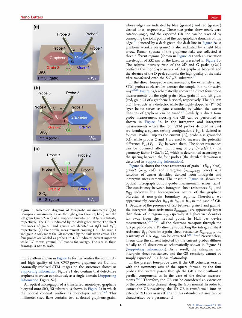
In the direct four-probe measurements, the extremely sharpSTM probes as electrodes contact the sample in a noninvasiveway.28,29 Figure 3a,b schematically shows the direct four-probemeasurements on the right grain (blue, grain-1) and left grain(red, grain-2) of a graphene bicrystal, respectively. The 300 nmSiO2 layer acts as a dielectric while the highly doped Si (P++ Si)layer below serves as gate electrode, by which the carrierdensities of graphene can be tuned.30 Similarly, a direct four-probe measurement crossing the GB can be performed asshown in Figure 3c. In the intragrain and intergrainmeasurements where the four STM probes denoted as 1−4are forming a square, testing configuration I1V23 is defined asfollows. Probe 1 injects the current (I1), probe 4 is grounded(G), while probes 2 and 3 are used to measure the potentialdifference V23 (V2 − V3) between them. The sheet resistancescan be obtained after multiplying RI1V23 (V23/I1) by thegeometry factor (∼2π/ln 2), which is determined according tothe spacing between the four probes (the detailed derivation isdescribed in Supporting Information).Figure 4a shows the sheet resistances of grain-1 (R1□, blue),
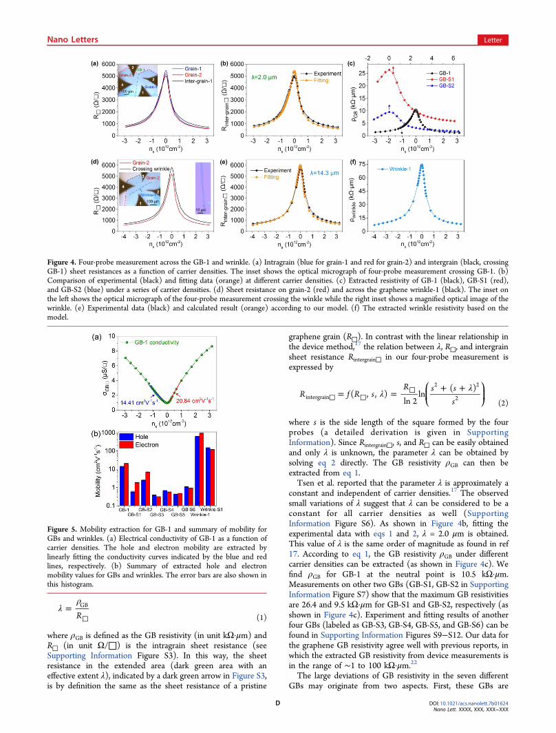
grain-2 (R2□, red), and intergrain (Rintergrain□, black) as afunction of carrier densities derived from intragrain andintergrain measurements. The inset in Figure 4a shows theoptical micrograph of four-probe measurement across GB-1.The consistency between intragrain sheet resistances R1□ andR2□ indicates the homogeneous nature of the graphenebicrystal at non-grain boundary regions. Therefore, weapproximately consider R1□ ≈ R2□ = R□ in the case of GB-1. Because of the presence of GB between grain-1 and grain-2,the intergrain sheet resistances Rintergrain□ are apparently largerthan those of intragrain R□, especially at high-carrier densitiesfar away from the neutral point. In Hall bar devicemeasurement,6,15−17,22 all the electrons transport through theGB perpendicularly. By directly subtracting the intragrain sheetresistance R□ from intergrain sheet resistance Rintergrain□, theresistivity of GB, ρGB, can be extracted.6,15−17,22 Nevertheless,in our case the current injected by the current probes diffusesradially to all directions as schematically shown in Figure S4(Supporting Information). As a result, the intragrain andintergrain sheet resistances, and the GB resistivity cannot besimply expressed in a linear relationship.In the present four-probe case, if the GB coincides exactly
with the symmetry axis of the square formed by the fourprobes, the current passes through the GB almost without aparallel component, as in the case of the device measure-ments.15,17 Therefore, the GB can be considered an extensionof the conductance channel along the GB’s normal. In order toextract the GB resistivity, the 1D GB is transformed into anextended 2D area as in ref 17 and this extended 2D area can becharacterized by a parameter λ
Figure 3. Schematic diagrams of four-probe measurements. (a,b)Four-probe measurements on the right grain (grain-1, blue) and theleft grain (grain-2, red) of a graphene bicrystal on SiO2/Si substrate,respectively. The GB is indicated by the dark green arrow. The sheetresistances of grain-1 and grain-2 are denoted as R1□ and R2□,respectively. (c) Four-probe measurement crossing GB. The grain-1and grain-2 coalesce at the GB indicated by the dark green arrow. Thefour probes are labeled as probe 1 to 4. “I” indicates current injectionwhile “G” means ground. “V” stands for voltage. The size in thesedrawings is not to scale.
Nano Letters Letter
DOI: 10.1021/acs.nanolett.7b01624Nano Lett. XXXX, XXX, XXX−XXX
C
λρ
=□R
GB
(1)
where ρGB is defined as the GB resistivity (in unit kΩ·μm) andR□ (in unit Ω/□) is the intragrain sheet resistance (seeSupporting Information Figure S3). In this way, the sheetresistance in the extended area (dark green area with aneffective extent λ), indicated by a dark green arrow in Figure S3,is by definition the same as the sheet resistance of a pristine
graphene grain (R□). In contrast with the linear relationship inthe device method,17 the relation between λ, R□, and intergrainsheet resistance Rintergrain□ in our four-probe measurement isexpressed by
λ λ= = + +□ □
□ ⎛⎝⎜
⎞⎠⎟R f R s
R s ss
( , , )ln 2
ln( )
intergrain
2 2
2(2)
where s is the side length of the square formed by the fourprobes (a detailed derivation is given in SupportingInformation). Since Rintergrain□, s, and R□ can be easily obtainedand only λ is unknown, the parameter λ can be obtained bysolving eq 2 directly. The GB resistivity ρGB can then beextracted from eq 1.Tsen et al. reported that the parameter λ is approximately a
constant and independent of carrier densities.17 The observedsmall variations of λ suggest that λ can be considered to be aconstant for all carrier densities as well (SupportingInformation Figure S6). As shown in Figure 4b, fitting theexperimental data with eqs 1 and 2, λ = 2.0 μm is obtained.This value of λ is the same order of magnitude as found in ref17. According to eq 1, the GB resistivity ρGB under differentcarrier densities can be extracted (as shown in Figure 4c). Wefind ρGB for GB-1 at the neutral point is 10.5 kΩ·μm.Measurements on other two GBs (GB-S1, GB-S2 in SupportingInformation Figure S7) show that the maximum GB resistivitiesare 26.4 and 9.5 kΩ·μm for GB-S1 and GB-S2, respectively (asshown in Figure 4c). Experiment and fitting results of anotherfour GBs (labeled as GB-S3, GB-S4, GB-S5, and GB-S6) can befound in Supporting Information Figures S9−S12. Our data forthe graphene GB resistivity agree well with previous reports, inwhich the extracted GB resistivity from device measurements isin the range of ∼1 to 100 kΩ·μm.22The large deviations of GB resistivity in the seven different
GBs may originate from two aspects. First, these GBs are
Figure 4. Four-probe measurement across the GB-1 and wrinkle. (a) Intragrain (blue for grain-1 and red for grain-2) and intergrain (black, crossingGB-1) sheet resistances as a function of carrier densities. The inset shows the optical micrograph of four-probe measurement crossing GB-1. (b)Comparison of experimental (black) and fitting data (orange) at different carrier densities. (c) Extracted resistivity of GB-1 (black), GB-S1 (red),and GB-S2 (blue) under a series of carrier densities. (d) Sheet resistance on grain-2 (red) and across the graphene wrinkle-1 (black). The inset onthe left shows the optical micrograph of the four-probe measurement crossing the winkle while the right inset shows a magnified optical image of thewrinkle. (e) Experimental data (black) and calculated result (orange) according to our model. (f) The extracted wrinkle resistivity based on themodel.
Figure 5. Mobility extraction for GB-1 and summary of mobility forGBs and wrinkles. (a) Electrical conductivity of GB-1 as a function ofcarrier densities. The hole and electron mobility are extracted bylinearly fitting the conductivity curves indicated by the blue and redlines, respectively. (b) Summary of extracted hole and electronmobility values for GBs and wrinkles. The error bars are also shown inthis histogram.
Nano Letters Letter
DOI: 10.1021/acs.nanolett.7b01624Nano Lett. XXXX, XXX, XXX−XXX
D
formed when pristine graphene domains are stitched togetherto generate a larger domain during growth and better intergrainconnectivity would lead to lower GB resistivity.17 Therefore,the difference in intergrain connectivity can result in thedeviations of GB resistivity. Second, the difference may comefrom functional groups or adsorbates, which preferentiallyattach to these defective GBs8 and can effectively change theGB resistivity.6,22 The difference in content and variety of theresidual attachment after vacuum annealing also gives rise tothe deviations of GB resistivity.The wrinkle resistivity can also be extracted through similar
measurements for GB, as shown in the inset of Figure 4d. Theintragrain (pristine, red) and intergrain (crossing wrinkle,black) sheet resistances as a function of carrier densities areshown in Figure 4d. The sheet resistance crossing wrinkle-1 isapparently larger than that of pristine graphene, indicating theadditional resistance contribution from a wrinkle when carrierstransport through it. Fitting the experimental data with eqs 1and 2, λ = 14.3 μm can be obtained. The wrinkle resistivity atneutral point is 74.5 kΩ·μm as shown in Figure 4f. By the samemethod, the effective parameter λ and maximum wrinkleresistivity of wrinkle-S1 are 17.9 μm and 146.2 kΩ·μm(Supporting Information Figure S13).The presence of GBs would alter the electronic structure
near the GB region over a scale ∼10 nm as verified by STM,STS, and STP.8,12−14 An STM image of a graphene GB on Cufoil is shown in Figure S15a (Supporting Information). Thewidth W of this GB is approximately 10 nm, as revealed by theline profile shown in Figure S10b (Supporting Information).According to previous STS studies, this electronic transitionregion, which is much wider in scale compared with theatomically sharp structural transition, arises from the dopingconcentration variation near the GB area.8,14 Because thescattering at the electronic transition region leads to theadditional resistance at GB, the mobility at the electronictransition region can be estimated from the GB resistivity.According to eq 1, the conductivity of the electronic transitionregion σGB□ can be calculated by
σρ
= =□□R
W1GB
GB GB (3)
in which RGB□ is the sheet resistance of the GB transitionregion whose width W is ∼10 nm.Accordingly, the conductivity of the electronic transition
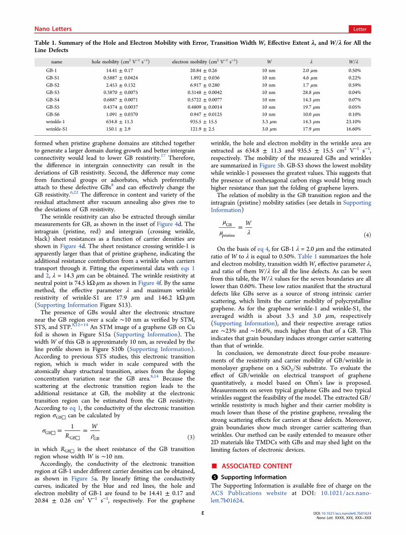
region at GB-1 under different carrier densities can be obtained,as shown in Figure 5a. By linearly fitting the conductivitycurves, indicated by the blue and red lines, the hole andelectron mobility of GB-1 are found to be 14.41 ± 0.17 and20.84 ± 0.26 cm2 V−1 s−1, respectively. For the graphene
wrinkle, the hole and electron mobility in the wrinkle area areextracted as 634.8 ± 11.3 and 935.5 ± 15.5 cm2 V−1 s−1,respectively. The mobility of the measured GBs and wrinklesare summarized in Figure 5b. GB-S3 shows the lowest mobilitywhile wrinkle-1 possesses the greatest values. This suggests thatthe presence of nonhexagonal carbon rings would bring muchhigher resistance than just the folding of graphene layers.The relation of mobility in the GB transition region and the
intragrain (pristine) mobility satisfies (see details in SupportingInformation)
μμ λ
= WGB
pristine (4)
On the basis of eq 4, for GB-1 λ = 2.0 μm and the estimatedratio of W to λ is equal to 0.50%. Table 1 summarizes the holeand electron mobility, transition widthW, effective parameter λ,and ratio of them W/λ for all the line defects. As can be seenfrom this table, the W/λ values for the seven boundaries are alllower than 0.60%. These low ratios manifest that the structuraldefects like GBs serve as a source of strong intrinsic carrierscattering, which limits the carrier mobility of polycrystallinegraphene. As for the graphene wrinkle-1 and wrinkle-S1, theaveraged width is about 3.3 and 3.0 μm, respectively(Supporting Information), and their respective average ratiosare ∼23% and ∼16.6%, much higher than that of a GB. Thisindicates that grain boundary induces stronger carrier scatteringthan that of wrinkle.In conclusion, we demonstrate direct four-probe measure-
ments of the resistivity and carrier mobility of GB/wrinkle inmonolayer graphene on a SiO2/Si substrate. To evaluate theeffect of GB/wrinkle on electrical transport of graphenequantitatively, a model based on Ohm’s law is proposed.Measurements on seven typical graphene GBs and two typicalwrinkles suggest the feasibility of the model. The extracted GB/wrinkle resistivity is much higher and their carrier mobility ismuch lower than those of the pristine graphene, revealing thestrong scattering effects for carriers at these defects. Moreover,grain boundaries show much stronger carrier scattering thanwrinkles. Our method can be easily extended to measure other2D materials like TMDCs with GBs and may shed light on thelimiting factors of electronic devices.
■ ASSOCIATED CONTENT
*S Supporting InformationThe Supporting Information is available free of charge on theACS Publications website at DOI: 10.1021/acs.nano-lett.7b01624.
Table 1. Summary of the Hole and Electron Mobility with Error, Transition Width W, Effective Extent λ, and W/λ for All theLine Defects
name hole mobility (cm2 V−1 s−1) electron mobility (cm2 V−1 s−1) W λ W/λ
GB-1 14.41 ± 0.17 20.84 ± 0.26 10 nm 2.0 μm 0.50%GB-S1 0.5887 ± 0.0424 1.892 ± 0.036 10 nm 4.6 μm 0.22%GB-S2 2.453 ± 0.132 6.917 ± 0.280 10 nm 1.7 μm 0.59%GB-S3 0.3870 ± 0.0075 0.3148 ± 0.0042 10 nm 28.8 μm 0.04%GB-S4 0.6887 ± 0.0071 0.5722 ± 0.0077 10 nm 14.3 μm 0.07%GB-S5 0.4374 ± 0.0037 0.4809 ± 0.0014 10 nm 19.7 μm 0.05%GB-S6 1.091 ± 0.0370 0.947 ± 0.0125 10 nm 10.0 μm 0.10%wrinkle-1 634.8 ± 11.3 935.5 ± 15.5 3.3 μm 14.3 μm 23.10%wrinkle-S1 150.1 ± 2.9 121.9 ± 2.5 3.0 μm 17.9 μm 16.60%
Nano Letters Letter
DOI: 10.1021/acs.nanolett.7b01624Nano Lett. XXXX, XXX, XXX−XXX
E
CVD growth method of graphene on Cu foil and transfertechnique, characterization method (Raman spectra,electrical transport measurement, STM and AFMimaging), extraction of intragrain and intergrain sheetresistance, extending the 1D GB defect into a 2Ddomain, derivation of the sheet resistance crossing theGB, converting the gate voltage to sheet carrier densitiesof graphene, extraction of hole and electron mobility fora 2D sample, ratio of mobility at GB electronic transitionregion with intragrain mobility, width of the graphenewrinkle (PDF)
■ AUTHOR INFORMATIONCorresponding Authors*E-mail: [email protected].*E-mail: [email protected].
ORCIDYu-Yang Zhang: 0000-0002-9548-0021Shuai Wang: 0000-0001-9328-0408Lihong Bao: 0000-0002-2942-892XShixuan Du: 0000-0001-9323-1307Hong-Jun Gao: 0000-0002-6766-0623NotesThe authors declare no competing financial interest.
■ ACKNOWLEDGMENTSThis work is supported by National “973” Projects of China(Grant 2013CBA01600), National Key R&D Program of China(Grant 2016YFA0202300), National Natural Science Founda-tion of China (Grants 61474141, 61674170, 61335006,61390501, 51325204, 51210003), the Chinese Academy ofSciences (CAS), the CAS Pioneer Hundred Talents Program,and Youth Innovation Promotion Association of CAS(20150005). Work at Vanderbilt University was supported byU.S. Department of Energy Grant DE-FG02-09ER46554 andby the McMinn Endowment. Y.Y.Z. and S.T.P. acknowledgeNational Center for Supercomputing Applications, which issupported by the DOE Office of Science under Contract No.DE-AC02-05CH11231, and the Extreme Science and Engineer-ing Discovery Environment (XSEDE) which is supported byNational Science Foundation Grant ACI-1053575.
■ REFERENCES(1) Lee, C.; Wei, X. D.; Kysar, J. W.; Hone, J. Science 2008, 321(5887), 385−388.(2) Morozov, S. V.; Novoselov, K. S.; Katsnelson, M. I.; Schedin, F.;Elias, D. C.; Jaszczak, J. A.; Geim, A. K. Phys. Rev. Lett. 2008, 100 (1),016602.(3) Bonaccorso, F.; Sun, Z.; Hasan, T.; Ferrari, A. C. Nat. Photonics2010, 4 (9), 611−622.(4) Novoselov, K. S.; Geim, A. K.; Morozov, S. V.; Jiang, D.; Zhang,Y.; Dubonos, S. V.; Grigorieva, I. V.; Firsov, A. A. Science 2004, 306(5696), 666−669.(5) Bae, S.; Kim, H.; Lee, Y.; Xu, X. F.; Park, J.-S.; Zheng, Y.;Balakrishnan, J.; Lei, T.; Kim, H. R.; Song, Y. I.; Kim, Y.-J.; Kim, K. S.;Ozyilmaz, B.; Ahn, J.-H.; Hong, B. H.; Iijima, S. Nat. Nanotechnol.2010, 5 (8), 574−578.(6) Yasaei, P.; Kumar, B.; Hantehzadeh, R.; Kayyalha, M.; Baskin, A.;Repnin, N.; Wang, C.; Klie, R. F.; Chen, Y. P.; Kral, P.; Salehi-Khojin,A. Nat. Commun. 2014, 5, 4911.(7) Lahiri, J.; Lin, Y.; Bozkurt, P.; Oleynik, I. I.; Batzill, M. Nat.Nanotechnol. 2010, 5 (5), 326−329.
(8) Tapaszto, L.; Nemes-Incze, P.; Dobrik, G.; Yoo, K. J.; Hwang, C.;Biro, L. P. Appl. Phys. Lett. 2012, 100 (5), 053114.(9) Huang, P. Y.; Ruiz-Vargas, C. S.; van der Zande, A. M.; Whitney,W. S.; Levendorf, M. P.; Kevek, J. W.; Garg, S.; Alden, J. S.; Hustedt,C. J.; Zhu, Y.; Park, J.; McEuen, P. L.; Muller, D. A. Nature 2011, 469(7330), 389−392.(10) Guo, W.; Wu, B.; Li, Y.; Wang, L.; Chen, J.; Chen, B.; Zhang, Z.;Peng, L.; Wang, S.; Liu, Y. ACS Nano 2015, 9 (6), 5792−5798.(11) Castro Neto, A. H.; Guinea, F.; Peres, N. M. R.; Novoselov, K.S.; Geim, A. K. Rev. Mod. Phys. 2009, 81 (1), 109−162.(12) Nemes-Incze, P.; Vancso, P.; Osvath, Z.; Mark, G. I.; Jin, X.;Kim, Y.-S.; Hwang, C.; Lambin, P.; Chapelier, C.; PeterBiro, L. Carbon2013, 64, 178−186.(13) Koepke, J. C.; Wood, J. D.; Estrada, D.; Ong, Z.-Y.; He, K. T.;Pop, E.; Lyding, J. W. ACS Nano 2013, 7 (1), 75−86.(14) Clark, K. W.; Zhang, X.-G.; Vlassiouk, I. V.; He, G. W.; Feenstra,R. M.; Li, A.-P. ACS Nano 2013, 7 (9), 7956−7966.(15) Yu, Q.; Jauregui, L. A.; Wu, W.; Colby, R.; Tian, J.; Su, Z.; Cao,H.; Liu, Z.; Pandey, D.; Wei, D.; Chung, T. F.; Peng, P.; Guisinger, N.P.; Stach, E. A.; Bao, J.; Pei, S.-S.; Chen, Y. P. Nat. Mater. 2011, 10 (6),443−449.(16) Jauregui, L. A.; Cao, H. L.; Wu, W.; Yu, Q. K.; Chen, Y. P. SolidState Commun. 2011, 151 (16), 1100−1104.(17) Tsen, A. W.; Brown, L.; Levendorf, M. P.; Ghahari, F.; Huang,P. Y.; Havener, R. W.; Ruiz-Vargas, C. S.; Muller, D. A.; Kim, P.; Park,J. Science 2012, 336 (6085), 1143−1146.(18) Ryu, J.; Kim, Y.; Won, D.; Kim, N.; Park, J. S.; Lee, E.-K.; Cho,D.; Cho, S.-P.; Kim, S. J.; Ryu, G. H.; Shin, H. A. S.; Lee, Z.; Hong, B.H.; Cho, S. ACS Nano 2014, 8 (1), 950−956.(19) Wang, X.; Zhi, L.; Mullen, K. Nano Lett. 2008, 8 (1), 323−327.(20) Ahmad, M.; An, H.; Kim, Y. S.; Lee, J. H.; Jung, J.; Chun, S.-H.;Seo, Y. Nanotechnology 2012, 23 (28), 285705.(21) Wu, J.; Becerril, H. A.; Bao, Z.; Liu, Z.; Chen, Y.; Peumans, P.Appl. Phys. Lett. 2008, 92 (26), 263302.(22) Cummings, A. W.; Duong, D. L.; Nguyen, V. L.; Van Tuan, D.;Kotakoski, J.; Barrios Vargas, J. E.; Lee, Y. H.; Roche, S. Adv. Mater.2014, 26 (30), 5079−5094.(23) Willke, P.; Mohle, C.; Sinterhauf, A.; Kotzott, T.; Yu, H. K.;Wodtke, A.; Wenderoth, M. Carbon 2016, 102, 470−476.(24) Ma, R.; Huan, Q.; Wu, L.; Yan, J.; Zou, Q.; Wang, A.; Bobisch,C. A.; Bao, L.; Gao, H.-J. Rev. Sci. Instrum. 2017, 88 (6), 063704.(25) Guo, W.; Jing, F.; Xiao, J.; Zhou, C.; Lin, Y.; Wang, S. Adv.Mater. 2016, 28 (16), 3152−3158.(26) Blake, P.; Hill, E. W.; Neto, A. H. C.; Novoselov, K. S.; Jiang, D.;Yang, R.; Booth, T. J.; Geim, A. K. Appl. Phys. Lett. 2007, 91 (6),063124.(27) Ferrari, A. C.; Meyer, J. C.; Scardaci, V.; Casiraghi, C.; Lazzeri,M.; Mauri, F.; Piscanec, S.; Jiang, D.; Novoselov, K. S.; Roth, S.; Geim,A. K. Phys. Rev. Lett. 2006, 97 (18), 187401.(28) Nakayama, T.; Kubo, O.; Shingaya, Y.; Higuchi, S.; Hasegawa,T.; Jiang, C.-S.; Okuda, T.; Kuwahara, Y.; Takami, K.; Aono, M. Adv.Mater. 2012, 24 (13), 1675−1692.(29) Lu, H. L.; Zhang, C. D.; Guo, H. M.; Gao, H. J.; Liu, M.; Liu, J.;Collins, G.; Chen, C. L. ACS Appl. Mater. Interfaces 2010, 2 (9),2496−2499.(30) Dorgan, V. E.; Bae, M.-H.; Pop, E. Appl. Phys. Lett. 2010, 97 (8),082112.
Nano Letters Letter
DOI: 10.1021/acs.nanolett.7b01624Nano Lett. XXXX, XXX, XXX−XXX
F