approaches to measure the resistivity of grain boundaries
TRANSCRIPT

HAL Id: hal-03247064https://hal.archives-ouvertes.fr/hal-03247064
Submitted on 2 Jun 2021
HAL is a multi-disciplinary open accessarchive for the deposit and dissemination of sci-entific research documents, whether they are pub-lished or not. The documents may come fromteaching and research institutions in France orabroad, or from public or private research centers.
L’archive ouverte pluridisciplinaire HAL, estdestinée au dépôt et à la diffusion de documentsscientifiques de niveau recherche, publiés ou non,émanant des établissements d’enseignement et derecherche français ou étrangers, des laboratoirespublics ou privés.
Approaches to Measure the Resistivity of GrainBoundaries in Metals with High Sensitivity and Spatial
Resolution: A Case Study Employing CuHanna Bishara, Matteo Ghidelli, Gerhard Dehm
To cite this version:Hanna Bishara, Matteo Ghidelli, Gerhard Dehm. Approaches to Measure the Resistivity of GrainBoundaries in Metals with High Sensitivity and Spatial Resolution: A Case Study Employing Cu. ACSApplied Electronic Materials, American Chemical Society, 2020, 2 (7), pp.2049-2056. �10.1021/ac-saelm.0c00311�. �hal-03247064�

1
Approaches to Measure Resistivity of Grain Boundaries in Metals with High Sensitivity
and Spatial Resolution: A Case Study Employing Cu
Hanna Bishara1,*, Matteo Ghidelli1,2,, Gerhard Dehm1
1 Max-Planck-Institut für Eisenforschung GmbH, 40237 Düsseldorf, Germany
2 Laboratoire des Sciences des Procédés et des Matériaux (LSPM), CNRS, Université
Sorbonne Paris Nord, 93430, Villetaneuse, France
* Corresponding author: [email protected]
Abstract
It is well known that grain boundaries (GBs) increase the electrical resistivity of metals due to their
enhanced electron scattering. The resistivity values of GBs are determined by their atomic structure,
therefore, assessing local resistivity of GBs is highly significant for understanding structure-property
relationships. So far, the local electrical characterization of an individual GB did not receive much
attention, mainly due to the limited accuracy of the applied techniques, which were not sensitive enough
to detect the subtle differences in electrical resistivity values of highly symmetric GBs. Here, we
introduce a detailed methodology to probe in situ or ex situ the local resistivity of individual GBs in Cu,
a metallic model system we choose due to its low resistance. Both bulk Cu samples and thin films are
investigated and different approaches to obtain reliable and accurate resistivity measurements are
described, involving the Van der Pauw technique for macroscopic measurements as well as two
different 4-point-probe techniques for local in-situ measurements performed inside a scanning electron
microscope. The in-situ contacts are realized with needles accurately positioned by piezo driven
micromanipulators. Resistivity results obtained on coincidence site lattice GBs (incoherent S3 and
asymmetric S5) are reported and discussed. In addition, the key experimental details as well as pitfalls
in the measurement of individual GB resistivity are addressed.

2
Keywords: Grain boundary ; interface ; electrical resistivity, thin films; Copper
(graphical abstract)
Introduction
Grain boundaries (GBs) are among the most significant defects influencing electrical properties of
metals [1-5]. Specifically, many studies reveal that GBs are the dominant electron scattering source in
metals, reporting a higher contribution to resistivity than surface scattering even for low dimensional
materials such as thin films and nanowires [3-8]. The acquisition of resistivity values for different GBs
is a key parameter for the emerging studies involving the atomic structures, phases and physical
properties of GBs [9-13]. However, only few studies focus on resistivity measurement of an individual
GB and interconnect it with the atomic structure of the interface [13-17]. Attempts to locally measure
GB resistivity were limited by sample geometry, microstructure and sensitivity of the corresponding
electrical measurement techniques. Hence, additional experimental developments are required to locally
sense the resistivity of individual GBs.
The atomic structure of a GB is determined by its crystallography, i.e. relative orientation between
neighbouring grains and the corresponding grain boundary plane, possible atomic translations at the
GB, chemical composition, and temperature [10, 12, 18]. Computational studies on particular GB types
confirm that their structure determines the resistivity values [19-21]. As a consequence, different types
of coincidence site lattice (CSL) GBs can be distinguished by their values of resistivity. Moreover,
theoretical and experimental studies show that segregation can either decrease or increase the GB
resistivity depending on the GB type and alloying (impurity) element [17, 19, 22].

3
The measurement of electrical resistivity of an individual GB in metals has been reported using
several approaches. One possibility consists of measuring a macroscopic resistivity of a polycrystalline
sample with a known number of GBs, and then normalizing it by number of grains using mathematical
models [1, 5, 23-25]. A second approach considers growth of bulk bicrystals and then performing a
measurement across a single GB [17]. Various electrical measurement methods were employed for
acquiring the electrical resistivity of GBs, e.g. Eddy currents [23], potentiometer method [1],
superconducting quantum interface device (SQUID) [17] and conducting atomic force microscopy [26].
However, most of these methods can be exploited only at cryogenic temperatures. In the case of thin
films, the most advanced technique for the direct measurement of GB resistivity is based on isolation
of GBs from the surrounding materials by creating trenches around them and then perform local
electrical measurements [4, 14-16, 27]. The lines are either fabricated by focused ion beam (FIB)
milling [14, 15], or by lithography fabrication processes employed in nano-/microelectronics [4, 6, 16].
On such structures a single GB can be probed by an electrical measurement setup consisting of 4
needles. The needles, which are attached to piezo stages enabling an accurate positioning, are designed
for in situ scanning electron microscopy (SEM) operation and precise resistivity measurements. So far,
only the resistivity of high angle random GB containing tilt and twist components could be measured,
while the resistivity of CSL and low angle GBs could not be resolved within the sensitivity limits of the
measurement methods [14, 15].
Here, we introduce a detailed methodology enabling highly sensitive and accurate local resistivity
measurement of individual GB in bulk Cu and thin films. The paper presents crystal growth and sample
preparation methods, details on the electrical measurement technique, as well as three different methods
for local measurements of a single GB. Cu is used as a model material system as it is heavily used in
micro- and nanoelectronic devices as conduction lines. We measure the resistivity values of S3 and S5
GBs employing different techniques and compare the results. The presented methodology is highly
relevant for the emerging studies on GB structures, segregation, phases and resulting functional
properties.

4
2. Experimental
2.1 Cu Bicrystal Growth and Cu Thin Film Deposition
In order to perform electrical measurements of an individual GB, careful crystal growth and sample
preparation processes are required. Specifically, the samples must facilitate electrical measurements in
a single crystal (i.e. selected region without GBs) and a bicrystal region (i.e. selected region separated
by a single GB) within the same sample. Here, we briefly describe the Cu bicrystal growth process, Cu
thin film deposition, and sample preparation method employed in this study.
Cu bulk bicrystal were grown by the conventional Bridgman method as described in detail in [9,
28] using two seed crystals of pre-selected orientations. In the present case, two [100] oriented seed
crystals were used, one seed crystal was tilted by 36.9° along the [100] axis with respect to the other
single crystal seed to form an asymmetric S5 tilt grain boundary in [9, 28]. To obtain a bulk bicrystal,
a container of polycrystalline high purity Cu is in contact with the two seed crystals and heated slightly
above the melting point. By slowly solidifying the melt zone, an asymmetric S5 [100] bicrystal forms.
The bulk bicrystal is cut with spark erosion into 5- mm-thick cylindrical slices with the S5 GB extending
from the top to bottom surface of the slices. The atomic structure of the GB has been recently studied
by advanced scanning transmission electron microscopy as reported in [9].
Cu thin films of high purity (99.999% pure Cu) were sputtered at room temperature on (0001)-
oriented α-Al2O3 substrates (c-plane, 2 inch sapphire wafers). Sputtering was carried out with a radio
frequency (RF) power supply at 250W, a background pressure of 0.66 Pa and 20 sccm Ar flow. The
deposition time to achieve a nominally 500 nm thick film was 45 min. Grain growth of the highly (111)
textured Cu grains was achieved through post-thermal annealing at 400 °C for 3 hours within the
sputtering chamber in order to limit contamination and oxidation. Surface morphology and cross section
are inspected with SEM (Zeiss -Gemini 500). Crystallographic orientation of thin film and GB planes
are identified using electron backscattered diffraction (EBSD) SEM analysis (Zeiss Auriga SEM,
EDAX EBSD detector, OIM software) at 12 kV. Subsequently, individual GBs can be selected based
on the SEM-EBSD results and isolated within thin lines as described in Section 2.3.1.

5
2.2. Electrical measurements
The contribution of an individual GB resistivity to the resistance of a pure metal is relatively low ( ~2%)
[24]. As a matter of fact, any current-induced heating, drift of a contact, or minor geometrical
differences in samples might create deviation in measured resistance values within the same order of
magnitude of the GB resistance. Therefore, the electrical measurement method must ensure that these
factors are not affecting the experiment. For these reasons, persistent electrical measurements and an
optimized modulation of electrical current is adapted for obtaining highly reliable data. The technique
is based on applying a series of few hundreds of direct current (dc) pulses and measuring the
corresponding voltage at each pulse. The same electrical measurement technique is used for all methods
presented within this paper.
The electrical current is applied using a current generator (Keithly 6221) with 5-10.10-3 s long
pulses. The deadtime between subsequent pulses is set to 20 time the pulse time duration to avoid
overlapping. A voltage measurement is conducted at the pulse half-time employing a nanovoltmeter
(Keithly 2182A). The height of the pulse varied between 0.05-50 mA, depending on the measurement
geometry. Parameters of the pulses significantly affect the accuracy of measurements. For instance,
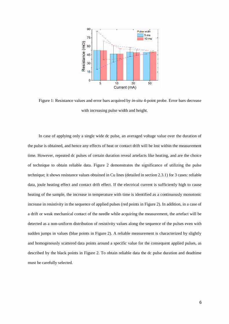
Figure 1 presents the electrical resistance values and error bars obtained for a Cu single crystal through
4-point-probe technique with 60 μm spacing between needles. Resistance values are given for 2 pulses
widths and 4 pulse heights. The data clearly show that increasing the pulse width from 5 ms to 10 ms
yields a decrease of 50-60% in standard deviation values of resistivity. Moreover, an increase of pulse
height from 5 mA to 50 mA shrinks the standard deviation by 11 times. Within such a geometry,
utilizing 50 mA pulses of 10 ms width gives a standard deviation of 2%. The accuracy is further
increased by repeating the experiment several times. In principle, higher currents yield a higher
accuracy in resistance values, but high currents can induce Joule heating of the sample or contacts.
6
Figure 1: Resistance values and error bars acquired by in-situ 4-point probe. Error bars decrease
with increasing pulse width and height.
In case of applying only a single wide dc pulse, an averaged voltage value over the duration of
the pulse is obtained, and hence any effects of heat or contact drift will be lost within the measurement
time. However, repeated dc pulses of certain duration reveal artefacts like heating, and are the choice
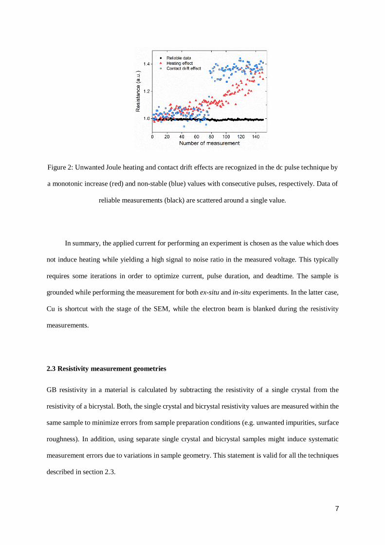
of technique to obtain reliable data. Figure 2 demonstrates the significance of utilizing the pulse
technique; it shows resistance values obtained in Cu lines (detailed in section 2.3.1) for 3 cases: reliable
data, joule heating effect and contact drift effect. If the electrical current is sufficiently high to cause
heating of the sample, the increase in temperature with time is identified as a continuously monotonic
increase in resistivity in the sequence of applied pulses (red points in Figure 2). In addition, in a case of
a drift or weak mechanical contact of the needle while acquiring the measurement, the artefact will be
detected as a non-uniform distribution of resistivity values along the sequence of the pulses even with
sudden jumps in values (blue points in Figure 2). A reliable measurement is characterized by slightly
and homogenously scattered data points around a specific value for the consequent applied pulses, as
described by the black points in Figure 2. To obtain reliable data the dc pulse duration and deadtime
must be carefully selected.
7
Figure 2: Unwanted Joule heating and contact drift effects are recognized in the dc pulse technique by
a monotonic increase (red) and non-stable (blue) values with consecutive pulses, respectively. Data of
reliable measurements (black) are scattered around a single value.
In summary, the applied current for performing an experiment is chosen as the value which does
not induce heating while yielding a high signal to noise ratio in the measured voltage. This typically
requires some iterations in order to optimize current, pulse duration, and deadtime. The sample is
grounded while performing the measurement for both ex-situ and in-situ experiments. In the latter case,
Cu is shortcut with the stage of the SEM, while the electron beam is blanked during the resistivity
measurements.
2.3 Resistivity measurement geometries
GB resistivity in a material is calculated by subtracting the resistivity of a single crystal from the
resistivity of a bicrystal. Both, the single crystal and bicrystal resistivity values are measured within the
same sample to minimize errors from sample preparation conditions (e.g. unwanted impurities, surface
roughness). In addition, using separate single crystal and bicrystal samples might induce systematic
measurement errors due to variations in sample geometry. This statement is valid for all the techniques
described in section 2.3.

8
2.3.1. Thin film samples
In order to locally characterize an individual GB, the specific boundary must be electrically and
physically isolated from any surrounding material. The geometry of measured features is chosen in a
way that it enables calculation of resistivity r [μΩ ∙ cm] from the measurement of the resistance R [Ω].
A convenient geometry is a line with length and cross section that contains GBs; the resistance R
of such a line is described by the analytical relation:
= + ∑ (1)
where the term ∑ in eq. (1) captures the contribution of GBs within the line of cross-section
AGB. Each GB possesses an individual resistivity [Ω ∙ ]. To simplify the analysis, the cross
section of the individual GB should be kept as identical as possible. Ideally, = . This means
that for an inclined GB the area > , and must be carefully determined. We discuss corrections
and tolerance in determining the in section 3. Also, effects like grain boundary grooving require
highly precise measurements to keep errors in at least one order of magnitude smaller than the
contribution of the GB to the measured resistance R compared to single crystal resistance.
In our study, a 400 °C annealing treatment for 3h leads to sufficiently large grain sizes (> 10µm). Then,
a line of typically more than 40 µm length was cut in the thin film by milling trenches on a pre-selected
area through the entire thickness of the film (Figure 3c). In our study a Ga FIB was employed and
milling done at a beam current of 50 pA. Figure 3 illustrates the described procedure. The ends of the
line remain connected to the surrounding film in order to avoid charging effects by the insulating
sapphire substrate during SEM imaging. Finally, local electrical properties are measured by probing the
line using piezo-controlled needles accurately positioned inside the SEM (Figure 3d). During the
resistivity measurements with the 4 probes, the electron beam of the SEM is blanked. Due to the absence
of grooving and invisibleness of GBs in secondary electron SEM imaging, the positions of GBs within
the lines are determined by projecting the grain map of EBSD measurement after the FIB milling on
the SEM image.

9
Figure 3: (a) Thin films are grown on (0001)-oriented α-Al2O3 substrates; (b) grain growth is obtained
by an annealing treatment. (c) GBs are separated from their surrounding region by FIB milling, the
line is still connected at its ends to the film. (d) Four micromanipulators are used to probe the bicrystal
electrical resistivity.
The length of the lines is 40-60 mm, and the width is around 600 nm. The width is elected based
on 2 considerations: (i) the width should exceed multiple times the mean free path of the electron in the
inspected material to minimize effects from surface scattering; the mean free path of electrons in Cu at
room temperature is 39 nm [29, 30]. (ii) The selected line width should support the mechanical contact
load of the electrode tips placed on the line, and keep drift of the electrode positions minimal.
Once the lines including the chosen GBs are prepared, the sample is inserted inside a SEM with
4 independent micromanipulators (Kleindiek Nanotechnik – PS4), each of them is equipped with a
Tungsten needle having a 50 nm curvature radius of the tip. The applied measurement geometry is
illustrated in Figure 4; it consists of two needles (needles 1 and 2) with fixed positions at the edges of
the line, which are used to apply a current. The other two needles, are used for voltage measurement,
one is fixed at constant position within the line (needle 3), and the other is a mobile one moving in steps
of ~1 mm towards the other voltage contact (needle 3) from position 4 towards 4’’’ (see Figure 4). A
series of resistivity measurements are conducted for different positions of needle 4. With this geometry,
any measured resistivity value corresponds to the material within the volume between the voltage
sensing needles 3 and 4 (Figure 4), including the resistivity of a known number of GBs. Thus, when the

10
mobile needle 4 moves and crosses an individual GB, a jump in resistance R is observed – this value
relates to the GB resistance.
Figure 4: Schematic of a line containing several GBs within the thin film. Positions of the 4 needles
used for the 4-point measurement technique are demonstrated. Needles 1-3 are fixed at specific
position during the experiment, while needle 4 moves along the line from position 4 to 4’’’. Several
GBs can be inspected within a single line.
2.3.2 Bulk samples using Van der Pauw method
The electrical resistivity measurement for bulk bicrystal has been carried out adapting the Van der Pauw
method [31, 32]. This technique is applied in the present case on the cylindrical bicrystal containing the
GB (see Figure 5a). For the resistivity measurement of the single crystal, all four needles must be
positioned on one side of the bicrystal, i.e. in a single crystal region (see Figure 5a, positions 1 to 4). In
that case needle 4 is located in the vicinity of the GB (Figure 5a). In order to measure subsequently the
resistivity of the bicrystal, needle 4 moves across the GB to position 4’, while needles 1 to 3 remain
fixed at their previous position (Figure 5a). This approach eliminates systematic errors as 3 needles stay
at the same position used for the single crystal resistivity measurement, while the fourth needle moves
only a short distance across the GB in a location close to its initial position as illustrated in Figure 5a
(see positions 4 and 4’). In order to confirm that the measured resistivity difference between single and
bicrystal corresponds to the presence of the GB rather than geometrical aspects, the resistivity
measurements are conducted 5 times repeatedly relocating the positions 4 and 4’ within the inspected
region. Each measurement is obtained within a distance x from the edge of sample, where the GB
intersects. Data presented in Figure 5b confirms the tolerance in positioning the needle. Changing the

11
position of only one needle by ≤ 0.5 mm affects the measured values by ≤ 0.6%. This deviation is
sufficiently small to measure an individual GB resistivity for Cu (see Figure 5b).
Figure 5: (a) Schematic of the Van der Pauw method; needle positions 1 to 4 are applied for the
resistivity measurements of a single grain of the bulk bicrystal, while positions 1 to 4’ sense the
bicrystal resistivity. Note that needles 1-3 are kept in the same position during the experiment, while
needle 4 is relocated to 4’. (b) Resistivity of the single and bicrystal obtained with sub-mm changes in
needle positions 4 or 4’ near the GB.
The van der Pauw method consists of two resistivity measurements at fixed contact positions,
while the 2 measurements are distinguished by altered connections of the contacts to the power supply
and the voltmeter [31,32]. We relate to each of the 2 measurements (connections) as a configuration.
These are discussed in the supplementary. Choosing the right electrical connections at each of the
configurations is highly important to obtain reliable values of GB resistivity. On that account, when
performing the resistivity measurement on the bicrystal, the needle 4’ (Figure 5a), which is set across
the GB, is always used for voltage output in both configurations. In that case, a current flows between
the needles in the same crystal, and a voltage change is measured across the GB. Any other electrical

12
connections in one of the Van der Pauw configurations will result in asymmetric measurements across
the GB – detailed analysis on contacting is provided in the supplementary information and Figure S1.
2.3.3. Bulk samples using 4-point-probe method
Another method for measuring GB resistivity in bulk bicrystal with arbitrary geometry or polycrystals
with sufficiently large grains to host the contacts, is the 4-point-probe technique. The technique is
applied using the bulk approximations [32], i.e. the spacing between needles is 5 times less than
thickness of the sample and the distance from edges, as well as 25 times less than sample diameter. In
this study, the sample is inserted into a SEM chamber on a stage where 4 independent
micromanipulators hold electrode needles which can be positioned in linear configuration at specific
locations. First, the needles are linearly and equidistantly arranged inside a single grain at a fixed
distance, e.g. 20 mm, between each other. Then, the resistivity measurements are carried out (e.g. for
positions 1-4, see Figure 6) and repeated for the other grain. Finally, to measure the resistivity of the
bicrystal, the needles are arranged linearly at the same distances across the GB with needles 1’ and 2’
in grain A and needles 3’ and 4’ in grain B (see Figure 6). The subtraction of both values yields the
contribution of a single GB to the resistivity. All measurements are repeated at least 5 times for
statistical purposes.
Figure 6: Schematic sketch illustrating the procedure to obtain GB resistivity by using the 4-point-
probe method. Single crystal resistivity is obtained for needles with positions 1 to 4, bicrystal
resistivity can be deduced for needle positions 1’ to 4’.

13
Since each of the needles reaches the surface of the sample independently, a deviation in the spacing
between them is expected. This deviation in position is caused either by a drift of the piezoelectric
micromanipulators, or by the user of the device due to mis-estimation of the exact position while landing
the needles. The deviation in needle spacing is considered in the calculation of resistivity ρ by using
equation 2 [32]:
ρ = 2π ∙ R ∙ + − − (2)
where and are the spacings between the outer needles, while is the distance between the middle
needles. Hence, any deviation from intended distance is corrected with equation (2). Table 1
demonstrates the tolerance in the needle positions which relates to measurements with a planned spacing
of 20 μm between the needles. Table 1 reports the actual spacings, the corresponding resistance, as well
as the calculated resistivity for 3 measurements for Cu. The resistivity values demonstrate that 5%
tolerance in needle positions still provides an accuracy of 10-3 [μΩ cm]
Table 1: Different experiments to measure resistivity of Cu by in-situ 4-point-probe technique.
Experiment [ ] [ ] [ ] R [ Ω] ρ [μΩ cm]
1 20.1 20.5 19 0.1427 1.710
2 19 20.2 20.6 0.1394 1.712
3 17.1 19.1 20.8 0.1460 1.703
It should be noted that in the case Cu, no orientation dependent resistivity has been considered due to
the isotropy of resistivity in face centred cubic crystals. However, if the material is anisotropic, the
directions of electrical measurements (i.e. crystallographic direction along the linear needles array) must
be considered before subtraction of the single and bicrystal resistivities, due to the directional
dependence of electric properties [33].

14
3. Analysis of electrical resistivity
GB resistivity measurement in lines within thin films
The resistivity measurements of lines cut into thin films on insulating substrates are carried out applying
an analytical variation of a method present in literature [4, 14, 15]. Firstly, having films with large grains
enables performing resistivity measurements in long lines (tens of micrometers), and consequently the
resistance values are increased to magnitudes which are measurable with a high accuracy. This enables
detection of slight changes in resistivity. Secondly, we consider imperfections in current measurement
as described below. Our experimental approach deals with probing a single GB; thus, we present the
calculation for this specific condition. If additional GBs are present in the line, they do not affect the
calculation as long as they are eliminated when comparing the measurements of the two regions.
In an ideal case, a single GB is aligned perpendicular to the surface and parallel to the line cross-section.
In fact, {111} tilt GBs of annealed fcc metal films grown on sapphire substrates, tend to have a columnar
structure and align normal to surface; e.g. Cu and Al thin films [34, 35]. A tolerance in inclination of
<3° keeps the error smaller than 10-3. If the GB plane is normal to the surface but its trace deviates by
angle q from the line’s cross section, equation 1 rewrites to:
= = + ∙ (3)
where V and I are measured voltage and applied current, respectively. However, the current supplied
by the needles does not flow exclusively through the line, but partially flows also within the thin film
to which it remained connected at its ends. Hence, the measured resistance does not correspond to
the applied current, but to the part of current that flows in the line. Suppose that an unknown portion
< 1 of the applied current passes through the line, then the actually measured resistance becomes:
=∙
= =∙
+ ∙∙
(4)
Considering an effective cross section defined as = ∙ leads to:
= + ∙ (5)

15
To obtain GB resistivity , we follow these steps: Firstly, the effective cross section is evaluated from
the slope of the measured resistance as a function of distance between the voltage needles in a single
crystal region– first term in equation (5). The literature value r = 1.67 [μΩ ∙ cm] is taken as the
resistivity of pure Cu at room temperature [24, 29, 36, 37]. Secondly, we calculate the jump in resistance
due to crossing the GB by subtracting the linearly fitted values measured for the single crystal from
those obtained on the bicrystal. Finally, the jump in resistance yields since it equals the last term
in equation (5). Note that the value of is independent of . Therefore, the variation in position of
needles 1 and 2 will not affect the value of . The angle is determined by SEM-EBSD imaging.
The error in angle is 1°, corresponding to an error in order of 10-3 for < 3. The GB resistivity is
calculated through the jump in the resistance values (see next section).
4. Results and discussion
4.1 Electrical resistivity of GBs in thin films
SEM-EBSD of the annealed Cu thin film reveals a sharp {111} texture (Figure 7a). All GBs are
incoherent S3 boundaries with {211} type GB planes oriented along <110> directions as observed
previously [38]. Cross-sectional view of the thin film shows that GB planes are aligned perpendicular
to substrate. The maximal inclination of GB along the film thickness is 2°. The uniform grain orientation
of Cu thin films and the large grain size are well-known phenomena when depositing Cu on the basal
plane of sapphire due to the six-fold symmetry of the substrate and three-fold symmetry of the (111)
plane of Cu [38,39]. Grains expand laterally by a few micrometres, and are thus large enough to locate
4 needles in different positions within the same grain. Cross sectional imaging reveals a film thickness
490±10 nm, see Figure 7b. A line cut in the film containing several GB is presented in Figure 7c; the
in-plane directions are overlaid on the SEM image to reveal the positions of the GBs. Grooving
remained too shallow be resolved in secondary electron SEM plan-view images. However, GBs became
visible when tilting the sample and/or by SEM-EBSD studies.

16
Figure 7: (a) Inverse pole figure [001] obtained by SEM-EBSD measurement on an
annealed Cu thin film shows a {111} texture, the two twin-related grain orientation variants
are distinguished by subtle contrast variations (GB marked by white lines). (b) Cross section
SEM image reveals a GB aligned normal to surface, the arrow points towards the GB. (c)
SEM image of a line within the thin film with the 4 needles for resistivity measurement. The
SEM image is correlated with EBSD resolved in-plane directions to reveal the GBs.
Electrical measurements along the lines over the S3 {211} GBs show a linear relation between
resistance and distance between voltage needles – as predicted from equation 5. Figure 8b provides 2
examples of the linear relation probed at different Cu lines and GBs of the same type. It is obvious that
the magnitudes of the measured resistance values of the two lines are different. This difference is
attributed to the current which flows outside the line in the connected film (parameter ), see Section
3. However, the different resistance values of the lines do not indicate a variation in the value of GB
17
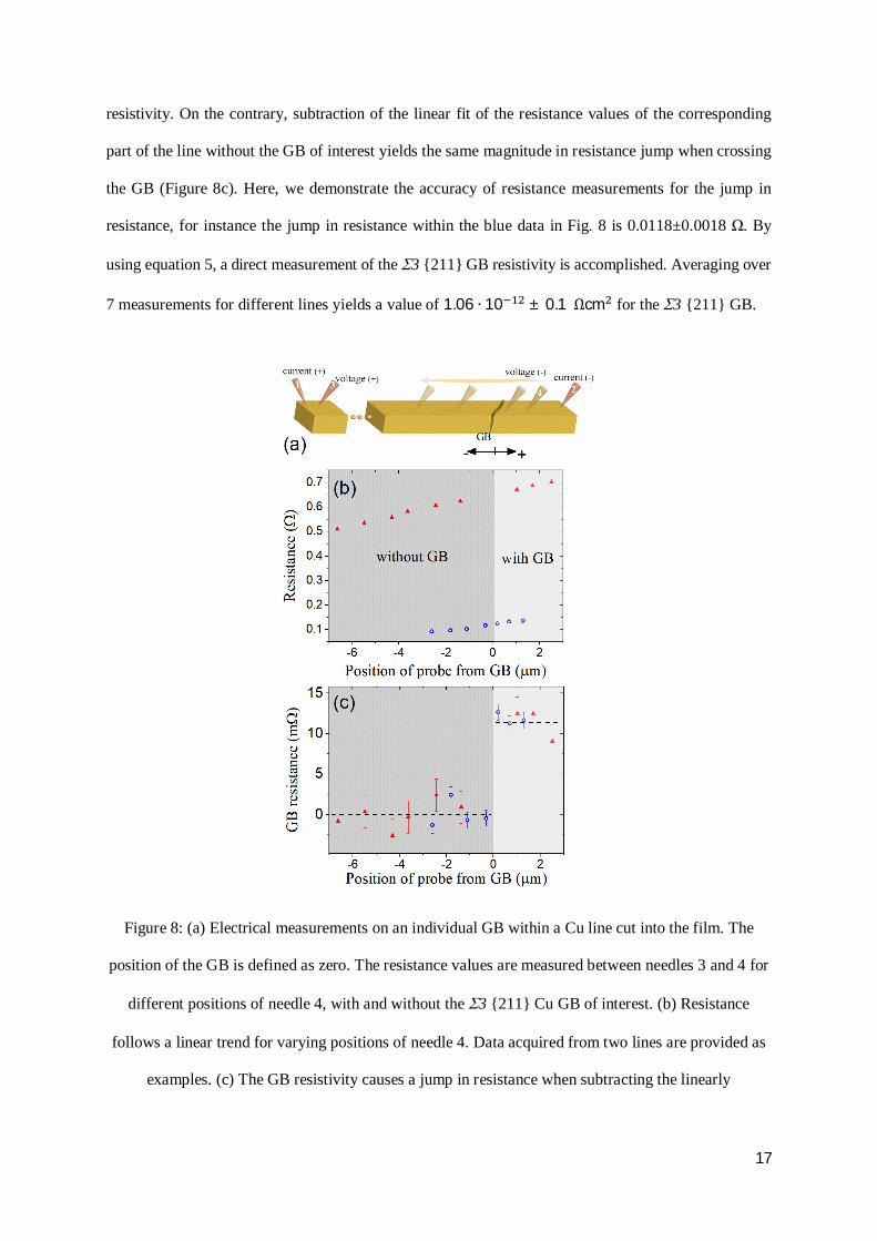
resistivity. On the contrary, subtraction of the linear fit of the resistance values of the corresponding
part of the line without the GB of interest yields the same magnitude in resistance jump when crossing
the GB (Figure 8c). Here, we demonstrate the accuracy of resistance measurements for the jump in
resistance, for instance the jump in resistance within the blue data in Fig. 8 is 0.0118±0.0018 Ω. By
using equation 5, a direct measurement of the S3 {211} GB resistivity is accomplished. Averaging over
7 measurements for different lines yields a value of 1.06 ∙ 10 ± 0.1 Ωcm for the S3 {211} GB.
Figure 8: (a) Electrical measurements on an individual GB within a Cu line cut into the film. The
position of the GB is defined as zero. The resistance values are measured between needles 3 and 4 for
different positions of needle 4, with and without the S3 {211} Cu GB of interest. (b) Resistance
follows a linear trend for varying positions of needle 4. Data acquired from two lines are provided as
examples. (c) The GB resistivity causes a jump in resistance when subtracting the linearly

18
extrapolated resistance of the single grain region of the line from the data containing the GB. The data
from both Cu lines coincide in GB resistance for the incoherent S3 {211} Cu GB.
The measured value of S3 GB resistivity (1.06 ∙ 10 ± 0.1 Ωcm ) matches the order of magnitude
of the average GB resistivity reported for Cu which is in range of (0.15 − 4) ∙ 10 [1, 5, 20,
21,24]. For a Cu coherent S3 GB, DFT calculations reported resistivity of 0.2 ∙ 10 [20, 21].
Our measured value is higher than the calculated prediction due to several reasons:
- The measurements are performed at room temperature in which electron-phonon interaction is
a major scattering mechanism, while this interaction is neglected in the calculation.
- Difference in resistivity between coherent and incoherent S3 GBs due to different atomic
structure at the GB.
- In addition, possible enrichment of Ga at the GB introduced by FIB milling may also affect the
resistivity, although earlier studies indicate that Ga did not enrich at GBs in the lines within the
reported resolution limit of 0.5 at.% [13]. According to the phase diagram, Ga solubility in Cu
exceeds 10 at.% at room temperature [40, 41]. But, usually thermodynamic equilibrium is not
achieved after FIB milling. Hence some accumulation of Ga at GBs is still possible and might
affect the measured GB resistivity [14], but was too low to be resolved by SEM-EDS.
4.2 Electrical resistivity of GBs in bulk Cu
The bicrystal with the asymmetric S5 GB was measured on the common {100} surface using both
approaches, the Van der Pauw and the in-situ 4-point-probe technique. For the Van der Pauw method
the 4 contacts are positioned as described in section 2.3.2. Figure 9a shows a photograph of the bicrystal,
the 4 contacts, and as an artificially coloured overlay the information of the SEM-EBSD grain map
revealing the GB position. The average resistivity value of the single crystal is subtracted from the
average resistivity value of the bicrystal to obtain the contribution of the asymmetric S5 GB to the
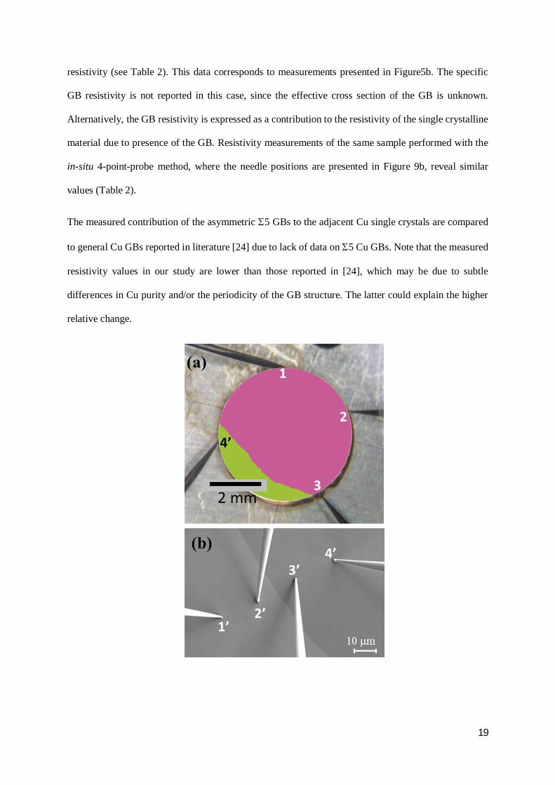
19
resistivity (see Table 2). This data corresponds to measurements presented in Figure5b. The specific
GB resistivity is not reported in this case, since the effective cross section of the GB is unknown.
Alternatively, the GB resistivity is expressed as a contribution to the resistivity of the single crystalline
material due to presence of the GB. Resistivity measurements of the same sample performed with the
in-situ 4-point-probe method, where the needle positions are presented in Figure 9b, reveal similar
values (Table 2).
The measured contribution of the asymmetric S5 GBs to the adjacent Cu single crystals are compared
to general Cu GBs reported in literature [24] due to lack of data on S5 Cu GBs. Note that the measured
resistivity values in our study are lower than those reported in [24], which may be due to subtle
differences in Cu purity and/or the periodicity of the GB structure. The latter could explain the higher
relative change.

20
Figure 9: (a) Van der Pauw contacts of the Cu bicrystal. The colour code indicates the two grains
based on SEM-EBSD measurement. (b) In-situ 4-point probe measurements across an individual GB
in the bulk Cu.
Table 2: Contribution of an individual asymmetric S5 GB in Cu to the resistivity of the adjacent single
crystal measured by Van der Pauw and 4-point-probe techniques. Difference between bicrystal and
single crystal resistivities are presented. The average values reported in literature are presented for
comparison.
GB typeGB resistivity contribution to adjacent Cu single crystal
Absolute value (mW cm) Relative value (%)
asym. S5 (Van der Pauw) 0.052 ± 0.007 3.07 ± 0.4
asym. S5 (4-point probe) 0.048 ± 0.007 2.84 ± 0.4
Twin GB – Literature [24] 0.07 4.19
High angle GB– Literature [24] 0.14 8.38
5. Conclusions
In this work, we provide protocols for direct local electrical resistivity measurements of individual GB
in thin metallic films and bulk metals using Cu as a case study. The results demonstrate the capability
to directly measure the resistivity of a single CSL GB in a highly conductive material by combining
precise electrical measurements, different contacting techniques, and suitable sample structures. The
samples require currently grain sizes of >6µm to enable precise positioning of the contacts. Electrical
measurements are carried out using dc pulses to avoid noise caused by Joule heating and contact drift.
Resistivity of an asymmetric S5 Cu GB is measured in a bulk Cu sample using the Van der Pauw
method as well as the local in-situ 4-point-probe technique. Resistivity values obtained by both

21
techniques are in agreement. In addition, we were able to resolve the resistivity of a single incoherent
S3 Cu GB in a thin film. The latter measurement is performed on lines within the film produced by FIB
milling. The methodology described in this paper will enable systematic studies on relationships
between GB resistivity and their structure in metals.
6. Acknowledgements
H.B. acknowledges the financial support by the ERC Advanced Grant GB CORRELATE (Grant
Agreement 787446 GB-CORRELATE) of G.D.
References
1. Andrews, P.V., M.B. West, and C.R. Robeson, The effect of grain boundaries on the electrical
resistivity of polycrystalline copper and aluminium. The Philosophical Magazine: A Journal of
Theoretical Experimental and Applied Physics, 1969. 19(161): p. 887-898.
2. Mayadas, A.F. and M. Shatzkes, Electrical-Resistivity Model for Polycrystalline Films: the
Case of Arbitrary Reflection at External Surfaces. Physical Review B, 1970. 1(4): p. 1382-1389.
3. W. Wu, S. H. Brongersma, M. Van Hove K. Maex, Influence of surface and grain-boundary
scattering on the resistivity of copper in reduced dimensions. Applied Physics Letters, 2004. 84(15):
p. 2838-2840.
4. W. Steinhögl, G. Schindler, G. Steinlesberger, M. Traving, M. Engelhardt, Comprehensive
study of the resistivity of copper wires with lateral dimensions of 100 nm and smaller. Journal of
Applied Physics, 2005. 97(2): p. 023706.
5. Mannan, K.M. and K.R. Karim, Grain boundary contribution to the electrical conductivity of
polycrystalline Cu films. Journal of Physics F: Metal Physics, 1975. 5(9): p. 1687-1693.
6. A. Pyzyna, R. Bruce, M. Lofaro, H. Tsai, C. Witt, L. Gignac, M. Brink, M. Guillorn, G. Fritz,
H. Miyazoe, D. Klaus, E. Joseph, K. P. Rodbell, C. Lavoie, D. Park, Resistivity of copper
interconnects beyond the 7 nm node. in 2015 Symposium on VLSI Technology (VLSI Technology).
2015.

22
7. Felipe Cemina, Daniel Lundin, Davide Cammilleri, Thomas Maroutian, Philippe Lecoeur,
Tiberiu Minea, Low electrical resistivity in thin and ultrathin copper layers grown by high power
impulse magnetron sputtering. Journal of Vacuum Science & Technology A, 2016. 34(5): p. 051506.
8. Raul C. Munoz1, Claudio Arenas, Size effects and charge transport in metals: Quantum
theory of the resistivity of nanometric metallic structures arising from electron scattering by grain
boundaries and by rough surfaces, Applied Physics Reviews, 2017, 4, 011102 (2017)
9. Nicolas J. Peter, Timofey Frolov, Maria J. Duarte, Raheleh Hadian, Colin Ophus, Christoph
Kirchlechner, Christian H. Liebscher, and Gerhard Dehm, Segregation-Induced Nanofaceting
Transition at an Asymmetric Tilt Grain Boundary in Copper. Physical Review Letters, 2018. 121(25):
p. 255502.
10. Christian H. Liebscher, Andreas Stoffers, Masud Alam, Liverios Lymperakis, Oana Cojocaru-
Mirédin, Baptiste Gault, Jörg Neugebauer, Gerhard Dehm, Christina Scheu, and Dierk Raabe, Strain-
Induced Asymmetric Line Segregation at Faceted Si Grain Boundaries. Physical Review Letters,
2018. 121(1): p. 015702.
11. Qiang Zhu, Amit Samanta, Bingxi Li, Robert E. Rudd, Timofey Frolov, Predicting phase
behavior of grain boundaries with evolutionary search and machine learning. Nature
Communications, 2018. 9(1): p. 467.
12. T. Frolov, W. Setyawan, R. J. Kurtz, J. Marian, A. R. Oganov, R. E. Rudd, Q. Zhu, Grain
boundary phases in bcc metals. Nanoscale, 2018. 10(17): p. 8253-8268.
13. N.V. Malyar, B. Grabowski, G. Dehm, C. Kirchlechner, Dislocation slip transmission through
a coherent Σ3{111} copper twin boundary: Strain rate sensitivity, activation volume and strength
distribution function. Acta Materialia, 2018. 161: p. 412-419.
14. Tae-Hwan Kim, Don M. Nicholson, X.-G. Zhang, Boyd M. Evans, Nagraj S. Kulkarni,
Edward A. Kenik, Harry M. Meyer, Balasubramaniam Radhakrishnan, An-Ping Li, Structural
Dependence of Grain Boundary Resistivity in Copper Nanowires. Japanese Journal of Applied
Physics, 2011. 50(8): p. 08LB09.
15. Tae-Hwan Kim, X.-G. Zhang, Don M. Nicholson, Boyd M. Evans, Nagraj S. Kulkarni, B.
Radhakrishnan, Edward A. Kenik, and An-Ping Li, Large Discrete Resistance Jump at Grain
Boundary in Copper Nanowire. Nano Letters, 2010. 10(8): p. 3096-3100.
16. Yusuke Kitaoka, Takeshi Tono, Shinya Yoshimoto, Toru Hirahara, Shuji Hasegawa,
Takayuki Ohba, Direct detection of grain boundary scattering in damascene Cu wires by nanoscale
four-point probe resistance measurements. Applied Physics Letters, 2009. 95(5): p. 052110.
23
17. Nakamichi, I., Electrical Resistivity and Grain Boundaries in Metals. Materials Science
Forum, 1996. 207-209: p. 47-58.
18. Brandon, D.G., The structure of high-angle grain boundaries. Acta Metallurgica, 1966.
14(11): p. 1479-1484.
19. César, M., D. Gall, H. Guo, Reducing Grain-Boundary Resistivity of Copper Nanowires by
Doping. Physical Review Applied, 2016. 5(5): p. 054018.
20. Mathieu César, Dongping Liu, Daniel Gall, Hong Guo, Calculated Resistances of Single
Grain Boundaries in Copper. Physical Review Applied, 2014. 2(4): p. 044007.
21. Daniel Valencia, Evan Wilson, Zhengping Jiang, Gustavo A. Valencia-Zapata, Kuang-Chung
Wang, Gerhard Klimeck, Michael Povolotskyi, Grain-Boundary Resistance in Copper Interconnects:
From an Atomistic Model to a Neural Network, Physical Review Applied, 2018, 9, 044005
22. Gyuseok Kim, Xuzhao Chai, Le Yu, Xuemei Cheng, Daniel S.Gianola, Interplay between
grain boundary segregation and electrical resistivity in dilute nanocrystalline Cu alloys. Scripta
Materialia, 2016. 123: p. 113-117.
23. Kasen, M.B., Grain boundary resistivity of aluminium. The Philosophical Magazine: A
Journal of Theoretical Experimental and Applied Physics, 1970. 21(171): p. 599-610.
24. Lei Lu, Yongfeng Shen, Xianhua Chen, Lihua Qian, K Lu, Ultrahigh Strength and High
Electrical Conductivity in Copper. Science, 2004. 304(5669): p. 422-426.
25. I. Bakonyi, V.A. Isnaini, T. Kolonits, Zs. Czigány, J. Gubicza, L.K. Varga, E. TóthKádár, L.
Pogány, L. Péter, H. Ebert, The specific grain-boundary electrical resistivity of Ni,
PHILOSOPHICAL MAGAZINE, 2019, VOL. 99, NO. 9, 1139–1162
26. Bietsch, A. and B. Michel, Size and grain-boundary effects of a gold nanowire measured by
conducting atomic force microscopy. Applied Physics Letters, 2002. 80(18): p. 3346-3348.
27. J. J. Plombona, Ebrahim Andideh, Valery M. Dubin, and Jose Maiz, Influence of phonon,
geometry, impurity, and grain size on Copper line resistivity. Applied Physics Letters, 2006. 89(11):
p. 113124.
28. Nataliya V. Malyar1, Hauke Springer, Jürgen Wichert, Gerhard Dehm and Christoph
Kirchlechner, Synthesis and mechanical testing of grain boundaries at the micro and sub-micro scale.
Materials Testing, 2019. 61(1): p. 5-18.
29. Daniel Gall, Electron mean free path in elemental metals, J. Appl. Phys. (2016) 119, 085101
24
30. Daniel Gall, The search for the most conductive metal for narrow interconnect lines, J. Appl.
Phys. (2020) 127, 050901
31. L. J. Van der Pauw, A method for measuring specific resistivity and hall effect of discs of
arbitrary shapes. Philips Res. Repts, 1958. 13: p. 1-9.
32. I Miccoli1, F Edler, H Pfnür,C Tegenkamp, The 100th anniversary of the four-point probe
technique: the role of probe geometries in isotropic and anisotropic systems. Journal of Physics:
Condensed Matter, 2015. 27(22): p. 223201.
33. Martin, N., J. Sauget, T. Nyberg, Anisotropic electrical resistivity during annealing of
oriented columnar titanium films. Materials Letters, 2013. 105: p. 20-23.
34. T.Meiners, J. M. Duarte, G. Richter, G.Dehm, C. H. Liebscher, Tantalum and Zirconium
induced structural transitions at complex [111] tilt grain boundaries in Copper. Acta Materialia, 190
(2020) 93-104
35. S.W. Hieke, B. Breitbach, G. Dehm, C. Scheu, Microstructural evolution and solid state
dewetting of epitaxial Al thin films on sapphire (a-Al2O3), Acta Materialia 133 (2017) 356-366
36. Yong Chan Cho, Seunghun Lee, Muhammad Ajmal, Won-Kyung Kim, Chae Ryong Cho, Se-
Young Jeong, Jeung Hun Park, Sang Eon Park, Sungkyun Park, Hyuk-Kyu Pak, Hyoung Chan Kim,
Copper Better than Silver: Electrical Resistivity of the Grain-Free Single-Crystal Copper Wire.
Crystal Growth & Design, 2010. 10(6): p. 2780-2784.
37. E. A. Brandes, G. B. Brook, Smithells Metals Reference Book (Butterworth-Heinemann,
Oxford, 1998).
38. G. Dehm, M. Rühle, G. Ding, R. Raj, Growth and structure of copper thin films deposited on
(0001) sapphire by molecular beam epitaxy. Philosophical Magazine B, 1995. 71(6): p. 1111-1124.
39. G. Dehm, H. Edongué, T. Wagner, S.H. Oh, E. Arzt, Obtaining different orientation
relationships for Cu films grown on (0001) α-Al 2 O 3 substrates by magnetron sputtering. Zeitschrift
für Metallkunde, 2005. 96: p. 249-254.
40. Jendrzejczyk-Handzlik, D., K. Fitzner, W. Gierlotka, On the Cu–Ga system: Electromotive
force measurement and thermodynamic reoptimization. Journal of Alloys and Compounds, 2015. 621:
p. 287-294.
41. Muzzillo, C.P., C.E. Campbell, T.J. Anderson, Cu–Ga–In thermodynamics: experimental
study, modeling, and implications for photovoltaics. Journal of Materials Science, 2016. 51(7): p.
3362-3379.