differential amplifier applications large signal input...
TRANSCRIPT

Lecture 8 Overview• Differential Amplifier
– Applications– Large Signal Input-Output Characteristic– Preview Symmetry Analysis: "Half Circuit”– Active (Mirror) Load– Text: Sec. 3.8 pp. 142-146

ECG: Electrocardiogram• Display electrical activity
of heart muscle• Shape of waveform
related to health of heart

ECG: Electrocardiogram
• Shape of waveform related to health of heart• Amplitude: mV range• Problem: Can’t contact VH directly• Access only to voltage waveform on surface:

Voltage waveform on surface
• 60Hz inteference: body acts as 60 Hz antenna!• How to recover signal?
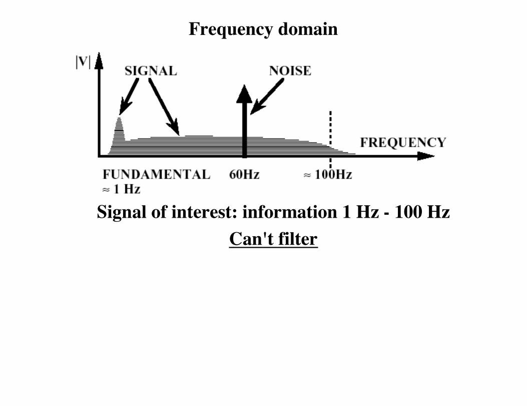
Frequency domain
Signal of interest: information 1 Hz - 100 HzCan't filter
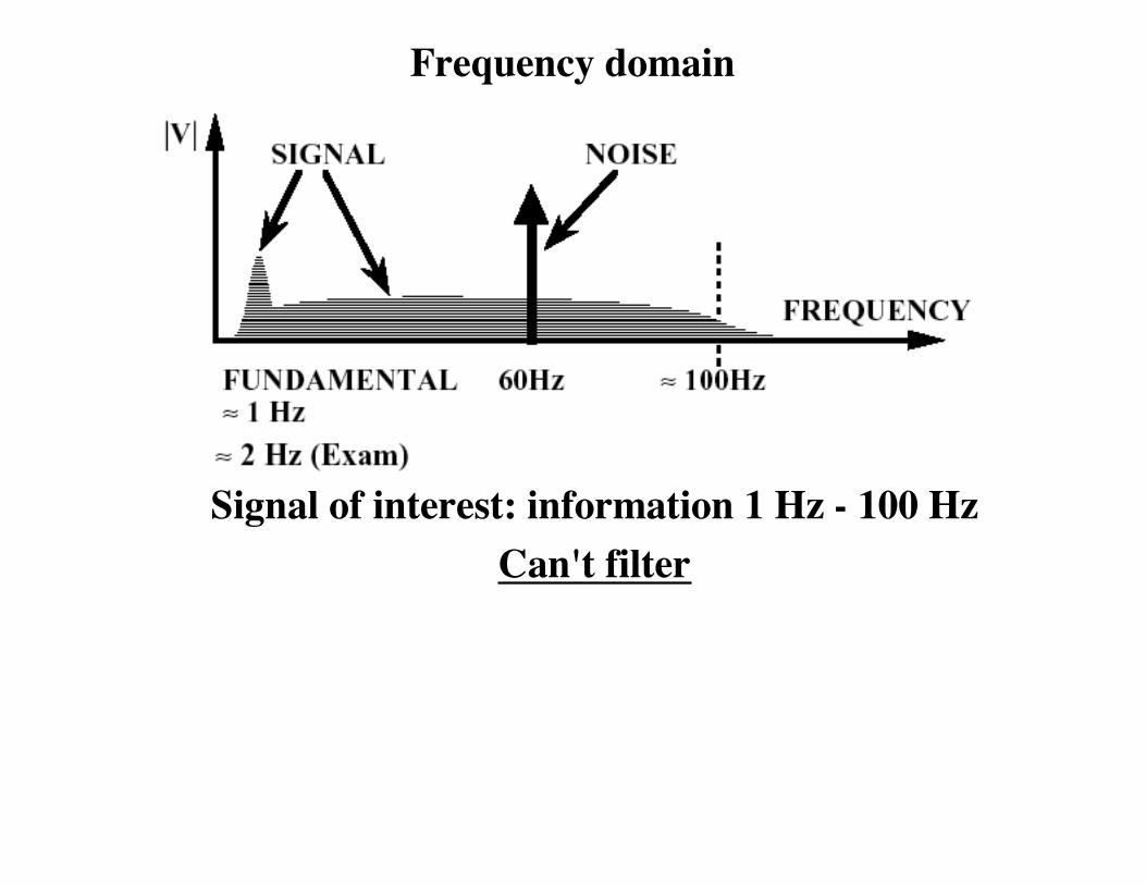
Frequency domain
Signal of interest: information 1 Hz - 100 HzCan't filter

Frequency domain
Signal of interest: information 1 Hz - 100 HzCan't filter

Alternative approach• VS1 = 60Hz
+ Desired Signal• Second electrode
far from heart• VS2 = 60Hz

Subtract Waveforms
VS1 = 60Hz + Desired Signal VS2 = 60HzVS1 - VS2= Desired Signal (60Hz subtracted out)

Differential Amplifier Function• Desired signal is small (mV range)• Required function: Vout = AV(diff)[VS1 - VS2]• AV(diff): "Differential Gain"• Difference amplified• Common mode rejected (subtracted out)
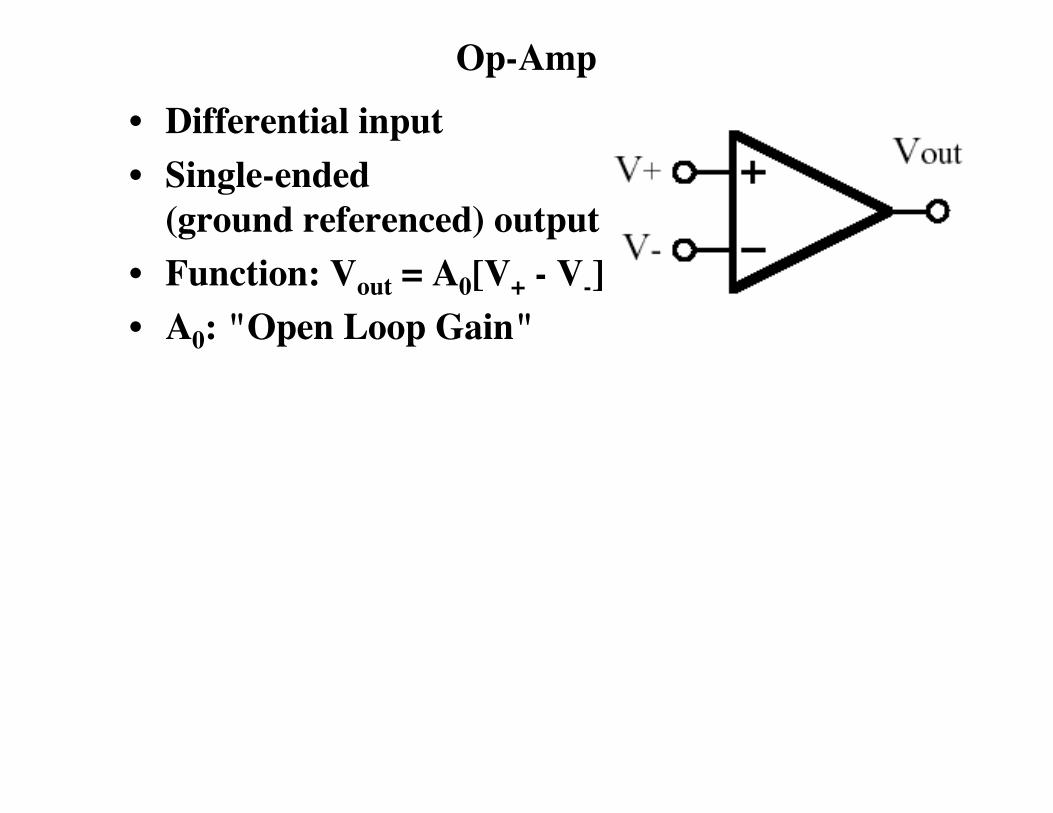
Op-Amp• Differential input• Single-ended
(ground referenced) output• Function: Vout = A0[V+ - V-]• A0: "Open Loop Gain"

Circuit: Differential Amplifier (Resistive Load)• "Source-Coupled Pair"Analysis strategy• Large-signal
– DC Bias– Input-output
characteristic• Small-signal gain
VDD
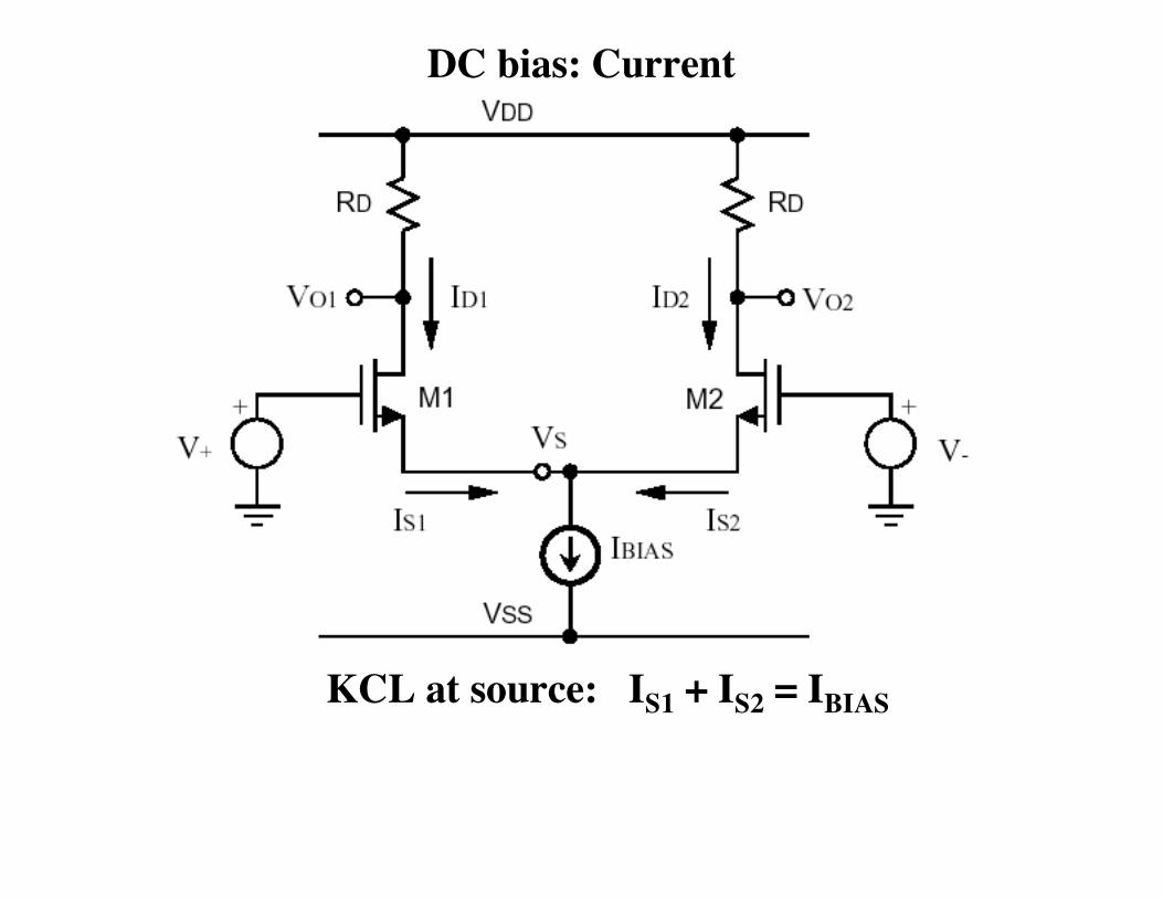
DC bias: Current
KCL at source: IS1 + IS2 = IBIAS

DC bias: Current
• KCL at source:IS1 + IS2 = IBIAS
• For MOSFET:Gate IG = 0 (oxide)Substrate IB = 0(reverse bias junction)
Source,drain currents equal: IS = ID

KCL Result• ID1 + ID2 = IBIAS
• MOSFET pair"splits" bias current
• Total must equal IBIAS• Split determined
by VGS1, VGS2• Current source bias: VS will be whatever
necessary to make correct VGS values

VGS values• KVL path
V+ -VGS1 + VGS2 = V-
V+ -V-DIFFINPUT
1 2 4 3 4 = VGS1 - VGS2
DVGS1 2 4 3 4

Build up V-I characteristic
• Focus on ID1, ID2
• Assume active region(always check Vout, VGD)
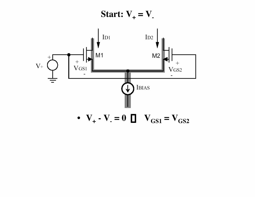
Start: V+ = V-
• V+ - V- = 0 fi VGS1 = VGS2

Start: V+ = V-
• V+ - V- = 0 fiVGS1 = VGS2
• M1, M2 active• Identical devices
fi Identical conditionsVGS1 = VGS2 fiIdentical behavior fi ID1 = ID2
• KCL: ID1 + ID2 = IBIAS
ID1 = ID2 = IBIAS / 2Differential pair "balanced"
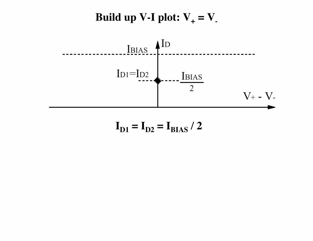
Build up V-I plot: V+ = V-
ID1 = ID2 = IBIAS / 2
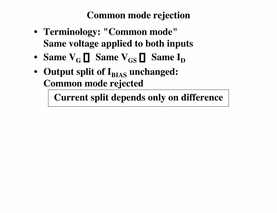
Common mode rejection• Terminology: "Common mode"
Same voltage applied to both inputs• Same VG fi Same VGS fi Same ID
• Output split of IBIAS unchanged:Common mode rejected
Current split depends only on difference

Large differential input: V+ >> V-
Increase V+ >> V-

Large differential input: V+ >> V-
• Increase V+ >> V-
• V+ - V- = VGS1 - VGS2• VGS1 increases,
VGS2 decreases• Eventually VGS2 < Vtn
fi ID2 = 0 (M2 cutoff)M1 gets all the current: ID1 = IBIAS
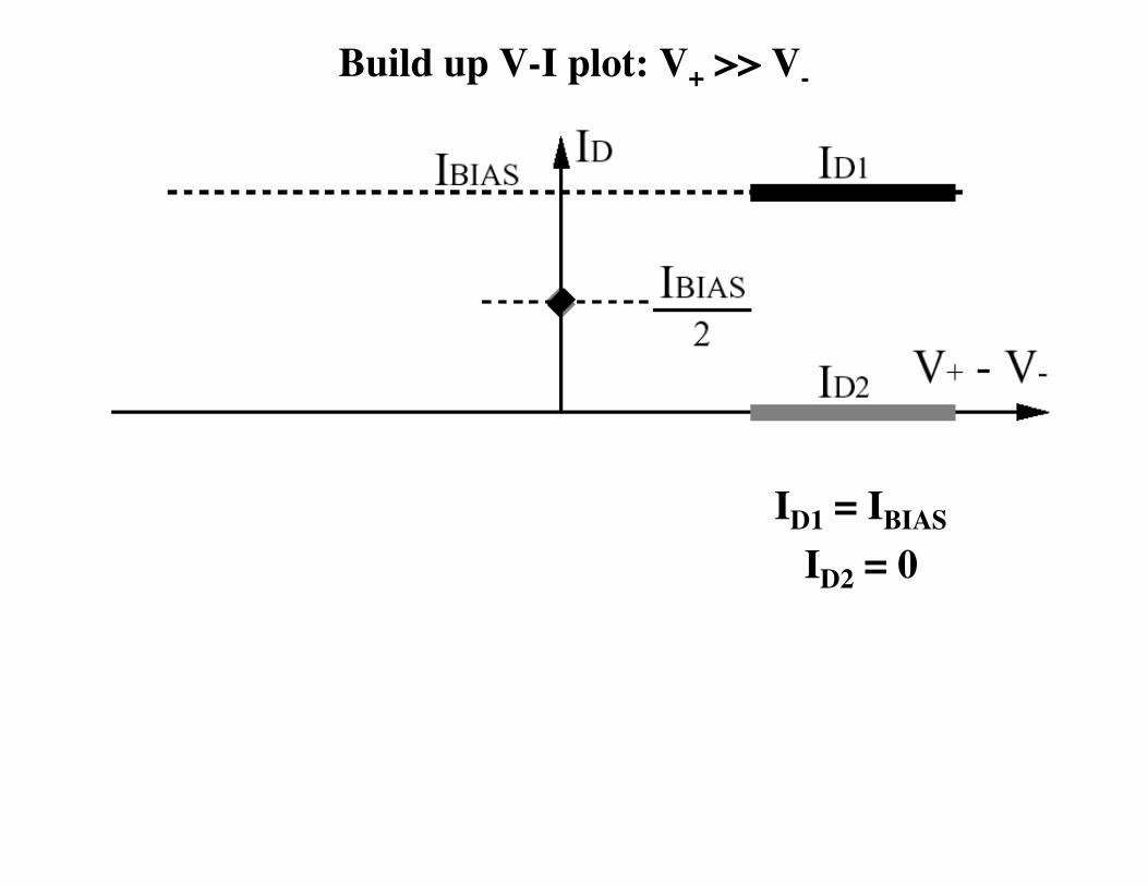
Build up V-I plot: V+ >> V-
ID1 = IBIAS
ID2 = 0

Large differential input: V- >> V+
Increase V- >> V+

Large differential input: V- >> V+
• Increase V- >> V+
• V+ - V- = VGS1 - VGS2• VGS2 increases,
VGS1 decreases• Eventually VGS1 < Vtn
fi ID1 = 0 (M1 cutoff)M1 gets all the current: ID2 = IBIAS

Build up V-I plot: V- >> V+
ID1 = 0ID2 = IBIAS

Finish: "Connect the dots"
• General shape for any differential pair:MOSFET, BJT, JFET, ...
• Specifics depend on bias, technology, etc.
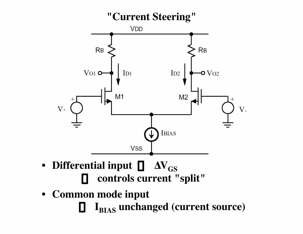
"Current Steering"
• Differential input fi ∆VGS fi controls current "split"
• Common mode input fi IBIAS unchanged (current source)

Voltage OutputKVL paths:
VO1 = VDD - ID1RD VO2 = VDD - ID2RD

Voltage Output
VO1 = VDD - ID1RD VO2 = VDD - ID2RD

Differential Voltage Output: VOD = VO1 - VO2
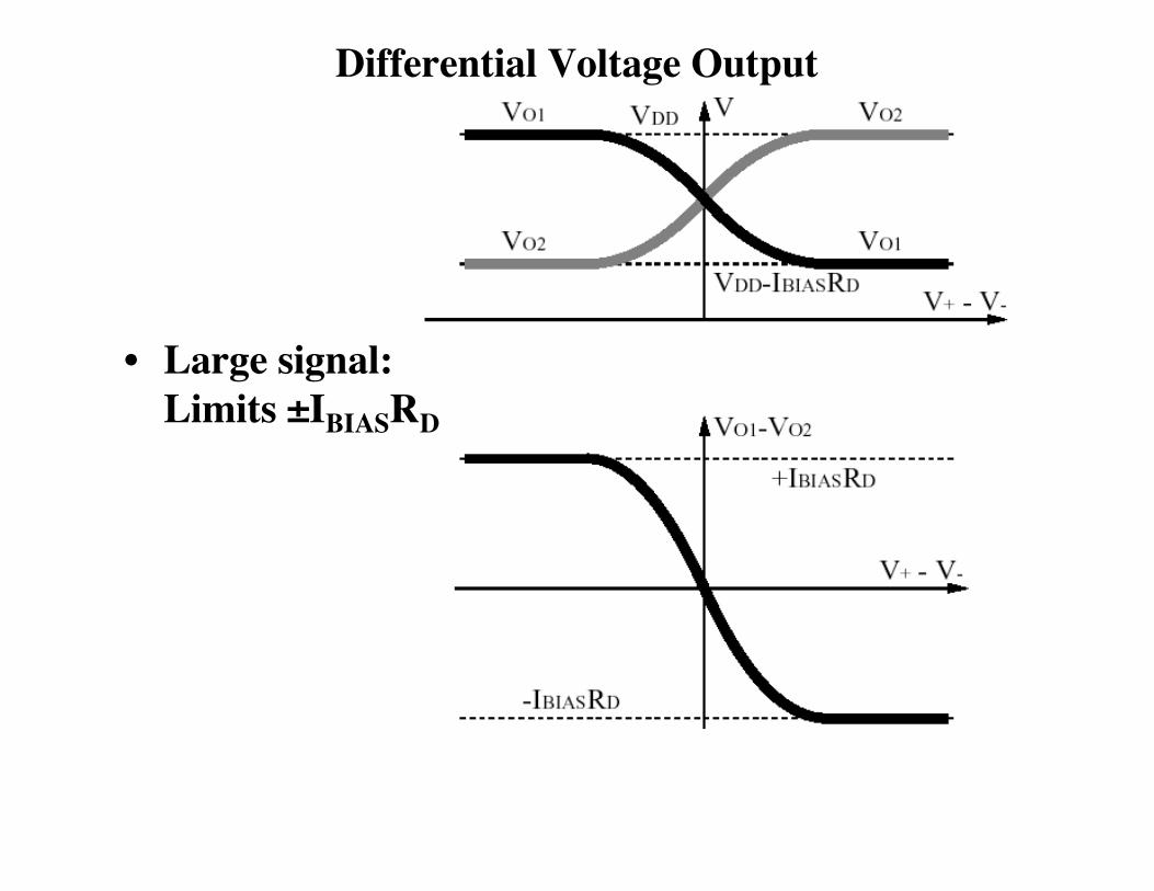
Differential Voltage Output
• Large signal:Limits ±IBIASRD

Differential Voltage Output
• Slope of plot at operating point (origin):Small signal differential gain av(diff)
Differential Gain• Need to improve fi need to be quantitative• Analytic tool:
Bartlett's Bisection Theorem• Applies for symmetrical circuits• Simplifies analysis:
Allows splitting of circuit into separate halves
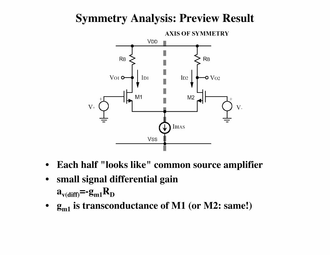
Symmetry Analysis: Preview Result
• Each half "looks like" common source amplifier• small signal differential gain
av(diff)=-gm1RD
• gm1 is transconductance of M1 (or M2: same!)

Bartlett's Bisection Theorem• Two completely symmetrical circuits
a, b, c are connected points of symmetry
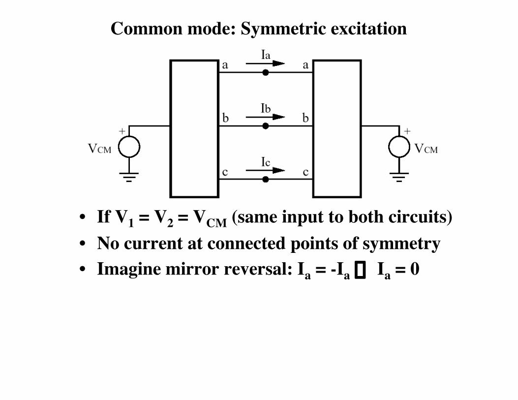
Common mode: Symmetric excitation
• If V1 = V2 = VCM (same input to both circuits)• No current at connected points of symmetry• Imagine mirror reversal: Ia = -Ia fi Ia = 0

Common mode: Symmetric excitation
• We can open all leads between connected pointsof symmetry without affecting circuit operation
• Applies for any circuit (linear or nonlinear)

Differential mode: Antisymmetric excitation
If V1 = -V2 : “See-Saw”:Fixed voltage at connected points of symmetry
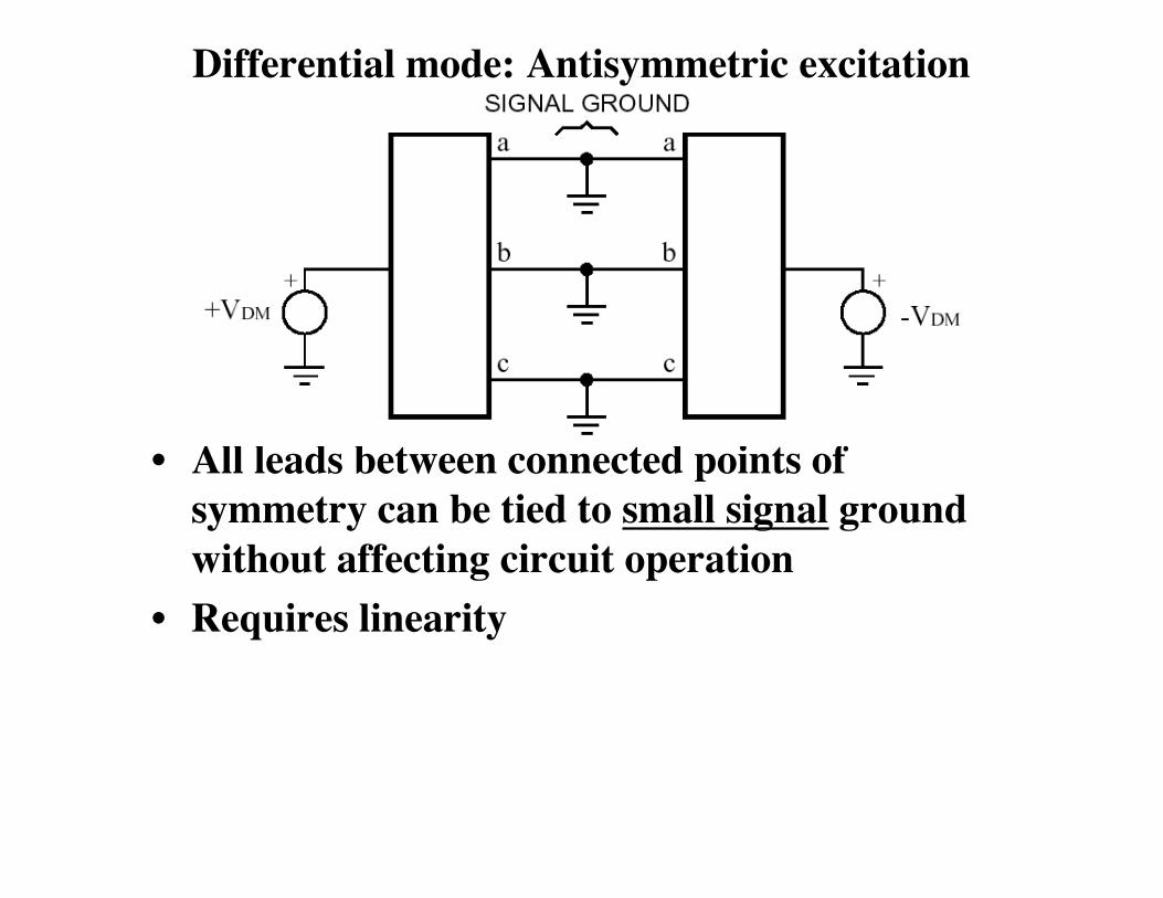
Differential mode: Antisymmetric excitation
• All leads between connected points ofsymmetry can be tied to small signal groundwithout affecting circuit operation
• Requires linearity

Bartlett's Bisection Theorem• Applies to symmetric circuits• Common mode (symmetric) excitation
– Open connected points of symmetry• Differential (antisymmetric) excitation
– Connected points of symmetry tied to signalground
– Requires linearity

Any two signals!
Can be expressed as sum ofcommon mode, differential mode:

Any two signals!
• Define:
• Can verify:
VCM =V1 + V2
2Vdm = V1 - V2
V1 = VCM +Vdm
2
V 2 = VCM -Vdm
2

Half circuit analysis technique1) Represent inputs in terms of Vdm, Vcm
2) Redraw circuit to emphasize symmetry3) Use superposition to find output:
– DC bias: V1, V2 = 0 (all inputs suppressed)– CM Response: keep vCM , set vdm = 0– DM response: keep vdm , set vCM = 0– Add results for total output
• Split circuit using bisection theorem:– Analyze each half separately

1) Represent inputs in terms of Vdm, Vcm
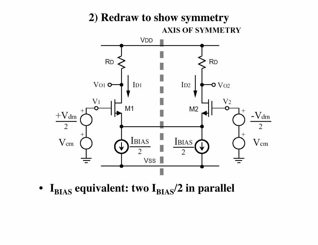
2) Redraw to show symmetry
• IBIAS equivalent: two IBIAS/2 in parallel

DC bias: V1, V2 = 0 (all signal inputs suppressed)
• Symmetric excitation:open connected points of symmetry
VO1(DC ) = VDD -IBIAS
2RD VO2(DC) = VDD -
IBIAS2
RD
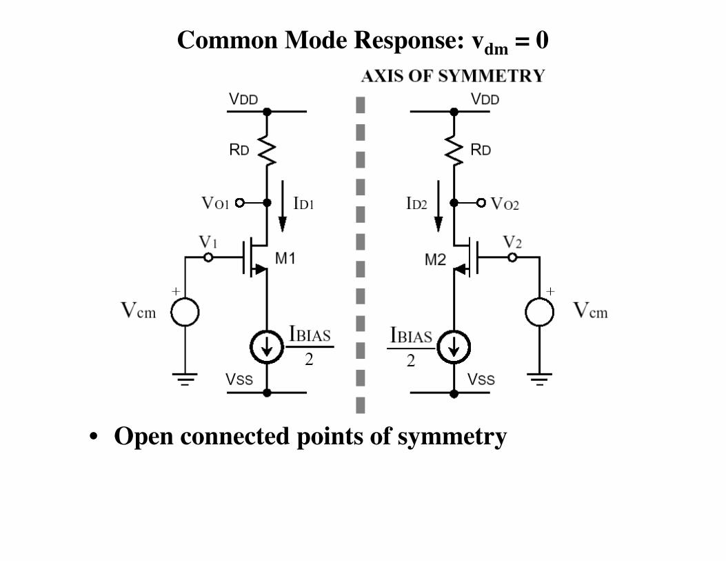
Common Mode Response: vdm = 0
• Open connected points of symmetry

Note "supernode": id = 0
Vo1(cm) = -idRD = 0 Vo2(cm) = 0

Differential mode response: vcm = 0
• Connected points of symmetry to signal ground

Small signal model of half-circuit
• Common source amplifier!• Note: gm1 = gm2 = gm
Vo1(dm )OUTPUT1 2 3
= -gmRDvdm
2INPUT
Vo2(dm)OUTPUT1 2 4 3 4
= -gm RD-vdm
2INPUT1 2 3

Summary: Output “parts”
• DC bias
• Commonmode
• Differentialmode
Vo1(dm ) =-gmRD
2vdm Vo2(dm) =
gmRD2
vdm
Vo1(cm) = 0 Vo2(cm) = 0
VO1(DC ) = VDD -IBIAS
2RD VO2(DC) = VDD -
IBIAS2
RD

Summary: Total output sum of components
VO1 = VDD -IBIAS
2RD
DCBIAS1 2 4 4 3 4 4
+ 0CM
+-gmRD
2vdm
DIFFERENTIALMODE
1 2 4 3 4
VO2 = VDD -IBIAS
2RD
DCBIAS1 2 4 4 3 4 4
+ 0CM
+gmRD
2vdm
DIFFERENTIALMODE
1 2 4 3 4
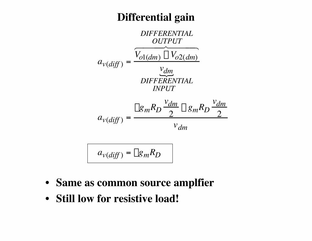
Differential gain
• Same as common source amplfier• Still low for resistive load!
av(diff ) =Vo1(dm) - Vo2(dm)
DIFFERENTIALOUTPUT6 7 4 4 4 8 4 4 4
vdmDIFFERENTIAL
INPUT
av(diff ) =-gmRD
vdm2
- gmRDvdm
2vdm
av(diff ) = -gmRD
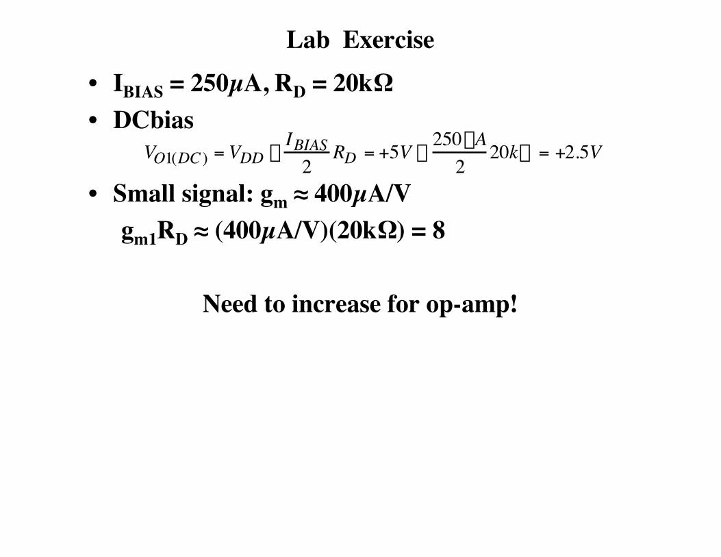
Lab Exercise• IBIAS = 250µA, RD = 20kΩ• DCbias
• Small signal: gm ≈ 400µA/Vgm1RD ≈ (400µA/V)(20kΩ) = 8
Need to increase for op-amp!
VO1(DC ) = VDD -IBIAS
2RD = +5V -
250mA2
20kW = +2.5V

Drain Currents

Mirror load
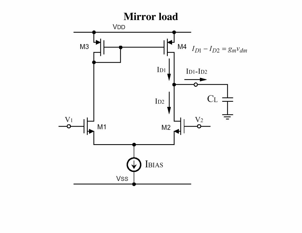
Mirror load
ID1 - ID2 = gmvdm

Mirror load
• Gain increased• Similar to result
for commonsource, active load

Lecture 8 Summary• Differential Amplifier
– "Build up" Large Signal Input-OutputCharacteristic
– Key: M1, M2 identical– Differential Input controls ”split" of IBIAS– Common mode input rejected
• Symmetry Analysis: "Half Circuit"– Bartlett's Bisection Theorem
• Mirror Load– Increased gain (active load)– Single ended output without 1/2 factor loss
(mirror)