lecture 190 – differential amplifier
TRANSCRIPT
Lecture 190 – Differential Amplifier (3/27/10) Page 190-1
CMOS Analog Circuit Design © P.E. Allen - 2010
LECTURE 190 – DIFFERENTIAL AMPLIFIERLECTURE ORGANIZATION
Outline• Characterization of a differential amplifier• Differential amplifier with a current mirror load• Differential amplifier with MOS diode loads• An intuitive method of small signal analysis• Large signal performance of differential amplifiers• Differential amplifiers with current source loads• Design of differential amplifiers• SummaryCMOS Analog Circuit Design, 2nd Edition ReferencePages 180-199
Lecture 190 – Differential Amplifier (3/27/10) Page 190-2
CMOS Analog Circuit Design © P.E. Allen - 2010
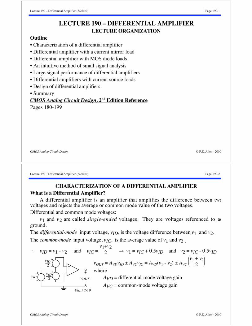
CHARACTERIZATION OF A DIFFERENTIAL AMPLIFIERWhat is a Differential Amplifier?
A differential amplifier is an amplifier that amplifies the difference between twovoltages and rejects the average or common mode value of the two voltages.Differential and common mode voltages:
v1 and v2 are called single-ended voltages. They are voltages referenced to acground.The differential-mode input voltage, vID, is the voltage difference between v1 and v2.
The common-mode input voltage, vIC, is the average value of v1 and v2 .
vID = v1 - v2 and vIC = v1+v2
2 v1 = vIC + 0.5vID and v2 = vIC - 0.5vID
vOUT = AVDvID ± AVCvIC = AVD(v1 - v2) ± AVC v1 + v2
2
whereAVD = differential-mode voltage gain
AVC = common-mode voltage gain
+- +
vOUT
-
vIC
vID2
vID2
Fig. 5.2-1B
Lecture 190 – Differential Amplifier (3/27/10) Page 190-3
CMOS Analog Circuit Design © P.E. Allen - 2010
Differential Amplifier Definitions• Common mode rejection rato (CMRR)
CMRR = AVDAVC
CMRR is a measure of how well the differential amplifier rejects the common-modeinput voltage in favor of the differential-input voltage.• Input common-mode range (ICMR)
The input common-mode range is the range of common-mode voltages over whichthe differential amplifier continues to sense and amplify the difference signal with thesame gain.Typically, the ICMR is defined by the common-mode voltage range over which allMOSFETs remain in the saturation region.
• Output offset voltage (VOS(out))
The output offset voltage is the voltage which appears at the output of the differentialamplifier when the input terminals are connected together.• Input offset voltage (VOS(in) = VOS)
The input offset voltage is equal to the output offset voltage divided by the differentialvoltage gain.
VOS = VOS(out)
AVD
Lecture 190 – Differential Amplifier (3/27/10) Page 190-4
CMOS Analog Circuit Design © P.E. Allen - 2010
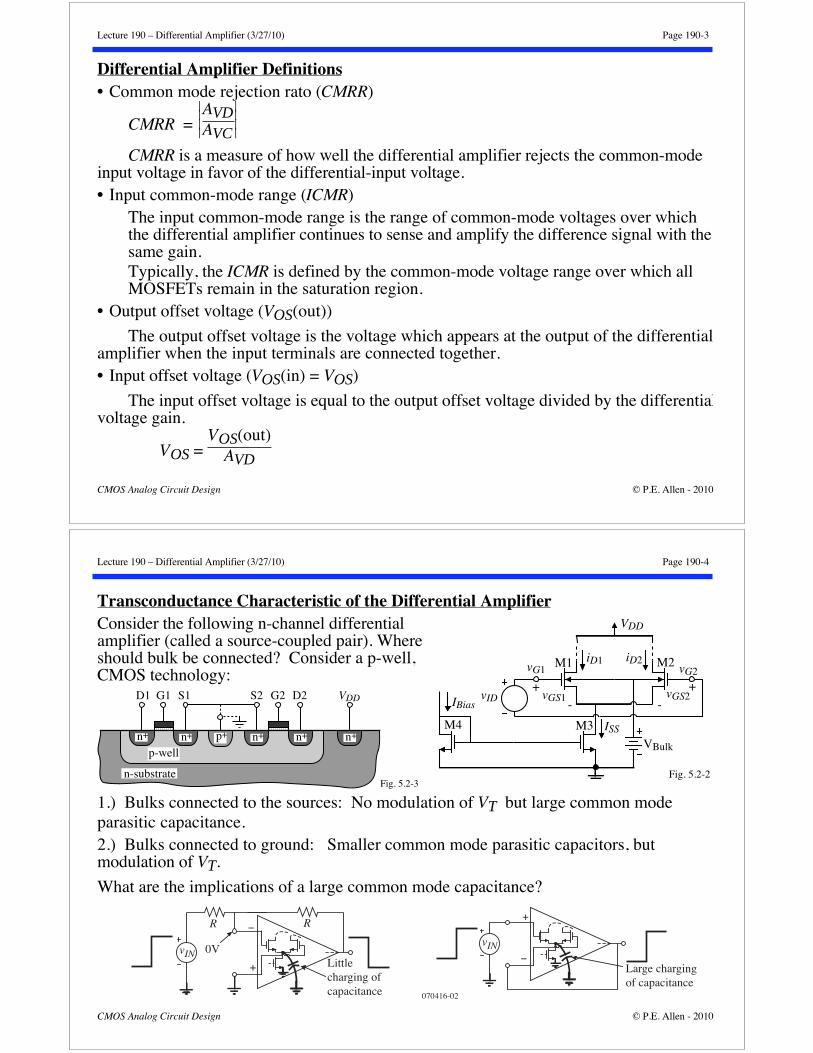
Transconductance Characteristic of the Differential AmplifierConsider the following n-channel differentialamplifier (called a source-coupled pair). Whereshould bulk be connected? Consider a p-well,CMOS technology:
�yD1 G1 S1 �yS2 G2 D2
n+ n+ n+ n+ n+p+
p-well
n-substrate
VDD
Fig. 5.2-3
1.) Bulks connected to the sources: No modulation of VT but large common modeparasitic capacitance.2.) Bulks connected to ground: Smaller common mode parasitic capacitors, butmodulation of VT.
What are the implications of a large common mode capacitance?
IBias
iD1 iD2
VDD
VBulk
M1 M2
M3M4 ISS
+-
vG1
vGS1+
-vGS2
vG2
Fig. 5.2-2
vID
+
−R R
0V
+
−vINvIN
Littlecharging ofcapacitance
Large charging of capacitance
070416-02
Lecture 190 – Differential Amplifier (3/27/10) Page 190-5
CMOS Analog Circuit Design © P.E. Allen - 2010
Transconductance Characteristic of the Differential Amplifier - ContinuedDefining equations:
vID = vGS1 vGS2 = 2iD1 1/2
2iD2 1/2
and ISS = iD1 + iD2
Solution:
iD1 = ISS2 +
ISS2
v2ID
ISS
2v4ID
4I2SS
1/2and iD2 =
ISS2
ISS2
v2ID
ISS
2v4ID
4I2SS
1/2
which are valid for vID < 2(ISS/ )1/2.Illustration of the result:
Differentiating iD1 (or iD2)with respect to vID andsetting VID =0V gives
gm = diD1dvID(VID = 0) =
bISS4 =
K'1ISSW14L1 (half the gm of an inverting amplifier)
iD/ISS
0.8
0.2
0.0
1.0
0.6
0.4
1.414 2.0-1.414-2.0vID
(ISS/ß)0.5
iD1
iD2
Fig. 5.2-4
Lecture 190 – Differential Amplifier (3/27/10) Page 190-6
CMOS Analog Circuit Design © P.E. Allen - 2010
DIFFERENTIAL AMPLIFIER WITH A CURRENT MIRROR LOADVoltage Transfer Characteristic of the Differential Amplifier
In order to obtain the voltage transfer characteristic, a load for the differential amplifiermust be defined. We will select a current mirror load as illustrated below.
Note that output signal to ground isequivalent to the differential outputsignal due to the current mirror.The short-circuit, transconductance isgiven as
gm = diOUTdvID (VID = 0) = ISS =
K'1ISSW1L1
VBias
ISS
M1 M2
M3 M4
VDD
M5
vGS1+
-vGS2
+-
vG2
-
vOUT
iOUT
vG1
-
iD1 iD2
iD3 iD4
-
+
Fig. 5.2-5
2μm1μm
2μm1μm
2μm1μm
2μm1μm
2μm1μm
VDD2
Lecture 190 – Differential Amplifier (3/27/10) Page 190-7
CMOS Analog Circuit Design © P.E. Allen - 2010
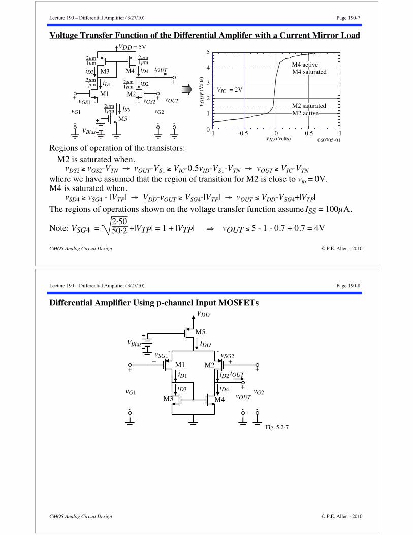
Voltage Transfer Function of the Differential Amplifer with a Current Mirror Load
VBias
ISS
M1 M2
M3 M4
VDD
M5
vGS1+
- vGS2+
-vG2
-
vOUT
iOUT
vG1
-
iD1 iD2
iD3 iD4
-
+2μm1μm
2μm1μm
2μm1μm
2μm1μm
2μm1μm
0
1
2
3
4
5
-1 -0.5 0 0.5 1vID (Volts)
v OU
T (V
olts
)
M2 saturatedM2 active
M4 activeM4 saturated
VIC� = 2V
= 5V
060705-01
Regions of operation of the transistors:M2 is saturated when, vDS2 vGS2-VTN vOUT-VS1 VIC-0.5vID-VS1-VTN vOUT VIC-VTN
where we have assumed that the region of transition for M2 is close to vID = 0V. M4 is saturated when, vSD4 vSG4 - |VTP| VDD-vOUT VSG4-|VTP| vOUT VDD-VSG4+|VTP|
The regions of operations shown on the voltage transfer function assume ISS = 100μA.
Note: VSG4 = 2·5050·2 +|VTP| = 1 + |VTP| vOUT 5 - 1 - 0.7 + 0.7 = 4V
Lecture 190 – Differential Amplifier (3/27/10) Page 190-8
CMOS Analog Circuit Design © P.E. Allen - 2010
Differential Amplifier Using p-channel Input MOSFETs
VBias IDD
M1 M2
M3 M4
VDD
M5
vSG1
+
-vSG2
+
-
vG2
-
vOUT
iOUT
vG1
-
iD1 iD2
iD3 iD4
-
+
Fig. 5.2-7
++
Lecture 190 – Differential Amplifier (3/27/10) Page 190-9
CMOS Analog Circuit Design © P.E. Allen - 2010
Input Common Mode Range (ICMR)ICMR is found by setting vID = 0 and varying vICuntil one of the transistors leaves the saturation.Highest Common Mode VoltagePath from G1 through M1 and M3 to VDD:
VIC(max) =VG1(max) =VG2(max)
=VDD -VSG3 -VDS1(sat) +VGS1or
VIC(max) = VDD - VSG3 + VTN1
Path from G2 through M2 and M4 to VDD:
VIC(max)’ =VDD -VSD4(sat) -VDS2(sat) +VGS2
=VDD -VSD4(sat) + VTN2
VIC(max) = VDD - VSG3 + VTN1
Lowest Common Mode Voltage (Assume a VSS for generality)
VIC(min) = VSS +VDS5(sat) + VGS1 = VSS +VDS5(sat) + VGS2
where we have assumed that VGS1 = VGS2 during changes in the input common modevoltage.
VBias
ISS
M1 M2
M3 M4
VDD
M5
vGS1+
-vGS2
+-
vG2
-
vOUT
iOUT
vG1
-
iD1 iD2
iD3 iD4
-
+
Fig. 330-02
2μm1μm
2μm1μm
2μm1μm
2μm1μm
2μm1μm
VDD2
Lecture 190 – Differential Amplifier (3/27/10) Page 190-10
CMOS Analog Circuit Design © P.E. Allen - 2010
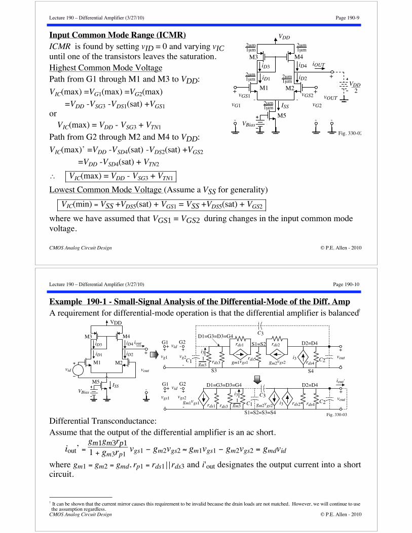
Example 190-1 - Small-Signal Analysis of the Differential-Mode of the Diff. AmpA requirement for differential-mode operation is that the differential amplifier is balanced†
gm3rds3
1
rds1
gm1vgs1
rds2
gm2vgs2
i3i3
+
-
+
-
+G2
vid
vg1 vg2
G1
C1
-
rds5
S1=S2
rds4
C3
C2
+
-
vout
D1=G3=D3=G4
S3 S4
D2=D4
gm3rds31
rds1gm1vgs1 rds2gm2vgs2
i3
i3
+
-
+
-
+G2
vid
vgs1 vgs2
G1
C1
-
S1=S2=S3=S4
rds4
C3C2
+
-
vout
D1=G3=D3=G4 D2=D4iout'
ISS
M1 M2
M3 M4
VDD
M5
vout
iout
iD1 iD2
iD3 iD4
-
+
Fig. 330-03
VBias
vid
Differential Transconductance:Assume that the output of the differential amplifier is an ac short.
iout’ = gm1gm3rp1
1 + gm3rp1 vgs1 gm2vgs2 gm1vgs1 gm2vgs2 = gmdvid
where gm1 = gm2 = gmd, rp1 = rds1 rds3 and i'out designates the output current into a shortcircuit.
† It can be shown that the current mirror causes this requirement to be invalid because the drain loads are not matched. However, we will continue to usethe assumption regardless.
Lecture 190 – Differential Amplifier (3/27/10) Page 190-11
CMOS Analog Circuit Design © P.E. Allen - 2010
Small-Signal Analysis of the Differential-Mode of the Diff. Amplifier - ContinuedOutput Resistance: Differential Voltage Gain:
rout = 1
gds2 + gds4 = rds2||rds4 Av =
voutvid
= gmd
gds2 + gds4
If we assume that all transistors are in saturation and replace the small signa
parameters of gm and rds in terms of their large-signal model equivalents, we achieve
Av = voutvid
= (K'1ISSW 1/L1)1/2
( 2 + 4)(ISS/2) = 2
2 + 4
K'1W 1ISSL1
1/2
1ISS
Note that the small-signal gain is inverselyproportional to the square root of the biascurrent!Example:
If W1/L1 = 2μm/1μm and ISS = 50μA(10μA), then
Av(n-channel) = 46.6V/V (104.23V/V)
Av(p-channel) = 31.4V/V (70.27V/V)
rout = 1
gds2 + gds4 =
125μA·0.09V-1 = 0.444M (2.22M )
060614-01
vin
vout
Strong InversionWeak
Invers-ion
log(IBias≈ 1μA
Lecture 190 – Differential Amplifier (3/27/10) Page 190-12
CMOS Analog Circuit Design © P.E. Allen - 2010
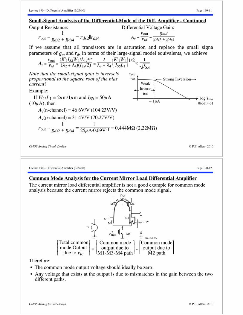
Common Mode Analysis for the Current Mirror Load Differential AmplifierThe current mirror load differential amplifier is not a good example for common modeanalysis because the current mirror rejects the common mode signal.
-
+
vic
M1 M2
M4
M5
vout ≈ 0V
VDD
VBias+
-
M3M1-M3-M4
Fig. 5.2-8A
M2
Total commonmode Output
due to vic =
Common modeoutput due to
M1-M3-M4 path -
Common modeoutput due to
M2 path
Therefore: • The common mode output voltage should ideally be zero. • Any voltage that exists at the output is due to mismatches in the gain between the two
different paths.
Lecture 190 – Differential Amplifier (3/27/10) Page 190-13
CMOS Analog Circuit Design © P.E. Allen - 2010
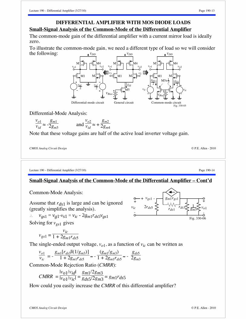
DIFFERENTIAL AMPLIFIER WITH MOS DIODE LOADSSmall-Signal Analysis of the Common-Mode of the Differential AmplifierThe common-mode gain of the differential amplifier with a current mirror load is ideallyzero.To illustrate the common-mode gain, we need a different type of load so we will considerthe following:
Differential-Mode Analysis:
vo1vid
-gm12gm3
and vo2vid
+ gm22gm4
Note that these voltage gains are half of the active load inverter voltage gain.
vic
vo1
v1
vo2
v2
VBias
ISS
VDD
M1 M2
M3 M4
M5
vo1
vid
VDD
M1 M2
M3 M4vo2 vo1
vic
vo2
VBias
ISS
VDD
M1 M2
M3 M4
2ISS M5x1
22
Differential-mode circuit Common-mode circuitGeneral circuit
2vid
2
Fig. 330-05
Lecture 190 – Differential Amplifier (3/27/10) Page 190-14
CMOS Analog Circuit Design © P.E. Allen - 2010
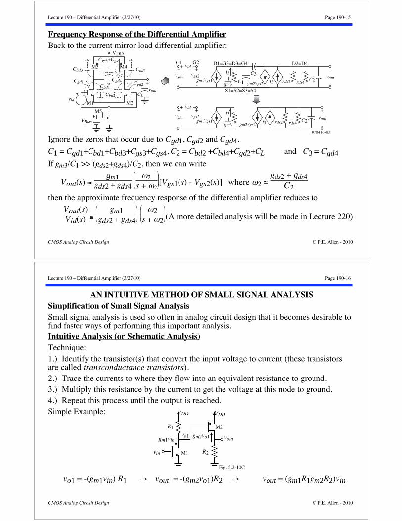
Small-Signal Analysis of the Common-Mode of the Differential Amplifier – Cont’d
Common-Mode Analysis:
Assume that rds1 is large and can be ignored(greatly simplifies the analysis).
vgs1 = vg1-vs1 = vic - 2gm1rds5vgs1
Solving for vgs1 gives
vgs1 = vic
1 + 2gm1rds5
The single-ended output voltage, vo1, as a function of vic can be written as
vo1vic
= - gm1[rds3||(1/gm3)]
1 + 2gm1rds5 -
(gm1/gm3)1 + 2gm1rds5
- gds52gm3
Common-Mode Rejection Ratio (CMRR):
CMRR = |vo1/vid||vo1/vic| =
gm1/2gm3gds5/2gm3
= gm1rds5
How could you easily increase the CMRR of this differential amplifier?
+
-vic
vgs1+ -
2rds5 rds1
gm1vgs1
rds3 gm31
+
-vo1
Fig. 330-06
Lecture 190 – Differential Amplifier (3/27/10) Page 190-15
CMOS Analog Circuit Design © P.E. Allen - 2010
Frequency Response of the Differential AmplifierBack to the current mirror load differential amplifier:
gm31gm1vgs1 rds2gm2vgs2
i3
i3
+
-
+
-
+G2
vid
vgs1 vgs2
G1
C1
-
S1=S2=S3=S4
rds4
C3C2
+
-
vout
D1=G3=D3=G4 D2=D4
M1 M2
M3 M4
VDD
M5
vout
-
+
VBias
vidCL
Cbd1
Cbd2
Cbd3 Cbd4
Cgd2Cgd1
Cgs3+Cgs4
Cgd4
gm31gm1vgs1 rds2gm2vgs2
i3
i3
+
-
+
-
+ vid
vgs1 vgs2
-
rds4C2
+
-
vout
070416-03
Ignore the zeros that occur due to Cgd1, Cgd2 and Cgd4.
C1 = Cgd1+Cbd1+Cbd3+Cgs3+Cgs4, C2 = Cbd2 +Cbd4+Cgd2+CL and C3 = Cgd4
If gm3/C1 >> (gds2+gds4)/C2, then we can write
Vout(s) gm1
gds2 + gds4 2
s + 2[Vgs1(s) - Vgs2(s)] where 2
gds2 + gds4C2
then the approximate frequency response of the differential amplifier reduces toVout(s)Vid(s)
gm1gds2 + gds4
2s + 2 (A more detailed analysis will be made in Lecture 220)
Lecture 190 – Differential Amplifier (3/27/10) Page 190-16
CMOS Analog Circuit Design © P.E. Allen - 2010
AN INTUITIVE METHOD OF SMALL SIGNAL ANALYSISSimplification of Small Signal AnalysisSmall signal analysis is used so often in analog circuit design that it becomes desirable tofind faster ways of performing this important analysis.Intuitive Analysis (or Schematic Analysis)Technique:1.) Identify the transistor(s) that convert the input voltage to current (these transistorsare called transconductance transistors).2.) Trace the currents to where they flow into an equivalent resistance to ground.3.) Multiply this resistance by the current to get the voltage at this node to ground.4.) Repeat this process until the output is reached.Simple Example:
vo1 = -(gm1vin) R1 vout = -(gm2vo1)R2 vout = (gm1R1gm2R2)vin
vin
vout
VDD
R1
gm1vin
VDD
vo1 gm2vo1
R2M1
M2
Fig. 5.2-10C
Lecture 190 – Differential Amplifier (3/27/10) Page 190-17
CMOS Analog Circuit Design © P.E. Allen - 2010
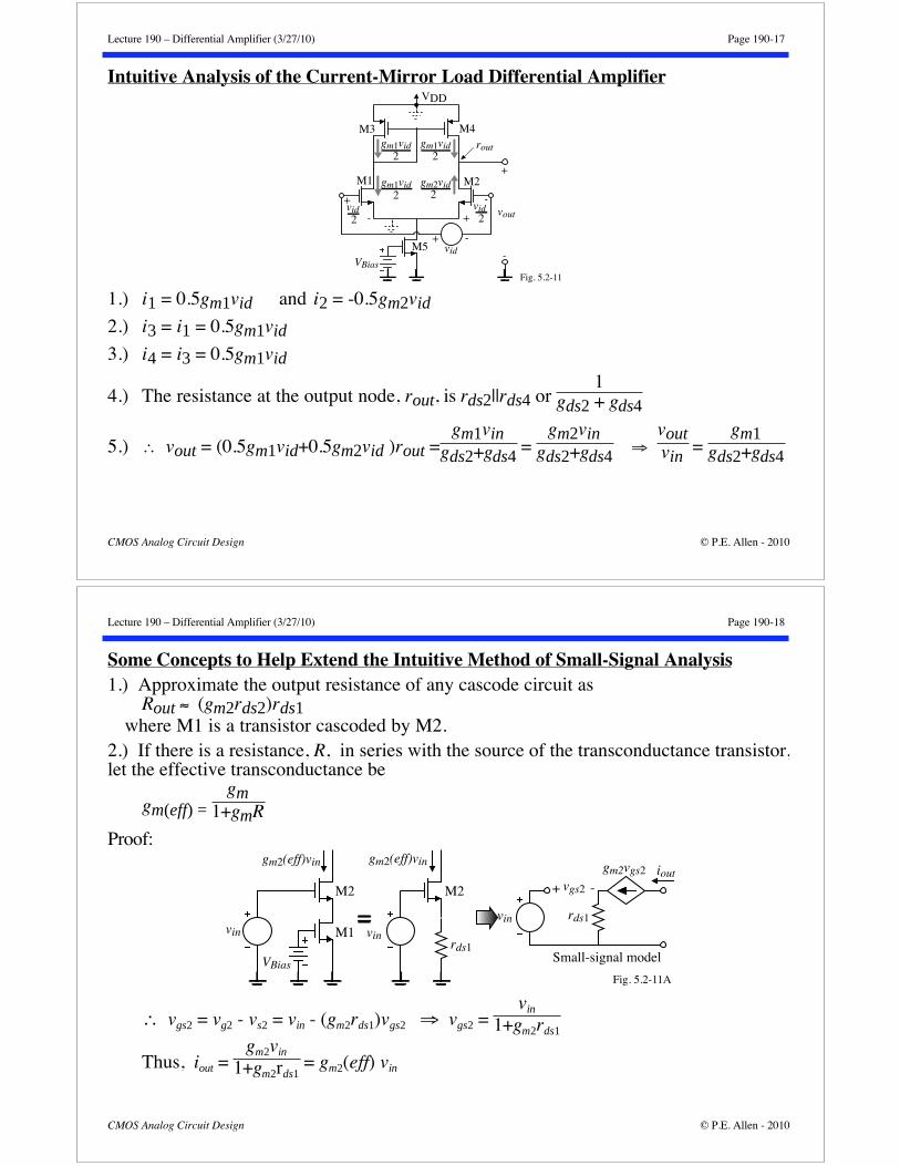
Intuitive Analysis of the Current-Mirror Load Differential Amplifier
VBias
M1 M2
M3 M4
VDD
M5
vid+
- +
-vout
gm2vid
-
+
Fig. 5.2-11
2vid2
2gm1vid
2
gm1vid2
gm1vid2
+ -vid
rout
1.) i1 = 0.5gm1vid and i2 = -0.5gm2vid
2.) i3 = i1 = 0.5gm1vid
3.) i4 = i3 = 0.5gm1vid
4.) The resistance at the output node, rout, is rds2||rds4 or 1
gds2 + gds4
5.) vout = (0.5gm1vid+0.5gm2vid )rout =gm1vin
gds2+gds4 =
gm2vingds2+gds4
voutvin
= gm1
gds2+gds4
Lecture 190 – Differential Amplifier (3/27/10) Page 190-18
CMOS Analog Circuit Design © P.E. Allen - 2010
Some Concepts to Help Extend the Intuitive Method of Small-Signal Analysis1.) Approximate the output resistance of any cascode circuit as
Rout (gm2rds2)rds1where M1 is a transistor cascoded by M2.
2.) If there is a resistance, R, in series with the source of the transconductance transistor,let the effective transconductance be
gm(eff) =
gm1+gmR
Proof:gm2(eff)vin
vin
VBias
M2
M1 vinrds1
M2
gm2(eff)vin gm2vgs2
vgs2
vin
+ -
rds1
iout
Small-signal model
Fig. 5.2-11A
vgs2 = vg2 - vs2 = vin - (gm2rds1)vgs2 vgs2 = vin
1+gm2rds1
Thus, iout = gm2vin
1+gm2rds1 = gm2(eff) vin
Lecture 190 – Differential Amplifier (3/27/10) Page 190-19
CMOS Analog Circuit Design © P.E. Allen - 2010
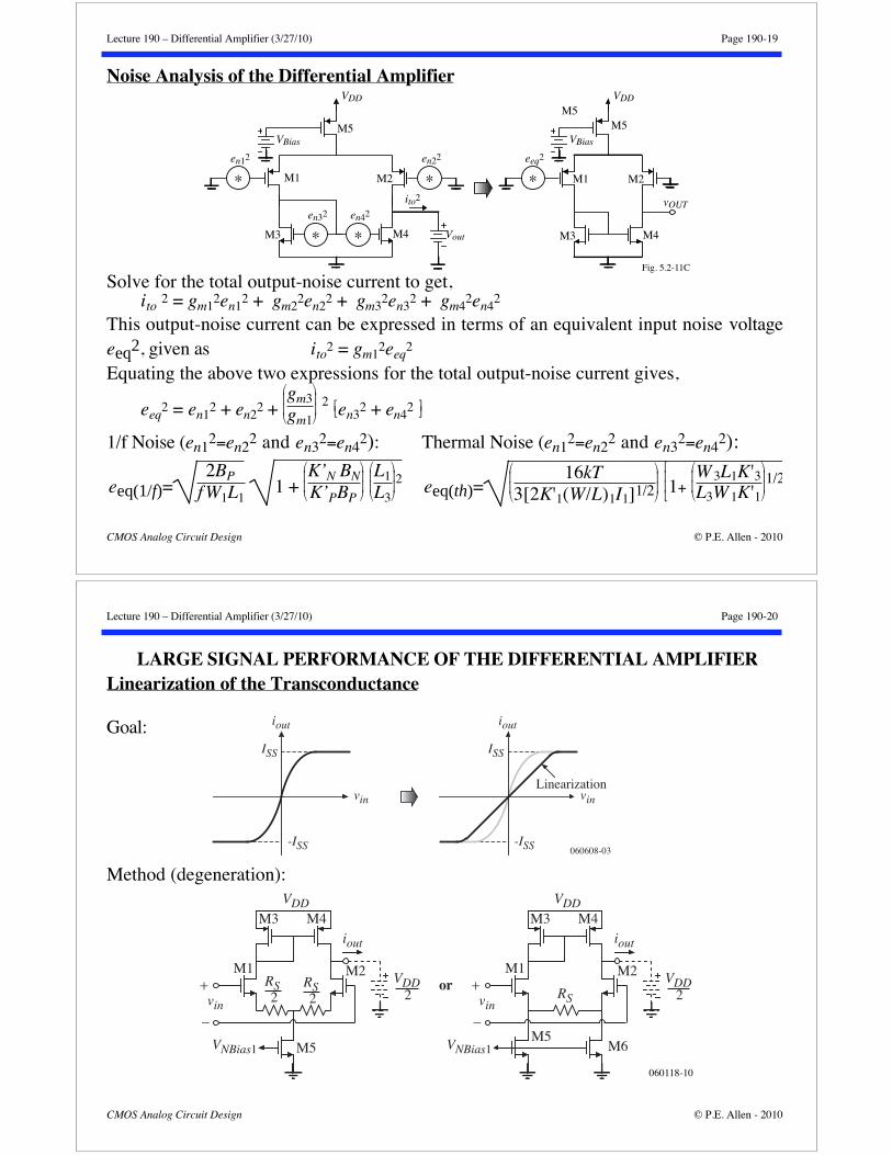
Noise Analysis of the Differential Amplifier
VBias
M1 M2
M3 M4
VDD
M5
Vout
ito2
Fig. 5.2-11C
en12
en42en32
en22 eeq2
VBias
VDD
M5
M1 M2
M3 M4
M5
vOUT
* *
* *
*
Solve for the total output-noise current to get,ito 2 = gm1
2en12 + gm2
2en22 + gm3
2en32 + gm4
2en42
This output-noise current can be expressed in terms of an equivalent input noise voltageeeq2, given as ito
2 = gm12eeq
2
Equating the above two expressions for the total output-noise current gives,
eeq2 = en1
2 + en22 +
gm3gm1
2 en32 + en4
2
1/f Noise (en12=en2
2 and en32=en4
2): Thermal Noise (en12=en2
2 and en32=en4
2):
eeq(1/f)=2BP
f W1L1 1 +
K’N BNK’PBP
L1L3
2 eeq(th)=16kT
3[2K'1(W/L)1I1]1/2 1+W 3L1K'3L3W 1K'1
1/2
Lecture 190 – Differential Amplifier (3/27/10) Page 190-20
CMOS Analog Circuit Design © P.E. Allen - 2010
iout
vin
ISS
-ISS
iout
vin
ISS
-ISS
Linearization
060608-03
LARGE SIGNAL PERFORMANCE OF THE DIFFERENTIAL AMPLIFIERLinearization of the Transconductance
Goal:
Method (degeneration):
060118-10
VDD
VDD2
iout
vin
+
−
RS2
RS2
VNBias1
M1 M2
M3 M4
M5
or
VDD
VDD2
iout
vin
+
−
RS
VNBias1
M1 M2
M3 M4
M5M6
Lecture 190 – Differential Amplifier (3/27/10) Page 190-21
CMOS Analog Circuit Design © P.E. Allen - 2010
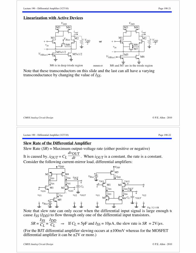
Linearization with Active Devices
060608-05
VDD
VDD2
iout
vin
+
−VNBias1
M1 M2
M3 M4
M5x1/2M5x1/2
VBias
M6
M6 is in deep triode region
or
VDD
VDD2
iout
vin
+
−VNBias1
M1 M2
M3 M4
M5M6
M6
M6 and M7 are in the triode region
M7
Note that these transconductors on this slide and the last can all have a varyingtransconductance by changing the value of ISS.
Lecture 190 – Differential Amplifier (3/27/10) Page 190-22
CMOS Analog Circuit Design © P.E. Allen - 2010
Slew Rate of the Differential AmplifierSlew Rate (SR) = Maximum output-voltage rate (either positive or negative)
It is caused by, iOUT = CL
dvOUTdt . When iOUT is a constant, the rate is a constant.
Consider the following current-mirror load, differential amplifiers:
CL
VBias
ISS
M1 M2
M3 M4
VDD
M5
vGS1+
-vGS2
+-
vG2
-
vOUT
iOUT
vG1
-
iD1 iD2
iD3 iD4
-
+
CL
VBias IDD
M1 M2
M3 M4
VDD
M5
vSG1
+
-vSG2
+
-
vG2
-
vOUT
iOUT
vG1
-
iD1 iD2
iD3 iD4
-
+
Fig. 5.2-11B
++
Note that slew rate can only occur when the differential input signal is large enough tocause ISS (IDD) to flow through only one of the differential input transistors.
SR = ISSCL
= IDDCL
If CL = 5pF and ISS = 10μA, the slew rate is SR = 2V/μs.
(For the BJT differential amplifier slewing occurs at ±100mV whereas for the MOSFETdifferential amplifier it can be ±2V or more.)
Lecture 190 – Differential Amplifier (3/27/10) Page 190-23
CMOS Analog Circuit Design © P.E. Allen - 2010
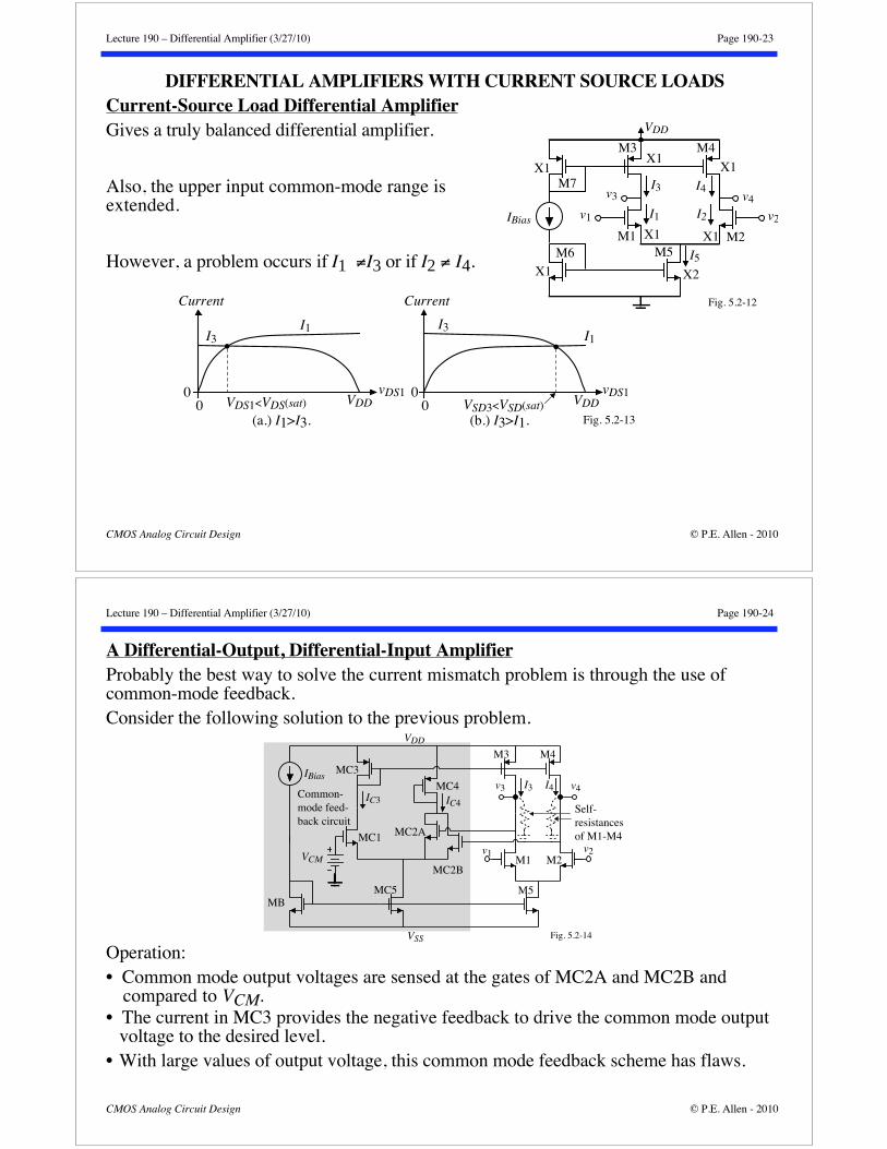
DIFFERENTIAL AMPLIFIERS WITH CURRENT SOURCE LOADSCurrent-Source Load Differential AmplifierGives a truly balanced differential amplifier.
Also, the upper input common-mode range isextended.
However, a problem occurs if I1 I3 or if I2 I4.
VDD
IBias
M1 M2
M3 M4
M5
X2
I1 I2
I3 I4
v1 v2
v3 v4
M6
M7X1
X1X1
X1
X1 X1
Fig. 5.2-12
I5
I1I3
VDS1<VDS(sat) VDD0
0
Current
I1I3
VSD3<VSD(sat) VDD0
0
Current
Fig. 5.2-13 (a.) I1>I3. (b.) I3>I1.
vDS1 vDS1
Lecture 190 – Differential Amplifier (3/27/10) Page 190-24
CMOS Analog Circuit Design © P.E. Allen - 2010
A Differential-Output, Differential-Input AmplifierProbably the best way to solve the current mismatch problem is through the use ofcommon-mode feedback.Consider the following solution to the previous problem.
v1M1 M2
M3 M4
M5
VDD
VSS
IBias
VCM
v4v3
v2
MC2A
MC2B
MC1
MC3
MC4
MC5MB
I3 I4
IC4IC3
Fig. 5.2-14
Common-mode feed-back circuit
Self-resistancesof M1-M4
Operation:• Common mode output voltages are sensed at the gates of MC2A and MC2B and
compared to VCM.• The current in MC3 provides the negative feedback to drive the common mode output
voltage to the desired level.• With large values of output voltage, this common mode feedback scheme has flaws.
Lecture 190 – Differential Amplifier (3/27/10) Page 190-25
CMOS Analog Circuit Design © P.E. Allen - 2010
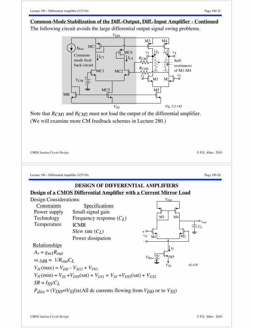
Common-Mode Stabilization of the Diff.-Output, Diff.-Input Amplifier - ContinuedThe following circuit avoids the large differential output signal swing problems.
v1M1 M2
M3 M4
M5
VDD
VSS
IBias
VCM
v4v3
v2MC2
RCM1
MC1
MC3
MC4
MC5MB
I3 I4
IC4IC3
Fig. 5.2-145
Common-mode feed-back circuit
Self-resistancesof M1-M4
RCM2
Note that RCM1 and RCM2 must not load the output of the differential amplifier.
(We will examine more CM feedback schemes in Lecture 280.)
Lecture 190 – Differential Amplifier (3/27/10) Page 190-26
CMOS Analog Circuit Design © P.E. Allen - 2010
DESIGN OF DIFFERENTIAL AMPLIFIERSDesign of a CMOS Differential Amplifier with a Current Mirror LoadDesign Considerations:
Constraints SpecificationsPower supplyTechnologyTemperature
Small-signal gainFrequency response (CL)ICMRSlew rate (CL)Power dissipation
RelationshipsAv = gm1Rout
-3dB = 1/RoutCL
VIC(max) = VDD - VSG3 + VTN1
VIC(min) = VSS +VDS5(sat) + VGS1 = VSS +VDS5(sat) + VGS2
SR = ISS/CL
Pdiss = (VDD+|VSS|)x(All dc currents flowing from VDD or to VSS)
ALA20
-
+vin M1 M2
M3 M4
M5
vout
VDD
VSS
VBias
CL
I5
Lecture 190 – Differential Amplifier (3/27/10) Page 190-27
CMOS Analog Circuit Design © P.E. Allen - 2010
Design of a CMOS Differential Amplifier with a Current Mirror Load - Continued
Schematic-wise, the design procedure is illustrated asshown:
Procedure:1.) Pick ISS to satisfy the slew rate knowing CL orthe power dissipation2.) Check to see if Rout will satisfy the frequencyresponse, if not change ISS or modify circuit
3.) Design W3/L3 (W4/L4) to satisfy the upper ICMR
4.) Design W1/L1 (W2/L2) to satisfy the gain
5.) Design W5/L5 to satisfy the lower ICMR
6.) Iterate where necessary
ALA20
-
+vin M1 M2
M3 M4
M5
vout
VDD
VSS
VBias+
-
CL
VSG4+
-
gm1Rout
Min. ICMR I5I5 = SR·CL,
ω-3dB, Pdiss
Max. ICMR
Lecture 190 – Differential Amplifier (3/27/10) Page 190-28
CMOS Analog Circuit Design © P.E. Allen - 2010
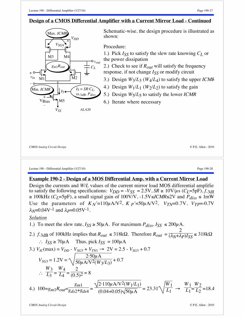
Example 190-2 - Design of a MOS Differential Amp. with a Current Mirror LoadDesign the currents and W/L values of the current mirror load MOS differential amplifierto satisfy the following specifications: VDD = -VSS = 2.5V, SR 10V/μs (CL=5pF), f-3dB
100kHz (CL=5pF), a small signal gain of 100V/V, -1.5V ICMR 2V and Pdiss 1mWUse the parameters of K N’=110μA/V2, K P’=50μA/V2, VTN=0.7V, VTP=-0.7V
N=0.04V-1 and P=0.05V-1.
Solution1.) To meet the slew rate, ISS 50μA. For maximum Pdiss, ISS 200μA.
2.) f-3dB of 100kHz implies that Rout 318k . Therefore Rout = 2
( N+ P)ISS 318k
ISS 70μA Thus, pick ISS = 100μA
3.) VIC(max) = VDD - VSG3 + VTN1 2V = 2.5 - VSG3 + 0.7
VSG3 = 1.2V = 2·50μA
50μA/V2(W3/L3) + 0.7
W3L3 =
W4L4 =
2(0.5)2 = 8
4.) 100=gm1Rout=gm1
gds2+gds4 = 2·110μA/V2(W1/L1)
(0.04+0.05) 50μA = 23.31W1L1
W1L1=
W2L2 =18.4
Lecture 190 – Differential Amplifier (3/27/10) Page 190-29
CMOS Analog Circuit Design © P.E. Allen - 2010
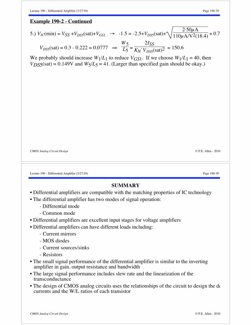
Example 190-2 - Continued
5.) VIC(min) = VSS +VDS5(sat)+VGS1 -1.5 = -2.5+VDS5(sat)+2·50μA
110μA/V2(18.4) + 0.7
VDS5(sat) = 0.3 - 0.222 = 0.0777 W5L5 =
2ISSKN’VDS5(sat)2 = 150.6
We probably should increase W1/L1 to reduce VGS1. If we choose W1/L1 = 40, thenVDS5(sat) = 0.149V and W5/L5 = 41. (Larger than specified gain should be okay.)
Lecture 190 – Differential Amplifier (3/27/10) Page 190-30
CMOS Analog Circuit Design © P.E. Allen - 2010
SUMMARY• Differential amplifiers are compatible with the matching properties of IC technology• The differential amplifier has two modes of signal operation:
- Differential mode- Common mode
• Differential amplifiers are excellent input stages for voltage amplifiers• Differential amplifiers can have different loads including:
- Current mirrors- MOS diodes- Current sources/sinks- Resistors
• The small signal performance of the differential amplifier is similar to the invertingamplifier in gain, output resistance and bandwidth
• The large signal performance includes slew rate and the linearization of thetransconductance
• The design of CMOS analog circuits uses the relationships of the circuit to design the dccurrents and the W/L ratios of each transistor