development of a microfluidic device for selective
TRANSCRIPT

DEVELOPMENT OF A MICROFLUIDIC DEVICE FOR SELECTIVE ELECTRICAL LYSIS OF PLASMA
MEMBRANES OF SINGLE CELLS
by
Duoaud Fawz Shah
A thesis submitted in conformity with the requirements for the degree of Master of Science
Medical Biophysics University of Toronto
© Copyright by Duoaud Fawz Shah 2010

ii
Development of a microfluidic device for the selective electrical
lysis of plasma membranes of single cells
Duoaud Fawz Shah
Master of Science
Medical Biophysics
University of Toronto
2010
Abstract
A primary objective of modern biology is to understand the molecular mechanisms which
underlie cellular functions and a crucial part of this task is the ability to manipulate and analyze
individual cells. As a result of interdisciplinary research, microfluidics may become the forefront
of analytical methods used by biologists. This technology can be used to gain unprecedented
opportunities for cell handling, lysis and investigation on a single cell basis. This thesis presents
the development of a microfluidic device capable of selecting individual cells and performing
selective electrical lysis of the plasma membrane, while verifying intactness of the nuclear
membrane. The device is fabricated by an improved photolithography method and integrates
molten solder as electrodes for lysis by a DC electric field. Quantification of lysis is
accomplished by video and image analysis, and measurement of the rate of ion diffusion from
the cell.

iii
Acknowledgments
The completion of this thesis has been the most significant academic challenge that I have faced;
however, overcoming the hurdles along the way would not have been possible without the
guidance, direction and support of my supervisor, Dr. Lothar Lilge. He allowed me to work
independently, and to learn from my mistakes, while always being available and accessible to
guide me through difficult times. Most importantly, I am grateful to him for helping me to
improve my thought process as a researcher. His leadership style, coupled with his overall
character has proven to me that I had the ideal supervisor for my graduate experience.
I would also like to thank the members of my supervisory committee, Dr. Jim Woodgett
and Dr. Alex Vitkin, for their support and the insight they provided to help steer my project
towards its objectives.
Sharing the challenges and victories of my work with members of the Lilge group has
made my graduate experience fulfilling and has helped me in overcoming frustration, and
sometimes coming up with inventive solutions, while keeping me grounded. For this, I would
like to thank this team of talented and extremely supportive students and staff. They provided an
environment which made it enjoyable to be at work daily, while enhancing my personal
experience as a graduate student and I wish them success in all their endeavours. Specifically, I
would like to thank Luc Charron for his advice and our many discussions which helped
overcome several fabrication challenges of the project, and Dr. Kumudesh Sritharan for helping
me with the fluorescent labelling and other in vitro work. The simulations in COMSOL would
not have been possible without the tutelage of Dr. Mohamed Abdelgawad, to whom I am
indebted. I am also grateful to Jane Walter, Benjamin Lai and Jennifer Street for their friendship
and support.
I owe the deepest gratitude to my mother for raising me to be well-rounded while
instilling the value of education. She has supported me through all my personal and academic
endeavours and has been an inspiration to me at all times. I would also like to thank my uncle
and aunt who have always encouraged me to remember my faith throughout my studies, and my
grandmother for her kindness and numerous meals which helped get me through graduate school.
Lastly, to my wonderful Daanish, I thank you for your patience, understanding and love
throughout this journey as your unwavering support has been my source of motivation.

iv
Table of Contents
Acknowledgments .......................................................................................................................... iii
List of Tables ................................................................................................................................ vii
List of Figures .............................................................................................................................. viii
List of Acronyms and Symbols ...................................................................................................... xi
Chapter 1 Introduction .................................................................................................................... 1
1 1
1.1 Overview of single cell analysis ......................................................................................... 1
1.2 Techniques for single cell analysis ..................................................................................... 6
1.2.1 Flow cytometry ....................................................................................................... 7
1.2.2 Fluorescence microscopy ........................................................................................ 8
1.2.3 Capillary electrophoresis......................................................................................... 8
1.2.4 Requirements for alternative analysis method ........................................................ 9
1.3 Single cell analysis on microfluidic platforms .................................................................... 9
1.3.1 Techniques for single cell analysis in microfluidics ............................................. 10
1.3.2 Microfluidics platform for multiple technique integration ................................... 11
1.4 Motivation for selective single cell lysis........................................................................... 12
1.5 Thesis organization ........................................................................................................... 13
Chapter 2 Electrical lysis of plasma membrane with intact nuclei ............................................... 14
2 14
2.1 Introduction ....................................................................................................................... 14
2.1.1 The plasma membrane and electroporation .......................................................... 14
2.1.2 Electrical lysis ....................................................................................................... 18
2.2 Materials and Methods ...................................................................................................... 22
2.2.1 Electric field simulations ...................................................................................... 22
2.3 Results and Discussion ..................................................................................................... 24

v
2.3.1 Electric field distribution dependency on geometry ............................................. 24
2.3.2 Electric field dependency on applied voltage ....................................................... 27
2.3.3 Determination of heat transfer to cell during lysis ................................................ 29
2.4 Conclusion ........................................................................................................................ 32
Chapter 3 Fabrication of microfluidics device with integrated electrodes for single cell lysis .... 33
3 33
3.1 Introduction ....................................................................................................................... 33
3.1.1 Design requirements of a single cell microfluidic device ..................................... 33
3.1.2 UV photolithography as a fabrication tool ............................................................ 34
3.2 Materials and Methods ...................................................................................................... 35
3.2.1 Photo mask production and optimization ............................................................. 35
3.2.2 Preparation of glass substrates .............................................................................. 38
3.2.3 SU-8 exposure and development .......................................................................... 41
3.2.4 Device fabrication by rapid prototyping of PDMS ............................................... 44
3.2.5 Material characterization of integrated electrodes ................................................ 47
3.3 Results and Discussion ..................................................................................................... 52
3.3.1 UV absorbance and micrograph resolution of photo masks ................................. 52
3.3.2 SU-8 spin coating and exposure ........................................................................... 54
3.3.3 PDMS device development ................................................................................... 57
3.3.4 Electrode material characterization ....................................................................... 60
3.3.5 Microfluidic device with integrated electrodes ..................................................... 64
3.4 Conclusion ........................................................................................................................ 65
Chapter 4 In vitro experimental verification of plasma membrane lysis ...................................... 66
4 66
4.1 Introduction ....................................................................................................................... 66
4.2 Materials and Methods ...................................................................................................... 67

vi
4.2.1 Experimental set-up .............................................................................................. 67
4.2.2 Visual monitoring of electric field induced cell lysis ........................................... 71
4.2.3 Data analysis ......................................................................................................... 72
4.3 Results and Discussion ..................................................................................................... 74
4.3.1 Flow control .......................................................................................................... 74
4.3.2 Hoechst and calcein staining and photobleaching ................................................ 74
4.3.3 Electrical lysis of 3T3 and 9L plasma membranes ............................................... 77
4.3.4 Variation of diffusion rate due to electric field ..................................................... 85
4.4 Conclusion ........................................................................................................................ 86
Chapter 5 Summary and Future Work .......................................................................................... 87
5 87
5.1 Summary ........................................................................................................................... 87
5.2 Contributions and perspectives ......................................................................................... 88
5.2.1 Microfluidic device fabrication for single cell electrical lysis .............................. 88
5.2.2 Selective electrical lysis of plasma membrane of single cells .............................. 89
5.3 Future Work ...................................................................................................................... 89
5.3.1 Engineering and fabrication aspects ..................................................................... 89
5.3.2 Integration of components .................................................................................... 90
5.3.3 Selective lysis by AC electric field ....................................................................... 92
5.3.4 Multiple fluorescent staining ................................................................................ 92

vii
List of Tables
1.1 Examples of single cell analysis techniques useful to investigate heterogeneity…….6
2.1 Dependency of simulated electric field range on applied voltage…………………....28
2.2 Calculated values of the capacitance of each dielectric layer………………………...31
3.1 Summary of printing resolution and photo films used by different suppliers………...37
3.2 Properties of electrically conductive pastes and epoxies……………………………..49
3.3 Thickness and OD measurements of 3 different photo masks…………......................53
3.4 Initial and final radiant energy per cm2 due to photo mask absorption…....................55
3.5 Variation of channel widths and gaps during fabrication process………....................60
3.6 Electrical properties of all conductive materials used as integrated electrodes……....63
4.1 Summary of diffusion rates and fluorescent intensity data for nine 3T3 cells….…….80
4.2 Summary of diffusion rates and fluorescent intensity data for nine 9L cells…............84

viii
List of Figures
1.1 Illustration of a eukaryotic cell………………………………………………………..2
1.2 The cell as a system with common input and output signals………………………….5
1.3 Integrated microfluidic device for single cell transport, lysis, capillary
electrophoresis and detection………………………………………………………....12
2.1 Illustration of phospholipid bilayer membrane……………………………………….14
2.2 Equivalent circuit representation of cell in suspension……………………………….15
2.3 Polarization of plasma membrane under influence of an electric field……………… 16
2.4 Modeled results for ΔVmem and ΔVorg, showing optimal frequency region……….......19
2.5 Illustration of various electrode configurations used in microfluidic research………..22
2.6 Geometric simulation of intended microfluidic chip including material properties......23
2.7 a) Simulation of electric field distribution between teeth-like electrodes;
b) Resistive heating between electrodes………………………………………………24
2.8 a) Simulation of electric field distribution between embedded 3-D electrodes,
with arrows shown in insulating region between electrodes and channel;
b) Resistive heating between electrodes………………………………………………26
2.9 Electric field strength as a function of distance in x-axis, showing regions of the
fluidic channel and insulating regions at an applied voltage of 4V…………………..27
2.10 Plot of electric field dependency on applied voltage as obtained from COMSOL
simulations…………………………………………………………………………….29
2.11 Parallel plate capacitor model of electrode – insulating region (C1 and C3) –
channel system (C2), showing insulating regions and channels as capacitors, with
corresponding thicknesses…………………………………………………………….30
3.1 Schematic AutoCAD drawing of integrated microfluidic device and injector
structure region………………………………………………………………………..36
3.2 Pre-printing illustration of photo mask and injector structure region………………...37
3.3 Spin speed vs. film thickness for various SU-8 photoresists…………………………40
3.4 Set-up of various layers during UV exposure of SU-8……………………………….42

ix
3.5 Illustration of cross sectional view of a microfluidic channel and method of
measuring side wall angle…………………………………………………………….44
3.6 Illustration of multi-step soft lithography processs…………………………………...45
3.7 Corona treater with PDMS chip and spin coated cover glass on a motorized
stage…………………………………………………………………………………...47
3.8 a) Tubing filled to measure resistance b) Cross sectional view and c) top view
of chip with electrode filled; d) Cross sectional view of chip showing resistance
measurement with inserted copper wire………………………………………………50
3.9 a) Absorbance as a function of wavelength for printed parts of photo mask,
b) Absorbance as a function of wavelength for transparent part of each photo mask...52
3.10 Micrograph images of mask features from 3 suppliers………………………………..54
3.11 Resolution improvement of SU-8 structures using glycerine for different
exposure times…………………………………………………………………………56
3.12 Micrograph images of PDMS channels showing side wall angle improvement
with glycerine at an exposure time of 12.5s…………………………………………...57
3.13 Side wall angle as a function of channel width for different exposure times…………57
3.14 (a) Central plane in the x-axis; (b) Central plane showing z-axis view (top),
and y-axis view through the fluidic channel (right); (c) Sample profiles through
various regions…………………………………………………………………………59
3.15 Physical properties of integrated electrodes made of different material, with
(a) carbon-PDMS; (b) nickel paste; (c) silver paste……………………………….…..61
3.16 Resistance as a function of tubing length for electrode materials………………….….62
3.17 Final microfluidic device with integrated solder electrodes……………………….….64
4.1 Image of flow control system……………………………………………………….....68
4.2 Calcein AM molecule (C46H46N2O23) and excitation/emission spectra…………….....69
4.3 Hoechst 333342 molecule (C27H37Cl3N6O4) and excitation/emission spectra…….…..70
4.4 Circuit diagram of function generator with external DC offset…………………….....71
4.5 Illustration of direction of fluorescent profile analysis………………………………..73
4.6 a) Hoechst staining of nuclei in cell reservoir; b) Single cell Hoechst stain
depicting line along which fluorescent intensity profile………………………………74
4.7 a) Hoechst fluorescent intensity profile as a function of position for various time
points; b) Area under each intensity peak as a function of time………………………75

x
4.8 Calcein staining of cytoplasm in cell reservoir; b) Single cell calcein stain
depicting line along which fluorescent intensity profile………………………………76
4.9 a) Calcein fluorescent intensity profile as a function of position for various time
points; b) Area under each intensity peak as a function of time……………………....76
4.10 a) Fluorescent image of cytoplasm, a) before lysis, 0s; b) after lysis, 4s……………..77
4.11 Fluorescent intensity profile as a function of position for 3 different 3T3 cells
on the same chip, a) cytoplasmic changes over time; b) nucleic changes between
t = 0s and t = 6s………………………………………………………………………..78
4.12 Plot of FWHM vs. Time, showing diffusion region and start of electric field
application……………………………………………………………………………..79
4.13 Fluorescent intensity profile as a function of position for 3 different 9L cells on
the same chip, a) cytoplasmic changes over time; b) nucleic changes between
t = 0s and t = 6s………………………………………………………………………..82
4.14 Plot of FWHM vs. Time, showing diffusion region and start of electric field
application……………………………………………………………………………..83
4.15 Dependency of diffusion rate of calcein on mean electric field strength for 3T3 cells..85
5.1 Parallelized system with multiple electrode filling ports……………………………...91
5.2 (a) Staining of nucleus with Hoechst and mitochondria with Mitotracker Red;
(b) Triple staining of cytoplasm (Calcein AM), nucleus (Hoechst) and plasma
membrane (R18)……………………………………………………………………….92

xi
List of Acronyms and Symbols
Acronyms
2-D 2 dimensional
3-D 3 dimensional
AC Alternating current
Bn Bismuth
CAD Computer-aided design
DC Direct current
DPI Dots per inch
fps Frames per second
FWHM Full width at half maximum
GFP Green fluorescent protein
GaIn Gallium-Indim
H2SO4 Sulphuric acid
H2O2 Hydrogen peroxide
In Indium
ITO Indium tin oxide
LIF Laser induced fluorescence
MEM Minimum essential medium
MEMS Microelectromechanical systems
OD Optical density
PDMS Polydimethylsiloxane
PMMA Polymethylmethacrylate
rad Radians
RPM Revolutions per minute
RTV Room temperature vulcanization
Sn Tin
USA United States of America
UV Ultraviolet

xii
V:V Volume to volume
VEGF Vascular endothelial growth factor
Symbols
ERAD Radiant energy [mJ]
P Lamp power [mW]
texp Exposure time [s]
ρ Electrical resistivity [Ω·cm]
σ Electrical conductivity [S·m-1
]
R Resistance [Ω]
A Surface area [m2]
l Length [m]
AOD Optical density [dimensionless]
I Radiant intensity [mW·cm-2
]
I0 Initial radiant intensity [mW·cm-2
]
u Fresnel number [dimensionless]
x Slit width [µm]
λ Wavelength [µm]
υ Side wall angle [0]
y Vertical distance between mask and substrate [µm]
RE Resistance of extracellular medium [Ω]
CE Capacitance of extracellular medium [F]
RC Resistance of cytoplasm [Ω]
CM Capacitance of cell membrane [F]
E Electric field [V·m-1
]
r Radius [m]
θ Polar angle [0]
t Time/pulse duration of the electric field [s]
f Frequency [Hz]
τc Charging time constant [s-1
]

xiii
Continued
εr Relative permittivity [dimensionless]
ε0 Permittivity of free space [F·m-1
]
Vapp Applied voltage [V]
d Distance of separation [m]
C Capacitance [F]
CT Total capacitance [F]
W Work [J]
m Mass [kg]
c Specific heat capacity [J·kg-1
·K-1
]
ΔT Change in temperature [K]
I Current [A]
Ec Dissipated energy [J]
1
Chapter 1 Introduction
1.1 Overview of single cell analysis
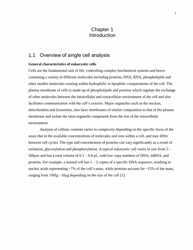
General characteristics of eukaryotic cells
Cells are the fundamental unit of life, controlling complex biochemical systems and hence
containing a variety of different molecules including proteins, DNA, RNA, phospholipids and
other smaller molecules existing within hydrophilic or lipophilic compartments of the cell. The
plasma membrane of cells is made up of phospholipids and proteins which regulate the exchange
of other molecules between the intracellular and extracellular environment of the cell and also
facilitates communication with the cell‟s exterior. Major organelles such as the nucleus,
mitochondria and lysozomes, also have membranes of similar composition to that of the plasma
membrane and isolate the intra-organelle compounds from the rest of the intracellular
environment.
Analysis of cellular contents varies in complexity depending on the specific focus of the
assay due to the available concentrations of molecules and ions within a cell, and may differ
between cell cycles. The type and concentration of proteins can vary significantly as a result of
oxidation, glycosylation and phosphorylation. A typical eukaryotic cell varies in size from 5 -
500µm and has a total volume of 0.1 – 0.8 pL, with low copy numbers of DNA, mRNA, and
proteins. For example, a normal cell has 1 – 2 copies of a specific DNA sequence, resulting in
nucleic acids representing ~7% of the cell‟s mass, while proteins account for ~15% of the mass,
ranging from 100fg - 10µg depending on the size of the cell [1].
2
Figure 1.1: Illustration of a eukaryotic cell (Adapted from [2])
Importance of single cell analysis
The ability to detect, identify, quantify and structurally analyze biomolecules of a particular type
from a large population of cells has led to a wealth of knowledge in molecular and cell biology,
which has culminated in the completion of the human genome sequence and that of hundreds of
other species. Well established protocols for gel electrophoresis, western, southern and northern
blotting, have enabled the separation of proteins, DNA and RNA respectively. In addition, X-ray
crystallography and NMR methods have solved the structures of complex biomolecules at atomic
resolution [3], mass spectrometry has identified and quantified a wide range of proteins, lipids
and metabolites [4], while microarrays probe large numbers of genes and proteins. These
methods and protocols collect a large volume of high-quality data based on population analysis.
While the techniques described above used by molecular biologists have yielded a wealth
of information on the properties of molecules, a systems biologist using those techniques would
be substantially data-starved due to a lack of information on the context in which molecules
operate and other biochemical processes which occur on short timescales or non-synchronously.

3
This includes, but is not limited to, enzyme – substrate relationships, physical interactions and
gene regulatory networks and their dynamic changes. A challenging, yet informative solution to
these dilemmas is comprehensive and quantitative analysis at the single cell level. The challenge
lies in detection, isolation, transport and in most instances, lysis of the cell of interest, while
highly sensitive analytical techniques are required since the amount of analyte present in or
extracted from a single cell is minute. Meanwhile, single cell measurements are informative
since a unique set of data is obtained for each cell and can be compared to or combined with data
from other individual cells to compute the distribution of the measured value over a population
of cells. Conversely, classical methods such as flow cytometry yield data that is averaged over a
large number of cells in each assay.
Cells can be classified at a significantly improved resolution by gaining knowledge of the
distribution and statistical significance of values over a population of individual cells, which
permits the detection of cellular variabilities, and for the discrimination between stochastic and
deterministic events within a cell. The ability to carry out extensive and robust measurements on
single cells offers the opportunity to further advance the knowledge and understanding of
cellular functions for the purpose of biology and medicine.
Heterogeneity of single cells and proteomics
Cellular heterogeneity is evident among individual cells that may be identical in appearance and
even those born from the same parent cell, as shown by Hu et al [5], as they differ in numerous
characteristics which include gene and protein expression, concentration of critical metabolite or
ion, and patterning cellular response to stimuli.
In proteomics, the spatial and temporal location of a protein is required to explain its
function; however, a cell responding to its environment, passing through cell cycles or recycling
its content results in synthesis, modification and degradation of proteins. Consequently, not all
proteins are present in all cells, with many having a fleeting existence. Di Carlo and Lee [6]
eloquently explain cellular heterogeneity by considering protein expressions from a bimodal
distribution of a specific cell line with high and low copy numbers of a specific protein. Classical
ensemble protocols would mask the bimodal distribution within the cell ensemble by detecting
only a mean value across all cells, while analysis of individual cells could resolve two distinct
subpopulations – one with high and another with low copy numbers – thus revealing two
different states of expression levels. The same is true, regardless of what is being assayed,

4
whether it be mRNA or other small molecules. While an assessment of expression levels do not
necessarily address function directly, the knowledge of when and where a gene is expressed can
provide information regarding the potential roles of these genes and possibly lead to gene
discovery in other species [7].
In the realm of stem cell research, recognizing heterogeneity and being able to monitor
the proteome on a cell by cell basis would yield greater understanding of the steps involved in
development. As pluripotent stem cells progress first to precursor cells then into differentiated
progeny cells, their protein expression level changes as is similarly observed when an embryo
changes from a zygote into a fully developed individual [1].
By hierarchical processes of proliferation and differentiation, stem cells are able to
generate large numbers of mature cells, while the stem cell pool itself is continuously self-
renewed. These developmental processes exist in many adult tissues, including colon, skin, blood
and brain. The hypothesis of the cancer stem cell suggests that the balance between
differentiation and self-renewal becomes deregulated while the basic hierarchical structure
remains [5, 8]. Evidence of cellular heterogeneity in populations at various stages of
differentiation exists in tumours and biopsies have shown that the majority of cells within the
tumour may be normal, while within the sub-population of abnormal cells significant
heterogeneity exists. It is further hypothesized that cell to cell heterogeneity in protein expression
and cellular composition of a tumour increases as the disease progresses and can thus be
correlated with prognosis [9].
Neuroscience offers another example of heterogeneity, where individual neurons in the
central nervous system reflect differences in their contents and architecture [10], making the
brain the most complex organ in all vertebrates. Classification of these differences offers the
opportunity to better understand the function of each cell and the biological neural network.
Single cells as individual systems
Cell biology seeks to identify how the collection of environmental stimuli to which a cell is
exposed may influence the behaviour of that cell. By considering the cell to be a system,
processing time-dependent input signals into output responses (Fig. 1.2), and being able to
predict this relationship, can result in an understanding of higher level organization of tissues,
organs and organisms, which may aid in determining therapeutic approaches to correct flaws
within the organization. An example of this is the cellular microenvironment or „niche‟, which

5
stem cell differentiation and self-renewal are dependent upon. Additionally, extracellular signals
influence programmed cell division and apoptosis on which normal form and structure of
organisms rely. These environmental factors include chemical signals, biological signals, and
physical signals inclusive of electrical, mechanical and thermal factors.
Figure 1.2: The cell as a system with common input and output signals (Adapted from [11])
It would be expected that with knowledge of the ensemble of environmental stimuli, a
prediction of the expected behaviour of a particular cell could be made; however, cells under
apparently identical environmental conditions have displayed heterogeneity [12], attributed
partly to probabilistic behaviour in the decision making process connecting input and output
signals. Because of the heterogeneity within a population, researchers seek tools that afford the
ability to analyze a quantity of single cells exposed to controlled input signals to determine the
variance in responses. Furthermore, this requires the analysis of as many analytes as possible
from each cell to understand the variety of internal processes that may have occurred, leading to
the observed responses, and the spatial and temporal location of the analytes.

6
1.2 Techniques for single cell analysis
A multitude of technologies now exist for the analysis of variations in chemical constituents in
single cells within a population. The tool chosen is typically dependent upon the analyte of
interest, the number of analytes to be detected, mechanism of detection and the influence of the
analytical tool by interference or modification of cellular constituents. Table 1.1 summarizes
some techniques used to investigate heterogeneity in single cells, and is followed by a brief
description of three of the more common methods.
Technique Single cell measurement Cell types investigated
Flow cytometry Noise in abundances of GFP- fusion
proteins
Yeast
Fluorescence
microscopy
Intracellular calcium release to
identify subpopulations differing in a
particular receptor
Human osteoblasts
CE – biomolecules Two dimensional separation of
proteins that are fluorescently
labelled on-line
MC3T3-E1 osteoprogenitor
and MCF-7 breast cancer cells
CE – organelles Separation and detection of
mitochondria labelled with DsRed2
143B osteosarcoma cells
Optical well arrays Kinetics of various gene expression
using GFP reporter
Escherichia coli
Electrochemical
detection
Time profile of bursts of insulin
secretion
Rat and human pancreatic beta
cells
Raman
microspectroscopy
Changes in Raman spectra indication
coexisting cell types
Clostridium beijerinckii in an
acetone-butanol fermentation
reactor
7
MALDI-MS Identification of neuropeptides Neuron cells isolated from
Aplysia californica
LCM and cDNA
microarray analysis
Gene expression profiling pointing
to two subpopulations
CA1 neurons from rat
hypocampus
Mulitplexed, real-time
RT-PCR
Quantification of 20 different
mRNAs
Human small intestine cells
GFP: Green fluorescent protein; CE: Capillary electrophoresis; MALDI-MS: matrix assisted laser
desorption/ionization mass spectrometry; LCM: laser capture microdissection; RT-PCR: reverse transcriptase
polymerase chain reaction
Table 1.1: Examples of single cell analysis techniques useful to investigate heterogeneity and the cell systems
investigated by various researchers (Adapted from [13])
1.2.1 Flow cytometry
Flow cytometry is a technique based on the principles of light scattering, light excitation and
emission of fluorescence. Cells or particles, ranging in sizes from 0.2 - 150µm, are passed in
single file by hydrodynamic focusing through a laser beam for sequential illumination. Scattering
parameters yield morphological information and can either be based on forward scatter, which is
dependent on cell volume, or side scatter, which correlates to inner complexities such as
membrane roughness, shape of the nucleus and cytoplasmic content. Meanwhile, depending on
the target, fluorescence provides functional and structural information, while affording the ability
to count, and select sub-populations of cells by fluorescence-activated cell sorting. Flow
cytometry analyses tens of thousands of cells per second and the information obtained allows a
statistical analysis of the population based on each cell or particle. Although flow cytometry
offers extremely high throughput and analysis of parameters such as total DNA or RNA content,
enzymatic activity, pH, cell viability and a long and constantly expanding list of other
parameters, it is limited due to its physical configuration, making it difficult to couple with the
subsequent steps for chemical cytometry [14]. Furthermore, cells remain in suspension for long
periods prior to detection, disrupting the biochemical balance between neighbouring cells, which
may alter cellular processes such as transcription and translation.

8
1.2.2 Fluorescence microscopy
Fluorescence microscopy is the quintessential imaging technique used in cellular and molecular
biology because of its intrinsic selectivity and specific detection of molecules at small
concentrations with good signal-to-background ratio. More than 3000 fluorescent probes exist to
label virtually any imaginable aspect of a biological system, while the large spectral range of
fluorophores allows simultaneous imaging of different cellular, subcellular and molecular
component [15]. This technique allows protein and gene expression to be measured as a function
of spatial position within a sample, yielding expression gradients, for example, for various types
of VEGF [16]. Additionally, the development of genetically encoded fluorophores, particularly
GFP and its variants, has allowed protein components of living systems to be genetically tagged,
making it possible to study protein-protein interactions and monitoring signalling events in living
cells [17]. The major caveat of fluorescence microscopy is its very low throughput and limitation
to a small number of fluorescence colours (N ~ 3), even when using advanced microscopy
techniques such as confocal and two-photon; however, this problem can be overcome with the
integration of hyperspectral imaging techniques [18]. Like flow cytometry, this technique is
constrained by the requirement of having apriori knowledge of the genes or proteins of interest,
and the availability of a suitable fluorophore.
1.2.3 Capillary electrophoresis
Capillary electrophoresis is the conventional tool used to perform high efficiency differential
transportation and separation of large and small molecules from single cells based on the
molecule‟s size, charge and hydrophobicity. The technique employs narrow bore capillaries (2-
200 µm inner diameter) in which separations are facilitated by the use of high voltages,
generating electroosmotic and electrophoretic flow of conductive buffer solutions and ionic
species respectively. Separation properties and the resultant electropherogram have characteristic
similarities to traditional polyacrylamide gel electrophoresis (PAGE) and modern high
performance liquid chromatography (HPLC) [19]. Capillary electrophoresis has the ability to
analyze the contents of single cells when capillaries of small inner diameters (2-10µm) are used,
allowing injection volumes in the pico and possibly femtoliter range. Furthermore, as first
demonstrated by Huang et al [20], the development of capillary array electrophoresis has given
rise to increased throughput by this technique while coupled capillaries with different separation

9
properties enable 2-D analysis of protein contents from single cells [21]. Unfortunately, run
times for high resolution separation can reach hours, thus reducing the throughput even if an
array of capillaries is used.
1.2.4 Requirements for alternative analysis method
The shortcomings identified above highlight the need for an analytical tool that has the ability to
address the following issues:
• selection of a priori identified cells from an ensemble,
• permit subcellular localization,
• increase the number of analytes from a single cell,
• enable high throughput to generate population statistics.
1.3 Single cell analysis on microfluidic platforms
The need for an ideal analytical tool capable of investigating a large number of parameters from
each cell within a population to identify variation, while concurrently having high throughput to
allow significant statistical analysis, has led to greater research efforts in the realm of
microfluidics.
Microfluidics, or lab-on-a-chip, is the technology of controlling and manipulating fluids
on the order of picolitres to microlitres using microchannels that are between 1-500µm in size.
Consequently, because of their small size and small volume, these devices are ideal for the
confinement and subsequent analysis of either whole or lysed single cells, making novel
experimentation a possibility while providing sophisticated and well controlled environments for
cellular investigation.
Devices are fabricated using MEMS techniques, mimicking well-defined processes in the
microelectronics industry and have typically been developed in glass and quartz, whose
transparent properties are ideal for optical analysis. However, polymers have become the
materials of choice for biological experimentation in the last 5 years [22]. Because a significant
number of devices are fabricated to meet a particular requirement, a plethora of additional
features have been integrated within the microfluidic environment to enable selection,

10
confinement, and lysis, of single cells. Examples of these include pumps and valves [23], optical
tweezers [24], dielectrophoretic traps [25], microdroplets [26], and electrodes [27, 28].
The success of this technology is based upon its enhanced analytical performance,
allowing fast, highly sensitive and reproducible analysis, while requiring low consumption of
chemicals and energy, thus making it less expensive at shorter processing times [22]. The ability
to perform parallel analysis or successive operations on the same device, sample manipulation,
reduced loss of analytes and contamination, and the possibility of high throughput is making
microfluidics a popular avenue to investigate cellular heterogeneity. Many of the traditional
techniques, discussed in Sections 1.2.1-1.2.3, have also been translated onto microfluidic devices
and will be described briefly.
1.3.1 Techniques for single cell analysis in microfluidics
Flow cytometry
The emergence of optofluidics, where microfluidics and photonics merge, has allowed the
integration of polymer waveguides and lenses for the purposes of excitation, focusing and
detection of light within the microchip, significantly alleviating the problems posed by micro-
macro interfacing as well as the interface with the user. As a result, numerous variations of
microchip based flow cytometers have been developed for sorting and analysis of single cells
and particles, ranging in size from 1-20µm [29, 30]. While the laminar flow conditions within
microfluidic systems reduces perturbations to cell physiology during sorting of viable cells,
microflow cytometers, with sorting speeds up to 500 particles·s-1
[30], have yet to match
conventional systems in performance.
Fluorescence microscopy
The same principles of fluorescence microscopy in macro devices for single cell analysis,
described in Section 1.2.2, apply within microfluidic systems. However, while microfluidic
systems have achieved high levels of integration with pumps and valves, electrodes and
waveguides, after sample preparation and processing within the microfluidic device, there is still
a need for fluorescence imaging and detection. Consequently, off-chip bulk optical elements

11
such as lenses and microscopes are common requirements for fluorescent microscopy in
microfluidics [24].
Capillary electrophoresis
Due to the narrow fluidic channels and confinement available in microfluidic devices, capillary
electrophoresis has been one of the most successfully translated and widely used macro
technologies on a microfluidic platform. The small chemical and energy footprints coupled with
the ability to fabricate parallel channels, allowing simultaneous separation and high throughput,
are desired features for researchers. Additionally, the electric field required to enable efficient
separation and electroosmotic flow can be achieved in microfluidic devices by using
significantly lower applied voltages as the length of the separation channels are shorter [31],
which also enable faster separation and shorter run times. The major limitation of capillary
electrophoresis in microfluidics is the detection of analytes, specifically when parallel separation
channels are used. Traditionally, a fluorescence microscope has been sufficient to detect analytes
in up to 8 parallel channels [24]; however more sensitive optical detection systems using
cylindrical optics have resulted in better sensitivity in detecting smaller molecules [32].
1.3.2 Microfluidics platform for multiple technique integration
Microfluidic technology offers an effective method of integrating multiple components to select,
manipulate, lyse and analyse single cells within a confined and well controlled fluidic
environment. Many of the macro techniques used for single cell analysis have been translated to
microfluidic platforms with comparable or better results. The overall aim of this program is to
develop a functional microfluidic device capable of selecting single cells from a population of
cells using optical tweezers [24], load individual cells into parallel channels, perform selective
lysis of the plasma membrane and other intracellular organelles, and use capillary electrophoresis
to separate the components of different fractions of the cell in sequential analytic steps while
using a high numerical aperture fiber-optic array for multiple single point detection (Fig. 1.3).
This thesis will be focused on developing a microfluidic device with integrated electrodes to
perform selective electrical lysis of the plasma membrane while demonstrating intactness of the
nuclear membrane, which is to be ruptured in a subsequent step.

12
Figure 1.3: Integrated microfluidic device for single cell transport, lysis, capillary electrophoresis and detection
(Courtesy of Luc Charron)
1.4 Motivation for selective single cell lysis
Currently, even on a microfluidic platform, single cell analytical techniques are unable to
separate the analysis of the various compartments of the cell, thus sequential lysis can be a low
resolution alternative to on chip microscopy. As a result of whole cell lysis, protein expressions
can only be measured for the entire single cell, whereas for signalling studies, the challenge is to
distinctly identify from what organelle within a cell a particular protein or molecule originated.
Gaining the ability to spatially and temporally determine the translocation of proteins and
molecules between cellular compartments can significantly increase the wealth of knowledge on
cellular functions, specifically understanding signalling pathways and the effects of
environmental factors on these pathways and cellular response. The main caveat of single cell
analysis is that it is impossible to repeat experiments on that particular cell, but with the ability to
perform analysis on different parts of the cell separately, the potential exists to increase the
information content from a single cell while using only a single fluorescent probe, quantifying a
protein of interest expressed at various sites or in various compartments.
Lysis regions

13
1.5 Thesis organization
This thesis presents an argument in support of single cell analysis to investigate heterogeneity
among cells and the use of microfluidics as a tool to perform analysis. In Chapter 2, a discussion
of the advantages of electrical lysis, the physical mechanisms involved in this process, and a
numerical model of the anticipated electric field is presented. The aim is to determine the applied
voltage required to induce lysis while quantifying the thermal effects of such a process on the
cell of interest. Chapter 3 details the fabrication and optimization of a microfluidic device and
the integration of electrodes. Chapter 4 describes the in vitro experiments performed to
demonstrate selective lysis of the plasma membrane. Finally, Chapter 5 concludes with a
summary of each chapter, highlighting the main findings in each, as well as outlining potential
future research.

14
Chapter 2 Electrical lysis of plasma membrane with intact nuclei
2.1 Introduction
2.1.1 The plasma membrane and electroporation
Plasma membrane
The phospholipid bilayer membrane, or plasma membrane, of a cell comprises an aqueous
solution, sandwiched by two fatty acid monolayers which are polar and hydrophilic (Fig. 2.1).
The inherently high electrical resistance (~104Ω [33]) of the membrane, results in it acting as a
dielectric barrier between the conductive intracellular, and extracellular aqueous environments,
which differ in osmolarity and ionic concentration. Consequently, a resting potential, typically
ranging from 60mV to 110mV [34, 35], exists across the plasma membrane and the system is
commonly modeled as a parallel plate capacitor [33, 36], with the membrane as a dielectric (Fig.
2.2)
Figure 2.1: Illustration of phospholipid bilayer membrane (Adapted from [37])

15
Figure 2.2: Equivalent circuit representation of cell in suspension (Adapted from [33])
Electroporation
In the presence of an external electric field, the membrane is polarized and dipoles are formed
either within or at the interfaces of the membrane and aqueous environments, inducing a
transmembrane potential, ΔVm, which leads to electroporation. This process relies on the weak
nature of the hydrophobic-hydrophilic interactions in the phospholipid bilayer. Several
theoretical models exist to explain the process of electroporation; however, the most commonly
used is the transient aqueous pore mechanism hypothesis proposed by Weaver et al [38] and
expanded by others [35, 39], in which a pulsed external electric field rapidly rearranges the
localized structures, polarizing the membrane and increasing its electrical conductivity while
inducing thermal fluctuations. As a result, hydrophobic pores appear randomly on the surface of
the membrane, and transition under the stress of the transmembrane potential, becoming aqueous
pathways, or reversible hydrophilic pores, typically at a threshold ΔVmem of 0.5-1.2V. For a
spherical cell, assumed to have a membrane that is a pure dielectric, ΔVmem, can be obtained by
Equation 2.1 when under the influence of a DC field, and Equation 2.2 for an AC field [35, 40].
Where:
RE – Resistance of extracellular medium
[Ω]
CE – Capacitance of extracellular
medium [F]
RC – Resistance of cytoplasm [Ω]
CM – Capacitance of cell membrane [F]

16
(
)
(
)
√
(
⁄ )
Where:
E is the value of the electric field in the extracellular environment [V·m-1
],
r is the radius of the cell [m],
θ is the polar angle measured between the centre of the cell and the direction of the electric
field [0],
t is the time/pulse duration of the electric field [s],
f is the frequency of the applied AC field [Hz],
τc is the charging time constant of the plasma membrane [s-1
],
Cmem is the capacitance of the plasma membrane per unit area [F],
ρi is the electrical resistivity of the intracellular environment, particularly the cytoplasm
[Ω·m],
ρe is the electrical resistivity of the extracellular environment [Ω·m],
Figure 2.3: Polarization of plasma membrane under the influence of an electric field

17
The expression for the time constant, τc, is obtained by modelling the system as a parallel plate
capacitor (Fig. 2.2) surrounded by two layers of extracellular environment. Based on accepted
values for Cmem, ρi, and ρe [33, 41], τc is usually ~ 100ns, thus in cases where the pulse duration
is much greater than the charging time of the plasma membrane (t >> τc), Equations 2.1 and 2.2
can be reduced to Equations 2.4 and 2.5 respectively.
√
An extension of this theory, following Equations 2.4 and 2.5, suggests that intracellular
organelles, such as the nucleus and mitochondria, have a unique transorganelle membrane
potential, which can be exploited to permit electroporation of organelles, without affecting the
integrity of the plasma membrane [28]. This is due entirely to their smaller radii when
considering a DC field, while the radii, membrane capacitance and charging time constant are
important factors when an AC field is applied. Under the influence of an AC field, selective
electroporation of intracellular organelles is only possible using ultrashort pulse durations (~ns),
which prevent the charging time of the plasma membrane to be reached (t < τc), coupled with
very high applied voltages to create a larger electric field across the cell. Equation 2.6 and 2.7 are
modifications of 2.4 and 2.5 respectively, and determines the transorganelle membrane potential,
where subscripts org represents within or of the organelle, and int, represents intracellular.
√ ( )
(
⁄ )

18
Applications of electroporation
Common applications of electroporation are focused on the creation of a few holes at the cells
equator, relative to the electric field (θ = 00), to enable transport into the cell. Whereas pores on
the plasma membrane are rendered open in microseconds, resealing of the pores occurs over a
range of a few minutes and during these times, foreign molecules, DNA and drugs, among
others, can be introduced to the target cell. The most common use of electroporation is DNA
transfection whereby a specific gene is introduced to the host cell via a plasmid in order to
investigate a particular function or structure. Similarly, plasmids can be transferred between cells
incubated together to exchange desirable features when pores are open. Clinically, due to the
stability of DNA, vectors containing genes can be delivered during gene therapy to treat a
genetic disorder or to replace a defective gene. Prausnitz et al [42] showed that electroporation
can be effective in transdermal drug delivery by forming pores in the stratum corneum – the
outermost layer of epidermis, which then allow drugs to reach a target tissue. This method has
also been extended to cancer tumour electrochemotherapy where disruption of the tumour cell
membrane increases the amount of drug than can be delivered.
2.1.2 Electrical lysis
Selective lysis by direct and alternating current sources
The work in this thesis extends the mechanism of reversible electroporation, in which membrane
pores are re-sealable, to a regime of irreversible electroporation, where pores become too large to
be re-sealed, referred to as electrical lysis. The plasma membrane is permanently ruptured when
an applied voltage creates an external electric field across the membrane, inducing a
transmembrane potential in excess of the threshold value, ΔVmem. By exploiting the differences
in size and electrical properties mentioned above, a specific electrical pulse can lyse the plasma
membrane with minimal impact on intracellular organelles.
An electric field produced by a direct current (DC) source is the simplest and most
obvious choice for selective lysis, since the subcellular organelles would experience no
transorganelle membrane potential, while the plasma membrane experiences a large
transmembrane potential. However, while DC sources have been used predominantly for cell
lysis, specifically in microfluidic devices for single cell lysis [24, 43, 44], the generation of a
large, continuous electric field requires the application of a high applied voltage. As a result, the

19
water electrolysis threshold (~ 1V) is usually exceeded, leading to the formation of bubbles and a
change in pH near the electrodes which may interfere with subsequent sampling processes. Using
an alternating current (AC) source to generate the electric field would minimize the effects of
water hydrolysis; however, Lu et al [28] have shown that an optimal frequency, in the range 1-
100 kHz (Fig. 2.4), must be reached to be able to perform selective lysis. Consequently, to avoid
the negative effects of using a DC source, and the requirement to find an optimal frequency with
an AC source, a pulsed DC source will be used in this project.
Figure 2.4: Modeled results for ΔVmem and ΔVorg, showing optimal frequency region (Adapted from [28])
Comparison of lysis techniques
Several alternative techniques exist to perform lysis on single cells, each with unique advantages
and disadvantages. The most widely used method for bulk assays which translates well to single
cells, is the introduction of a chemical detergent which solubilizes lipids and proteins in the
plasma membrane, creating pores which leads to complete lysis. Two common detergents, Triton
X-100 and SDS, each exhibit different lysis capabilities, with the former typically inducing lysis
in ~30s while preserving enzyme activity [45]; whereas, the latter usually results in faster lysing
(< 2s) but denatures membrane and cellular proteins [32]. Denatured proteins are typically
unfavourable as they quickly aggregate, forming an insoluble, randomly organized structure.
While chemical lysis does not require specialized equipment apart from a mixing method, and
various detergents exist to enable selective lysis, it is evident that the detergents can significantly
impact the outcome of the experiment due to long times to lyse, leading to excessive diffusion of
cellular content. Detergents also tend to denature and break up protein complexes, while also
adding an additional reagent that may eventually need to be removed from the cellular analytes
prior to a specific assay.

20
Optical lysis techniques also exist where a pulsed (~ns) laser microbeam generates a
shockwave in the vicinity of the cell, followed by the formation of a cavitation bubble which,
upon expansion or collapsing, ruptures the plasma membrane. The lysing speed in this method is
dependent on the position of the focal point of the laser pulse and can have a range of 1 – 400µs
[46], which allows cellular content to be released quickly instead of over a lengthy period,
making this method ideal for studying highly dynamic cellular processes. While there is no
literature available on the use of this method to selectively lyse a membrane, when leaving other
organelles intact, it is theoretically possible by adjusting the pulse duration of the beam and
numerical aperture of the objective used. By employing femtosecond pulses at a high repetition
rate, instead of single nanosecond pulses, the energy deposited to the cell can be significantly
reduced, enabling selective membrane lysis.
Single cell lysis has also been demonstrated by mechanical and acoustical methods. The
former subjects a cell to a physical force, such as compression within a confined region [47],
where the mechanical stress results in membrane rupture, or to sharp, physical structures which
inhibit a cell‟s path and punctures the membrane in a uncontrolled manner [48]. The
compression method, while capable of producing fast (~ms), complete lysis, results in a non-
uniform diffusion of cellular content, and the possibility of cellular debris adhering to parts of the
compression region. Similarly, mechanical lysis against physical structures typically results in
cellular debris sticking to the physical structures and poor diffusion due to incomplete membrane
rupture. Additionally, neither of these mechanisms lends itself to selective lysis.
Acoustical lysis by sonication utilizes ultrasonic waves to shear a cell by generating
cavitation in high pressure areas. The major limitation of this method is the long time required
for complete lysis (3 – 50s), which can result in thermal damage to the cell over extended times
and excessive diffusion of cell contents [49]. Furthermore, localization of the ultrasonic wave to
lyse a single cell poses an engineering challenge and selective lysis of a cell would require
significant refinement of current techniques.
Based on the limitations of other lysis techniques, and their incompatibility with other
aspects of the microfluidics program, electrical lysis was chosen as the best possible technique
for this project as there is strong theoretical evidence supporting selective lysis of the plasma
membrane in a controlled manner due to the cosθ dependency (Equation 2.4), while other
organelles remain unharmed. Additionally, electrical lysis can typically occur within

21
milliseconds after the application of a pulse and with adequate confinement, diffusion of cell
contents can be made relatively uniform, while denaturation of proteins is usually not evident.
Electrical lysis in microfluidic devices
Electrical lysis in the confines of a microfluidic device is advantageous over macroscopic
systems primarily by decreasing the voltage requirements to perform lysis, due to the
significantly reduced inter-electrode distance, d, as can be generally inferred by Equation 2.9,
where E is the electric field, and Vapp, the applied voltage. Additionally, with the selection of
appropriate materials for device fabrication, as will be discussed in Chapter 3, heat dissipation is
minimal, thus reducing thermal effects on the plasma membrane. However, the design of the
electrodes is also critical to the shape and homogeneity of the electric field produced, along with
the effects of electrode – membrane interaction.
Many researchers have fabricated devices in which the electric field used for lysis
depends on the media through which the cells are flowing [24, 43, 44, 50], with the field existing
within the fluidic medium. While this is a straightforward approach, requiring simple fabrication
methods and possible geometric variation in the fluidic channels, the applied voltage is relatively
high due to large inter-electrode distances (~1cm).
Electrodes have also been designed in a 2-D manner, where a cell is positioned directly
on top of an electrode, while the second one is located above the cell [51, 52]. The integration
and positioning of these electrodes directly above a cell poses an engineering challenge and in
cases where the upper electrode is a capillary tip [52], creates a heterogeneous electric field,
having a larger field strength on the upper surface than the bottom of the cell, leading to greater
pore creation on this portion of the plasma membrane. As a result, diffusion of the cytosol in the
channel may be unpredictable. The possibility exists also that a cell being positioned directly on
top of an electrode may lead to direct charge transfer and hence heating of the membrane. Due to
these factors and the incompatibility of 2-D electrodes with other components of the overall
microfluidics program, 3-D electrodes were explored for this project.
3-D electrodes offer an improvement on the quality and homogeneity of the electric field;
however, they are often integrated directly into fluidic channels [28, 53, 54], which pose a

22
problem due to contact with the plasma membrane. Thermal effects, due to Joule heating of the
cell, would adversely affect lysis, as it would be difficult to determine whether damage to the
membrane is attributed to electrical or thermal mechanisms. In Joule heating, the cell, having
high resistance, effectively becomes part of the electrode circuit, and electric current passing
through it is dissipated as heat, which may also lead to denaturation of analytes of interest within
the cell. This chapter aims to simulate a common 3-D electrode design and the intended design
for this project to determine the best possible solution to create a homogenous electric field in a
confined region while minimizing thermal effects on the plasma membrane. Determination of the
required applied voltage to produce a suitable lysing electric field will also be investigated.
Figure 2.5: Illustrations of various electrode configurations used in microfluidics research (Images adapted from
[55]). Designs used by: (a) [24, 43, 44, 50], (b) [51], (c) [28, 53]
2.2 Materials and Methods
2.2.1 Electric field simulations
To induce transmembrane potentials ranging from 0.5-1.2V, an estimation of the minimum
electric field required to produce electroporation (θ = 00) of the plasma membrane of a cell with
diameter ranging from 8-12µm can be obtained from Equation 2.4. This yields fields in the range
0.33-1kV·cm-1
at the poles of the cell closest to the electrodes and was used as a minimum basis
in simulations.
Estimations of the electric field distribution produced by different applied voltages were
numerically simulated by finite element methods using COMSOL Multiphysics 3.4 (COMSOL
Inc., Burlington, MA, USA). The software‟s conductive media DC model was used for static
state situations and solves Maxwell‟s differential equations for 3-D electrode geometries as
(a) (b) (c)

23
previously described (Section 2.1.2). Additionally, the simulations were able to determine the
effects of electrode and channel geometry on the electric field distribution, while as a post
processing feature of COMSOL, the thermal effects of the electrodes were also obtained within
the region between the two electrodes.
Simulations were initially performed using typical channel geometries employed by other
researchers for 3-D electrodes [28, 53], and the intended channel geometry to be used for this
project (Fig. 2.6), which will be discussed in detail in Chapter 3. Regions of the microfluidic
device in which the electrodes were embedded, were modeled as known electrical insulators
traditionally used to fabricate devices, while the electrical properties of electrodes were modeled
similarly to that of ITO, a common electrode material in microfluidics. The electrical properties
of alpha MEM, which will be used as the extracellular medium for in vitro studies, was also
taken into consideration for all models. The discretization sizes for numerical modeling were
chosen to be 1-2µm, which was smaller than the smallest structures of the system, while the
material properties are indicated in Fig. 2.6 for the intended geometry for this project.
Figure 2.6: Geometric simulation of intended microfluidic chip including material properties

24
2.3 Results and Discussion
2.3.1 Electric field distribution dependency on geometry
Teeth-like electrode structures
3-D electrodes having a tooth-like structure demonstrate the ability to create a homogenous
electric field directly between the tips of the electrode as shown in Fig. 2.7 (a) when a small,
arbitrary voltage of 4V is applied. However, for effective electrical lysis to occur, cells would be
required to be directly between a pair of tips, since the region between teeth does not
demonstrate a homogenous field. While lysis may occur when a cell is anywhere within the
region of the teeth, different parts of the plasma membrane would experience different field
strengths, thus making the lysis process unpredictable, as expected by Equation 2.4.
Additionally, an electric field of this nature does not lend itself to selective lysis due to its overall
non-homogeneity. In Fig. 2.7 (b), simulations show that cells passing through the teeth-like
electrode structure also experience a significantly high resistive heating due to direct transfer of
charge carriers through the cell as there is no insulating structure between the cells and the
electrodes.
(a)

25
Figure 2.7: a) Simulation of electric field distribution between teeth-like electrodes; b) Resistive heating between
electrodes. Tip-tip distance in x-axis = 40µm, in y-axis = 15 µm
Tapered fluidic channels with electrodes embedded into microfluidic structure
Simulations reveal that the electric field distribution within the microfluidic channel in the region
between the embedded electrodes is homogenous throughout the height, width and length of the
channel, as demonstrated by multiple slices (Fig. 2.8 (a)), while arrows in the simulation also
indicate the direction of the electric field. The evidence provided by these simulations of the
intended microfluidic design indicate that the electric field distribution is related to the geometric
and structural design of the electrodes and microfluidic channel, while also confirming that the
choice of tapered channels will not negatively impact the quality of the electric field.
Furthermore, Fig. 2.8 (b) shows that the resistive heating in the region of the microfluidic
channel close to the electrodes is significantly lower when a voltage of 4V is applied compared
to the teeth-like electrode model. This is most likely due to the thermally insulating nature of the
material in which the electrodes are embedded, in this case, a common fabrication material in
microfluidics, PDMS, having thermal conductivity of 0.18W·m-1
·K-1
[56].
(b)

26
Figure 2.8: a) Simulation of electric field distribution between embedded 3-D electrodes, with arrows shown in
insulating region between electrodes and channel; b) Resistive heating between electrodes. Inter-electrode x-axis
distance = 55µm, region of interest of channel in y-axis = 150µm, channel height = 20µm.
(a)
(b)
27
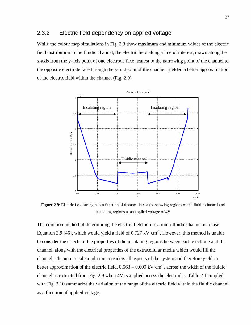
2.3.2 Electric field dependency on applied voltage
While the colour map simulations in Fig. 2.8 show maximum and minimum values of the electric
field distribution in the fluidic channel, the electric field along a line of interest, drawn along the
x-axis from the y-axis point of one electrode face nearest to the narrowing point of the channel to
the opposite electrode face through the z-midpoint of the channel, yielded a better approximation
of the electric field within the channel (Fig. 2.9).
Figure 2.9: Electric field strength as a function of distance in x-axis, showing regions of the fluidic channel and
insulating regions at an applied voltage of 4V
The common method of determining the electric field across a microfluidic channel is to use
Equation 2.9 [46], which would yield a field of 0.727 kV·cm-1
. However, this method is unable
to consider the effects of the properties of the insulating regions between each electrode and the
channel, along with the electrical properties of the extracellular media which would fill the
channel. The numerical simulation considers all aspects of the system and therefore yields a
better approximation of the electric field, 0.563 – 0.609 kV·cm-1
, across the width of the fluidic
channel as extracted from Fig. 2.9 when 4V is applied across the electrodes. Table 2.1 coupled
with Fig. 2.10 summarize the variation of the range of the electric field within the fluidic channel
as a function of applied voltage.
Fluidic channel
Insulating region Insulating region

28
Applied
Voltage [V]
Minimum
Electric Field
[kV·cm-1
]
Maximum
Electric Field
[kV·cm-1
]
Range, [kV·cm-1
]
4 0.563 0.609 0.046
8 1.126 1.219 0.093
12 1.689 1.828 0.139
16 2.252 2.437 0.185
20 2.815 3.046 0.231
24 3.377 3.656 0.279
28 3.940 4.265 0.325
32 4.507 4.532 0.025
36 5.439 5.473 0.034
40 6.043 6.093 0.050
44 6.592 6.702 0.110
48 7.252 7.311 0.059
Table 2.1: Dependency of electric field range on applied voltage

29
Figure 2.10: Plot of electric field dependency on applied voltage as obtained from COMSOL simulations
Based on the numerically approximated values in Table 2.1, the applied voltage chosen for the in
vitro studies in the project was 32V since it yields the least variation of the electric field across
the width of the channel and exceeds the minimum required field (0.33-1kV·cm-1
) at the poles of
the cell closest to the electrodes to initiate irreversible electroporation. Furthermore, by Equation
2.4, the field produced by this applied voltage is capable of inducing transmembrane potentials
greater than the required threshold for lysis at positions on the plasma membrane further away
from the electrodes, up to ~ θ = 820. This results in pore creation on ~90% of the cell‟s surface,
assuming the cell to be spherical. When considering nuclear membrane integrity, the electric
field generated by this applied voltage, would generate a maximum transorganelle potential of ~
0.9V on a 2µm sized nucleus, which is insufficient to cause rupture.
2.3.3 Determination of heat transfer to cell during lysis
Modeling the system as a capacitor
While COMSOL simulations have determined there is minimal resistive heating to the region of
the channel between the electrodes, if the electrode – insulator – microchannel system is
considered as a parallel plate capacitor (Fig. 2.11), with each region between the electrodes a
different dielectric material, then the amount of energy deposited to a cell in that region can be
30
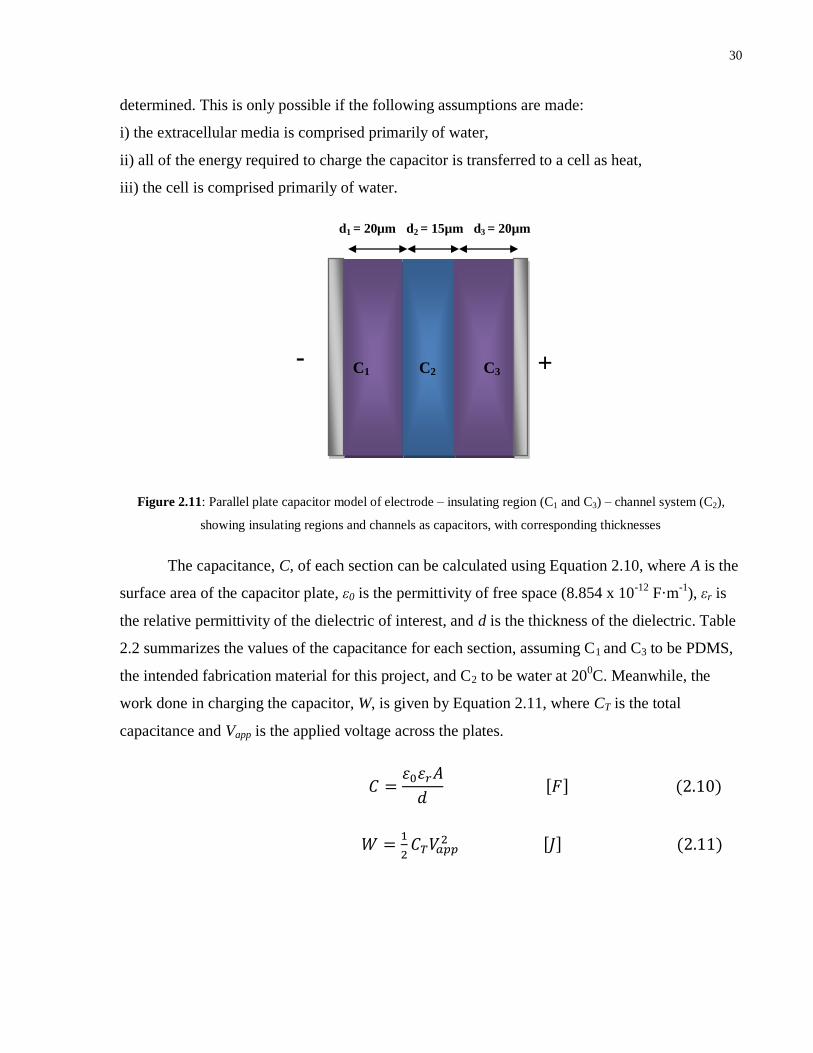
determined. This is only possible if the following assumptions are made:
i) the extracellular media is comprised primarily of water,
ii) all of the energy required to charge the capacitor is transferred to a cell as heat,
iii) the cell is comprised primarily of water.
Figure 2.11: Parallel plate capacitor model of electrode – insulating region (C1 and C3) – channel system (C2),
showing insulating regions and channels as capacitors, with corresponding thicknesses
The capacitance, C, of each section can be calculated using Equation 2.10, where A is the
surface area of the capacitor plate, ε0 is the permittivity of free space (8.854 x 10⁻¹²
F·m-1
), εr is
the relative permittivity of the dielectric of interest, and d is the thickness of the dielectric. Table
2.2 summarizes the values of the capacitance for each section, assuming C1 and C3 to be PDMS,
the intended fabrication material for this project, and C2 to be water at 200C. Meanwhile, the
work done in charging the capacitor, W, is given by Equation 2.11, where CT is the total
capacitance and Vapp is the applied voltage across the plates.
C3 + - C1 C2
d1 = 20µm d2 = 15µm d3 = 20µm

31
Material Relative
permittivity,
εr
Surface area (A) of
electrode (150µm x
20µm) [m2]
Thickness (d)
[m]
Capacitance [F]
C1 2.67 3 x 10⁻⁹
20 x 10-6
3.54 x 10⁻¹⁵
C2 80.1 3 x 10⁻⁹
15 x 10-6
1.42 x 10⁻¹³
C3 2.67 3 x 10⁻⁹
20 x 10-6
3.54 x 10⁻¹⁵
Table 2.2: Calculated values of the capacitance of each dielectric layer
The total capacitance is 1.75 x 10⁻¹⁵
F and with an applied voltage of 32V, Equation 2.11
determines the charging energy to be 8.96 x 10⁻¹³
J. Based on assumption (ii), Equation 2.12
calculates the change of temperature, ΔT, of a cell within the region of the microchannel between
the electrodes to be 2.14 x 10⁻⁴
K, when the mass of the cell, m, is assumed to be 1ng and its
specific heat capacity, c, to be 4186 J·kg-1
·K-1
. This estimation confirms that when the system is
modeled as a parallel plate capacitor, even in an extreme case where all of the energy stored in
the capacitor is transferred to the cell, the corresponding change in temperature is negligible.
Consequently, the electric field required to perform plasma membrane lysis is not expected to
produce thermal effects in the cell such as protein denaturation.
[ ]
Modeling the cell as a resistor
Simulations have shown that due to the insulating nature of the material separating the electrodes
from the microchannel, there is negligible resistive heating; however, the intended material is a
dielectric and has a breakdown voltage of 21.2V·µm-1
[56]. As a result, the extracellular media
and the cell can become a part of the current carrying circuit when the breakdown voltage is
exceeded, which would require a voltage of 424V since the material in the electrode to channel
gap is modeled as 20µm. Equation 2.13 is a combination of Joule‟s law and Ohm‟s law and

32
determines the energy, Ec, dissipated to a cell, of resistance, R, in time, t, when a current, I,
passes through the cell.
Assuming a short time duration of 100µs as commonly used in electroporation, an arbitrary
current of 5mA, and cell resistance of ~ 1 x 10⁴Ω, the energy dissipated is calculated to be 2.5 x
10-5
J, which would result in a temperature increase of 5972.3K. While this value is extremely
high, it is based on the assumption that all of the energy dissipated to the cell is transformed into
heat and that the system is 100% efficient. Since the applied voltages anticipated to be used in
this project do not approach the breakdown voltage of the dielectric, the system is not expected
to act as a complete current carrying circuit, thus the cell would not experience any resistive
heating. Additionally, pulse durations of 100µs to be used in this project are much greater than
the charging time of the plasma membrane (~100ns), and are yet small enough to prevent a large
amount of energy to be deposited to the cell.
2.4 Conclusion
This chapter has explored the theoretical basis for selective lysis of the plasma membrane via
electrical lysis and has compared this method to other current techniques available for single cell
lysis. By gaining an understanding of electrical lysis by both DC and AC electric fields and
weighing their pros and cons, a DC electric field was chosen for all in vitro work, to be discussed
in Chapter 4. COMSOL simulations provided a numerical approximation of the electric field
distribution within a microfluidic channel due to an applied voltage across a pair of electrodes,
while also demonstrating the heterogeneity and homogeneity of the electric field based on
commonly used 3-D electrode structures, and those intended for use in this project. Furthermore,
the simulations show that at an applied voltage of 32V, the electric field produced is large
enough to surpass the threshold transmembrane potential required for lysis, and there is minimal
variation of the field across the width of the channel. Consequently, this applied voltage, with a
pulse duration of 100µs, which is greater than the required charging time for the plasma
membrane, will be used for all in vitro studies in this project.

33
Chapter 3 Fabrication of microfluidics device with integrated electrodes for
single cell lysis
3.1 Introduction
3.1.1 Design requirements of a single cell microfluidic device
Channel geometry for cell confinement
Microfluidic devices designed and developed for the purpose of single cell analysis should
ensure that the fluidic channels are slightly wider than the diameter of the cells of interest to
assist in the confinement of cell movement to one direction along the channel. Additionally, in
regions where cells may be interrogated and their contents analysed, further narrowing of the
fluidic channel would encourage analyte flow along the channel and reduce diffusion laterally
within the channel.
There exists an abundance of microfluidic devices designed for single cell capture,
ranging from microfabricated physical cell traps situated both perpendicular to and lying on the
base of the fluidic channel [57, 58], micro-pillars standing vertically in the channel [54],
complex systems of pneumatic pumps and valves that control cell positioning within channels
[23], tapered fluidic channels that confine cell movement and act as a trap [24], dielectrophoretic
traps [25], and optical tweezers [24]. The challenge posed to the former devices is the ability to
confine analytes and limit diffusion after the cell has been lysed or interrogated in some way, due
to the fabrication limits of the device. Meanwhile, tapered channels limit the flow of the buffer
solution adjacent to the cell and limits transverse diffusion of analytes while promoting flow
longitudinally. This chapter will present a tapered channel geometry with the inclusion of a
region where cell lysis and future analyte separation will occur, referred to as the injector
structure.
Integration of electrodes
For the purposes of electrical lysis, integrated electrodes in a microfluidic device are required to
either pass a direct current across the cell by being in contact with the cell [54], or by creating an
electric field in the vicinity of a cell [27]. As outlined in Chapter 2, integrated electrodes are

34
advantageous if designed to be 3-D structures [28, 53] to create an electric field which interacts
with a larger cell surface as opposed to electrodes which are 2-D producing fields that only
impact one part of a cell [27]. Most 2-D electrodes are fabricated by a deposition process or
excimer laser mediated cutting as demonstrated by Xu et al [59] using ITO and other similar
materials, while 3-D electrodes usually require a complex fabrication method to place platinum
or titanium wires, or photolithographic development of chromium and silver electrodes onto
glass [54]. In this chapter, a novel method of integrating 3-D microelectrodes in close proximity
to fluidic channels and capable of extending a homogenous field over a larger cell surface of a
single cell will be demonstrated.
3.1.2 UV photolithography as a fabrication tool
The process of photolithography entails the selective removal of parts of a thin photo sensitive
film, referred to as a photo resist, by transferring desired patterns from a photo mask using light
of a specific wavelength. Prior to exposure, the resist is distinguished as being either positive or
negative, depending on the way it is developed following irradiation, with the former becoming
insoluble in photopolymerized regions, and the latter soluble where exposed. Viscosity of the
resist is a significant determining factor of film thickness, which in turn determines the aspect
ratio, referring to the ratio of the width to height of the structures being fabricated [60].
This method has been used for over a decade as a fabrication tool for microfluidic
devices [61], with the resist being deposited on a variety of substrates including glass [62],
silicon wafers [63], and metals [64]. While the latter two have shown good adhesion and thermal
expansion coefficient match to photo resists, they are significantly more expensive, while glass
can be treated to improve its substrate qualities and is less expensive. In the same respect, a
plastic photo mask is often preferred [63] since it is cheaper and allows more masks to be created
and designs to be implemented for the equivalent cost of having a single metal mask, typically
quartz-chrome, designed for one geometric pattern [65]. However, plastic masks, produced by a
printing process, are unable to achieve the same spatial resolution and fine details as metal masks
which are produced by laser writing.
Following photolithography, structures can either be used directly as microfluidic devices
[66] or in a soft lithography process in which another material, commonly PDMS, is casted onto
the photo resist to create an inverse of the structures [63]. PDMS, while naturally hydrophobic,

35
has demonstrated good biological compatibility due to it being non-toxic [67, 68], structurally
flexible, inert, allows for rapid prototyping [63], and consequently has become the most
commonly used material in which microfluidic devices are fabricated.
Other fabrication tools exist to create microfluidic devices, including laser
micromachining [24], hot embossing [69] and direct write laser photolithography [70] among
others; however, while the latter of these methods offer better resolution than ordinary
photolithography, they are expensive, time consuming and for the purposes of this project,
incompatible for the overall program. This chapter reports on an improvement to the standard
photolithography procedures yielding minimum structure sizes of 5µm using a plastic photo
mask and glass substrate.
3.2 Materials and Methods
3.2.1 Photo mask production and optimization
Mask lay-out as produced by computer-aided design
Designs were sketched using closed rectangles and circles in commercial AutoCAD 2008
software (Autodesk, Inc., San Rafael, CA, USA), as described similarly by the Whiteside group
[61, 71]. Two-dimensional structures were drawn to represent the outline of the intended device
with fluidic channels targeted to be 35µm wide, at least twice the diameter of a typical
eukaryotic cell (~10-15µm) and to enable pressure driven flow. In the region designated as the
injector structure, the channel was reduced to a width of 15µm over a distance of 100µm to
permit single cells to sequentially enter the electrode zone at any given time. Beyond the
electrode zone the channel was further tapered to 7µm over 250µm to confine the flow of
analytes post lysis specifically to confine horizontal diffusion and encourage diffusion along the
channel. For this work, a funnel shaped design allowed a single cell to be held in place at the
centre of the electrodes as depicted in Fig. 3.1(a). The overall length of the fluidic channel was
targeted to be 10mm with a port hole, 1.25 mm in diameter, drawn at one end to be used for
fluidic access.
Channels to be converted into electrodes were designed perpendicular to the injector
structure and offset from the fluidic channel by 20µm along the x-axis. A width of 150µm,
centred at the funnel shaped region of the fluidic channel, was selected to enable the resulting

36
electric field to completely encompass a cell being held in this region as shown in Fig. 3.1(b).
The length of each electrode was planned to be 4.25mm having a 1.5mm diameter filling port
and a 260µm x 40µm air flow channel angled at 550 to the end closest to the fluidic channel. The
air flow channel terminates with a 1mm diameter port hole and along with the initial 400µm
wide region section of each electrode will allow for easier integration of the electrode material
upon device fabrication.
Figure 3.1: (a) Schematic AutoCAD drawing of integrated microfluidic device (b) Injector structure region
Printing and characterization of photo masks
Three different commercial printing companies were solicited, namely Norwood Graphics Inc.
(Toronto, ON, Canada), Pacific Arts and Designs (Toronto, ON, Canada) and The Photoplot
Store (Colorado Springs, CO, USA), to print the mask lay-out designed in AutoCAD at the
highest possible resolution to accommodate the micron sized features and gaps on the mask.
Each vendor printed the photo masks using particular photoplotters and photo film providing
varying degrees of resolution. Figure 3.2 shows a typical photoplot file that was converted from
the initial CAD drawing prior to the production of the true photo mask with the white regions
representing the transparent region through which light will pass.
(b)
Electrode Cell funnel
(a)
4.25mm
1.25mm
150µm
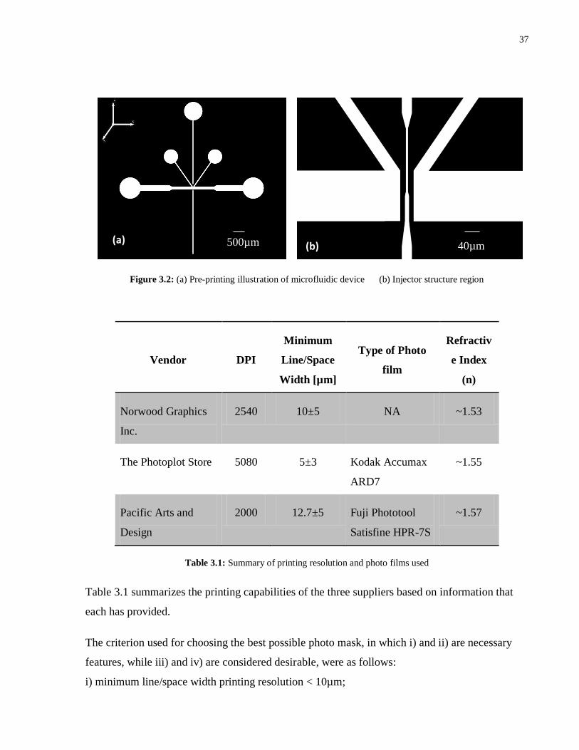
37
(b)
Figure 3.2: (a) Pre-printing illustration of microfluidic device (b) Injector structure region
Vendor DPI
Minimum
Line/Space
Width [µm]
Type of Photo
film
Refractiv
e Index
(n)
Norwood Graphics
Inc.
2540 10±5 NA ~1.53
The Photoplot Store 5080 5±3 Kodak Accumax
ARD7
~1.55
Pacific Arts and
Design
2000 12.7±5 Fuji Phototool
Satisfine HPR-7S
~1.57
Table 3.1: Summary of printing resolution and photo films used
Table 3.1 summarizes the printing capabilities of the three suppliers based on information that
each has provided.
The criterion used for choosing the best possible photo mask, in which i) and ii) are necessary
features, while iii) and iv) are considered desirable, were as follows:
i) minimum line/space width printing resolution < 10µm;
40µm 500µm (a)

38
ii) minimum ink spray onto clear regions targeted as microstructures;
iii) high OD at 365nm in the region of the printed black ink, with %T < 0.01%;
iv) low OD at 365nm in the clear transparent region, with %T > 50%;
Measurements of the light absorption of each type of photo film at 365nm were made so
as to determine which would allow the least amount of attenuation of the UV beam during
irradiation. A thin strip of each type of photo film was positioned on the inner wall of a 4.5ml
PMMA cuvette (VWR International, Mississauga, ON, Canada) and placed into a CARY 300
Bio spectrophotometer (Varian, Inc., Palo Alto, CA, USA) to measure the OD of the film. The
absorbance of both the transparent and the black printed parts of the photo mask were quantified
over the range 250nm to 500nm to determine the effect of both the film and the ink on the
transmission of light at the wavelength of interest, 365nm.
Using an Axiovert 200M (Carl Zeiss, Toronto, ON, Canada) inverted microscope with a
mounted CoolSNAP Pro camera (Media Cybernetics, Bethesda, MD, USA), offering an
additional 10X magnification for image acquisition and packaged with Image-Pro Plus analysis
software, images were acquired of the microstructures on the printed photo mask. The software
allowed measurements to be made of structure widths and lengths which were then compared to
the CAD drawn features to determine how well the features are reproduced. Additionally, the
images highlighted regions in which the ink spray had spread to the microchannel regions during
printing and combined with the measurements would give a more accurate view of what the true
resolution of each mask is.
3.2.2 Preparation of glass substrates
Piranha treatment of glass slides
Soda-lime glass, primarily composed of SiO2 (~73%), of dimensions 75mm x 20mm x 1mm
(Ted Pella Inc., Redding, CA, USA) were used as the substrate for photolithography. Since glass
is hydrophobic and manufactured slides may have organic residues due to handling, slides were
first exposed to high pressure air to remove dust particles and cleaned by immersing in a piranha
solution, a 3:1 volumetric ratio of 99% H2SO4 (Sigma-Aldrich Ltd., Oakville, ON, Canada) and
30% H2O2 (Sigma-Aldrich Ltd., Oakville, ON, Canada) [72, 73]. The solution hydroxylates the
glass surface thus making it hydrophilic and increasing the number of silanol groups [74]. While
working in a chemical fume hood, slides were placed in a large Pyrex baking dish and
39
submerged with 150ml of H2SO4 after which 50ml of H2O2 was poured into the dish creating a
highly exothermic reaction reaching about 1200C. After 10 minutes of piranha treatment, the
slides were removed individually from the solution and washed in 2 sequential baths of
18.2MΩ·cm deionized water for 1 minute each. This step aids in the removal of any residual
traces of the H2SO4 - H2O2 reaction. Slides not being used immediately were stored in a large
beaker with deionized water and sealed with parafilm. Prior for use as photolithographic
substrates, glass slides were submitted to a dehydration bake on a hotplate at 2000C for 30
minutes.
Spin coating photoresist with improved adhesion
SU-8 2025 (MicroChem Corp., Newton, MA, USA) was the resist used for UV
photolithography. It is a thick, negative-tone, epoxy-photoplastic that is capable of reproducing
structures with high aspect ratio [60, 75]. It has been established that to obtain a homogenous and
stable coating of SU-8 onto the substrate, there must be sufficient wetting [76], as untreated glass
has poor adhesion properties with SU-8 [66, 75] causing structures to become tilted and to
delaminate easily. Others have attempted to circumvent this problem by using a very thin (~2-
5µm), highly polymerized SU-8-2 layer, referred to as a seeding layer, between the true SU-8 to
be used in fabrication and the glass [77]. However, a known adhesion promoter [78], OmniCoat
(MicroChem Corp., Newton, MA, USA), was used as a sacrificial layer between the glass
substrate and the SU-8. While a complete understanding of chemical nature in which OmniCoat
aids in adhesion is difficult due to commercial reasons, it is generally inferred that its purpose is
to decrease the interfacial stress, which is a known delaminating factor between the SU-8 and the
glass substrate.
Using a WS-400-6NPP-LITE spin coater (Laurell Technologies Corp., North Wales, PA
USA), several drops of OmniCoat, amounting to 2ml, were placed on the glass substrate to
ensure maximum surface coverage as its thickness is of no importance [75]. It was spun for 5
seconds at 500 rpm with an acceleration of 100 rad·s-1
followed by a second spin cycle of 30
seconds at 3000 rpm accelerating at 300 rad·s-1
. These cycles created an OmniCoat layer of
approximately 20-30nm in thickness. The adhesion promoter deposition process was completed
by baking the substrate on a hotplate at 2000C for 1 minute and allowing it cool to room
temperature.

40
To achieve 20µm high structures within SU-8, 3ml of SU-8 2025 was deposited onto the
centre of the glass substrate over a sacrificial OmniCoat layer. The sample was spun at 500 rpm
for 15s with an acceleration of 115 rad/s followed by 4000 rpm for 30s with an acceleration of
342 rad/s as recommended by MicroChem Corp. (see Fig. 3.3).
Figure 3.3: Spin speed vs. film thickness curve for various photoresists (Adapted from [60])
Subsequently, the substrate then underwent a soft bake process at 650C and 95
0C, however, the
suggested times of 1 minute and 6 minutes respectively, were extended to 3 minutes and 20
minutes. The prolonged soft baking time allowed for maximum solvent evaporation which
avoids high film stress during post-exposure baking [75, 76, 79]. Following UV
photopolymerization and post-exposure baking, samples of the thin SU-8 film were removed
with a scalpel and attached to a 3mm thick slab of PDMS using a drop of glycerol to promote
adhesion. The combination piece was then placed on its thin edge (3mm) on a no. 1 glass cover
slip (~0.13-0.17mm) and observed using the Axiovert 200M microscope and measurements of
the film thickness were made using Image-Pro Plus.

41
3.2.3 SU-8 exposure and development
UV exposure with reduced diffraction effects
Prior to UV exposure, samples were kept in a Petri dish wrapped in aluminum foil to avoid
premature photopolymerization and degradation from environmental light sources. The set-up of
the substrate and mask during UV irradiation is depicted in Fig. 3.4 showing first a 25mm x
80mm x 3mm (x, y, z) base layer of PDMS which acted as a dampener to the glass substrate in
the event of external vibrations. The next layer was a piece of printed black transparency of
equivalent x, y dimensions to the PDMS whose purpose was to reduce retro-reflection of the UV
light as it passed through the substrate. Figure 3.4(a) shows one configuration in which the photo
mask was placed directly on top of the SU-8 substrate with a small air gap in between, while (b)
shows an alternative method of having a thin layer of glycerine (Sigma-Aldrich Ltd., Oakville,
ON, Canada) acting as a gap and refractive index compensating media between the SU-8 and the
mask [80, 81]. The significance of this step will be discussed below in Section 3.3.3. Small
droplets of the glycerine were deposited on the underside of the mask which would be in contact
with the SU-8 and spread evenly using a lint free swab. The mask was then pressed firmly onto
the SU-8 to remove pockets of air and to ensure uniform flatness.
The light absorption by glycerine was quantified over the 250nm to 500nm range using a
CARY 300 Bio spectrophotometer. The liquid was placed into a 4.5ml PMMA cuvette, with path
length 10mm, and the OD at 365nm was determined.
Figure 3.4: Set-up of SU-8 substrate with photo mask for UV exposure with (a) air gap, (b) glycerine. Numbers in
bracket represent thickness of each layer and corresponding refractive index

42
A SÜSS MA6 mask aligner (SÜSS MicroTec, Garching, Germany) producing an output
of 16.5 ± 0.5 mW·cm-2
was used in soft contact mode to perform UV exposure of the substrate.
This mode caused the top surface of the mask to just touch the aligner‟s heavy glass plate
without any decompression of the SU-8 substrate. Different exposure times of 10s, 12.5s, 15s,
and 17.5s were tested for photopolymerization of SU-8 to determine an optimal time with or
without the glycerine layer that would yield structures of the highest resolution. The
recommended radiant energy per cm2 for a 20µm thick film was 150 - 160 mJ·cm
-2 [60] and
based on Equation 3.1, where ERAD represents the radiant energy, and P the power, this
corresponds to an exposure time, texp, of ~9.1 - 9.7s. Meanwhile, the exposure times investigated
correspond to energies of 165 mJ·cm-2
, 206.25 mJ·cm-2
, 247.5 mJ·cm-2
, and 288.75 mJ·cm-2
respectively. These values represent the exposure before attenuation by the photo mask and
glycerine.
[mJ] (3.1)
Post exposure baking and substrate development
Immediately following UV exposure, SU-8 substrates were placed on a hotplate at 650C, for 1.5
minutes, after which they were transferred to a second hotplate at 950C for a baking time of 30
minutes. These times were longer than the recommended times from MicroChem Inc. of 1
minute and 6 minutes respectively to accommodate the thermal polymerization process that
would improve the resolution of the SU-8 structures in regions that were not adequately
photopolymerized, by continuing the cross-linking process [76, 79]. Since there is a large
thermal expansion coefficient mismatch between SU-8 (52 ppm K-1
) and glass (9 ppm K-1
), for
cool-down, substrates were placed on a hotplate at 650C for 15 minutes to minimize stress being
imprinted in SU-8 at the material interface [75] before being placed into a Petri dish at room
temperature.
Chemical development was performed by immersing substrates individually in 10ml of
SU-8 developer (MicroChem, Newton, MA, USA) for 1 minute while agitating rigorously. This
was followed by a spray rinse with 99% isopropanol (Sigma-Aldrich Ltd., Oakville, ON,
Canada) for 10-15 seconds and a final controlled high pressure air drying step to dry the
substrate and remove residual isopropanol while ensuring no SU-8 lift off from the substrate.

43
Prior to the PDMS microchip development, the substrate, referred to henceforth as the SU-8
master, was examined under the Axiovert200M microscope to determine the resolution of the
structures and the shrinkage of structure width which may have occurred during exposure and
development.
Measurement of side wall angle of SU-8 structures
Due to the rigidity of the SU-8 microstructures, a direct measurement of their x-z angularity was
not possible without damaging and delaminating the structures in the process. Instead, the SU-8
master was placed on a flexible polycarbonate sheet with the structures facing upward and a rigid
acrylic frame, 4mm deep, surrounded the master. 20ml of PDMS mixture was made from a 10:1
(V:V) base to curing agent of Sylgard 184 elastomer (Paisley Product Inc., Toronto, ON,
Canada) and degassed using a vacuum desiccator (Bel-Art Products, Pequannock, NJ, USA) for
20 minutes. PDMS was cast onto the SU-8 master and 350g aluminum weights were used to
keep the frame in place and to prevent prepolymer PDMS from leaking out while the
polycarbonate sheet (P & A Plastics Inc., Hamilton, ON, Canada) was placed on a hotplate at
700C for 1.5 hours. The flexible sheet enabled the SU-8 master with the casted PDMS to be
easily removed without damaging the SU-8 master or the PDMS. The cured PDMS piece,
referred to as the PDMS master, was 4mm in height given by the depth of the acrylic frame and
was slowly peeled away from the SU-8 master to prevent the SU-8 structures from lifting off the
glass substrate and becoming embedded in the PDMS.
A transverse slice was made through the PDMS master to obtain a cross sectional view of
the fluidic and electrode channels and observed using the light microscope. Using the ImagePro
Plus software, the side wall angles were measured as illustrated in Fig. 3.5. To properly
characterize the variation of the side wall angle as a function of channel width, SU-8 structures
of widths ranging from 5µm to 100µm were subjected to the above mentioned procedure and a
graph of channel width versus side wall angle was plotted for structures created with and without
glycerine as the gap compensating media.

44
(
)
Figure 3.5: Illustration of cross sectional view of a microfluidic channel and method of measuring side wall angle
3.2.4 Device fabrication by rapid prototyping of PDMS
Production of rigid epoxy master
The SU-8 master was replicated in PDMS by casting as previously described, (Section 3.2.3)
producing a PDMS master, inverse to the SU-8 master, with valleys or channels where ridges
and structures exist on the SU-8 master. Due to the fragile nature of the SU-8 master, a rigid
epoxy master was fabricated which would maintain the resolution of the original master and
could be used repeatedly without degradation of microstructures. With the channels facing
upwards, the PDMS master was placed in a 6mm deep rectangular receptacle made of the same
elastomer, and 20ml of a single component UV curable epoxy, OG 169 (Epoxy Technology,
Billerica, MA, USA), was poured onto the master. This was cured using an in-house UV light
box with an irradiance of 2.0 ± 0.2 mW·cm-2
for 45 minutes to create the epoxy master. Due to
the flexibility of the PDMS receptacle, the final master was easily removed after curing.
PDMS

45
Figure 3.6: Illustration of multi-step soft lithography process
With this approach, rapid production of PDMS microfluidic chips was achieved in less
than 1.5 hours, first by pouring 10ml of prepolymer PDMS into the epoxy master and degassing
for 20 minutes, immediately followed by a 1 hour baking period at 700C, and careful removal
from the epoxy master, to ensure all fine details of the fluidic channels remain intact. Figure 3.6
illustrates the complete soft lithography process which allows rapid prototyping of the PDMS
chip. Access ports for fluidic entry and control, air flow exit and electrode filling were created
using Harris Uni-core punches (Ted Pella Inc., Redding, CA, USA) of internal diameters 0.5mm,
1.5mm and 2.0mm respectively, while a 3.0mm punch was used to create a reservoir at the
opposite end of the fluidic channel away from the entry and control port.
Verification of wall uniformity by confocal microscopy
While the method described in Section 3.2.3 allows only a small number of single point views
and measurements of the side wall angle, multiple 3-D images of the microfluidic channels were
obtained using confocal microscopy after filling the fluidic and electrode channels with different
fluorescent dyes. The electrode and their air outlet channels were filled with a 0.1mM solution of
Rhodamine 123 (excitation = 505nm, emission = 560nm) (Invitrogen Inc., Burlington, ON,

46
Canada), while a 0.1mM solution of Hoechst 33342 (excitation = 350nm, emission = 461nm)
(Invitrogen Inc., Burlington, ON, Canada) filled the fluidic channel. Using a Zeiss LSM 510
META NLO inverted microscope (Carl Zeiss, Toronto, On, Canada) with a 10x objective, a Z-
stack of the fluorescent channels in the vicinity of the injector structure region was obtained at
2µm slice intervals.
PDMS bonding by air plasma
To enclose the network of channels, a fourth surface was required as the moulded PDMS chip
provides only three walls. This surface was fabricated by spin coating prepolymer PDMS for 40s
at 750rpm onto a no. 1 glass cover slip to create a 100µm thin membrane [82] which was baked
on a hotplate at 700C for 1 hour to cure. The thickness of the membrane was verified using
Image-Pro Plus as previously described (see Section 3.2.2). Due to the high pressures that can
exist within the channels, especially during the electrode filling process, an irreversible seal was
necessary between the PDMS chip and PDMS cover slip. By exposing the two surfaces to an air
plasma treatment, an increase in the surface free energy and Silanol groups are created,
permitting covalent bonding when the two PDMS substrates are brought into conformal contact,
thus forming a tight, irreversible seal [68, 83].
Traditionally, vacuum plasma systems with a controlled oxygen flow are used for this
bonding process, however, a less cumbersome, hand held corona treater was used in this work
which operates in room air at atmospheric pressure [84]. In the confines of a fume hood, a BD-
20AC portable device (Electro-Technic Products Inc., Chicago, IL, USA) was held in a fixed
vertical position with a retort stand (Fig 3.7) while the two PDMS parts were placed flat on a
motorized stage moving back and forth at a speed of 10 ± 1 mm·s-1
. The PDMS surfaces were a
distance of 4.0 ± 0.2mm from the wire electrode of the corona treater and exposed to the plasma
for 8 passes, totalling 45 seconds, after which the PDMS chip was manually pressed lightly
against the thin membrane to complete the sealing process. These PDMS devices are rendered
hydrophilic for a brief period after the plasma treatment and a 12 hour period was allowed before
they were used for any microfluidic experiments.

47
Figure 3.7: Corona treater with PDMS chip and spin coated cover glass on a motorized stage
3.2.5 Material characterization of integrated electrodes
Composite PDMS with carbon
The design of the microfluidic chip in this project allows for the integration of electrodes by
filling a suitable material into the channels intended as electrodes. Xiu et al [85] reported a
method of incorporating carbon black particles, which are known to have good electrical
properties (ρ ≈ 0.2Ω·cm) [86], into prepolymer PDMS to create conducting composites. Since
PDMS, even at higher than normal viscosities after mixing with carbon, would be straight
forward to integrate into the electrode channel to create an almost seamless electrode, a similar
method was followed by mixing Vulcan XC72R carbon black (Cabot Corp., Boston, MA, USA)
into prepolymer PDMS with concentration based on weight. Composites of mixing ratios 5%,
10% and 15% by weight of carbon to PDMS were created by adding the powdery carbon black
in 0.1g increments to the PDMS and mixing vigorously to promote uniform dispersion of the
carbon particles within the composite. This was necessary since carbon black has a density of
0.096g·cm-3
compared to that of PDMS, 0.965 g·cm-3
.
Corona treater
Motorized stage
Electrode wire
PDMS chip
Spin coated
cover glass

48
Different lengths of tubing (Cole-Parmer Inc., Montreal, QC, Canada), ranging from 3cm
to 12cm, each with an inner lume of 0.81mm, were filled with each of the composites. A 20mm
length of copper wire of diameter 250µm (Consolidated Electronic Wire & Cable, Franklin Park,
IL, USA), was inserted at each end and cured on a hotplate at 700C for 2 hours to create carbon
based PDMS wires (Fig. 3.8a), and their resistance was measured using a digital multimeter
(Fluke Electronics, Mississauga, ON, Canada) . By plotting the resistance, R, as a function of
length, l, the electrical resistivity, ρ, was determined by multiplying the slope of the graph and
the cross sectional area, A, of the tubing, following Equation 3.2, which assumes that the
composite is a uniform electrical conductor . Equation 3.2 does not consider the random
arrangement of the carbon particles within the PDMS matrix.
The integrated electrodes were fabricated by filling the carbon-PDMS composite into the
electrode channels of the microfluidic device using a 10ml syringe under high pressure via the
designated filling ports, inserting copper wire and curing as described above. Effectiveness of the
filling process throughout the electrode was observed under a light microscope.
Electrically conductive epoxies and pastes
Electrical properties of manufactured compounds embedded with metals, giving them the ability
to conduct, were also investigated and integrated into the microfluidic device. Table 3.2
summarizes the properties of the different epoxies and pastes tested as given by the
manufacturers that were used as integrated electrodes.

49
Property
Product Name
SS-25M SS-25M + OMS Silver Paste Plus Silver Conductive
Epoxy
Manufacturer
Silicone Solutions,
Twinsburg, OH,
USA
Silicone Solutions,
Twinsburg, OH,
USA + Atelier
D‟art Hade &
Rodier, Granby,
QC, Canada
SPI
Supplies/Structure
Probe Inc., West
Chester, PA, USA
MG Chemicals,
Surrey, BC,
Canada
Description
-Single part epoxy
-Moisture curing
RTV
-Single part epoxy
-Moisture curing
RTV
-1:5 volumetric
ratio of SS-25M to
OMS†
-Single part paste
-Uniform particle
distribution
-Moisture curing
- Two part epoxy
- Moisture curing
Conductive Filler 98% Nickel and
Graphite
Nickel and
Graphite
~72% Silver ~45% Silver
Particle Size [µm] 2-15 2-15 0.3-0.6 1-5
Viscosity [cps] 100,000 NA ~70,000 ~60,000 (mixed)
Electrical
Resistivity (ρ)
[Ω·cm]
6 x 10⁻²
NA 3 x 10⁻⁵
3.8 x 10⁻¹
Electrical
Conductivity (σ)
[S·cm-1
]
16.7 NA 3.33 x 10⁴ 2.63
† - odourless mineral spirit
Table 3.2: Properties of electrically conductive epoxies and pastes used as integrated electrodes

50
Each compound was filled into different lengths of tubing and underwent an overnight
curing period, followed by a measurement of the resistance as described previously in Section
3.2.5. Their resistivity was also extracted from the slope of the resistance as a function of length,
according to Equation 3.2. The filling process was carried out in the same manner as described
for the carbon-PDMS composite and the resistance of the integrated electrode was also measured
within the microfluidic chip. Fig 3.8c illustrates the approach selected by inserting a 20mm
length of copper wire (diameter) through the PDMS to make contact with the tip of the electrode
proximal to the fluidic channel.
Figure 3.8: a) Tubing filled to measure resistance b) Cross sectional view and c) top view of chip with electrode
filled; d) Cross sectional view of chip showing resistance measurement with inserted copper wire
Injection moulding using molten solders
A modification to the system of fabricating micro electromagnets within a PDMS environment
as described by Siegel et al [87] allowed micro wires to be embedded in the previously described
PDMS microfluidic device creating the integrated electrodes. This is possible as PDMS is
thermally and mechanically stable up to 3000C [88]. A 0.1M solution of 3-
mercaptopropyltrimethoxysilane (Sigma-Aldrich Ltd., Oakville, ON, Canada) in acetonitrile
(Sigma-Aldrich Ltd., Oakville, ON, Canada) was injected into the intended electrode channel
and stored at room temperature for 1 hour to allow the solvent to evaporate. This silane
compound coats the channel, reducing its surface free energy and making it wettable to the
molten solder.
l
A
(a)
(b) (c)

51
Concurrently, 2g of 99.9% In solder (AIM Solders Inc., Cranston, RI, USA) was placed
in a metal tipped 10ml glass syringe (Cole-Parmer Inc., Montreal, QC, Canada) wrapped in
silicone heating tape (HTS/Amptek Company, Stafford, TX, USA) and heated to ~2000C,
melting the solder (melting point = 1570C). After the 1 hour silanizing period, the microfluidic
device was placed on a hotplate at 2250C and molten solder was injected into the electrode
channel by inserting the tip of the syringe into the filling port and applying manual pressure to
the syringe. After complete filling is observed, a 20mm length of 250µm diameter copper wire
was inserted into each port and the device was removed from the hotplate to cool at room
temperature bonding the copper wire firmly. This method was repeated using 57Bn25In17Sn
solder (AIM Solders Inc., Cranston, RI, USA) which has a melting point of 790C.
Since it was difficult to manipulate molten solder, the method of measuring the resistance
of the material by inserting it into different lengths of tubing (Section 3.2.5) was not applied
here. Instead, the resistance of a solid bulk solder block, 55mm x 4mm x 3mm, was measured
and the resistivity calculated using Equation 3.2. The resistance of the integrated electrode was
measured by making contact with the electrode tip by inserting a piece of copper wire through
the PDMS as previously described.

52
3.3 Results and Discussion
3.3.1 UV absorbance and micrograph resolution of photo masks
The thickness of each type of photo mask investigated, along with their absorbance at 365nm
extracted from Figures 3.9 (b), is shown in Table 3.3
Figure 3.9: a) Absorbance as a function of wavelength for printed parts of photo mask, b) Absorbance as a function
of wavelength for transparent part of each photo mask
a) b)

53
Vendor Thickness/µm OD365nm
(Black ink)
OD365nm
(Clear
transparency)
Norwood Graphics
Inc.
85±5 6.014 0.235
The Photoplot Store 175±5 5.950 0.202
Pacific Arts and
Design
175±5 6.723 0.255
Table 3.3: Thickness and OD measurements of 3 different photo mask
Each of the three photo masks demonstrate negligible light transmission (~0.0001%)
through the black ink while the clear region transmits >55% of the light, thus satisfying the two
secondary criteria. As a result, the determining factor for the mask choice was made based on
the micrograph images of the masks (Fig. 3.10) which determined whether the imperative criteria
were met. These images showed that while the Norwood mask was reported to have a minimum
resolution of 10µm, the edge features along the intended channel region were poor and there was
significant ink spray in clear regions. The Pacific Arts mask had poor resolution at 12µm and
was unable to achieve the targeted CAD features less than 10µm. Meanwhile, the Photoplot
Store mask exhibited significantly better edge features, minimal ink spray and combined with a
minimum line/width resolution of 5µm was determined to be the closest match to the imperative
criterion and was selected for all photolithographic experiments.

54
Norwood Photoplot Store Pacific Arts
Figure 3.10: Micrograph images of mask features from 3 suppliers (top - 10x objective; bottom - 20x
objective)
3.3.2 SU-8 spin coating and exposure
SU-8 spin coated thickness
The photo resist thickness was measured once monthly for 4 consecutive months and 5 samples
each time, to determine the consistency of the spin coater in producing a targeted 20µm
thickness of SU-8. Results indicated that the average thickness when spin coating was executed
as recommended in Fig. 3.3 was 20.6 ± 0.2µm.
Optimization of exposure times
The OD of the chosen photo mask (Photoplot Store) at the wavelength used for UV
photolithography was determined to be 0.202 (Table 3.3) in the clear region through which light
is transmitted. Meanwhile, the OD, AOD, of glycerine at 365nm for a 10mm path length, l, was
determine to be 0.0351, giving an absorption coefficient, α, of 0.00351mm-1
from Equation 3.3a.
By assuming that the layer of glycerine between the photo mask and the SU-8 is ~10µm, and the
experimentally determined absorption coefficient, the OD of the glycerine layer at 365nm was
3.51 x 10⁻⁵
. This confirms that the photo mask impacts the incident light reaching the SU-8 layer
40µm Bottom Images 140µm Top Images

55
due to absorption, while neither an air gap, nor a glycerine layer between the mask and the SU-8
results in any significant absorption.
(3.3a)
[mW.cm
-2] (3.3b)
It was previously stated that the irradiance of the mask aligner was 16.5mW·cm-2
.
However, according to one form of the Beer-Lambert law (Equation 3.3b), the irradiance
reaching the SU-8 substrate was calculated to be ~13.48mW.cm-2
. Consequently, the radiant
energy per cm2 for each of the times used during SU-8 photopolymerization determined by
Equation 3.1 has been summarized in Table 3.4.
Exposure Time
(s)
Radiant Energy per cm2
on photo mask [mJ·cm-2
]
(16.5mW.cm-2
irradiance)
Radiant Energy per cm2
on SU-8 [mJ·cm-2
]
(13.48mW.cm-2
irradiance)
10 165 134.8
12.5 206.25 168.5
15 247.5 202.2
17.5 288.75 235.9
Table 3.4: Initial and final radiant energy per cm2 due to absorption in photo mask
The recommended radiant energy per cm2 for a 20µm layer of SU-8 is 150-160mJ·cm
-2,
which would have required an exposure time of 11.1s-11.9s according to the adjusted irradiance
of 13.48mW·cm-2
. Three of the four exposure times used were greater than the recommended
value and as a result there is an overcompensation of the required radiant energy per cm2. This
ensures that there is adequate photopolymerization and cross-linking of the compounds in the
SU-8 photoresist. Based on the calculated radiant energies, an exposure time of 12.5s yields the
closest match to the recommended radiant energy, while it could be expected that the longer

56
exposure times may cause over-exposure of the SU-8 film, resulting in loss of feature
delineation and hence resolution [75].
Improvement of SU-8 resolution using glycerine
After developing the SU-8 structures, it was observed that SU-8 films subjected to 10s of
exposure time easily delaminated during the drying process, presumably due to inadequate
photopolymerization of the photoresist, particularly near the SU-8 – glass interface. Meanwhile,
micrograph images (Fig. 3.11a) of the developed SU-8 structures confirm that the edge features
of over-exposed exhibit poor resolution at times exceeding 12.5s when there is an air gap
between the photo mask and the SU-8 surface. However, as previously shown by Kang et al
[81], results indicate that the use of glycerine (Fig. 3.11b) as a gap and refractive index
compensating media improves the resolution of edge features by reducing diffraction effects
and allows minimum line widths of 5µm for the Photoplot Store mask to be maintained. Those
diffraction effects will be explored in greater detail when discussing the side wall angle
measurements.
12.5s 15s 17.5s
a) Without Glycerine
b) With Glycerine
40µm
Figure 3.11: Resolution improvement of SU-8 structures using glycerine for different exposure times

57
3.3.3 PDMS device development
Side wall angle and channel uniformity measurements
A significant improvement in the side wall angle of the PDMS channels was observed when a
thin layer of glycerine was used as a compensator removing the air gap between the photo mask
and the SU-8 surface. Micrograph images (Fig 3.12) provide examples of this phenomenon while
the plot of side wall angle as a function of channel width for the three exposure times (12.5s, 15s,
17.5s) confirms the angle improvement (Figure 3.13).
Figure 3.12: Micrograph images of PDMS channels showing side wall angle improvement with glycerine at an
exposure time of 12.5s
Figure 3.13: Side wall angle as a function of channel width for different exposure times
The ideal side wall angle, υ, is 900, and was not achieved for any of the exposure times, while
the angle increased with channel width. It asymptotically approached 86.50, 85
0 and 85
0 for
exposure times of 12.5s, 15s and 17.5s respectively while the slope of wall angle versus channel
width approached 0 for glycerine use compared to a gradient when an air gap was present.
Meanwhile, the terminal slope of υ as a function of channel width is still different from zero for
PDMS – Without Glycerine PDMS – With Glycerine
50µm 50µm
Without Glycerine With Glycerine

58
the samples without glycerine. The common feature with samples with and without glycerine
appears to be a lower side wall angle for structures with aspect ratios 1:2 or greater, representing
a narrower channel base than wall height.
With an air gap between the mask and SU-8 layer, the UV light passes from a refractive
index 1.45 (photo mask), to 1 (air), and finally 1.65 (SU-8). Refraction of the UV light due to the
refractive index mismatch between the layers does not apply to explain a wider upper region near
the surface of the photoresist, and a narrower structure near the base as the UV beam is well
collimated. Chuang et al [80] proposed an explanation for the side wall angle phenomena based
on Fresnel diffraction. The thinness of the photo mask and its lack of flatness creates an air gap
between the mask and the SU-8 surface while the edges of the mask patterns cause diffraction
effects, with a Fresnel number, u, determined by Equation 3.4, where x represents the width of
the slit, y is the vertical distance to the photo mask, and λ is the wavelength.
√
(3.4)
Due to a large y value when an air gap is present, the Fresnel number is close to 10,
resulting in significant diffraction [89], accounting for the „top hat‟ effect when exposure extends
laterally from the slit. With the air gap eliminated by glycerine (n = 1.47), which has a refractive
index close to that of the photo mask, the distance between the mask and the SU-8 surface is
reduced considerably, resulting in a larger Fresnel number which yields a more uniform
diffraction pattern. Equation 3.4 also supports both air gap and glycerine experimental
observations that the side wall angle, which is indicative of the degree of diffraction, is greater
when the slit size is small, since at these widths the Fresnel number will be even closer to 1. It
should be noted that while the glycerine decreases the Fresnel diffraction effects, it does not
completely eliminate it since a perfectly uniform gap distance, and infinitely long slit size would
be required to create side wall angles of 900 [81].
Z-stack analysis of channel uniformity
The 3-D images obtained by confocal microscopy verified that in the vicinity of the injector
structure, where the electrode channel is closest to the fluidic channel, there were no significant
structural deformities or aberrations along the viewable lengths of either channel that may cause
non-uniform fluid flow or obstruct cell movement. This was evident even in the narrowest fluidic

59
channel region (~5.5µm). Primarily, the images and cross sectional profile (Fig. 3.14) of the
intensity measured transversely across a channel, further confirmed that the side wall angle
remains uniform along the length of the channel due to the negligible ascending and descending
slope of the profile. These images also show that there were not leakage points between the
PDMS-PDMS bond on the base of the device, nor from the fluidic or electrode channels into the
surrounding PDMS structure.
Figure 3.14: (a) Central plane in the x-axis; (b) Central plane showing z-axis view (top), and y-axis view through
the fluidic channel (right); (c) Sample profiles through various regions
Resolution losses from CAD to PDMS device
The fabrication process to develop the PDMS microfluidic device is susceptible to several
possible stages of line width resolution losses. From the CAD design to the printed mask, losses
are expected due to the printer‟s inability to fully capture the fine features, while SU-8 expansion
due to the cross-linking and development process would also change the feature sizes [76]. Table
3.5 shows a comparison of the channel widths and separator gaps for the various steps of the
fabrication process.
(a)
(b)
(c)
150µm
150µm
FWHM = 5.3µm
FWHM = 28.8µm
FWHM = 139.7µm
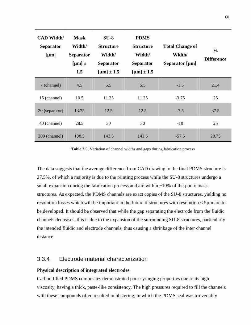
60
CAD Width/
Separator
[µm]
Mask
Width/
Separator
[µm] ±
1.5
SU-8
Structure
Width/
Separator
[µm] ± 1.5
PDMS
Structure
Width/
Separator
[µm] ± 1.5
Total Change of
Width/
Separator [µm]
%
Difference
7 (channel) 4.5 5.5 5.5 -1.5 21.4
15 (channel) 10.5 11.25 11.25 -3.75 25
20 (separator) 13.75 12.5 12.5 -7.5 37.5
40 (channel) 28.5 30 30 -10 25
200 (channel) 138.5 142.5 142.5 -57.5 28.75
Table 3.5: Variation of channel widths and gaps during fabrication process
The data suggests that the average difference from CAD drawing to the final PDMS structure is
27.5%, of which a majority is due to the printing process while the SU-8 structures undergo a
small expansion during the fabrication process and are within ~10% of the photo mask
structures. As expected, the PDMS channels are exact copies of the SU-8 structures, yielding no
resolution losses which will be important in the future if structures with resolution < 5µm are to
be developed. It should be observed that while the gap separating the electrode from the fluidic
channels decreases, this is due to the expansion of the surrounding SU-8 structures, particularly
the intended fluidic and electrode channels, thus causing a shrinkage of the inter channel
distance.
3.3.4 Electrode material characterization
Physical description of integrated electrodes
Carbon filled PDMS composites demonstrated poor syringing properties due to its high
viscosity, having a thick, paste-like consistency. The high pressures required to fill the channels
with these compounds often resulted in blistering, in which the PDMS seal was irreversibly

61
broken. Additionally, the manual mixing process proved difficult due to the low density and
powdery nature of carbon black. While the mixing and filling processes were non-ideal, the
composites, however, showed good integration in the electrode channels having also been made
with PDMS (Fig. 3.15a).
In its original form, the nickel based electrode material was also difficult to fill into the
electrode channels, however, when its viscosity was lowered using the odourless mineral spirit,
the filling process was significantly easier. Micrograph images (Fig. 3.15b) show that due to the
size of the nickel pieces, the electrode matrix lacked continuity as large gaps existed between
particles, while the low viscosity form of this epoxy caused the particles to be spread even
further apart. This would negatively impact the electrical conductive properties of the electrode
as the particles should be closely packed to ensure a continuous current flow.
Figure 3.15: Physical properties of integrated electrodes made of different material, with (a) carbon-PDMS; (b)
nickel paste; (c) silver paste
The single part silver paste filled the channels easily without requiring excessive
syringing pressure while particles appeared to be in a compact matrix. However, due to the
alcohol base in which this paste is produced there is a condensation of the electrode during the
curing process, causing it to pull the PDMS gap that separates the electrode from the fluidic
channel resulting in an expansion of the injector structure region (Fig. 3.15c). This would
significantly impact the device‟s ability to hold a single cell in place during lysis. Meanwhile, the
two part silver epoxy was difficult to apply via a syringe and fill the channels due to its high
viscosity but particles appeared to be packed closely together.
High pressures were required to start the filling process of both types of molten solder;
however, once the solder enters the channel, the filling process is completed in about 5 seconds
aided by capillary forces drawing the liquid in. Gap formations within the solder in the channel
(a) (b) (c)
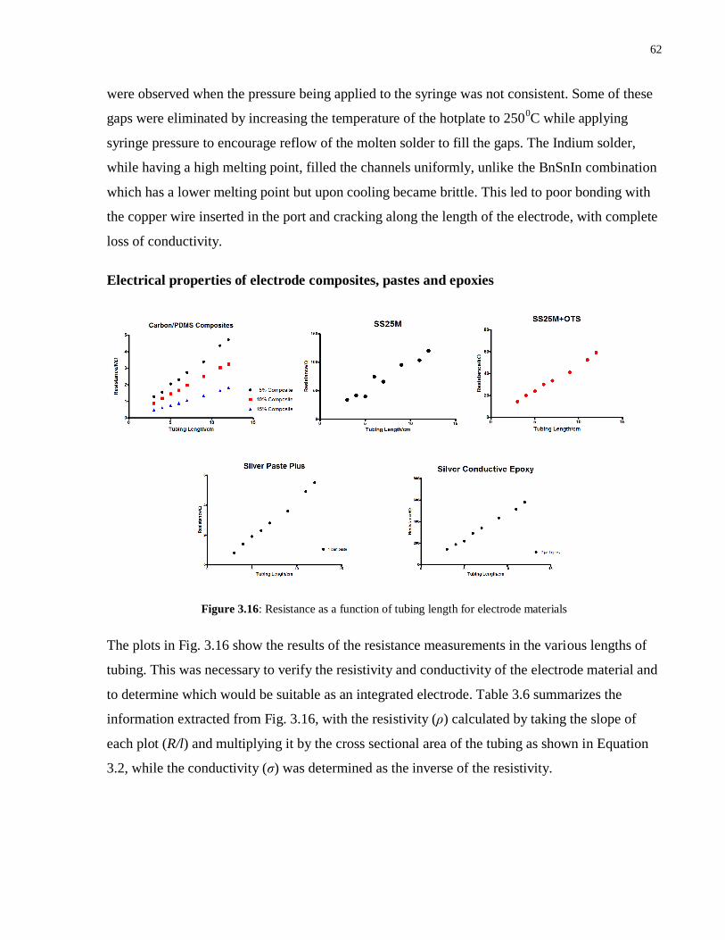
62
were observed when the pressure being applied to the syringe was not consistent. Some of these
gaps were eliminated by increasing the temperature of the hotplate to 2500C while applying
syringe pressure to encourage reflow of the molten solder to fill the gaps. The Indium solder,
while having a high melting point, filled the channels uniformly, unlike the BnSnIn combination
which has a lower melting point but upon cooling became brittle. This led to poor bonding with
the copper wire inserted in the port and cracking along the length of the electrode, with complete
loss of conductivity.
Electrical properties of electrode composites, pastes and epoxies
Figure 3.16: Resistance as a function of tubing length for electrode materials
The plots in Fig. 3.16 show the results of the resistance measurements in the various lengths of
tubing. This was necessary to verify the resistivity and conductivity of the electrode material and
to determine which would be suitable as an integrated electrode. Table 3.6 summarizes the
information extracted from Fig. 3.16, with the resistivity (ρ) calculated by taking the slope of
each plot (R/l) and multiplying it by the cross sectional area of the tubing as shown in Equation
3.2, while the conductivity (σ) was determined as the inverse of the resistivity.

63
Electrical
Property
Product/Material Name
C-
PDMS SS-25M
SS-25M
+ OMS
Silver
Paste
Plus
Silver
Conductiv
e Epoxy
Indium
Solder
Bn-In-
Sn
Solder
Manufacturer‟s
Resistivity
(ρ)/Ω·cm
NA 6 x 10⁻²
NA 3 x 10⁻⁵
3.8 x 10⁻¹
8.37 x 10⁻⁵
NA
Measured
Resistivity
(ρ)/Ω·cm
5%:
1998.2
10%:
1367.7
15%:
771.1
4.9 x 10⁻²
248 2.63 x 10⁻³
2.51 x 10⁻¹
†4.36 x 10
-3
†7.4 x 10
-2
Manufacturer‟s
Conductivity
(σ)/S·cm-1
NA 16.7 NA 3.33 x 10⁴ 2.63 1.19 x 10
4 NA
Measured
Conductivity
(σ)/S·cm-1
5%:
5.0 x 10⁻⁴
10%:
7.3 x 10⁻⁴
15%:
1.3 x 10⁻³
20 4.03 x 10⁻³
3.81 x 10² 3.98 2.29 x 10
2 13.5
Microelectrode
Resistance/Ω NA 5.78 x 10
4 24 x 10
6 2.87 x 10
3 2.69 x 10
5 4.61 x 10
3 7.95 x 10
4
† - obtained from resistance measurements of solder block
Table 3.6: Electrical properties of all conductive materials used as integrated electrodes
The table above indicates that the Silver Paste Plus single part paste had the best conductivity
and lowest resistance at the microelectrode level. However, the process of measuring the
resistance of the microelectrode often led to damages to the electrode due to the copper wire
breaking the paste matrix or compressing it in an irreparable manner. This was observed for all

64
integrated electrodes in which a paste or epoxy was used. Meanwhile, the indium solder had a
comparable electrical conductivity and microelectrode resistance, and while measurement of the
microelectrode resistance also punctured the embedded solder, the device was placed on a
hotplate at 2500C to re-melt the solder, causing reflow and fixing any damaged regions. As a
result, the indium solder was determined to be the preferred choice for the integrated electrode
material and was used for fabricate all microfluidic devices for in vitro studies.
3.3.5 Microfluidic device with integrated electrodes
Figure 3.17: Final microfluidic device with integrated solder electrodes
100µm

65
3.4 Conclusion
The work in this chapter has demonstrated the ability to improve the resolution and feature size
of structures fabricated via UV photolithography using a plastic photo mask. The minimum
feature size of 5.5µm achieved, with near straight side walls, is significantly better than those
fabricated by similar methods as reported in the literature [90] and enabled the development of a
reproducible microfluidic device capable of confining a single cell while restricting the diffusion
of analytes. Additionally, a unique integration of 3-D electrodes, close to, but not in direct
contact with the fluidic channel was also implemented through a combination of the optimized
fabrication process and injection moulding of good electrically conducting solder.

66
Chapter 4 In vitro experimental verification of plasma membrane lysis
4.1 Introduction
Verification of selective electrical lysis of the plasma membrane, while the nuclear membrane
remains intact, should be facilitated with normal and diseased cells to determine the effectiveness
of the lysis method on each type. The work in this thesis employed 3T3 rat fibroblasts as a
normal model, and 9L rat gliosarcomas as a diseased brain tumour model.
3T3 cells
Established in 1962, the name refers to “3-day transfer, inoculum 3 x 10⁵ cells”, and due to the
large volume of data available on this cell line, it has been used as a model system extensively in
experimental research. Furthermore, these adherent cells have been used repeatedly in
microfluidics and have demonstrated the ability to maintain viability in PDMS structures [91].
Electroporation of single 3T3 cells has been reported to occur with an applied electric field
strength of under 4 kV·cm-1
[92] and are typically 8-15µm in size.
9L cells
These rare, malignant form of gliomas are adherent and have sizes between 10-12µm. These
cells closely simulates glioblastoma multiform when implanted in vivo and consequently has
been used often in photodynamic therapy studies [93] and more recently in detecting cancer
stem-like cells [94]. While no literature exists on electroporation of single 9L cells, they are
typically lysed by ~1 kV·cm-1
electric fields.

67
4.2 Materials and Methods
4.2.1 Experimental set-up
Fluidic system and flow control
Common flow control features in microfluidic devices often include syringe pumps [95], on-chip
micropumps, microvalves and actuators [96, 97]. Initially for this project, an NE-1000 syringe
pump (New Era Pump Systems Inc., Wantagh, NY, USA) was used; however, the minimum
flow rate was limited to ~0.2nl·s-1
for a 1ml syringe. The total volume of the fluidic channel
between the entry port and the injector structure was ~1nl, thus only a 5s window was available
for fluid manipulation. As a result, a system relying on Bernoulli‟s principle was adopted for this
thesis. In fluid dynamics, this principle states that a change in the speed of a fluid undergoing in-
viscous flow occurs simultaneously with a change of its potential energy or its pressure [98].
Noguchi et al [99] presented a thorough analysis of flow dynamics of model particles (vesicles)
governed by a modified Poiseuille flow in microfluidic channels due to rectangular channels
compared to normal cylindrical channels in which the flow was controlled by Bernoulli‟s
principle with a height varying system. A modification to their system was implemented to allow
flow manipulation in this thesis.
The first part of the fluid control mechanism comprised a step to flush the fluidic channel
with a 3ml syringe with a 23 gauge needle attached. The needle was sheathed by Tygon flexible
plastic tubing (Cole-Parmer Inc., Montreal, QC, Canada), 60cm in length, with inner diameter
0.51mm and outer diameter 1.52mm. At the opposite end of the tubing, a 12.7mm length of
stainless steel tubing (New England Small Tube Corp., Litchfield, NH, USA) with a 0.43mm
bore and outer diameter of 0.635mm was fitted, and inserted into the fluidic entry port of the
microfluidic chip. A buffer solution containing 0.01% Pluronic (Sigma-Aldrich Ltd., Oakville,
ON, Canada) was used to fill the channel using the syringe set-up, after which the needle was
removed and submerged in a 15ml Falcon tube containing the same solution. The tube was
secured to a height varying stage controlled by a z-axis travel translation stage (Thorlabs,
Newton, NJ, USA) as shown in Fig. 4.1 initially set to an equilibrium state of zero flow. The
microfluidic chip was secured to an in-house fabricated microscope stage using a pair of metal
clamps to ensure chip stability during experiments and observations were made using an
Axiovert 200M inverted microscope with a 10X Fluar objective (Carl Zeiss, Toronto, ON,
Canada)
(a)

68
Figure 4.1: Image of flow control system
Cell preparation and fluorescent labelling of cytoplasm and nucleus
Two different cell lines were used for in vitro experiments on chip, namely 3T3 fibroblasts and
9L gliosarcoma cells. Each cell line was cultured using Dulbecco‟s Modified Eagle‟s (DME)
Medium formulation (Invitrogen Inc., Burlington, ON, Canada) containing physiological
components including vitamins, amino acids, sugars, inorganic salts and phenol red to determine
the presence of any chemical reactions within the media which may affect pH. The typical
physiological pH of cells is ~ 7.2-7.4 which produces red colour in the cell culture media;
however, a change in the pH to more basic or more acidic would be accompanied by a change in
colour. The media was also supplemented with 10% fetal bovine serum (FBS) which contains
essential growth factors aiding in stimulation of cellular growth. Antibiotics in the DME, such as
streptomyocin and penicillin, also help to prevent the growth of gram positive and gram negative
organisms which may infect or contaminate the cell culture. Cells were incubated in standard cell
culture flasks at 370C/5% CO2.
Specialized
microscope
stage Translation
Stage Translation
Stage

69
The membrane permeable dye, calcein AM (Invitrogen Inc., Burlington, ON, Canada), excited at
495nm and emits at 515nm, was used as a fluorescent marker for the cytoplasm of viable cells.
Upon entering the cell, the acetomethoxy group of the dye (Fig. 4.2) is hydrolyzed by
intracellular esterases converting the non-fluorescent calcein AM into a strong green-fluorescent
calcein. Cells were trypsinized and re-suspended (~1-2 x 10⁶ cells·ml
-1) in buffered media of pH
7.2 with phenol red free media (alpha MEM), after which 1mM of the dye was administered and
incubated for 1 hour at 370C, allowing adequate transport through the membrane and hydrolysis
in the cytoplasm.
Figure 4.2: Calcein AM molecule (C46H46N2O23) and excitation/emission spectra (Adapted from [100])
Following incubation, cells were centrifuged at 2000 rpm, the supernatant removed, and
re-suspended in clear alpha MEM. To tag the nucleus, Hoechst 33342 (Invitrogen Inc.,
Burlington, ON, Canada) was used and is excited at ~350nm and emits at 461nm (Fig. 4.3). The
dye is rendered lipophilic by its ethyl group, making it permeable to the plasma membrane, and
binds to the A-T base pairs of DNA. A concentration of 5µM of Hoechst was added to the
suspended cells and incubated for at least 30 minutes at 370C to allow diffusion of the dye. After
this incubation period, cells were again centrifuged at 2000 rpm, the supernatant removed and a
final re-suspension in clear alpha MEM was carried out.

70
Figure 4.3: Hoechst 333342 molecule (C27H37Cl3N6O4) and excitation/emission spectra (Adapted from [100])
On the microfluidic chip, the cell reservoir, located at the opposite end of the fluidic
channel to the control port (Fig. 3.1), was filled with 50µl (~0.5 – 1 x 10⁵ cells) of the cell
suspension and the height of these reservoirs represented the zero potential. Fine adjustments
were made to the z-stage, varying the Falcon tube holder by 1mm increments to create a pressure
gradient between the reservoir and the fluidic control port, permitting adequate control of the
flow, and allowing a single cell to be stopped completely in the region of the injector structure,
eliminating mechanical stress during lysis. While optical tweezers were available to facilitate
single cell selection and transport from the cell reservoir to the injector structure, the distance of
~3mm would have required too much time.
Electronic set-up for electrical lysis
According to simulations in Chapter 2 Section 2.3.2, an electric field in the range 4.507-
4.532kV·cm-1
is generated when a potential difference of 32V is applied across the electrodes,
thus to examine the effect of varying the magnitude of the electric field on cell lysis, a DC power
supply capable of achieving a range of at least 0 – 50V was selected. Additionally, a function
generator or arbitrary waveform generator was needed to create a pulsed DC source to
effectively induce electroporation as explained in Chapter 2, Section 2.1.2 and an Agilent
33220A (Agilent Technologies Inc., Mississauga, ON, Canada) was used for this requirement.
Since this function generator has a maximum peak voltage output of 10V, an external DC power
supply was required to generate a DC offset and produce a new maximum peak voltage of at
least 32V. This was achieved using an Agilent HP 6209B DC power supply (Agilent
Technologies Inc., Mississauga, ON, Canada) with a voltage output range of 0 – 320V,

71
connected in series as shown in Fig. 4.4, to the function generator and the load, in this case, the
micro electrodes, using a method suggested by Agilent Technologies [101]. The electrical
connection to the copper wire electrode contacts was made using a BNC cable modified with a
pair of mini grippers (Mouser Electronics, Mansfield, TX, USA) at one end while the opposite
end was connected to the function generator.
Figure 4.4: Circuit diagram of function generator with external DC offset
4.2.2 Visual monitoring of electric field induced cell lysis
Quantification of photobleaching effects
With the electrical components connected, the translation stage was adjusted to load a single cell
into the injector structure region, and nuclear fluorescence of Hoechst was obtained by excitation
with a mercury source (BH2-RFL-T3, Olympus, Japan) filtered by an ET-DAPI filter set
(Chroma Technology Corp., Bellows Falls, VT, USA). If fluorescence was observed through the
same filter set, a video of the nuclear fluorescence of the cell was captured at 15fps for 30s using
the CoolSNAP Pro camera and ImagePro Plus software was employed to determine the effects of
photobleaching over the duration of the cell lysis experiments. If the nucleus exhibited no
VGEN = Regular voltage of function generator
VOUT = Final output voltage
Position A – Output BNC (front)
Position B – Modulation In BNC (back)
72
fluorescence, the flow was adjusted to steer the cell through the funnel in the injector structure
and another cell was loaded. Following Hoechst imaging, the cell was allowed to pass through
the injector structure, and another cell was loaded. Calcein was excited and monitored using the
same light source with a FITC-EGFP filter set (Chroma Technology Corp., Bellows Falls, VT,
USA). A video was captured of the cytoplasmic fluorescence at 15fps for 180s after which the
cell was flushed through the microchannel. While this experiment was intended to determine the
effects of photobleaching, it also serves as a control case in which cells were observed in the
absence of an electric field.
Electrical lysis of plasma membrane
The effects of electrical lysis of the plasma membrane, without hindrance to the nuclear
membrane was investigated by loading a single cell into the injector structure, and positioning it
in place at the funnel, described in Chapter 3 Section 3.2.1. Still images were collected of the
cell, and its diameter was determined using ImagePro Plus. A fluorescent image of the nuclear
stain was obtained and after changing filters to FITC-EGFP, a video of the cytoplasmic
fluorescence was recorded at 15fps for 4-5s, with the function generator turned on 0.6s after
recording had begun. The pulse duration was set to 100µs while the output voltage was 32V and
the remained on for the entire duration of the recording process. Immediately after the function
generator was turned off, the nuclear fluorescence was again imaged to determine the integrity of
the nucleus following the application of an electric field. This process was repeated for both 3T3
and 9L cells using 3 cells per microfluidic chip for 3 different chips, totalling 9 cells for each cell
line.
Additionally, a small number of cells from each cell line were subjected to lower (4 –
20V) and higher voltages (36 – 40V) to observe the effect on both the plasma membrane and
nucleus.
4.2.3 Data analysis
While the fluorescent images and videos obtained for the photobleaching of Hoechst offer a
qualitative perspective, a more quantitative analysis was required to determine the change of
intensity as a function of time. The videos were decompiled into individual frames using a video
processing utility, VirtualDub (VirtualDub.org, USA), and at frames corresponding to a 3s

73
interval the profile of the fluorescent intensity was plotted as a function of position along the y-
axis. Since the funnel of the injector structure allows cell confinement and restricts diffusion of
cellular content laterally along the x and z axes of the channel, the fluorescent profile along the
y-axis of the channel was investigated as illustrated in Fig. 4.5. ImageJ (National Institute of
Health, USA) was used to perform a background subtraction on each image and to extract the
intensity profile. This was repeated for the photobleaching effects of calcein, with the fluorescent
intensity profile extracted frames corresponding to 10s intervals.
Figure 4.5: Illustration of direction of fluorescent profile analysis
The images obtained of the nuclear staining before and after electrical lysis were
analysed in a manner similar to that described previously, however only at two time points, 0s
and 6s. Meanwhile, the analysis of the diffusion of cytoplasmic staining from within the cell was
performed similarly, with y-profiles obtained at time intervals of 0.2s and the FWHM of each
profile was determined as a function of time, permitting extraction of the diffusion rate of each
cell to be obtained.
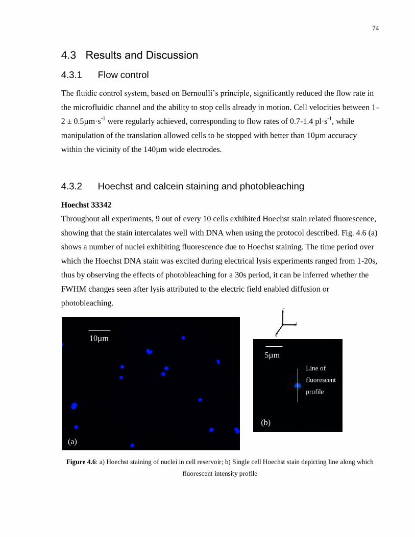
74
4.3 Results and Discussion
4.3.1 Flow control
The fluidic control system, based on Bernoulli‟s principle, significantly reduced the flow rate in
the microfluidic channel and the ability to stop cells already in motion. Cell velocities between 1-
2 ± 0.5µm·s-1
were regularly achieved, corresponding to flow rates of 0.7-1.4 pl·s-1
, while
manipulation of the translation allowed cells to be stopped with better than 10µm accuracy
within the vicinity of the 140µm wide electrodes.
4.3.2 Hoechst and calcein staining and photobleaching
Hoechst 33342
Throughout all experiments, 9 out of every 10 cells exhibited Hoechst stain related fluorescence,
showing that the stain intercalates well with DNA when using the protocol described. Fig. 4.6 (a)
shows a number of nuclei exhibiting fluorescence due to Hoechst staining. The time period over
which the Hoechst DNA stain was excited during electrical lysis experiments ranged from 1-20s,
thus by observing the effects of photobleaching for a 30s period, it can be inferred whether the
FWHM changes seen after lysis attributed to the electric field enabled diffusion or
photobleaching.
Figure 4.6: a) Hoechst staining of nuclei in cell reservoir; b) Single cell Hoechst stain depicting line along which
fluorescent intensity profile
10µm
5µm
(a)
(b)
Line of
fluorescent
profile

75
Figure 4.7: a) Hoechst fluorescent intensity profile as a function of position for various time points; b) Area under
each intensity peak as a function of time
While there appears to be movement of the nucleus along the y-axis of the channel (Fig.4.7 (a)),
there is no significant photobleaching, as evidenced by a slope of -0.06364 ± 0.2664 s-1
for a line
of best fit to the data presented in Fig. 4.7 (b) as the 95% confidence interval contains zero. Thus
it can be concluded that for the time periods for which the Hoechst stain is excited during lysis
experiments (1-20s), photobleaching effects are negligible.
Calcein AM
The staining of the cytoplasm exhibited slightly lower efficacy compared to the nuclear staining,
with approximately 8 in 10 exhibiting calcein fluorescence (Fig. 4.8 (a)). This may have been
due to inadequate hydrolysis of the dye molecules by intracellular esterases. The extended time
duration over which photobleaching of calcein was observed was required since this dye was
excited for up to 90s during set-up and electrical lysis experiments.
(a) (b)

76
(a) (b)
Figure 4.8: a) Calcein staining of cytoplasm in cell reservoir; b) Single cell calcein stain depicting line along which
fluorescent intensity profile
Figure 4.9: a) Calcein fluorescent intensity profile as a function of position for various time points; b) Area under
each intensity peak as a function of time
The fluorescent intensity profiles of calcein at 60s intervals exhibit a change in peak intensity
(Fig. 4.9 (a)), resulting in a change of the total fluorescent intensity, confirmed in Fig. 4.9 (b). A
line of best fit yields a slope of -0.4179 ± 0.09572 s-1
, supporting photobleaching; however, for
20µm
20µm
Line of
fluorescent
profile
(a)
(b)
(a) (b)

77
the duration of electrical lysis experiments, these effects were considered insignificant as the
overall change of intensity over a 180s interval is only 2.9% as extracted from Fig. 4.9 (b).
4.3.3 Electrical lysis of 3T3 and 9L plasma membranes
3T3 cells
The average diameter of 3T3 cells was determined to be 10 ± 2µm and results indicated that at an
applied voltage of 32V, with 100µs pulse duration, producing an electric field in the range 4.507
– 4.532kVcm-1
, electrical lysis of the plasma membrane was evident. While video of the
cytoplasmic fluorescence provided visual evidence of this as shown in Fig. 4.10, an analysis of
the fluorescent intensity profile offered quantification of the process.
Figure 4.10: a) Fluorescent image of cytoplasm, a) before lysis, 0s; b) after lysis, 4s
Fluorescent intensity profiles extracted from videos of the electrical lysis process at 0.2s
intervals for 3 different cells from the same microfluidic chip is shown in Fig. 4.11 (left). Each
cell exhibits a decrease of maximum intensity and a broadening of the peak, both as a function of
time, and represents the diffusion of the calcium ions from the cytoplasm along the y-axis of the
microfluidic channel. Meanwhile, the corresponding change of the nuclei of each cell, as
represented by the Hoechst stain, from the start to finish of lysis can be seen in Fig. 4.11 (right).
The shift of the Hoechst intensity profile in some plots along the position axis is attributed to
10µm 10µm
(a) (b)

78
motion of the nuclei along the y-axis of the microfluidic channel following lysis. Compared to
the Hoechst stain, the calcein stain appears to exhibit weaker fluorescence, highlighted by the
difference in peak intensities between the two. While this was not evident in cells in all
microfluidic chips, this outcome can be attributed to poor hydrolysis of calcein AM by
intracellular esterases.
Figure 4.11: Fluorescent intensity profile as a function of position for 3 different 3T3 cells on the same chip
showing cytoplasmic (left column) and nucleic (right column) changes over time between t = 0s and t = 6s
Calcein Hoechst
Cell 1
Cell 2
Cell 3
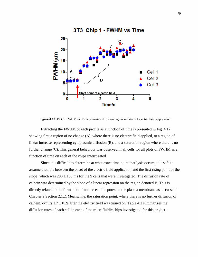
79
Figure 4.12: Plot of FWHM vs. Time, showing diffusion region and start of electric field application
Extracting the FWHM of each profile as a function of time is presented in Fig. 4.12,
showing first a region of no change (A), where there is no electric field applied, to a region of
linear increase representing cytoplasmic diffusion (B), and a saturation region where there is no
further change (C). This general behaviour was observed in all cells for all plots of FWHM as a
function of time on each of the chips interrogated.
Since it is difficult to determine at what exact time point that lysis occurs, it is safe to
assume that it is between the onset of the electric field application and the first rising point of the
slope, which was 200 ± 100 ms for the 9 cells that were investigated. The diffusion rate of
calcein was determined by the slope of a linear regression on the region denoted B. This is
directly related to the formation of non resealable pores on the plasma membrane as discussed in
Chapter 2 Section 2.1.2. Meanwhile, the saturation point, where there is no further diffusion of
calcein, occurs 1.7 ± 0.2s after the electric field was turned on. Table 4.1 summarizes the
diffusion rates of each cell in each of the microfluidic chips investigated for this project.
A
B
C
Start point of electric field

80
Property
Chip 1 Chip 2 Chip 3
Cell 1 Cell 2 Cell 3 Cell1 Cell 2 Cell 3 Cell 1 Cell 2 Cell 3
Diffusion
Rate
(µm·s-1
)
5.712 ±
0.7979
6.062 ±
0.9183
5.364 ±
0.8837
4.061 ±
0.1350
3.665 ±
0.1560
4.522 ±
0.3022
5.316±
0.4791
5.790±
0.6033
5.703±
0.6786
Total
Fluorescent
Intensity of
Hoechst
Stain before
lysis
508.8 478.1 702.5 645.3 711.2 703.0 700.5 708.2 703.9
Total
Fluorescent
Intensity of
Hoechst
Stain after
lysis
498.8 463.1 681.9 633.1 690.8 689.9 689.6 692.0 681.5
% Change in
Hoechst
Fluorescence
2.0 3.1 2.9 1.9 2.9 1.9 1.6 2.3 3.2
Table 4.1: Summary of diffusion rates and fluorescent intensity data for nine 3T3 cells
The average diffusion rate was 5.133 ± 0.277 µm·s-1
, while the FWHM became
asymptotic at 20.23 ± 2.15 µm·s-1
after the saturation point was reached. This supports the
hypothesis that within the experimental time interval, cells undergo significant rupturing of the
plasma membrane due to electrical lysis, creating permanent pores that are not re-sealable. As a
result, the calcein was expelled and diffused along the y-axis of the fluidic channel although
there was no continuous flow present, until a saturation point was reached. Meanwhile, the
average loss of Hoechst fluorescent intensity was 2.4% between the start of the electrical lysis

81
process and the end of the observed saturation region. This suggests that while the plasma
membrane was ruptured, evident by the expulsion of calcein from the cell, the nuclei remained
largely intact with no diffusion of the Hoechst stain observed.
9L cell
The disease model 9L cells had an average diameter of 8.5 ± 2µm and exhibited signs of
membrane lysis when a voltage of 32V, with 100µs pulse duration, producing an electric field in
the range 4.507 – 4.532kVcm-1
. Fig. 4.13 (left) shows the results of the fluorescent intensity
profiles for 3 different cells on a single microfluidic device via analysis of video frames
extracted at 0.2s intervals.

82
Figure 4.13: Fluorescent intensity profile as a function of position for 3 different 9L cells on the same chip showing
cytoplasmic (left column) and nucleic (right column) changes over time between t = 0s and t = 6s
Calcein Hoechst
Cell 1
Cell 2
Cell 3

83
The plots indicate that while the profiles of the fluorescent intensity of calcein in the
cytoplasm exhibit peak broadening and a decrease in maximum intensity, both as a function of
time, the general Gaussian appearance of the profiles remains intact. This is possibly due to
incomplete poration of the plasma membrane, resulting in higher retention of calcein than that
observed in 3T3 cells. Fig. 4.13 (right) shows that over the duration of electrical lysis, the
fluorescent intensity profiles of Hoechst in the nuclei maintain their shape, with miniscule shifts
along the position axis, representing the movement of the nuclei along the y-axis of the channel.
The FWHM of each profile at 0.2s intervals (Fig. 4.14) shows an initial region, before
application of the electric field, A, region of diffusion, B, and saturation region, C. Fluorescent
intensity profiles and FWHM plots of the nine 9L cells investigated on 3 different microfluidic
chips were all observed to adhere to a similar pattern.
Figure 4.14: Plot of FWHM vs. Time, showing diffusion region and start of electric field application
While it is again difficult to determine the exact time of lysis, Fig. 4.14 suggests that lysis
occurs fractionally earlier in 9L cells than was observed for 3T3 cells, which was about 150 ±
100 ms after the application of the electric field for the 9 cells that were investigated. The
diffusion rate of calcein was determined by the same methods used for 3T3 analysis and was
found to reach saturation 2.3 ± 0.2s after application of the electric field. Table 4.2 summarizes
B
A
Start point of electric field
C
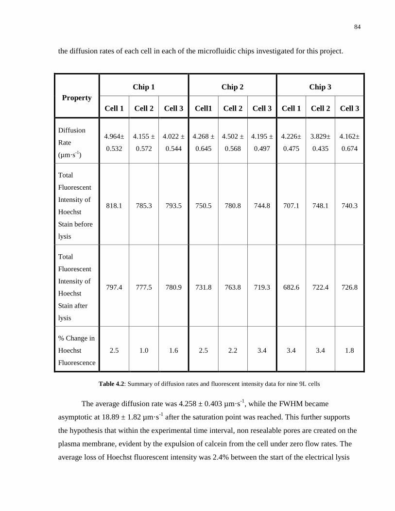
84
the diffusion rates of each cell in each of the microfluidic chips investigated for this project.
Property
Chip 1 Chip 2 Chip 3
Cell 1 Cell 2 Cell 3 Cell1 Cell 2 Cell 3 Cell 1 Cell 2 Cell 3
Diffusion
Rate
(µm·s-1
)
4.964±
0.532
4.155 ±
0.572
4.022 ±
0.544
4.268 ±
0.645
4.502 ±
0.568
4.195 ±
0.497
4.226±
0.475
3.829±
0.435
4.162±
0.674
Total
Fluorescent
Intensity of
Hoechst
Stain before
lysis
818.1 785.3 793.5 750.5 780.8 744.8 707.1 748.1 740.3
Total
Fluorescent
Intensity of
Hoechst
Stain after
lysis
797.4 777.5 780.9 731.8 763.8 719.3 682.6 722.4 726.8
% Change in
Hoechst
Fluorescence
2.5 1.0 1.6 2.5 2.2 3.4 3.4 3.4 1.8
Table 4.2: Summary of diffusion rates and fluorescent intensity data for nine 9L cells
The average diffusion rate was 4.258 ± 0.403 µm·s-1
, while the FWHM became
asymptotic at 18.89 ± 1.82 µm·s-1
after the saturation point was reached. This further supports
the hypothesis that within the experimental time interval, non resealable pores are created on the
plasma membrane, evident by the expulsion of calcein from the cell under zero flow rates. The
average loss of Hoechst fluorescent intensity was 2.4% between the start of the electrical lysis

85
process and the end of the observed saturation region, giving further evidence of nuclear
membrane intactness.
4.3.4 Variation of diffusion rate due to electric field
Observations and analysis of 3T3 cells under the influence of electric fields expected to be too
low to induce lysis, and fields higher than that used for all other work in this thesis, were
performed in the same manner as described above for a fixed field strength. The values of the
mean electric field were obtained from simulations in Chapter 2, given in Table 2.1, while the
diffusion rates were averaged for 3 cells at each applied electric field. Fig. 4.15 illustrates that at
low field strengths, there appears to be no diffusion of calcein, while the small amounts shown
may be attributed to electroporation. At higher field strengths, the diffusion rate increases
linearly with the applied electric field; however, due to limitations of the electronic set up, fields
in excess of 10kV·cm-1
were not investigated. It should be expected that at fields at and above
this value, the entire cell, with a large majority of its organelles, including the nucleus, would be
lysed, leading to a saturation point in the diffusion rate.
Figure 4.15: Dependency of diffusion rate of calcein on mean electric field strength for 3T3 cells

86
4.4 Conclusion
Both models demonstrated the expulsion of calcein labelled molecules from the cell upon
application of the electric field, and since there was no flow present in the fluidic channel during
lysis, the diffusion of calcein along the y-axis of the channel could be attributed to a pressure
gradient existing between the inner and outer regions of the cell. Comparison of Fig 4.11 and
Fig. 4.13, along with experimental data for other microfluidic chips, suggest that while 3T3 cells
appear to expel a significant amount of calcein, evident by the loss defined peaks while the
FWHM increases, calcein in 9L cells maintain a distinct Gaussian profile, suggesting that some
of the calcein is still held within the lysed cell. This is most likely due to inadequate pore
creation on the surface of the plasma membrane. Intactness of the nuclear membrane was evident
in both types of cells due to the retention of > 95% of the Hoechst stain within their nuclei.

87
Chapter 5 Summary and Future Work
5.1 Summary
The goal of this thesis was to develop a microfluidic device with integrated electrodes, capable
of performing selective electrical lysis of the plasma membrane of single cells, while leaving the
nuclear membrane intact. An understanding of the mechanism of irreversible electroporation and
the electrical requirements to achieve lysis of only the plasma membrane provided the basis to
achieve this goal.
Due to their variation in size and membrane charging time, the electric field required to
surpass a threshold transmembrane potential or transorganelle potential which mediates lysis, is
significantly different for plasma membranes and those of intracellular organelles, with the latter
requiring a much high electric field to induce lysis. While this concept has been theoretically
investigated [28], there is limited experimental evidence, especially with respect to single cells.
Microfluidic devices afford the opportunity to investigate single cells, while restricting the
aberrant diffusion of cell contents, thus enabling the ability to determine whether selective lysis
is effective.
Performing electrical lysis of single cells within a microfluidic device has previously
been investigated [28, 51]; however, other systems lack the ability to separate the electrode from
either the extracellular media or the cell itself, which often results in thermal or mechanical
damage to cells coming into contact with electrodes. Additionally, due to the geometrical and
electrical limitations of these devices, cells are usually lysed in an uncontrolled manner, with no
regard for selectivity, and cell contents are diffused throughout microchannels due to lack of
cellular confinement, making downstream analysis difficult. The microfluidic device that we
have presented, addresses many of the shortcomings of previous systems, while providing
evidence of selective lysis of the plasma membrane and negating thermal damage to the cell.

88
5.2 Contributions and perspectives
5.2.1 Microfluidic device fabrication for single cell electrical lysis
The current available microfluidic techniques to perform single cell electrical lysis can be
improved by geometric considerations and positioning of electrodes. In the fabrication of the
microfluidic device used in this project, the following contributions were made:
1. Improvement on UV photolithography of SU-8 using a plastic photo mask to
produce aspect ratios of 1:3 and greater, comparable to published reports [80, 102].
The use of glycerol as an index matching and gap compensating media,
previously demonstrated by other groups, coupled with high quality photo masks,
enabled minimum feature widths of 5.5 ± 1.5µm with 3% magnification from
mask to SU-8. However, feature widths can be significantly minimized by using
quartz-chrome masks, which are typically manufactured by laser etching, and
does not require any compensating media.
2. Development of geometrical design which allows integrated electrodes. By taking
advantage of the improved width resolution, a microfluidic chip was designed to
enable electrodes to be offset in the x-axis from fluidic channels and buffered by
PDMS walls to prevent electrode – cell interactions.
3. Integration of In microelectrodes in close proximity to fluidic channel. While Siegel
et al [87] demonstrated the ability to integrate molten solder into PDMS to fabricate
electromagnets, this method was never investigated for microelectrodes for electrical
lysis. Due to the tediousness and time required to work with molten solder at ~
2000C, alternative electrode material should be explored to speed up fabrication time
of the microfluidic system.
89
5.2.2 Selective electrical lysis of plasma membrane of single cells
Theoretical models have shown that with the application of either a DC or AC electric field,
having specific electrical parameters as discussed in Chapter 2, it is possible to lyse the plasma
membrane of a cell, while the membranes of intracellular organelles remain intact.
Experimentally, this theory has not been thoroughly investigated, especially in microfluidics,
while other lysis methods have demonstrated this ability. The following contributions and
observations were made through in vitro studies in this project:
1. Demonstrated the ability to perform selective electrical lysis of the plasma membrane
of single 3T3 and 9L cells, supported by pre and post lysis analysis of the
fluorescently labelled cytoplasm and nuclei. The novel approach of integrating
microelectrodes in close proximity to cells, without coming into contact with cells,
allowed the plasma membrane to be electrically lysed, with visual evidence of the
cytoplasm exiting the cell, while the nuclei remained intact throughout the process.
However, further labelling of other intracellular organelles of interest and upstream
biochemical analysis would be necessary to further refine and validate the lysis
parameters.
2. As a result of the confinement provided by the injector structure, and the theorized
uniform pore creation on the surface of the plasma membrane, relatively low
diffusion rates were achieved, which is desirable for downstream analysis by capillary
electrophoresis in combination with LIF.
5.3 Future Work
5.3.1 Engineering and fabrication aspects
While this project demonstrated the ability to perform selective lysis of the plasma membrane,
the injector structure is incapable of efficiently separating the cytoplasm from the nuclei. The
narrow funnel of the injector structure tapers to a 5.5µm channel; however, a typical nuclei is
~2µm, thus under the influence of flow, would be inseparable from the cytoplasm and other
nuclei. Micro pillars etched into cured SU-8 by excimer laser ablation [103] is one option to
fabricate a sieve like region within the injector structure as an alternative to having an expensive

90
quartz-chrome mask. This would allow the cytoplasm to be separated from the nuclei, and
depending on the spacing of the pillars, can also separate smaller organelles, such as the
mitochondria, from the cytoplasm.
A new photo mask design is necessary to create a new microfluidic device which will
permit high throughput analysis by parallelizing the selective lysis process, similar to parallel
systems demonstrated by Munce et al [24]. Prior to designing a new mask, an estimation of the
minimum distance between fluidic channels, and the effect of electric fields on parallel systems
would be necessary, possibly using COMSOL simulations. The design shown in Fig. 5.2 shows a
parallel system; however, the distances between channels have not been optimized as constraints
provided by LIF detection system will also have to be considered.
The use of In molten solder, while yielding high electrically conductive microelectrodes,
is often tedious and time consuming due to the injection process. In instances where the electrode
filling channels are not properly silanized, the solder has been observed to not fill the channel
entirely, while excess solder on the PDMS surface can sometimes result in darkening of the
PDMS. Additionally, solid solder particulates have been observed to contaminate the cell
reservoir, leading to clogging of the fluidic channel. Upon the completion of this project, a liquid
metal alloy, eutectic GaIn, with melting point ~ 15.50C, was found in the literature [104] to form
stable structures in microchannels, and should be further investigated as an alternative electrode
material. The alloy reportedly fills channels without the need for pre-treatment and can be
removed and re-used in other electrodes, while filled channels can be stored at 40C.
5.3.2 Integration of components
The flow control system used in this project was sufficient to allow a randomized, single cell to
be selected from the cell reservoir; however, optimization of the optical tweezers available as
part of this program, could allow a specific cell to be selected and transported to the injector
structure. Currently, the force produced by the tweezers is not adequate to move a cell over a
large distance, with cells becoming dislodged from the optical trap when coming into contact
with channel walls or other cells.
With the parallelization of the injector structures and electrodes, optical tweezers would
again be inadequate to quickly load multiple cells, thus the flow system can again be employed,
or alternatively, the use of syringe pumps capable of producing the necessary flow rates.

91
However, loading multiple cells flowing along a channel into separate injector structures would
be difficult to control by flow alone, thus optical waveguides, as shown in Fig. 5.2, also
developed as part of this program, would be required to load cells into injector structures for
selective lysis.
Figure 5.1: Parallelized system with multiple electrode filling ports
The information content available through fluorescent analysis, while sufficient to give
evidence of selective lysis, is limited when greater detail is required. Capillary electrophoresis
would provide additional biochemical information from lysed cells and, with new microfluidic
designs and possibly the use of microvalves, can be integrated along with the current lysis
system. Channel lengths and widths will need to be optimized to produce acceptable
electrophoretic resolution as the narrow 5.5µm channel following the injector structure would
result in poor separation of analytes, thus poor resolution. Initial work performed by Pelzer [105]
on the development of a fibre array for LIF detection, specifically for parallel channels, have
shown promising results.
200µm

92
5.3.3 Selective lysis by AC electric field
An electric field generated by a DC source was able to selectively lyse the plasma membrane;
however, as discussed in Chapter 2, to sequentially lyse the membrane, nucleus and other
intracellular organelles, AC fields of varying applied frequencies would be required.
Additionally, an AC field with long pulse duration is capable of generating heat and possibly
inducing denaturation of organelles and lipids if required for future lysis steps.
5.3.4 Multiple fluorescent staining
Evidence of cytoplasmic diffusion and nucleic intactness, following selective membrane lysis,
was available by observing calcein and Hoechst fluorescence for the cytoplasm and nucleus
respectively. However, to determine the effects of the lysing electric field on other intracellular
organelles, such as the mitochondria, additional fluorescent labelling would be required, while
staining of the plasma membrane would enable observation of the membrane integrity post lysis.
Initial triple staining of the cytoplasm with calcein, nucleus with Hoechst and mitochondria with
Mitotracker Red (Sigma-Aldrich Ltd., Oakville, ON, Canada) has shown promising results (Fig
5.2 (a)), while staining of the plasma membrane with Rhodamine B chloride-R18 (Sigma-
Aldrich Ltd., Oakville, ON, Canada) instead of the mitochondria can be improved as the stain
appeared to enter the cytoplasm of most cells (Fig. 5.3 (b)).
Figure 5.2: (a) Staining of nucleus with Hoechst and mitochondria with Mitotracker Red; (b) Triple staining of
cytoplasm (Calcein AM), nucleus (Hoechst) and plasma membrane (R18)
(a) (b)
3µm 8µm
10µm 10µm
(a) (b)

93
Bibliography
[1] D. Cohen, J. Dickerson, C. Whitmore et al., “Chemical Cytometry: Fluorescence-Based
Single-Cell Analysis,” Annual Review of Analytical Chemistry, 1( ), pp. 165-190, 2008.
[2] C. P. Hickman, L. Roberts, and A. Larson. "The Eukaryotic Cell," April 26, 2010;
http://hyperphysics.phy-astr.gsu.edu/hbase/biology/cell.html.
[3] J. C. Kendrew, G. Bodo, H. M. Dintzis et al., “A Three-Dimensional Model of the
Myoglobin Molecule Obtained by X-Ray Analysis,” Nature, 181(4610), pp. 662-666,
1958.
[4] K. Tanaka, H. Waki, Y. Ido et al., “Protein and polymer analyses up to m/z 100 000 by
laser ionization time-of-flight mass spectrometry,” Rapid Commun. Mass Spectrom, 2(8),
pp. 151–153, 1988.
[5] K. Hu, H. Ahmadzadeh, and S. Krylov, “Asymmetry between sister cells in a cancer cell
line revealed by chemical cytometry,” Analytical Chemistry, 76(13), pp. 3864-3866,
2004.
[6] D. Di Carlo, and L. Lee, “Dynamic single-cell analysis for quantitative biology,”
Analytical Chemistry, 78(23), pp. 7918, 2006.
[7] G. Brady, “Expression profiling of single mammalian cells-small is beautiful,” Yeast,
17(3), pp. 211-217, 2000.
[8] J. Dick, “Breast cancer stem cells revealed,” Proceedings of the National Academy of
Sciences, 100(7), pp. 3547, 2003.
[9] A. Schmid, H. Kortmann, P. Dittrich et al., “Chemical and biological single cell
analysis,” Current Opinion in Biotechnology, 1( ), pp. 165-190, 2008.
[10] F. Kamme, R. Salunga, J. Yu et al., “Single-cell microarray analysis in hippocampus
CA1: demonstration and validation of cellular heterogeneity,” Journal of Neuroscience,
23(9), pp. 3607, 2003.
[11] L. P. Lee, and D. Di Carlo, "Single Cell Analysis for Quantitative Systems Biology,"
Single Cell Analysis - Technologies and Applications, D. Anselmetti, ed., pp. 135-158,
Weinheim, Germany: Wiley-Blackwell, 2009.
[12] C. V. Rao, D. M. Wolf, and A. P. Arkin, “Control, exploitation and tolerance of
intracellular noise,” Nature, 420(6912), pp. 231-237, 2002.
[13] E. A. Arriaga, "Single Cell Heterogeneity," Single Cell Analysis - Technologies and
Applications, D. Anselmetti, ed., pp. 223-234, Weinheim, Germany: Wiley-Blackwell,
2009.
94
[14] H. Yan, B. Zhang, and H. Wu, “Chemical cytometry on microfluidic chips,”
Electrophoresis, 29(9), pp. 1775-1786, 2008.
[15] J. Lichtman, and J. Conchello, “Fluorescence microscopy,” Nature Methods, 2(12), pp.
910, 2005.
[16] G. Helmlinger, M. Endo, N. Ferrara et al., “Growth factors: Formation of endothelial cell
networks,” Nature, 405(6783), pp. 139-141, 2000.
[17] R. Yuste, “Fluorescence microscopy today,” Nature Methods, 2(12), pp. 902-904, 2005.
[18] R. Schultz, T. Nielsen, J. Zavaleta et al., “Hyperspectral imaging: a novel approach for
microscopic analysis,” Cytometry, 43(4), pp. 239-247, 2001.
[19] L. Borland, S. Kottegoda, K. Phillips et al., “Chemical analysis of single cells,” Annual
Review of Analytical Chemistry, 1( ), pp. 191-227, 2008.
[20] X. Huang, M. Quesada, and R. Mathies, “DNA sequencing using capillary array
electrophoresis,” Analytical Chemistry, 64(18), pp. 2149-2154, 1992.
[21] D. Michels, S. Hu, R. Schoenherr et al., “Fully automated two-dimensional capillary
electrophoresis for high sensitivity protein analysis,” Molecular & Cellular Proteomics,
1(1), pp. 69-74, 2002.
[22] G. Whitesides, “The origins and the future of microfluidics,” Nature, 442(27), pp. 368-
373, 2006.
[23] D. Irimia, R. Tompkins, and M. Toner, “Single-cell chemical lysis in picoliter-scale
closed volumes using a microfabricated device,” Analytical Chemistry, 76(20), pp. 6137-
6143, 2004.
[24] N. Munce, J. Li, P. Herman et al., “Microfabricated system for parallel single-cell
capillary electrophoresis,” Analytical Chemistry, 76(17), pp. 4983-4989, 2004.
[25] X. Hu, P. Bessette, J. Qian et al., “Marker-specific sorting of rare cells using
dielectrophoresis,” Proceedings of the National Academy of Sciences, 102(44), pp.
15757, 2005.
[26] M. He, J. Edgar, G. Jeffries et al., “Selective encapsulation of single cells and subcellular
organelles into picoliter-and femtoliter-volume droplets,” Analytical Chemistry, 77(6),
pp. 1539-1544, 2005.
[27] A. Valero, J. Post, J. Nieuwkasteele et al., “Gene transfer and protein dynamics in stem
cells using single cell electroporation in a microfluidic device,” Lab on a Chip, 8(1), pp.
62-67, 2008.
[28] H. Lu, M. Schmidt, and K. Jensen, “A microfluidic electroporation device for cell lysis,”
Lab on a Chip, 5(1), pp. 23-29, 2005.

95
[29] J. Godin, C. Chen, S. Cho et al., “Microfluidics and photonics for Bio-System-on-a-Chip:
A review of advancements in technology towards a microfluidic flow cytometry chip,”
Journal of Biophotonics, 1(5), pp. 355, 2008.
[30] D. Huh, W. Gu, Y. Kamotani et al., “Review: Microfluidics for flow cytometric analysis
of cells and particles,” Physiological Measurement, 26( ), pp. R73-R98, 2005.
[31] W. Huang, F. Ai, Z. Wang et al., “Recent advances in single-cell analysis using capillary
electrophoresis and microfluidic devices,” Journal of Chromatography B, 866(1-2), pp.
104-122, 2008.
[32] B. Huang, H. Wu, D. Bhaya et al., “Counting low-copy number proteins in a single cell,”
Science, 315(5808), pp. 81, 2007.
[33] R. Joshi, and K. Schoenbach, “Electroporation dynamics in biological cells subjected to
ultrafast electrical pulses: a numerical simulation study,” Physical review E, 62(1), pp.
1025-1033, 2000.
[34] J. Weaver, “Electroporation of biological membranes from multicellular to nano scales,”
IEEE Transactions on Dielectrics and Electrical Insulation, 10(5), pp. 754-768, 2003.
[35] S. Ho, and G. Mittal, “Electroporation of cell membranes: a review,” Critical reviews in
biotechnology, 16(4), pp. 349-362, 1996.
[36] H. Tien, and A. Ottova, “The bilayer lipid membrane (BLM) under electrical fields,”
IEEE Transactions on Dielectrics and Electrical Insulation, 10(5), pp. 717-727, 2003.
[37] M. Davidson. "Plasma Membrane," April 7, 2010;
http://micro.magnet.fsu.edu/cells/plasmamembrane/plasmamembrane.html.
[38] J. Weaver, K. Powell, R. Mintzer et al., “The electrical capacitance of bilayer
membranes:: The contribution of transient aqueous pores,” Bioelectrochemistry and
Bioenergetics, 12(3-4), pp. 393-404, 1984.
[39] J. Weaver, and Y. Chizmadzhev, “Theory of electroporation: a review,”
Bioelectrochemistry and Bioenergetics, 41(2), pp. 135-160, 1996.
[40] C. Grosse, and H. Schwan, “Cellular membrane potentials induced by alternating fields,”
Biophysical Journal, 63(6), pp. 1632-1642, 1992.
[41] W. Krassowska, and P. Filev, “Modeling electroporation in a single cell,” Biophysical
Journal, 92(2), pp. 404-417, 2007.
[42] M. Prausnitz, V. Bose, R. Langer et al., “Electroporation of mammalian skin: a
mechanism to enhance transdermal drug delivery,” Proceedings of the National Academy
of Sciences, 90(22), pp. 10504, 1993.
[43] H. Wang, and C. Lu, “Electroporation of mammalian cells in a microfluidic channel with
geometric variation,” Analytical Chemistry, 78(14), pp. 5158-5164, 2006.

96
[44] D. Lee, and Y. Cho, “A continuous electrical cell lysis device using a low dc voltage for
a cell transport and rupture,” Sensors and Actuators B: Chemical, 124(1), pp. 84-89,
2007.
[45] M. Berezovski, T. Mak, and S. Krylov, “Cell lysis inside the capillary facilitated by
transverse diffusion of laminar flow profiles (TDLFP),” Analytical and bioanalytical
chemistry, 387(1), pp. 91-96, 2007.
[46] R. Brown, and J. Audet, “Current techniques for single-cell lysis,” Journal of The Royal
Society Interface, 5(Suppl 2), pp. S131, 2008.
[47] Y. Kim, J. Kang, S. Park et al., “Microfluidic biomechanical device for compressive cell
stimulation and lysis,” Sensors and Actuators B: Chemical, 128(1), pp. 108-116, 2007.
[48] D. Carlo, K. Jeong, and L. Lee, “Reagentless mechanical cell lysis by nanoscale barbs in
microchannels for sample preparation,” Lab on a Chip, 3(4), pp. 287-291, 2003.
[49] H. Zhang, and W. Jin, “Determination of different forms of human interferon-gamma in
single natural killer cells by capillary electrophoresis with on-capillary immunoreaction
and laser-induced fluorescence detection,” Electrophoresis, 25(7-8), pp. 1090-1095,
2004.
[50] M. McClain, C. Culbertson, S. Jacobson et al., “Microfluidic devices for the high-
throughput chemical analysis of cells,” Analytical Chemistry, 75(21), pp. 5646-5655,
2003.
[51] Y. Huang, and B. Rubinsky, “Microfabricated electroporation chip for single cell
membrane permeabilization,” Sensors & Actuators: A. Physical, 89(3), pp. 242-249,
2001.
[52] Y. Nashimoto, Y. Takahashi, T. Yamakawa et al., “Measurement of gene expression
from single adherent cells and spheroids collected using fast electrical lysis,” Analytical
Chemistry, 79(17), pp. 6823-6830, 2007.
[53] S. Lee, and Y. Tai, “A micro cell lysis device,” Sensors & Actuators: A. Physical, 73(1-
2), pp. 74-79, 1999.
[54] L. Jang, and M. Wang, “Microfluidic device for cell capture and impedance
measurement,” Biomedical Microdevices, 9(5), pp. 737-743, 2007.
[55] M. Fox, D. Esveld, A. Valero et al., “Electroporation of cells in microfluidic devices: a
review,” Analytical and bioanalytical chemistry, 385(3), pp. 474-485, 2006.
[56] Dow-Corning, "Information about Dow Corning brand silicone encapsulants," Product
Information, Dow Corning Corporation, 2005, pp. 4-5.
[57] D. Carlo, L. Wu, and L. Lee, “Dynamic single cell culture array,” Lab on a Chip, 6(11),
pp. 1445-1449, 2006.

97
[58] P. Marc, C. Sims, M. Bachman et al., “Fast-lysis cell traps for chemical cytometry,” Lab
on a Chip, 8(5), pp. 710-716, 2008.
[59] M. Xu, J. Li, L. Lilge et al., “F 2-laser patterning of indium tin oxide (ITO) thin film on
glass substrate,” Applied Physics A: Materials Science & Processing, 85(1), pp. 7-10,
2006.
[60] MicroChem, "Processing Guidelines for SU-8 2025, SU-8 2035, SU-8 2050 and SU-8
2075," SU-8 2000 Permanent Epoxy Negative Photoresist, MicroChem Inc., 2007, pp. 1-
5.
[61] R. Jackman, S. Brittain, A. Adams et al., “Design and fabrication of topologically
complex, three-dimensional microstructures,” Science, 280(5372), pp. 2089, 1998.
[62] C. Lin, G. Lee, B. Chang et al., “A new fabrication process for ultra-thick microfluidic
microstructures utilizing SU-8 photoresist,” Journal of Micromechanics and
Microengineering, 12(5), pp. 590-597, 2002.
[63] D. C. Duffy, J. C. McDonald, O. J. A. Schueller et al., “Rapid Prototyping of
Microfluidic Systems in Poly(dimethylsiloxane),” Analytical Chemistry, 70(23), pp.
4974-4984, 1998.
[64] W. Dai, K. Lian, and W. Wang, “A quantitative study on the adhesion property of cured
SU-8 on various metallic surfaces,” Microsystem Technologies, 11(7), pp. 526-534, 2005.
[65] N. Toriello, E. Douglas, and R. Mathies, “Microfluidic device for electric field-driven
single-cell capture and activation,” Langmuir, 19(1532-1538, 2003.
[66] M. Agirregabiria, F. J. Blanco, J. Berganzo et al., “Fabrication of SU-8 multilayer
microstructures based on successive CMOS compatible adhesive bonding and releasing
steps,” Lab on a Chip, 5( ), pp. 545-552, 2005.
[67] A. Mata, A. Fleischman, and S. Roy, “Characterization of polydimethylsiloxane (PDMS)
properties for biomedical micro/nanosystems,” Biomedical Microdevices, 7(4), pp. 281-
293, 2005.
[68] C. McDonald, D. C. Duffy, J. R. Anderson et al., “Fabrication of microfluidic systems in
poly(dimethylsiloxane),” Electrophoresis, 21(1), pp. 27-40, 2000.
[69] H. Becker, and U. Heim, “Hot embossing as a method for the fabrication of polymer high
aspect ratio structures,” Sensors & Actuators: A. Physical, 83(1-3), pp. 130-135, 2000.
[70] I. Sohn, M. Ko, Y. Kim et al., “Direct femtosecond laser lithography for photoresist
patterning,” Optical Engineering, 48(024301, 2009.
[71] J. Anderson, D. Chiu, R. Jackman et al., “Fabrication of topologically complex three-
dimensional microfluidic systems in PDMS by rapid prototyping,” Analytical Chemistry,
72(14), pp. 3158-3164, 2000.
98
[72] Y. Liu, J. Fanguy, J. Bledsoe et al., “Dynamic coating using polyelectrolyte multilayers
for chemical control of electroosmotic flow in capillary electrophoresis microchips,”
Analytical Chemistry, 72(24), pp. 5939-5944, 2000.
[73] C. Lin, G. Lee, Y. Lin et al., “Fabrication of microfluidic systems on soda-lime glass,”
Journal of Micromechanics and Microengineering, 11( ), pp. 726-732, 2001.
[74] K. J. Seu, A. P. Pandey, F. Haque et al., “Effect of Surface Treatment on Diffusion and
Domain Formation in Supported Lipid Bilayers,” Biophysical Journal, 92(7), pp. 2445-
2450, 2007.
[75] E. Conradie, and D. Moore, “SU-8 thick photoresist processing as a functional material
for MEMS applications,” Journal of Micromechanics and Microengineering, 12(4), pp.
368-374, 2002.
[76] A. Del Campo, and C. Greiner, “SU-8: a photoresist for high-aspect-ratio and 3D
submicron lithography,” Journal of Micromechanics and Microengineering, 17(6), pp.
81, 2007.
[77] J. Carlier, S. Arscott, V. Thomy et al., “Integrated microfluidics based on multi-layered
SU-8 for mass spectrometry analysis,” Journal of Micromechanics and
Microengineering, 14( ), pp. 619-624, 2004.
[78] R. L. Barber, M. K. Ghantasala, R. Divan et al., “Study of stress and adhesion strength in
SU-8 resist layers on silicon substrate with different seed layers,” Journal of
Micro/Nanolithography, MEMS and MOEMS, 6(3), pp. 033006-9, 2007.
[79] J. Zhang, K. Tan, G. Hong et al., “Polymerization optimization of SU-8 photoresist and
its applications in microfluidic systems and MEMS,” Journal of Micromechanics and
Microengineering, 11( ), pp. 20-26, 2001.
[80] Y. Chuang, F. Tseng, and W. Lin, “Reduction of diffraction effect of UV exposure on
SU-8 negative thick photoresist by air gap elimination,” Microsystem Technologies, 8(4),
pp. 308-313, 2002.
[81] W. Kang, E. Rabe, S. Kopetz et al., “Novel exposure methods based on reflection and
refraction effects in the field of SU-8 lithography,” Journal of Micromechanics and
Microengineering, 16( ), pp. 821-831, 2006.
[82] F. Schneider, J. Draheim, R. Kamberger et al., “Process and material properties of
polydimethylsiloxane (PDMS) for Optical MEMS,” Sensors and Actuators A: Physical,
151(2), pp. 95-99, 2009.
[83] S. Bhattacharya, a. Datta, J. M. Berg et al., “Studies on surface wettability of
poly(dimethyl) siloxane (PDMS) and glass under oxygen-plasma treatment and
correlation with bond strength,” Journal of Microelectromechanical Systems, 14(3), pp.
590-597, 2005.

99
[84] K. Haubert, T. Drier, and D. Beebe, “PDMS bonding by means of a portable, low-cost
corona system,” Lab on a Chip, 6( ), pp. 1548-1549, 2006.
[85] X. Niu, S. Peng, L. Liu et al., “Characterizing and patterning of PDMS-based conducting
composites,” Advanced Materials, 19( ), pp. 2682–2686, 2007.
[86] N. Probst, and E. Grivei, “Structure and electrical properties of carbon black,” Carbon,
40(2), pp. 201-205, 2002.
[87] A. Siegel, S. Shevkoplyas, D. Weibel et al., “Cofabrication of electromagnets and
microfluidic systems in poly (dimethylsiloxane),” ANGEWANDTE CHEMIE-
INTERNATIONAL EDITION IN ENGLISH-, 45(41), pp. 6877, 2006.
[88] M. Liu, J. Sun, and Q. Chen, “Influences of heating temperature on mechanical properties
of polydimethylsiloxane,” Sensors and Actuators A: Physical, 151(1), pp. 42-45, 2009.
[89] D. Halliday, R. Resnick, and K. Krane, Physics Volume 2, 5 ed., pp. 963-967, New York:
John Wiley & Sons Inc., 2002.
[90] J. McDonald, and G. Whitesides, “Poly (dimethylsiloxane) as a material for fabricating
microfluidic devices,” Acc. Chem. Res, 35(7), pp. 491-499, 2002.
[91] A. Wheeler, W. Throndset, R. Whelan et al., “Microfluidic device for single-cell
analysis,” Analytical Chemistry, 75(14), pp. 3581-3586, 2003.
[92] M. Ozkan, T. Pisanic, J. Scheel et al., “Electro-optical platform for the manipulation of
live cells,” Langmuir, 19(5), pp. 1532-1538, 2001.
[93] J. George III, Y. Ahmad, D. Varghai et al., “Pc 4 photodynamic therapy of U87-derived
human glioma in the nude rat,” Lasers in Surgery and Medicine, 36(5), pp. 383-389,
2005.
[94] A. Ghods, D. Irvin, G. Liu et al., “Spheres isolated from 9L gliosarcoma rat cell line
possess chemoresistant and agressive cancer stem-like cells,” Stem Cells, 25(7), pp.
1645-1653, 2007.
[95] G. Roman, M. Wang, K. Shultz et al., “Sampling and Electrophoretic Analysis of
Segmented Flow Streams Using Virtual Walls in a Microfluidic Device,” Analytical
Chemistry, 80(21), pp. 8231-8238, 2008.
[96] H. Suzuki, and R. Yoneyama, “Integrated microfluidic system with electrochemically
actuated on-chip pumps and valves,” Sensors & Actuators: B. Chemical, 96(1-2), pp. 38-
45, 2003.
[97] J. Hong, V. Studer, G. Hang et al., “A nanoliter-scale nucleic acid processor with parallel
architecture,” Nature biotechnology, 22(4), pp. 435-439, 2004.
[98] H. Benson, University Physics, Revised ed., pp. 293-296, New York: John Wiley & Sons
Inc., 1996.

100
[99] H. Noguchi, G. Gompper, L. Schmid et al., “Dynamics of Fluid Vesicles in Flow through
Structured Microchannels,” Europhysics Letters, 89(2), pp. 28002, 2010.
[100] Invitrogen. "Cell Tracker Compounds," March 25, 2010;
http://www.invitrogen.com/site/us/en/home/Applications.html.
[101] A. Technolgies, "Adding DC Offsets to a Function Generator's Output," Measurement
Tips, 2009, pp. 1-4.
[102] W. Kang, E. Rabe, S. Kopetz et al., “Novel exposure methods based on reflection and
refraction effects in the field of SU-8 lithography,” Journal of Micromechanics and
Microengineering, 16(4), pp. 821, 2006.
[103] M. Ghantasala, J. Hayes, E. Harvey et al., “Patterning, electroplating and removal of SU-
8 moulds by excimer laser micromachining,” Journal of Micromechanics and
Microengineering, 11(133, 2001.
[104] M. Dickey, R. Chiechi, R. Larsen et al., “Eutectic gallium-indium (EGaIn): A liquid
metal alloy for the formation of stable structures in microchannels at room temperature,”
Advanced Functional Materials, 18(7), pp. 1097, 2008.
[105] R. Pelzer, “Laser-induced fluorescence fibre array for microfluidics,” Fachbereich II
Mathematik-Physik-Chemie, University of Applied Science, Berlin, 2009.