design and implementation of cost-effective probabilistic...
TRANSCRIPT

Design and Implementation of Cost-Effective Probabilistic-Based
Noise-Tolerant VLSI Circuits
ECE 525 Song Liu
02/21/2012

I. Major Contributions of this work
• 1) Design cost-effective MRF circuit by master-and-slave MRF mapping and master-and-slave MRF logic-gate construction.
• 2) Decompose the MRF network into small subnetworks for practical implementation.
• 3) Map the MRF theory to a real silicon adder circuit(with complete measurement results) as proof of design concept.

II. Review of Probabilistic-Based Noise-Tolerant Circuit Design
• A. Review of MRF Noise-Tolerant Design Methodology
• For instance, the conditional probability of P(x4|x2,x3) can be formulated in terms of the clique of {x2,x3,x4}. A clique is a set of fully connected nodes, and each node connects to all the remaining nodes in the clique as its neighbors.

B. Mapping MRF Graph Onto Logic Circuits

C. Noise-Tolerant Performance of MRF Circuits
• The threshold Vth=0.2 V for nMOS and Vtp=-0.22 V for pMOS. Vdd=0.15V, in which the gate operates in the subthreshold region(Vdd<Vth) .
• The probabilistic-based MRF NAND gate, provides excellent noise immunity even in the subthreshold region.

III. Cost-Effective MRF Noise-Tolerant Logic Circuit Design
A. Master-and-Slave MRF Mapping
• If we implement the MRF noise-tolerant circuit following the direct-mapping procedures, the hardware complexity grows exponentially as the scale of the MRF network increases.
• In this paper, a more general and cost-effective MRF design is proposed and implemented to further reduce the MRF hardware complexity in each simple logic gate. The simplification method is based on master-and-slave MRF mapping and master-and-slave MRF logic-gate construction.

A.Master-and-Slave MRF Mapping
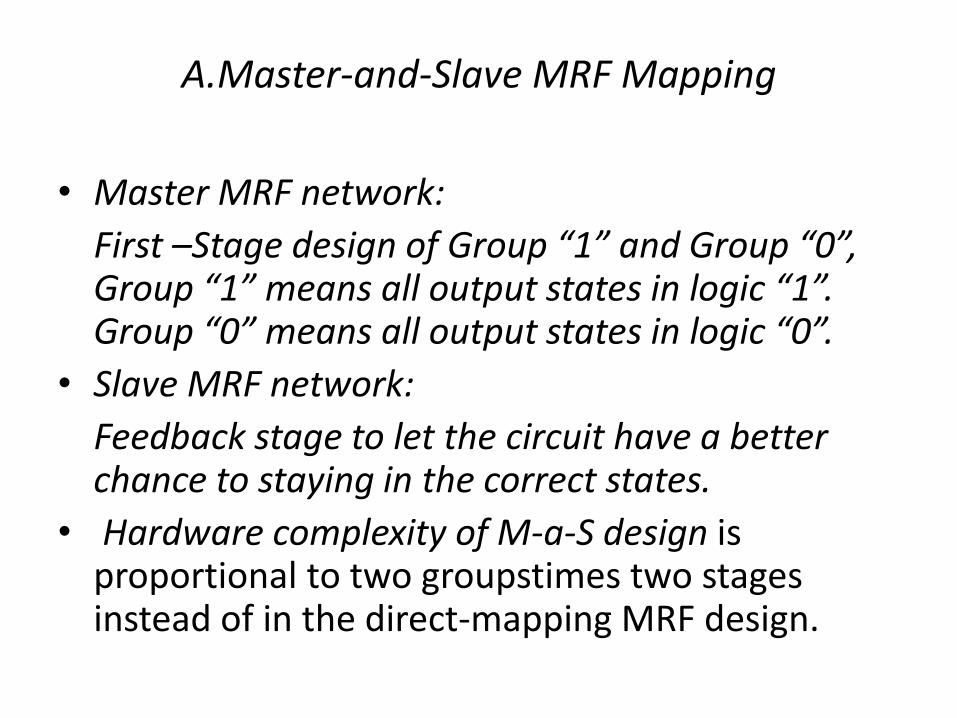
• Master MRF network:
First –Stage design of Group “1” and Group “0”, Group “1” means all output states in logic “1”. Group “0” means all output states in logic “0”.
• Slave MRF network:
Feedback stage to let the circuit have a better chance to staying in the correct states.
• Hardware complexity of M-a-S design is proportional to two groupstimes two stages instead of in the direct-mapping MRF design.
A.Master-and-Slave MRF Mapping

B. Master-and-Slave MRF Logic-Gate Construction
• In Fig7(b), the valid minterm generator is separated in two groups to fix the minterm number to two. In this way, we can prevent the exponential increase of hardware complexity in the valid minterm generator

• When summing all valid minterms, the compatibility function of a two-input NAND gate can be obtained by:
(1)
• By applying Boolean difference, (1) can be re-expressed as:
B. Master-and-Slave MRF Logic-Gate Construction

B. Master-and-Slave MRF Logic-Gate Construction
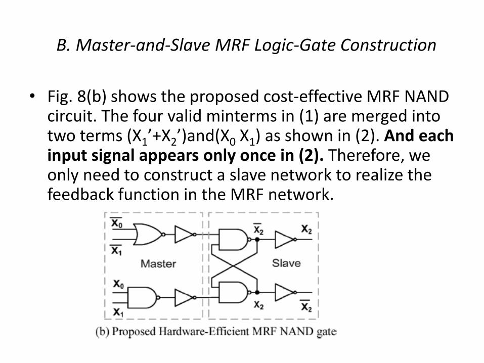
• Fig. 8(b) shows the proposed cost-effective MRF NAND circuit. The four valid minterms in (1) are merged into two terms (X1’+X2’)and(X0 X1) as shown in (2). And each input signal appears only once in (2). Therefore, we only need to construct a slave network to realize the feedback function in the MRF network.
B. Master-and-Slave MRF Logic-Gate Construction

• To illustrate the effect on area saving by adopting theproposed cost-effective master-and-slave MRF circuit, the transistor counts in the multiple-input NAND gates and Hamming decoders using the direct-mapping MRF approach in [1], the state-of-art cost-effective MRF design in [31], and the proposed master-and-slave MRF approach are compared. The comparison results are listed in Table I.
C. Comparison of Hardware Cost

• In the previous section, the mapping of simple logic gates onto MRF networks was discussed, This design is good for constructing basic MRF logic functions but is not suitable for constructing a complex and irregular Boolean function. In Section IV, we present a practical case of mapping an MRF network onto a computing system in order to meet the requirements of both performance and hardware cost.
IV. Practical MRF Noise-Tolerant Architecture Design

A. Local Network Mapping of MRF Noise-Tolerant Circuit
• We remap the M3 circuit in Fig. 1(a) onto a practical MRF network, as shown in Fig. 9.
• Global mapping means that the whole logic function is directly mapped onto the MRF network.
• Local mapping means that the whole logic circuit is divided into many submodules, which are then mapped onto MRF networks individually.
• The circuit complexity to implement the MRF network is determined by the number of nodes (or the possible valid states) N, in an MRF network defined as . If an MRF network is implemented by global mapping, all possible valid states in the MRF network are 2N-1, which means 2N-1 feedback loops must be constructed in order to construct the MRF network.
• Because the valid minterm feedback loop includes the feedforward and feedback parts, the hardware overhead in each feedback loop path is twice as large as the original CMOS design. As a result, the circuit complexity to implement the MRF network is 2N
A. Local Network Mapping of MRF Noise-Tolerant Circuit

A. Local Network Mapping of MRF Noise-Tolerant Circuit

• As shown in Fig. 10(b),N=7, 27=256 feedback loops must be constructed to implement a one-bit MRF full adder using the global mapping, while only 5 × 22=20 feedback loops need to be constructed to implement a one-bit MRF full adder using the local mapping in Fig. 10(c).
• Therefore, the local mapping technique is a more practical architectural mapping solution than the global mapping design to implement an MRF noise-tolerant computing system.
A. Local Network Mapping of MRF Noise-Tolerant Circuit

B. Analysis of the Noise-Tolerant Performance and Hardware Complexity of an MRF Network
• As an illustration, the global MRF network mapping method can achieve a superior noise-tolerance performance with a lower BER (bit-error rate )since all possible valid states are constructed and converged into a stable state. SNR(signal-to-noise ratio)

• The local network mapping technique, on the other hand, cannot achieve the same noise-tolerant ability as the global network mapping because some possible internal valid states in the MRF network are removed.
• However, the degradation of the noise-tolerant ability in local network mapping is very small and moreover, the design complexity and the critical path in the computing systems can be greatly reduced
• As a result, implementing the MRF noise-tolerant circuit with the local network mapping approach can provide a good tradeoff between noise-tolerant performance and design complexity and, thus, is a practical solution to implementing the MRF algorithm.
B. Analysis of the Noise-Tolerant Performance and Hardware Complexity of an MRF Network

C. Architectural Mapping of an 8-bit MRF_CLA Circuit

C. Architectural Mapping of an 8-bit MRF_CLA Circuit

C. Architectural Mapping of an 8-bit MRF_CLA Circuit

• The architecture of the proposed 8-bit MRF_CLA is shown in Fig. 15. In the MRF_CLA, the MRF subnetwork is constructed within only basic logical modules, such as MRF_INV, MRF_NAND/MRF_AND, MRF_NOR/MRF _OR, and MRF_XNOR/MRF_XOR circuits. Then, the whole 8-bit MRF_CLA circuit is hierarchically constructed using these MRF submicromodules.
C. Architectural Mapping of an 8-bit MRF_CLA Circuit

V. Chip Implementation And Measurement Results • A. Chip Implementation
• To demonstrate the proof-of-concept design, a master-andslave MRF chip, i.e., an 8-bit MRF_CLA, was fabricated using the TSMC 0.13- um CMOS process technology.
• The conventional and MRF CLA designs have also been implemented using the 0.18- um CMOS technology process to demonstrate and compare their performance in terms of noise tolerance, power, speed, and area [1].

B. Measurement Results
• 1) Measurement Setup to Test the MRF Circuit • The noise signals generated from the power supply are
AWGN. A power splitter is used to combine the noise-free input signal with AWGN. The measurement setup is shown in Fig. 17.

• 2) Measurement of the MRF Circuit Single-Bit Waveforms Under Noise Interference
B. Measurement Results

• 3) Measure Reduplicating Signals of the MRF Circuit Under Noise Interference
B. Measurement Results

• 4) Measurement of BER Under Various SNR in the MRF Circuit
B. Measurement Results

C. Chip Performance Summary

VI Conclusion
• In this paper, we have presented the design and implementation of a cost-effective probabilistically based noise-tolerant circuit, an 8-bit MRF_CLA, using the TSMC 0.13- um CMOS process. The proposed master-and-slave MRF_CLA can provide a 7.00*10-5BER under a 10.6-dB SNR, while the conventional CMOS_CLA can only provide an 8.84*10-3BER.
• The master-and-slave MRF_CLA can operate under 0.25 V to tolerate noise interference with only 1.9 uW/MHz of energy consumption. Moreover, the transistor count can be reduced by 42% as compared to the direct-mapping MRF_CLAdesign