cs 2204 spring 2007 experiment 4 lab 8. experiment 4 lab 8cs 2204 spring 2007 page 2 experiment 4...
Post on 22-Dec-2015
216 views
TRANSCRIPT
CS 2204 Spring 2007CS 2204 Spring 2007Experiment 4Lab 8
Experiment 4 Lab 8
CS 2204 Spring 2007
Page 2
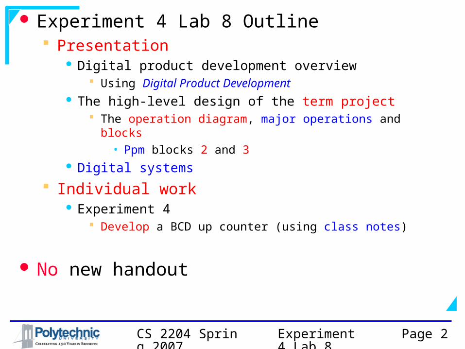
Experiment 4 Lab 8 Outline Presentation
Digital product development overview Using Digital Product Development
The high-level design of the term project The operation diagram, major operations and blocks
• Ppm blocks 2 and 3 Digital systems
Individual work Experiment 4
Develop a BCD up counter (using class notes)
No new handout
Experiment 4 Lab 8
CS 2204 Spring 2007
Page 3
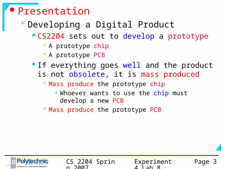
Presentation Developing a Digital Product
CS2204 sets out to develop a prototype A prototype chip A prototype PCB
If everything goes well and the product is not obsolete, it is mass produced
Mass produce the prototype chip• Whoever wants to use the chip must develop a
new PCB Mass produce the prototype PCB
Experiment 4 Lab 8
CS 2204 Spring 2007
Page 4
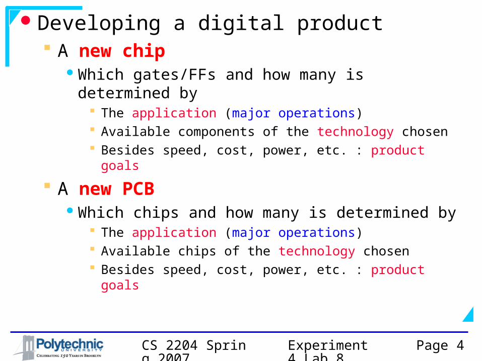
Developing a digital product A new chip
Which gates/FFs and how many is determined by
The application (major operations) Available components of the technology chosen Besides speed, cost, power, etc. : product goals
A new PCBWhich chips and how many is determined by
The application (major operations) Available chips of the technology chosen Besides speed, cost, power, etc. : product goals
Experiment 4 Lab 8
CS 2204 Spring 2007
Page 5
Developing a new chip
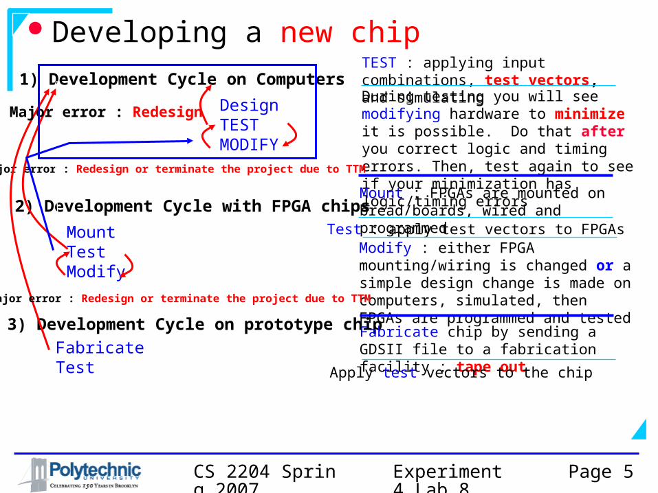
1) Development Cycle on Computers
DesignTESTMODIFY
During testing you will see modifying hardware to minimize it is possible. Do that after you correct logic and timing errors. Then, test again to see if your minimization has logic/timing errors
2) Development Cycle with FPGA chips
MountTestModify
Major error : Redesign or terminate the project due to TTM
Mount : FPGAs are mounted on bread/boards, wired and programmed
TEST : applying input combinations, test vectors, and simulating
Modify : either FPGA mounting/wiring is changed or a simple design change is made on computers, simulated, then FPGAs are programmed and tested
Test : apply test vectors to FPGAs
3) Development Cycle on prototype chip
FabricateTest
Fabricate chip by sending a GDSII file to a fabrication facility : tape outApply test vectors to the chip
Major error : Redesign or terminate the project due to TTM
Major error : Redesign
Experiment 4 Lab 8
CS 2204 Spring 2007
Page 6
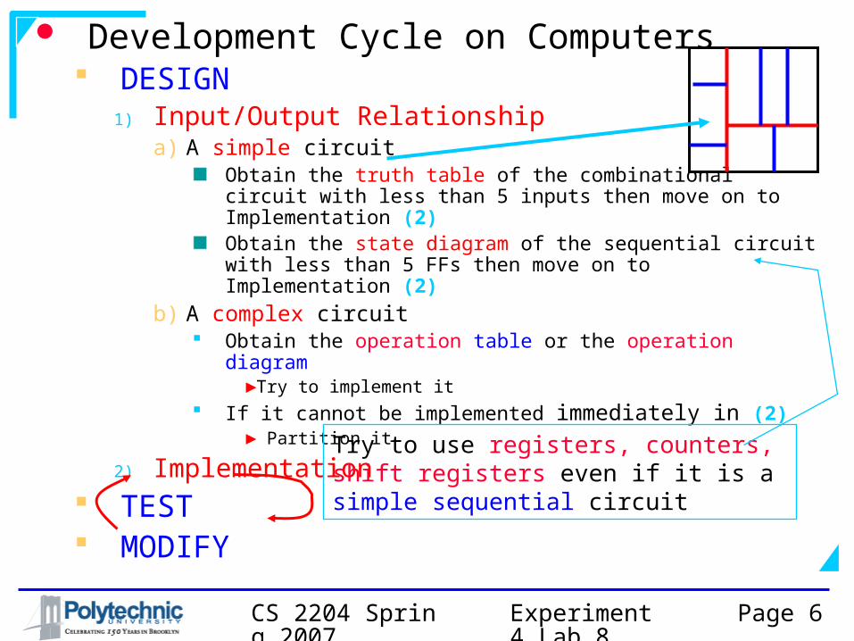
Development Cycle on Computers DESIGN
1) Input/Output Relationshipa) A simple circuit
Obtain the truth table of the combinational circuit with less than 5 inputs then move on to Implementation (2) Obtain the state diagram of the sequential circuit with less than 5 FFs then move on to Implementation (2)
b) A complex circuit Obtain the operation table or the operation diagram
►Try to implement it If it cannot be implemented immediately in (2)
► Partition it
2) Implementation TEST MODIFY
Try to use registers, counters, shift registers even if it is a simple sequential circuit
Experiment 4 Lab 8
CS 2204 Spring 2007
Page 7
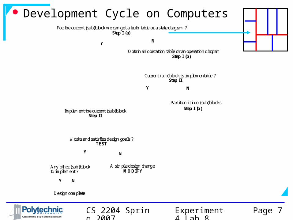
Development Cycle on ComputersFor the current (sub)block we can get a truth table or a state diagram ?
Current (sub)block is implementable ? Step II
Y
Obtain an operation table or an operation diagram Step I (b)
N
Any other (sub)blockto implement ?
Y
N
Design complete
Step I (a)
Works and satisfies design goals ? TEST
A simple design change MODIFY
Y
N
Implement the current (sub)block Step II
Y
Partition it into (sub)blocks Step I (b)
N
Experiment 4 Lab 8
CS 2204 Spring 2007
Page 8
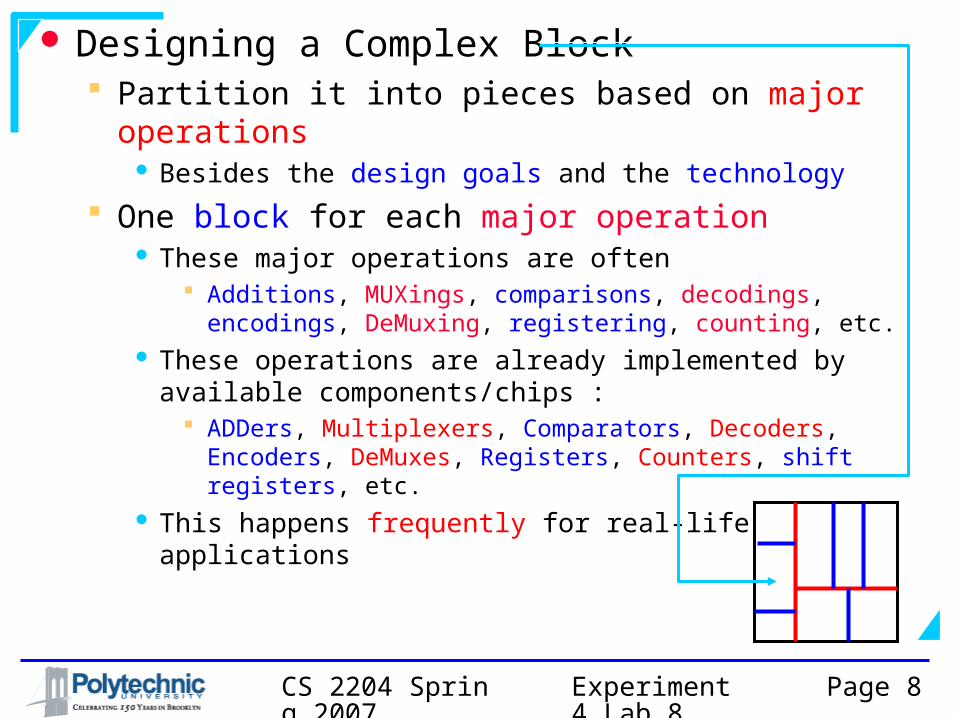
Designing a Complex Block Partition it into pieces based on major operations
Besides the design goals and the technology
One block for each major operation These major operations are often
Additions, MUXings, comparisons, decodings, encodings, DeMuxing, registering, counting, etc.
These operations are already implemented by available components/chips :
ADDers, Multiplexers, Comparators, Decoders, Encoders, DeMuxes, Registers, Counters, shift registers, etc.
This happens frequently for real-life applications

Experiment 4 Lab 8
CS 2204 Spring 2007
Page 9
An Unusual Major Operation (an unusual block) Trying to implement a block
If it has < 11 inputs implement it by using programmable components
Memory components• ROMs, RAMs
Otherwise (complex or too many inputs) Break it up or Repartition one level up, or
• Two levels up, or,…• All the way up (redesign !?)
Eventually, the resulting operations will be additions, comparisons, multiplexing, decoding, etc.
Experiment 4 Lab 8
CS 2204 Spring 2007
Page 10
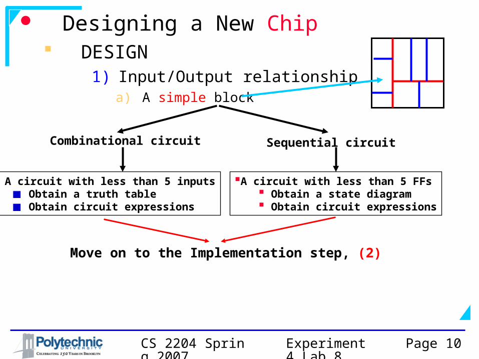
Designing a New Chip DESIGN
1) Input/Output relationshipa) A simple block
Move on to the Implementation step, (2)
Combinational circuit Sequential circuit
A circuit with less than 5 inputsObtain a truth tableObtain circuit expressions
A circuit with less than 5 FFs Obtain a state diagram Obtain circuit expressions
Experiment 4 Lab 8
CS 2204 Spring 2007
Page 11
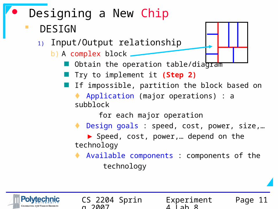
Designing a New Chip DESIGN
1) Input/Output relationshipb) A complex block
Obtain the operation table/diagramTry to implement it (Step 2)If impossible, partition the block based on Application (major operations) : a subblock
for each major operation Design goals : speed, cost, power, size,… ► Speed, cost, power,… depend on the technology Available components : components of the
technology
Experiment 4 Lab 8
CS 2204 Spring 2007
Page 12
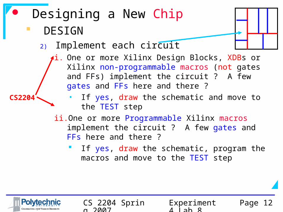
Designing a New Chip DESIGN
2) Implement each circuiti. One or more Xilinx Design Blocks, XDBs or Xilinx
non-programmable macros (not gates and FFs) implement the circuit ? A few gates and FFs here and there ?• If yes, draw the schematic and move to the
TEST stepii. One or more Programmable Xilinx macros
implement the circuit ? A few gates and FFs here and there ? If yes, draw the schematic, program the macros
and move to the TEST step
CS2204
Experiment 4 Lab 8
CS 2204 Spring 2007
Page 13
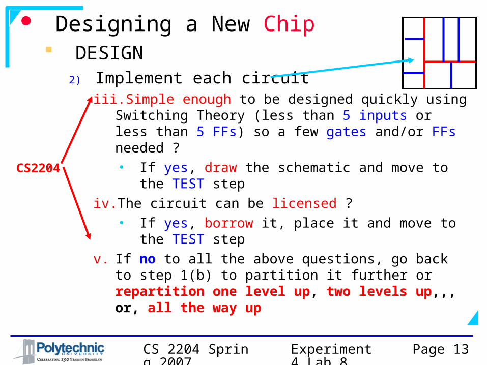
Designing a New Chip DESIGN
2) Implement each circuitiii. Simple enough to be designed quickly using
Switching Theory (less than 5 inputs or less than 5 FFs) so a few gates and/or FFs needed ?• If yes, draw the schematic and move to the
TEST stepiv. The circuit can be licensed ?
• If yes, borrow it, place it and move to the TEST step
v. If no to all the above questions, go back to step 1(b) to partition it further or repartition one level up, two levels up,,, or, all the way up
CS2204
Experiment 4 Lab 8
CS 2204 Spring 2007
Page 14
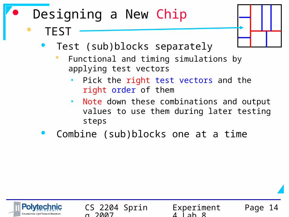
Designing a New Chip TEST
Test (sub)blocks separately Functional and timing simulations by applying test
vectors• Pick the right test vectors and the right order of
them• Note down these combinations and output
values to use them during later testing steps Combine (sub)blocks one at a time
Experiment 4 Lab 8
CS 2204 Spring 2007
Page 15
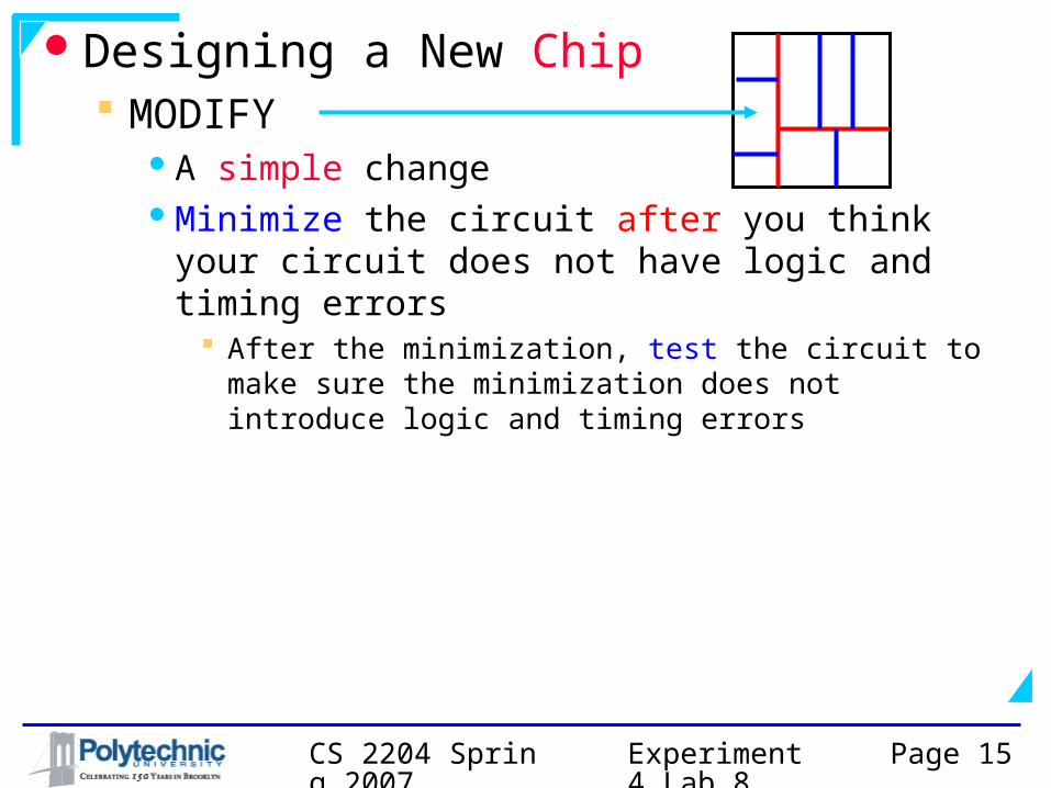
Designing a New Chip MODIFY
A simple changeMinimize the circuit after you think your circuit
does not have logic and timing errors After the minimization, test the circuit to make sure
the minimization does not introduce logic and timing errors
Experiment 4 Lab 8
CS 2204 Spring 2007
Page 16
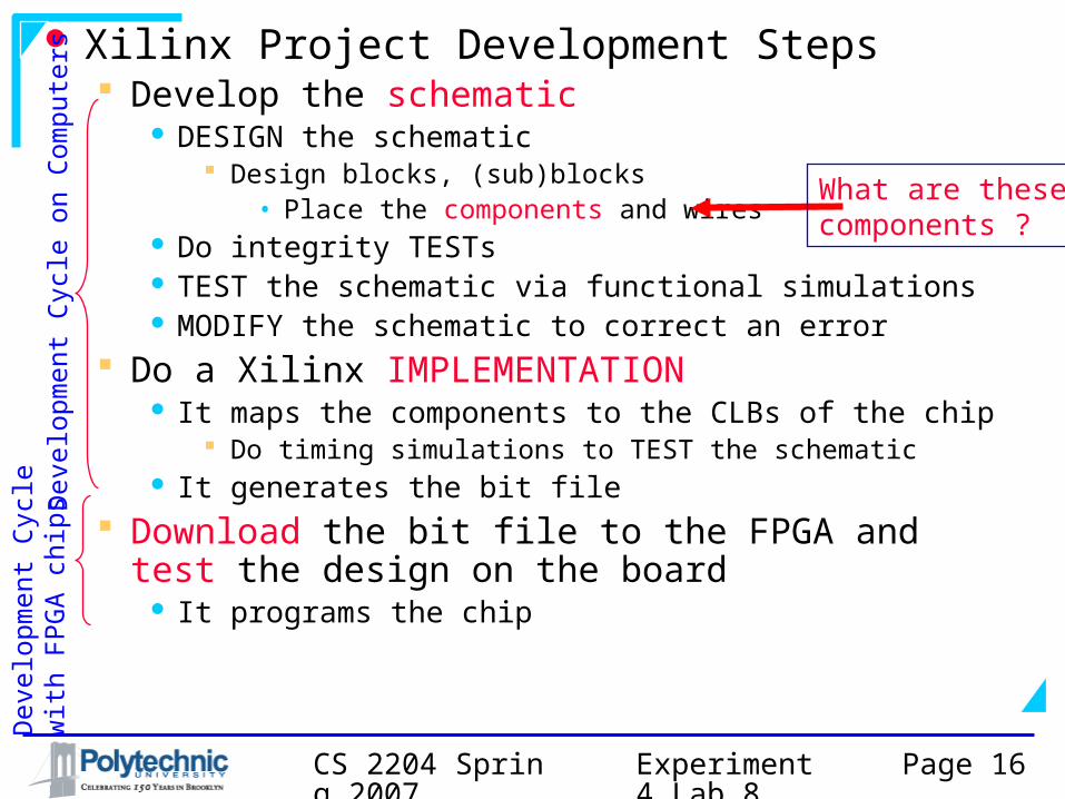
Xilinx Project Development Steps Develop the schematic
DESIGN the schematic Design blocks, (sub)blocks
• Place the components and wires Do integrity TESTs TEST the schematic via functional simulations MODIFY the schematic to correct an error
Do a Xilinx IMPLEMENTATION It maps the components to the CLBs of the chip
Do timing simulations to TEST the schematic It generates the bit file
Download the bit file to the FPGA and test the design on the board
It programs the chip
What are thesecomponents ?
Dev
elop
men
t Cyc
le o
n C
ompu
ters
Dev
elop
men
t Cyc
lew
ith
FPG
A c
hips
Experiment 4 Lab 8
CS 2204 Spring 2007
Page 17
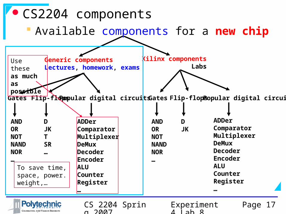
CS2204 components Available components for a new chip
Generic componentsLectures, homework, exams
Xilinx components Labs
Gates Flip-flopsPopular digital circuits Gates Flip-flops Popular digital circuits
ANDORNOTNANDNOR…
DJKTSR…
ADDerComparatorMultiplexerDeMuxDecoderEncoderALUCounterRegister…
ANDORNOTNANDNOR…
DJK
ADDerComparatorMultiplexerDeMuxDecoderEncoderALUCounterRegister…
Use these as much as possible
To save time,space, power.weight,…
Experiment 4 Lab 8
CS 2204 Spring 2007
Page 18
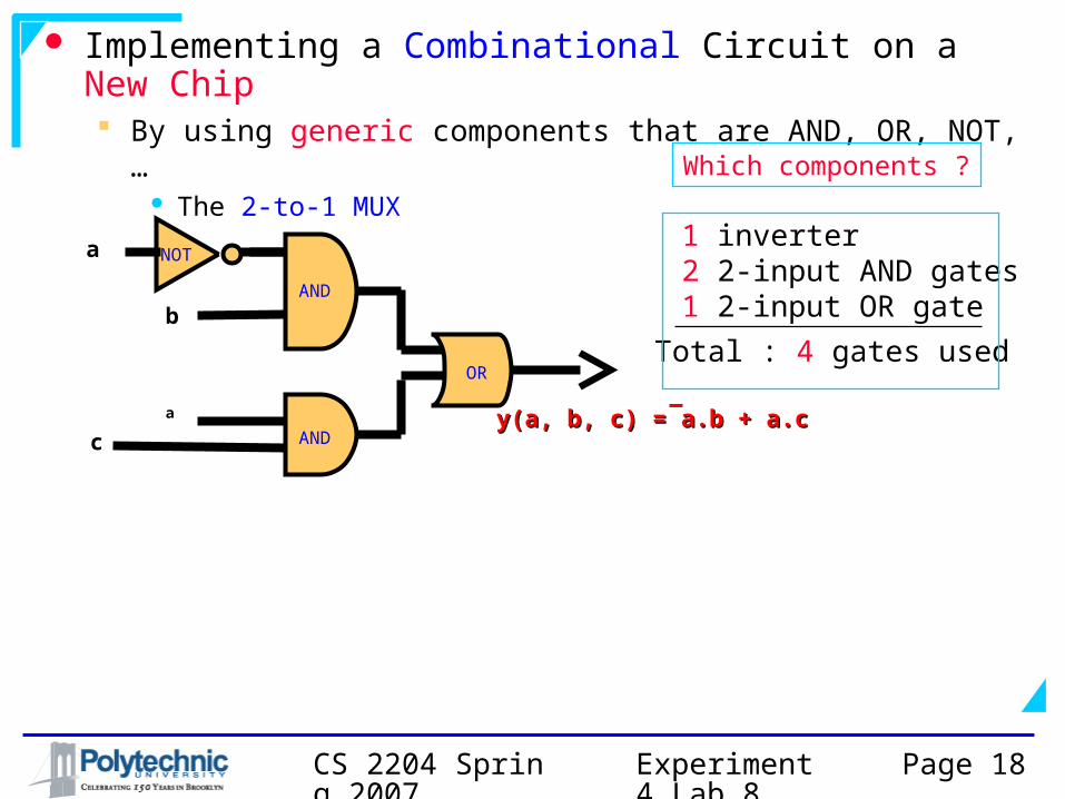
Implementing a Combinational Circuit on a New Chip By using generic components that are AND, OR, NOT,…
The 2-to-1 MUX
AND
AND
OR
NOTa
b
a
cy(a, b, c) =y(a, b, c) = a.b + a.ca.b + a.c
1 inverter2 2-input AND gates1 2-input OR gate
Total : 4 gates used
Which components ?
Experiment 4 Lab 8
CS 2204 Spring 2007
Page 19
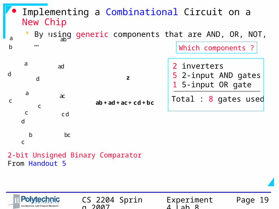
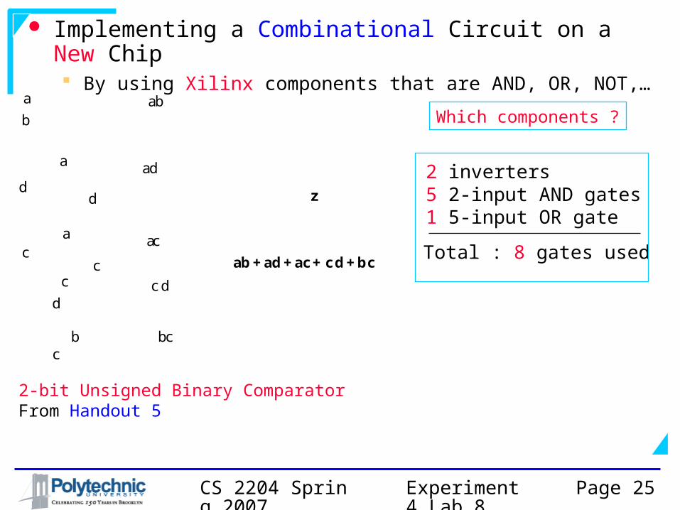
Implementing a Combinational Circuit on a New Chip By using generic components that are AND, OR, NOT,…a
b
d
a
ca
c
d
z
bc
d
c
ab
ad
ac
c d
bc
2-bit Unsigned Binary ComparatorFrom Handout 5
ab + ad + ac + c d + bc Total : 8 gates used
2 inverters5 2-input AND gates1 5-input OR gate
Which components ?
Experiment 4 Lab 8
CS 2204 Spring 2007
Page 20
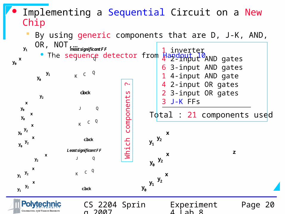
Implementing a Sequential Circuit on a New Chip By using generic components that are D, J-K, AND, OR,
NOT,… The sequence detector from Handout 10
J
K C
Q
Q
y2
y1
xy0
y1y
0
clock
most significant FF
J
K C
Q
Q
xy2
y2y1
y2y1clock
x
x
y0
Least significant FF
J
K C
Q
Q
y2
xy0
xy
0
xy
2y0x
y2y
0
clock
y1
y2y1
y2y0
y2y1
y0
z
x
x
x
Total : 21 components used
1 inverter4 2-input AND gates6 3-input AND gates1 4-input AND gate4 2-input OR gates2 3-input OR gates3 J-K FFs
Whic
h c
om
ponents
?

Experiment 4 Lab 8
CS 2204 Spring 2007
Page 21
CS2204 Components Available components for a new chip
Generic componentsLectures, homework, exams
Xilinx componentsLabs
Gates Flip-flops Popular digital circuits Gates Flip-flops Popular digital circuits
ANDORNOTNANDNOR…
DJKTSR
ADDerComparatorMultiplexerDeMuxDecoderEncoderALUCounterRegister…
ANDORNOTNANDNOR…
DTJK
ADDerComparatorMultiplexerDeMuxDecoderEncoderALUCounterRegister…
Lab design
Use Xilinx macros as much as possible
Try not to use these components
Experiment 4 Lab 8
CS 2204 Spring 2007
Page 22
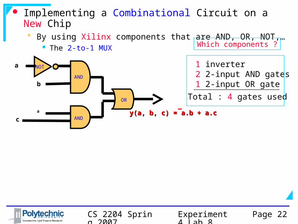
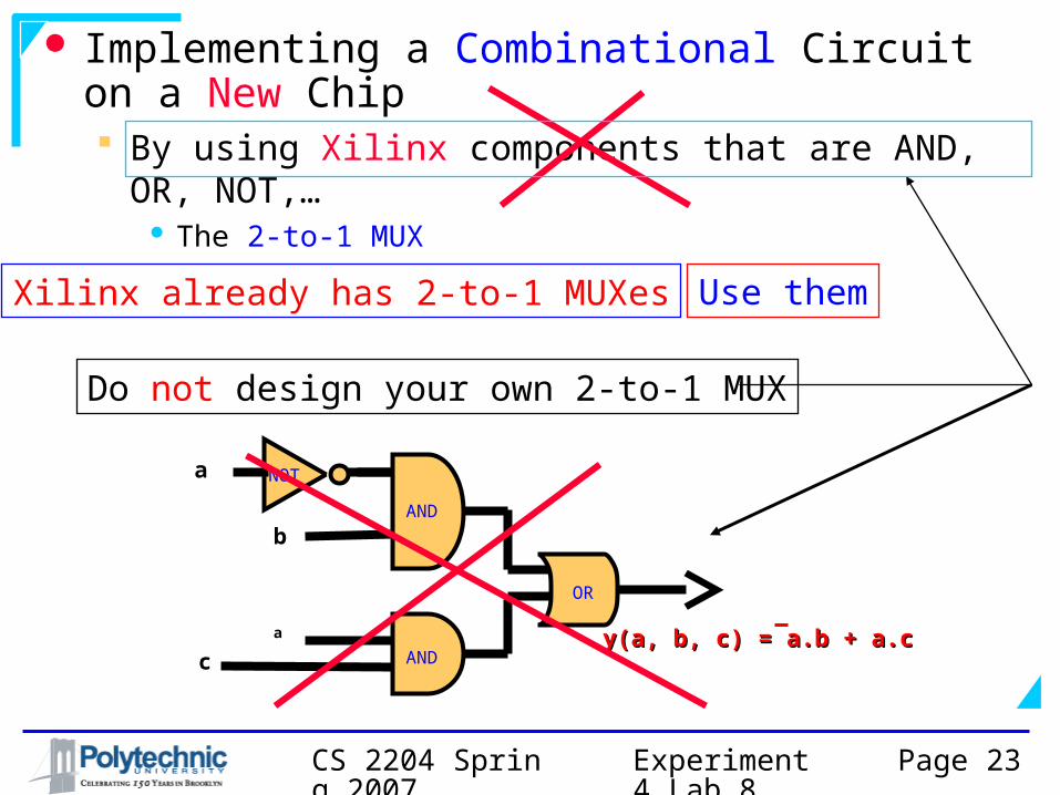
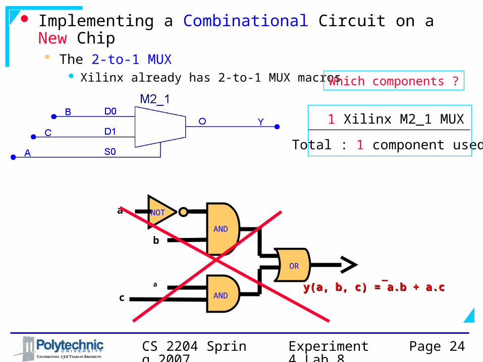
Implementing a Combinational Circuit on a New Chip By using Xilinx components that are AND, OR, NOT,…
The 2-to-1 MUX
AND
AND
OR
NOTa
b
a
cy(a, b, c) =y(a, b, c) = a.b + a.ca.b + a.c
1 inverter2 2-input AND gates1 2-input OR gate
Total : 4 gates used
Which components ?
Experiment 4 Lab 8
CS 2204 Spring 2007
Page 23
Implementing a Combinational Circuit on a New Chip By using Xilinx components that are AND, OR,
NOT,… The 2-to-1 MUX
Xilinx already has 2-to-1 MUXes Use them
AND
AND
OR
NOTa
b
a
cy(a, b, c) =y(a, b, c) = a.b + a.ca.b + a.c
Do not design your own 2-to-1 MUX
Experiment 4 Lab 8
CS 2204 Spring 2007
Page 24
Implementing a Combinational Circuit on a New Chip The 2-to-1 MUX
Xilinx already has 2-to-1 MUX macros M2_1
AND
AND
OR
NOTa
b
a
cy(a, b, c) =y(a, b, c) = a.b + a.ca.b + a.c
1 Xilinx M2_1 MUX
Total : 1 component used
Which components ?
Experiment 4 Lab 8
CS 2204 Spring 2007
Page 25
Implementing a Combinational Circuit on a New Chip By using Xilinx components that are AND, OR, NOT,…
a
b
d
a
ca
c
d
z
bc
d
c
ab
ad
ac
c d
bc
ab + ad + ac + c d + bc Total : 8 gates used
2 inverters5 2-input AND gates1 5-input OR gate
2-bit Unsigned Binary ComparatorFrom Handout 5
Which components ?
Experiment 4 Lab 8
CS 2204 Spring 2007
Page 26
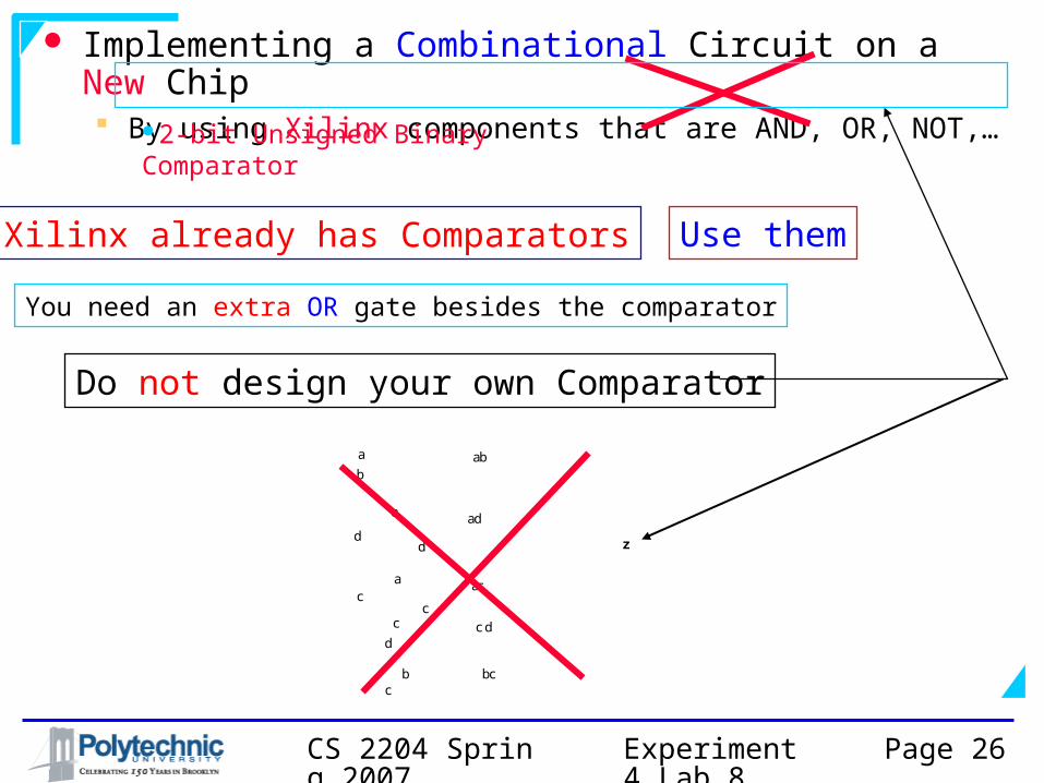
Implementing a Combinational Circuit on a New Chip By using Xilinx components that are AND, OR, NOT,…
Xilinx already has Comparators Use them
You need an extra OR gate besides the comparator
2-bit Unsigned Binary Comparator
a
b
d
a
ca
c
d
z
bc
d
c
ab
ad
ac
c d
bc
Do not design your own Comparator
Experiment 4 Lab 8
CS 2204 Spring 2007
Page 27
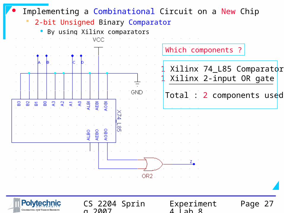
Implementing a Combinational Circuit on a New Chip 2-bit Unsigned Binary Comparator
By using Xilinx comparators
1 Xilinx 74_L85 Comparator1 Xilinx 2-input OR gate
Total : 2 components used
Which components ?
Experiment 4 Lab 8
CS 2204 Spring 2007
Page 28
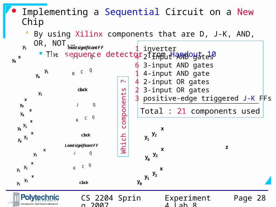
Implementing a Sequential Circuit on a New Chip By using Xilinx components that are D, J-K, AND, OR, NOT,
… The sequence detector from Handout 10
J
K C
Q
Q
y2
y1
xy0
y1y
0
clock
most significant FF
J
K C
Q
Q
xy2
y2y1
y2y1clock
x
x
y0
Least significant FF
J
K C
Q
Q
y2
xy0
xy
0
xy
2y0x
y2y
0
clock
y1
y2y1
y2y0
y2y1
y0
z
x
x
x
Total : 21 components used
1 inverter4 2-input AND gates6 3-input AND gates1 4-input AND gate4 2-input OR gates2 3-input OR gates3 positive-edge triggered J-K FFs
Whic
h c
om
ponents
?
Experiment 4 Lab 8
CS 2204 Spring 2007
Page 29
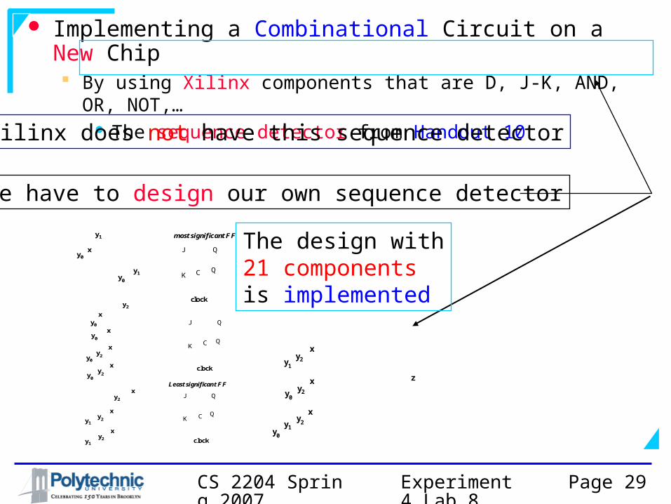
Implementing a Combinational Circuit on a New Chip By using Xilinx components that are D, J-K, AND, OR, NOT,
… The sequence detector from Handout 10Xilinx does not have this sequence detector
J
K C
Q
Q
y2
y1
xy0
y1y
0
clock
most significant FF
J
K C
Q
Q
xy2
y2y1
y2y1clock
x
x
y0
Least significant FF
J
K C
Q
Q
y2
xy0
xy
0
xy
2y0x
y2y
0
clock
y1
y2y1
y2y0
y2y1
y0
z
x
x
x
We have to design our own sequence detector
The design with21 components is implemented
Experiment 4 Lab 8
CS 2204 Spring 2007
Page 30
Xilinx FFs, Registers, Counters Many do not have direct set and direct
clear inputsTo avoid cases where both are active
They have either A direct set input
OrA direct clear input
Experiment 4 Lab 8
CS 2204 Spring 2007
Page 31
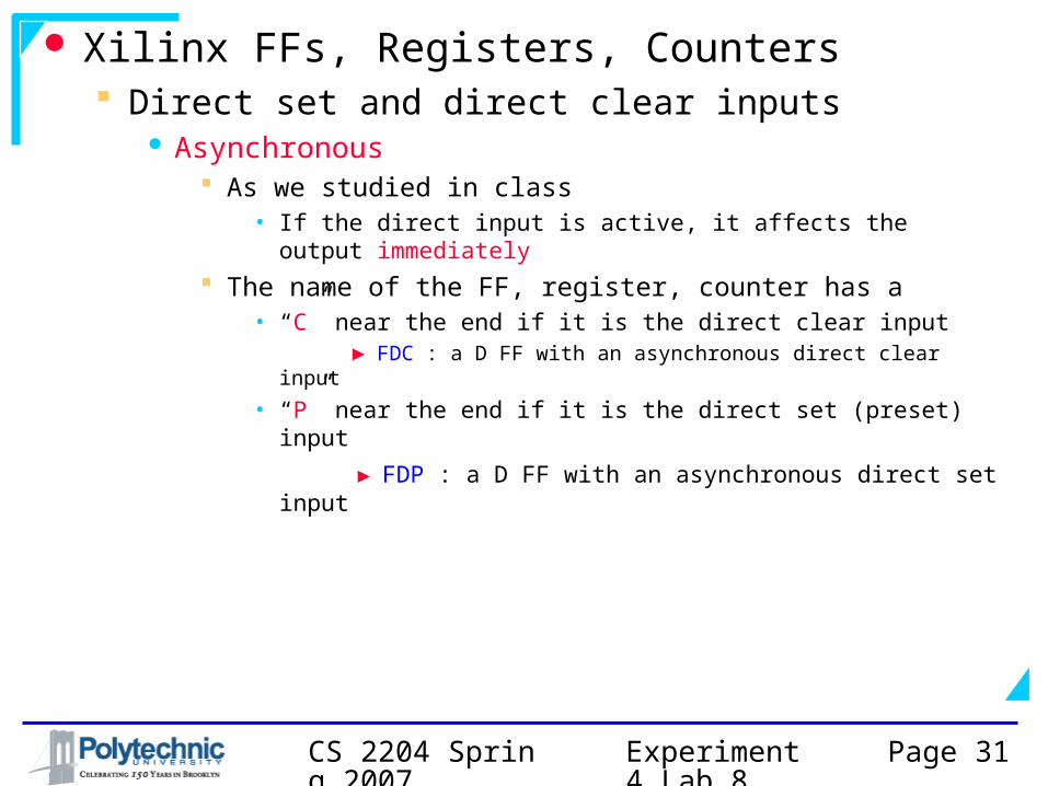
Xilinx FFs, Registers, Counters Direct set and direct clear inputs
Asynchronous As we studied in class
• If the direct input is active, it affects the output immediately The name of the FF, register, counter has a
• “C” near the end if it is the direct clear input ► FDC : a D FF with an asynchronous direct clear input
• “P” near the end if it is the direct set (preset) input
► FDP : a D FF with an asynchronous direct set input
Experiment 4 Lab 8
CS 2204 Spring 2007
Page 32
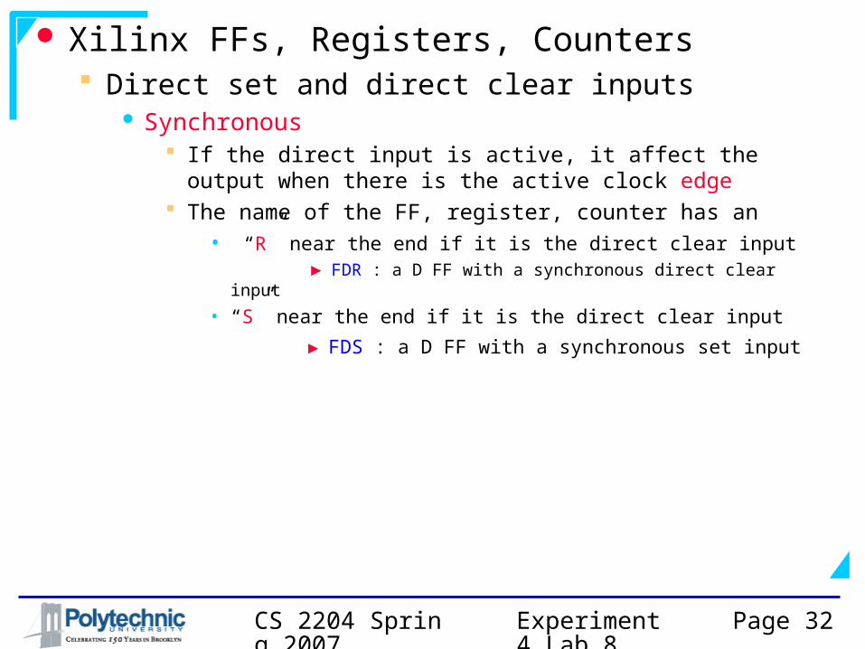
Xilinx FFs, Registers, Counters Direct set and direct clear inputs
Synchronous If the direct input is active, it affect the output when there
is the active clock edge The name of the FF, register, counter has an
• “R” near the end if it is the direct clear input ► FDR : a D FF with a synchronous direct clear input
• “S” near the end if it is the direct clear input
► FDS : a D FF with a synchronous set input
Experiment 4 Lab 8
CS 2204 Spring 2007
Page 33
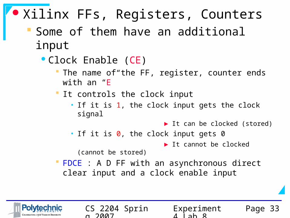
Xilinx FFs, Registers, Counters Some of them have an additional input
Clock Enable (CE) The name of the FF, register, counter ends with an
“E” It controls the clock input
• If it is 1, the clock input gets the clock signal► It can be clocked (stored)
• If it is 0, the clock input gets 0► It cannot be clocked (cannot be
stored)
FDCE : A D FF with an asynchronous direct clear input and a clock enable input
Experiment 4 Lab 8
CS 2204 Spring 2007
Page 34
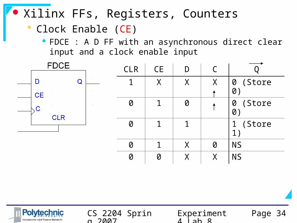
Xilinx FFs, Registers, Counters Clock Enable (CE)
FDCE : A D FF with an asynchronous direct clear input and a clock enable input
CLR CE D C Q1 X X X 0 (Store 0)0 1 0 0 (Store 0)
0 1 1 1 (Store 1)
0 1 X 0 NS0 0 X X NS
Experiment 4 Lab 8
CS 2204 Spring 2007
Page 35
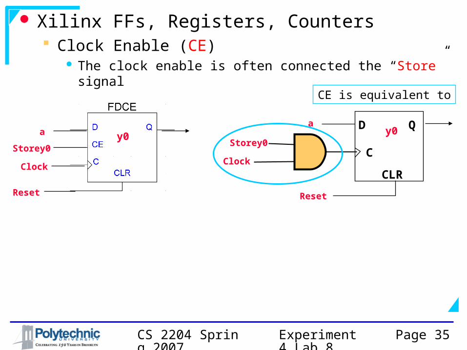
Xilinx FFs, Registers, Counters Clock Enable (CE)
The clock enable is often connected the “Store” signal
a
Storey0
Clock
Reset
y0D
C
CLR
Qa
Reset
y0
CE is equivalent to
Storey0
Clock
Experiment 4 Lab 8
CS 2204 Spring 2007
Page 36
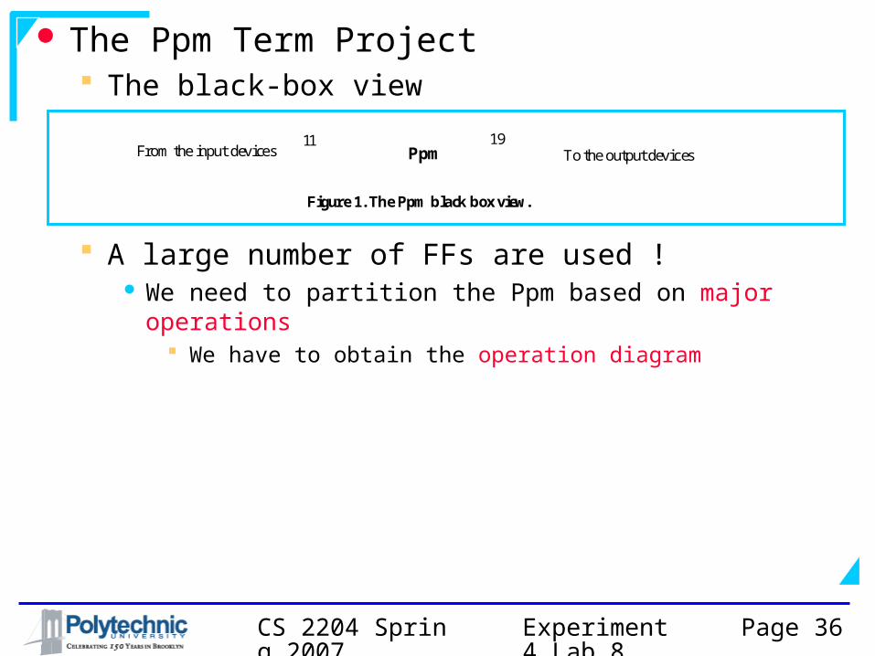
The Ppm Term Project The black-box view
A large number of FFs are used ! We need to partition the Ppm based on major operations
We have to obtain the operation diagram
Figure 1. The Ppm black box view.
Ppm11 19
From the input devices To the output devices
Experiment 4 Lab 8
CS 2204 Spring 2007
Page 37
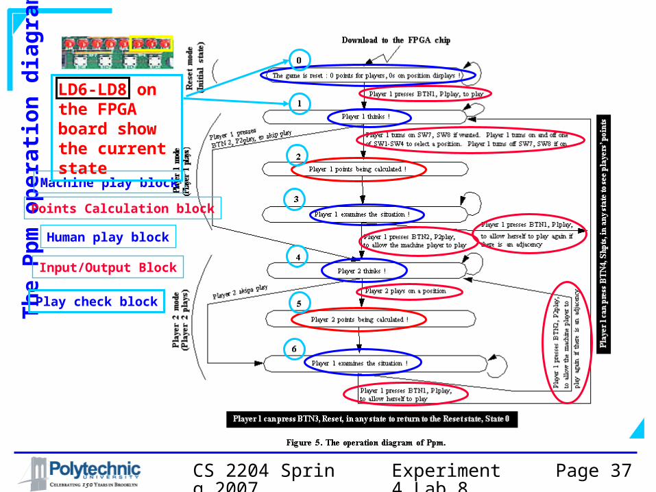
Th
e P
pm
op
erat
ion
dia
gram
Points Calculation block
Machine play block
Human play block
Input/Output Block
Play check block
LD6-LD8 on the FPGA board show the current state
Experiment 4 Lab 8
CS 2204 Spring 2007
Page 38
The Ppm Term Project Partitioning We have observed the following major operations
Interfacing to the input/output devices Handling human player’s play Controlling display operations based on game rules Calculating new player points Determining the machine player play
Hint for general partitioning If you cannot figure out major operations,
partition one major operation at a time
Experiment 4 Lab 8
CS 2204 Spring 2007
Page 39
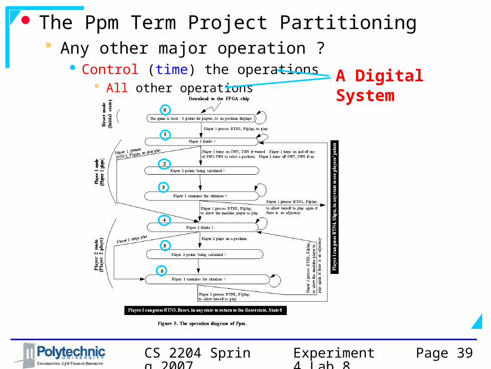
The Ppm Term Project Partitioning Any other major operation ?
Control (time) the operations All other operations
A Digital System
Experiment 4 Lab 8
CS 2204 Spring 2007
Page 40
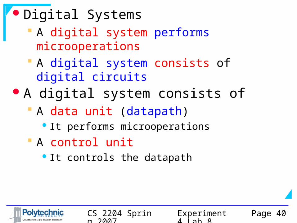
Digital Systems A digital system performs microoperations A digital system consists of digital circuits
A digital system consists of A data unit (datapath)
It performs microoperations
A control unit It controls the datapath
Experiment 4 Lab 8
CS 2204 Spring 2007
Page 41
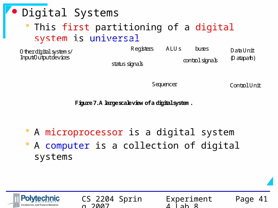
Digital Systems This first partitioning of a digital system is
universal
A microprocessor is a digital system A computer is a collection of digital systems
control signalsstatus signals
Sequencer
Registers ALUs buses Data Unit
Control Unit
Figure 7. A large scale view of a digital system.
Other digital systems/Input/Output devices (Datapath)
Experiment 4 Lab 8
CS 2204 Spring 2007
Page 42
Digital Systems The data unit has registers, ALUs and
buses to perform microoperationsRegisters keep (store) data (operands and
results)Arithmetic Logic Units (ALUs) perform
additions, subtractions, multiplications, ANDS, ORs, etc.
Buses interconnect registers and ALUs
Experiment 4 Lab 8
CS 2204 Spring 2007
Page 43
Digital Systems The data unit is highly regular
Pieces of hardware repeated many times 1-bit MUX repeated 32 times for a 32-bit MUX 4-bit ADDer repeated 8 times for a 32-bit ADDer
It is easier to design, test, modify, manufacture, upgrade, service, maintain regular hardware
Experiment 4 Lab 8
CS 2204 Spring 2007
Page 44
Digital Systems The control unit determines the sequence
of microoperations based on status signalsThe control unit goes through steps (states)
In each state, it enables the microoperations of that state to happen in the data unit based on the status signals
• Microoperations must start at the right time with correct inputs and end at the right time with correct outputs
• Glitches, gate delays must be accounted for
Experiment 4 Lab 8
CS 2204 Spring 2007
Page 45
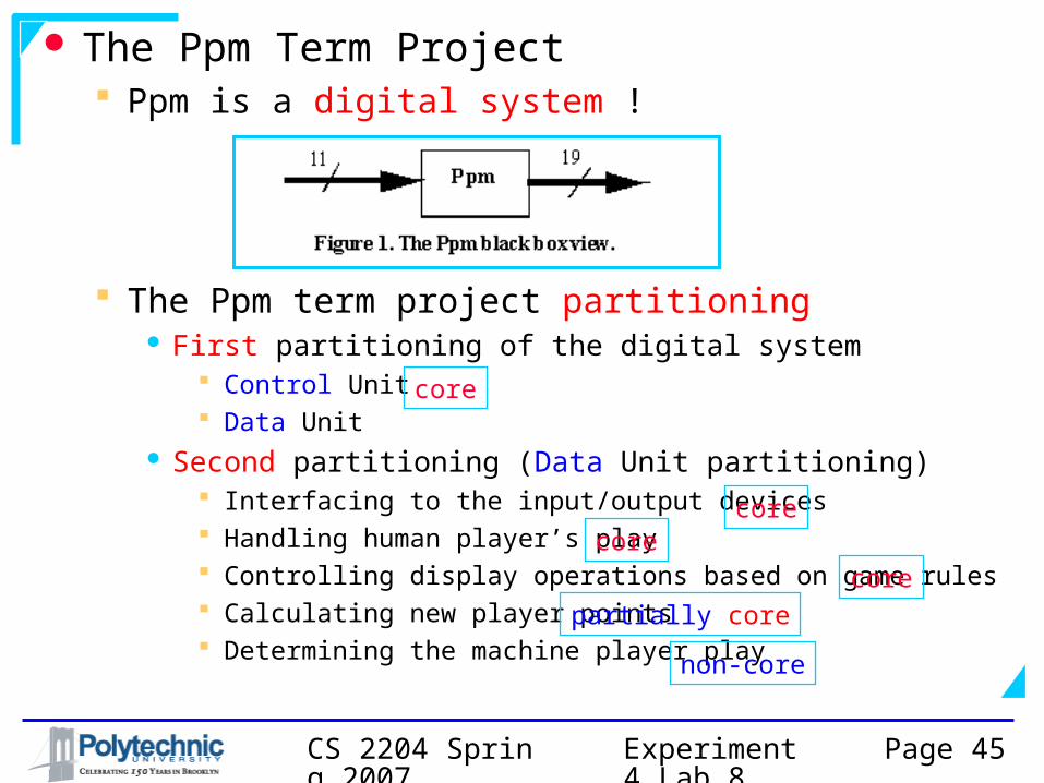
The Ppm Term Project Ppm is a digital system !
The Ppm term project partitioning First partitioning of the digital system
Control Unit Data Unit
Second partitioning (Data Unit partitioning) Interfacing to the input/output devices Handling human player’s play Controlling display operations based on game rules Calculating new player points Determining the machine player play
core
corecore
corepartially core
non-core
Experiment 4 Lab 8
CS 2204 Spring 2007
Page 46
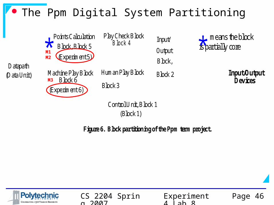
The Ppm Digital System Partitioning
Input/Output Devices
Control Unit, Block 1
Play Check Block
Figure 6. Block partitioning of the Ppm term project.
(Block 1)
Block 4
Machine Play BlockBlock 6
Datapath(Data Unit)
(Experiment 6)
Core
means the blockis partially core
Human Play Block
Block 3 Core
Points Calculation
Block, Block 5
(Experiment 5)
Input/
Block,
Block 2
Output
Core
**Core
M1M2
M3
Experiment 4 Lab 8
CS 2204 Spring 2007
Page 47
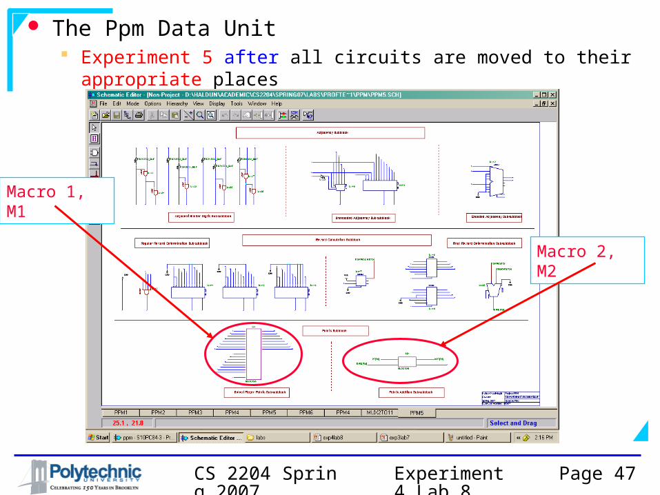
The Ppm Data Unit Experiment 5 after all circuits are moved to their
appropriate places
Macro 2, M2
Macro 1, M1
Experiment 4 Lab 8
CS 2204 Spring 2007
Page 48
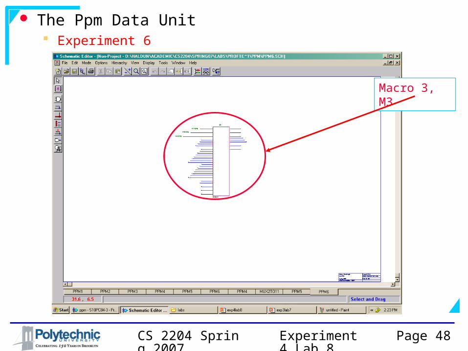
The Ppm Data Unit Experiment 6
Macro 3, M3
Experiment 4 Lab 8
CS 2204 Spring 2007
Page 49
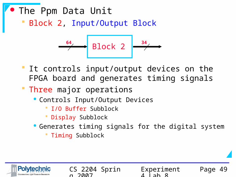
The Ppm Data Unit Block 2, Input/Output Block
It controls input/output devices on the FPGA board and generates timing signals
Three major operations Controls Input/Output Devices
I/O Buffer Subblock Display Subblock
Generates timing signals for the digital system Timing Subblock
Block 264 34
Experiment 4 Lab 8
CS 2204 Spring 2007
Page 50
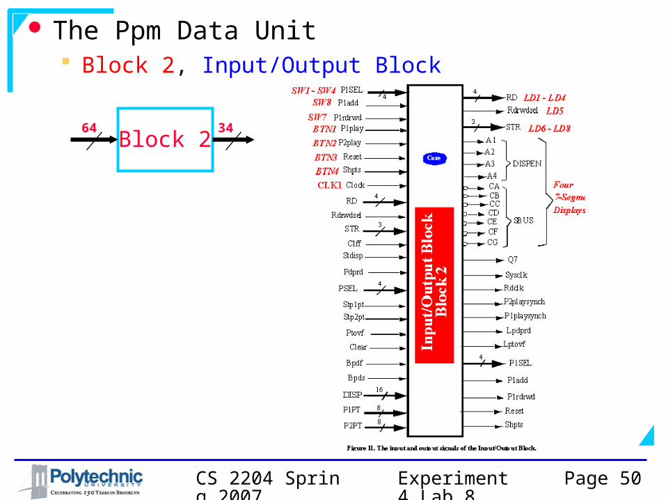
The Ppm Data Unit Block 2, Input/Output Block
Block 264 34

Experiment 4 Lab 8
CS 2204 Spring 2007
Page 51
The Ppm Data Unit Block 2, Input/Output Block
I/O BufferSubblock
TimingSubblock
DisplaySubblock
32-bit frequency divider
Experiment 4 Lab 8
CS 2204 Spring 2007
Page 52
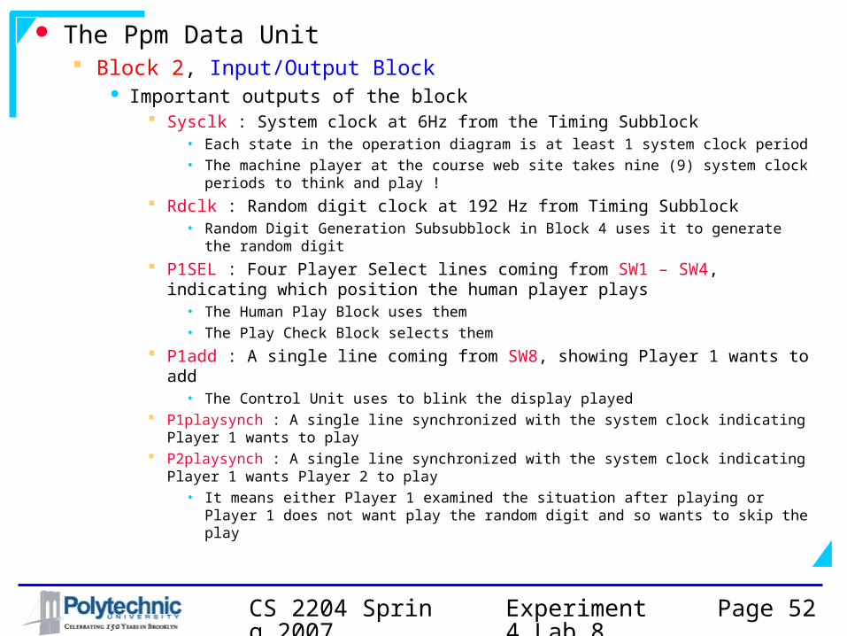
The Ppm Data Unit Block 2, Input/Output Block
Important outputs of the block Sysclk : System clock at 6Hz from the Timing Subblock
• Each state in the operation diagram is at least 1 system clock period• The machine player at the course web site takes nine (9) system clock
periods to think and play ! Rdclk : Random digit clock at 192 Hz from Timing Subblock
• Random Digit Generation Subsubblock in Block 4 uses it to generate the random digit
P1SEL : Four Player Select lines coming from SW1 – SW4, indicating which position the human player plays
• The Human Play Block uses them• The Play Check Block selects them
P1add : A single line coming from SW8, showing Player 1 wants to add
• The Control Unit uses to blink the display played P1playsynch : A single line synchronized with the system clock indicating
Player 1 wants to play P2playsynch : A single line synchronized with the system clock indicating
Player 1 wants Player 2 to play• It means either Player 1 examined the situation after playing or Player 1
does not want play the random digit and so wants to skip the play

Experiment 4 Lab 8
CS 2204 Spring 2007
Page 53
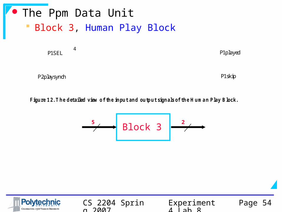
The Ppm Data Unit Block 3, Human Play Block
Very simple for this version of the term project Makes sure the human player does not play on two or
more positions Generates P1played and P1skip signals
It is kept there so that in the future this block can be used to have another machine player so that it becomes machine vs. machine
Block 35 2
Experiment 4 Lab 8
CS 2204 Spring 2007
Page 54
The Ppm Data Unit Block 3, Human Play Block
Block 35 2
P1SEL4
P1skip
P1played
Figure 12. The detailed view of the input and output signals of the Human Play Block.
Human Play Block
P2playsynchCore
Block 3
Experiment 4 Lab 8
CS 2204 Spring 2007
Page 55
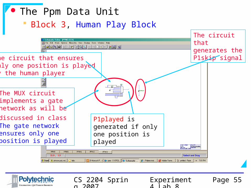
The Ppm Data Unit Block 3, Human Play Block
The circuit that ensuresonly one position is played by the human player
The MUX circuit implements a gate network as will be
discussed in class The gate networkensures only one position is played
The circuit that generates the P1skip signal
P1played is generated if only one position is played
Experiment 4 Lab 8
CS 2204 Spring 2007
Page 56
The Ppm Data Unit Block 3, Human Play Block
Important outputs of the block P1played : A single line indicating Player 1 has
played on a position• It is 1 if only one of SW1 – SW4 is turned on
► The MUX circuit ensures only one position is played
P1skip : A single line indicating Player 1 has skipped the play
• The P2play line is used to generate P1skip ► If Player 1 turns on P2play, it means Player 1 does not
want play the random digit ≡ Player 1 wants to skip
► A buffer is used to rename the P2playsynch signal
Experiment 4 Lab 8
CS 2204 Spring 2007
Page 57
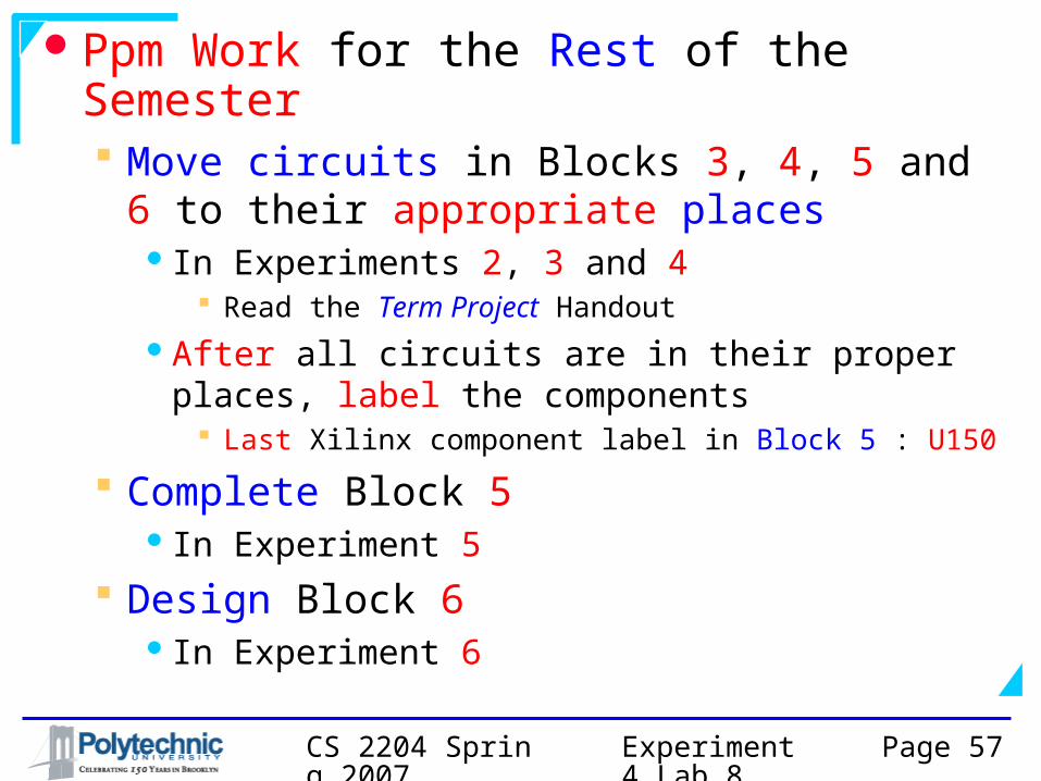
Ppm Work for the Rest of the Semester Move circuits in Blocks 3, 4, 5 and 6 to
their appropriate places In Experiments 2, 3 and 4
Read the Term Project HandoutAfter all circuits are in their proper places,
label the components Last Xilinx component label in Block 5 : U150
Complete Block 5 In Experiment 5
Design Block 6 In Experiment 6
Experiment 4 Lab 8
CS 2204 Spring 2007
Page 58
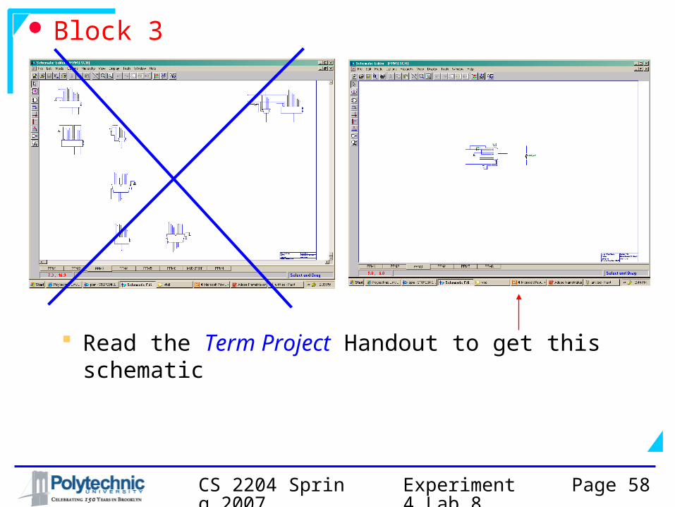
Block 3
Read the Term Project Handout to get this schematic
Experiment 4 Lab 8
CS 2204 Spring 2007
Page 59
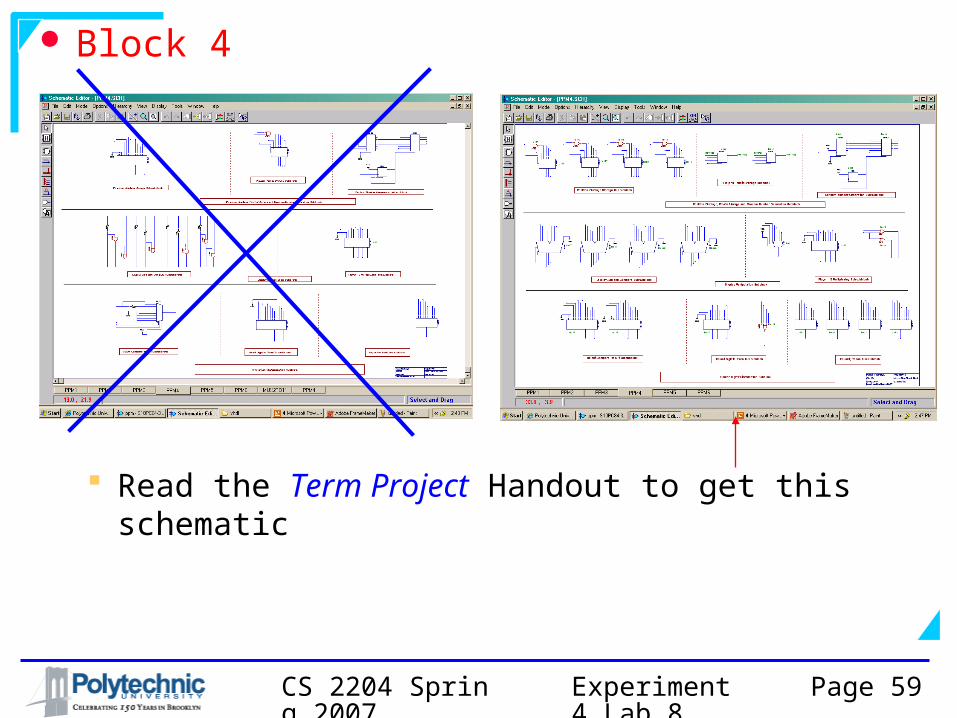
Block 4
Read the Term Project Handout to get this schematic
Experiment 4 Lab 8
CS 2204 Spring 2007
Page 60
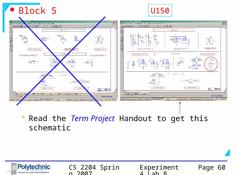
Block 5
Read the Term Project Handout to get this schematic
U150
Experiment 4 Lab 8
CS 2204 Spring 2007
Page 61
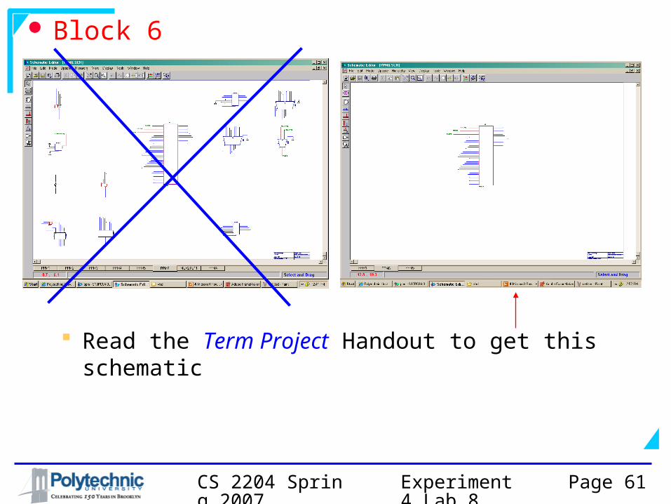
Block 6
Read the Term Project Handout to get this schematic
Experiment 4 Lab 8
CS 2204 Spring 2007
Page 62
Q/A
Do not leave the lab before your partners finish► Help your partners complete today’s project
Read slides on the Ppm, Project Manager, Schematic design and other related topics
Continue reading the Term Project handout
Think about the machine player strategy

Experiment 4 Lab 8
CS 2204 Spring 2007
Page 63
Today’s Individual Xilinx Work We will study (analyze) the term project
We will use our knowledge of counters to modify a portion of a term project schematic
We will replace a 4-bit Xilinx BCD up counter (Divide-by-10 or Modulo-10 counter) with our own circuits
Read slides on the Ppm, Project Manager, Schematic design and other related topics
Help your partners complete today’s project Continue reading the Term Project handout
Move circuits in Blocks 3, 4, 5 and 6 to their appropriate places
In Experiments 2, 3 and 4 After all circuits are in their proper places, label the
components Last Xilinx component label in Block 5 : U150
Experiment 4 Lab 8
CS 2204 Spring 2007
Page 64
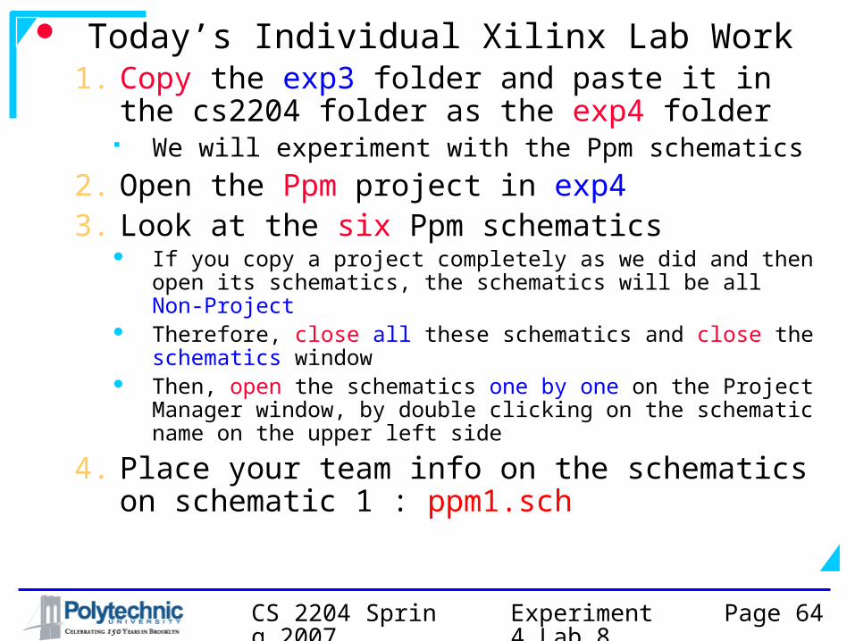
Today’s Individual Xilinx Lab Work1. Copy the exp3 folder and paste it in the
cs2204 folder as the exp4 folder We will experiment with the Ppm schematics
2. Open the Ppm project in exp43. Look at the six Ppm schematics
If you copy a project completely as we did and then open its schematics, the schematics will be all Non-Project
Therefore, close all these schematics and close the schematics window
Then, open the schematics one by one on the Project Manager window, by double clicking on the schematic name on the upper left side
4. Place your team info on the schematics on schematic 1 : ppm1.sch
Experiment 4 Lab 8
CS 2204 Spring 2007
Page 65
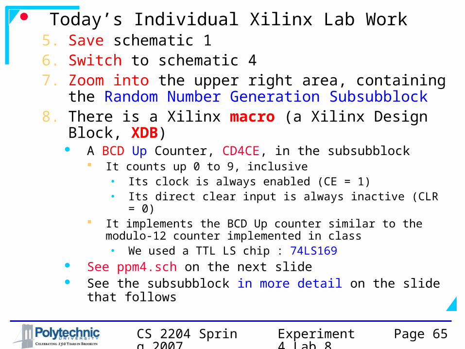
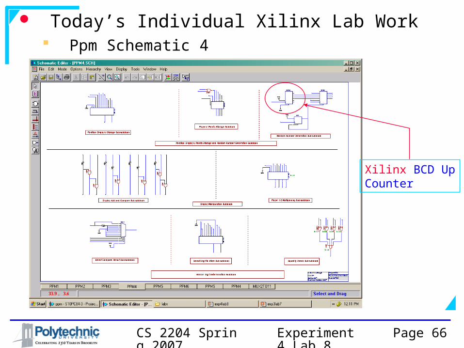
Today’s Individual Xilinx Lab Work5. Save schematic 16. Switch to schematic 47. Zoom into the upper right area, containing the
Random Number Generation Subsubblock8. There is a Xilinx macro (a Xilinx Design Block,
XDB) A BCD Up Counter, CD4CE, in the subsubblock
It counts up 0 to 9, inclusive• Its clock is always enabled (CE = 1)• Its direct clear input is always inactive (CLR = 0)
It implements the BCD Up counter similar to the modulo-12 counter implemented in class• We used a TTL LS chip : 74LS169
See ppm4.sch on the next slide See the subsubblock in more detail on the slide that
follows
Experiment 4 Lab 8
CS 2204 Spring 2007
Page 66
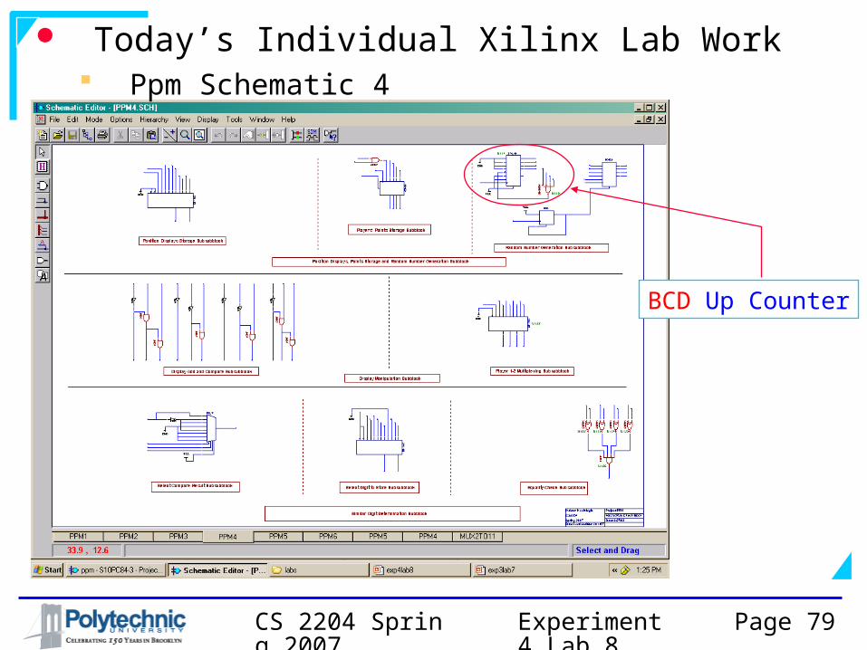
Today’s Individual Xilinx Lab Work Ppm Schematic 4
Xilinx BCD UpCounter
Experiment 4 Lab 8
CS 2204 Spring 2007
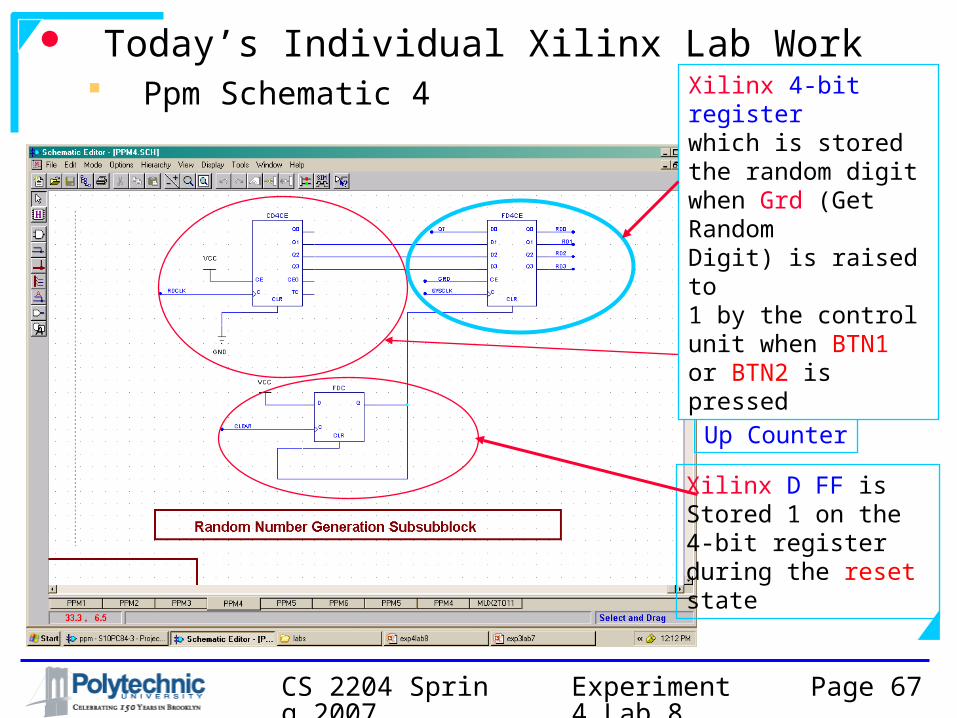
Page 67
Today’s Individual Xilinx Lab Work Ppm Schematic 4
Xilinx BCDUp Counter
Xilinx 4-bit register which is stored the random digit when Grd (Get RandomDigit) is raised to1 by the controlunit when BTN1or BTN2 is pressed
Xilinx D FF is Stored 1 on the 4-bit register during the reset state

Experiment 4 Lab 8
CS 2204 Spring 2007
Page 68
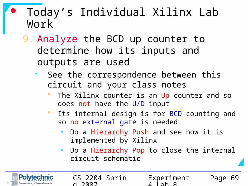
Today’s Individual Xilinx Lab Work9. Analyze the BCD up counter to determine how
its inputs and outputs are used It counts up at the rate of Rdclk (Random digit clock)
Rdclk is generated in the Timing Subblock of schematic 2 It is derived from Q0 which is one of the outputs of a
16-bit Xilinx binary counter, CB16CE, U63 Q0 has the frequency of 192 Hz
Three outputs of the counter are stored on a Xilinx 4-bit register The counter value is stored as the random digit when
Grd (Get random digit) is 1 The rightmost output of the counter is not stored on
the register ! If this output is connected to the register, the
random digit is always odd (1, 3, 5, 7 and 9) It is a problem of the Xilinx software and so to get
around it the register is connected Q7 from U63 in schematic 2
Experiment 4 Lab 8
CS 2204 Spring 2007
Page 69
Today’s Individual Xilinx Lab Work9. Analyze the BCD up counter to
determine how its inputs and outputs are used
See the correspondence between this circuit and your class notes The Xilinx counter is an Up counter and so does not
have the U/D input Its internal design is for BCD counting and so no
external gate is needed• Do a Hierarchy Push and see how it is
implemented by Xilinx• Do a Hierarchy Pop to close the internal circuit
schematic
Experiment 4 Lab 8
CS 2204 Spring 2007
Page 70
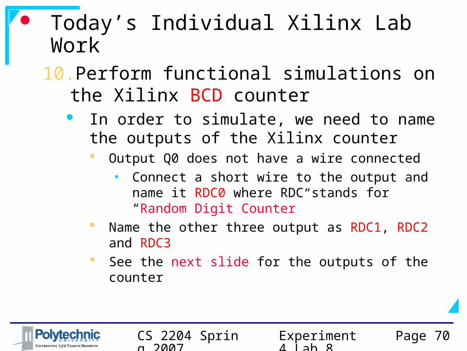
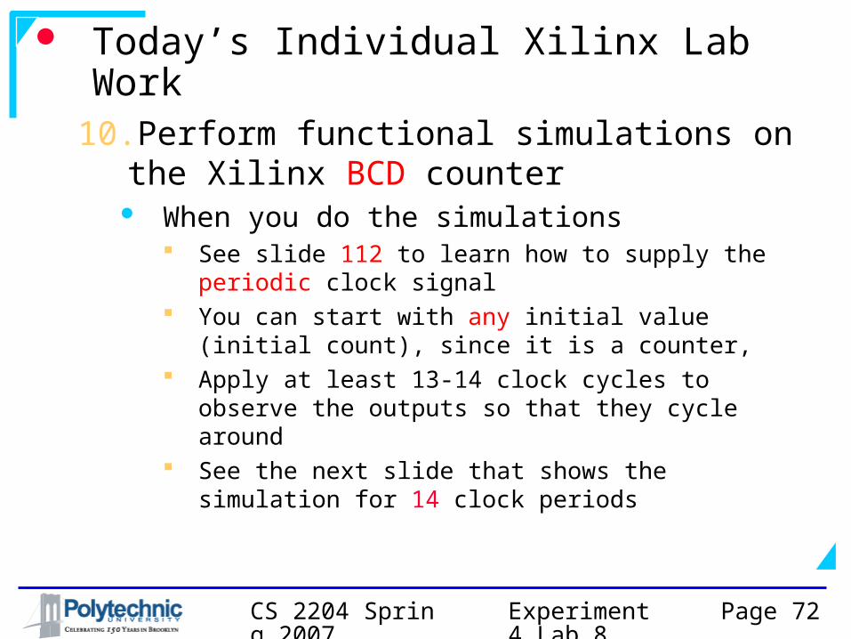
Today’s Individual Xilinx Lab Work10.Perform functional simulations on the
Xilinx BCD counter In order to simulate, we need to name the
outputs of the Xilinx counter Output Q0 does not have a wire connected
• Connect a short wire to the output and name it RDC0 where RDC stands for “Random Digit Counter”
Name the other three output as RDC1, RDC2 and RDC3
See the next slide for the outputs of the counter
Experiment 4 Lab 8
CS 2204 Spring 2007
Page 71
Today’s Individual Xilinx Lab Work Ppm Schematic 4
Experiment 4 Lab 8
CS 2204 Spring 2007
Page 72
Today’s Individual Xilinx Lab Work10.Perform functional simulations on the
Xilinx BCD counter When you do the simulations
See slide 112 to learn how to supply the periodic clock signal
You can start with any initial value (initial count), since it is a counter,
Apply at least 13-14 clock cycles to observe the outputs so that they cycle around
See the next slide that shows the simulation for 14 clock periods
Experiment 4 Lab 8
CS 2204 Spring 2007
Page 73
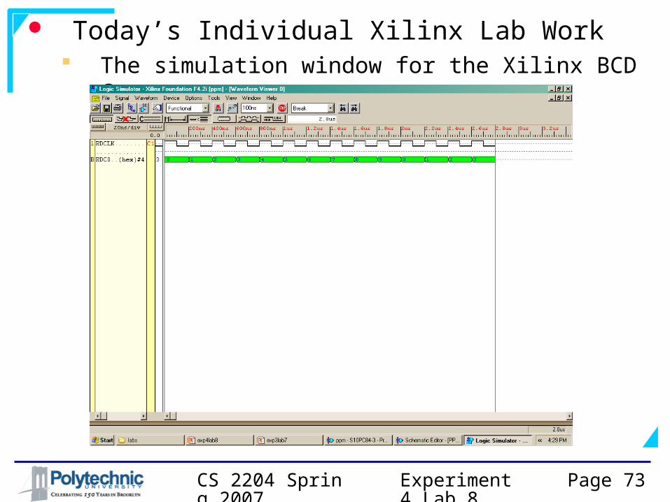
Today’s Individual Xilinx Lab Work The simulation window for the Xilinx BCD
Counter
Experiment 4 Lab 8
CS 2204 Spring 2007
Page 74
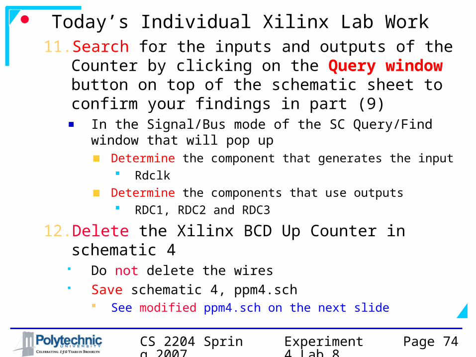
Today’s Individual Xilinx Lab Work11. Search for the inputs and outputs of the
Counter by clicking on the Query window button on top of the schematic sheet to confirm your findings in part (9)
In the Signal/Bus mode of the SC Query/Find window that will pop up
Determine the component that generates the input Rdclk
Determine the components that use outputs RDC1, RDC2 and RDC3
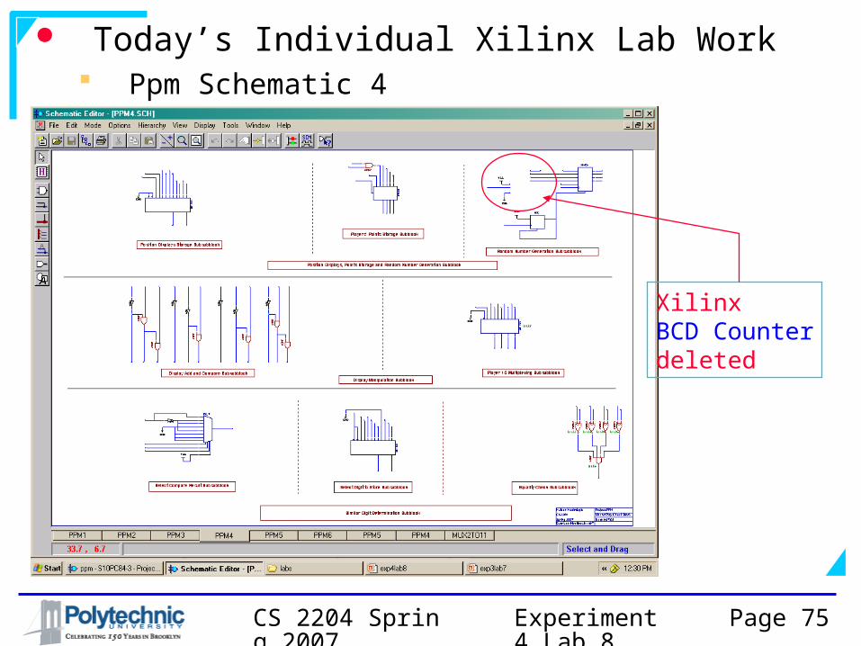
12. Delete the Xilinx BCD Up Counter in schematic 4
Do not delete the wires Save schematic 4, ppm4.sch
See modified ppm4.sch on the next slide
Experiment 4 Lab 8
CS 2204 Spring 2007
Page 75
Today’s Individual Xilinx Lab Work Ppm Schematic 4
XilinxBCD Counterdeleted
Experiment 4 Lab 8
CS 2204 Spring 2007
Page 76
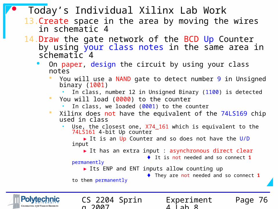
Today’s Individual Xilinx Lab Work13. Create space in the area by moving the wires in
schematic 414. Draw the gate network of the BCD Up Counter
by using your class notes in the same area in schematic 4
On paper, design the circuit by using your class notes You will use a NAND gate to detect number 9 in Unsigned
binary (1001)• In class, number 12 in Unsigned Binary (1100) is detected
You will load (0000) to the counter• In class, we loaded (0001) to the counter
Xilinx does not have the equivalent of the 74LS169 chip used in class• Use, the closest one, X74_161 which is equivalent to the
74LS161 4-bit Up counter ► It is an Up Counter and so does not have the U/D input ► It has an extra input : asynchronous direct clear It is not needed and so connect 1 permanently ► Its ENP and ENT inputs allow counting up They are not needed and so connect 1 to them permanently
Experiment 4 Lab 8
CS 2204 Spring 2007
Page 77
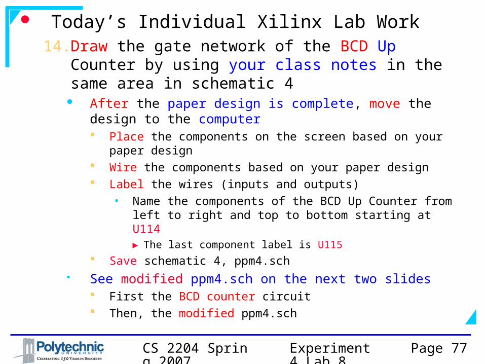
Today’s Individual Xilinx Lab Work14. Draw the gate network of the BCD Up Counter
by using your class notes in the same area in schematic 4
After the paper design is complete, move the design to the computer Place the components on the screen based on your paper
design Wire the components based on your paper design Label the wires (inputs and outputs)
• Name the components of the BCD Up Counter from left to right and top to bottom starting at U114
► The last component label is U115
Save schematic 4, ppm4.sch See modified ppm4.sch on the next two slides
First the BCD counter circuit Then, the modified ppm4.sch
Experiment 4 Lab 8
CS 2204 Spring 2007
Page 78
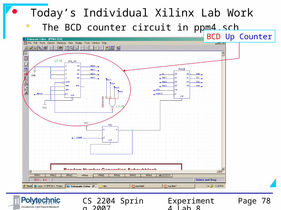
Today’s Individual Xilinx Lab Work The BCD counter circuit in ppm4.sch
BCD Up Counter
Experiment 4 Lab 8
CS 2204 Spring 2007
Page 79
Today’s Individual Xilinx Lab Work Ppm Schematic 4
BCD Up Counter
Experiment 4 Lab 8
CS 2204 Spring 2007
Page 80
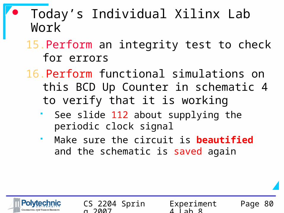
Today’s Individual Xilinx Lab Work15.Perform an integrity test to check for
errors16.Perform functional simulations on this
BCD Up Counter in schematic 4 to verify that it is working
See slide 112 about supplying the periodic clock signal
Make sure the circuit is beautified and the schematic is saved again
Experiment 4 Lab 8
CS 2204 Spring 2007
Page 81
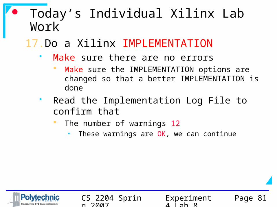
Today’s Individual Xilinx Lab Work17.Do a Xilinx IMPLEMENTATION
Make sure there are no errors Make sure the IMPLEMENTATION options are
changed so that a better IMPLEMENTATION is done Read the Implementation Log File to confirm
that The number of warnings 12
• These warnings are OK, we can continue
Experiment 4 Lab 8
CS 2204 Spring 2007
Page 82
Today’s Individual Xilinx Lab Work17.Do a Xilinx IMPLEMENTATION
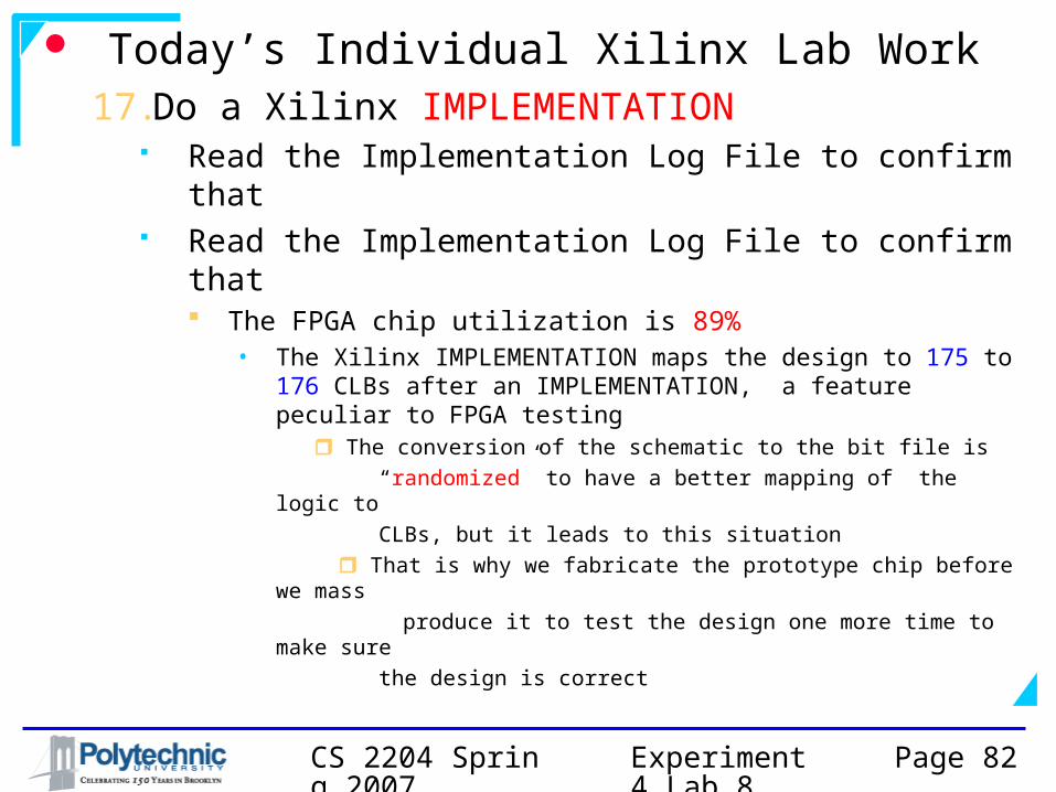
Read the Implementation Log File to confirm that
Read the Implementation Log File to confirm that The FPGA chip utilization is 89%
• The Xilinx IMPLEMENTATION maps the design to 175 to 176 CLBs after an IMPLEMENTATION, a feature peculiar to FPGA testing The conversion of the schematic to the bit file is “randomized” to have a better mapping of the logic to CLBs, but it leads to this situation
That is why we fabricate the prototype chip before we mass
produce it to test the design one more time to make sure the design is correct

Experiment 4 Lab 8
CS 2204 Spring 2007
Page 83
Today’s Individual Xilinx Lab Work18. Download the Ppm project to the FPGA chip and
play the game and to verify that the schematic works correctly
If it does not work, inspect your circuit in Block 4 and correct your circuit
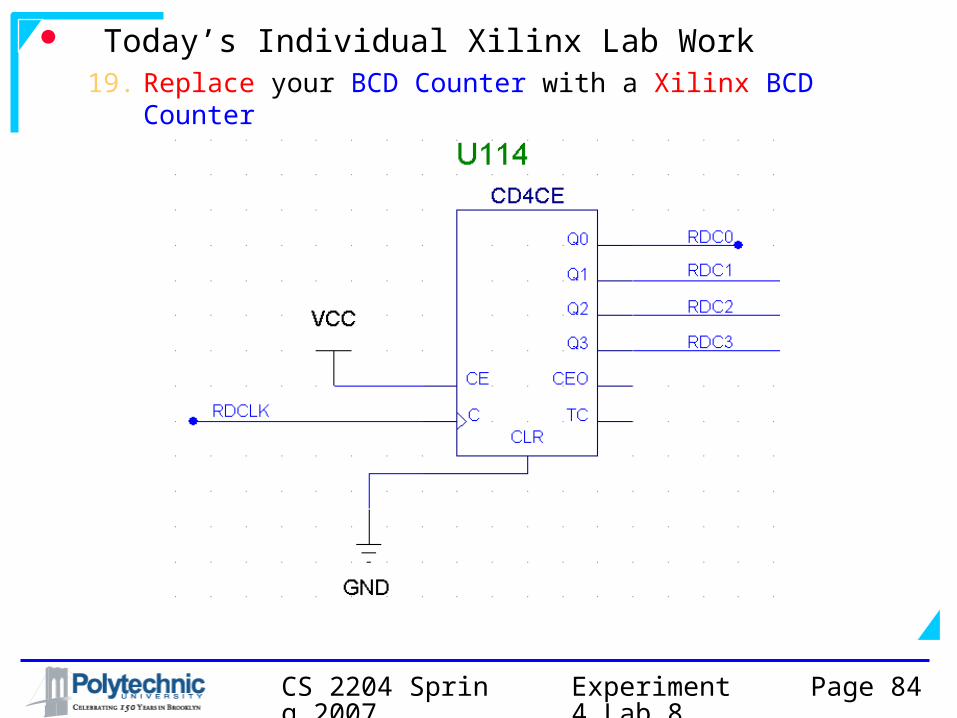
19. Replace your BCD Counter with a Xilinx BCD Counter
It is a Xilinx CD4CE componentConnect its input and outputsLabel it as U114See modified ppm4.sch on the next slide
Do a Xilinx IMPLEMENTATIONDownload the ppm project to the FPGA chip and play the game and to verify that it works correctly
Experiment 4 Lab 8
CS 2204 Spring 2007
Page 84
Today’s Individual Xilinx Lab Work19. Replace your BCD Counter with a Xilinx BCD Counter

Experiment 4 Lab 8
CS 2204 Spring 2007
Page 85
Today’s Individual Xilinx Lab Work20. Read slides on the Ppm, Project Manager,
Schematic design and other related topics at the end
21. Help your partners complete today’s project22. Continue reading the Term Project handout
Move circuits in Blocks 3, 4, 5 and 6 to their appropriate places In Experiments 2, 3 and 4
After all circuits are in their proper places, label the components Last Xilinx component label in Block 5 : U150
If necessary, download the other two versions of the term project to refresh your memory• Ppm human vs. human : ppmhvsh• Ppm machine vs. machine : ppmmvsm
Experiment 4 Lab 8
CS 2204 Spring 2007
Page 86
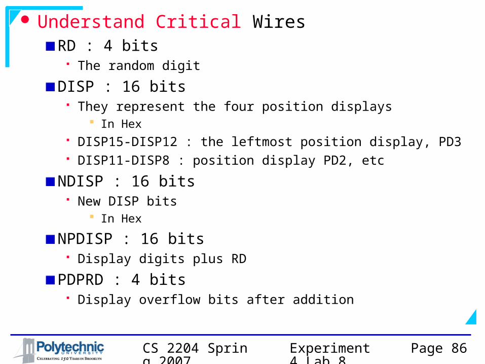
Understand Critical WiresRD : 4 bits
The random digit
DISP : 16 bits They represent the four position displays
In Hex DISP15-DISP12 : the leftmost position display, PD3 DISP11-DISP8 : position display PD2, etc
NDISP : 16 bits New DISP bits
In Hex
NPDISP : 16 bits Display digits plus RD
PDPRD : 4 bits Display overflow bits after addition
Experiment 4 Lab 8
CS 2204 Spring 2007
Page 87
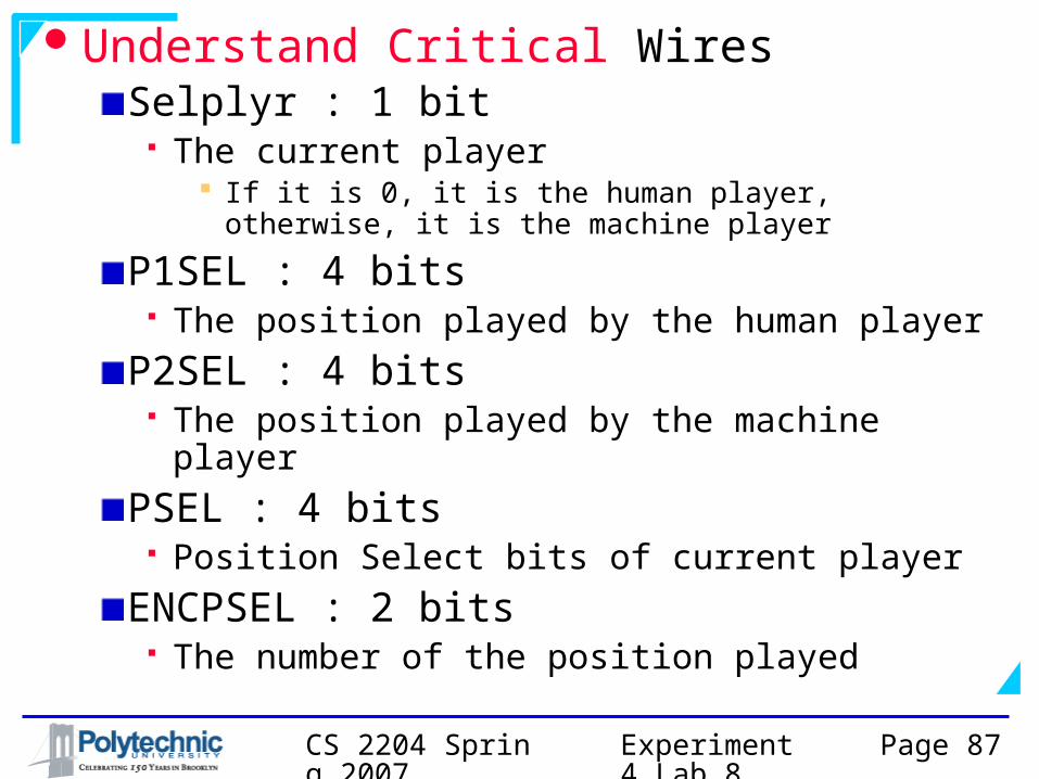
Understand Critical WiresSelplyr : 1 bit
The current player If it is 0, it is the human player, otherwise, it is the
machine player
P1SEL : 4 bits The position played by the human player
P2SEL : 4 bits The position played by the machine player
PSEL : 4 bits Position Select bits of current player
ENCPSEL : 2 bits The number of the position played
Experiment 4 Lab 8
CS 2204 Spring 2007
Page 88
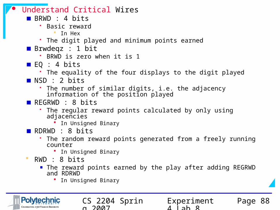
Understand Critical WiresBRWD : 4 bits
Basic reward In Hex
The digit played and minimum points earnedBrwdeqz : 1 bit
BRWD is zero when it is 1EQ : 4 bits
The equality of the four displays to the digit playedNSD : 2 bits
The number of similar digits, i.e. the adjacency information of the position played
REGRWD : 8 bits The regular reward points calculated by only using adjacencies
In Unsigned Binary
RDRWD : 8 bits The random reward points generated from a freely running counter
In Unsigned Binary RWD : 8 bits
The reward points earned by the play after adding REGRWD and RDRWD
In Unsigned Binary
Experiment 4 Lab 8
CS 2204 Spring 2007
Page 89
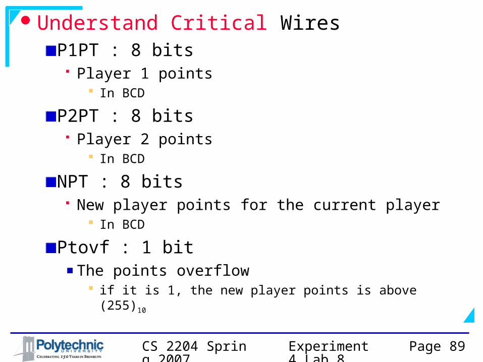
Understand Critical WiresP1PT : 8 bits
Player 1 points In BCD
P2PT : 8 bits Player 2 points
In BCD
NPT : 8 bits New player points for the current player
In BCD
Ptovf : 1 bitThe points overflow
if it is 1, the new player points is above (255)10
Experiment 4 Lab 8
CS 2204 Spring 2007
Page 90
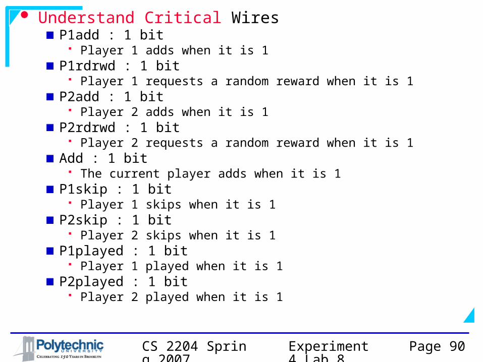
Understand Critical WiresP1add : 1 bit
Player 1 adds when it is 1P1rdrwd : 1 bit
Player 1 requests a random reward when it is 1P2add : 1 bit
Player 2 adds when it is 1P2rdrwd : 1 bit
Player 2 requests a random reward when it is 1Add : 1 bit
The current player adds when it is 1P1skip : 1 bit
Player 1 skips when it is 1P2skip : 1 bit
Player 2 skips when it is 1P1played : 1 bit
Player 1 played when it is 1P2played : 1 bit
Player 2 played when it is 1

Experiment 4 Lab 8
CS 2204 Spring 2007
Page 91
Understand Critical WiresClear : 1 bit
Clear FFs, registers, counters, etc. during reset in Block 2 and Block 4 so that it can play again
Clearp2ffs : 1 bit Clears Player 2 FFs, counters and registers
Clff : 1 bit Clears FFs in Block 2 so that the next player can play if there is no
overflowStp1pt : 1 bit
Store Player 1 pointsStp2pt : 1 bit
Store Player 2 pointsRdrwdsel : 1 bit
Current player has requested a random reward when it is 1Sysclk : 1 bit
System clock of the operation diagram at 6 Hz to the digit playedS1 : 1 bit
State 1 where when it is 1, the Ppm is in state 1S4 : 1 bit
State 4 where when it is 1, the Ppm is in state 4
Experiment 4 Lab 8
CS 2204 Spring 2007
Page 92
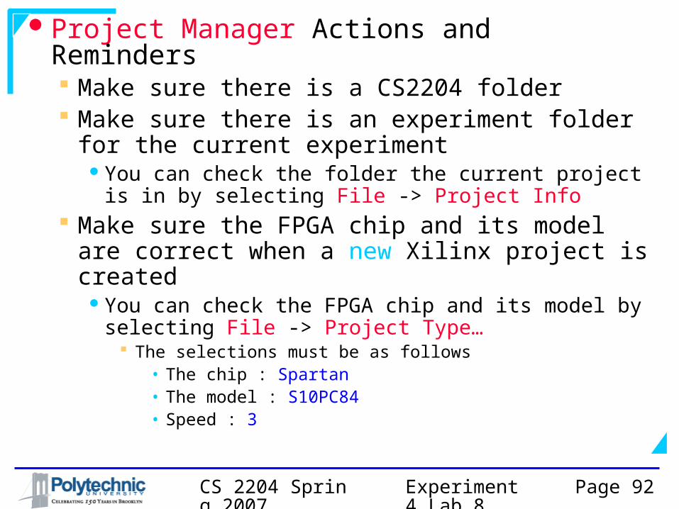
Project Manager Actions and Reminders Make sure there is a CS2204 folder Make sure there is an experiment folder for
the current experimentYou can check the folder the current project is in
by selecting File -> Project Info Make sure the FPGA chip and its model are
correct when a new Xilinx project is createdYou can check the FPGA chip and its model by
selecting File -> Project Type… The selections must be as follows
• The chip : Spartan • The model : S10PC84• Speed : 3
Experiment 4 Lab 8
CS 2204 Spring 2007
Page 93
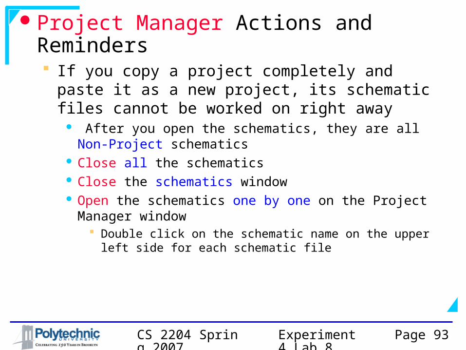
Project Manager Actions and Reminders If you copy a project completely and paste it as a
new project, its schematic files cannot be worked on right away
After you open the schematics, they are all Non-Project schematics
Close all the schematics Close the schematics window Open the schematics one by one on the Project
Manager window Double click on the schematic name on the upper left side
for each schematic file

Experiment 4 Lab 8
CS 2204 Spring 2007
Page 94
Project Manager Actions and Reminders When you do the first Xilinx
IMPLEMENTATION or after clearing the implementation data, you need to change implementation options before clicking on “Run” in the Implement Design Window
You can change the options by selecting Options… in the same window and then
Increase the Place & Route Level to the Highest Effort on the “Options” window
Click on the Edit Options… button for Implementation: in the Program Options area of the “Options” window
Click on Place and Route on the “Spartan Implementation Options: Default” window
Increase Router Options to 5 and 5 for both Routing Passes and Delay-Based Cleanup Passes
Experiment 4 Lab 8
CS 2204 Spring 2007
Page 95
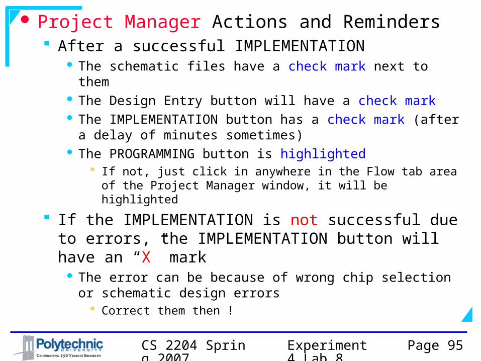
Project Manager Actions and Reminders After a successful IMPLEMENTATION
The schematic files have a check mark next to them The Design Entry button will have a check mark The IMPLEMENTATION button has a check mark (after a
delay of minutes sometimes) The PROGRAMMING button is highlighted
If not, just click in anywhere in the Flow tab area of the Project Manager window, it will be highlighted
If the IMPLEMENTATION is not successful due to errors, the IMPLEMENTATION button will have an “X” mark
The error can be because of wrong chip selection or schematic design errors
Correct them then !
Experiment 4 Lab 8
CS 2204 Spring 2007
Page 96
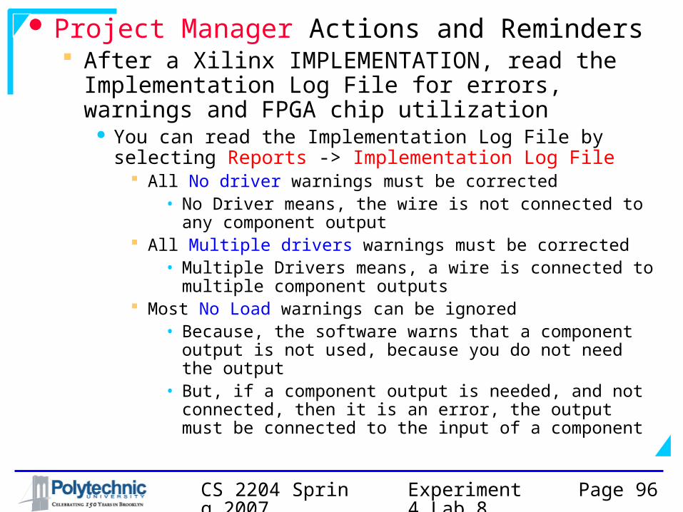
Project Manager Actions and Reminders After a Xilinx IMPLEMENTATION, read the
Implementation Log File for errors, warnings and FPGA chip utilization
You can read the Implementation Log File by selecting Reports -> Implementation Log File
All No driver warnings must be corrected• No Driver means, the wire is not connected to any
component output All Multiple drivers warnings must be corrected
• Multiple Drivers means, a wire is connected to multiple component outputs
Most No Load warnings can be ignored• Because, the software warns that a component output
is not used, because you do not need the output• But, if a component output is needed, and not
connected, then it is an error, the output must be connected to the input of a component
Experiment 4 Lab 8
CS 2204 Spring 2007
Page 97
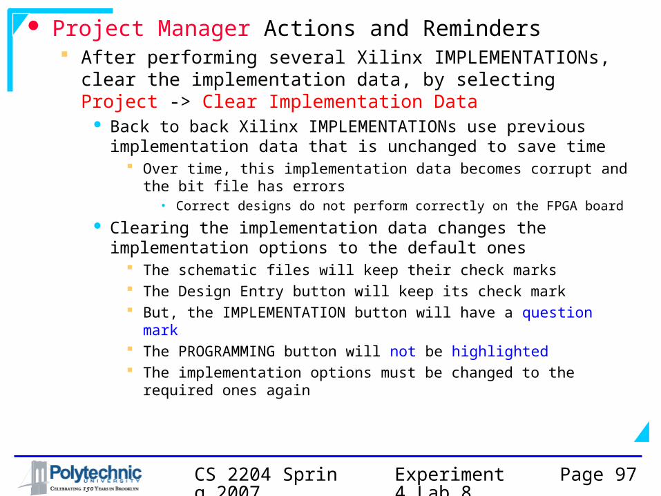
Project Manager Actions and Reminders After performing several Xilinx IMPLEMENTATIONs, clear
the implementation data, by selecting Project -> Clear Implementation Data
Back to back Xilinx IMPLEMENTATIONs use previous implementation data that is unchanged to save time
Over time, this implementation data becomes corrupt and the bit file has errors
• Correct designs do not perform correctly on the FPGA board
Clearing the implementation data changes the implementation options to the default ones
The schematic files will keep their check marks The Design Entry button will keep its check mark But, the IMPLEMENTATION button will have a question mark The PROGRAMMING button will not be highlighted The implementation options must be changed to the required
ones again
Experiment 4 Lab 8
CS 2204 Spring 2007
Page 98
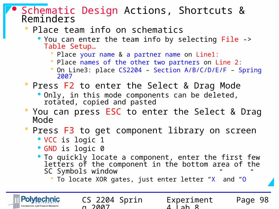
Schematic Design Actions, Shortcuts & Reminders Place team info on schematics
You can enter the team info by selecting File -> Table Setup…
Place your name & a partner name on Line1: Place names of the other two partners on Line 2: On Line3: place CS2204 – Section A/B/C/D/E/F – Spring 2007
Press F2 to enter the Select & Drag Mode Only, in this mode components can be deleted, rotated,
copied and pasted You can press ESC to enter the Select & Drag Mode Press F3 to get component library on screen
VCC is logic 1 GND is logic 0 To quickly locate a component, enter the first few letters
of the component in the bottom area of the SC Symbols window
To locate XOR gates, just enter letter “X” and “O”
Experiment 4 Lab 8
CS 2204 Spring 2007
Page 99
Schematic Design Actions, Shortcuts & Reminders Press F4 to draw wires Press F5 to draw buses Press F7 to search for wires and components
To search for wires, select the Signal/Bus mode If the wire does not have a name, the software assigns one
that starts with a “$” symbol and ends with a “_” symbol• Use the whole name to search for a wire
To search for a component, select the Instance mode If a component does not have a name, the software assigns
one that starts with “$I” symbols followed by a number• Use the whole name to search for the component
Press F8 to start simulation quickly Press F10 to refresh the screen
Experiment 4 Lab 8
CS 2204 Spring 2007
Page 100
Schematic Design Actions, Shortcuts & Reminders Press ctrl-c to copy a wire or a component selected
When components are copied, their labels are not copied !
You can copy from a schematic that belongs to another project
To open the schematic of another project, click on button in the upper left corner, then select the schematic file which will be in another folder
Press ctrl-v to paste a wire or a component Press ctrl-r/ctrl-l to rotate components right/left
Wires cannot be rotated ! You can see how a Xilinx macro is designed (the
internal structure), do a Hierarchy Push, by selecting Hierarchy -> Hierarchy Push
You can close the macro internal design screen, by selecting Hierarchy -> Hierarchy Pop

Experiment 4 Lab 8
CS 2204 Spring 2007
Page 101
Schematic Design Actions, Shortcuts & Reminders Unless otherwise stated, use Xilinx macros instead of
designing them to save time Use buffers to rename wires Do not use unnecessary input/output buffers Do not use unnecessary input/output pads If you copy and paste components, their labels are not
copied and pasted by the software You will need to “source” the schematic file to copy and paste
component labels as explained in the Advanced Xilinx and Digilent Features handout
Xilinx does not have high density ROM memory components
16x1-bit and 32x1-bit They may not be used at all
• If needed, its usage is described on page 9 of the Advanced Xilinx and Digilent Features handout
Experiment 4 Lab 8
CS 2204 Spring 2007
Page 102
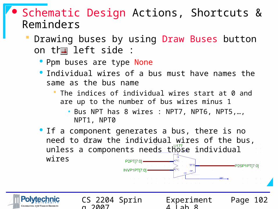
Schematic Design Actions, Shortcuts & Reminders Drawing buses by using Draw Buses button on
the left side : Ppm buses are type None Individual wires of a bus must have names the same as
the bus name The indices of individual wires start at 0 and are up to the
number of bus wires minus 1• Bus NPT has 8 wires : NPT7, NPT6, NPT5,…, NPT1,
NPT0 If a component generates a bus, there is no need to
draw the individual wires of the bus, unless a components needs those individual wires
Experiment 4 Lab 8
CS 2204 Spring 2007
Page 103
Schematic Design Actions, Shortcuts & Reminders Beautify the schematic for documentation
purposes Place components of different sub/blocks separate from
each other to recognize them Write Comments, draw lines and rectangles and label
sub/blocks to identify them on the schematic for documentation purposes
• Use the Graphics Toolbox button on the left : Label components appropriately
Wire names follow application and block partitioning naming requirements
• Except for wires that are connected IBUFs, OBUFs, IPADs and OPADs
Component names start with a U• Except if it is a BUF, IBUF, OBUF, IPAD or OPAD
To label a component, right click on the component and select Symbol Properties…
• Give the name in the Reference: section of the Symbol Properties window
Experiment 4 Lab 8
CS 2204 Spring 2007
Page 104
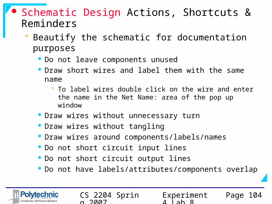
Schematic Design Actions, Shortcuts & Reminders Beautify the schematic for documentation
purposes Do not leave components unused Draw short wires and label them with the same name
To label wires double click on the wire and enter the name in the Net Name: area of the pop up window
Draw wires without unnecessary turn Draw wires without tangling Draw wires around components/labels/names Do not short circuit input lines Do not short circuit output lines Do not have labels/attributes/components overlap
Experiment 4 Lab 8
CS 2204 Spring 2007
Page 105
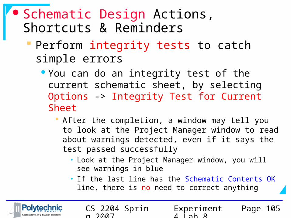
Schematic Design Actions, Shortcuts & Reminders Perform integrity tests to catch simple
errorsYou can do an integrity test of the current
schematic sheet, by selecting Options -> Integrity Test for Current Sheet
After the completion, a window may tell you to look at the Project Manager window to read about warnings detected, even if it says the test passed successfully
• Look at the Project Manager window, you will see warnings in blue
• If the last line has the Schematic Contents OK line, there is no need to correct anything
Experiment 4 Lab 8
CS 2204 Spring 2007
Page 106
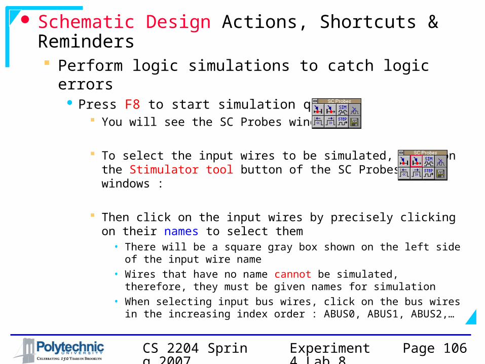
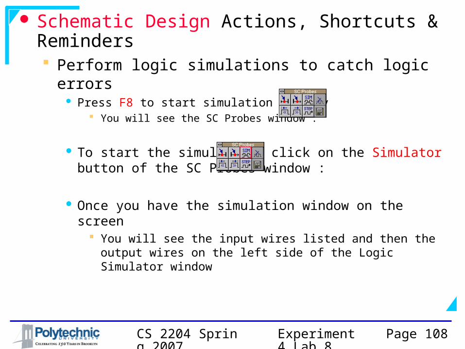
Schematic Design Actions, Shortcuts & Reminders Perform logic simulations to catch logic errors
Press F8 to start simulation quickly You will see the SC Probes window :
To select the input wires to be simulated, click on the Stimulator tool button of the SC Probes windows :
Then click on the input wires by precisely clicking on their names to select them
• There will be a square gray box shown on the left side of the input wire name
• Wires that have no name cannot be simulated, therefore, they must be given names for simulation
• When selecting input bus wires, click on the bus wires in the increasing index order : ABUS0, ABUS1, ABUS2,…
Experiment 4 Lab 8
CS 2204 Spring 2007
Page 107
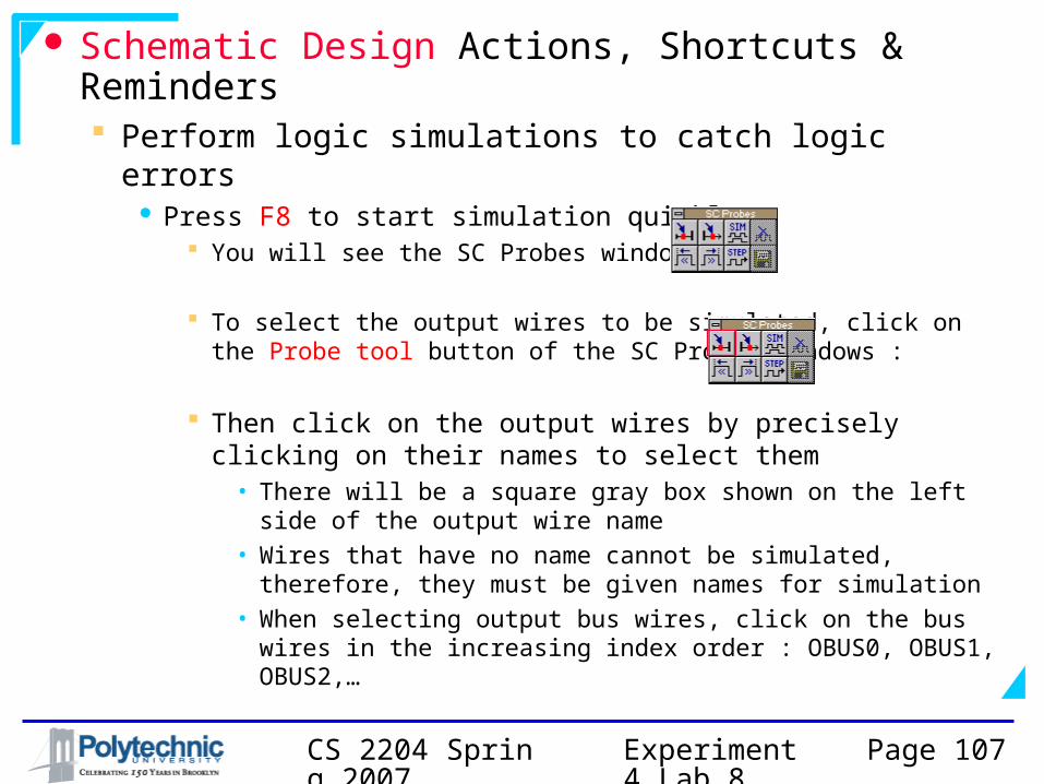
Schematic Design Actions, Shortcuts & Reminders Perform logic simulations to catch logic errors
Press F8 to start simulation quickly You will see the SC Probes window :
To select the output wires to be simulated, click on the Probe tool button of the SC Probes windows :
Then click on the output wires by precisely clicking on their names to select them
• There will be a square gray box shown on the left side of the output wire name
• Wires that have no name cannot be simulated, therefore, they must be given names for simulation
• When selecting output bus wires, click on the bus wires in the increasing index order : OBUS0, OBUS1, OBUS2,…
Experiment 4 Lab 8
CS 2204 Spring 2007
Page 108
Schematic Design Actions, Shortcuts & Reminders Perform logic simulations to catch logic errors
Press F8 to start simulation quickly You will see the SC Probes window :
To start the simulation, click on the Simulator button of the SC Probes window :
Once you have the simulation window on the screen You will see the input wires listed and then the output
wires on the left side of the Logic Simulator window
Experiment 4 Lab 8
CS 2204 Spring 2007
Page 109
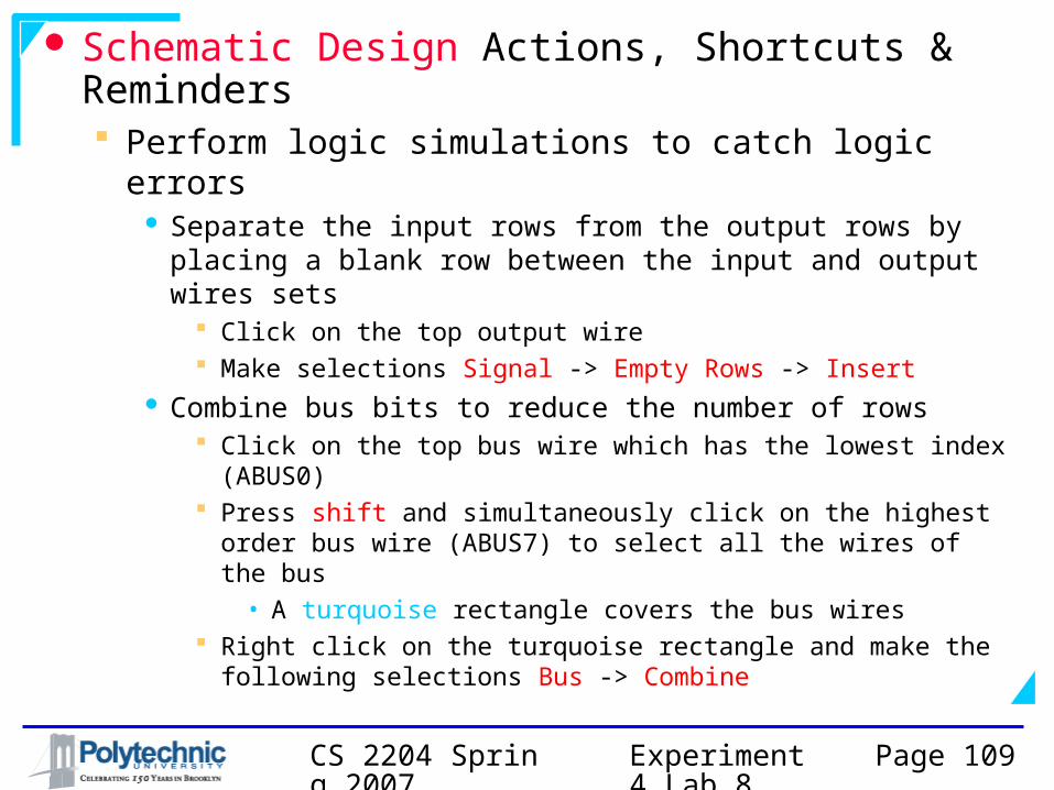
Schematic Design Actions, Shortcuts & Reminders Perform logic simulations to catch logic errors
Separate the input rows from the output rows by placing a blank row between the input and output wires sets
Click on the top output wire Make selections Signal -> Empty Rows -> Insert
Combine bus bits to reduce the number of rows Click on the top bus wire which has the lowest index
(ABUS0) Press shift and simultaneously click on the highest order
bus wire (ABUS7) to select all the wires of the bus• A turquoise rectangle covers the bus wires
Right click on the turquoise rectangle and make the following selections Bus -> Combine
Experiment 4 Lab 8
CS 2204 Spring 2007
Page 110
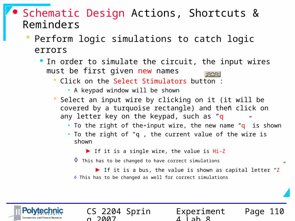
Schematic Design Actions, Shortcuts & Reminders Perform logic simulations to catch logic errors
In order to simulate the circuit, the input wires must be first given new names
Click on the Select Stimulators button : • A keypad window will be shown
Select an input wire by clicking on it (it will be covered by a turquoise rectangle) and then click on any letter key on the keypad, such as “q”
• To the right of the input wire, the new name “q” is shown• To the right of “q”, the current value of the wire is shown
► If it is a single wire, the value is Hi-Z
◊ This has to be changed to have correct simulations
► If it is a bus, the value is shown as capital letter “Z”◊ This has to be changed as well for correct
simulations
Experiment 4 Lab 8
CS 2204 Spring 2007
Page 111
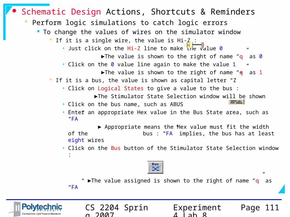
Schematic Design Actions, Shortcuts & Reminders Perform logic simulations to catch logic errors
To change the values of wires on the simulator window If it is a single wire, the value is Hi-Z :
• Just click on the Hi-Z line to make the value 0 ►The value is shown to the right of name “q” as 0• Click on the 0 value line again to make the value 1 ►The value is shown to the right of name “q” as 1
If it is a bus, the value is shown as capital letter “Z”• Click on Logical States to give a value to the bus :
►The Stimulator State Selection window will be shown• Click on the bus name, such as ABUS• Enter an appropriate Hex value in the Bus State area, such as
“FA” ► Appropriate means the Hex value must fit the width of the
bus : “FA” implies, the bus has at least eight wires
• Click on the Bus button of the Stimulator State Selection window :
►The value assigned is shown to the right of name “q” as “FA”

Experiment 4 Lab 8
CS 2204 Spring 2007
Page 112
Schematic Design Actions, Shortcuts & Reminders Perform logic simulations to catch logic errors
To change the values of wires on the simulator window To have a clock signal as an input follow the steps below :
• Make sure the input signal is not renamed as “q”, “w” etc.• Click on the input signal to select it• Click on the Select Stimulators button : • Click on Formula… • Double click on C1: under Clocks• Enter the following in the Edit Formula area :• 100ns=H 100ns=L
► This means a periodic signal which is 100 ns 1 and 100 ns 0 is generated ► The periodic signal has a period of 200ns or a frequency of 5MHz
• Click Accept• Click Close• You will see the C1 button on the Select Stimulators window
highlighted• Click on C1 so that the input signal is renamed C1• Click on the Simulation Step button several times :• You will see the periodic signal automatically generated and
the output values in response to that
Experiment 4 Lab 8
CS 2204 Spring 2007
Page 113
Schematic Design Actions, Shortcuts & Reminders Perform logic simulations to catch logic errors
Start simulating the circuit for different input combinations
If the circuit has 4 or less inputs, then simulate the circuit for all input combinations (test vectors)
• 16 or less number of input combinations (test vectors) If the circuit has more than 4 inputs, select a number of
input combinations (test vectors) then simulate the circuit for these test vectors
• Which test vectors to choose is a very important task ! To simulate the circuit, click on the Simulation Step
button several times : Observe the outputs
If they are correct, try another input combination If wrong, return to the schematic and try to figure out why
it is wrong ! If an output value is Hi-Z or Unknown, there is an error,
correct it
Experiment 4 Lab 8
CS 2204 Spring 2007
Page 114
Schematic Design Actions, Shortcuts & Reminders Printing schematics
1) Double click on the Printer227 icon on your desktop and wait about a minute to allow it to affect the printing option
2) Zoom into an area of the schematic to print the area
3) Select File -> Print on the schematic window4) Change the option to Current View Only on the Print
window5) Click on Setup on the Print Window6) Change the printer to HP Printer 8150 in Room 2277) Click on Options to select Landscape printing if
necessary8) Click OK as many times as needed to print the page9) Print one copy of each area and then make copies
of the printed schematics for your partners
Experiment 4 Lab 8
CS 2204 Spring 2007
Page 115
What to do if the testing on the board gives wrong results even thought the design is correct ?
If the design is absolutely correct, here are the steps to follow in sequence :
1) The FPGA board is turned on ?2) SW9 is in the PROG position ?3) The Bitronics Data Switch selects your PC ?4) The FPGA type and model are correct ?5) The implementation options are changed ?6) There are not too many levels of folders to reach the project
on the PC ?7) Clear the implementation data, close the software, restart
the software and do a new Xilinx IMPLEMENTATION Does it work now ?
8) Save the schematic file worked on in a separate folder Delete the project, recreate the project, copy the schematic
design from the saved schematic file• Does it work ?
Download the zipped project from the course web site, unzip it, copy the schematic design from the saved schematic file• Does it work ?
Experiment 4 Lab 8
CS 2204 Spring 2007
Page 116
What to do if the testing on the board gives wrong results even thought the design is correct ?
9) Repeat step 7, by using your partner’s working schematic
10) Login to another PC and try steps 5 - 811) Ask from the TA to help you
a) The TA will login to your original PC and try steps 5 – 8 by using your schematic design and his/her S drive
b) The TA will login to another PC and try steps 5 – 8 by using your schematic design and his/her S drive on the new PC
c) The TA will inform the professor
12) If the project works on the second PC, inform the lab supervisor, Mr. Keni Yip that the original PC has a problem