cochlea-inspired channelizing filters for wideband radio
TRANSCRIPT

Cochlea-Inspired Channelizing Filters for
Wideband Radio Systems
by
Christopher J. Galbraith
A dissertation submitted in partial fulfillmentof the requirements for the degree of
Doctor of Philosophy(Electrical Engineering)
in The University of Michigan2008
Doctoral Committee:Professor Kamal Sarabandi, Co-ChairProfessor Gabriel M. Rebeiz, Co-Chair, University of California, San DiegoProfessor Karl GroshProfessor Fawwaz T. Ulaby

c© Christopher J. Galbraith
All Rights Reserved
2008

To my family.
ii

Acknowledgements
The completion of this dissertation would not have been possible without the
help and encouragement of many people. First, my advisor Prof. Gabriel Rebeiz
is due immense thanks for his role as my teacher and friend. Working for Gabriel
provides a student with outstanding resources in the form of state-of-the-art labs,
connections to academia and industry, and his own constant technical and moral
support. As important, Gabriel provides an environment and training that places
paramount importance on producing high quality research and achieving deep tech-
nical understanding. I am also thankful to Gabriel for connecting me with so many
aspects of the research community. With his support, I have attended conferences
and visited research laboratories all over the country, enriching my experience of our
profession and inspiring me through exposure to great people and institutions, and
their monumental technical achievements.
I also sincerely thank my other committee members for their interest and valuable
expertise, time, and effort in advising my dissertation work. Prof. Kamal Sarabandi
has been one of my most influential professors, instilling in me the importance of elec-
tromagnetics in all realms of electrical engineering and serving as a remarkable exam-
ple of what one can accomplish when they possess a mastery of both physical concepts
and the underlying mathematics. He is also a very generous and gifted teacher. It is
an honor for me to have him serve as my committee co-chair. Prof. Karl Grosh has
been an invaluable resource in the basic theory and direction of my dissertation re-
search. He has always been eager to offer suggestions and critical advice, and I thank
him for all of his support and encouragement. Finally, I thank Prof. Fawwaz Ulaby
iii
for his interest in my work and for serving on my committee. Prof. Ulaby has had a
profound influence on my education at Michigan through his example as a leader in
research and a world-class educator.
The work in this dissertation got off the ground quickly in large part due to
the cochlear modeling work of Prof. Grosh’s former students Prof. Rob White and
Dr. Lei Cheng. I thank Rob and Lei for their great help and encouragement. In the
EECS Department, I thank Beth Stalnaker and Becky Turanski for their expert and
always-cheerful help in navigating the graduate program, while keeping my funding
and benefits intact. And, I owe many debts to Karla Johnson in the Radiation
Laboratory for the continuous help she provides to all of us Radlab students.
The Radiation Laboratory at The University of Michigan is a wonderful place
for a graduate student, in large part due to the nice and talented people. I am
thankful for my friends there who made research so productive and graduate school
life so much more bearable, and often great fun. In particular, former TICS group
members Dr. Timothy Hancock, Prof. Kamran Entesari, Prof. Abbas Abbaspour-
Tamijani, Dr. Bernhard Schoenlinner, Dr. Bryan Hung, Dr. Tauno Vaha-Heikkila,
Dr. Jad Rizk, and Dr. Andy Brown were outstanding mentors during my first years
in graduate school. Of my contemporaries in Gabriel’s research group at Michigan,
Michael Chang, Carson White, Byung-Wook Min, Sang-June Park, Mohammed El-
Tanani, and Alex Grichener have all been excellent companions, classmates, occa-
sional roommates, as well as technical consultants. For the past two years working
among Gabriel’s new group at the University of California, San Diego, I have been
very fortunate to share a sunny office and gorgeous lab with new friends Tiky Yu,
Jason May, Dr. Bala Lakshminarayanan, Ramadan Al-Halabi, Dr. Jeong-Geun Kim,
Sang-Young Kim, Kwang-Jin Koh, Isak Reines, Berke Cetinoneri, Yusuf Atesal, and
Yu-Chin Ou. The new UCSD students are arriving faster than I can name them, but
I thank them, too, for being excellent office and lab mates.
iv

It is with great pleasure that I acknowledge my favorite distraction at Michigan:
The University of Michigan Amateur Radio Club. Amateur Radio is as old as modern
radio itself (the club was first established at Michigan in 1913) and tends to attract
radio engineers who just can’t get enough hands-on experimentation in their work
or school lives. It also attracts non-engineers which, thankfully, makes for a commu-
nity with wide-ranging interests and expertise and a common fascination with radio.
I’ve had some very fun times at the W8UM “shack” in the EECS building thanks
to the other club members including Jon Suen, Richard French, fellow Radlab-er
Dr. Lora Schulwitz, and many others. And, I am forever grateful to Dean David Mun-
son, Dean Tony England, Prof. Brian Gilchrist, and Adjunct Professor Bill Becher
for their immense support of the club.
Before graduate school, I was fortunate to have two summer internships at TRW
Space and Electronics (now Northrop Grumman Space Technology) that sparked
my interest in filters and multiplexers, gave me excellent experience in monolithic
microwave circuit design, and connected me with a great number of excellent engineers
and wonderful people. I thank Sheila Bloodgood and Dr. Cheng-Chih Yang for these
memorable and defining opportunities.
I would also like to thank several people at M.I.T. Lincoln Laboratory (MIT-LL)
who have given me tremendous support in the last three years of my dissertation
work. I am very grateful to Dr. Mark Gouker for supporting our goals and funding
much of the cochlear channelizer research. While visiting MIT-LL for design reviews
and using their measurement facilities, Rick Drangmeister and Dr. Timothy Hancock
were very helpful (a natural extension of Tim’s role in his Radlab student years).
I also thank Vladimir Bolkhovski for fabricating my circuits in MIT-LL’s precision
multi-chip module process and Peter Murphy for his precise assembly assistance.
Finally, I thank my family. Early on, they must have known that my peculiar
interests might lead to something productive. I thank my Dad for allowing me free
v

reign of the family house’s roof and yards for antenna projects and driving me to
radio stores when I was young. And, I thank my Mom who always encouraged me to
pursue my passion and education. My brother Rob was also encouraging, despite my
routine requests to him (always granted) for help in climbing trees and pruning wire
dipoles. More recently, I thank my sister Anne and brother-in-law Felipe who were
always up for a drive to Ann Arbor for an Indian dinner, and, again my parents who
have always maintained a welcoming house to come home to, especially around the
holidays. I am very grateful to have such a loving and supportive family. Without
them, I surely would not have had the financial and emotional resources to maintain
an extended life as a student.
Chris Galbraith
Ann Arbor, MI
November 12, 2007
vi

Table of Contents
Dedication . . . . . . . . . . . . . . . . . . . . . . . . . . . . . . . . . . . . . ii
Acknowledgements . . . . . . . . . . . . . . . . . . . . . . . . . . . . . . . iii
List of Tables . . . . . . . . . . . . . . . . . . . . . . . . . . . . . . . . . . . ix
List of Figures . . . . . . . . . . . . . . . . . . . . . . . . . . . . . . . . . . x
List of Appendices . . . . . . . . . . . . . . . . . . . . . . . . . . . . . . . . xvi
Chapter 1 Introduction . . . . . . . . . . . . . . . . . . . . . . . . . . . . 11.1 Motivation: Channelization in Radio Systems . . . . . . . . . . . . . 21.2 Multiplexers and Channelizers . . . . . . . . . . . . . . . . . . . . . . 4
1.2.1 Filter and Multiplexer Technologies . . . . . . . . . . . . . . . 51.2.2 Multiplexer Circuit Topologies . . . . . . . . . . . . . . . . . . 61.2.3 Manifold Multiplexer Design and Optimization . . . . . . . . 11
1.3 Research Goals . . . . . . . . . . . . . . . . . . . . . . . . . . . . . . 121.4 Dissertation Overview . . . . . . . . . . . . . . . . . . . . . . . . . . 12
Chapter 2 Cochlear Modeling . . . . . . . . . . . . . . . . . . . . . . . . 142.1 The Mammalian Cochlea . . . . . . . . . . . . . . . . . . . . . . . . . 142.2 One-Dimensional Mechanical Model . . . . . . . . . . . . . . . . . . . 16
2.2.1 An Electrical-Mechanical Analogy . . . . . . . . . . . . . . . . 172.2.2 Non-Uniform Transmission Line Theory . . . . . . . . . . . . 19
Chapter 3 Single-order RF Cochlear Channelizers . . . . . . . . . . . 223.1 Channelizer Circuit Design . . . . . . . . . . . . . . . . . . . . . . . . 22
3.1.1 Constant Fractional Bandwidth Formulation . . . . . . . . . . 233.1.2 Determination of Coefficients . . . . . . . . . . . . . . . . . . 253.1.3 Constant Absolute Bandwidth Formulation . . . . . . . . . . . 283.1.4 Determination of Coefficients . . . . . . . . . . . . . . . . . . 29
3.2 Experimental Results . . . . . . . . . . . . . . . . . . . . . . . . . . . 303.2.1 Constant Fractional Bandwidth Channelizer . . . . . . . . . . 313.2.2 Measurements . . . . . . . . . . . . . . . . . . . . . . . . . . . 323.2.3 Constant Absolute Bandwidth Channelizer . . . . . . . . . . . 353.2.4 Measurements . . . . . . . . . . . . . . . . . . . . . . . . . . . 38
vii

3.3 Channel Filter Properties . . . . . . . . . . . . . . . . . . . . . . . . 423.3.1 Channel Phase Response . . . . . . . . . . . . . . . . . . . . . 423.3.2 Transient Response . . . . . . . . . . . . . . . . . . . . . . . . 423.3.3 Radio System Applications . . . . . . . . . . . . . . . . . . . . 44
Chapter 4 Microwave Planar Cochlear Channelizers . . . . . . . . . . 464.1 Theory . . . . . . . . . . . . . . . . . . . . . . . . . . . . . . . . . . . 474.2 Circuit Design . . . . . . . . . . . . . . . . . . . . . . . . . . . . . . . 484.3 Layout and Fabrication . . . . . . . . . . . . . . . . . . . . . . . . . . 494.4 Results . . . . . . . . . . . . . . . . . . . . . . . . . . . . . . . . . . . 514.5 P-MCM Component Modeling . . . . . . . . . . . . . . . . . . . . . . 57
Chapter 5 Higher-Order Cochlear Channelizers . . . . . . . . . . . . . 645.1 Introduction . . . . . . . . . . . . . . . . . . . . . . . . . . . . . . . . 645.2 Cochlear Channelizers Overview . . . . . . . . . . . . . . . . . . . . . 65
5.2.1 Single-order channelizers . . . . . . . . . . . . . . . . . . . . . 655.2.2 Higher-Order Channelizers . . . . . . . . . . . . . . . . . . . . 66
5.3 Circuit Design . . . . . . . . . . . . . . . . . . . . . . . . . . . . . . . 685.3.1 Design Parameters . . . . . . . . . . . . . . . . . . . . . . . . 685.3.2 Channel Filter Synthesis . . . . . . . . . . . . . . . . . . . . . 685.3.3 Manifold Design . . . . . . . . . . . . . . . . . . . . . . . . . . 75
5.4 Experimental Results . . . . . . . . . . . . . . . . . . . . . . . . . . . 765.4.1 Design, Layout, and Simulation . . . . . . . . . . . . . . . . . 765.4.2 Measurements . . . . . . . . . . . . . . . . . . . . . . . . . . . 825.4.3 Loss Analysis . . . . . . . . . . . . . . . . . . . . . . . . . . . 875.4.4 Power Handling for Transmit Applications . . . . . . . . . . . 87
5.5 Distributed 2nd-order Channelizer Simulations . . . . . . . . . . . . . 895.5.1 Design Equations . . . . . . . . . . . . . . . . . . . . . . . . . 895.5.2 Simulation Results . . . . . . . . . . . . . . . . . . . . . . . . 94
Chapter 6 Conclusion . . . . . . . . . . . . . . . . . . . . . . . . . . . . . 1006.1 Summary of Work . . . . . . . . . . . . . . . . . . . . . . . . . . . . 1006.2 Future Work . . . . . . . . . . . . . . . . . . . . . . . . . . . . . . . . 101
Appendices . . . . . . . . . . . . . . . . . . . . . . . . . . . . . . . . . . . . 103
Bibliography . . . . . . . . . . . . . . . . . . . . . . . . . . . . . . . . . . . 121
viii

List of Tables
Table3.1 Channelizer Center Frequencies (in MHz) . . . . . . . . . . . . . . . . 343.2 Sample Channel Power Distribution for Channel 10 . . . . . . . . . . 373.3 Channelizer Center Frequencies (in MHz) . . . . . . . . . . . . . . . . 393.4 Sample Channel Power Distribution for Channel 10 . . . . . . . . . . 425.1 Measured Channel Characteristics . . . . . . . . . . . . . . . . . . . . 845.2 Sample Channel Power Distribution for Channel 5 . . . . . . . . . . . 875.3 SIR Filter Impedance Definitions . . . . . . . . . . . . . . . . . . . . 92B.1 Transformer Circuit Model Fit Element Values . . . . . . . . . . . . . 120
ix

List of Figures
Figure1.1 Wideband receiver systems: (a) scanning analog superheterodyne, (b)
multi-channel analog superheterodyne, (c) wideband digital, and (d)narrow-band analog or digital with analog preselection. . . . . . . . . 3
1.2 Popular filter technologies used in RF and microwave applications,including multiplexers. . . . . . . . . . . . . . . . . . . . . . . . . . . 7
1.3 Common multiplexer topologies (not including manifold types) usedat RF, microwave, and millimeter-wave frequencies: (a) common portparallel, (b) common port series, (c) channel dropping circulator, (d)channel dropping hybrid, and (e) directional filter. Channel filters (Cn)are standard types with the exception of the directional filters used in(e). . . . . . . . . . . . . . . . . . . . . . . . . . . . . . . . . . . . . . 8
1.4 The manifold multiplexer topology. Channel filters (Cn) are standardtypes, while Mn and Sn are transmission line or waveguide sectionsand Jn are junctions that may also include immittance compensationnetworks such as stubs or lumped-elements. . . . . . . . . . . . . . . 10
1.5 Flow of research from biological inspiration to electrical component. . 122.1 The periphery of the human auditory system. The basilar membrane
is contained within the cochlea. . . . . . . . . . . . . . . . . . . . . . 142.2 (a) The “unwound” basilar membrane acts as a continuum of resonant
beams, shown with input signals of (b) high frequency and (c) lowfrequency. . . . . . . . . . . . . . . . . . . . . . . . . . . . . . . . . . 15
2.3 Discretized transmission line model of the mammalian cochlea. . . . . 182.4 Lumped-element segment used to derive the differential equation de-
scribing a non-uniform transmission transmission line. . . . . . . . . . 193.1 Channelizer S11 for three values of θ. A θ value of 0.9π (b) produces an
input return loss of less than −10 dB over the band from 20–90 MHz.The Smith Chart impedance is 50 Ω. . . . . . . . . . . . . . . . . . . 26
3.2 Schematic diagram of the channelizer prototypes. In this implementa-tion, the resonator capacitances are formed by the parallel combinationof Cfix and Cvar to allow fine tuning. . . . . . . . . . . . . . . . . . . 30
3.3 Photograph of the 20-channel, 20–90 MHz channelizing filter with con-stant fractional bandwidth channels. The inset shows a single channellayout. . . . . . . . . . . . . . . . . . . . . . . . . . . . . . . . . . . . 31
x

3.4 Component values for L1, L2, and C for the 20–90 MHz constant frac-tional bandwidth (8%) channelizer. . . . . . . . . . . . . . . . . . . . 33
3.5 Measured (solid) and simulated (dashed) S11 of the 20-channel constantfractional bandwidth channelizer. . . . . . . . . . . . . . . . . . . . . 34
3.6 Simulated (top) and measured (bottom) S21 for each channel of thechannelizing filter. . . . . . . . . . . . . . . . . . . . . . . . . . . . . 35
3.7 Measured (solid) and simulated (dashed) S21 of the constant fractionalbandwidth channelizer for channels 3 (22.5 MHz), 10 (39.4 MHz), and17 (67.3 MHz). Ripples are due to parasitics and resonances of thelumped components. . . . . . . . . . . . . . . . . . . . . . . . . . . . 36
3.8 Measured power distribution at the center frequency of channel 10(39.4 MHz) among all 20 channels. . . . . . . . . . . . . . . . . . . . 36
3.9 Photograph of the 20-channel, 20–90 MHz channelizing filter with con-stant absolute bandwidth channels. The inset shows a single channellayout. . . . . . . . . . . . . . . . . . . . . . . . . . . . . . . . . . . . 37
3.10 Component values for L1, L2, and C for the 20–90 MHz constant ab-solute bandwidth channelizer. . . . . . . . . . . . . . . . . . . . . . . 38
3.11 Measured (solid) and simulated (dashed) S11 of the 20-channel constantabsolute bandwidth channelizer. . . . . . . . . . . . . . . . . . . . . . 39
3.12 Simulated (top) and measured (bottom) S21 for each channel of theconstant absolute bandwidth channelizing filter. The frequency scaleis linear to show the constant absolute bandwidth response. . . . . . 40
3.13 Measured (solid) and simulated (dashed) S21 of the constant absolutebandwidth channelizer for channels 3 (25.1 MHz), 10 (54.5 MHz), and17 (82.6 MHz). . . . . . . . . . . . . . . . . . . . . . . . . . . . . . . 41
3.14 Measured power distribution at the center of channel 10 (54.5 MHz)among all 20 channels. . . . . . . . . . . . . . . . . . . . . . . . . . . 41
3.15 Measured and simulated phase of S21, at each channel’s center fre-quency, for the constant fractional bandwidth version (top) and theconstant absolute bandwidth version (bottom). The data for eachchannel is taken at the center frequency of the particular channel. . . 43
3.16 The simulated spectrum of the band-limited input signal used in thetime-domain simulation (power adjusted to deliver 0 dBm at the bandcenter). The inset shows the waveforms of pre-filter input monopulse(dashed) and the band-limited signal (solid) that is fed to the channel-izer input. . . . . . . . . . . . . . . . . . . . . . . . . . . . . . . . . . 44
3.17 Three representative simulated waveforms that appear at channelizeroutput ports with the input signal shown in Fig. 3.16. . . . . . . . . . 45
4.1 A spectrum activity monitoring receiver using a channelizing preselec-tor filter. . . . . . . . . . . . . . . . . . . . . . . . . . . . . . . . . . . 46
xi

4.2 (a) Discretized, non-uniform transmission-line model of the basilarmembrane (located within the cochlea). The channelizer is synthe-sized from this model. (b) Integrated channelizing filter schematicdiagram. Trimmer capacitors are used to fine tune resonator centerfrequencies and an L-C matching network transforms the resonatoroutput impedance to 50 Ω. . . . . . . . . . . . . . . . . . . . . . . . . 47
4.3 The Precision Multi-Chip Module (P-MCM) process developed by M.I.T.Lincoln Laboratory. . . . . . . . . . . . . . . . . . . . . . . . . . . . . 50
4.4 A close-up view of the resonator capacitor. The main top plate canbe wire bonded to smaller auxiliary plates to increase capacitance andre-tune the resonator’s center frequency. . . . . . . . . . . . . . . . . 50
4.5 A microphotograph of the 15-channel channelizer. The chip measures3.4 mm by 14.1 mm, not including the microstrip lines leading to probepads (not shown). Channels 1 (furthest from input) and 15 (nearest toinput) are internally terminated in 50 Ω. All other channels are probedusing CPW probe pads (not shown). Diode detectors can be placed ateach channel output for spectrum activity monitoring. . . . . . . . . . 53
4.6 On-wafer S-parameter measurement set-up at M.I.T. Lincoln Labora-tory. A channelizer under test is in the center of the wafer chuck. Fourmulti-port RF probes (total of 14 ports) allow a single two-port channelmeasurement while simultaneously terminated 13 other channels. . . . 54
4.7 Reflection (S11) response of the channelizer, for measured (solid) andsimulated (dashed) results. All channels are terminated in 50 Ω. . . . 55
4.8 Measured transmission (S21) response of channels 2 through 14. . . . 554.9 The transmission (S21) response of the 15 channelizer channels, with
measured (solid) and simulated (dashed) results. Channels 1 and 15were not measured due to a limited number of available wafer probes(these channels are terminated on-chip). . . . . . . . . . . . . . . . . 56
4.10 Suspended P-MCM inductor layout used in Sonnet full-wave simula-tion. Simulation data is de-embedded to the reference planes shownand compared to measured S-parameters. . . . . . . . . . . . . . . . 58
4.11 Simulated (dashed) and measured (solid) inductance of planar spiralinductors in the MIT-LL P-MCM process. L1 is the standard inductorused in the channelizer manifold while L2x are suspended inductorsused in the resonator sections. . . . . . . . . . . . . . . . . . . . . . . 59
4.12 Simulated (dashed) and measured (solid) inductance of the suspendedresonator inductors over their bands of use. . . . . . . . . . . . . . . . 60
4.13 Simulated (dashed) and measured (solid) inductor Q of planar spiralinductors in the MIT-LL P-MCM process. L1 is the standard inductorused in the channelizer manifold while L2x are suspended inductorsused in the resonator sections. . . . . . . . . . . . . . . . . . . . . . . 61
4.14 P-MCM trim-able resonator capacitor layout used in Sonnet full-wavesimulation. Simulation data is de-embedded to the reference planesshown and compared to measured S-parameters. . . . . . . . . . . . . 62
xii

4.15 Simulated (dashed) and measured (solid) capacitance (wide-band, topand narrow-band, middle) and Q (bottom) of a resonator capacitortest structure (Fig. 4.14). . . . . . . . . . . . . . . . . . . . . . . . . . 63
5.1 (a) Single-order cochlear channelizer discretized non-uniform transmis-sion line model. (b) Higher-order channelizer circuit model. . . . . . . 65
5.2 Single channel responses of two channelizers, 3rd-order (solid line)and single-order (dashed line), covering the same bandwidth (200–1000 MHz) with 10, 18% channels. . . . . . . . . . . . . . . . . . . . 67
5.3 Simplified cochlear channelizer schematic at the resonant frequency ofchannel n. . . . . . . . . . . . . . . . . . . . . . . . . . . . . . . . . . 67
5.4 Required channel filter input impedance characteristic (Smith Chart)and the corresponding bandpass filter prototype for a cochlear chan-nelizer (response for 3rd-order shown). . . . . . . . . . . . . . . . . . 69
5.5 Examples of channel filter input impedance characteristics (Smith Charts)and their corresponding bandpass filter prototype (a) and distributedfilter topology (b) which are unsatisfactory for a cochlear channelizer(see text). . . . . . . . . . . . . . . . . . . . . . . . . . . . . . . . . . 70
5.6 Tubular filter topology (3rd-order filter) with lumped-elements. . . . 705.7 Channel filter schematics showing network transformations used to ar-
rive at a channel filter with the desired input impedance characteristics. 725.8 Circuit schematic diagram of a 3rd-order cochlear channelizer. . . . . 765.9 Simulated input impedance of the 10-channel 3rd-order channelizer
without (a) and with (b) the input matching capacitor C0, used tomatch the slightly inductive input impedance. . . . . . . . . . . . . . 77
5.10 Photograph of a 10-channel 3rd-order cochlear channelizer with centerfrequencies ranging from 200 MHz to 1022 MHz. The channel filtersare staggered on the sides of the inductive manifold. The input portis in the center of the lower substrate edge while the two sets of fiveoutput ports occupy the left and right board edges fed by microstriplines from channel outputs. . . . . . . . . . . . . . . . . . . . . . . . . 78
5.11 Close-up photograph (top) of single channel layout identifying a mani-fold inductor Lm (Fig. 5.8) and channel filter circuit components (bot-tom) for channel 5. Ca, Cc, Cd, and Cf are parallel plate capacitorspatterned on the top metal layer, while Cb and Ce are multilayer SMTcapacitors. The three resonator inductors L are air-wound coils whilethe manifold inductance Lm is a 0.635 mm width (100 Ω) microstripline. A 2.54 mm wide 50 Ω microstrip line connects the filter outputto an edge-launch SMA connector (not shown). . . . . . . . . . . . . 79
5.12 Lumped element component values for the 10-channel 200–1000 MHz3rd-order cochlear channelizer (not shown, C0 = 2.75 pF). . . . . . . 80
5.13 Measured (solid) and simulated (dashed) transmission response (Sn,0)of each channel of the 3rd-order cochlear channelizer. . . . . . . . . . 82
5.14 Measured (solid) and simulated (dashed) return loss (S0,0) of the 3rd-order cochlear channelizer. . . . . . . . . . . . . . . . . . . . . . . . . 83
xiii

5.15 Transmission response (top) and group delay (bottom) of channel 5 ofthe 10-channel channelizer (simulated and measured) and the corre-sponding stand-alone 3-pole filter (simulated). . . . . . . . . . . . . . 84
5.16 Measured S1,0 (solid line) along with S1,2...10 (dashed lines) which giveschannel 1’s (n = 1) isolation to other channels (m = 2 . . . 10). Isolationfollows the upper stopband skirt of channel 1 with reduced isolationto channels located on the same side of the manifold (n = 3, 5, 7, 9)(Fig. B.3). . . . . . . . . . . . . . . . . . . . . . . . . . . . . . . . . . 85
5.17 Measured S10,0 (solid line) along with S10,1...9 (dashed lines) which giveschannel 10’s (n = 10) isolation to other channels (m = 1 . . . 9). Isola-tion follows the lower stopband skirt of channel 10 with reduced isola-tion to channels located on the same side of the manifold (n = 2, 4, 6, 8)(Fig. B.3). . . . . . . . . . . . . . . . . . . . . . . . . . . . . . . . . . 86
5.18 Measured rejection of channel 1, 5, and 10 center frequencies at allchannel output ports. . . . . . . . . . . . . . . . . . . . . . . . . . . . 86
5.19 (a) Direct-coupled resonator filter model (N = 2) with ideal invert-ers (Jn,n+1) and parallel resonators (Bk), (b) inverter implementa-tions with transmission lines and a series capacitor, and (c) steppedimpedance resonator (SIR) with equal line lengths. . . . . . . . . . . 91
5.20 Second-order end-coupled λ/2 resonator filters using microstrip (a) uni-form impedance and (b) stepped impedance resonators (SIR). . . . . 91
5.21 Wideband simulated transmission (S21) of 2 GHz filters using constant-impedance (solid line) and stepped impedance (dashed line) resonators. 95
5.22 Simulated transmission (S21) of 2 GHz filters using constant-impedance(solid line) and stepped impedance (dashed line) resonators. . . . . . 95
5.23 Proposed layout for second-order cochlear channelizer using end-coupledstepped-impedance resonator filters. . . . . . . . . . . . . . . . . . . . 96
5.24 Simulated transmission (S21) of each channel of a 2nd-order channelizerusing end-coupled resonator filters (θ01 = 0) at filter input). . . . . . 97
5.25 Simulated transmission (S21) of each channel of a 2nd-order channelizerwith negative transmission line segment at the filter input (θ01 = −22.5). 98
B.1 (a) Lumped-element circuit model of the planar double-tuned trans-former. (b) A real transformer (0 ≤ k ≤ 1) equivalent circuit; thetransformer in this model is ideal (k = 1) with a turns ratio given by(B.1). (c) When the secondary of the double-tuned transformer (a)is resonant, the primary sees the transformed secondary resistance inseries with an inductive reactance; this leakage inductance acts as partof an L-C step-up matching network along with C1. . . . . . . . . . . 113
B.2 The Precision Multi-Chip Module (P-MCM) process developed by M.I.T.Lincoln Laboratory. . . . . . . . . . . . . . . . . . . . . . . . . . . . . 117
B.3 Die photograph of the double-tuned transformer. Capacitors C1 andC2 are not visible below the top metal layer. The backside etching isalso not visible as its outline is covered by the remaining ground plane(partial removal of the ground plane layer results in the black rectanglesurrounding the transformer windings). . . . . . . . . . . . . . . . . . 118
xiv

B.4 Measured, simulated, and model fit response of the double-tuned trans-former circuit. The primary (RS) is terminated in 50 Ω while thesecondary (RL) is terminated in 12.5 Ω. . . . . . . . . . . . . . . . . . 118
B.5 Wideband response of the double-tuned transformer. . . . . . . . . . 119
xv

List of Appendices
AppendixA Channelizer Design Code . . . . . . . . . . . . . . . . . . . . . . . . . 104B Planar Low-Loss Double-Tuned Transformers . . . . . . . . . . . . . . 111B.1 Modeling and Design Trade-Offs . . . . . . . . . . . . . . . . . . . . . 112B.2 Design, Fabrication, and Results . . . . . . . . . . . . . . . . . . . . . 115B.3 Conclusion . . . . . . . . . . . . . . . . . . . . . . . . . . . . . . . . . 119
xvi

Chapter 1
Introduction
Wireless technology has advanced rapidly in the past 120 years. We have come
a long way since the discovery of propagating electromagnetic waves by Maxwell’s
theoretical genius and the experimental work of Hertz and Tesla, and many others.
The broadcast radio, and later, satellite telecommunications industries have provided
steady technological development, while the war time and military applications have
since fueled astonishing radio engineering advancements in short periods of time.
Today, we are very fortunate to have access to a vast amount of well-developed theory.
This, combined with modern electronic fabrication methods and materials, makes
wireless engineering and technology a very mature, rewarding, and exciting pursuit.
Even with so much progress, problems remain without adequate solutions. Ana-
lytical formulations are found for some problems, either due to their simple nature but
often by virtue of workers’ extremely hard work and uncommon insight. Since com-
puters have become available, many problems that have defied attempts at analytical
solution have become solvable through computer-programmed brute force solution
or with the assistance of computer aided design (CAD) tools. Even after applying
all known theory and available computing resources, some problems persist and call
for, at least in part, other means of solution. In this dissertation, one such problem
is approached by means of a biological inspiration. In the course of its solution, the
theory and practice developed by many people in scientific and engineering disciplines
is gratefully used along with computer tools, but, credit for the end product’s most
1

basic structure is due to Nature.
1.1 Motivation: Channelization in Radio Systems
Many commercial and military radio systems depend on channelization, where a
signal is subdivided into several signals, each with a smaller bandwidth. This pro-
cess is also called multiplexing and can be accomplished with a multiplexing filter, or
multiplexer. Channelization is used in communications systems to allow a receiver,
transmitter, or antenna to simultaneously accommodate multiple signals or channels.
For example, in telecommunications satellite transponders, an input multiplexer is
placed at the uplink antenna port in order to channelize the input frequency band
before each channel is up- or down-converted, routed via a switch matrix and sent
to separate high power amplifiers. Then, the channels are recombined in an output
multiplexer that feeds the downlink antenna [1]. Military applications such as elec-
tronic support measures (ESM) receivers also require channelization. ESM receivers
are used to simultaneously monitor a wide bandwidth and detect and classify signals
with a high probability of interception [2, 3]. A typical unit uses a multiplexer at the
antenna port to channelize the receiver bandwidth. Then, each channel output feeds
a receiver chain and detector whose output provides intercepted signal information to
electronic countermeasure (ECM) systems such as jammers [4]. Especially in airborne
systems, ESM receiver multiplexing filters must be compact and lightweight [5, 6].
Various wideband receiver system block diagrams are shown in Fig. 1.1. In the
scanning superheterodyne receiver, the local oscillator (LO) frequency is swept, giving
a wide bandwidth of coverage though instantaneous detection occurs only one narrow,
intermediate frequency (IF), bandwidth at a time (Fig. 1.1a). A multi-channel su-
perheterodyne overcomes the narrow-band limitation by placing many receiver front
ends in parallel, but whose improvement in instantaneous bandwidth requires a com-
2

(a)
fLO
Ch (n ∆t f0)
(c)ADC DSP
Ch 1
Ch N
(b)
fLO
Ch 1
fLOfLO
fLO
Ch N
*
*
Channelizer(d)
Ch 1
Ch N
*Analog detector or ADC/DSP
Figure 1.1: Wideband receiver systems: (a) scanning analog superheterodyne, (b)multi-channel analog superheterodyne, (c) wideband digital, and (d)narrow-band analog or digital with analog preselection.
mensurate increase in electronic components and power (Fig. 1.1b). A wideband
direct-conversion digital receiver is realized by converting the received signal to the
digital domain with an analog to digital converter (ADC) with subsequent channel
filtering and detection implemented by digital signal processing (DSP) (Fig. 1.1c).
With conventional Nyquist ADCs, such a system’s instantaneous bandwidth is less
3

than one half of the ADC’s sampling rate (fs/2) to prevent aliasing [7]. Currently,
commercially available ADCs limit a wideband digital receiver’s bandwidth to about
1 GHz. Another simultaneous wideband receiver approach uses an analog channel-
izing filter and either an array of analog receivers or low sampling rate and low-bit
ADCs (Fig.1.1d). In the first case, analog detectors on each channel output provide
instantaneous spectrum activity monitoring. When each detector is replaced with a
relatively low-cost and low-power digital receiver (ADC and DSP chain), this scheme
provides simultaneous detection over the entire receiver bandwidth. Using a technique
called bandpass sampling, where a signal is down-converted during analog-to-digital
conversion, each ADC’s sampling rate must only be twice the channel bandwidth (not
the entire receiver bandwidth). Also, since the channelizer reduces adjacent-channel
interference, the ADC’s spurious-free dynamic range (SFDR) requirement, and thus
number of required bits, is also significantly reduced [8, 9]. The systems using a front-
end channelizing filter promise high receiver performance over a very large bandwidth
in a small size and with low cost.
The human auditory system also relies on channelization. The cochlea, located
within the inner ear is an amazing audio frequency multiplexing filter. It contains
over 3, 000 channels covering a frequency range greater than 1000:1 in a very compact
package. The goal of this work is to apply the basic fluid-dynamic cochlear structure to
the problem of designing wideband radio frequency (RF) and microwave multiplexers.
1.2 Multiplexers and Channelizers
A multiplexer is an N + 1 port device, with a common port and N channel ports.
The common port can be used as a signal input or output. In the input case, the com-
mon port’s signal is sub-divided and sent to the channel (output) ports. In the output
case, the common port carries the combined signals of all channel (input) ports. In-
4
put multiplexers are intended for receiver applications and usually low power levels
(below 1 W), while output multiplexers are used for transmit applications often in
excess of 100 W per channel. Multiplexers with N = 2 and N = 3 are called diplex-
ers and triplexers, respectively. A duplexer is a diplexer that connects a receiver
and transmitter to an antenna at the common port (other duplexers exist that do
not use a multiplexer). Multiplexers with adjacent channel passbands are called con-
tiguous, while those with non-channelized frequency bands (called “guard bands”) in
between channels are called non-contiguous. Input multiplexers with many contigu-
ous channels are often referred to as channelizers due to their usage in channelizer
receiver front-ends [4, 10]. Along with other monumental advances in radio and radar
engineering, the first modern microwave multiplexers were developed at the M.I.T.
Radiation Laboratory during World War II by Fano and Lawson [11, 12]. Since then,
multiplexer theory and design has received significant attention and in 2007 remains
an important field in radio engineering.
Multiplexers are characterized by their electrical parameters including frequency
coverage, input return loss over the covered band, number of channels, whether the
channels are contiguous or non-contiguous, channel-to-channel isolation, power han-
dling, and linearity (usually in terms of intermodulation distortion). Individual mul-
tiplexer channels are further described by their bandwidth, insertion loss, passband
shape, stop-band rejection, and phase response with respect to the common port.
Channel properties are closely related to the channel filters. Non-electrical multi-
plexer characteristics are also important and include physical size and mass, design
procedure complexity, post-fabrication tuning requirements, and fabrication cost.
1.2.1 Filter and Multiplexer Technologies
All multiplexer properties are influenced by the technology used where circuits
are commonly implemented using waveguide, lumped-element, planar (microstrip,
5

stripline, coplanar waveguide) and coaxial transmission lines. Waveguide, dielectric
resonator, and coaxial-based combline or interdigital types have excellent electrical
performance (insertion loss, rejection, isolation, power handling) by virtue of their
low-loss, high quality factor (Q, ranging from 1, 000 to 100, 000) resonators but are
large, heavy, expensive, and require tuning. In applications that require very small
fractional bandwidth channels, low loss, and high power handling, waveguide multi-
plexers are often the only option. Lumped-element and transmission line multiplexers
are small, lightweight, and inexpensive, but have higher insertion loss due to typical
resonator Qs of 100 to 1, 000). Superconducting technologies (mainly applied to pla-
nar and waveguide types) provide large improvements in electrical performance at a
cost of size, mass, cost, and power consumption. In addition, surface acoustic wave
(SAW) filters and multiplexers are used when their high insertion loss can be toler-
ated, and film bulk acoustic wave resonator (FBAR) duplexers have been recently
developed for cellular handsets (at ∼2 GHz). A summary of widely used filter types
and their range of application is shown in Fig. 1.2 (from [13]).
1.2.2 Multiplexer Circuit Topologies
A multiplexer is a collection of separate channel filters and a means of connecting
each filter to a common port. The method of connection must also provide a means of
tuning out interactions among the individual filters. Without such tuning, the filter
responses are altered resulting in distorted channel passbands and poor multiplexer
input return loss [14, 15].
The most common multiplexer circuit topologies include common port (series
and parallel types), channel dropping, directional filters, and manifold multiplexers
(Fig. 1.3).
6

Bulk
Acoustic
SAW
Helical
Coaxial Waveguide
Dielectric
Resonator
Stripline
Center Frequency (GHz)
0.01 0.1 10 100
Fra
ctio
nal
Ban
dw
itdth
10-5
10-4
10-3
10-2
10-1
100
1
Figure 1.2: Popular filter technologies used in RF and microwave applications, in-cluding multiplexers.
7

Rs
vs
C1
C1
3-dB
Hybrid
3-dB
Hybrid R1
C2
C2
3-dB
Hybrid
3-dB
Hybrid R2
CN
CN
3-dB
Hybrid
3-dB
Hybrid RN
Rs
vs
RN
R2
R1
C1
C2
CN
vs R
s
C1
Directional
Filter
R1
C2
Directional
Filter
R2
CN
Directional
Filter
RN-1
RN
jB0
...
Rs
vs
CN
RN
C2
R2
C1
R1
jX0
...
Rs
vs
CN
RN
C2
R2
C1
R1
(a) (b)
(c)
(d)
(e)
Figure 1.3: Common multiplexer topologies (not including manifold types) used atRF, microwave, and millimeter-wave frequencies: (a) common port paral-lel, (b) common port series, (c) channel dropping circulator, (d) channeldropping hybrid, and (e) directional filter. Channel filters (Cn) are stan-dard types with the exception of the directional filters used in (e).
8

Common port types connect all of the channel filters across (parallel) or through
(series) a common set of terminals (Figs. 1.3a and 1.3b). Immittance compensa-
tion networks are inserted at the common port or the first one or two channel filter
resonators are modified to reduce filter interactions [11, 16]. While their simple struc-
ture is attractive from a practical standpoint, common port multiplexers are limited
to applications with few channels (due to limited connection area at the junction)
and require computer optimization [17–20]. Channel dropping architectures use cir-
culators or hybrids (Figs. 1.3c and 1.3d) to isolate and preserve the responses of
interconnected channel filters [21, 22]. These types are useful for large numbers of
channels due to their modularity, but circulator types require large, heavy, and ex-
pensive ferrite components and hybrid types have the largest size of all multiplexers
and are very sensitive to process variations [23]. Directional filters are also employed
in multiplexers to prevent channel filter interactions (Fig. 1.3e) [24, 25]. While this
scheme is useful for the special class of directional filters, most modern filters are
non-directional and cannot be used with this technique [11]. Manifold multiplexers
are made by interconnecting individual channel filters through a transmission line or
lumped network called a manifold (Fig. 1.4).
The manifold serves two purposes. First, it physically separates the channel fil-
ters. Second, each manifold section produces an impedance transformation from one
channel to the next. This transformation, in combination with other immittance
compensation networks included in the manifold or filters themselves (such as stubs
or irises) is used to prevent interaction among the channel filters. Manifold multi-
plexers are by far the most popular topology in use today, mostly due to their small
size and low loss. Representative examples of manifold multiplexers in the literature
using various technologies include waveguide, combline (coaxial type) [14, 15, 26–
31], conventional planar and lumped-element [6, 32, 33], and planar and waveguide
superconducting versions [5, 34–36].
9

JN
MN+1
CN
MN
J2
C2
J1
M2
C1
SN
S2
S1
Rs
RN
R2
R1
vs
Figure 1.4: The manifold multiplexer topology. Channel filters (Cn) are standardtypes, while Mn and Sn are transmission line or waveguide sections andJn are junctions that may also include immittance compensation networkssuch as stubs or lumped-elements.
10

1.2.3 Manifold Multiplexer Design and Optimization
Manifold multiplexer design involves synthesizing separate filters for each channel,
creating a manifold to interconnect the channels, and optimizing the entire multi-
plexer using Computer Aided Design (CAD) software. Channel filter design follows
standard modern filter synthesis procedures, using either direct-coupled resonator
filter theory [17, 37] or synthesis through a coupling matrix and circuit or CAD
electromagnetic optimization [38–41]. The manifold is then constructed using the
filter technology (e.g. microstrip, waveguide, etc.) and the complete filter-manifold
structure is optimized in simulation software [10]. Once designed and built, most
non-planar multiplexers require manual tuning.
While the multiplexer design process is relatively simple for 2 to 5 channels, op-
timization time and circuit complexity increase rapidly when the number of channels
is increased. While each section of the manifold varies in length, the average channel-
to-channel manifold length is about λg/2 (where λg is a guided wavelength). Since
the total manifold length increases with additional channels and a longer manifold
has increased frequency sensitivity, there exists a limit on the maximum number of
channels where optimization of all multiplexer components is not possible [34]. In gen-
eral, multiplexers more than 10 channels are challenging design problems and often
impossible (even with CAD tools) unless the channels are very narrow and the total
multiplexer bandwidth is small. One elegant solution for the multi-channel problem
is the log-periodic multiplexer of Rauscher which uses an infitite-array prototype to
reduce the number of design variables, making optimization of a many channel multi-
plexer relatively simple [42–44]. However, this scheme still requires optimization and
relatively complicated immittance networks between the channel filters.
11

1.3 Research Goals
This work presents a different approach to planar manifold channelizer design
where the channelizer circuit is obtained from an electrical-mechanical analogy of a
cochlear model. The electrical circuit’s critical characteristic are identified, including
channel filter input impedance and manifold structure, and are applied to various
technologies, producing several cochlea-like channelizers at frequencies ranging from
20 MHz to 7 GHz (Fig. 1.5). The ultimate outcome is an improved RF cochlea
Electrical-
Mechanical
AnalogyBiological
System
Circuit
ModelMechanical
Model
Electrical
Component
Define
characteristics
The Cochlea 1-D linear modelNon-uniform
transmission line
Channel filter and
manifold properties
Multiplexer
(channelizer)
Figure 1.5: Flow of research from biological inspiration to electrical component.
that combines the cochlear circuit structure with higher-order channel filters. These
biologically-inspired multiplexers use interactions among channel filters to produce
a high-order upper stop-band response, even with single resonator channel filters.
The needed channel interaction is provided by a low-value series inductance between
adjacent channel filters resulting in a compact physical layout, a simple design proce-
dure, and an unlimited number of channels. Because the channelizers are completely
passive, they offer excellent linearity and zero d-c power consumption.
1.4 Dissertation Overview
The dissertation describes the theoretical background and experimental results
obtained in creating radio frequency cochleas. Chapter 2 presents a transmission line
circuit model of the cochlea derived from applying an electrical-mechanical analogy
12

to a one-dimensional mechanical cochlea model. Following directly from the trans-
mission line model, Chapter 3 develops the required circuit element relationships and
a procedure for designing single-order cochlear channelizers, as well as presents two
experimental RF cochleas covering 20 to 90 MHz whose channels possess cochlea-like
bandpass responses. Chapter 4 includes the design and results of a planar microwave
cochlea channlelizer covering 2 to 7 GHz suitable for an ultra-wideband receiver pre-
selector. In Chapter 5, the theory and design of improved, higher-order cochlear
channelizers is given along with a design procedure for and experimental results of a
200 to 1000 MHz version. Finally, Chapter 6 summarizes the work and provides ideas
and motivation for future cochlea-like multiplexer work. Appendices are also included
with computer codes to assist in cochlear channelizer design, and theory and exper-
iment of microwave planar transformers explored in the course of other dissertation
research.
13

Chapter 2
Cochlear Modeling
2.1 The Mammalian Cochlea
The cochlea is the electro-mechanical transducer located in the inner ear that con-
verts acoustical energy (sound waves) into nerve impulses sent to the brain (Fig. 2.1).
The cochlea is an amazing channelizing filter with approximately 3,000 distinct chan-
nels covering a three decade frequency range, and can distinguish frequencies which
differ by less than 0.5%. [45, 46].
Figure 2.1: The periphery of the human auditory system. The basilar membrane iscontained within the cochlea.
The filtering characteristics of the cochlea rely on the propagation of a coupled
fluid-structure wave that results in a localized spatial response for each frequency. In
the biological cochlea, active processes enhance the frequency response of the system;
14

we only consider the basic hypothesis for how the passive system works. The structure
(the basilar membrane and organ of Corti) can be thought of as a flexible membrane
comprised of a series of parallel beams upon which a fluid rests (Fig. 2.2). In the
(b) High frequency
response
(c) Low frequency
response
(a) Unwound
Basilar Membrane
16 kHz
8 kHz
4 kHz
2 kHz
1 kHz
500 Hz
Figure 2.2: (a) The “unwound” basilar membrane acts as a continuum of resonantbeams, shown with input signals of (b) high frequency and (c) low fre-quency.
biological cochlea and in the unwound idealization, acoustic input occurs closest to the
narrowest beams at the stapes (or footplate). Other than the stapes and the flexible
membrane, the fluid is acoustically trapped. The stapes vibration excites the cochlear
fluid which in turn gives rise to a structural acoustic traveling wave down the length
of the flexible membrane. Because the resonant frequencies of the flexible membrane
are organized from high frequency (where the acoustic information is input) to low
frequency, the spatial response of the membrane is frequency selective and spatially
organized with the peak of the response occurring at different locations for different
frequencies. Specialized cells called inner hair cells are arrayed down the length of
the cochlea. These cells rate encode firing of the auditory nerve to the amplitude of
the fluid motion [47].
The work presented in this dissertation is the first attempt to create a passive RF
channelizing filter using a model derived from cochlear mechanics. Previous efforts on
achieving cochlear-like filtering have focused on using VLSI techniques to implement
15

active circuit realizations of a cochlear-mechanics model at audio frequencies [48],[49].
More recently, high frequency integrated circuit techniques and network synthesis of
cochlea-like active filters has been used to extend active cochleas to RF and microwave
frequencies [50], [51]. In contrast, the work presented here is passive and uses shunt-
connected resonators coupled by series inductors to create a cochlea-like response.
2.2 One-Dimensional Mechanical Model
In the simplest mechanical model of the cochlea, a one-dimensional fluid interacts
with a variable impedance locally-reacting structure. The impedance of this structure
can be expressed as a function of its mass (m), damping (r), and stiffness (k), where
all parameters are functions of position along the structure and are expressed per unit
area,
Z(x) = jωm(x) + r(x) +k(x)
jω=−P (x)
vbm(x)(2.1)
where P (x) is the fluid pressure immediately above the structure (at z = 0) and vbm
is the structure velocity. An inviscid, incompressible, one-dimensional fluid model
produces a simple relationship between pressure and membrane velocity,
d2P (x)
dx2= −jω
ρ
Hvbm(x) (2.2)
where ρ is the fluid density and H is the duct height. Eliminating vbm from (2.1) and
(2.2) and rearranging yields an equation for the basilar membrane pressure,
d2P (x)
dx2+
ρ
Hk(x)
1 + jωr(x)
k(x)− ω2
m(x)
k(x)
ω2P (x) = 0. (2.3)
This is a highly dispersive waveguide problem, where the coupled effects of the
mechanical membrane and the fluid loading create the dispersion relation. Structural
16

acoustic waves traveling along the basilar membrane experience a delay relative to the
input, with a phase velocity that varies as a function of position as well as frequency.
As the traveling wave approaches the resonant section of the membrane, wave velocity
decreases rapidly and the wave ceases to propagate. Further, since the membrane
properties change slowly with respect to wavelength, little energy is reflected back to
the input. In effect, the basilar membrane acts as a dispersive delay line for traveling
structural acoustic waves, with a spatially-dependent cutoff frequency.
2.2.1 An Electrical-Mechanical Analogy
The equation of motion in the mechanical domain given by (2.3) can be rewritten
in terms of electrical parameters by using a mechanical-electrical analogy. In general,
there is a choice regarding the relationship between mechanical and electrical param-
eters, although several physically meaningful analogies are common. In this case, we
replace basilar membrane fluid pressure (P ) in the mechanical domain with voltage
(V ) in the electrical domain:
V (x) ←→ P (x). (2.4)
Other substitutions follow from this choice, including:
L2(x) ←→ m(x)
C(x) ←→ 1
k(x)
R(x) ←→ r(x)
L1(x) ←→ ρ
H.
(2.5)
The result of this analogy is an equation of motion in the electrical domain given
17

by
d2V (x)
dx2+
L1(x)C(x)
1 + jωR(x)C(x)− ω2L2(x)C(x)ω2 V (x) = 0 (2.6)
where V is the voltage along the transmission line, L1 and C are the series inductance
and shunt capacitance per unit length, 1/R is the shunt conductance per unit length,
and 1/ωL2 is the shunt inductive susceptance per unit length. For the discrete lumped
element model, these lead to component values based on the level of discretization as
shown in Fig. 2.3. Note that V , L1, L2, C, and R are functions of position along the
transmission line.
In the analogy to the mechanical model, the series inductance L1 plays the role of
the fluid coupling while the shunt resonator elements L2, C, and R play the role of the
variable impedance structure. For this model, the variable x describes a normalized
R1
∆x
L21
∆x
V(x)Input xL1 ∆x
C∆x
fN
fN-1 f
1
Output
Figure 2.3: Discretized transmission line model of the mammalian cochlea.
position along the circuit, with x = 0 corresponding to the circuit input and x = 1
referring to the location immediately to the left of the final channelizer section. In
terms of channel number n, the channelizer input refers to n = N (highest frequency)
while the last channel corresponds to n = 1 (lowest frequency), so that
x = 1− n
N, 0 ≤ x ≤ 1, 1 ≤ n ≤ N.
The channelizer operates as a low-pass transmission line structure shunt-loaded
18

by series-resonator sections. Each resonator appears as a short-circuit at its resonant
frequency and an open-circuit off resonance. The highest frequency channel resonator
is located closest to the input while the lowest frequency channel is located at the
end of the transmission line. Since the highest frequency components are removed
from the input signal first, the rejection on each channel’s upper side is much steeper
than on the lower side. This response is characteristic of mammalian cochleas and is
demonstrated later in simulated and measured results.
2.2.2 Non-Uniform Transmission Line Theory
One can also arrive at (2.6) through transmission line theory. Considering a small
segment of an infinitely long transverse electromagnetic (TEM) wave transmission line
of the general form shown in Fig. 2.4 where Z(x)∆x is an impedance in series with
Z(x) ∆x
Y(x) ∆xV(x) V(x+∆X)
I(x) I(x+∆x)
∆I
∆x
Figure 2.4: Lumped-element segment used to derive the differential equation describ-ing a non-uniform transmission transmission line.
one conductor and Y (x)∆x is an admittance in each segment’s shunt arm. Writing
an expression for the voltage across Z(x),
V (x)− IZ(x)∆x = V (x + ∆x) (2.7)
19
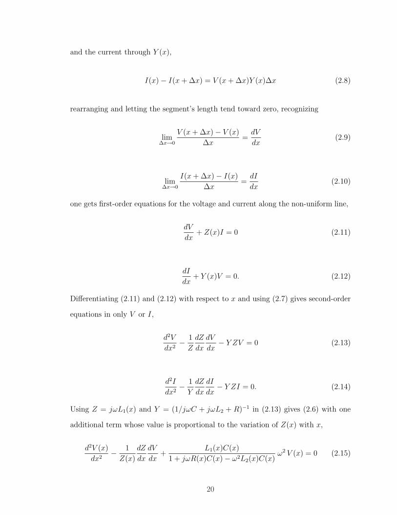
and the current through Y (x),
I(x)− I(x + ∆x) = V (x + ∆x)Y (x)∆x (2.8)
rearranging and letting the segment’s length tend toward zero, recognizing
lim∆x→0
V (x + ∆x)− V (x)
∆x=
dV
dx(2.9)
lim∆x→0
I(x + ∆x)− I(x)
∆x=
dI
dx(2.10)
one gets first-order equations for the voltage and current along the non-uniform line,
dV
dx+ Z(x)I = 0 (2.11)
dI
dx+ Y (x)V = 0. (2.12)
Differentiating (2.11) and (2.12) with respect to x and using (2.7) gives second-order
equations in only V or I,
d2V
dx2− 1
Z
dZ
dx
dV
dx− Y ZV = 0 (2.13)
d2I
dx2− 1
Y
dZ
dx
dI
dx− Y ZI = 0. (2.14)
Using Z = jωL1(x) and Y = (1/jωC + jωL2 + R)−1 in (2.13) gives (2.6) with one
additional term whose value is proportional to the variation of Z(x) with x,
d2V (x)
dx2− 1
Z(x)
dZ
dx
dV
dx+
L1(x)C(x)
1 + jωR(x)C(x)− ω2L2(x)C(x)ω2 V (x) = 0 (2.15)
20

where,
1
Z(x)
dZ
dx=
1
jωL1(x)
d
dx[jωL1(x)] . (2.16)
For long discretized transmission lines (and channelizers with many channels) whose
sections are exponentially-scaled with length (2.16) tends to be very small (i.e. L1
changes very slowly with x), though it must be included in (2.15) if one is interested
in calculating exact solutions of the non-uniform line [52].
21

Chapter 3
Single-order RF Cochlear Channelizers
This chapter applies the previously developed transmission line cochlear model
to the design of two cochlear channelizing filters covering the 20 to 90 MHz band
in 20 contiguous channels. Theory, a design procedure, and results are including for
both fractional and constant bandwidth channelizers. In addition, the time-domain
behavior of these channelizers is examined.
Applications of these channelizing filters include wideband, contiguous-channel
receivers for signal intelligence or spectral analysis. In its simplest form, the channel-
izing filter is used to decompose a wideband input signal into contiguous channels,
whose outputs are then fed to separate amplifiers, mixers, and detectors, providing
simultaneous reception over the entire input bandwidth. By using a less complex re-
ceiver chain (for instance, an envelope detector) at each filter output, this wideband
receiver becomes a spectrum analyzer.
3.1 Channelizer Circuit Design
To arrive at an actual channelizer design, we must choose the element values for
the cochlea-like circuit described by (2.6). For this, we rely on earlier modeling efforts
for the case of a channelizer whose channels have a constant fractional bandwidth.
An alteration of this model allows the design of constant absolute bandwidth filters
described later.
22

3.1.1 Constant Fractional Bandwidth Formulation
In a constant fractional bandwidth channelizing filter, each filter section has the
property,
∆f
f0
≡ 1
Q= constant (3.1)
where f0 and ∆f are the center frequency and bandwidth of a particular channel,
and Q is approximately the loaded quality factor of the series resonant circuit channel
filter; the channel filter’s actual Q is slightly lower due to the loading of adjacent chan-
nels. The channel bandwidth definition used in this design is the difference in (upper
and lower) passband frequencies where adjacent channel transmission responses cross
each other. For a channelizer with constant fractional bandwidth channels, the func-
tional dependence between the coefficients in (2.3) and (2.6) is given by [53] and [54].
Written in terms of the channelizer circuit elements these relations are:
L2(x)C(x) = A1eαx (3.2)
R(x)C(x) = A2e0.5αx (3.3)
L1(x)C(x) = A3eαx. (3.4)
Note that (3.2)–(3.4) define an exponential scaling of resonator component values
required to implement series resonator channels with a constant fractional bandwidth.
In these functions, A1, A2, A3, and α are constants to be determined, while L1, L2, C,
and R are the desired channelizer circuit elements. Using (3.2), the series resonator
branches have a resonant frequency given by,
f0 =1
2π√
L2(x)C(x)=
1
2π√
A1eαx(3.5)
so that their resonant frequencies decrease exponentially as we go from left (input) to
right along the channelizer circuit. Also, note that the loaded Q of each series LCR
23

resonator can be written
Q =X
R=
2πf0L2
R=
1
R(x)
√L2(x)
C(x)(3.6)
so that by using (3.2) and (3.3) in (3.6), we find that the each resonator has an
identical loaded Q, where
Q =
√A1
A2
. (3.7)
Since the fractional bandwidth of each resonator is just the reciprocal of the loaded
Q, the functional dependence of (3.2)–(3.4) results in a channelizer whose channels
exhibit a constant fractional bandwidth.
The number of channels N needed can be estimated as a function of the de-
sired total bandwidth with a given channel fractional bandwidth. First, consider two
adjacent channels, each crossing over at 2 dB below below each channel’s identical
maximum transmission value. The two channels’ center frequencies are related by
fn+1 = fn +∆fn+1
2+
∆fn
2, 1 ≤ n ≤ N. (3.8)
Using (3.1) to write ∆f in terms of fractional bandwidth (1/Q), this becomes
fn+1
fn
=1 + 1/2Q
1− 1/2Q. (3.9)
For an N channel channelizer the maximum and minimum frequencies are related
by
fmax
fmin
=fN
f1
=
(1 + 1/2Q
1− 1/2Q
)N−1
(3.10)
and,
N = 1 +
ln
(fN
f1
)
ln
(1 + 1/2Q
1− 1/2Q
) . (3.11)
24

Note that since the series resonator channel filters are coupled to and loaded by
adjacent resonators, each channel filter’s loaded Q is less than that of the isolated
series resonator. Consequently, one needs to use a slightly larger value of Q in the
design process to produce the desired fractional bandwidth channels. For example, as
illustrated later, channels with 8.2% fractional bandwidth (Q = 12.2) use resonators
with a Q of 15.6 (28% higher). One uses the actual channel filter Q in (3.11).
3.1.2 Determination of Coefficients
The coefficients A1, A2, A3, and α are determined by four design choices, including:
f1 ≡ Lowest channel center frequency
fN ≡ Highest channel center frequency
1/Q ≡ Channel fractional bandwidth
θ ≡ Transmisson phase at each channel’s center frequency
The choice of θ is arbitrary, and its value affects the input impedance and overall
channelizer response. The design must therefore be simulated with various θ val-
ues until the desired response is achieved. Interestingly, the channelizer exhibits a
characteristic S11 spiral which moves along the real axis of the Smith Chart as one
varies θ from zero to values approaching roughly 2π (Fig. 3.1). The channelizer mini-
mum and maximum channel center frequencies and channel fractional bandwidth are
chosen based on the application.
The resonator nearest the channelizer input (x = 0) is tuned at the highest fre-
quency (fN). Using (3.2) with x = 0, and (3.5), A1 is given by
A1 =1
(2πfN)2 . (3.12)
25

(c)
θ = 1.6π
(b)
θ = 0.9π
(a)
θ = 0.5π
Figure 3.1: Channelizer S11 for three values of θ. A θ value of 0.9π (b) produces aninput return loss of less than −10 dB over the band from 20–90 MHz.The Smith Chart impedance is 50 Ω.
Next, to determine A2, one uses the desired channel fractional bandwidth and (3.6)
to arrive at
A2 =
√A1
Q. (3.13)
To find α, (3.2) and (3.12) are used at the channelizer input (x = 0) and final
section (x = 1) where
x = 1 ⇒ A1eα =
1
(2πf1)2
x = 0 ⇒ A1 =1
(2πfN)2
such that
α = ln
(fN
f1
)2
. (3.14)
Finally, A3 is found using a numerical technique and the previously determined
constants. The Wentzel-Kramers-Brillouin (W.K.B.) approximation suggests that if
g(x) changes slowly enough with x, then we can approximate the solution to
d2
dx2u(x) + g(x) · u(x) = 0 (3.15)
26

at some x = x0 by the solution
u(x0) = U0ej∫ x00
√g(x)dx = U0e
jθ. (3.16)
Comparing (3.15) with (2.6), we let
g(x) =L1(x)C(x)
1 + jωR(x)C(x)− ω2L2(x)C(x)ω2
and
u(x) = V (x).
Thus, we can find the phase of (3.16) using
θ ≈x0∫
0
√g(x) dx. (3.17)
In (3.17), θ is the phase of u(x) at location x0 which is the location of a resonator
with a center frequency f0. The transmission phase at the center frequency of each
resonator θ is assumed to be constant in analogy with physiological cochlear response
data [55, 56].
Having found A1, A2, and α, and choosing a value of θ, (3.17) is numerically
integrated along the channelizer length (x) for each value of x0. For each point x0
along x an integral is evaluated and the needed term L1(x)C(x) is found. The result
is an arbitrary function which is then fit to the desired form of (3.4), giving the value
of A3.
Having found the four constants A1, A2, A3, and α, each circuit component of
the constant fractional bandwidth channelizer is determined from (3.2)–(3.4). In our
designs, the value of R(x) is made constant for each resonator section to ensure a
constant impedance at each output port. Therefore, first C(x) is determined from
27

(3.3), then L1(x) and L2(x) are calculated from (3.4) and (3.2).
3.1.3 Constant Absolute Bandwidth Formulation
In many cases, a channelizer filter with a constant absolute bandwidth (∆f) out-
puts is needed. In this case, the number of channels needed to cover a specified
bandwidth is given by
N = 1 +fN − f1
∆f. (3.18)
Such a channelizer results from modifying the functional dependence of the channel
center frequencies from exponential to linear.
For a constant channel bandwidth, the channel center frequencies are given by
f0 = B1 + B2x. (3.19)
Equating this with the resonant frequency of a series LCR resonator results in
L2(x)C(x) =1
[2π (B1 + B2x)]2. (3.20)
Using (3.19) and (3.20) in (3.6), we obtain
R(x)C(x) =∆f
2π (B1 + B2x)2 . (3.21)
Combining (3.20) and (3.21) leads to,
L2(x) =R(x)
2π∆f(3.22)
and for resonators with identical output impedance (R(x)), the resonator inductance
value (L2(x)) is also fixed and inversely proportional to the channel bandwidth. Note
that this relationship places a practical restriction on the realizable bandwidth of the
28

constant absolute bandwidth design, for a given channel bandwidth, due to inductor
parasitics: the channelizer’s maximum frequency must be below the inductor’s self-
resonant frequency.
Suggested by the form of (3.21), the last relationship among the circuit elements
is chosen as
L1(x)C(x) =1
[2π (B3 + B4x)]2. (3.23)
This was found empirically to result in a channelizer with constant absolute band-
width channels as well as a good input impedance match over the entire channelizer
bandwidth.
3.1.4 Determination of Coefficients
For the channelizer with constant absolute bandwidth channels, the coefficients
B1, B2, B3, and B4 are determined from the chosen values of:
f1 ≡ Lowest channel center frequency
fN ≡ Highest channel center frequency
∆f ≡ Channel absolute bandwidth
θ ≡ Transmission phase at each channel’s center frequency
Since the highest frequency resonator appears at the channelizer input (x = 0), using
(3.19) we find that,
B1 = fN . (3.24)
At the lowest frequency resonator (x = 1), again using (3.19), we find that
B2 = f1 − fN . (3.25)
29
Finally, the constants B3 and B4 are determined by using the same numerical
integration and curve fitting procedure used in the constant fractional bandwidth
design. However, in the constant absolute bandwidth case (3.23) is substituted in the
kernel g(x) of (3.17). Again here, the choice of the phase at each center channel (θ)
is adjusted by trial-and-error in simulation to optimize channelizer input return loss.
Having found B1, B2, B3, and B4, the channelizer circuit elements are determined.
With R(x) constant, L2(x) is given by (3.22), C(x) is found using (3.20), and L1(x)
is given by (3.23).
3.2 Experimental Results
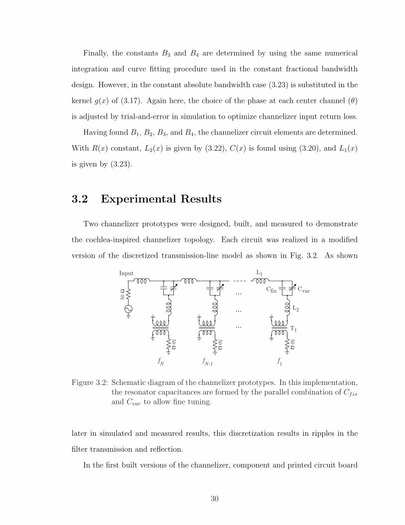
Two channelizer prototypes were designed, built, and measured to demonstrate
the cochlea-inspired channelizer topology. Each circuit was realized in a modified
version of the discretized transmission-line model as shown in Fig. 3.2. As shown
50 Ω
50 Ω
fN-1
fN
L1
f1
T1
L2
CvarCfix
50 Ω
50 Ω
Input
Figure 3.2: Schematic diagram of the channelizer prototypes. In this implementation,the resonator capacitances are formed by the parallel combination of Cfix
and Cvar to allow fine tuning.
later in simulated and measured results, this discretization results in ripples in the
filter transmission and reflection.
In the first built versions of the channelizer, component and printed circuit board
30

(PCB) parasitics caused unwanted in-band resonances, emphasizing the need for ac-
curate simulation. For the prototypes presented here, circuit simulations were per-
formed in Agilent ADS [57] using manufacturer provided S-parameters of all lumped
components except for the RF transformers. The RF transformer S-parameter blocks
were generated from a de-embedded fixture measurement. Board parasitics were ac-
counted for using an S-parameter block derived from a full-wave Sonnet model [58].
The resulting simulations accurately predicted parasitic resonances.
3.2.1 Constant Fractional Bandwidth Channelizer
A 20-channel channelizer with constant fractional bandwidth channels covering
20–90 MHz is shown in Fig. 3.3. The series inductances L1 are air-wound inductors
Figure 3.3: Photograph of the 20-channel, 20–90 MHz channelizing filter with con-stant fractional bandwidth channels. The inset shows a single channellayout.
(Coilcraft Midi Spring) with Q of 60–100 over the channelizer bandwidth. The shunt
31
resonator sections are designed for a loaded Q of 16 and |XL|=|XC |=200 Ω at res-
onance, resulting in an effective impedance of 12.5 Ω. This is transformed to 50 Ω
through a 1:2 turns ratio RF transformer (Coilcraft TTWB) at each channel output.
The shunt resonator inductors L2 (Coilcraft 0805CS) are ceramic body wire-wound
surface-mount components with Q of 25–40 at the channel center frequencies. To
take into account the tolerance in the component values and since the capacitors and
inductors are commercially available in discrete values, the resonator capacitances
C are implemented with the parallel combination of a fixed surface-mount capacitor
(ATC 600F) and a coaxial trimmer capacitor (Sprague GAA). The trimmer capacitor
was included to ease the tolerance requirement of the other components—a design
using all fixed-value components (±2%) is certainly possible. The total capacitor Q
is greater than 200 over the channelizer bandwidth. Channelizer component design
values range from 30 nH to 37 nH for L1, 310 nH to 1570 nH for L2, and 8 pF to
40 pF for C (Fig. 3.4). The circuit is constructed on a 61 mil FR-4 PCB (Fig. 3.3)
with the ground located along the perimeter of the PCB to reduce shunt parasitic
capacitance. Simulations on two-sided PCB identified significant layout parasitics
that gave undesirable spurious responses within the filter pass-band.
3.2.2 Measurements
The channelizer is tuned by adjusting the trimmer capacitors on individual channel
resonators until nulls in the measured S11 match the simulated response (Fig. 3.5).
The tuning procedure involved first setting each trimmer at maximum capacitance,
then adjusting for the desired response by lowering the appropriate trimmer value
beginning with the highest frequency channel. Channelizer measured and simulated
S21 for each channel (S(n+1)1 for 1 ≤ n ≤ 20) are shown in Fig. 3.6. Measured
insertion loss at the center of each channel ranges from 2.5 dB to 5.3 dB, with an
average of 4.8 dB.
32

L2 (
nH
)
0
200
400
600
800
1000
1200
1400
1600
C (
pF
)
10
20
30
40
Channel Number
10 12 14 16 18 20
L1 (
nH
)
28
30
32
34
36
38
8642
Figure 3.4: Component values for L1, L2, and C for the 20–90 MHz constant frac-tional bandwidth (8%) channelizer.
A sample of three separate channel responses is shown in Fig. 3.7. Focusing on
channel 10, we notice the characteristic cochlear response. The pass-band slope is
first-order (20 dB/decade) below the channel center frequency and over fifth-order
(100 dB/decade) immediately above the channel center frequency due to the low-
pass nature of the dispersive transmission-line. Note that for frequencies outside of
the channelizer bandwidth, each channel has a characteristic single LCR response.
This can be seen as an increase in S21 for all channels beginning at both 20 MHz
and 90 MHz. Also, the self-resonance of the resonator inductors produces a parasitic
resonance at 150 MHz. The measured center frequencies and channel responses match
simulation closely. Adjacent channel S21 cross at approximately 2 dB below each
channel’s center frequency (Table 3.1). Each channel’s 2-dB crossover bandwidth is
8.2±0.1%. Spurious responses above 100 MHz are due to resonances of the lumped
33

Frequency (MHz)
S11
(d
B)
-25
-20
-15
-10
-5
0
10 100 20020 50
Figure 3.5: Measured (solid) and simulated (dashed) S11 of the 20-channel constantfractional bandwidth channelizer.
inductors as well as PCB parasitic shunt capacitance.
Table 3.1: Channelizer Center Frequencies (in MHz)
Ch fc Ch fc Ch fc Ch fc
1 19.2 6 28.7 11 42.4 16 62.4
2 20.8 7 31.1 12 46.0 17 67.3
3 22.5 8 33.5 13 49.6 18 72.6
4 24.4 9 36.3 14 53.8 19 78.2
5 26.5 10 39.4 15 58.0 20 84.3
To understand the channelizer loss, consider the power distribution at the center
frequency of channel 10 (39.4 MHz) (Table 3.2). The percent of the input power
appearing at the individual outputs is calculated from each channel’s measured |S21|2.Likewise, the reflected power at the channelizer input is given by |S11|2. At 39.4 MHz,
33.2% of the power arrives at the channel 10 output (−4.8 dB), 32.3% appears at
all other channel outputs (Fig. 3.8), and 3.5% is reflected at the channelizer input.
Summing the powers results in 69.0% of the input power. Thus, the filter dissipates
34

Frequency (MHz)
S21
(d
B)
-60
-50
-40
-30
-20
-10
0
10 100 20020 50
Frequency (MHz)
10 100
S21
(d
B)
-60
-50
-40
-30
-20
-10
0
20020 50
Figure 3.6: Simulated (top) and measured (bottom) S21 for each channel of the chan-nelizing filter.
31.0% of the input power corresponding to an effective loss of 1.6 dB.
3.2.3 Constant Absolute Bandwidth Channelizer
The 20-channel channelizer with constant absolute bandwidth channels covering
roughly 20–90 MHz is shown in Fig. 3.9. This design also uses high-Q surface-mount
35

Frequency (MHz)
10 100
S21
(dB
)
-60
-50
-40
-30
-20
-10
0
20 50 200
Ch. 3 Ch. 10 Ch. 17
Figure 3.7: Measured (solid) and simulated (dashed) S21 of the constant fractionalbandwidth channelizer for channels 3 (22.5 MHz), 10 (39.4 MHz), and 17(67.3 MHz). Ripples are due to parasitics and resonances of the lumpedcomponents.
Channel Number
2 4 6 8 10 12 14 16 18 20
|S21|2
0.0
0.1
0.2
0.3
0.4
Figure 3.8: Measured power distribution at the center frequency of channel 10 (39.4MHz) among all 20 channels.
components throughout, with air-coil inductors for both L1 and L2 (Coilcraft Midi
and Maxi Spring). In contrast to the constant fractional bandwidth case, the individ-
ual channel resonators have a loaded Q that varies with resonator center frequency,
producing constant absolute channel bandwidth. The resonators are again designed
36

Table 3.2: Sample Channel Power Distribution for Channel 10
Power (%)
Channel 10 Output 33.2 (−4.8 dB)
Sum of Channel 1–9, 11–20 Outputs 32.3
Reflected at Input 3.5
Sum of all Power Contributions 69.0
Power Dissipated 31.0
L1
L2
Cvar
Cfix
T1
3.3 in
1.1 in
Ground
Figure 3.9: Photograph of the 20-channel, 20–90 MHz channelizing filter with con-stant absolute bandwidth channels. The inset shows a single channellayout.
for a series resistance, at resonance, of 12.5 Ω and 1:2 turns ratio RF transform-
ers (Coilcraft WB1040) are used at each channel output to produce a 50 Ω output
impedance. The resonator capacitances C also employ a parallel combination of a
fixed capacitor (ATC 600F) and a coaxial trimmer capacitor (Sprague GAA) to al-
low for fine-tuning channel center frequencies. Channelizer component design values
37

range from 19 nH to 296 nH for L1 and 5 pF to 150 pF for C, while L2 is fixed at
422 nH (Fig. 3.10).
L2 (
nH
)
200
400
600
800
1000
1200
1400
1600
C (
pF
)
0
50
100
150
Channel Number
2 4 6 8 10 12 14 16 18 20
L1 (
nH
)
0
100
200
300
Figure 3.10: Component values for L1, L2, and C for the 20–90 MHz constant absolutebandwidth channelizer.
3.2.4 Measurements
The channelizer is tuned by adjusting the trimmer capacitors on individual channel
resonators until nulls in the measured S11 match the simulated response (Fig. 3.11)
assuring the correct resonator center frequencies. Measured and simulated S21 for
each channel (S(n+1)1 for 1 ≤ n ≤ 20) are shown in Fig. 3.12 while a sample of
three separate measured channel responses is shown in Fig. 3.13 showing good agree-
ment with simulations. Measured insertion loss at the center of each channel ranges
from 1.9 dB to 4.8 dB, with an average of 4.3 dB. The measured center frequencies
38

Frequency (MHz)
20 40 60 80 100
S11
(dB
)
-25
-20
-15
-10
-5
0
Figure 3.11: Measured (solid) and simulated (dashed) S11 of the 20-channel constantabsolute bandwidth channelizer.
and channel responses again match simulation closely. As in the constant fractional
bandwidth case, adjacent channel S21 responses cross at ∼ 2 dB below each channel’s
center frequency (Table 3.3). Each channel’s 2-dB crossover bandwidth is a nearly-
constant 4 MHz, resulting in fractional bandwidths ranging from 26.0% (channel 1)
to 4.3% (channel 20).
Table 3.3: Channelizer Center Frequencies (in MHz)
Ch fc Ch fc Ch fc Ch fc
1 15.4 6 37.8 11 58.5 16 78.6
2 20.5 7 42.4 12 62.5 17 82.6
3 25.1 8 46.4 13 66.5 18 86.7
4 29.2 9 50.4 14 70.6 19 90.1
5 33.8 10 54.5 15 74.6 20 93.6
The power distribution at the center frequency of channel 10 (54.5 MHz) is shown
in Table 3.4. The percent of the input power appearing at the individual outputs
39

Frequency (MHz)
20 40 60 80 100
S2
1 (
dB
)
-60
-50
-40
-30
-20
-10
0
Frequency (MHz)
20 40 60 80 100
S2
1 (
dB
)
-60
-50
-40
-30
-20
-10
0
Figure 3.12: Simulated (top) and measured (bottom) S21 for each channel of theconstant absolute bandwidth channelizing filter. The frequency scale islinear to show the constant absolute bandwidth response.
is calculated from each channel’s measured |S21|2 and the reflected power at the
channelizer input is given by |S11|2. At 54.5 MHz, 35.4% of the power arrives at the
channel 10 output (−4.5 dB), 39.8% appears at all other channel outputs (Fig. 3.14),
and 5.8% is reflected at the channelizer input. Summing the powers results in 81.0%
of the input power. Thus, the filter dissipates 19.0% of the input power corresponding
40

Frequency (MHz)
20 40 60 80 100
S2
1 (
dB
)
-60
-50
-40
-30
-20
-10
0Ch. 3 Ch. 10 Ch. 17
Figure 3.13: Measured (solid) and simulated (dashed) S21 of the constant absolutebandwidth channelizer for channels 3 (25.1 MHz), 10 (54.5 MHz), and17 (82.6 MHz).
to an effective loss of 0.9 dB.
Channel Number
2 4 6 8 10 12 14 16 18 20
|S21|2
0.0
0.1
0.2
0.3
0.4
Figure 3.14: Measured power distribution at the center of channel 10 (54.5 MHz)among all 20 channels.
41

Table 3.4: Sample Channel Power Distribution for Channel 10
Power (%)
Channel 10 Output 35.4 (−4.5 dB)
Sum of Channel 1–9, 11–20 Outputs 39.8
Reflected at Input 5.8
Sum of all Power Contributions 81.0
Power Dissipated 19.0
3.3 Channel Filter Properties
3.3.1 Channel Phase Response
From the results presented so far, we see that a channelizing filter based on cochlear
modeling produces channels with near-uniform amplitude response; a characteristic
|S21| scaled in frequency from one channel to the next. In addition, from data on
biological cochlea measurements, we expect that the phase of S21 at each center
frequency is nearly identical for all channels [55, 56]. This is shown in measured and
simulated results for the RF channelizers (Fig. 3.15).
The uniformity among channel response in amplitude, phase, and phase constancy
at the center frequency is determined by the number of sections physically preceding
a particular channel. Typically a minimum of five sections are needed to set up the
characteristic response. Since these initial sections are the higher frequency channels,
the lower frequency sections of the channelizer have the most uniform response.
3.3.2 Transient Response
In many situations it is desirable to decompose a wideband input signal into
narrower channels in real time. Transient simulations were done to demonstrate this
channelizing filter’s capability in such a system. These simulations were performed
42

Channel Number
2 4 6 8 10 12 14 16 18 20
-180
-160
-140
-120
-100
-80
-60
-40
-20
0
20
40
Simulation
Measurement
S2
1 P
has
e (D
egre
es)
Channel Number
2 4 6 8 10 12 14 16 18 20
-160
-140
-120
-100
-80
-60
-40
-20
0
20
40
Simulation
Measurement
S2
1 P
has
e (D
egre
es)
Figure 3.15: Measured and simulated phase of S21, at each channel’s center frequency,for the constant fractional bandwidth version (top) and the constantabsolute bandwidth version (bottom). The data for each channel istaken at the center frequency of the particular channel.
using the constant absolute bandwidth channelizer. Finite Q, but otherwise ideal,
lumped elements were used to reduce transient simulation complexity. Because the
simulation did not include component or board parasitics, the channel responses were
shifted slightly up in frequency compared with the previous S-parameter simulations.
A Gaussian monopulse filtered through a high-order maximally flat filter was
43
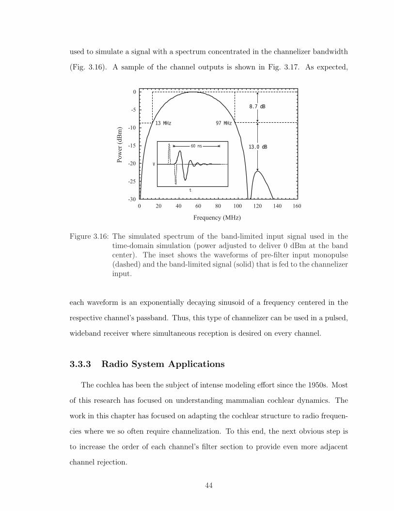
used to simulate a signal with a spectrum concentrated in the channelizer bandwidth
(Fig. 3.16). A sample of the channel outputs is shown in Fig. 3.17. As expected,
Frequency (MHz)
Pow
er (
dB
m)
-30
-25
-20
-15
-10
-5
0
100 120 140 160806040200
97 MHz13 MHz
13.0 dB
8.7 dB
t
V
60 ns
Figure 3.16: The simulated spectrum of the band-limited input signal used in thetime-domain simulation (power adjusted to deliver 0 dBm at the bandcenter). The inset shows the waveforms of pre-filter input monopulse(dashed) and the band-limited signal (solid) that is fed to the channelizerinput.
each waveform is an exponentially decaying sinusoid of a frequency centered in the
respective channel’s passband. Thus, this type of channelizer can be used in a pulsed,
wideband receiver where simultaneous reception is desired on every channel.
3.3.3 Radio System Applications
The cochlea has been the subject of intense modeling effort since the 1950s. Most
of this research has focused on understanding mammalian cochlear dynamics. The
work in this chapter has focused on adapting the cochlear structure to radio frequen-
cies where we so often require channelization. To this end, the next obvious step is
to increase the order of each channel’s filter section to provide even more adjacent
channel rejection.
44

-1
0
1
T3
1f3
28.2 MHz= =T3
Vo
ltag
e (V
)-1
0
1
T10 T
10
1f10
59.0 MHz= =
Time (nsec)
0 100 200 300
-1
0
1
T17
T17
1f17
84.3 MHz= =
Figure 3.17: Three representative simulated waveforms that appear at channelizeroutput ports with the input signal shown in Fig. 3.16.
In theory, the cochlea-inspired channelizer topology can be applied to any fre-
quency range. One obvious limitation is the effect of lumped component (especially
inductor) self-resonances which produce undesirable responses within the total chan-
nelizer bandwidth. For channelizers covering many octaves, one must also mitigate
the harmonic responses of distributed filter sections.
The cochlea-inspired channelizer circuit is a wide bandwidth contiguous channel
multiplexer with a large number of channels. Conventional manifold type RF and
microwave multiplexers using high-Q resonator technologies can achieve lower inser-
tion loss and arbitrary pass-band responses, but with a limited number of channels
(due to design complexity). Such high performance filters also come with a high cost
and large size. In applications such as receiver front-end preselection and instanta-
neous spectrum monitoring, where lower stop-band rejection can be traded for a large
number of channels, a cochlea-like channelizer fulfills the need with a straightforward
design method.
45

Chapter 4
Microwave Planar Cochlear Channelizers
Channelization is also useful in higher frequency applications, such as ultra-
wideband (UWB) systems. Often, only part of the spectrum is used at a time. In cases
where strong adjacent channel interference exists, one can channelize the wideband
input signal into narrow sub-bands which are then applied to active receiver stages
(amplifiers, mixers, analog-to-digital converters). By virtue of its increased adjacent-
channel rejection, such a preselection scheme increases receiver dynamic range and
reduces intermodulation products. Alternatively, the same kind of preselector can
be used to feed simple diode detectors resulting in a wideband instantaneous spec-
trum activity monitor (Fig. 4.1), which is important for UWB and/or cognitive radio
systems.
Preselector
RX Ch N
RX Ch 1
f1fN
Figure 4.1: A spectrum activity monitoring receiver using a channelizing preselectorfilter.
In this chapter, a compact microwave channelizing preselector filter is presented
covering 2–7 GHz in 15 channels suited for integration in UWB receiving systems.
The filter is completely passive, and thus features high linearity and zero d-c power
46

consumption. In addition, an overview of component modeling used in the channelizer
design is included.
4.1 Theory
The channelizer’s structure is directly related to a 1-dimensional cochlear model
whose lumped-element prototype schematic is shown in Fig. 4.2a [59]. Such a channel-
f1
R1
∆x
L21
∆x
C ∆x
L1 ∆x V(x)
Wideband
Input
x
fN-1
fN
(Outputs)
RLoad
(highest freq.) (lowest freq.)
50
Ω
50
Ω
L1
C2
L2
CtrimC1
50 Ω
50
Ω
Input
Output 1Output N Output N-1
(a)
(b)
Figure 4.2: (a) Discretized, non-uniform transmission-line model of the basilar mem-brane (located within the cochlea). The channelizer is synthesized fromthis model. (b) Integrated channelizing filter schematic diagram. Trim-mer capacitors are used to fine tune resonator center frequencies andan L-C matching network transforms the resonator output impedance to50 Ω.
izer uses a cascade of shunt-connected series resonators coupled by series inductances.
The series resonators form the individual channel filters whose upper stop-band re-
sponse is enhanced by the presence of all higher frequency sections. The resulting
47

circuit offers a compact way of channelizing a wide bandwidth into many channels
with a straightforward design method.
The silicon-based channelizer uses high-Q integrated lumped-element components
to cover the 2–7 GHz band. The implemented circuit schematic is shown in Fig. 4.2b.
The inclusion of an output L-C matching network at each resonator transforms the
resonator’s equivalent resistance at resonance (RLoad = 6.25 Ω in this design) to a
50 Ω output port. The L-C network works well in each resonator’s passband and
offers additional stop-band rejection for out-of-band signals. In the actual layout, the
matching network’s inductor is absorbed within L2, and the shunt capacitor C2 is
placed at each resonator’s output terminal.
4.2 Circuit Design
The lumped element values, L1, L2, C, and R, for the channelizer circuit (Fig. 4.2a)
are found from the functional dependence described in [59]. In this model four con-
stants, α, A1, A2, and A3 determine the LCR components of the channelizer by:
L2(x)C(x) = A1eαx (4.1)
R(x)C(x) = A2e0.5αx (4.2)
L1(x)C(x) = A3eαx (4.3)
where x is the normalized transmission line length with x = 0 corresponding to the
channelizer input. These constants are found with the specification of four design
choices: minimum channel frequency f1, maximum channel frequency fN , number of
channels N , and the transmission phase θ at each channel’s center frequency (referred
to the channelizer input). The parameter θ is assumed constant at the center of each
channel based on measured acoustic cochlear data [55, 56], and primarily influences
48

the network’s input impedance through the specification of the coupling inductances
L1.
The channelizer presented here is designed to cover 2 to 7 GHz in 15 channels
(16% bandwidth) with an input impedance of 50 Ω. The required lumped-element
values range from 2.10 nH to 7.60 nH for L2, 220 fF to 1.25 pF for C1, and 1.20 pF
to 4.80 pF for C2. In the prototype circuit covering several decades, L1 increases
exponentially with position along the channelizer. In designs covering less than two
octaves, the variation is small enough that approximating L1 with a single value works
well. In this design, L1 is a constant 0.7 nH inductor.
4.3 Layout and Fabrication
The lumped-element realization of this circuit is done using the M.I.T. Lincoln
Laboratory Precision Multi-Chip Module (P-MCM) process. This technology offers
high-Q suspended inductors and metal-insulator-metal (MIM) capacitors, along with
three metal signal layers, a tantalum resistor layer, tungsten vias, and a 20 µm thick
gold top metal layer (Fig. 4.3) [60].
The resonator inductors L2 primarily determine the unloaded Q of the filter sec-
tions and thus the channel filter insertion loss. L2 is implemented using suspended
spiral inductors which have measured unloaded Qs of 35–45 from 2–7 GHz, for values
of 2.10 nH to 7.60 nH, all using 20 µm wide lines and 20 µm spacing. The coupling
inductors L1 are standard spirals (not suspended), also use 20 µm width and spacing,
and have Qs ranging from 25–30 from 2–7 GHz.
Two types of MIM capacitors are used. The resonator capacitors (C1) are com-
posed of signal 1 and signal 2 metal layers separated by 7.315 µm of SiO2 (Fig. 4.3).
This was chosen to result in reasonable dimensions for C1 (0.22 pF to 1.25 pF). To
facilitate post-fabrication resonator fine tuning, the top plates incorporate adjacent
49

TOP METAL
GROUND PLANE
SIGNAL 2
SIGNAL 1
SIGNAL 3 SIGNAL 3
SIGNAL 2
POWER PLANE
SIGNAL 3
SIGNAL 1
POWER PLANE
VIA
1
RESISTOR VIA
VIA
2V
IA 3
VIA 4
5µm
5µm
5µm
2µm
2µm
INTEGRALDECOUPLINGCAPACITOR
0.065µm
7µm
7µm
7µm
VIA
3
VIA
3V
IA 2
VIA
2
VIA
1
3 LAYERMEMBRANE FOR
SUSPENDEDSTRUCTURES
Al
Al
Al
Al
Al
SiO2
SiO2
SiO2
SiO2 0.25µm
UNDERBUMP
METAL
OGC
TUNGSTEN VIAS
BACKSIDE TRENCHETCH 675 µm
DRAWING NOT TO SCALE
TOP METAL2µm
20µm
Si
Figure 4.3: The Precision Multi-Chip Module (P-MCM) process developed by M.I.T.Lincoln Laboratory.
smaller plates that can be wire-bonded to increase the total resonator capacitance
by up to 20% (Fig. 4.4). The shunt L-C matching network capacitors C2 (1.2 pF to
C1Ctrim
80 mm
Optional
Wirebond
C1
Ctrim
Figure 4.4: A close-up view of the resonator capacitor. The main top plate can bewire bonded to smaller auxiliary plates to increase capacitance and re-tune the resonator’s center frequency.
4.8 pF) use the power and ground plane metal layers separated by 150 nm of Al2O3,
50

and both types of capacitors have a measured Q greater than 60 at their respective
resonator’s center frequencies.
On-chip resistors are used to terminate channels 1 and 15. This was done to allow
testing of channels 2 through 14 with a 14-port wafer probe; as is well known, each
channel must be terminated in 50 Ω for S-parameter measurements.
Each inductor, capacitor, and interconnect line is modeled with Sonnet software
[58] and the results exported as S-parameters for analysis in Agilent ADS [57]. The
entire circuit is then modeled in ADS.
4.4 Results
A microphotograph of the fabricated channelizer chip is shown in Fig. B.3. The
channelizer input is on the left and the channel resonators extend rightward with
decreasing center frequency. Wire bonds connecting opposite edges of the top-metal
pattern mitigate in-band ground loop resonances. Ground-signal-ground (GSG) probe
pads occupy the die perimeter (not shown) and connect to microstrip lines for the
input and channel output ports.
A set of test structures including individual channel resonator sections is included
on each sample wafer. The transmission response (S21) of each resonator is measured
and compared to simulation. In cases where the measured resonant frequency is
higher than expected, additional top plate area is bonded to the respective resonator
capacitor C1 (Fig. 4.4).
The filter’s S-parameters are measured using an on-wafer probing set-up. A 2-port
short-open-load-thru (SOLT) calibration places the measurement reference planes at
the GSG probe pads. A total of 14 GSG probes are available, allowing the simultane-
ous termination of 13 channel output ports (and one input port). The S-parameters
of channels 2 through 14 are measured individually while all other channels are ter-
51

minated with 50 Ω loads through wafer probes. (Channels 1 and channel 15 are
terminated with integrated resistors on the silicon wafer.)
The measured and simulated input reflection (S11) for the complete channelizer
is shown in Fig. 4.7 and the transmission response (S21) for each channel is shown in
Fig. 4.8 and Fig. 4.9.
Using the trimmer capacitor scheme, channels 2 through 14 are tuned to within
−5.5% and +2.2% of their target center frequencies (most were within ±2%). The
S21 responses of each channel (Figs. 4.8 and 4.9) exhibit the cochlea-like response
seen in previous RF channelizer designs [59] and biological cochlea data. The lower
stop-band exhibits a 20 dB/decade second-order (single resonator) response while
the upper stop-band rolls off at greater than 100 dB/decade. The enhanced response
above the passband is due to additional poles created by higher frequency channels
that appear before a particular channel resonator.
52

Ch
15
Inp
ut
L1
L2
C1+
Ctr
im
50
ΩC
2
Ch
14
Ch
13
Ch
12
Ch
11
Ch
10
Ch
9
Ch
8
Ch
7
Ch
6
Ch
5
Ch
4
Ch
3
Ch
2
Ch
1M
icro
str
ip lin
e (
50 Ω
) to
pro
be p
ads
Fig
ure
4.5:
Am
icro
phot
ogra
ph
ofth
e15
-chan
nel
chan
nel
izer
.T
he
chip
mea
sure
s3.
4m
mby
14.1
mm
,not
incl
udin
gth
em
icro
stri
plines
lead
ing
topro
be
pad
s(n
otsh
own).
Chan
nel
s1
(furt
hes
tfr
omin
put)
and
15(n
eare
stto
input)
are
inte
rnal
lyte
rmin
ated
in50
Ω.
All
other
chan
nel
sar
epro
bed
usi
ng
CP
Wpro
be
pad
s(n
otsh
own).
Dio
de
det
ecto
rsca
nbe
pla
ced
atea
chch
annel
outp
ut
for
spec
trum
acti
vity
mon
itor
ing.
53

Figure 4.6: On-wafer S-parameter measurement set-up at M.I.T. Lincoln Labora-tory. A channelizer under test is in the center of the wafer chuck. Fourmulti-port RF probes (total of 14 ports) allow a single two-port channelmeasurement while simultaneously terminated 13 other channels.
54
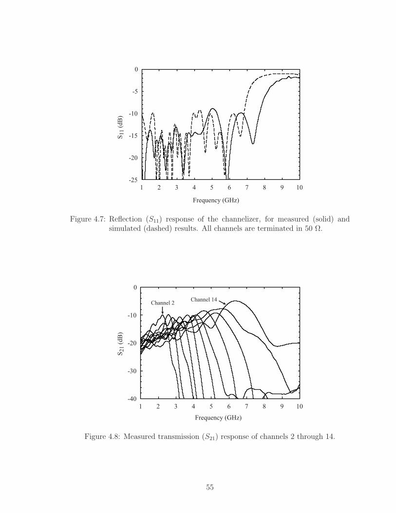
Frequency (GHz)
1 2 3 4 5 6 7 8 9 10
S11 (
dB
)
-25
-20
-15
-10
-5
0
Figure 4.7: Reflection (S11) response of the channelizer, for measured (solid) andsimulated (dashed) results. All channels are terminated in 50 Ω.
Frequency (GHz)
1 2 3 4 5 6 7 8 9 10
S2
1 (
dB
)
-40
-30
-20
-10
0
Channel 2Channel 14
Figure 4.8: Measured transmission (S21) response of channels 2 through 14.
55
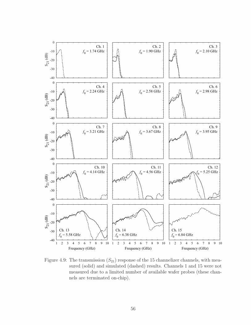
S21
(dB
)
-40
-30
-20
-10
0
S21
(dB
)
-40
-30
-20
-10
0
Frequency (GHz)
21 3 4 5 6 7 8 9 10
Frequency (GHz)
21 3 4 5 6 7 8 9 10
Frequency (GHz)
21 3 4 5 6 7 8 9 10
S21
(dB
)
-40
-30
-20
-10
0
S21
(dB
)
-40
-30
-20
-10
0
S21
(dB
)
-40
-30
-20
-10
0
Ch. 1
f0 = 1.74 GHz
Ch. 2
f0 = 1.90 GHz
Ch. 3
f0 = 2.10 GHz
Ch. 4
f0 = 2.24 GHz
Ch. 5
f0 = 2.58 GHz
Ch. 6
f0 = 2.98 GHz
Ch. 7
f0 = 3.21 GHz
Ch. 8
f0 = 3.67 GHz
Ch. 9
f0 = 3.95 GHz
Ch. 10
f0 = 4.14 GHz
Ch. 11
f0 = 4.56 GHz
Ch. 12
f0 = 5.25 GHz
Ch. 13
f0 = 5.58 GHz
Ch. 14
f0 = 6.38 GHz
Ch. 15
f0 = 6.84 GHz
Figure 4.9: The transmission (S21) response of the 15 channelizer channels, with mea-sured (solid) and simulated (dashed) results. Channels 1 and 15 were notmeasured due to a limited number of available wafer probes (these chan-nels are terminated on-chip).
56

The insertion loss of each channel ranges from 4.9 dB to 14.3 dB with most
channels having an insertion loss of ∼ 9 dB, where 1 dB is due to the microstrip
line length and coplanar waveguide (CPW) probe transition. The remaining loss
is dominated by resonator inductor and capacitor conductor losses (the resonators
have unloaded Qs of 25–30) and conductor and radiation loss of the high-impedance
interconnect line which connects the channels. Modeling shows that the average
insertion loss can be improved to 5 dB by modifying the interconnect line and shielding
the circuit.
4.5 P-MCM Component Modeling
Success of the previously described channelizer depended on accurate modeling of
the lumped-element components implemented in the P-MCM process. No scalable in-
ductor, capacitor, or resistor models existed for this non-commercial process, though
a good amount of measured data was available to compare with existing, general mod-
els and equations. The channelizer circuit was first designed with ideal components.
The design process proceeded by using approximate formulas for lumped-elements
[61] and then simulating each component in a moment-method simulator [58] using
the technology stack-up shown in Fig. 4.3. Test structures, breaking out the each
inductor and capacitor value used, were also fabricated in order to validate the mod-
eling work. The full-wave models were simplified in some cases to lessen computer
memory requirements. In particular, the suspended inductors were simulated with
an air layer below the inductor, instead of a circular air cavity surrounded by silicon
(Fig. 4.10). The simulation reference planes were placed immediately after the probe
pad layout. The pads were de-embedded from the measured data by introducing
−27 pF capacitors at each port.
A comparison of measured and simulated inductance values for all inductors is
57
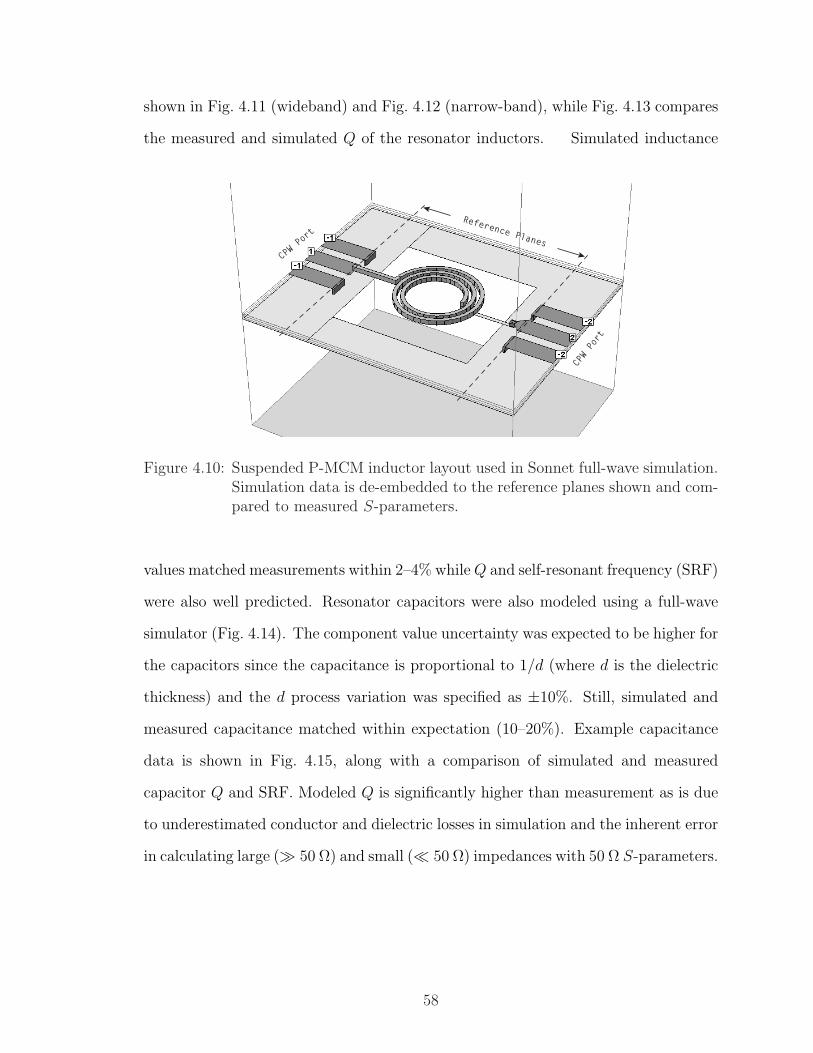
shown in Fig. 4.11 (wideband) and Fig. 4.12 (narrow-band), while Fig. 4.13 compares
the measured and simulated Q of the resonator inductors. Simulated inductance
CPW Port
CPW Port
Reference Planes
Figure 4.10: Suspended P-MCM inductor layout used in Sonnet full-wave simulation.Simulation data is de-embedded to the reference planes shown and com-pared to measured S-parameters.
values matched measurements within 2–4% while Q and self-resonant frequency (SRF)
were also well predicted. Resonator capacitors were also modeled using a full-wave
simulator (Fig. 4.14). The component value uncertainty was expected to be higher for
the capacitors since the capacitance is proportional to 1/d (where d is the dielectric
thickness) and the d process variation was specified as ±10%. Still, simulated and
measured capacitance matched within expectation (10–20%). Example capacitance
data is shown in Fig. 4.15, along with a comparison of simulated and measured
capacitor Q and SRF. Modeled Q is significantly higher than measurement as is due
to underestimated conductor and dielectric losses in simulation and the inherent error
in calculating large (À 50 Ω) and small (¿ 50 Ω) impedances with 50 Ω S-parameters.
58

Frequency (GHz)
5 10 15 20
Ind
uct
ance
(n
H)
-60
-40
-20
0
20
40
60Simulation
Measurement
Frequency (GHz)
5 10 15 20
Ind
uct
ance
(n
H)
-100
-50
0
50
100
Simulation
Measurement
Frequency (GHz)
5 10 15 20
Ind
uct
ance
(n
H)
0.5
0.6
0.7
0.8
0.9
1.0
1.1
Simulation
Measurement
Frequency (GHz)
5 10 15 20
Induct
ance
(n
H)
-150
-100
-50
0
50
100
150
Simulation
Measurement
Frequency (GHz)
5 10 15 20
Ind
uct
ance
(n
H)
-200
-100
0
100
200
Simulation
Measurement
L1
L2A
L2B
L2C
L2D
Frequency (GHz)
5 10 15 20
Ind
uct
ance
(n
H)
-300
-200
-100
0
100
200
300
Simulation
Measurement
L2E
Figure 4.11: Simulated (dashed) and measured (solid) inductance of planar spiralinductors in the MIT-LL P-MCM process. L1 is the standard inductorused in the channelizer manifold while L2x are suspended inductors usedin the resonator sections.
59

Frequency (GHz)
2 4 6 8 10
Induct
ance
(nH
)
1.6
1.8
2.0
2.2
2.4
2.6
2.8
3.0
Simulation
Measurement
Frequency (GHz)
2 4 6 8
Induct
ance
(n
H)
2.0
2.5
3.0
3.5
4.0
4.5
Simulation
Measurement
Frequency (GHz)
1 2 3 4 5 6
Induct
ance
(nH
)
3.0
3.5
4.0
4.5
5.0
5.5
6.0
Simulation
Measurement
Frequency (GHz)
1 2 3 4 5 6
Induct
ance
(n
H)
4
5
6
7
8
9
10
Simulation
Measurement
Frequency (GHz)
1 2 3 4 5 6
Ind
uct
ance
(n
H)
6
8
10
12
14
16
18
20
Simulation
Measurement
L2A
L2B
L2C
L2D
L2E
Figure 4.12: Simulated (dashed) and measured (solid) inductance of the suspendedresonator inductors over their bands of use.
60

Frequency (GHz)
2 4 6 8 10
Q
0
10
20
30
40
50
Simulation
Measurement
Frequency (GHz)
5 10 15 20
Q
0
10
20
30
40
50
Simulation
Measurement
Frequency (GHz)
2 4 6 8 10 12 14 16
Q
0
10
20
30
40
50
Simulation
Measurement
Frequency (GHz)
2 4 6 8 10 12 14
Q
0
10
20
30
40
50
60
Simulation
Measurement
Frequency (GHz)
2 4 6 8 10
Q
0
10
20
30
40
50
Simulation
Measurement
Frequency (GHz)
5 10 15 20
Q
10
15
20
25
30
35
40
45
50
Simulation
Measurement
L1
L2A
L2B
L2C
L2D
L2E
Figure 4.13: Simulated (dashed) and measured (solid) inductor Q of planar spiralinductors in the MIT-LL P-MCM process. L1 is the standard inductorused in the channelizer manifold while L2x are suspended inductors usedin the resonator sections.
61

CPW Port
CPW Port
Reference Planes
Figure 4.14: P-MCM trim-able resonator capacitor layout used in Sonnet full-wavesimulation. Simulation data is de-embedded to the reference planesshown and compared to measured S-parameters.
62
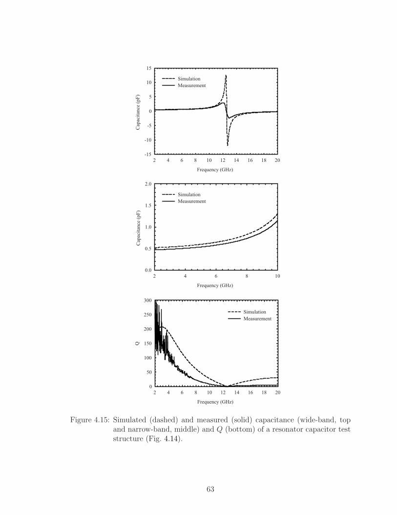
Frequency (GHz)
2 4 6 8 10 12 14 16 18 20
Q
0
50
100
150
200
250
300
Simulation
Measurement
Frequency (GHz)
2 4 6 8 10
Cap
acit
ance
(p
F)
0.0
0.5
1.0
1.5
2.0
Simulation
Measurement
Frequency (GHz)
2 4 6 8 10 12 14 16 18 20
Cap
acit
ance
(p
F)
-15
-10
-5
0
5
10
15
Simulation
Measurement
Figure 4.15: Simulated (dashed) and measured (solid) capacitance (wide-band, topand narrow-band, middle) and Q (bottom) of a resonator capacitor teststructure (Fig. 4.14).
63

Chapter 5
Higher-Order Cochlear Channelizers
In this chapter, a design method is presented for contiguous-channel multiplexing
filters with many channels covering a wide bandwidth. The circuit topology extends
previous work on cochlea-like channelizers by introducing multiple resonator-channel
filter sections. The new design provides increased stopband rejection, lower insertion
loss, and improved passband shape compared with the earlier version while retaining a
simple design method and a compact layout, and requires no post-fabrication tuning.
Results of a 3-pole, 10-channel channelizer covering 182 MHz to 1.13 GHz with 17.5%
bandwidth channels and 1.1 dB insertion loss are presented, and agree well with
theory. A discussion of the power handling of planar channelizers is also presented.
5.1 Introduction
In single-order channelizers presented in Chapters 3 and 4, the channel filters used
only series resonator sections (analogous to biological cochleas) and, as a consequence,
lacked lower stopband rejection and had non-flat passband shapes. In this chapter, we
present an improved cochlear channelizer that implements higher-order filters in each
channel. This version retains the simple inductive manifold of the single-order cochlea
channelizer but offers improved stopband rejection, passband shape, and reduced
insertion loss. A design procedure is given for a 3rd-order cochlear channelizer that
is well suited for microstrip implementation and a 10-channel design covering a 6:1
64

frequency range from 182 MHz to 1.13 GHz is presented. Such a channelizer finds
use as a pre-selector filter in wideband receivers and instantaneous spectrum activity
monitors as well as a multiplexer in wideband transmit applications.
5.2 Cochlear Channelizers Overview
5.2.1 Single-order channelizers
The first attempts to create cochlea-like RF channelizing filters were based on a
circuit topology derived from an electrical-mechanical analogy of the basilar mem-
brane. The result is a discretized, non-uniform transmission line arranged with the
highest frequency (fN) channel near the input and the lowest frequency (f1) channel
at the end of the channelizer manifold (Fig. 5.1a). The channels are coupled using
Lm(1)Lm(N)
HN(ω) H
2(ω) H
1(ω)
Z0 Z0 Z0
Lm(2)
Channel
Filter
Lm(x)∆x
fN R(x)
L(x)
C(x)∆x
1
∆x
f2 f1
V(x)
(a)
(b)
fN
f2
f1
1
∆x
Manifold
Input
Input
Figure 5.1: (a) Single-order cochlear channelizer discretized non-uniform transmissionline model. (b) Higher-order channelizer circuit model.
65

a manifold composed of small-value inductors. The electrical component values for
a single-order (single resonator) cochlear channelizer with constant fractional band-
width channels are described by
L(x)C(x) = A1eαx (5.1)
R(x)C(x) = A2e0.5αx (5.2)
Lm(x)C(x) = A3eαx (5.3)
where the four constants α, A1, A2, and A3, are determined by the channelizer’s min-
imum and maximum channel center frequencies, channel fractional bandwidth, and
the phase at the center of each channel. Such a channelizer results in a compact and
simple to design network with good upper stopband rejection for each channel. How-
ever, the single resonator channel filters have a lower stopband rejection of roughly
20 dB/decade and do not provide a tailored passband shape. The theory and design
procedure for these filters is given in [62] and results of several versions are presented
in [59] and [63].
5.2.2 Higher-Order Channelizers
Higher-order cochlear channelizers use multiple resonator filters for each chan-
nel filter while retaining the simple inductive manifold of the single-order model
(Fig. 5.1b). The higher-order channel filters provide excellent upper and lower stop-
band rejection and a flat passband shape. Because of the increased selectivity, ad-
jacent channel responses overlap much less, minimizing the power sharing between
channels and thus decreasing the insertion loss of each channel as compared with
single-order versions. For comparison, example channel responses for 3rd-order and
single-order channelizers are shown in (Fig. 5.2).
The main problem in moving from single-order to higher-order cochlear channel-
66

Frequency (MHz)
S5,0
(dB
)
-60
-50
-40
-30
-20
-10
0
100 200 500 1000 2000
Figure 5.2: Single channel responses of two channelizers, 3rd-order (solid line) andsingle-order (dashed line), covering the same bandwidth (200–1000 MHz)with 10, 18% channels.
izers lies in producing a channel filter whose input impedance behaves as a series
resonator (Zch in Fig. 5.3). At the connection node to the inductive manifold, each
channel filter should appear capacitive at frequencies below its passband and induc-
tive above its passband (Fig. 5.3). In this way, the circuit from the input port to any
fn
Zch
R
Zin
Zn
Figure 5.3: Simplified cochlear channelizer schematic at the resonant frequency ofchannel n.
particular channel node acts as a low-pass step-up matching network which trans-
forms the driving point impedance at the resonating channel filter node (Zn) to the
channelizer input impedance (Zin typically 50 Ω). The required channel filter input
impedance (Zch) properties are discussed in the following section.
67

5.3 Circuit Design
The channelizer design procedure includes determining the number and bandwidth
of each channel, synthesis of each channel filter, and designing the manifold.
5.3.1 Design Parameters
The design process starts with choosing the desired frequency range, channel frac-
tional bandwidth, and crossover point for adjacent channels. The crossover point
is chosen as 2 to 3 dB below each channel’s maximum response. This creates the
required amount of inter-channel coupling for the cochlea-like response and achieves
a wideband input match by absorbing nearly all of the power in the total channelizer
bandwidth. The number of channels N needed to cover the required bandwidth is
given by
N ' 1 +
ln
(fN
f1
)
ln
(1 + ∆/2
1−∆/2
) (5.4)
where f1 and fN are the minimum and maximum channel center frequencies, respec-
tively, and ∆ is the fractional bandwidth of each channel defined from the crossover
points of adjacent channels. The channel center frequencies are then chosen to cover
the desired frequency range, starting with the lowest channel center frequency f1 and
continuing to the highest channel center frequency fN , as
fn+1 = fn
(1 + ∆/2
1−∆/2
), 1 ≤ n ≤ N − 1. (5.5)
5.3.2 Channel Filter Synthesis
The most important feature of each channel filter is its input impedance behavior
over the entire channelizer bandwidth. In particular, each filter must present a near-
68

open circuit at its input port (Zch) for frequencies far above and below its center
frequency (Fig. 5.4), appearing capacitive below its passband (Zin → −j∞ Ω) and
inductive above its passband (Zin → +j∞ Ω).
Zch Z0
f >> f0
f << f0
Figure 5.4: Required channel filter input impedance characteristic (Smith Chart) andthe corresponding bandpass filter prototype for a cochlear channelizer(response for 3rd-order shown).
To understand why, consider the single-order circuit (Fig. 5.1a) as a low-pass
transmission line with shunt-connected series resonant circuits. An input signal with
frequency f2 enters the input and first encounters resonators tuned to higher frequen-
cies. These branches appear capacitive and, with the inductive manifold, produce a
low-pass ladder network of shunt capacitors and series inductors. The signal prop-
agates on this lumped LC transmission line until it reaches a series resonator with
resonant frequency f2. At this frequency, the resonator appears as a pure resistance
R and absorbs the f2 signal power.
If the series resonators are replaced with parallel types, the signal f2 first encoun-
ters a near-short circuit (small inductive reactance) and is mostly reflected toward
the input (Fig. 5.5a). Also, nearly as destructive to the channelizer operation are
69
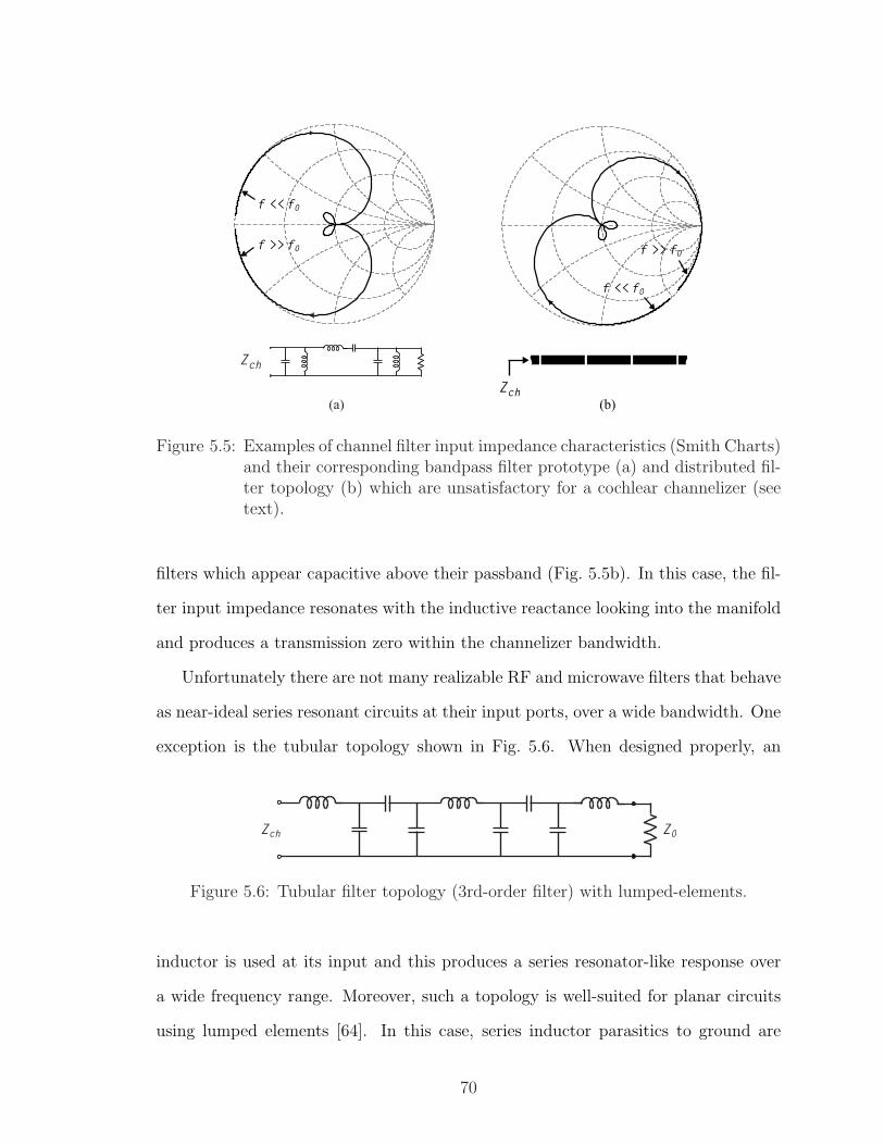
(a)
Zch
f >> f0
f << f0
(b)
Zch
f >> f0
f << f0
Figure 5.5: Examples of channel filter input impedance characteristics (Smith Charts)and their corresponding bandpass filter prototype (a) and distributed fil-ter topology (b) which are unsatisfactory for a cochlear channelizer (seetext).
filters which appear capacitive above their passband (Fig. 5.5b). In this case, the fil-
ter input impedance resonates with the inductive reactance looking into the manifold
and produces a transmission zero within the channelizer bandwidth.
Unfortunately there are not many realizable RF and microwave filters that behave
as near-ideal series resonant circuits at their input ports, over a wide bandwidth. One
exception is the tubular topology shown in Fig. 5.6. When designed properly, an
Zch Z0
Figure 5.6: Tubular filter topology (3rd-order filter) with lumped-elements.
inductor is used at its input and this produces a series resonator-like response over
a wide frequency range. Moreover, such a topology is well-suited for planar circuits
using lumped elements [64]. In this case, series inductor parasitics to ground are
70

conveniently absorbed into the ends of the coupling capacitor pi-networks (Fig. 5.6).
To synthesize each channel filter one starts with the prototype bandpass filter
(Fig. 5.7a), whose circuit elements are given by
Lk =
gkR1
∆ ω0
k odd
∆ R1
gkω0
k even
(5.6)
and,
Ck =
∆
gkω0R1
k odd
gk
∆ ω0R1
k even
(5.7)
where ∆ is the filter’s fractional bandwidth,
∆ =ω2 − ω1
ω0
,
and ω0 is the filter passband center frequency, ω0 =√
ω1ω2, where ω1 and ω2 define
the filter’s passband limits [17]. For a channelizer input impedance (Zin) of 50 Ω,
channel filters with input impedance (Zch = R1) from 5 to 20 Ω (all filters use the
same R1) result in reasonable component values and good input return loss over the
channelizer bandwidth. To simplify the design process and accommodate an off-the-
shelf inductor value L, one can use (5.6) with L1 = L to set the channel filter’s input
resistance (R1) within a desired range (Fig. 5.7a). One can also slightly vary the
lumped-element prototype parameters (gk) (and thus the filter shape) to obtain a
suitable inductance L for a needed channel filter R1.
71

(a)
(b)
(c)
C1'L L L2C
2'' 2C
2'' C
3'
C12
C23
R1
R1
L L LC1-C
12-C
12
C12
C23
-C23
R1
R1
-C23
C3
L1
C1
L2
L2
C2
C2
R1
R1
C2'
K12
K23
(f)
(d)
(e)
L L
R1
R2
L
Ca
Cb
Cc
Cd
Ce
Cf
Cg
R1
R2
C12
C23
C1'
Cm
L L L2C2'' 2C
2'' C
3''
Lm
C1'L L L2C
2'' 2C
2'' C
3'
C12
C23
Cm
R1
R2
Zch
=
Figure 5.7: Channel filter schematics showing network transformations used to arriveat a channel filter with the desired input impedance characteristics.
72

For the odd-order filter with symmetric lumped-element prototype values,
K12 = K23 =
√L
C2
(5.8)
and the inverter capacitors are given by,
C12 = C23 =1
ω0K12
. (5.9)
The second resonator capacitor is chosen to provide the correct resonator impedance
level while maintaining identical inductor values (Fig. 5.7b),
C′2 =
L2
K212
. (5.10)
Next, the inverter capacitors are absorbed into the network (Fig. 5.7c),
C′1 =
(1
C1
− 1
C12
)−1
(5.11)
C′3 =
(1
C3
− 1
C23
)−1
(5.12)
C′′2 =
(1
C′2
− 1
C12
− 1
C23
)−1
. (5.13)
A matching section is then added to the output (Fig. 5.7d) to transform the output
impedance to the desired channel output impedance R2 (typically 50 Ω), using
Cm =
√R2/R1 − 1
ω0R2
(5.14)
Lm =R2
2Cm
1 + (ω0R2Cm)2 (5.15)
73
and the third resonator capacitor is modified to maintain identical inductors in each
resonator (Fig. 5.7e),
C′′3 =
L
L− Lm
C′3. (5.16)
A Tee (star) to Pi (delta) transformation is then performed on the sections coupling
the second and third resonators, producing the desired tubular filter network, where
(Fig. 5.7f)
Ca =C′1C12
C′1 + 2C
′′2 + C12
(5.17)
Cb =C′12C
′′2
C′1 + 2C
′′2 + C12
(5.18)
Cc =2C
′′2 C12
C′1 + 2C
′′2 + C12
(5.19)
Cd =2C
′′2 C23
2C′′2 + C
′′3 + C23
(5.20)
Ce =2C
′′2 C
′′3
2C′′2 + C
′′3 + C23
(5.21)
Cf =C′′3 C23
2C′′2 + C
′′3 + C23
(5.22)
and finally (Fig. 5.7f),
Cg ≡ Cm (for nomenclature). (5.23)
Note that this synthesis relies on ideal inverter sections between the second and
third resonators, and an ideal impedance matching section at the output port and
is therefore approximate. For a channel filter fractional bandwidth above 10%, some
adjustment is required to maintain the desired passband ripple and 3-dB points. In
practice, one can use these synthesized circuit element values as a starting point in
an implementation with real microstrip and lumped components, and tune the circuit
using simulation tools to achieve the desired passband response. Synthesis of channel
filters other than 3rd-order follows the same basic procedure.
74

5.3.3 Manifold Design
Higher-order channelizers use the same inductive manifold employed in single-
order versions (Fig. 5.1a). In the higher-order case, the channel filters are designed
for a termination on the manifold port with R1 = R (see Fig. 5.3) and R2 = 50 Ω.
For constant fractional bandwidth channels, the manifold inductors are exponentially
scaled with distance (and thus frequency) along the channelizer, and using (5.2)–(5.3),
are given by
Lm(x) = RA3
A2
e12αx = L0e
ax (5.24)
where L0 = RA3
A2and a = α/2. In terms of (integer) channel number n, the coupling
inductances are
Lm(n) = L0ea(1−n/N), 1 ≤ n ≤ N. (5.25)
To design the manifold, one uses the same procedure described in [62] for a single-
order channelizer using series resonators with input impedance R. The higher-order
channel filter sections (with R1 = R) are then coupled with the same manifold induc-
tances. Alternatively, one can use a circuit simulator to find the coupling inductors,
eliminating the need to program and iterate the numerical procedure in [62]. Once the
channel filters are designed and connected by series inductances Lm(n), one varies L0
and a in simulation to achieve the best input return loss. As a starting point, Lm(n)
should be chosen to give a reactance (X = 2πfLm) of 3–8 Ω at the lowest channel
center frequency (f1) and 10–20 Ω at the highest channel center frequency (fN) with
an exponential scale factor a of 0.3 to 1.0. These values are based on single-order
designs and result in channelizers with Zin centered near 50 Ω [62].
75

5.4 Experimental Results
5.4.1 Design, Layout, and Simulation
A 10-channel channelizer (N = 10) is designed to cover 200 MHz to 1 GHz
(Fig. 5.8). A desired channel 3-dB fractional bandwidth of 18% in (5.4) indicates
Port N
50 Ω
C0
Ca(N)
L(N)
Lm(N)
50 Ω
Input
(Port 0)
50 Ω
R0
Cb(N)Cc(N)
Cd(N)
Ce(N)Cf(N)
Cg(N)
L(N)
L(N)
Ca(2)
L(2)
Cb(2)Cc(2)
Cd(2)
Ce(2)Cf(2)
Cg(2)
L(2)
L(2)
Ca(1)
L(1)
Cb(1)Cc(1)
Cd(1)
Ce(1)Cf(1)
Cg(1)
L(1)
L(1)
Lm(2) Lm(1)
Port 2 Port 1
Figure 5.8: Circuit schematic diagram of a 3rd-order cochlear channelizer.
that 10 channels are required, and the channel filter center frequencies are calculated
using (5.5). The inductors are chosen using (5.6) with the prototype (gk) values for
a 0.1-dB ripple Chebyshev passband for the channel filters (note that the ∆ = 0.12
specifies the ripple bandwidth). Commercially available inductor values ranging from
120 nH to 22 nH for 200–1000 MHz result in a filter (Zch) input resistance R1 of
' 17 Ω. Each channel filter (Fig. 5.7f) is then synthesized using (5.6)–(5.23) with
R1 = 17 Ω and R2 = 50 Ω. With an Lm(10) = 2.4 nH (for channel 10) chosen to
76
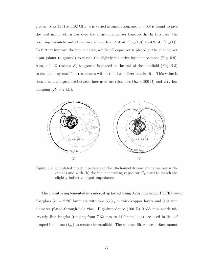
give an X ' 15 Ω at 1.02 GHz, a is varied in simulation, and a = 0.8 is found to give
the best input return loss over the entire channelizer bandwidth. In this case, the
resulting manifold inductors vary slowly from 2.4 nH (Lm(10)) to 4.9 nH (Lm(1)).
To further improve the input match, a 2.75 pF capacitor is placed at the channelizer
input (shunt to ground) to match the slightly inductive input impedance (Fig. 5.9).
Also, a 1 kΩ resistor R0 to ground is placed at the end of the manifold (Fig. B.3)
to dampen any manifold resonances within the channelizer bandwidth. This value is
chosen as a compromise between increased insertion loss (R0 < 500 Ω) and very low
damping (R0 > 2 kΩ).
(b)
C0 = 2.75 pF
(a)
C0 = 0 pF
100 MHz
2 GHz
100 MHz2 GHz
Figure 5.9: Simulated input impedance of the 10-channel 3rd-order channelizer with-out (a) and with (b) the input matching capacitor C0, used to match theslightly inductive input impedance.
The circuit is implemented in a microstrip layout using 0.787 mm height PTFE/woven
fiberglass (εr = 2.20) laminate with two 53.3 µm thick copper layers and 0.51 mm
diameter plated-through-hole vias. High-impedance (100 Ω) 0.635 mm width mi-
crostrip line lengths (ranging from 7.62 mm to 11.9 mm long) are used in lieu of
lumped inductors (Lm) to create the manifold. The channel filters use surface mount
77

technology (SMT) devices, including Coilcraft Midi Spring1 air coil inductors (L)
and Dielectric Laboratories C062 multilayer capacitors (Cb, Ce, Cg), all with 2% or
better tolerance. The remaining shunt capacitors (including C0) are composed of the
microstrip metal layer (top plates) and ground plane (bottom plates). The output of
each channel filter (after Cg in Fig. 5.7f) is routed to an edge-launch SMA connec-
tor using 2.54 mm width 50 Ω microstrip lines with simulated losses of 0.56 dB/m
at 1 GHz and 0.22 dB/m at 200 MHz. A close-up view of a single channel’s layout
5.50 in
6.50 in
Ch 1
Ch 3
Ch 5
Ch 7
Ch 9
Ch 2
Ch 4
Ch 6
Ch 8
Ch 10
C0
R0
Z0 = 50 Ω
Lm(10)
Figure 5.10: Photograph of a 10-channel 3rd-order cochlear channelizer with centerfrequencies ranging from 200 MHz to 1022 MHz. The channel filters arestaggered on the sides of the inductive manifold. The input port is inthe center of the lower substrate edge while the two sets of five outputports occupy the left and right board edges fed by microstrip lines fromchannel outputs.
(channel 5) is shown in Fig. 5.11. The channelizer manifold and filter lumped element
1Coilcraft Inc., Cary, IL USA2Dielectric Laboratories, Inc., Cazenovia, NY USA
78
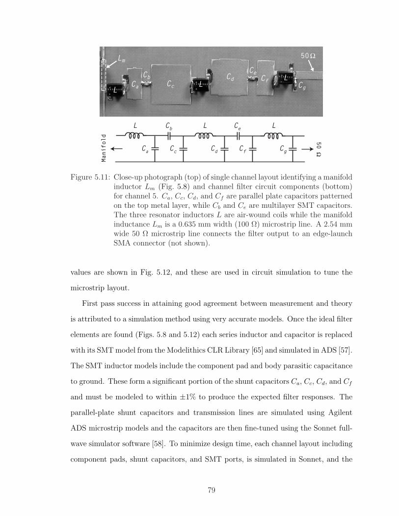
Lm
LL
LCa
CbCc
Cd
CeCf
Cg
50 Ω
L LL
Ca
Cb
Cc
Cd
Ce
Cf
Cg
Manifold
50
Ω
Figure 5.11: Close-up photograph (top) of single channel layout identifying a manifoldinductor Lm (Fig. 5.8) and channel filter circuit components (bottom)for channel 5. Ca, Cc, Cd, and Cf are parallel plate capacitors patternedon the top metal layer, while Cb and Ce are multilayer SMT capacitors.The three resonator inductors L are air-wound coils while the manifoldinductance Lm is a 0.635 mm width (100 Ω) microstrip line. A 2.54 mmwide 50 Ω microstrip line connects the filter output to an edge-launchSMA connector (not shown).
values are shown in Fig. 5.12, and these are used in circuit simulation to tune the
microstrip layout.
First pass success in attaining good agreement between measurement and theory
is attributed to a simulation method using very accurate models. Once the ideal filter
elements are found (Figs. 5.8 and 5.12) each series inductor and capacitor is replaced
with its SMT model from the Modelithics CLR Library [65] and simulated in ADS [57].
The SMT inductor models include the component pad and body parasitic capacitance
to ground. These form a significant portion of the shunt capacitors Ca, Cc, Cd, and Cf
and must be modeled to within ±1% to produce the expected filter responses. The
parallel-plate shunt capacitors and transmission lines are simulated using Agilent
ADS microstrip models and the capacitors are then fine-tuned using the Sonnet full-
wave simulator software [58]. To minimize design time, each channel layout including
component pads, shunt capacitors, and SMT ports, is simulated in Sonnet, and the
79

Ind
uct
ance
(n
H)
20
40
60
80
100
120
Ind
uct
ance
(n
H)
2.0
2.5
3.0
3.5
4.0
4.5
5.0
L
Lm
Channel Number
10
Cap
acit
ance
(p
F)
0.0
0.4
0.8
1.2
1.6
Cap
acit
ance
(p
F)
0
5
10
15
20
25
Cb
Ce
Ca
Cc
Cd
Cf
Cg
987654321
Figure 5.12: Lumped element component values for the 10-channel 200–1000 MHz3rd-order cochlear channelizer (not shown, C0 = 2.75 pF).
80

resulting S-parameters are exported to Agilent ADS and simulated together with the
Modelithics component models. If necessary, lumped shunt capacitance is added or
subtracted until agreement is obtained between the modeled and ideal filter responses.
Then, the Sonnet model is modified to provide for the changed capacitance(s) and the
simulation is redone. Using the combination of the Modelithics component library,
ADS microstrip models, and Sonnet full-wave simulations, each channel took 2–4
iterations to match the expected filter response and the final component values and
layout dimensions are found.
81

5.4.2 Measurements
The channelizer’s S-parameters are measured using an Agilent E5071B vector net-
work analyzer (VNA). A 2-port short-open-load-thru (SOLT) coaxial line calibration
sets the reference planes at the coaxial connectors. Each channel’s transmission re-
sponse with respect to the channelizer input port (Sn,0, 1 ≤ n ≤ 10) is measured
by connecting VNA port 1 to the channelizer input (port 0) and VNA port 2 to the
nth channel output (port n) while all other channel outputs are terminated in a 50 Ω
load. The channelizer’s input return loss (S0,0) measurement is obtained in the same
way (each channel output terminated in 50 Ω).
The measured and simulated S-parameters of the 10-channel channelizer are
shown in Fig. 5.13 and Fig. 5.14 and a summary of channel characteristics appears in
Table 5.1. The channels have an average fractional bandwidth of 17.5% and an aver-
Frequency (MHz)
100 200 500 1000 2000
Sn
,0 (
dB
)
-60
-50
-40
-30
-20
-10
0
Figure 5.13: Measured (solid) and simulated (dashed) transmission response (Sn,0) ofeach channel of the 3rd-order cochlear channelizer.
age insertion loss of 1.12 dB at each channel’s center frequency. The measurements
agree very well with the simulations without any post-fabrication tuning.
82

Frequency (MHz)
100 200 500 1000 2000
S0
,0 (
dB
)
-25
-20
-15
-10
-5
0
Figure 5.14: Measured (solid) and simulated (dashed) return loss (S0,0) of the 3rd-order cochlear channelizer.
A single channel’s (channel 5) narrow-band transmission response (S5,0) and group
delay are shown in Fig. 5.15 along with the simulated response for a stand-alone 3-
pole filter with the topology shown in Fig. 5.7f. Compared with the stand-alone filter,
the channelizer response has slightly higher rejection and an altered phase response.
This results in an additional 2 ns of group delay at the center of channel 5.
Measurements of Sn,m for n 6= m are also performed to characterize the channel-
izer’s channel-to-channel isolation. Isolation between channel 1 and channels 2–10
is given by S1,2...10 (Fig. 5.16) while isolation between channel 10 and channels 1–9
is given by S10,1...9 (Fig. 5.17). A particular channel’s isolation to other channels
closely follows its stopband response for channels located on the opposite side of the
manifold; in this case, the coupling between different channels is through the induc-
tive manifold only. However, a small amount of electromagnetic coupling occurs for
channels on the same side of the manifold. This is seen as a rise in Sn,m in the upper
stopband of channel 1 (Fig. 5.16) and in the lower stopband of channel 10 (Fig. 5.17).
83
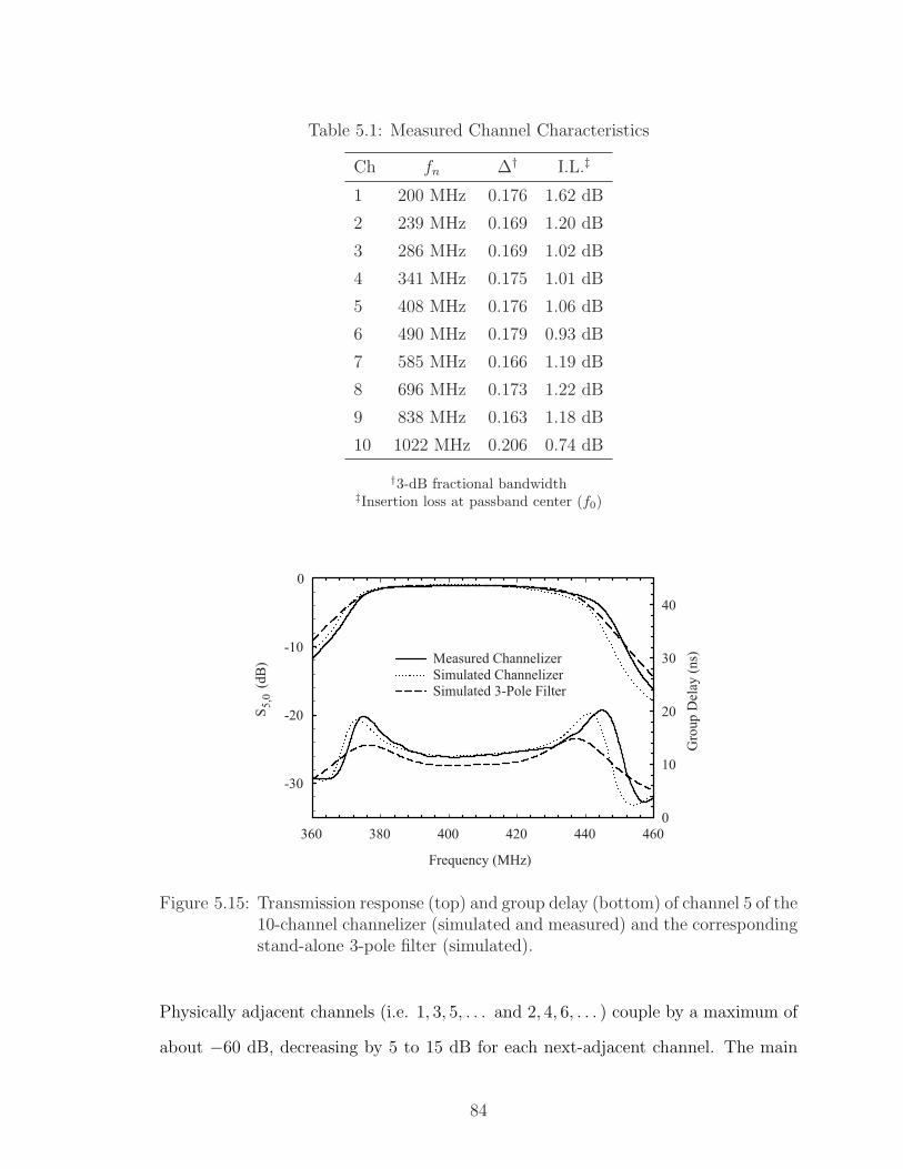
Table 5.1: Measured Channel Characteristics
Ch fn ∆† I.L.‡
1 200 MHz 0.176 1.62 dB
2 239 MHz 0.169 1.20 dB
3 286 MHz 0.169 1.02 dB
4 341 MHz 0.175 1.01 dB
5 408 MHz 0.176 1.06 dB
6 490 MHz 0.179 0.93 dB
7 585 MHz 0.166 1.19 dB
8 696 MHz 0.173 1.22 dB
9 838 MHz 0.163 1.18 dB
10 1022 MHz 0.206 0.74 dB
†3-dB fractional bandwidth‡Insertion loss at passband center (f0)
Frequency (MHz)
360 380 400 420 440 460
S5
,0 (
dB
)
-30
-20
-10
0
Gro
up
Del
ay (
ns)
0
10
20
30
40
Measured Channelizer
Simulated Channelizer
Simulated 3-Pole Filter
Figure 5.15: Transmission response (top) and group delay (bottom) of channel 5 of the10-channel channelizer (simulated and measured) and the correspondingstand-alone 3-pole filter (simulated).
Physically adjacent channels (i.e. 1, 3, 5, . . . and 2, 4, 6, . . . ) couple by a maximum of
about −60 dB, decreasing by 5 to 15 dB for each next-adjacent channel. The main
84

Frequency (MHz)
100 200 500 1000 2000
-100
-80
-60
-40
-20
0
S1,3
S1,5
S1,0
Sn,m
(d
B) S1,2
S1,3
Figure 5.16: Measured S1,0 (solid line) along with S1,2...10 (dashed lines) which giveschannel 1’s (n = 1) isolation to other channels (m = 2 . . . 10). Isolationfollows the upper stopband skirt of channel 1 with reduced isolationto channels located on the same side of the manifold (n = 3, 5, 7, 9)(Fig. B.3).
coupling mechanism between adjacent channels is electromagnetic coupling between
the microstrip shunt capacitors. The largest shunt capacitors for each channel have
lengths ranging from 6.6 mm (1 GHz) to 17.8 mm (200 MHz) or about 0.02–0.03 λg
(guided wavelength) and are separated by a minimum of 7.6 mm (10× the substrate
height) at the lowest frequency channels.
Since each filter has higher rejection in its upper stopband, lower frequency chan-
nels feature higher rejection of higher frequency channels. This is illustrated for
three channel center frequencies (of channels 1, 5, and 10) in Fig. 5.18 which shows
the power level of a particular frequency appearing at each channel port (the power
is normalized so that a particular channel has 0 dB of rejection at its own center
frequency).
85

Frequency (MHz)
100 200 500 1000 2000
Sn,m
(d
B)
-100
-80
-60
-40
-20
0
S10,8
S10,6
S10,0
S10,8
S10,9
S10,6
Figure 5.17: Measured S10,0 (solid line) along with S10,1...9 (dashed lines) which giveschannel 10’s (n = 10) isolation to other channels (m = 1 . . . 9). Isolationfollows the lower stopband skirt of channel 10 with reduced isolationto channels located on the same side of the manifold (n = 2, 4, 6, 8)(Fig. B.3).
Channel Number
1 2 3 4 5 6 7 8 9 10
Rej
ecti
on (
dB
)
0
20
40
60
80
100
f1
f5
f10
Figure 5.18: Measured rejection of channel 1, 5, and 10 center frequencies at all chan-nel output ports.
86

5.4.3 Loss Analysis
To understand the loss mechanisms, we consider how power at a single frequency
is distributed throughout the channelizer. At the center frequency of channel 5 (408
MHz), the percentage of the input power appearing at each output port is calculated
from each channel’s measured |Sn,0|2. Likewise, the reflected power at the channelizer
input is given by |S0,0|2. At 408 MHz, 78.3% of the power arrives at the channel
5 output (1.06 dB insertion loss), 0.937% appears at all other channel outputs, and
0.987% is reflected at the channelizer input (20.1 dB input return loss). Summing
these powers results in 80.2% of the input power. Thus, the filter dissipates 19.8%
of the input power corresponding to an effective loss of 0.96 dB. The dissipation is
Table 5.2: Sample Channel Power Distribution for Channel 5
Power (%)
Channel 5 Output 78.3 (−1.06 dB)
Sum of Channel 1–4, 6–10 Outputs 0.937
Reflected at Input 0.987
Sum of all Power Contributions 80.2
Power Dissipated 19.8
primarily due to the channel filter inductor losses. Channel filter inductor (L) un-
loaded Q ranges from 130–150 at the channel center frequencies, while capacitor and
manifold inductor (Lm) unloaded Qs range from 600–1200 and 200–350, respectively.
5.4.4 Power Handling for Transmit Applications
All channelizer components are passive and isotropic, and therefore the circuit’s
S-parameters are reciprocal. Thus, the channelizer can also be used as a transmit
multiplexer where the individual channel ports are connected to transmitter outputs
and the common manifold port serves as the multiplexer output.
87

The SMT components used in each channel filter limit the channelizer’s single-tone
average and peak power handling capability. The largest value inductor (L(1)=120 nH)
used has the lowest maximum r.m.s. current rating of 1.5 A (it has the largest number
of turns, thus the most resistance and loss). From simulation, this current corresponds
to a maximum channelizer single-tone average input power of 27 W. The channelizer’s
capacitors must also be operated below their dielectric breakdown voltage. Of all the
capacitors used, the SMT units have the lowest maximum voltage rating of 625 V
corresponding to a channelizer peak input power of 60 W.
The inductive manifold composed of thin microstrip lines imposes an upper limit
on the channelizer’s multi-tone power handling capability. The maximum tempera-
ture rise ∆T of a microstrip line conductor is given by [66]
∆T =Pih
(1− 10−
Al10
)
lwk(5.26)
where l and w are the line length and width, h is the substrate height (all in [m]), Pi is
the incident power (in [W]), k is the substrate thermal conductivity (in [Wm−1K−1]),
and A is the transmission line loss (in [dB/m]). The copper-clad PTFE/woven fiber-
glass substrate used in this design is rated for operation at a maximum of 125C. This
limit is first reached for the 0.635 mm wide manifold section nearest to the common
port since this section carries the power of all 10 channels. For this channelizer, the
maximum allowable average power is 14 W per channel (140 W total) at 25C ambi-
ent (100C temperature rise) and 5.6 W per channel (56 W total) at 85C ambient
(40C temperature rise). The channelizer can be built on AlN or other substrates
with higher thermal conductivity to increase its average power handling capability.
We have improved cochlea-like channelizers by using 3rd-order channel filters with
the appropriate input impedance characteristic. The new channelizers feature chan-
nels with improved rejection, flat passband shape, and reduced insertion loss, and
88

retain the simple inductive manifold of earlier cochlear channelizers. The design pro-
cedure is easily extended to include 4th and higher-order channel filters.
5.5 Distributed 2nd-order Channelizer Simulations
A distributed-element cochlear channelizer is attractive for higher microwave fre-
quencies. Above about 2 GHz, transmission line resonators become reasonably small
allowing the realization of compact wideband channelizers. In addition, simulation
is more straightforward and fabrication of multiple samples is possible in a mono-
lithic process. To that end, design of a second-order planar channelizer covering 2
to 6 GHz was undertaken. Simulations were done of using end-coupled microstrip
resonator filters. In the course of moving the design from ideal elements to a physical
layout, a problems was encountered that shed light on the channel filter properties
required for the cochlear channelizer topology. While this experiment did not result
in a successful design, it demonstrates the importance of the maintaining the chan-
nel filter’s series resonator-like wideband input impedance characteristics within a
cochlear channelizer, and is included here to offer insight for further work.
5.5.1 Design Equations
At first glance, end-coupled λ/2 resonator filters appear to be a good candidate for
use in a cochlear channelizer. The open-ended resonators, which behave like parallel
resonant circuits, are coupled together through admittance inverters which transform
their properties to series resonator-like response (i.e. they appear as open circuits in
the filter stop-bands).
A distributed-element channelizer design follows the same procedure as the lumped-
element one described earlier. One designs the individual filter sections with an input
(manifold side) impedance less than 50 Ω, then designs a manifold of inductors (or
89

high impedance transmission line segments) using the single-order channelizer theory.
One additional problem comes with distributed filter implementations. If the
channelizer covers more than about one octave, one must eliminate re-entrant filter
responses that interfere with other channel filters. These spurious passbands are due
to higher-order resonator responses and generally appear at 2mf0 for λ/2 types and at
3mf0 for λ/4 resonators (m = 1, 2, 3 . . . ), where f0 is the passband center frequency.
In parallel-coupled filters using λ/4 resonators, the first spurious passband appears
closer to 2f0 due to a difference in even and odd mode phase velocities in the coupled
sections [67]. In all of these distributed filters, this periodic behavior also decreases
filter upper stop-band rejection since the transmission response begins to rise after
the first pass-band instead of maintaining a monotonically decreasing skirt (as in
lumped-element filters).
For end-coupled λ/2 filters, the spurious resonance problem is easily solved by
used stepped impedance resonators (SIR). These resonators use alternating sections
of low impedance (Z1) and high impedance (Z2) transmission lines. Analysis of
the resonance condition of such a resonator shows that its spurious-free bandwidth
increases with the ratio of the two impedances (Z2/Z1). Filters using these resonators
are designed using the standard procedure for direct-coupled resonator filters given in
[17] and [68] with modified expressions for the resonator susceptance slope parameters
given in [69] and [70]. Other suggested techniques for spurious passband suppression
that look promising for planar designs are given in [71] and [72].
The general model for a second-order (N = 2) filter is shown in Fig. 5.19a and
the transmission line implementation of the model elements is shown in Fig. 5.19b,c.
The lumped capacitors (Cn,n+1) are realized with either narrow microstrip gaps, in-
terdigital capacitors, metal-insulator-metal (MIM) capacitors in a multi-layer planar
process, or SMT devices. An example layout is shown in Fig. 5.23b along with a
uniform impedance version for comparison (Fig. 5.23a).
90

ZLJ01 B1 J12 B2 J23ZS
(a)
Za, θn,n+1'
Cn,n+1
Zb, θn,n+1
(b)
θ, Z1
θ, Z1
2θ, Z2
(c)
Figure 5.19: (a) Direct-coupled resonator filter model (N = 2) with ideal inverters(Jn,n+1) and parallel resonators (Bk), (b) inverter implementations withtransmission lines and a series capacitor, and (c) stepped impedanceresonator (SIR) with equal line lengths.
(a)
(b)
Z0, θZ0 Z0Z0, θ
Z1, θZ0 = ZS Z0 = ZL
Z1, θ
Z2, 2θ
Z1, θ Z1, θ
Z2, 2θ
Figure 5.20: Second-order end-coupled λ/2 resonator filters using microstrip (a) uni-form impedance and (b) stepped impedance resonators (SIR).
The design equations for the 2nd-order λ/2 SIR filter are summarized below, using
the definitions in Table 5.3. For an SIR composed of two low impedance (Z1) segments
of length θ on each end and one middle, high impedance segment (Z2) of length 2θ,
91

Table 5.3: SIR Filter Impedance Definitions
ZS ≡ Filter input impedance [Ω]
ZL ≡ Filter output impedance [Ω]
Z1 ≡ Resonator impedance (low) [Ω]
Z2 ≡ Resonator impedance (high) [Ω]
the expression for the length is given by
θ = tan−1√
k (5.27)
where k is the ratio of the impedances,
k =Z1
Z2
(5.28)
and the frequency of the first spurious response fs1 increases with greater ratios of
Z2 to Z2 (i.e. smaller k) [69],
fs1
f0
=π
2 tan−1√
k. (5.29)
The susceptance slope parameter of this SIR is
b = 2θYres =2θ
Z1
(5.30)
where Yres is the admittance of the coupled resonator (the low impedance section in
this case since it appears at the ends of each resonator). Using (5.30) in the standard
form of direct-coupled resonator filters with J-inverter-coupled parallel resonators
92
[17, 40] gives the inverter values
Jn,n+1 =
√∆ b
ZSg0g1
n = 0
∆ b√g1g2
n = 1
√∆ b
ZLg0g1
n = 2
(5.31)
The inverters can be realized by a Pi-network of capacitors or with the transmission
line and capacitor network shown in Fig. 5.19b. The latter network’s transmission line
lengths are negative for positive capacitance values. This circuit is attractive since
the negative transmission line lengths are absorbed in adjacent lines of the same
characteristic impedance. In addition, this inverter can be designed with arbitrary
impedances for each transmission line. For example, the input inverter J01 is designed
with a Za = 50 Ω (the filter input impedance) and Zb = Z1 (the low impedance
resonator section). The transmission line lengths are given by [73],
θ′n,n+1 =1
2(pn,n+1 + qn,n+1) , n = 0, 1, 2 (5.32)
θn,n+1 =1
2(pn,n+1 − qn,n+1) , n = 0, 1, 2 (5.33)
where p, q, and B are
pn,n+1 =
− tan−1[(ZS/Z1 + 1) B01
]n = 0
− tan−1(2B12
)n = 1
− tan−1[(ZL/Z1 + 1) B23
]n = 2
(5.34)
93

qn,n+1 =
− tan−1[(ZS/Z1 − 1) B01
]n = 0
0 n = 1
− tan−1[(ZL/Z1 − 1) B23
]n = 2
(5.35)
Bn,n+1 =
[(J01Z1)
2 − 1](ZS/Z1)
2 + (J01Z1)−2 − 1
−1/2n = 0
[(J12Z1)
2 − 1]+ (J12Z1)
−2 − 1−1/2
n = 1
[(J23Z1)
2 − 1](ZL/Z1)
2 + (J23Z1)−2 − 1
−1/2n = 2
(5.36)
and the inverter capacitor values are given by
Cn,n+1 =Bn,n+1
ω0Z1
, n = 0, 1, 2. (5.37)
5.5.2 Simulation Results
A 10-channel, 2 to 6 GHz channelizer was designed using SIR channel filters. The
filter λ/2 resonators used alternating sections of Z1 = 20 Ω and Z2 = 90 Ω placing
the first spurious filter passband at approximately 3.6f0. For the lowest frequency
channel centered at 2 GHz, the first re-entrant response occurs above 7 GHz (Fig. 5.21)
without significantly affecting the desired passband shape (Fig. 5.22). Each channel
was designed with ∆ = 12.2% and an input impedance of 20 Ω. The manifold
used an L0 of 0.400 nH and exponential taper of a = 0.5. A proposed layout
for this channelizer is shown in Fig. 5.23. The manifold inductors are implemented
with high impedance microstrip segments and series capacitances are done with MIM
capacitors. A full-wave simulation was done of each resonator section using Sonnet
and the results imported into ADS for a linear circuit simulation with ideal manifold
and coupling elements used to tune parasitic effects. Once the channel filters and
94
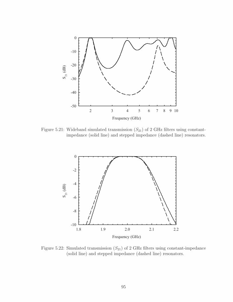
Frequency (GHz)
2 3 4 5 6 7 8 9 10
S21 (
dB
)
-50
-40
-30
-20
-10
0
Figure 5.21: Wideband simulated transmission (S21) of 2 GHz filters using constant-impedance (solid line) and stepped impedance (dashed line) resonators.
Frequency (GHz)
1.8 1.9 2.0 2.1 2.2
S21 (
dB
)
-10
-8
-6
-4
-2
0
Figure 5.22: Simulated transmission (S21) of 2 GHz filters using constant-impedance(solid line) and stepped impedance (dashed line) resonators.
95

Input
(50 Ω)
Stepped-Z
Resonator
Filter
(n=2)
50 Ω
M.S.
High-Z
Manifold
Figure 5.23: Proposed layout for second-order cochlear channelizer using end-coupledstepped-impedance resonator filters.
manifold were connected in simulation a critical problem with the channel filter’s
response was identified.
The end-coupled λ/2 filters require negative-value transmission lines for the in-
verter sections (Fig. 5.19b) located in between each resonator as well as at the input
and output ports. For inter-resonator coupling, the negative transmission lines are
physically absorbed into the circuit by reducing the resonator lengths. At the in-
96

put and output, however, no physical transmission line exists. This is dealt with
by setting the inverter transmission line impedance equal to the port impedance.
Thus, any length of matched transmission does not alter the magnitude of the filter’s
transmission response, and the length can be conveniently set to zero (or some other
convenient length). However, this does alter the filter’s phase response by a negative
amount equal to the inverter line section (plus any additional physical line length
used). This is seen on a Smith chart as rotating S11 negative θ′01 degrees (clockwise),
moving the high frequency response from a near-open circuit into the capacitive re-
gion (Fig. 5.5b). The effect of this impedance transformation on the channelizer
circuit is an in-band resonance with the inductive impedance seen at the manifold,
producing a transmission zero at in the channelizer bandwidth. This is clearly seen
in the simulated transmission plots in Fig. 5.24. By placing ideal negative transmis-
Frequency (GHz)
2 3 4 5 6 7 8 9 10
S21 (
dB
)
-60
-50
-40
-30
-20
-10
0
Figure 5.24: Simulated transmission (S21) of each channel of a 2nd-order channelizerusing end-coupled resonator filters (θ01 = 0) at filter input).
sion line lengths at the filter inputs (the manifold-filter interfaces), as in the ideal
circuit model, the desired channelizer response is obtained as shown in Fig. 5.25.
97

Unfortunately, a solution to this problem has not yet been found. An obvious first
Frequency (GHz)
2 3 4 5 6 7 8 9 10
S21 (
dB
)
-60
-50
-40
-30
-20
-10
0
Figure 5.25: Simulated transmission (S21) of each channel of a 2nd-order channel-izer with negative transmission line segment at the filter input (θ01 =−22.5).
attempt adds an additional φ = 180 of line at the filter input which, combined with
the negative inverter length, is slightly less than λ/2 and is realizable. Within the
passband, this causes no change in the filter amplitude and phase response (except for
an additional 180 of transmission phase). However, at frequencies in the stop-bands,
this line section introduces 2φf/f0 degrees of input impedance phase shift (the factor
of 2 is due to the reflection coefficient accruing twice the phase shift as it traverses
the line in the forward and reverse direction). Thus, at f0/2 and 3/2f0 this causes the
input impedance to appear as a short circuit (and all other predominantly reactive
impedances as Γ makes a complete rotation around the Smith chart). In a cochlear
channelizer which requires filters to appear as near-open circuits in their stop-bands,
this input impedance behavior destroys the wideband response by either reflecting
signals back to the input before they reach the resonant channel or by producing
98
in-band transmission zeros through a filter-manifold resonance. Other attempts at
a solution have tried high-pass networks to provide a negative phase, but have not
proven worthwhile.
99

Chapter 6
Conclusion
6.1 Summary of Work
The work presented in this thesis introduces an RF and microwave multiplexer
topology well-suited for applications requiring multi-octave coverage with greater than
ten channels. Single-order cochlea-like channelizers offer a pre-selection scheme for
wideband receiver front ends in a compact circuit with a simple design procedure.
The basic circuit model is found through an electrical-mechanical analogy of a one-
dimensional mammalian cochlea model. Versions with 20 channels covering 20 to
90 MHz in constant fractional bandwidth as well as constant absolute bandwidth
channels are demonstrate the theory and design procedure. A planar version cover-
ing 2 to 7 GHz in 15 channels is also presented. The cochlea-like circuit is extended
to include conventional (all-pole ladder type) higher-order filter sections with spe-
cific input impedance behavior. Higher-order channelizers using conventional RF and
microwave filters can be used in both input (receiver) and output (transmit) multi-
plexers, with performance on par with other modern multiplexer types. The cochlear
types, however, require little or no optimization to design units with many channels
channels, and can be realized without the need for post-fabrication tuning. A version
covering 200 MHz to 1 GHz in 10 channels demonstrates this idea.
100

6.2 Future Work
The cochlea-like channelizer topology, in both single-order and higher-order forms,
is readily extended to other frequency ranges and bandwidths using different filter
topologies and available technologies. Surface mount technology can be used up to
about 2 GHz, while lumped-element planar monolithic or hybrid circuits can be used
from 2 to 6 GHz. The main limitation to implementation is the chosen channel
filter’s wideband input impedance characteristics, while channelizer bandwidth and
filter center frequencies are limited by the parasitics in the technology used. So far,
any channel filter that behaves as a series resonator over the channelizer bandwidth
has worked well in this multiplexer topology. Lumped-element filters in this category
include those incorporating a series resonator, or its equivalent, at the filter input.
In addition to the tubular topology presented in Chapter 5, filters using parallel res-
onators and input admittance inverters can be designed to work well. One example
is the series capacitor-coupled parallel resonator type, which has proved successful in
circuit simulation. Similar filter topologies using higher Q resonators, such as helical
types, likewise can work well in cochlear channelizers. All of the mentioned filter
types are particularly attractive since their lumped element parasitic capacitances
to ground are easily absorbed in the filter network components. As with any type
passive filter, a given technology’s resonator Q also determines the useful fractional
bandwidth of each channel filter for a given filter order (or amount of stop-band re-
jection) where Qs above about 200 are needed for 3rd-order and higher filters with
fractional bandwidths less than about 10%. Due to their extremely high unloaded
Q lumped-element components, superconducting technologies offer one obvious way
to take advantage of the compact cochlear channelizer topology. Finally, the devel-
opment of distributed channel filters suitable for cochlear multiplexers is important
for creating wideband, channelizers especially above 6 GHz in monolithic processes.
This is particularly challenging, as most distributed microwave filters generate a stop-
101

band input impedance that interferes with a wideband cochlea-like response, at least
without significant immittance compensation and computer optimization.
102

Appendices
103

Appendix A
Channelizer Design Code
This appendix includes functions written for MATLAB version 7.1 [74] which
calculate the coefficients and component values for single-order channelizers in [62]
and the manifold inductors for higher-order channelizers as in [75]. Both functions
use a numerical integration procedure written by Rob White.
MATLAB function coefcfb.m for generating constant fractional bandwidth (CFB)
single-order channelizer coefficients:
function[A1,A2,A3,alpha,alpha2,Q] = coefcfb(lag,N,NN,fmin,fmax,R)% COEFCFB calculates the coefficients for the single-order% cochlear channelizer described in "Cochlea-based RF channelizing% filters", IEEE Transactions on Circuits and Systems I, by Galbraith,% White, Lei, Grosh, and Rebeiz.%% Inputs: phase lag (radians), N (number of channels), channel crossover% factor NN (no units), minimum and maximum frequency (MHz),% and resonator resistor R%% Outputs: coefficients A1, A2, A3, alpha, alpha2 (exponential fit),% and required resonator unloaded Q (all optional)%% Syntax: [A1,A2,A3,alpha,alpha2,Q] = coefcfb(lag,N,NN,fmin,fmax,R)alpha_0 = log(fmax/fmin);Q = 1/NN*(exp(1/(N-1)*alpha_0)+1)/(exp(1/(N-1)*alpha_0)-1);A1 = (1/(fmax*2*pi)^2); % To get fmax resonance at x = 0alpha = log((fmax/fmin)^2); % To get fmin resonance at x = 1A2 = sqrt(A1)/Q; % To get the desired Q for each resonator
% Use WKB integral to approximate phase lag and step down the% transmission line, setting L1*C at incremented steps to get% the desired phase lag at the center frequency for each location.
104

% Make frequency span from fmin to fmax (log spacing))w = logspace(log10(fmax*2*pi*0.9),log10(fmin*2*pi*1.1),100);% Make index i_f for frequency pointsfor i_f = 1:length(w),
% Set current frequency for index i_fomega = w(i_f);% Set x-coordinate for current frequencyxbp(i_f) = log(1./(A1*(omega.^2)))./alpha;% Calculate P (=L1*C) for the first x partitionif i_f == 1
x = linspace(0,xbp(i_f),100);h = -omega^2./(A1*exp(alpha*x).*omega.^2-1-A2... % minus A2!*exp(0.5*alpha*x)*sqrt(-1).*omega);integral=trapz(x,sqrt(h));% P(n) is a discrete function for L1*CP(i_f) = (lag/real(integral))^2;
% Calculate L1*C for later xbpelse
lag_so_far = 0;% Make index for previous partitionsfor i_x = 1:i_f-1,
% Set integration interval for only the first partitionif i_x == 1,
x = linspace(0,xbp(1),100);% Set integration interval for later partitionelse
x = linspace(xbp(i_x-1),xbp(i_x),100);end% Make a running sum of integrals for previous segmentslag_so_far = lag_so_far+...trapz(x,sqrt(-P(i_x)*omega^2./(A1*exp(alpha*x)....*omega.^2-1-A2*exp(0.5*alpha*x)*sqrt(-1).*omega)));
end% Calculate current P forx = linspace(xbp(i_f-1),xbp(i_f),100);h = -omega^2./(A1*exp(alpha*x).*omega.^2-1-A2...*exp(0.5*alpha*x)*sqrt(-1).*omega);integral=trapz(x,sqrt(h));P(i_f) = (real((lag-lag_so_far))/real(integral))^2;
endend
% Fit P function to an exponentialx = linspace(0,1,length(P)); [fit,tempFunction]...
= polyfit(xbp,real(log(P)),1);A3 = exp(fit(2));% alpha2 will give a more accurate phase than alpha
105

alpha2 = fit(1);
% Now re-define P as this fit:P = A3*exp(alpha2*xbp);for i_f = 2:length(w),
omega = w(i_f);xbp(i_f) = log(1./(A1*omega.^2))./alpha;x = linspace(0,xbp(i_f),i_f);g2 = -P(1:i_f).*omega^2./(A1*exp(alpha*x).*omega.^2-1-A2...*exp(0.5*alpha*x)*sqrt(-1).*omega);phase(i_f) = trapz(x,sqrt(g2));
end
% plot phase versus frequency to check approximationsemilogx(w/(2*pi),phase,’x’);% Print out resultsdisp(’ ’);disp(’ ’);disp(’--------------------------’);disp(’ Filter characteristics:’);disp([’ fmax = ’,num2str(fmin/1e6),’ MHz’]);disp([’ fmax = ’,num2str(fmax/1e6),’ MHz’]);disp([’ N = ’,num2str(N)]);disp([’ NN (crossover factor) = ’,num2str(NN)]);disp([’ Q = ’,num2str(Q)]);disp(’--------------------------’);disp(’ CFB Model Constants:’);disp([’ A1 =’,num2str(A1)]);disp([’ A2 = ’,num2str(A2)]);disp([’ A3 = ’,num2str(A3)]);disp([’ alpha = ’,num2str(alpha)]);disp([’ alpha2 = ’,num2str(alpha2)]);disp(’--------------------------’);% Calculate component values from constants% Make x-vectorx = linspace(0,1,N)’;% Compute dx based on N and a device length of 1:dx = 1/N;Rfinal = ones(N,1)*R; %Ohms% 1/(G*dx) = R so:G = 1./(Rfinal*dx);% Calculate C per unit lengthC = G.*A2.*exp(0.5*alpha*x);% Multiply by dx to get CCfinal = C*dx;% Calculate L1, L2L1 = A3*exp(alpha2*x)./C;
106

L2 = A1*exp(alpha*x)./C;L1final = L1*dx;L2final = L2/dx;% Flip order, so channel 1 is at fminL1VAL = flipud(L1final);L2VAL = flipud(L2final);CVAL = flipud(Cfinal);f0final = (1./(2*pi*sqrt(L2VAL.*CVAL)))./1e6;% Display component valuesdisp(’ Component Values:’);for ii=1:N
disp([’ L1_’,num2str(ii),’ = ’,num2str(L1VAL(ii)*1e9),’ nH’]);enddisp(’--------------------------’);for ii=1:N
disp([’ L2_’,num2str(ii),’ = ’,num2str(L2VAL(ii)*1e9),’ nH’]);enddisp(’--------------------------’);for ii=1:N
disp([’ C_’,num2str(ii),’ = ’,num2str(CVAL(ii)*1e12),’ pF’]);enddisp(’--------------------------’);disp([’ R = ’,num2str(Rfinal(1)),’ Ohms’]);disp(’--------------------------’);disp(’ ’);
MATLAB function coefcab.m for generating constant absolute bandwidth (CAB)
single-order channelizer coefficients:
function[B1,B2,B3,B4,delta_f] = coefcab(lag,N,fmin,fmax,R)% COEFCAB calculates the coefficients for the single-order constant% absolute bandwidth (CAB) cochlear channelizer described in% "Cochlea-based RF channelizing filters", IEEE Transactions on% Circuits and Systems I, by Galbraith, White, Lei, Grosh, and Rebeiz.%% Inputs: phase lag (radians), N (number of channels), minimum and% and maximum frequency (MHz), resonator R%% Outputs: coefficients B1, B2, B3, and B4% and required absolute bandwidth (all optional)%% Syntax: [B1,B2,B3,B4,delta_f] = coefcab(lag,N,fmin,fmax,R)B1 = fmax*2*pi; % To get fmax resonance at x = 0B2 = fmin*2*pi-B1; % To get fmin freq resonance at x = 1delta_f = (fmax-fmin)/(N-1);delta_w = delta_f*2*pi;
107

% Use WKB integral to approximate phase lag and step down the% transmission line, setting L1*C at incremented steps to get% the desired phase lag at the center frequency for each location.
% Make frequency span from fmin to fmax (lin spacing))w = linspace(fmax*2*pi*0.9,fmin*2*pi*1.1,100);
% Make index i_f for frequency pointsfor i_f = 1:length(w),
% Set current frequency for index i_fomega = w(i_f);% Set x-coordinate for current frequencyxbp(i_f) = (omega-B1)/B2;% Calculate P (=L1*C) for the first x partitionif i_f == 1
x = linspace(0,xbp(i_f),100);h = -omega^2./(1./(B1+B2*x).^2.*omega.^2-1+...
delta_w./(B1+B2*x).^2*sqrt(-1).*omega);integral = trapz(x,sqrt(h));P(i_f) = (lag/real(integral))^2;
% Calculate L1*C for later xbpelse
lag_so_far = 0;% Make index for previous partitionsfor i_x = 1:i_f-1,
% Set integration interval for only the first partitionif i_x == 1,
x = linspace(0,xbp(1),100);% Set integration interval for later partitionelse
x = linspace(xbp(i_x-1),xbp(i_x),100);end% Make a running sum of integrals for previous segmentslag_so_far = lag_so_far+...
trapz(x,sqrt(-P(i_x)*omega^2./...(1./(B1+B2*x).^2.*omega.^2-1+...delta_w./(B1+B2*x).^2*sqrt(-1).*omega)));
end% Calculate current P forx = linspace(xbp(i_f-1),xbp(i_f),100);h = -omega^2./(1./(B1+B2*x).^2.*omega.^2-1+...
delta_w./(B1+B2*x).^2*sqrt(-1).*omega);integral = trapz(x,sqrt(h));P(i_f) = (real((lag-lag_so_far))/real(integral))^2;
endend
108

% Fit P function to the polynomial functionx = linspace(0,1,length(P));[fit,tempFunct] = polyfit(xbp,real(sqrt(1./P)),1);B4 = fit(1);B3 = fit(2);
% Now re-define P as this fit:P= 1./(B4*xbp+B3).^2;for i_f = 2:length(w),
omega = w(i_f);xbp(i_f) = (omega-B1)/B2;x = linspace(0,xbp(i_f),i_f);g2 = -P(1:i_f).*omega^2./(1./(B1+B2*x).^2.*omega.^2-1+...
delta_w./(B1+B2*x).^2*sqrt(-1).*omega);phase(i_f) = trapz(x,sqrt(g2));
end
% plot phase versus frequency to check approximationplot(w/(2*pi),real(phase),’x’);
% Print out resultsdisp(’ ’);disp(’ ’);disp(’--------------------------’);disp(’ Filter characteristics:’);disp([’ fmax = ’,num2str(fmin/1e6),’ MHz’]);disp([’ fmax = ’,num2str(fmax/1e6),’ MHz’]);disp([’ N = ’,num2str(N)]);disp([’ delta_f = ’,num2str(delta_f/1e6),’ MHz’]);disp(’--------------------------’);disp(’ CAB Model Constants:’);disp([’ B1 =’,num2str(B1)]);disp([’ B2 = ’,num2str(B2)]);disp([’ B3 = ’,num2str(B3)]);disp([’ B4 = ’,num2str(B4)]);disp(’--------------------------’);% Calculate component values from constants% Make x-vectorx = linspace(0,1,N)’;% Compute dx based on N and a device length of 1:dx = 1/N;Rfinal = ones(N,1)*R; %Ohms% 1/(G*dx) = R so:G = 1./(Rfinal*dx);% Calculate C per unit lengthC = G.*delta_w./(B1+B2*x).^2;
109

% Multiply by dx to get CCfinal = C*dx;% Calculate L1, L2L1=1./(B3+B4*x).^2./C;L2=1./(B1+B2*x).^2./C;L1final=L1*dx;L2final=L2/dx;% Flip order, so channel 1 is at fminL1VAL = flipud(L1final);L2VAL = flipud(L2final);CVAL = flipud(Cfinal);f0final = (1./(2*pi*sqrt(L2VAL.*CVAL)))./1e6;% Display component valuesdisp(’ Component Values:’);for ii=1:N
disp([’ L1_’,num2str(ii),’ = ’,num2str(L1VAL(ii)*1e9),’ nH’]);enddisp(’--------------------------’);for ii=1:N
disp([’ L2_’,num2str(ii),’ = ’,num2str(L2VAL(ii)*1e9),’ nH’]);enddisp(’--------------------------’);for ii=1:N
disp([’ C_’,num2str(ii),’ = ’,num2str(CVAL(ii)*1e12),’ pF’]);enddisp(’--------------------------’);disp([’ R = ’,num2str(Rfinal(1)),’ Ohms’]);disp(’--------------------------’);disp(’ ’);
110

Appendix B
Planar Low-Loss Double-Tuned Transformers
The work in this appendix was pursued along with the planar microwave channel-
izer described in Chapter 4. Initially, as in the lower frequency versions, a transformer
was going to be used for output impedance matching of each channel’s resonator, mo-
tivating the development of suitably broadband transformers. While the channelizer
design ultimately used a simpler LC network to accomplish this, transformers were
included in the fabrication run resulting in a good test of their theory and a demon-
stration of their performance.
Here, a state-of-the-art, planar double-tuned transformer using high-Q, microma-
chined spiral inductors and integrated capacitors is presented. This circuit provides
a 4:1 impedance transformation over a 30% bandwidth centered at 4.06 GHz, with a
minimum insertion loss of 1.50 dB. The fabricated circuit occupies a total area of 440
× 500 µm2 and finds application in power amplifier and other matching applications.
An accurate lumped-element circuit model and design trade-offs are also presented.
Conventional transformers based on two magnetically-coupled inductors are com-
monly used in communications systems from audio to microwave frequencies. In
technologies where high-permeability core materials are available, usually at frequen-
cies below 1 GHz in non-integrated electronics, transformers with a magnetic cou-
pling factor (k) of nearly one are possible. Such near-ideal transformers offer very
wide bandwidths, often in excess of three decades (limited only by inductor parasitic
capacitance).
111

In integrated circuits, possible k values are usually limited to less than 0.8 causing
conventional transformer bandwidth to rapidly decrease. To overcome this, a trans-
former can be made with tuned circuits using capacitors in shunt with the primary
and secondary inductors. This type of circuit has been used in interstage coupling
between active, low frequency, often narrow-band intermediate frequency (IF) stages,
usually implemented as 3-D solenoidal inductors with variable coupling provided by
a moveable magnetic core. By applying this circuit to modern integrated circuit tech-
nology at microwave frequencies, one is able to perform an impedance transformation
over a wide bandwidth using easily-achieved k values while conveniently absorbing
inductor parasitic shunt capacitances. Such an integrated double-tuned transformer
provides low insertion loss when the lumped element unloaded Qs are above 20.
B.1 Modeling and Design Trade-Offs
The lumped-element circuit model for the double-tuned transformer is shown in
Fig. B.1a. The primary and secondary windings are modeled by L1 and L2 with
resonating capacitances C1 and C2. The model accounts for parasitics including the
inductor and capacitor loss (i.e. resonator unloaded Q) modeled by R1 and R2 and
the electric coupling between the transformer primary and secondary (C12). The
inductor parasitic capacitances are absorbed into C1 and C2. A magnetic coupling
factor k between L1 and L2 is implied and defined as k ≡ M/√
L1L2, where M is
the mutual inductance. Although the impedances connected to the two ports can
be complex, they are assumed real in this application and are given by RS and RL
loading the primary (source) and secondary (load), respectively.
A simple way to view the double-tuned circuit relies on an equivalent circuit model
of the real (k 6= 1) transformer shown in Fig. B.1b [76]. In this model, the non-
unity coupling between the primary and secondary windings results in an inductance
112

L1
L2
R1
R2
C1
C2
C12
RL
RS
vS
(a)
k2L1
L2
(1-k2)L
1 n:1
RL
Zin
(b)
Zin
(1-k2)L
1
n
2
RLC
1'
(c)
Figure B.1: (a) Lumped-element circuit model of the planar double-tuned trans-former. (b) A real transformer (0 ≤ k ≤ 1) equivalent circuit; thetransformer in this model is ideal (k = 1) with a turns ratio given by(B.1). (c) When the secondary of the double-tuned transformer (a) isresonant, the primary sees the transformed secondary resistance in serieswith an inductive reactance; this leakage inductance acts as part of anL-C step-up matching network along with C1.
on each side of the transformer that is uncoupled to the other side. This leakage
inductance provides no transformer action, but produces a reactance seen looking into
the transformer windings. An analysis of the real transformer results in an expression
for the effective transformer turns ratio (n) as a function of coupling factor and the
primary and secondary inductances,
n = k
√L1
L2
. (B.1)
When the secondary is terminated by a pure resistance, or equivalently, the parallel
resonant secondary circuit of Fig. B.1a is at resonance, the impedance looking into the
113

primary sees the transformed secondary load in series with the leakage inductance,
Zin(ω)∣∣∣ω0
= jω0(1− k2)L1 + n2RL (B.2)
where ω0 = 1/√
L2C2, the resonant frequency of the transformer secondary. (R1 and
R2 are neglected as they are assumed to be much larger than RS and RL and do not
affect the resonant frequencies of the primary and secondary circuits.) In terms of
admittance,
Yin(ω)∣∣∣ω0
=n2RL
(n2RL)2 + [ω0L1(1− k2)]2
− jω0L1(1− k2)
(n2RL)2 + [ω0L1(1− k2)]2.
(B.3)
The inductive reactance in (B.2) can be canceled by a shunt capacitor across the
transformer primary (Fig. B.1c). Equating the admittance of C1 with the imaginary
part of (B.3), the required primary capacitor is given by
C1 =L1(1− k2)
(n2RL)2 + [ω0L1(1− k2)]2. (B.4)
The resulting input impedance Z ′in is purely real
Z ′in(ω)
∣∣∣ω0
= n2RL +[ω0L1(1− k2)]2
n2RL
. (B.5)
Using (B.5), and for Z ′in = RS, the needed value of L1 is given by
L1 =n
ω0(1− k2)
√RLRS − n2R2
L. (B.6)
The primary resonance occurs only at one frequency which is assumed to be nearly
identical to the secondary resonant frequency. One can use this as a starting point
and then tune the resonator center frequencies and loaded Qs to obtain a broader
114

response with some passband ripple.
In the special case where the resonators are tuned to the same frequency,
ω1 = 1/√
L1C1 = ω2 = 1/√
L2C2 = ω0
and have identical primary and secondary loaded Qs,
Ql1 =
RS||R1
ω1L1
= Ql2 =
RL||R2
ω2L2
= Ql (B.7)
the transformer tuned primary and secondary are critically coupled, giving a maximally-
flat transmission response [77, 78]. In this case, the required value of k is given by
k =1
Ql(B.8)
and the resulting transformer 3-dB bandwidth is
β =
√2f0
Ql. (B.9)
Although (B.8) and (B.9) are formulated for the case of Ql > 20, using a Ql as
low as 2.5 results in less than a 10% error in bandwidth and an upward shift in
center frequency. Other responses, such as Chebyshev or Bessel transfer functions,
are possible by varying k, Ql1, Ql
2, ω1, and ω2 [77].
B.2 Design, Fabrication, and Results
A 4:1 transformer at 4 GHz, with load and source terminations of 12.5 Ω and
50 Ω was designed. Full-wave simulations were performed using Sonnet [58] to pre-
dict coupling values for stacked inductor geometries. To achieve the widest possible
bandwidth with a maximum realizable k of 0.5, the secondary was designed with a Ql2
115

of 1.3. Using (B.7) the required value of L2 was calculated as 0.40 nH. To resonate at
4 GHz, C2 was chosen as 3.98 pF. Using (B.4) and (B.1), the needed C1 was 2.38 pF.
Finally, L1 was calculated as 0.86 nH using (B.6). The circuit was then tuned in
simulation for widest bandwidth, with L1 and C2 adjusted to 0.80 nH and 3.50 pF.
The unloaded Qs of the inductors and capacitors were chosen to establish a total
resonator unloaded Q of 15 (based on measured data of inductors and capacitors in
the utilized process).
The circuit was fabricated in the M.I.T. Lincoln Laboratory Precision Multi-Chip
Module (P-MCM) process. This technology offers three metal signal layers, a metal-
insulator-metal (MIM) capacitor layer, a tantalum resistor layer, and tungsten vias
(Fig. B.2) [60]. The process has been recently improved by including backside trench
etching and a 20 µm thick gold top metal layer, making high-Q suspended inductors
possible. Suspended inductors with unloaded Qs of ∼30 (at 4 GHz) result in trans-
formers with relatively low insertion loss. The inductors use 20 µm wide lines and 20
µm spacing. Inductor L1 utilizes the top metal and signal 1 layers and L2 is made
using the signal 2 layer, with the two spirals separated by 7.315 µm of SiO2. The
shunt capacitors use the power and ground plane metal layers separated by 150 nm of
Al2O3 (see Fig. 4.3). The fabricated circuit is shown in Fig. B.3. The area containing
the transformer is 440 µm by 500 µm (roughly 0.02λ × 0.02λ in Si).
The transformer was measured using an on-wafer probing set-up using a vector
network analyzer with 50 Ω ports. A 2-port short-open-load-thru (SOLT) calibration
placed the measurement reference planes at the GSG probe tips. The effects of the
probe pads were then removed by including −27 fF of capacitance in parallel with
each port. Measured S-parameters were then simulated using a combination of 50 Ω
and 12.5 Ω ports to examine the transformer’s performance in an impedance matching
application.
The measured and simulated S-parameters are shown in Fig. B.4. The 10-dB
116

TOP METAL
GROUND PLANE
SIGNAL 2
SIGNAL 1
SIGNAL 3 SIGNAL 3
SIGNAL 2
POWER PLANE
SIGNAL 3
SIGNAL 1
POWER PLANE
VIA
1
RESISTOR VIA
VIA
2V
IA 3
VIA 4
5µm
5µm
5µm
2µm
2µm
INTEGRALDECOUPLINGCAPACITOR
0.065µm
7µm
7µm
7µm
VIA
3
VIA
3V
IA 2
VIA
2
VIA
1
3 LAYERMEMBRANE FOR
SUSPENDEDSTRUCTURES
Al
Al
Al
Al
Al
SiO2
SiO2
SiO2
SiO2 0.25µm
UNDERBUMP
METAL
OGC
TUNGSTEN VIAS
BACKSIDE TRENCHETCH 675 µm
DRAWING NOT TO SCALE
TOP METAL2µm
20µm
Si
Figure B.2: The Precision Multi-Chip Module (P-MCM) process developed by M.I.T.Lincoln Laboratory.
return loss bandwidth is 30%, with an insertion loss of 1.50 dB at the center frequency
of 4.06 GHz and 1.97 dB and 2.05 dB at the band edges of 3.52 GHz and 4.71 GHz
respectively. The measured and simulated (model) responses match very well over
1–18 GHz (Fig. B.5).
The electric coupling (C12) produces a transmission zero in the upper stop-band
and can be increased with additional lumped capacitance to decrease the zero’s fre-
quency and increase the transmission skirt slope above the passband. In this trans-
former, the zero appears well above 18 GHz, so is not visible in Fig. B.5.
The measured S-parameters were fit to the planar transformer model (Fig. B.1a).
The fit circuit element values vary slightly from the design values due to modeling
uncertainty and process variation, but agree within 7%. The extracted values are
117

L1 (top)
C1
C2
500 µm
440
µm
Calibration Planes
L2 (bottom)
Figure B.3: Die photograph of the double-tuned transformer. Capacitors C1 andC2 are not visible below the top metal layer. The backside etching isalso not visible as its outline is covered by the remaining ground plane(partial removal of the ground plane layer results in the black rectanglesurrounding the transformer windings).
3.0 3.5 4.0 4.5 5.0
-4
-3
-2
-1
0
-40
-30
-20
-10
0
Frequency (GHz)
S21 (
dB
)
S11 (
dB
)
Measurement
Simulation
Model Fit
Figure B.4: Measured, simulated, and model fit response of the double-tuned trans-former circuit. The primary (RS) is terminated in 50 Ω while the sec-ondary (RL) is terminated in 12.5 Ω.
shown in Table B.1.
118

Frequency (GHz)
2 10 12 14 16 18
S-P
aram
eter
s (d
B)
-50
-40
-30
-20
-10
0
4 6 8
Measurement
Simulation
Model Fit
S11
S21
Figure B.5: Wideband response of the double-tuned transformer.
B.3 Conclusion
A state-of-the-art planar double-tuned transformer was presented with a 30%
bandwidth centered at 4.06 GHz, with 1.50 dB minimum insertion loss, in a small
area (0.22 mm2). Also, an accurate model and design trade-offs are given which allow
the implementation of similar transformers for a wide range of realizable k values
(0.1–0.8) typical in RFIC geometries.
119

Table B.1: Transformer Circuit Model Fit Element Values
Element Value Element Value
k 0.47 C12 40.0 fF
L1 0.75 nH RS 50 Ω
L2 0.39 nH RL 12.5 Ω
R1 230 Ω f1† 3.86 GHz
R2 110 Ω f2† 4.48 GHz
C1 2.27 pF Ql1 2.3
C2 3.24 pF Ql2 1.0
†fn = ωn/2π
120

Bibliography
121

[1] C. Kudsia, R. Cameron, and W.-C. Tang, “Innovations in microwave filters andmultiplexing networks for communications satellite systems,” IEEE Trans. Mi-crowave Theory Tech., vol. 40, no. 6, pp. 1133–1149, Jun. 1992.
[2] G. W. Anderson, D. C. Webb, A. E. Spezio, and J. N. Lee, “Advanced chan-nelization technology for RF, microwave, and millimeterwave applications,” inProc. IEEE, vol. 79, no. 3, Mar. 1991, pp. 355–388.
[3] J. H. Collins and P. M. Grant, “A review of current and future componentsfor electronic warfare receivers,” IEEE Trans. Microwave Theory Tech., vol. 29,no. 5, pp. 395–403, May 1981.
[4] I. Hunter, L. Billonet, B. Jarry, and P. Guillon, “Microwave filters—applicationsand technology,” IEEE Trans. Microwave Theory Tech., vol. 50, no. 3, pp. 794–805, Mar. 2002.
[5] R. F. Jeffries, R. B. Greed, D. C. Voyce, G. Nudd, R. G. Humphreys, andS. W. Goodyear, “Further development of a future ESM channeliser with hightemperature superconducting filters,” IEEE Trans. Applied Superconductivity,vol. 11, no. 1, pp. 410–413, Mar. 2001.
[6] J. E. Dean and J. D. Rhodes, “Design of MIC broadband contiguous multiplex-ers,” in IEEE MTT-S International Microwave Symposium Digest, May 1980,pp. 147–149.
[7] S. G. Kaiser, “Digital receiver technology, architecture, and application,” inIEEE MTT-S International Microwave Symposium Digest, Jun. 1996, pp. 1331–1334.
[8] H.-M. Seo, C.-G. Woo, and P. Choi, “Relationships between ADC performanceand requirements of digital-IF receiver for WCDMA base-station,” IEEE Trans.Vehicular Tech., vol. 52, no. 75, pp. 1398–1408, Sep. 2003.
[9] C.-H. Tseng and S.-C. Chou, “Direct downconversion of multiband RF signalsusing bandpass sampling,” IEEE Trans. Wireless Comm., vol. 5, no. 1, pp. 72–76, Jan. 2006.
[10] R. Levy, R. V. Snyder, and G. Matthaei, “Design of microwave filters,” IEEETrans. Microwave Theory Tech., vol. 50, no. 3, pp. 783–793, Mar. 2002.
[11] R. Levy and S. B. Cohn, “A history of microwave filter research, design, anddevelopment,” IEEE Trans. Microwave Theory Tech., vol. 32, no. 9, pp. 1055–1067, Sep. 1984.
[12] R. M. Fano and A. W. Lawson, Microwave Transmission Circuits, MIT Radia-tion Laboratory Series. New York, NY: McGraw-Hill, 1948, vol. 9, (See chs. 9and 10).
122
[13] M. Makimoto and S. Yamashita, Microwave Resonators and Filters for WirelessCommunications. New York, NY: Springer, 2001.
[14] J. D. Rhodes and R. Levy, “Design of general manifold multiplexers,” IEEETrans. Microwave Theory Tech., vol. 27, no. 2, pp. 111–123, Feb. 1979.
[15] M. Guglielmi, “Simple CAD procedure for microwave filters and multiplexers,”IEEE Trans. Microwave Theory Tech., vol. 27, no. 2, pp. 111–123, Feb. 1979.
[16] J. D. Rhodes and R. Levy, “A generalized multiplexer theory,” IEEE Trans.Microwave Theory Tech., vol. 27, no. 2, pp. 99–111, Feb. 1979.
[17] G. L. Matthaei, L. Young, and E. Jones, Microwave Filters Impedance-MatchingNetworks, and Coupling Structures. Norwood, MA: Artech House, 1980.
[18] E. G. Cristal and G. L. Matthaei, “A technique for the design of multiplexershaving contiguous channels,” IEEE Trans. Microwave Theory Tech., vol. 12,no. 1, pp. 88–93, Jan. 1964.
[19] J. D. Rhodes and S. A. Alseyab, “A design procedure for bandpass channelmultiplexers connected at a common junction,” IEEE Trans. Microwave TheoryTech., vol. 28, no. 3, pp. 246–253, Mar. 1980.
[20] A. Garcıa-Lamperez, M. Salazar-Palma, and T. K. Sarkar, “Analytical synthesisof microwave multiport networks,” in IEEE MTT-S International MicrowaveSymposium Digest, Jun. 2004, pp. 455–458.
[21] K. D. Breurer and N. Worontzoff, “A low cost multiplexer for channelized re-ceiver front ends at millimeter waves,” in IEEE MTT-S International MicrowaveSymposium Digest, May 1980, pp. 150–152.
[22] C. I. Mobbs, “The use of matched four-port filters to realize switched multiplexershaving low amplitude and group delay ripple,” IEEE Trans. Microwave TheoryTech., vol. 35, no. 12, pp. 1183–1191, Dec. 1987.
[23] R. R. Mansour, “Design of superconductive multiplexers using single-mode anddual-mode filters,” IEEE Trans. Microwave Theory Tech., vol. 42, no. 7, pp.1411–1418, Jul. 1994.
[24] F. S. Coale, “Applications of directional filters for multiplexing systems,” IEEETrans. Microwave Theory Tech., vol. 6, no. 4, pp. 450–453, Mar. 1980.
[25] V. Neubauer, M. Mayer, and G. Magerl, “A novel low loss microwave multiplexerdesign based on directional filters,” in IEEE Radio and Wireless Conference,Aug. 2002, pp. 257–260.
[26] W. A. Edson and J. Wakabayashi, “Input manifolds for microwave channelizingfilters,” IEEE Trans. Microwave Theory Tech., vol. 18, no. 5, pp. 270–276, May1970.
123

[27] R. J. Cameron, H. Gregg, C. J. Radcliffe, and J. D. Rhodes, “Extracted-polefilter manifold multiplexing,” IEEE Trans. Microwave Theory Tech., vol. 30,no. 7, pp. 1041–1050, Jul. 1982.
[28] R. G. Egri and A. E. Williams, “A contiguous-band multiplexer design,” in IEEEMTT-S International Microwave Symposium Digest, May 1983, pp. 86–88.
[29] J. W. Bandler, S. Daijavad, and Q. Zhang, “Exact simulation and sensitiv-ity analysis of multiplexing networks,” IEEE Trans. Microwave Theory Tech.,vol. 34, no. 1, pp. 93–101, Jan. 1986.
[30] G. Tanne, S. Toutain, J. F. Favennec, P. Jarry, and C. Boschet, “Optimal designof contiguous-band output multiplexers (comux),” Electronics Letters, vol. 29,no. 19, pp. 1674–1675, Sep. 1993.
[31] M. K. Chahine and G. Carrer, “Optimal design of contiguous band multiplexers,”Electronics Letters, vol. 30, no. 24, pp. 2050–2052, Nov. 1994.
[32] G. L. Matthaei and E. G. Cristal, “Multiplexer channel-separating units usinginterdigital and parallel-coupled filters,” IEEE Trans. Microwave Theory Tech.,vol. 13, no. 3, pp. 328–334, May 1965.
[33] M. Zewani and I. C. Hunter, “Design of ring-manifold microwave multiplexers,”in IEEE MTT-S International Microwave Symposium Digest, Jun. 2006, pp.689–692.
[34] G. L. Matthaei, S. M. Rohlfing, and R. J. Forse, “Design of HTS, lumped-element, manifold-type microwave multiplexers,” IEEE Trans. Microwave The-ory Tech., vol. 44, no. 7, pp. 1313–1321, Jul. 1996.
[35] S. J. Fiedziuszko, J. A. Curtis, S. C. Holme, and R. S. Kwok, “Low loss multi-plexers with planar dual mode HTS resonators,” IEEE Trans. Microwave TheoryTech., vol. 44, no. 7, pp. 1248–1257, Jul. 1996.
[36] R. R. Mansour, “Microwave superconductivity,” IEEE Trans. Microwave TheoryTech., vol. 50, no. 3, pp. 750–759, Mar. 2002.
[37] S. B. Cohn, “Direct-coupled-resonator filters,” Proc. IRE, vol. 45, no. 2, pp.187–196, Feb. 1957.
[38] A. E. Atia and A. E. Williams, “Narrow-bandpass waveguide filters,” IEEETrans. Microwave Theory Tech., vol. 20, no. 4, pp. 258–265, Apr. 1972.
[39] S. Bila, D. Baillargeat, M. Aubourg, S. Verdeyme, P. Guillon, F. Seyfert,J. Grimm, L. Baratchart, C. Zanchi, and J. Sombrin, “Direct electromagneticoptimization of microwave filters,” IEEE Microwave Magazine, vol. 2, no. 1, pp.46–51, Mar. 2001.
124

[40] J.-S. Hong and M. J. Lancaster, Microstrip Filters for RF/Microwave Applica-tions. New York, NY: Wiley, 2001.
[41] A. Garcıa-Lamperez, S. Llorente-Romano, M. Salazar-Palma, and T. K. Sarkar,“Efficient electromagnetic optimization of microwave filters and multiplexers us-ing rational models,” IEEE Trans. Microwave Theory Tech., vol. 52, no. 2, pp.508–521, Feb. 2004.
[42] C. Rauscher, “Logarithmic-periodic contiguous-channel microwave multiplex-ers,” in IEEE MTT-S International Microwave Symposium Digest, Jun. 1989,pp. 675–678.
[43] ——, “Logarithmic-periodic microwave multiplexer,” U.S. Patent 5 101 181,March 31, 1992.
[44] ——, “Efficient design methodology for microwave frequency multiplexers usinginfinite-array prototype circuits,” IEEE Trans. Microwave Theory Tech., vol. 42,no. 7, pp. 1337–1346, Jul. 1994.
[45] P. Dallos, A. Popper, and R. Fay, “The Cochlea,” in Springer Handbook of Au-ditory Research. New York: Springer, 1996, vol. 8.
[46] A. Parthasarathi, “Numerical modeling and electro-acoustic stimulus responseanalysis for cochlear mechanics,” Ph.D. dissertation, The University of Michigan,Ann Arbor, MI, 2000.
[47] C. D. Geisler, From Sound to Synapse: Physiology of the Mammalian Ear. NewYork, NY: Oxford University Press, 1998.
[48] L. Watts, “Cochlear mechanics: Analysis and analog VLSI,” Ph.D. dissertation,California Institute of Technology, Pasadena, CA, 1993.
[49] J. Lazzaro and C. Mead, “Circuit models of sensory transduction in the cochlea,”in Analog VLSI Implementation of Neural Networks, Mead and Ismail, Eds.
[50] S. M. Zhak, S. Mandal, and R. Sarpeshkar, “A proposal for an RF cochlea,” inProceedings of the Asia Pacific Microwave Conference, Dec. 2004.
[51] S. Mandal, S. M. Zhak, and R. Sarpeshkar, “Circuits for an RF cochlea,” inIEEE International Symposium on Circuits and Systems Digest, May 2006, pp.3610–3613.
[52] C. P. Womack, “The use of exponential transmission lines in microwave compo-nents,” IEEE Trans. Microwave Theory Tech., vol. 10, no. 2, pp. 124–132, Mar.1962.
[53] E. de Boer and E. van Bienema, “Solving cochlear mechanics problems withhigher-order differential equations,” Journal of the Acoustical Society of America,vol. 72 (5), pp. 1427–1434, 1982.
125

[54] A. Parthasarathi, K. Grosh, and A. Nuttall, “Three-dimensional numerical mod-eling for global cochlear dynamics,” Journal of the Acoustical Society of America,vol. 107 (1), pp. 474–485, 2000.
[55] T. Ren, “Longitudinal pattern of basilar membrane vibration in the sensitivecochlea,” in Proceedings of the National Academy of Science, vol. 99, 2002, pp.17 101–17 106.
[56] L. Robles and M. A. Ruggero, “Mechanics of the mammalian cochlea,” Physiol.Rev., vol. 81, pp. 1305–1352, 2001.
[57] Advanced Design System 2006A, Agilent Technologies, Inc., Palo Alto, CA, 2006.
[58] Sonnet 10.52, Sonnet Software, Inc., North Syracuse, NY, 2005.
[59] C. Galbraith, R. D. White, K. Grosh, and G. M. Rebeiz, “A mammalian cochlea-based RF channelizing filter,” in IEEE MTT-S International Microwave Sympo-sium Digest, Jun. 2005, pp. 1935–1938.
[60] M. Gouker, K. Konistis, J. Knecht, L. Kushner, and L. Travis, “Multi-layer spiralinductors in a high-precision, fully-planar MCM-D process,” in IEEE MTT-SInternational Microwave Symposium Digest, Jun. 2000, pp. 1055–1058.
[61] I. J. Bahl, Lumped elements for RF and microwave circuits. Norwood, MA:Artech House, 2003.
[62] C. Galbraith, R. D. White, L. Cheng, K. Grosh, and G. M. Rebeiz, “Cochlea-based RF channelizing filters,” IEEE Transactions on Circuits and Systems I,vol. (Accepted for publication, August 2007).
[63] C. Galbraith, G. M. Rebeiz, and R. Drangmeister, “A cochlea-based preselectorfor UWB applications,” in IEEE Radio Frequency Integrated Circuit SymposiumDigest, Jun. 2007, pp. 219–222.
[64] D. Swanson, “Thin-film lumped-element microwave filters,” in IEEE MTT-SInternational Microwave Symposium Digest, Jun. 1989, pp. 671–674.
[65] Modelithics CLR Library, Modelithics, Inc., Tampa, FL, 2007.
[66] Temperature Rise Estimations in Rogers High Frequency Circuit Boards CarryingDirect or RF Current, Rogers Corporation, Chandler, AZ USA.
[67] J.-T. Kuo and E. Shih, “Microstrip stepped impedance resonator bandpass filterwith an extended optimal rejection bandwidth,” IEEE Trans. Microwave TheoryTech., vol. 51, no. 5, pp. 1554–1559, May 2003.
[68] R. E. Collin, Foundations for Microwave Engineering, 2nd ed. New York, NY:McGraw-Hill, 1992.
126

[69] M. Sagawa, M. Makimoto, and S. Yamashita, “Geometrical structures and fun-damental characteristics of microwave stepped-impedance resonators,” IEEETrans. Microwave Theory Tech., vol. 45, no. 7, pp. 1078–1085, Jul. 1997.
[70] M. Makimoto and S. Yamashita, “Bandpass filters using parallel coupled striplinestepped impedance resonators,” IEEE Trans. Microwave Theory Tech., vol. 28,no. 12, pp. 1413–1417, Dec. 1980.
[71] H. Uchida, Y. Furukawa, T. Ohwada, N. Yoneda, and M. Miyazaki, “Low-spurious coaxial-line bandpass filter with saucer-loaded stepped-impedance res-onators,” in IEEE MTT-S International Microwave Symposium Digest, Jun.2002, pp. 1785–1787.
[72] H. Wang and L. Zhu, “Microstrip bandpass filters with ultra-broad rejection bandusing stepped impedance resonator and high-impedance transformer,” in IEEEMTT-S International Microwave Symposium Digest, Jun. 2005, pp. 683–686.
[73] A. Abbaspour-Tamijani, “Novel components for integrated millimeter-wavefront-ends,” Ph.D. dissertation, The University of Michigan, Ann Arbor, MI,2004.
[74] MATLAB 7.1, The Mathworks, Inc., Natick, MA, 2005.
[75] C. J. Galbraith and G. M. Rebeiz, “Higher-order cochlear channelizers,” IEEETrans. Microwave Theory Tech., vol. (Submitted, September 2007).
[76] J. Smith, Modern Communication Circuits. New York, NY: McGraw-Hill, 1986.
[77] G. Valley, Jr. and G. Wallman, Vacuum Tube Amplifiers, MIT Radiation Labo-ratory Series. New York, NY: McGraw-Hill, 1948.
[78] C. B. Aiken, “Two mesh tuned coupled circuit filters,” Proc. IRE, vol. 25, no. 2,pp. 230–272, Feb. 1937.
127