circuit design - masarykova univerzita · circuit design circuit design with vhdl ... to achieve...
TRANSCRIPT
with VHDLVolnei A. Pedroni
Circuit Design
Circuit Design with VHDLVolnei A. Pedroni
This textbook teaches VHDL using system examples com-bined with programmable logic and supported by laboratoryexercises. While other textbooks concentrate only on lan-guage features, Circuit Design with VHDL offers a fully inte-grated presentation of VHDL and design concepts byincluding a large number of complete design examples,illustrative circuit diagrams, a review of fundamental designconcepts, fully explained solutions, and simulation results.The text presents the information concisely yet completely,discussing in detail all indispensable features of the VHDLsynthesis. The book is organized in a clear progression, withthe first part covering the circuit level, treating foundationsof VHDL and fundamental coding, while the second part cov-ers the system level (units that might be located in a libraryfor code sharing, reuse, and partitioning), expanding uponthe earlier chapters to discuss system coding.
Part I, “Circuit Design,” examines in detail the back-ground and coding techniques of VHDL, including codestructure, data types, operators and attributes, concurrentand sequential statements and code, objects (signals, vari-ables, and constants), design of finite state machines, andexamples of additional circuit designs. Part II, “SystemDesign,” builds on the material already presented, addingelements intended mainly for library allocation; it examinespackages and components, functions and procedures, andadditional examples of system design. Appendixes on pro-grammable logic devices (PLDs/FPGAs) and synthesis toolsfollow Part II. The book’s highly original approach of teach-ing through extensive system examples, as well as itsunique integration of VHDL and design, makes it suitableboth for use by students in computer science and electricalengineering.
Volnei A. Pedroni earned his Ph.D. in electrical engineeringfrom Caltech. He is currently Professor of ElectricalEngineering at CEFET-PR (Federal Center of TechnologicalEducation of Parana), Brazil.
The MIT PressMassachusetts Institute of TechnologyCambridge, Massachusetts 02142http://mitpress.mit.edu
0-262-16224-5
,!7IA2G2-bgcceb!:t;K;k;K;k
Circu
it Design
with
VH
DL
Pedroni
46183Pedroninew 2004-10-11 14:06 Page 1
TLFeBOOK

Circuit Design with VHDL
TLFeBOOK

TLFeBOOK
Circuit Design with VHDL
Volnei A. Pedroni
MIT Press
Cambridge, Massachusetts
London, England
TLFeBOOK
6 2004 Massachusetts Institute of Technology
All rights reserved. No part of this book may be reproduced in any form by any electronic or mechanicalmeans (including photocopying, recording, or information storage and retrieval) without permission inwriting from the publisher.
This book was set in Times New Roman on 3B2 by Asco Typesetters, Hong Kong and was printed andbound in the United States of America.
Library of Congress Cataloging-in-Publication Data
Pedroni, Volnei A.Circuit design with VHDL/Volnei A. Pedroni.p. cm.
Includes bibliographical references and index.ISBN 0-262-16224-5 (alk. paper)1. VHDL (Computer hardware description language) 2. Electronic circuit design.3. System design. I. Title.
TK7885.7.P43 2004621.39 05—dc22 2004040174
10 9 8 7 6 5 4 3 2 1
TLFeBOOK

To Claudia, Patricia, Bruno, and Ricardo
TLFeBOOK

TLFeBOOK
Contents
Preface xi
I CIRCUIT DESIGN 1
1 Introduction 3
1.1 About VHDL 3
1.2 Design Flow 3
1.3 EDA Tools 4
1.4 Translation of VHDL Code into a Circuit 5
1.5 Design Examples 8
2 Code Structure 13
2.1 Fundamental VHDL Units 13
2.2 LIBRARY Declarations 13
2.3 ENTITY 15
2.4 ARCHITECTURE 17
2.5 Introductory Examples 17
2.6 Problems 22
3 Data Types 25
3.1 Pre-Defined Data Types 25
3.2 User-Defined Data Types 28
3.3 Subtypes 29
3.4 Arrays 30
3.5 Port Array 33
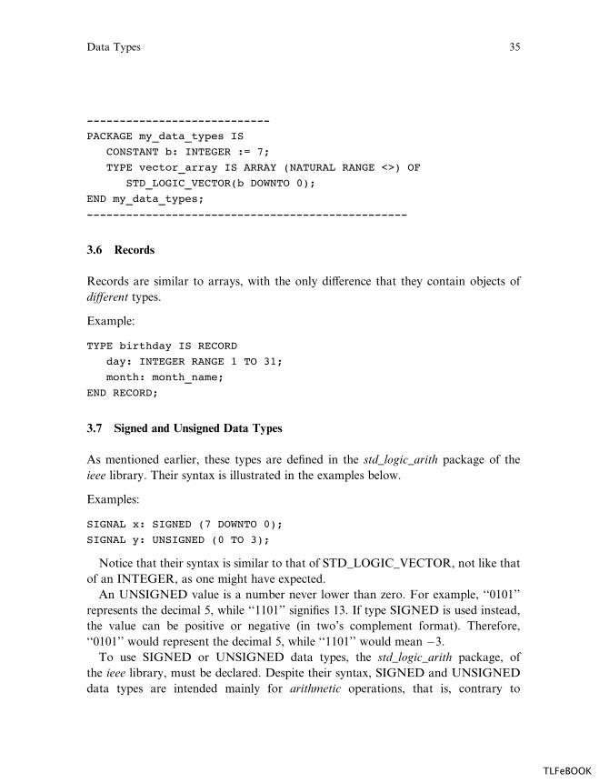
3.6 Records 35
3.7 Signed and Unsigned Data Types 35
3.8 Data Conversion 37
3.9 Summary 38
3.10 Additional Examples 38
3.11 Problems 43
4 Operators and Attributes 47
4.1 Operators 47
4.2 Attributes 50
4.3 User-Defined Attributes 52
4.4 Operator Overloading 53
TLFeBOOK

4.5 GENERIC 54
4.6 Examples 55
4.7 Summary 60
4.8 Problems 61
5 Concurrent Code 65
5.1 Concurrent versus Sequential 65
5.2 Using Operators 67
5.3 WHEN (Simple and Selected) 69
5.4 GENERATE 78
5.5 BLOCK 81
5.6 Problems 84
6 Sequential Code 91
6.1 PROCESS 91
6.2 Signals and Variables 93
6.3 IF 94
6.4 WAIT 97
6.5 CASE 100
6.6 LOOP 105
6.7 CASE versus IF 112
6.8 CASE versus WHEN 113
6.9 Bad Clocking 114
6.10 Using Sequential Code to Design Combinational Circuits 118
6.11 Problems 121
7 Signals and Variables 129
7.1 CONSTANT 129
7.2 SIGNAL 130
7.3 VARIABLE 131
7.4 SIGNAL versus VARIABLE 133
7.5 Number of Registers 140
7.6 Problems 151
8 State Machines 159
8.1 Introduction 159
8.2 Design Style #1 160
8.3 Design Style #2 (Stored Output) 168
viii Contents
TLFeBOOK
8.4 Encoding Style: From Binary to OneHot 181
8.5 Problems 183
9 Additional Circuit Designs 187
9.1 Barrel Shifter 187
9.2 Signed and Unsigned Comparators 191
9.3 Carry Ripple and Carry Look Ahead Adders 194
9.4 Fixed-Point Division 198
9.5 Vending-Machine Controller 202
9.6 Serial Data Receiver 208
9.7 Parallel-to-Serial Converter 211
9.8 Playing with a Seven-Segment Display 212
9.9 Signal Generators 217
9.10 Memory Design 220
9.11 Problems 225
II SYSTEM DESIGN 231
10 Packages and Components 233
10.1 Introduction 233
10.2 PACKAGE 234
10.3 COMPONENT 236
10.4 PORT MAP 244
10.5 GENERIC MAP 244
10.6 Problems 251
11 Functions and Procedures 253
11.1 FUNCTION 253
11.2 Function Location 256
11.3 PROCEDURE 265
11.4 Procedure Location 266
11.5 FUNCTION versus PROCEDURE Summary 270
11.6 ASSERT 270
11.7 Problems 271
12 Additional System Designs 275
12.1 Serial-Parallel Multiplier 275
12.2 Parallel Multiplier 279
Contents ix
TLFeBOOK
12.3 Multiply-Accumulate Circuits 285
12.4 Digital Filters 289
12.5 Neural Networks 294
12.6 Problems 301
Appendix A: Programmable Logic Devices 305
Appendix B: Xilinx ISEBModelSim Tutorial 317
Appendix C: Altera MaxPlus IIBAdvanced Synthesis Software
Tutorial 329
Appendix D: Altera Quartus II Tutorial 343
Appendix E: VHDL Reserved Words 355
Bibliography 357
Index 359
x Contents
TLFeBOOK
Preface
Structure of the Book
The book is divided into two parts: Circuit Design and System Design. The first part
deals with everything that goes directly inside the main code, while the second deals
with units that might be located in a library (for code sharing, reuse, and partitioning).
In summary, in Part I we study the entire background and coding techniques of
VHDL, which includes the following:
� Code structure: libraries, entity, architecture (chapter 2)
� Data types (chapter 3)
� Operators and attributes (chapter 4)
� Concurrent statements and concurrent code (chapter 5)
� Sequential statements and sequential code (chapter 6)
� Objects: signals, variables, constants (chapter 7)
� Design of finite state machines (chapter 8)
� And, finally, additional circuit designs are presented (chapter 9).
Then, in Part II we simply add new building blocks, which are intended mainly for
library allocation, to the material already presented. The structure of Part II is the
following:
� Packages and components (chapter 10)
� Functions and procedures (chapter 11)
� Finally, additional system designs are presented (chapter 12).
Distinguishing Features
The main distinguishing features of the book are the following:
� It teaches in detail all indispensable features of VHDL synthesis in a concise
format.
� The sequence is well established. For example, a clear distinction is made between
what is at the circuit level (Part I) versus what is at the system level (Part II). The
foundations of VHDL are studied in chapters 1 to 4, fundamental coding in chapters 5
to 9, and finally system coding in chapters 10 to 12.
� Each chapter is organized in such a way to collect together related information as
closely as possible. For instance, concurrent code is treated collectively in one chap-
TLFeBOOK
ter, while sequential code is treated in another; data types are discussed in one chap-
ter, while operators and attributes are in another; what is at the circuit level is seen in
one part of the book, while what is at the system level is in another.
� While books on VHDL give limited emphasis to digital design concepts, and books
on digital design discuss VHDL only briefly, the present work completely integrates
them. It is indeed a design-oriented approach.
� To achieve the above-mentioned integration between VHDL and digital design, the
following steps are taken:
� a large number of complete design examples (rather than sketchy or partial
solutions) are presented;
� illustrative top-level circuit diagrams are always shown;
� fundamental design concepts are reviewed;
� the solutions are explained and commented;
� the circuits are always physically implemented (using programmable logic devices);
� simulation results are always included, along with analysis and comments;
� finally, appendices on programmable devices and synthesis tools are also included.
Audience
The book is intended as a text for any of the following EE/CS courses:
� VHDL
� Automated Digital Design
� Programmable Logic Devices
� Digital Design (basic or advanced)
It is also a supporting text for in-house courses in any of the areas listed above,
particularly for vendor-provided courses on VHDL and/or programmable logic
devices.
Acknowledgments
To the anonymous reviewers for their invaluable comments and suggestions. Special
thanks also to Ricardo P. Jasinski and Bruno U. Pedroni for their reviews and
comments.
xii Preface
TLFeBOOK

I CIRCUIT DESIGN
TLFeBOOK

TLFeBOOK
1 Introduction
1.1 About VHDL
VHDL is a hardware description language. It describes the behavior of an electronic
circuit or system, from which the physical circuit or system can then be attained
(implemented).
VHDL stands for VHSIC Hardware Description Language. VHSIC is itself an
abbreviation for Very High Speed Integrated Circuits, an initiative funded by the
United States Department of Defense in the 1980s that led to the creation of VHDL.
Its first version was VHDL 87, later upgraded to the so-called VHDL 93. VHDL
was the original and first hardware description language to be standardized by the
Institute of Electrical and Electronics Engineers, through the IEEE 1076 standard.
An additional standard, the IEEE 1164, was later added to introduce a multi-valued
logic system.
VHDL is intended for circuit synthesis as well as circuit simulation. However,
though VHDL is fully simulatable, not all constructs are synthesizable. We will give
emphasis to those that are.
A fundamental motivation to use VHDL (or its competitor, Verilog) is that
VHDL is a standard, technology/vendor independent language, and is therefore
portable and reusable. The two main immediate applications of VHDL are in the
field of Programmable Logic Devices (including CPLDs—Complex Programmable
Logic Devices and FPGAs—Field Programmable Gate Arrays) and in the field of
ASICs (Application Specific Integrated Circuits). Once the VHDL code has been
written, it can be used either to implement the circuit in a programmable device
(from Altera, Xilinx, Atmel, etc.) or can be submitted to a foundry for fabrication
of an ASIC chip. Currently, many complex commercial chips (microcontrollers, for
example) are designed using such an approach.
A final note regarding VHDL is that, contrary to regular computer programs
which are sequential, its statements are inherently concurrent (parallel). For that
reason, VHDL is usually referred to as a code rather than a program. In VHDL,
only statements placed inside a PROCESS, FUNCTION, or PROCEDURE are
executed sequentially.
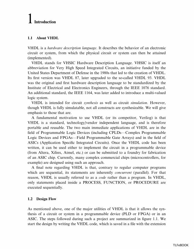
1.2 Design Flow
As mentioned above, one of the major utilities of VHDL is that it allows the syn-
thesis of a circuit or system in a programmable device (PLD or FPGA) or in an
ASIC. The steps followed during such a project are summarized in figure 1.1. We
start the design by writing the VHDL code, which is saved in a file with the extension
TLFeBOOK
.vhd and the same name as its ENTITY’s name. The first step in the synthesis pro-
cess is compilation. Compilation is the conversion of the high-level VHDL language,
which describes the circuit at the Register Transfer Level (RTL), into a netlist at the
gate level. The second step is optimization, which is performed on the gate-level net-
list for speed or for area. At this stage, the design can be simulated. Finally, a place-
and-route (fitter) software will generate the physical layout for a PLD/FPGA chip or
will generate the masks for an ASIC.
1.3 EDA Tools
There are several EDA (Electronic Design Automation) tools available for circuit
synthesis, implementation, and simulation using VHDL. Some tools (place and
route, for example) are o¤ered as part of a vendor’s design suite (e.g., Altera’s
Quartus II, which allows the synthesis of VHDL code onto Altera’s CPLD/FPGA
chips, or Xilinx’s ISE suite, for Xilinx’s CPLD/FPGA chips). Other tools (synthe-
Place & Route
Compilation
Optimization
Simulation
Simulation
VHDL entry(RTL level)
Netlist(Gate level)
Synthesis
Optimized netlist(Gate level)
Physicaldevice
Figure 1.1Summary of VHDL design flow.
4 Chapter 1
TLFeBOOK

sizers, for example), besides being o¤ered as part of the design suites, can also be
provided by specialized EDA companies (Mentor Graphics, Synopsis, Synplicity,
etc.). Examples of the latter group are Leonardo Spectrum (a synthesizer from
Mentor Graphics), Synplify (a synthesizer from Synplicity), and ModelSim (a simu-
lator from Model Technology, a Mentor Graphics company).
The designs presented in the book were synthesized onto CPLD/FPGA devices
(appendix A) either from Altera or Xilinx. The tools used were either ISE combined
with ModelSim (for Xilinx chips—appendix B), MaxPlus II combined with Ad-
vanced Synthesis Software (for Altera CPLDs—appendix C), or Quartus II (also
for Altera devices—appendix D). Leonardo Spectrum was also used occasionally.
Although di¤erent EDA tools were used to implement and test the examples
presented in the book (see list of tools above), we decided to standardize the visual
presentation of all simulation graphs. Due to its clean appearance, the waveform
editor of MaxPlus II (appendix C) was employed. However, newer simulators, like
ISEþModelSim (appendix B) and Quartus II (appendix D), o¤er a much broader
set of features, which allow, for example, a more refined timing analysis. For that
reason, those tools were adopted when examining the fine details of each design.
1.4 Translation of VHDL Code into a Circuit
A full-adder unit is depicted in figure 1.2. In it, a and b represent the input bits to be
added, cin is the carry-in bit, s is the sum bit, and cout the carry-out bit. As shown in
the truth table, s must be high whenever the number of inputs that are high is odd,
while cout must be high when two or more inputs are high.
A VHDL code for the full adder of figure 1.2 is shown in figure 1.3. As can be
seen, it consists of an ENTITY, which is a description of the pins (PORTS) of the
FullAdder
a
b
cin
s
cout
a b cin s cout0 0 00 1 01 0 01 1 0
0 01 01 00 1
0 0 10 1 11 0 11 1 1
1 00 10 11 1
Figure 1.2Full-adder diagram and truth table.
Introduction 5
TLFeBOOK
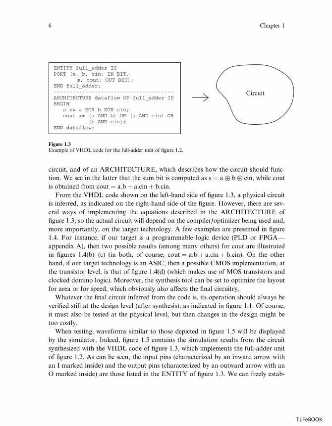
circuit, and of an ARCHITECTURE, which describes how the circuit should func-
tion. We see in the latter that the sum bit is computed as s ¼ aaba cin, while cout
is obtained from cout ¼ a.bþ a.cinþ b.cin.
From the VHDL code shown on the left-hand side of figure 1.3, a physical circuit
is inferred, as indicated on the right-hand side of the figure. However, there are sev-
eral ways of implementing the equations described in the ARCHITECTURE of
figure 1.3, so the actual circuit will depend on the compiler/optimizer being used and,
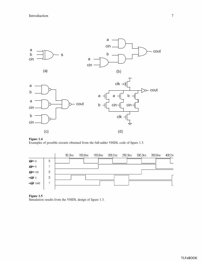
more importantly, on the target technology. A few examples are presented in figure
1.4. For instance, if our target is a programmable logic device (PLD or FPGA—
appendix A), then two possible results (among many others) for cout are illustrated
in figures 1.4(b)–(c) (in both, of course, cout ¼ a.bþ a.cinþ b.cin). On the other
hand, if our target technology is an ASIC, then a possible CMOS implementation, at
the transistor level, is that of figure 1.4(d) (which makes use of MOS transistors and
clocked domino logic). Moreover, the synthesis tool can be set to optimize the layout
for area or for speed, which obviously also a¤ects the final circuitry.
Whatever the final circuit inferred from the code is, its operation should always be
verified still at the design level (after synthesis), as indicated in figure 1.1. Of course,
it must also be tested at the physical level, but then changes in the design might be
too costly.
When testing, waveforms similar to those depicted in figure 1.5 will be displayed
by the simulator. Indeed, figure 1.5 contains the simulation results from the circuit
synthesized with the VHDL code of figure 1.3, which implements the full-adder unit
of figure 1.2. As can be seen, the input pins (characterized by an inward arrow with
an I marked inside) and the output pins (characterized by an outward arrow with an
O marked inside) are those listed in the ENTITY of figure 1.3. We can freely estab-
ENTITY full_adder ISPORT (a, b, cin: IN BIT;
s, cout: OUT BIT);END full_adder;--------------------------------------ARCHITECTURE dataflow OF full_adder ISBEGIN
s <= a XOR b XOR cin;cout <= (a AND b) OR (a AND cin) OR (b AND cin);
END dataflow;
Circuit
Figure 1.3Example of VHDL code for the full-adder unit of figure 1.2.
6 Chapter 1
TLFeBOOK
abcin
s
a
b
a
cin
b
cin
cout
a
cin
b
a
cin
cout
clk
a
b
a
cin
b
cin
cout
clk
(a) (b)
(c) (d)
Figure 1.4Examples of possible circuits obtained from the full-adder VHDL code of figure 1.3.
Figure 1.5Simulation results from the VHDL design of figure 1.3.
Introduction 7
TLFeBOOK

lish the values of the input signals (a, b, and cin in this case), and the simulator will
compute and plot the output signals (s and cout). As can be observed in figure 1.5,
the outputs do behave as expected.
1.5 Design Examples
As mentioned in the preface, the book is indeed a design-oriented approach to the
task of teaching VHDL. The integration between VHDL and Digital Design is
achieved through a long series of well-detailed design examples. A summary of the
complete designs presented in the book is shown below.
� Adders (examples 3.3 and 6.8 and section 9.3)
� ALU (examples 5.5 and 6.10)
� Barrel shifters and vector shifters (examples 5.6 and 6.9 and section 9.1)
� Comparators (section 9.2)
� Controller, tra‰c light (example 8.5)
� Controller, vending machine (section 9.5)
� Count ones (examples 7.1 and 7.2)
� Counters (examples 6.2, 6.5, 6.7, 7.7, and 8.1)
� Decoder (example 4.1)
� Digital filters (section 12.4)
� Dividers, fixed point (section 9.4)
� Flip-flops and latches (examples 2.1, 5.7, 5.8, 6.1, 6.4, 6.6, 7.4, and 7.6)
� Encoder (example 5.4)
� Frequency divider (example 7.5)
� Function arith_shift (example 11.7)
� Function conv_integer (examples 11.2 and 11.5)
� Function multiplier (example 11.8)
� Function ‘‘þ’’ overloaded (example 11.6)
� Function positive_edge (examples 11.1, 11.3, and 11.4)
� Leading zeros counter (example 6.10)
� Multiplexers (examples 5.1, 5.2, and 7.3)
8 Chapter 1
TLFeBOOK
� Multipliers (example 11.8 and sections 12.1 and 12.2)
� MAC circuit (section 12.3)
� Neural networks (section 12.5)
� Parallel-to-serial converter (section 9.7)
� Parity detector (example 4.2)
� Parity generator (example 4.3)
� Playing with SSD (section 9.8)
� Procedure min_max (examples 11.9 and 11.10)
� RAM (example 6.11 and section 9.10)
� ROM (section 9.10)
� Serial data receiver (section 9.6)
� Shift registers (examples 6.3, 7.8, and 7.9)
� Signal generators (example 8.6 and section 9.9)
� String detector (example 8.4)
� Tri-state bu¤er/bus (example 5.3)
Moreover, several additional designs and experimental verifications are also pro-
posed as exercises:
� Adders and subtractors (problems 3.5, 5.4, 5.5, 6.14, 6.16, 10.2, and 10.3)
� Arithmetic-logic units (problems 6.13 and 10.1)
� Barrel and vector shifters (problems 5.7, 6.12, 9.1, and 12.2)
� Binary-to-Gray code converter (problem 5.6)
� Comparators (problems 5.8 and 6.15)
� Count ones (problem 6.9)
� Counters (problems 7.5 and 11.6)
� Data delay circuit (problem 7.2)
� Decoders (problems 4.4 and 7.6)
� DFFs (problems 6.17, 7.3, 7.4, and 7.7)
� Digital FIR filter (problem 12.4)
� Dividers (problems 5.3 and 9.2)
� Event counter (problem 6.1)
Introduction 9
TLFeBOOK
� Finite-state machine (problem 8.1)
� Frequency divider, generic (problem 6.4)
� Frequency multiplier (problem 6.5)
� Function conv_std_logic_vector (problem 11.1)
� Function ‘‘not’’ overloaded for integers (problem 11.2)
� Function shift for integers (problem 11.4)
� Function shift for std_logic_vector (problem 11.3)
� Function BCD-SSD converter (problem 11.6)
� Function ‘‘þ’’ overloaded for std_logic_vector (problem 11.8)
� Intensity encoder (problem 6.10)
� Keypad debouncer/encoder (problem 8.4)
� Multiplexers (problems 2.1, 5.1, and 6.11)
� Multipliers (problems 5.3, 11.5, and 12.1)
� Multiply-accumulate circuit (problem 12.3)
� Neural network (problem 12.5)
� Parity detector (problem 6.8)
� Playing with a seven-segment display (problem 9.6)
� Priority encoder (problems 5.2 and 6.3)
� Procedure statistics (problem 11.7)
� Random number generator plus SSD (problem 9.8)
� ROM (problem 3.4)
� Serial data receiver (problem 9.4)
� Serial data transmitter (problem 9.5)
� Shift register (problem 6.2)
� Signal generators (problems 8.2, 8.3, 8.6, and 8.7)
� Speed monitor (problem 9.7)
� Stop watch (problem 10.4)
� Timers (problems 6.6 and 6.7)
� Tra‰c-light controller (problem 8.5)
� Vending-machine controller (problem 9.3)
10 Chapter 1
TLFeBOOK
Additionally, four appendices on programmable logic devices and synthesis tools
are included:
� Appendix A: Programmable Logic Devices
� Appendix B: Xilinx ISEþModelSim Tutorial
� Appendix C: Altera MaxPlus IIþAdvanced Synthesis Software Tutorial
� Appendix D: Altera Quartus II Tutorial
Introduction 11
TLFeBOOK

TLFeBOOK
2 Code Structure
In this chapter, we describe the fundamental sections that comprise a piece of VHDL
code: LIBRARY declarations, ENTITY, and ARCHITECTURE.
2.1 Fundamental VHDL Units
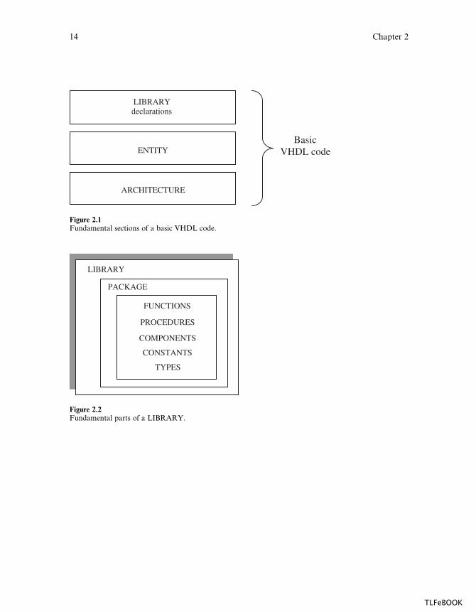
As depicted in figure 2.1, a standalone piece of VHDL code is composed of at least
three fundamental sections:
� LIBRARY declarations: Contains a list of all libraries to be used in the design. For
example: ieee, std, work, etc.
� ENTITY: Specifies the I/O pins of the circuit.
� ARCHITECTURE: Contains the VHDL code proper, which describes how the
circuit should behave (function).
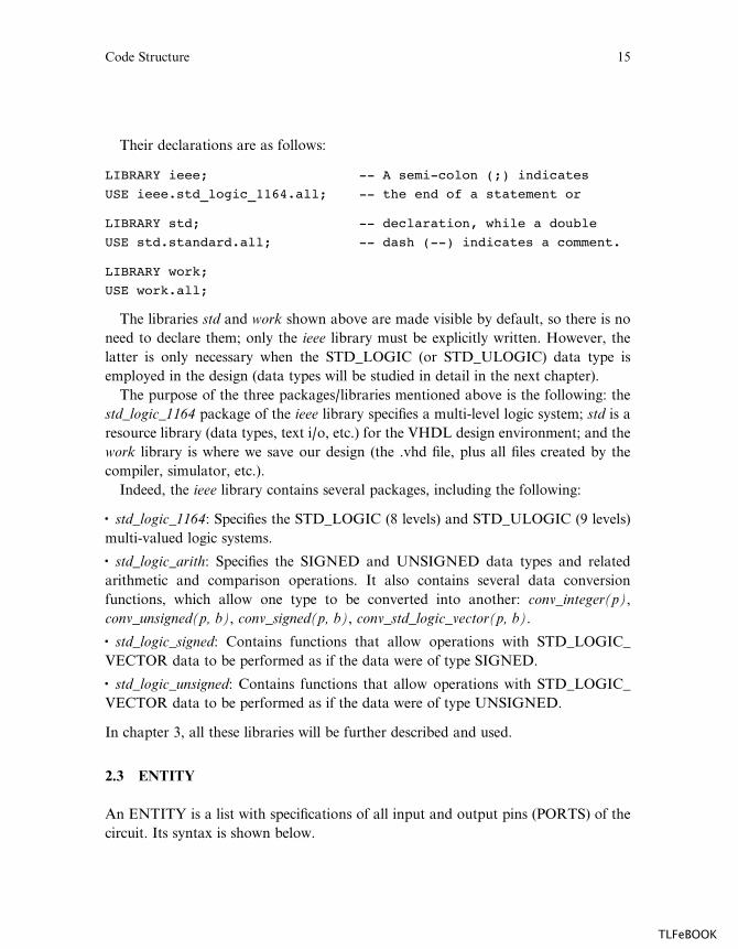
A LIBRARY is a collection of commonly used pieces of code. Placing such pieces
inside a library allows them to be reused or shared by other designs.
The typical structure of a library is illustrated in figure 2.2. The code is usually
written in the form of FUNCTIONS, PROCEDURES, or COMPONENTS, which
are placed inside PACKAGES, and then compiled into the destination library.
The fundamental units of VHDL (figure 2.1) will be studied in Part I of the book
(up to chapter 9), whereas the library-related sections (figure 2.2) will be seen in Part
II (chapters 10–12).
2.2 Library Declarations
To declare a LIBRARY (that is, to make it visible to the design) two lines of code
are needed, one containing the name of the library, and the other a use clause, as
shown in the syntax below.
LIBRARY library_name;USE library_name.package_name.package_parts;
At least three packages, from three di¤erent libraries, are usually needed in a
design:
� ieee.std_logic_1164 (from the ieee library),
� standard (from the std library), and
� work (work library).
TLFeBOOK
LIBRARYdeclarations
ENTITY
ARCHITECTURE
BasicVHDL code
Figure 2.1Fundamental sections of a basic VHDL code.
LIBRARY
PACKAGE
FUNCTIONS
COMPONENTS
PROCEDURES
CONSTANTS
TYPES
Figure 2.2Fundamental parts of a LIBRARY.
14 Chapter 2
TLFeBOOK
Their declarations are as follows:
LIBRARY ieee; -- A semi-colon (;) indicates
USE ieee.std_logic_1164.all; -- the end of a statement or
LIBRARY std; -- declaration, while a double
USE std.standard.all; -- dash (--) indicates a comment.
LIBRARY work;
USE work.all;
The libraries std and work shown above are made visible by default, so there is no
need to declare them; only the ieee library must be explicitly written. However, the
latter is only necessary when the STD_LOGIC (or STD_ULOGIC) data type is
employed in the design (data types will be studied in detail in the next chapter).
The purpose of the three packages/libraries mentioned above is the following: the
std_logic_1164 package of the ieee library specifies a multi-level logic system; std is a
resource library (data types, text i/o, etc.) for the VHDL design environment; and the
work library is where we save our design (the .vhd file, plus all files created by the
compiler, simulator, etc.).
Indeed, the ieee library contains several packages, including the following:
� std_logic_1164: Specifies the STD_LOGIC (8 levels) and STD_ULOGIC (9 levels)
multi-valued logic systems.
� std_logic_arith: Specifies the SIGNED and UNSIGNED data types and related
arithmetic and comparison operations. It also contains several data conversion
functions, which allow one type to be converted into another: conv_integer(p),
conv_unsigned(p, b), conv_signed(p, b), conv_std_logic_vector(p, b).
� std_logic_signed: Contains functions that allow operations with STD_LOGIC_
VECTOR data to be performed as if the data were of type SIGNED.
� std_logic_unsigned: Contains functions that allow operations with STD_LOGIC_
VECTOR data to be performed as if the data were of type UNSIGNED.
In chapter 3, all these libraries will be further described and used.
2.3 ENTITY
An ENTITY is a list with specifications of all input and output pins (PORTS) of the
circuit. Its syntax is shown below.
Code Structure 15
TLFeBOOK

ENTITY entity_name ISPORT (
port_name : signal_mode signal_type;port_name : signal_mode signal_type;...);
END entity_name;
The mode of the signal can be IN, OUT, INOUT, or BUFFER. As illustrated in
figure 2.3, IN and OUT are truly unidirectional pins, while INOUT is bidirectional.
BUFFER, on the other hand, is employed when the output signal must be used
(read) internally.
The type of the signal can be BIT, STD_LOGIC, INTEGER, etc. Data types will
be discussed in detail in chapter 3.
Finally, the name of the entity can be basically any name, except VHDL reserved
words (VHDL reserved words are listed in appendix E).
Example: Let us consider the NAND gate of figure 2.4. Its ENTITY can be specified
as:
ENTITY nand_gate IS
PORT (a, b : IN BIT;
x : OUT BIT);
END nand_gate;
OUT
INOUT
BUFFER
IN Circuit
Figure 2.3Signal modes.
a
bx
Figure 2.4NAND gate.
16 Chapter 2
TLFeBOOK
The meaning of the ENTITY above is the following: the circuit has three I/O pins,
being two inputs (a and b, mode IN) and one output (x, mode OUT). All three signals
are of type BIT. The name chosen for the entity was nand_gate.
2.4 ARCHITECTURE
The ARCHITECTURE is a description of how the circuit should behave (function).
Its syntax is the following:
ARCHITECTURE architecture_name OF entity_name IS[declarations]
BEGIN(code)
END architecture_name;
As shown above, an architecture has two parts: a declarative part (optional), where
signals and constants (among others) are declared, and the code part (from BEGIN
down). Like in the case of an entity, the name of an architecture can be basically any
name (except VHDL reserved words), including the same name as the entity’s.
Example: Let us consider the NAND gate of figure 2.4 once again.
ARCHITECTURE myarch OF nand_gate IS
BEGIN
x <= a NAND b;
END myarch;
The meaning of the ARCHITECTURE above is the following: the circuit must
perform the NAND operation between the two input signals (a, b) and assign (‘‘<¼’’)
the result to the output pin (x). The name chosen for this architecture was myarch.
In this example, there is no declarative part, and the code contains just a single
assignment.
2.5 Introductory Examples
In this section, we will present two initial examples of VHDL code. Though we have
not yet studied the constructs that appear in the examples, they will help illustrate
fundamental aspects regarding the overall code structure. Each example is followed
by explanatory comments and simulation results.
Code Structure 17
TLFeBOOK
Example 2.1: DFF with Asynchronous Reset
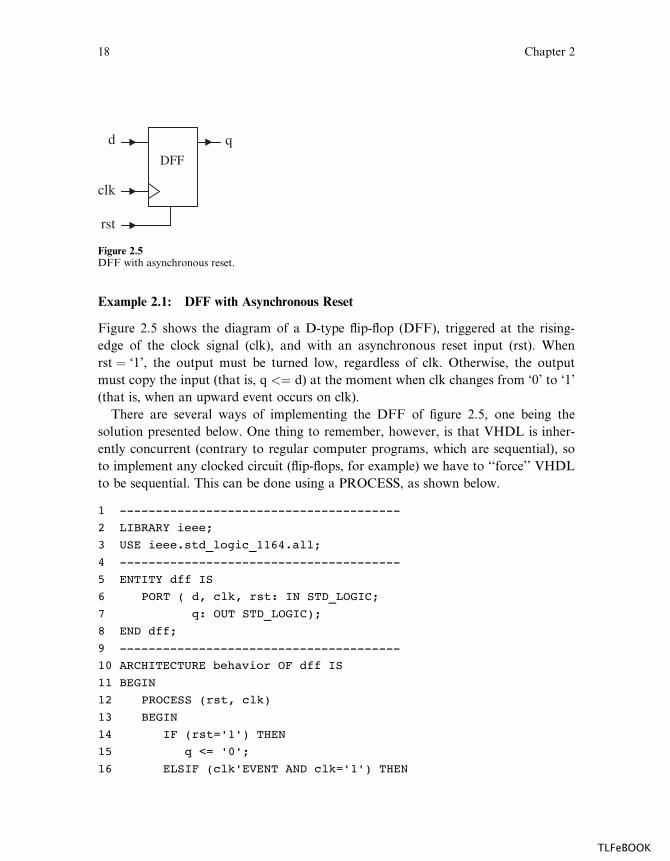
Figure 2.5 shows the diagram of a D-type flip-flop (DFF), triggered at the rising-
edge of the clock signal (clk), and with an asynchronous reset input (rst). When
rst ¼ ‘1’, the output must be turned low, regardless of clk. Otherwise, the output
must copy the input (that is, q <¼ d) at the moment when clk changes from ‘0’ to ‘1’
(that is, when an upward event occurs on clk).
There are several ways of implementing the DFF of figure 2.5, one being the
solution presented below. One thing to remember, however, is that VHDL is inher-
ently concurrent (contrary to regular computer programs, which are sequential), so
to implement any clocked circuit (flip-flops, for example) we have to ‘‘force’’ VHDL
to be sequential. This can be done using a PROCESS, as shown below.
1 ---------------------------------------
2 LIBRARY ieee;
3 USE ieee.std_logic_1164.all;
4 ---------------------------------------
5 ENTITY dff IS
6 PORT ( d, clk, rst: IN STD_LOGIC;
7 q: OUT STD_LOGIC);
8 END dff;
9 ---------------------------------------
10 ARCHITECTURE behavior OF dff IS
11 BEGIN
12 PROCESS (rst, clk)
13 BEGIN
14 IF (rst='1') THEN
15 q <= '0';
16 ELSIF (clk'EVENT AND clk='1') THEN
d
clk
rst
q
DFF
Figure 2.5DFF with asynchronous reset.
18 Chapter 2
TLFeBOOK
17 q <= d;
18 END IF;
19 END PROCESS;
20 END behavior;
21 ---------------------------------------
Comments:
Lines 2–3: Library declaration (library name and library use clause). Recall that the
other two indispensable libraries (std and work) are made visible by default.
Lines 5–8: Entity d¤.
Lines 10–20: Architecture behavior.
Line 6: Input ports (input mode can only be IN). In this example, all input signals are
of type STD_LOGIC.
Line 7: Output port (output mode can be OUT, INOUT, or BUFFER). Here, the
output is also of type STD_LOGIC.
Lines 11–19: Code part of the architecture (from word BEGIN on).
Lines 12–19: A PROCESS (inside it the code is executed sequentially).
Line 12: The PROCESS is executed every time a signal declared in its sensitivity list
changes. In this example, every time rst or clk changes the PROCESS is run.
Lines 14–15: Every time rst goes to ‘1’ the output is reset, regardless of clk (asyn-
chronous reset).
Lines 16–17: If rst is not active, plus clk has changed (an EVENT occurred on clk),
plus such event was a rising edge (clk ¼ ‘1’), then the input signal (d) is stored in the
flip-flop (q <¼ d).
Lines 15 and 17: The ‘‘<¼’’ operator is used to assign a value to a SIGNAL. In
contrast, ‘‘:¼’’ would be used for a VARIABLE. All ports in an entity are signals by
default.
Lines 1, 4, 9, and 21: Commented out (recall that ‘‘- -’’ indicates a comment). Used
only to better organize the design.
Note: VHDL is not case sensitive.
Simulation results:
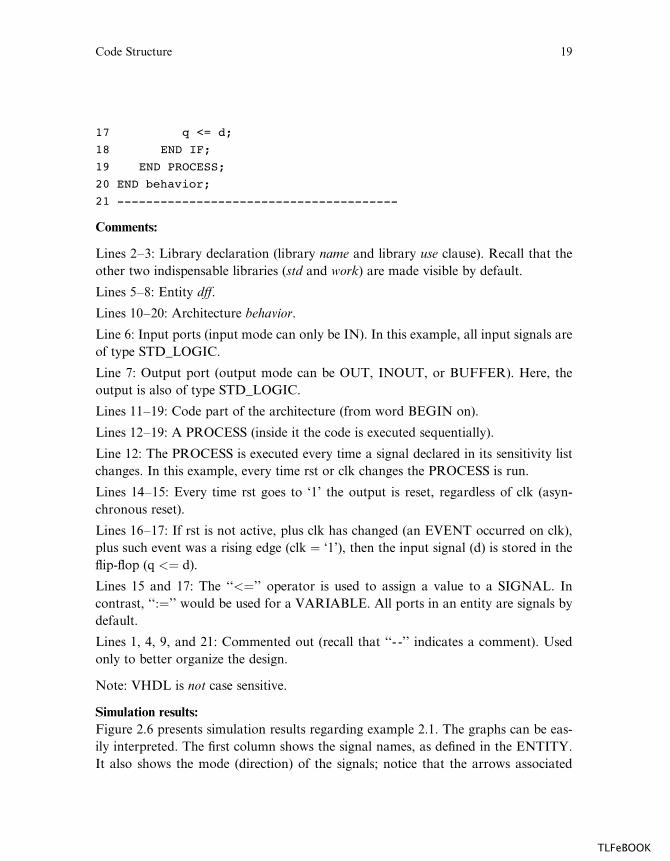
Figure 2.6 presents simulation results regarding example 2.1. The graphs can be eas-
ily interpreted. The first column shows the signal names, as defined in the ENTITY.
It also shows the mode (direction) of the signals; notice that the arrows associated
Code Structure 19
TLFeBOOK
with rst, d, and clk are inward, and contain the letter I (input) inside, while that of q
is outward and has an O (output) marked inside. The second column has the value of
each signal in the position where the vertical cursor is placed. In the present case, the
cursor is at 0ns, where the signals have value 1, 0, 0, 0, respectively. In this example,
the values are simply ‘0’ or ‘1’, but when vectors are used, the values can be shown in
binary, decimal, or hexadecimal form. The third column shows the simulation
proper. The input signals (rst, d, clk) can be chosen freely, and the simulator will
determine the corresponding output (q). Comparing the results of figure 2.6 with
those expected from the circuit shown previously, we notice that it works properly.
As mentioned earlier, the designs presented in the book were synthesized onto CPLD/
FPGA devices (appendix A), either from Altera or Xilinx. The tools used were either
ISE combined with ModelSim (for Xilinx chips—appendix B), or MaxPlus II com-
bined with Advanced Synthesis Software (for Altera CPLDs—appendix C), or
Quartus II (also for Altera devices—appendix D). Leonardo Spectrum (from Mentor
Graphics) was also used occasionally.
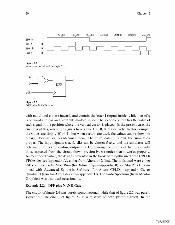
Example 2.2: DFF plus NAND Gate
The circuit of figure 2.4 was purely combinational, while that of figure 2.5 was purely
sequential. The circuit of figure 2.7 is a mixture of both (without reset). In the
Figure 2.6Simulation results of example 2.1.
a
b
clk
qDFF
Figure 2.7DFF plus NAND gate.
20 Chapter 2
TLFeBOOK
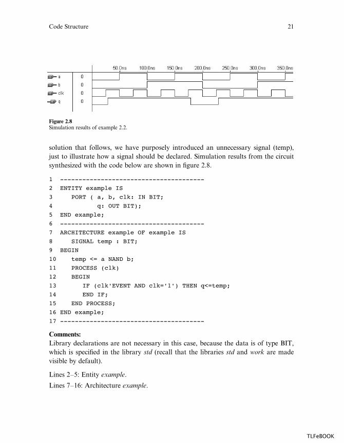
solution that follows, we have purposely introduced an unnecessary signal (temp),
just to illustrate how a signal should be declared. Simulation results from the circuit
synthesized with the code below are shown in figure 2.8.
1 ---------------------------------------
2 ENTITY example IS
3 PORT ( a, b, clk: IN BIT;
4 q: OUT BIT);
5 END example;
6 ---------------------------------------
7 ARCHITECTURE example OF example IS
8 SIGNAL temp : BIT;
9 BEGIN
10 temp <= a NAND b;
11 PROCESS (clk)
12 BEGIN
13 IF (clk'EVENT AND clk='1') THEN q<=temp;
14 END IF;
15 END PROCESS;
16 END example;
17 ---------------------------------------
Comments:
Library declarations are not necessary in this case, because the data is of type BIT,
which is specified in the library std (recall that the libraries std and work are made
visible by default).
Lines 2–5: Entity example.
Lines 7–16: Architecture example.
Figure 2.8Simulation results of example 2.2.
Code Structure 21
TLFeBOOK
Line 3: Input ports (all of type BIT).
Line 4: Output port (also of type BIT).
Line 8: Declarative part of the architecture (optional). The signal temp, of type BIT,
was declared. Notice that there is no mode declaration (mode is only used in entities).
Lines 9–15: Code part of the architecture (from word BEGIN on).
Lines 11–15: A PROCESS (sequential statements executed every time the signal clk
changes).
Lines 10 and 11–15: Though within a process the execution is sequential, the process,
as a whole, is concurrent with the other (external) statements; thus line 10 is executed
concurrently with the block 11–15.
Line 10: Logical NAND operation. Result is assigned to signal temp.
Lines 13–14: IF statement. At the rising edge of clk the value of temp is assigned to q.
Lines 10 and 13: The ‘‘<¼’’ operator is used to assign a value to a SIGNAL. In
contrast, ‘‘:¼’’ would be used for a VARIABLE.
Lines 8 and 10: Can be eliminated, changing ‘‘q <¼ a NAND b’’ in line 13.
Lines 1, 6, and 17: Commented out. Used only to better organize the design.
2.6 Problems
Problem 2.1: Multiplexer
The top-level diagram of a multiplexer is shown in figure P2.1. According to the
truth table, the output should be equal to one of the inputs if sel ¼ ‘‘01’’ (c ¼ a) or
sel ¼ ‘‘10’’ (c ¼ b), but it should be ‘0’ or Z (high impedance) if sel ¼ ‘‘00’’ or
sel ¼ ‘‘11’’, respectively.
sel00011011
0abZ
sel (1:0)
a (7:0)
b (7:0)
c (7:0)MUX
c
Figure P2.1
22 Chapter 2
TLFeBOOK
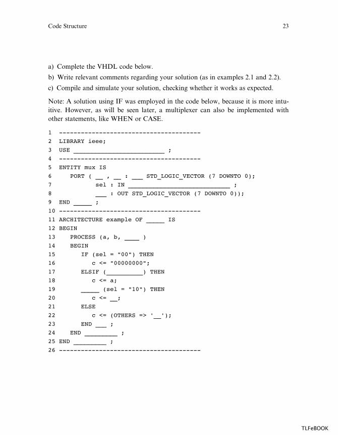
a) Complete the VHDL code below.
b) Write relevant comments regarding your solution (as in examples 2.1 and 2.2).
c) Compile and simulate your solution, checking whether it works as expected.
Note: A solution using IF was employed in the code below, because it is more intu-
itive. However, as will be seen later, a multiplexer can also be implemented with
other statements, like WHEN or CASE.
1 ---------------------------------------
2 LIBRARY ieee;
3 USE _________________________ ;
4 ---------------------------------------
5 ENTITY mux IS
6 PORT ( __ , __ : ___ STD_LOGIC_VECTOR (7 DOWNTO 0);
7 sel : IN ____________________________ ;
8 ___ : OUT STD_LOGIC_VECTOR (7 DOWNTO 0));
9 END _____ ;
10 ---------------------------------------
11 ARCHITECTURE example OF _____ IS
12 BEGIN
13 PROCESS (a, b, ____ )
14 BEGIN
15 IF (sel = "00") THEN
16 c <= "00000000";
17 ELSIF (__________) THEN
18 c <= a;
19 _____ (sel = "10") THEN
20 c <= __;
21 ELSE
22 c <= (OTHERS => '__');
23 END ___ ;
24 END _________ ;
25 END _________ ;
26 ---------------------------------------
Code Structure 23
TLFeBOOK

Problem 2.2: Logic Gates
a) Write a VHDL code for the circuit of figure P2.2. Notice that it is purely combi-
national, so a PROCESS is not necessary. Write an expression for d using only logi-
cal operators (AND, OR, NAND, NOT, etc.).
b) Synthesize and simulate your circuit. After assuring that it works properly, open
the report file and check the actual expression implemented by the compiler. Com-
pare it with your expression.
a
b
c
d
Figure P2.2
24 Chapter 2
TLFeBOOK
3 Data Types
In order to write VHDL code e‰ciently, it is essential to know what data types are
allowed, and how to specify and use them. In this chapter, all fundamental data
types are described, with special emphasis on those that are synthesizable. Discus-
sions on data compatibility and data conversion are also included.
3.1 Pre-Defined Data Types
VHDL contains a series of pre-defined data types, specified through the IEEE 1076
and IEEE 1164 standards. More specifically, such data type definitions can be found
in the following packages / libraries:
� Package standard of library std: Defines BIT, BOOLEAN, INTEGER, and REAL
data types.
� Package std_logic_1164 of library ieee: Defines STD_LOGIC and STD_ULOGIC
data types.
� Package std_logic_arith of library ieee: Defines SIGNED and UNSIGNED
data types, plus several data conversion functions, like conv_integer(p),
conv_unsigned(p, b), conv_signed(p, b), and conv_std_logic_vector(p, b).
� Packages std_logic_signed and std_logic_unsigned of library ieee: Contain functions
that allow operations with STD_LOGIC_VECTOR data to be performed as if the
data were of type SIGNED or UNSIGNED, respectively.
All pre-defined data types (specified in the packages/libraries listed above) are
described below.
� BIT (and BIT_VECTOR): 2-level logic (‘0’, ‘1’).
Examples:
SIGNAL x: BIT;
-- x is declared as a one-digit signal of type BIT.
SIGNAL y: BIT_VECTOR (3 DOWNTO 0);
-- y is a 4-bit vector, with the leftmost bit being the MSB.
SIGNAL w: BIT_VECTOR (0 TO 7);
-- w is an 8-bit vector, with the rightmost bit being the MSB.
Based on the signals above, the following assignments would be legal (to assign a
value to a signal, the ‘‘<¼’’ operator must be used):
TLFeBOOK

x <= '1';
-- x is a single-bit signal (as specified above), whose value is
-- '1'. Notice that single quotes (' ') are used for a single bit.
y <= "0111";
-- y is a 4-bit signal (as specified above), whose value is "0111"
-- (MSB='0'). Notice that double quotes (" ") are used for
-- vectors.
w <= "01110001";
-- w is an 8-bit signal, whose value is "01110001" (MSB='1').
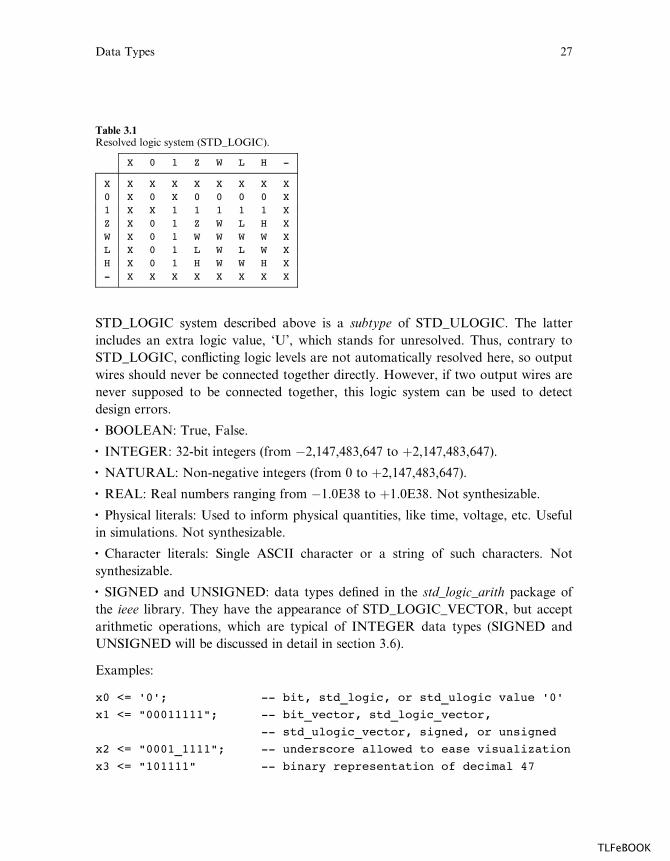
� STD_LOGIC (and STD_LOGIC_VECTOR): 8-valued logic system introduced in
the IEEE 1164 standard.
‘X’ Forcing Unknown (synthesizable unknown)
‘0’ Forcing Low (synthesizable logic ‘1’)
‘1’ Forcing High (synthesizable logic ‘0’)
‘Z’ High impedance (synthesizable tri-state bu¤er)
‘W’ Weak unknown
‘L’ Weak low
‘H’ Weak high
‘–’ Don’t care
Examples:
SIGNAL x: STD_LOGIC;
-- x is declared as a one-digit (scalar) signal of type STD_LOGIC.
SIGNAL y: STD_LOGIC_VECTOR (3 DOWNTO 0) := "0001";
-- y is declared as a 4-bit vector, with the leftmost bit being
-- the MSB. The initial value (optional) of y is "0001". Notice
-- that the ":=" operator is used to establish the initial value.
Most of the std_logic levels are intended for simulation only. However, ‘0’, ‘1’, and
‘Z’ are synthesizable with no restrictions. With respect to the ‘‘weak’’ values, they are
resolved in favor of the ‘‘forcing’’ values in multiply-driven nodes (see table 3.1).
Indeed, if any two std_logic signals are connected to the same node, then conflicting
logic levels are automatically resolved according to table 3.1.
� STD_ULOGIC (STD_ULOGIC_VECTOR): 9-level logic system introduced in
the IEEE 1164 standard (‘U’, ‘X’, ‘0’, ‘1’, ‘Z’, ‘W’, ‘L’, ‘H’, ‘–’). Indeed, the
26 Chapter 3
TLFeBOOK
STD_LOGIC system described above is a subtype of STD_ULOGIC. The latter
includes an extra logic value, ‘U’, which stands for unresolved. Thus, contrary to
STD_LOGIC, conflicting logic levels are not automatically resolved here, so output
wires should never be connected together directly. However, if two output wires are
never supposed to be connected together, this logic system can be used to detect
design errors.
� BOOLEAN: True, False.
� INTEGER: 32-bit integers (from �2,147,483,647 to þ2,147,483,647).
� NATURAL: Non-negative integers (from 0 to þ2,147,483,647).
� REAL: Real numbers ranging from �1.0E38 to þ1.0E38. Not synthesizable.
� Physical literals: Used to inform physical quantities, like time, voltage, etc. Useful
in simulations. Not synthesizable.
� Character literals: Single ASCII character or a string of such characters. Not
synthesizable.
� SIGNED and UNSIGNED: data types defined in the std_logic_arith package of
the ieee library. They have the appearance of STD_LOGIC_VECTOR, but accept
arithmetic operations, which are typical of INTEGER data types (SIGNED and
UNSIGNED will be discussed in detail in section 3.6).
Examples:
x0 <= '0'; -- bit, std_logic, or std_ulogic value '0'
x1 <= "00011111"; -- bit_vector, std_logic_vector,
-- std_ulogic_vector, signed, or unsigned
x2 <= "0001_1111"; -- underscore allowed to ease visualization
x3 <= "101111" -- binary representation of decimal 47
Table 3.1Resolved logic system (STD_LOGIC).
X 0 1 Z W L H -
X X X X X X X X X0 X 0 X 0 0 0 0 X1 X X 1 1 1 1 1 XZ X 0 1 Z W L H XW X 0 1 W W W W XL X 0 1 L W L W XH X 0 1 H W W H X- X X X X X X X X
Data Types 27
TLFeBOOK
x4 <= B"101111" -- binary representation of decimal 47
x5 <= O"57" -- octal representation of decimal 47
x6 <= X"2F" -- hexadecimal representation of decimal 47
n <= 1200; -- integer
m <= 1_200; -- integer, underscore allowed
IF ready THEN... -- Boolean, executed if ready=TRUE
y <= 1.2E-5; -- real, not synthesizable
q <= d after 10 ns; -- physical, not synthesizable
Example: Legal and illegal operations between data of di¤erent types.
SIGNAL a: BIT;
SIGNAL b: BIT_VECTOR(7 DOWNTO 0);
SIGNAL c: STD_LOGIC;
SIGNAL d: STD_LOGIC_VECTOR(7 DOWNTO 0);
SIGNAL e: INTEGER RANGE 0 TO 255;
...
a <= b(5); -- legal (same scalar type: BIT)
b(0) <= a; -- legal (same scalar type: BIT)
c <= d(5); -- legal (same scalar type: STD_LOGIC)
d(0) <= c; -- legal (same scalar type: STD_LOGIC)
a <= c; -- illegal (type mismatch: BIT x STD_LOGIC)
b <= d; -- illegal (type mismatch: BIT_VECTOR x
-- STD_LOGIC_VECTOR)
e <= b; -- illegal (type mismatch: INTEGER x BIT_VECTOR)
e <= d; -- illegal (type mismatch: INTEGER x
-- STD_LOGIC_VECTOR)
3.2 User-Defined Data Types
VHDL also allows the user to define his/her own data types. Two categories of user-
defined data types are shown below: integer and enumerated.
� User-defined integer types:
TYPE integer IS RANGE -2147483647 TO +2147483647;
-- This is indeed the pre-defined type INTEGER.
TYPE natural IS RANGE 0 TO +2147483647;
-- This is indeed the pre-defined type NATURAL.
28 Chapter 3
TLFeBOOK
TYPE my_integer IS RANGE -32 TO 32;
-- A user-defined subset of integers.
TYPE student_grade IS RANGE 0 TO 100;
-- A user-defined subset of integers or naturals.
� User-defined enumerated types:
TYPE bit IS ('0', '1');
-- This is indeed the pre-defined type BIT
TYPE my_logic IS ('0', '1', 'Z');
-- A user-defined subset of std_logic.
TYPE bit_vector IS ARRAY (NATURAL RANGE <>) OF BIT;
-- This is indeed the pre-defined type BIT_VECTOR.
-- RANGE <> is used to indicate that the range is unconstrained.
-- NATURAL RANGE <>, on the other hand, indicates that the only
-- restriction is that the range must fall within the NATURAL
-- range.
TYPE state IS (idle, forward, backward, stop);
-- An enumerated data type, typical of finite state machines.
TYPE color IS (red, green, blue, white);
-- Another enumerated data type.
The encoding of enumerated types is done sequentially and automatically (unless
specified otherwise by a user-defined attribute, as will be shown in chapter 4). For
example, for the type color above, two bits are necessary (there are four states), being
‘‘00’’ assigned to the first state (red), ‘‘01’’ to the second (green), ‘‘10’’ to the next
(blue), and finally ‘‘11’’ to the last state (white).
3.3 Subtypes
A SUBTYPE is a TYPE with a constraint. The main reason for using a subtype
rather than specifying a new type is that, though operations between data of di¤erent
types are not allowed, they are allowed between a subtype and its corresponding base
type.
Examples: The subtypes below were derived from the types presented in the previous
examples.
Data Types 29
TLFeBOOK
SUBTYPE natural IS INTEGER RANGE 0 TO INTEGER'HIGH;
-- As expected, NATURAL is a subtype (subset) of INTEGER.
SUBTYPE my_logic IS STD_LOGIC RANGE '0' TO 'Z';
-- Recall that STD_LOGIC=('X','0','1','Z','W','L','H','-').
-- Therefore, my_logic=('0','1','Z').
SUBTYPE my_color IS color RANGE red TO blue;
-- Since color=(red, green, blue, white), then
-- my_color=(red, green, blue).
SUBTYPE small_integer IS INTEGER RANGE -32 TO 32;
-- A subtype of INTEGER.
Example: Legal and illegal operations between types and subtypes.
SUBTYPE my_logic IS STD_LOGIC RANGE '0' TO '1';
SIGNAL a: BIT;
SIGNAL b: STD_LOGIC;
SIGNAL c: my_logic;
...
b <= a; -- illegal (type mismatch: BIT versus STD_LOGIC)
b <= c; -- legal (same "base" type: STD_LOGIC)
3.4 Arrays
Arrays are collections of objects of the same type. They can be one-dimensional
(1D), two-dimensional (2D), or one-dimensional-by-one-dimensional (1Dx1D). They
can also be of higher dimensions, but then they are generally not synthesizable.
Figure 3.1 illustrates the construction of data arrays. A single value (scalar) is
shown in (a), a vector (1D array) in (b), an array of vectors (1Dx1D array) in (c), and
an array of scalars (2D array) in (d).
Indeed, the pre-defined VHDL data types (seen in section 3.1) include only the
scalar (single bit) and vector (one-dimensional array of bits) categories. The pre-
defined synthesizable types in each of these categories are the following:
� Scalars: BIT, STD_LOGIC, STD_ULOGIC, and BOOLEAN.
� Vectors: BIT_VECTOR, STD_LOGIC_VECTOR, STD_ULOGIC_VECTOR,
INTEGER, SIGNED, and UNSIGNED.
30 Chapter 3
TLFeBOOK

As can be seen, there are no pre-defined 2D or 1Dx1D arrays, which, when nec-
essary, must be specified by the user. To do so, the new TYPE must first be defined,
then the new SIGNAL, VARIABLE, or CONSTANT can be declared using that
data type. The syntax below should be used.
To specify a new array type:
TYPE type_name IS ARRAY (specification) OF data_type;
To make use of the new array type:
SIGNAL signal_name: type_name [:= initial_value];
In the syntax above, a SIGNAL was declared. However, it could also be a CON-
STANT or a VARIABLE. Notice that the initial value is optional (for simulation
only).
Example: 1Dx1D array.
Say that we want to build an array containing four vectors, each of size eight bits.
This is then an 1Dx1D array (see figure 3.1). Let us call each vector by row, and the
complete array by matrix. Additionally, say that we want the leftmost bit of each
vector to be its MSB (most significant bit), and that we want the top row to be row 0.
Then the array implementation would be the following (notice that a signal, called x,
of type matrix, was declared as an example):
TYPE row IS ARRAY (7 DOWNTO 0) OF STD_LOGIC; -- 1D array
TYPE matrix IS ARRAY (0 TO 3) OF row; -- 1Dx1D array
SIGNAL x: matrix; -- 1Dx1D signal
(a) (b) (c) (d)
0 1 0 0 0
1 0 0 1 0
1 1 0 0 11 1 0 0 1
1 0 0 1 0
0 1 0 0 0
0 0 1 0 0 0
Figure 3.1Illustration of (a) scalar, (b) 1D, (c) 1Dx1D, and (d) 2D data arrays.
Data Types 31
TLFeBOOK
Example: Another 1Dx1D array.
Another way of constructing the 1Dx1D array above would be the following:
TYPE matrix IS ARRAY (0 TO 3) OF STD_LOGIC_VECTOR(7 DOWNTO 0);
From a data-compatibility point of view, the latter might be advantageous over
that in the previous example (see example 3.1).
Example: 2D array.
The array below is truly two-dimensional. Notice that its construction is not based
on vectors, but rather entirely on scalars.
TYPE matrix2D IS ARRAY (0 TO 3, 7 DOWNTO 0) OF STD_LOGIC;
-- 2D array
Example: Array initialization.
As shown in the syntax above, the initial value of a SIGNAL or VARIABLE is op-
tional. However, when initialization is required, it can be done as in the examples
below.
... :="0001"; -- for 1D array
... :=('0','0','0','1') -- for 1D array
... :=(('0','1','1','1'), ('1','1','1','0')); -- for 1Dx1D or
-- 2D array
Example: Legal and illegal array assignments.
The assignments in this example are based on the following type definitions and
signal declarations:
TYPE row IS ARRAY (7 DOWNTO 0) OF STD_LOGIC;
-- 1D array
TYPE array1 IS ARRAY (0 TO 3) OF row;
-- 1Dx1D array
TYPE array2 IS ARRAY (0 TO 3) OF STD_LOGIC_VECTOR(7 DOWNTO 0);
-- 1Dx1D
TYPE array3 IS ARRAY (0 TO 3, 7 DOWNTO 0) OF STD_LOGIC;
-- 2D array
SIGNAL x: row;
SIGNAL y: array1;
SIGNAL v: array2;
SIGNAL w: array3;
32 Chapter 3
TLFeBOOK

--------- Legal scalar assignments: ---------------
-- The scalar (single bit) assignments below are all legal,
-- because the "base" (scalar) type is STD_LOGIC for all signals
-- (x,y,v,w).
x(0) <= y(1)(2); -- notice two pairs of parenthesis
-- (y is 1Dx1D)
x(1) <= v(2)(3); -- two pairs of parenthesis (v is 1Dx1D)
x(2) <= w(2,1); -- a single pair of parenthesis (w is 2D)
y(1)(1) <= x(6);
y(2)(0) <= v(0)(0);
y(0)(0) <= w(3,3);
w(1,1) <= x(7);
w(3,0) <= v(0)(3);
--------- Vector assignments: ---------------------
x <= y(0); -- legal (same data types: ROW)
x <= v(1); -- illegal (type mismatch: ROW x
-- STD_LOGIC_VECTOR)
x <= w(2); -- illegal (w must have 2D index)
x <= w(2, 2 DOWNTO 0); -- illegal (type mismatch: ROW x
-- STD_LOGIC)
v(0) <= w(2, 2 DOWNTO 0); -- illegal (mismatch: STD_LOGIC_VECTOR
-- x STD_LOGIC)
v(0) <= w(2); -- illegal (w must have 2D index)
y(1) <= v(3); -- illegal (type mismatch: ROW x
-- STD_LOGIC_VECTOR)
y(1)(7 DOWNTO 3) <= x(4 DOWNTO 0); -- legal (same type,
-- same size)
v(1)(7 DOWNTO 3) <= v(2)(4 DOWNTO 0); -- legal (same type,
-- same size)
w(1, 5 DOWNTO 1) <= v(2)(4 DOWNTO 0); -- illegal (type mismatch)
3.5 Port Array
As we have seen, there are no pre-defined data types of more than one dimension.
However, in the specification of the input or output pins (PORTS) of a circuit (which
is made in the ENTITY), we might need to specify the ports as arrays of vectors.
Since TYPE declarations are not allowed in an ENTITY, the solution is to declare
Data Types 33
TLFeBOOK
user-defined data types in a PACKAGE, which will then be visible to the whole de-
sign (thus including the ENTITY). An example is shown below.
------- Package: --------------------------
LIBRARY ieee;
USE ieee.std_logic_1164.all;
----------------------------
PACKAGE my_data_types IS
TYPE vector_array IS ARRAY (NATURAL RANGE <>) OF
STD_LOGIC_VECTOR(7 DOWNTO 0);
END my_data_types;
--------------------------------------------
------- Main code: -------------------------
LIBRARY ieee;
USE ieee.std_logic_1164.all;
USE work.my_data_types.all; -- user-defined package
---------------------------
ENTITY mux IS
PORT (inp: IN VECTOR_ARRAY (0 TO 3);
... );
END mux;
... ;
--------------------------------------------
As can be seen in the example above, a user-defined data type, called vector_array,
was created, which can contain an indefinite number of vectors of size eight bits each
(NATURAL RANGE <> signifies that the range is not fixed, with the only restriction that
it must fall within the NATURAL range, which goes from 0 to þ2,147,483,647). The
data type was saved in a PACKAGE called my_data_types, and later used in an
ENTITY to specify a PORT called inp. Notice in the main code the inclusion of an
additional USE clause to make the user-defined package my_data_types visible to the
design.
Another option for the PACKAGE above would be that shown below, where a
CONSTANT declaration is included (a detailed study of PACKAGES will be pre-
sented in chapter 10).
------- Package: -------------------------------
LIBRARY ieee;
USE ieee.std_logic_1164.all;
34 Chapter 3
TLFeBOOK
----------------------------
PACKAGE my_data_types IS
CONSTANT b: INTEGER := 7;
TYPE vector_array IS ARRAY (NATURAL RANGE <>) OF
STD_LOGIC_VECTOR(b DOWNTO 0);
END my_data_types;
-------------------------------------------------
3.6 Records
Records are similar to arrays, with the only di¤erence that they contain objects of
di¤erent types.
Example:
TYPE birthday IS RECORD
day: INTEGER RANGE 1 TO 31;
month: month_name;
END RECORD;
3.7 Signed and Unsigned Data Types
As mentioned earlier, these types are defined in the std_logic_arith package of the
ieee library. Their syntax is illustrated in the examples below.
Examples:
SIGNAL x: SIGNED (7 DOWNTO 0);
SIGNAL y: UNSIGNED (0 TO 3);
Notice that their syntax is similar to that of STD_LOGIC_VECTOR, not like that
of an INTEGER, as one might have expected.
An UNSIGNED value is a number never lower than zero. For example, ‘‘0101’’
represents the decimal 5, while ‘‘1101’’ signifies 13. If type SIGNED is used instead,
the value can be positive or negative (in two’s complement format). Therefore,
‘‘0101’’ would represent the decimal 5, while ‘‘1101’’ would mean �3.
To use SIGNED or UNSIGNED data types, the std_logic_arith package, of
the ieee library, must be declared. Despite their syntax, SIGNED and UNSIGNED
data types are intended mainly for arithmetic operations, that is, contrary to
Data Types 35
TLFeBOOK

STD_LOGIC_VECTOR, they accept arithmetic operations. On the other hand,
logical operations are not allowed. With respect to relational (comparison) opera-
tions, there are no restrictions.
Example: Legal and illegal operations with signed/unsigned data types.
LIBRARY ieee;
USE ieee.std_logic_1164.all;
USE ieee.std_logic_arith.all; -- extra package necessary
...
SIGNAL a: IN SIGNED (7 DOWNTO 0);
SIGNAL b: IN SIGNED (7 DOWNTO 0);
SIGNAL x: OUT SIGNED (7 DOWNTO 0);
...
v <= a + b; -- legal (arithmetic operation OK)
w <= a AND b; -- illegal (logical operation not OK)
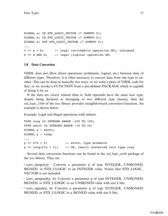
Example: Legal and illegal operations with std_logic_vector.
LIBRARY ieee;
USE ieee.std_logic_1164.all; -- no extra package required
...
SIGNAL a: IN STD_LOGIC_VECTOR (7 DOWNTO 0);
SIGNAL b: IN STD_LOGIC_VECTOR (7 DOWNTO 0);
SIGNAL x: OUT STD_LOGIC_VECTOR (7 DOWNTO 0);
...
v <= a + b; -- illegal (arithmetic operation not OK)
w <= a AND b; -- legal (logical operation OK)
Despite the constraint mentioned above, there is a simple way of allowing data of
type STD_LOGIC_VECTOR to participate directly in arithmetic operations. For
that, the ieee library provides two packages, std_logic_signed and std_logic_unsigned,
which allow operations with STD_LOGIC_VECTOR data to be performed as if the
data were of type SIGNED or UNSIGNED, respectively.
Example: Arithmetic operations with std_logic_vector.
LIBRARY ieee;
USE ieee.std_logic_1164.all;
USE ieee.std_logic_unsigned.all; -- extra package included
...
36 Chapter 3
TLFeBOOK
SIGNAL a: IN STD_LOGIC_VECTOR (7 DOWNTO 0);
SIGNAL b: IN STD_LOGIC_VECTOR (7 DOWNTO 0);
SIGNAL x: OUT STD_LOGIC_VECTOR (7 DOWNTO 0);
...
v <= a + b; -- legal (arithmetic operation OK), unsigned
w <= a AND b; -- legal (logical operation OK)
3.8 Data Conversion
VHDL does not allow direct operations (arithmetic, logical, etc.) between data of
di¤erent types. Therefore, it is often necessary to convert data from one type to an-
other. This can be done in basically two ways: or we write a piece of VHDL code for
that, or we invoke a FUNCTION from a pre-defined PACKAGE which is capable
of doing it for us.
If the data are closely related (that is, both operands have the same base type,
despite being declared as belonging to two di¤erent type classes), then the
std_logic_1164 of the ieee library provides straightforward conversion functions. An
example is shown below.
Example: Legal and illegal operations with subsets.
TYPE long IS INTEGER RANGE -100 TO 100;
TYPE short IS INTEGER RANGE -10 TO 10;
SIGNAL x : short;
SIGNAL y : long;
...
y <= 2*x + 5; -- error, type mismatch
y <= long(2*x + 5); -- OK, result converted into type long
Several data conversion functions can be found in the std_logic_arith package of
the ieee library. They are:
� conv_integer(p) : Converts a parameter p of type INTEGER, UNSIGNED,
SIGNED, or STD_ULOGIC to an INTEGER value. Notice that STD_LOGIC_
VECTOR is not included.
� conv_unsigned(p, b): Converts a parameter p of type INTEGER, UNSIGNED,
SIGNED, or STD_ULOGIC to an UNSIGNED value with size b bits.
� conv_signed(p, b): Converts a parameter p of type INTEGER, UNSIGNED,
SIGNED, or STD_ULOGIC to a SIGNED value with size b bits.
Data Types 37
TLFeBOOK
� conv_std_logic_vector(p, b): Converts a parameter p of type INTEGER, UN-
SIGNED, SIGNED, or STD_LOGIC to a STD_LOGIC_VECTOR value with size
b bits.
Example: Data conversion.
LIBRARY ieee;
USE ieee.std_logic_1164.all;
USE ieee.std_logic_arith.all;
...
SIGNAL a: IN UNSIGNED (7 DOWNTO 0);
SIGNAL b: IN UNSIGNED (7 DOWNTO 0);
SIGNAL y: OUT STD_LOGIC_VECTOR (7 DOWNTO 0);
...
y <= CONV_STD_LOGIC_VECTOR ((a+b), 8);
-- Legal operation: a+b is converted from UNSIGNED to an
-- 8-bit STD_LOGIC_VECTOR value, then assigned to y.
Another alternative was already mentioned in the previous section. It consists of
using the std_logic_signed or the std_logic_unsigned package from the ieee library.
Such packages allow operations with STD_LOGIC_VECTOR data to be performed
as if the data were of type SIGNED or UNSIGNED, respectively.
Besides the data conversion functions described above, several others are often
o¤ered by synthesis tool vendors.
3.9 Summary
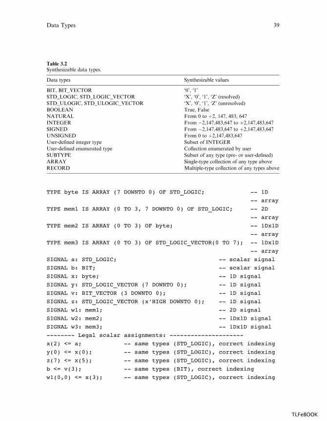
The fundamental synthesizable VHDL data types are summarized in table 3.2.
3.10 Additional Examples
We close this chapter with the presentation of additional examples illustrating the
specification and use of data types. The development of actual designs from scratch
will only be possible after we conclude laying out the basic foundations of VHDL
(chapters 1 to 4).
Example 3.1: Dealing with Data Types
The legal and illegal assignments presented next are based on the following type
definitions and signal declarations:
38 Chapter 3
TLFeBOOK
TYPE byte IS ARRAY (7 DOWNTO 0) OF STD_LOGIC; -- 1D
-- array
TYPE mem1 IS ARRAY (0 TO 3, 7 DOWNTO 0) OF STD_LOGIC; -- 2D
-- array
TYPE mem2 IS ARRAY (0 TO 3) OF byte; -- 1Dx1D
-- array
TYPE mem3 IS ARRAY (0 TO 3) OF STD_LOGIC_VECTOR(0 TO 7); -- 1Dx1D
-- array
SIGNAL a: STD_LOGIC; -- scalar signal
SIGNAL b: BIT; -- scalar signal
SIGNAL x: byte; -- 1D signal
SIGNAL y: STD_LOGIC_VECTOR (7 DOWNTO 0); -- 1D signal
SIGNAL v: BIT_VECTOR (3 DOWNTO 0); -- 1D signal
SIGNAL z: STD_LOGIC_VECTOR (x'HIGH DOWNTO 0); -- 1D signal
SIGNAL w1: mem1; -- 2D signal
SIGNAL w2: mem2; -- 1Dx1D signal
SIGNAL w3: mem3; -- 1Dx1D signal
-------- Legal scalar assignments: ---------------------
x(2) <= a; -- same types (STD_LOGIC), correct indexing
y(0) <= x(0); -- same types (STD_LOGIC), correct indexing
z(7) <= x(5); -- same types (STD_LOGIC), correct indexing
b <= v(3); -- same types (BIT), correct indexing
w1(0,0) <= x(3); -- same types (STD_LOGIC), correct indexing
Table 3.2Synthesizable data types.
Data types Synthesizable values
BIT, BIT_VECTOR ‘0’, ‘1’
STD_LOGIC, STD_LOGIC_VECTOR ‘X’, ‘0’, ‘1’, ‘Z’ (resolved)
STD_ULOGIC, STD_ULOGIC_VECTOR ‘X’, ‘0’, ‘1’, ‘Z’ (unresolved)
BOOLEAN True, False
NATURAL From 0 to þ2, 147, 483, 647
INTEGER From �2,147,483,647 to þ2,147,483,647
SIGNED From �2,147,483,647 to þ2,147,483,647
UNSIGNED From 0 to þ2,147,483,647
User-defined integer type Subset of INTEGER
User-defined enumerated type Collection enumerated by user
SUBTYPE Subset of any type (pre- or user-defined)
ARRAY Single-type collection of any type above
RECORD Multiple-type collection of any types above
Data Types 39
TLFeBOOK

w1(2,5) <= y(7); -- same types (STD_LOGIC), correct indexing
w2(0)(0) <= x(2); -- same types (STD_LOGIC), correct indexing
w2(2)(5) <= y(7); -- same types (STD_LOGIC), correct indexing
w1(2,5) <= w2(3)(7); -- same types (STD_LOGIC), correct indexing
------- Illegal scalar assignments: --------------------
b <= a; -- type mismatch (BIT x STD_LOGIC)
w1(0)(2) <= x(2); -- index of w1 must be 2D
w2(2,0) <= a; -- index of w2 must be 1Dx1D
------- Legal vector assignments: ----------------------
x <= "11111110";
y <= ('1','1','1','1','1','1','0','Z');
z <= "11111" & "000";
x <= (OTHERS => '1');
y <= (7 =>'0', 1 =>'0', OTHERS => '1');
z <= y;
y(2 DOWNTO 0) <= z(6 DOWNTO 4);
w2(0)(7 DOWNTO 0) <= "11110000";
w3(2) <= y;
z <= w3(1);
z(5 DOWNTO 0) <= w3(1)(2 TO 7);
w3(1) <= "00000000";
w3(1) <= (OTHERS => '0');
w2 <= ((OTHERS=>'0'),(OTHERS=>'0'),(OTHERS=>'0'),(OTHERS=>'0'));
w3 <= ("11111100", ('0','0','0','0','Z','Z','Z','Z',),
(OTHERS=>'0'), (OTHERS=>'0'));
w1 <= ((OTHERS=>'Z'), "11110000" ,"11110000", (OTHERS=>'0'));
------ Illegal array assignments: ----------------------
x <= y; -- type mismatch
y(5 TO 7) <= z(6 DOWNTO 0); -- wrong direction of y
w1 <= (OTHERS => '1'); -- w1 is a 2D array
w1(0, 7 DOWNTO 0) <="11111111"; -- w1 is a 2D array
w2 <= (OTHERS => 'Z'); -- w2 is a 1Dx1D array
w2(0, 7 DOWNTO 0) <= "11110000"; -- index should be 1Dx1D
-- Example of data type independent array initialization:
FOR i IN 0 TO 3 LOOP
FOR j IN 7 DOWNTO 0 LOOP
x(j) <= '0';
y(j) <= '0'
40 Chapter 3
TLFeBOOK

z(j) <= '0';
w1(i,j) <= '0';
w2(i)(j) <= '0';
w3(i)(j) <= '0';
END LOOP;
END LOOP;
---------------------------------------------------------
Example 3.2: Single Bit Versus Bit Vector
This example illustrates the di¤erence between a single bit assignment and a bit
vector assignment (that is, BIT versus BIT_VECTOR, STD_LOGIC versus STD_
LOGIC_VECTOR, or STD_ULOGIC versus STD_ULOGIC_VECTOR).
Two VHDL codes are presented below. Both perform the AND operation be-
tween the input signals and assign the result to the output signal. The only di¤erence
between them is the number of bits in the input and output ports (one bit in the first,
four bits in the second). The circuits inferred from these codes are shown in figure
3.2.
----------------------------
ENTITY and2 IS
PORT (a, b: IN BIT;
x: OUT BIT);
END and2;
-----------------------------------
ENTITY and2 IS
PORT (a, b: IN BIT_VECTOR (0 TO 3);
x: OUT BIT_VECTOR (0 TO 3));
END and2;
----------------------------
ARCHITECTURE and2 OF and2 IS
BEGIN
x <= a AND b;
END and2;
----------------------------
-----------------------------------
ARCHITECTURE and2 OF and2 IS
BEGIN
x <= a AND b;
END and2;
-----------------------------------
Example 3.3: Adder
Figure 3.3 shows the top-level diagram of a 4-bit adder. The circuit has two inputs
(a, b) and one output (sum). Two solutions are presented. In the first, all signals are
of type SIGNED, while in the second the output is of type INTEGER. Notice in
solution 2 that a conversion function was used in line 13, for the type of aþ b does
not match that of sum. Notice also the inclusion of the std_logic_arith package (line
4 of each solution), which specifies the SIGNED data type. Recall that a SIGNED
value is represented like a vector; that is, similar to STD_LOGIC_VECTOR, not
like an INTEGER.
Data Types 41
TLFeBOOK

1 ----- Solution 1: in/out=SIGNED ----------
2 LIBRARY ieee;
3 USE ieee.std_logic_1164.all;
4 USE ieee.std_logic_arith.all;
5 ------------------------------------------
6 ENTITY adder1 IS
7 PORT ( a, b : IN SIGNED (3 DOWNTO 0);
8 sum : OUT SIGNED (4 DOWNTO 0));
9 END adder1;
10 ------------------------------------------
11 ARCHITECTURE adder1 OF adder1 IS
12 BEGIN
13 sum <= a + b;
14 END adder1;
15 ------------------------------------------
a
bx
a(0)
b(0)x(0)
a(1)
b(1)x(1)
a(2)
b(2)x(2)
a(3)
b(3)x(3)
Figure 3.2Circuits inferred from the codes of example 3.2.
a (3:0)
b (3:0)sum (4:0)+
Figure 3.34-bit adder of example 3.3.
42 Chapter 3
TLFeBOOK
1 ------ Solution 2: out=INTEGER -----------
2 LIBRARY ieee;
3 USE ieee.std_logic_1164.all;
4 USE ieee.std_logic_arith.all;
5 ------------------------------------------
6 ENTITY adder2 IS
7 PORT ( a, b : IN SIGNED (3 DOWNTO 0);
8 sum : OUT INTEGER RANGE -16 TO 15);
9 END adder2;
10 ------------------------------------------
11 ARCHITECTURE adder2 OF adder2 IS
12 BEGIN
13 sum <= CONV_INTEGER(a + b);
14 END adder2;
15 ------------------------------------------
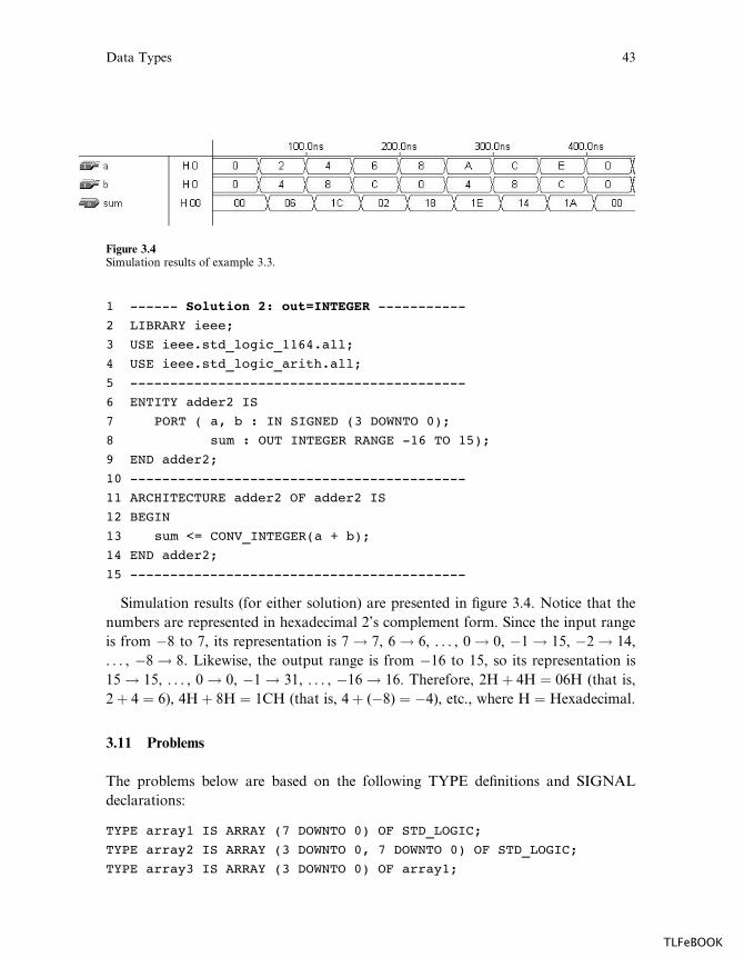
Simulation results (for either solution) are presented in figure 3.4. Notice that the
numbers are represented in hexadecimal 2’s complement form. Since the input range
is from �8 to 7, its representation is 7 ! 7, 6 ! 6, . . . , 0 ! 0, �1 ! 15, �2 ! 14,
. . . , �8 ! 8. Likewise, the output range is from �16 to 15, so its representation is
15 ! 15, . . . , 0 ! 0, �1 ! 31, . . . , �16 ! 16. Therefore, 2Hþ 4H ¼ 06H (that is,
2þ 4 ¼ 6), 4Hþ 8H ¼ 1CH (that is, 4þ (�8) ¼ �4), etc., where H ¼ Hexadecimal.
3.11 Problems
The problems below are based on the following TYPE definitions and SIGNAL
declarations:
TYPE array1 IS ARRAY (7 DOWNTO 0) OF STD_LOGIC;
TYPE array2 IS ARRAY (3 DOWNTO 0, 7 DOWNTO 0) OF STD_LOGIC;
TYPE array3 IS ARRAY (3 DOWNTO 0) OF array1;
Figure 3.4Simulation results of example 3.3.
Data Types 43
TLFeBOOK
SIGNAL a : BIT;
SIGNAL b : STD_LOGIC;:
SIGNAL x : array1;
SIGNAL y : array2;
SIGNAL w : array3;
SIGNAL z : STD_LOGIC_VECTOR (7 DOWNTO 0);
Problem 3.1
Determine the dimensionality (scalar, 1D, 2D, or 1Dx1D) of the signals given. Also,
write down a numeric example for each signal.
Problem 3.2
Determine which among the assignments in table P3.2 are legal and which are illegal.
Briefly justify your answers. Also, determine the dimensionality of each assignment
(on both sides).
Problem 3.3: Subtypes
Consider the pre-defined data types INTEGER and STD_LOGIC_VECTOR. Con-
sider also the user-defined types ARRAY1 and ARRAY2 specified above. For each,
write down a possible SUBTYPE.
Problem 3.4: ROM
Consider the implementation of a ROM (read-only memory). It can be done utiliz-
ing a 1Dx1D CONSTANT. Say that the ROM must be organized as a pile of eight
words of four bits each. Create an array called rom, then define a signal of type
rom capable of solving this problem. Choose the values to be stored in the ROM
and declare them along with your CONSTANT, that is, ‘‘CONSTANT my_rom:
rom :=(values);’’.
Problem 3.5: Simple Adder
Rewrite solution 1 of example 3.3, but this time with all input and output signals of
type STD_LOGIC_VECTOR. (Suggestion: review section 3.8).
44 Chapter 3
TLFeBOOK
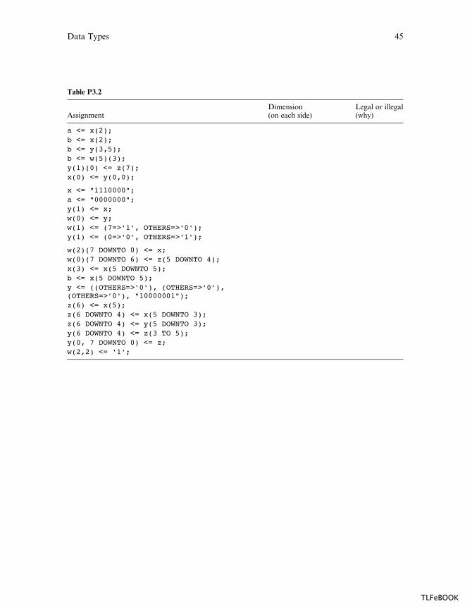
Table P3.2
AssignmentDimension(on each side)
Legal or illegal(why)
a <= x(2);b <= x(2);b <= y(3,5);b <= w(5)(3);y(1)(0) <= z(7);x(0) <= y(0,0);
x <= "1110000";a <= "0000000";y(1) <= x;w(0) <= y;w(1) <= (7=>'1', OTHERS=>'0');y(1) <= (0=>'0', OTHERS=>'1');
w(2)(7 DOWNTO 0) <= x;w(0)(7 DOWNTO 6) <= z(5 DOWNTO 4);x(3) <= x(5 DOWNTO 5);b <= x(5 DOWNTO 5);y <= ((OTHERS=>'0'), (OTHERS=>'0'),(OTHERS=>'0'), "10000001");z(6) <= x(5);z(6 DOWNTO 4) <= x(5 DOWNTO 3);z(6 DOWNTO 4) <= y(5 DOWNTO 3);y(6 DOWNTO 4) <= z(3 TO 5);y(0, 7 DOWNTO 0) <= z;w(2,2) <= '1';
Data Types 45
TLFeBOOK

TLFeBOOK
4 Operators and Attributes
The purpose of this chapter, along with the preceding chapters, is to lay the basic
foundations of VHDL, so in the next chapter we can start dealing with actual circuit
designs. It is indeed impossible—or little productive, at least—to write any code ef-
ficiently without undertaking first the sacrifice of understanding data types, operators,
and attributes well.
Operators and attributes constitute a relatively long list of general VHDL con-
structs, which are often examined only sparsely. We have collected them together in
a specific chapter in order to provide a complete and more consistent view.
At the end of the chapter, a few design examples will be presented. However, due
to the fact that this is still a ‘‘foundation’’ chapter, the examples are merely illustra-
tive, like those in the preceding chapters. As mentioned above, we will start dealing
with actual designs in chapter 5.
4.1 Operators
VHDL provides several kinds of pre-defined operators:
� Assignment operators
� Logical operators
� Arithmetic operators
� Relational operators
� Shift operators
� Concatenation operators
Each of these categories is described below.
Assignment Operators
Are used to assign values to signals, variables, and constants. They are:
<¼ Used to assign a value to a SIGNAL.
:¼ Used to assign a value to a VARIABLE, CONSTANT, or GENERIC. Used
also for establishing initial values.
¼> Used to assign values to individual vector elements or with OTHERS.
Example: Consider the following signal and variable declarations:
SIGNAL x : STD_LOGIC;
VARIABLE y : STD_LOGIC_VECTOR(3 DOWNTO 0); -- Leftmost bit is MSB
TLFeBOOK
SIGNAL w: STD_LOGIC_VECTOR(0 TO 7); -- Rightmost bit is
-- MSB
Then the following assignments are legal:
x <= '1'; -- '1' is assigned to SIGNAL x using "<="
y := "0000"; -- "0000" is assigned to VARIABLE y using ":="
w <= "10000000"; -- LSB is '1', the others are '0'
w <= (0 =>'1', OTHERS =>'0'); -- LSB is '1', the others are '0'
Logical Operators
Used to perform logical operations. The data must be of type BIT, STD_LOGIC,
or STD_ULOGIC (or, obviously, their respective extensions, BIT_VECTOR,
STD_LOGIC_VECTOR, or STD_ULOGIC_VECTOR). The logical operators are:
� NOT
� AND
� OR
� NAND
� NOR
� XOR
� XNOR
Notes: The NOT operator has precedence over the others. The XNOR operator was
introduced in VHDL93.
Examples:
y <= NOT a AND b; -- (a'.b)
y <= NOT (a AND b); -- (a.b)'
y <= a NAND b; -- (a.b)'
Arithmetic Operators
Used to perform arithmetic operations. The data can be of type INTEGER,
SIGNED, UNSIGNED, or REAL (recall that the last cannot be synthesized di-
rectly). Also, if the std_logic_signed or the std_logic_unsigned package of the ieee
library is used, then STD_LOGIC_VECTOR can also be employed directly in addi-
tion and subtraction operations (as seen in section 3.6).
48 Chapter 4
TLFeBOOK
þ Addition
� Subtraction
* Multiplication
/ Division
** Exponentiation
MOD Modulus
REM Remainder
ABS Absolute value
There are no synthesis restrictions regarding addition and subtraction, and the
same is generally true for multiplication. For division, only power of two dividers
(shift operation) are allowed. For exponentiation, only static values of base and ex-
ponent are accepted. Regarding the mod and rem operators, y mod x returns the re-
mainder of y/x with the signal of x, while y rem x returns the remainder of y/x with
the signal of y. Finally, abs returns the absolute value. With respect to the last three
operators (mod, rem, abs), there generally is little or no synthesis support.
Comparison Operators
Used for making comparisons. The data can be of any of the types listed above. The
relational (comparison) operators are:
¼ Equal to
=¼ Not equal to
< Less than
> Greater than
<¼ Less than or equal to
>¼ Greater than or equal to
Shift Operators
Used for shifting data. They were introduced in VHDL93. Their syntax is the fol-
lowing: 3left operand4 3shift operation4 3right operand4. The left operand must be
of type BIT_VECTOR, while the right operand must be an INTEGER (þ or � in
front of it is accepted). The shift operators are:
� sll Shift left logic – positions on the right are filled with ‘0’s
� srl Shift right logic – positions on the left are filled with ‘0’s
Operators and Attributes 49
TLFeBOOK

Data Attributes
The pre-defined, synthesizable data attributes are the following:
� d’LOW: Returns lower array index
� d’HIGH: Returns upper array index
� d’LEFT: Returns leftmost array index
� d’RIGHT: Returns rightmost array index
� d’LENGTH: Returns vector size
� d’RANGE: Returns vector range
� d’REVERSE_RANGE: Returns vector range in reverse order
Example: Consider the following signal:
SIGNAL d : STD_LOGIC_VECTOR (7 DOWNTO 0);
Then:
d'LOW=0, d'HIGH=7, d'LEFT=7, d'RIGHT=0, d'LENGTH=8,
d'RANGE=(7 downto 0), d'REVERSE_RANGE=(0 to 7).
Example: Consider the following signal:
SIGNAL x: STD_LOGIC_VECTOR (0 TO 7);
Then all four LOOP statements below are synthesizable and equivalent.
FOR i IN RANGE (0 TO 7) LOOP ...
FOR i IN x'RANGE LOOP ...
FOR i IN RANGE (x'LOW TO x'HIGH) LOOP ...
FOR i IN RANGE (0 TO x'LENGTH-1) LOOP ...
If the signal is of enumerated type, then:
� d’VAL(pos): Returns value in the position specified
� d’POS(value): Returns position of the value specified
� d’LEFTOF(value): Returns value in the position to the left of the value specified
� d’VAL(row, column): Returns value in the position specified; etc.
There is little or no synthesis support for enumerated data type attributes.
Operators and Attributes 51
TLFeBOOK
Signal Attributes
Let us consider a signal s. Then:
� s’EVENT: Returns true when an event occurs on s
� s’STABLE: Returns true if no event has occurred on s
� s’ACTIVE: Returns true if s ¼ ‘1’
� s’QUIET 3time4: Returns true if no event has occurred during the time specified
� s’LAST_EVENT: Returns the time elapsed since last event
� s’LAST_ACTIVE: Returns the time elapsed since last s ¼ ‘1’
� s’LAST_VALUE: Returns the value of s before the last event; etc.
Though most signal attributes are for simulation purposes only, the first two in the
list above are synthesizable, s’EVENT being the most often used of them all.
Example: All four assignments shown below are synthesizable and equivalent. They
return TRUE when an event (a change) occurs on clk, AND if such event is upward
(in other words, when a rising edge occurs on clk).
IF (clk'EVENT AND clk='1')... -- EVENT attribute used
-- with IF
IF (NOT clk'STABLE AND clk='1')... -- STABLE attribute used
-- with IF
WAIT UNTIL (clk'EVENT AND clk='1'); -- EVENT attribute used
-- with WAIT
IF RISING_EDGE(clk)... -- call to a function
4.3 User-Defined Attributes
We saw above attributes of the type HIGH, RANGE, EVENT, etc. Those are all
pre-defined in VHDL87. However, VHDL also allows the construction of user-
defined attributes.
To employ a user-defined attribute, it must be declared and specified. The syntax is
the following:
Attribute declaration:
ATTRIBUTE attribute_name: attribute_type;
52 Chapter 4
TLFeBOOK
Attribute specification:
ATTRIBUTE attribute_name OF target_name: class IS value;
where:
attribute_type: any data type (BIT, INTEGER, STD_LOGIC_VECTOR, etc.)
class: TYPE, SIGNAL, FUNCTION, etc.
value: ‘0’, 27, ‘‘00 11 10 01’’, etc.
Example:
ATTRIBUTE number_of_inputs: INTEGER; -- declaration
ATTRIBUTE number_of_inputs OF nand3: SIGNAL IS 3; -- specification
...
inputs <= nand3'number_of_pins; -- attribute call, returns 3
Example: Enumerated encoding.
A popular user-defined attribute, which is provided by synthesis tool vendors, is the
enum_encoding attribute. By default, enumerated data types are encoded sequen-
tially. Thus, if we consider the enumerated data type color shown below:
TYPE color IS (red, green, blue, white);
its states will be encoded as red ¼ ‘‘00’’, green ¼ ‘‘01’’, blue ¼ ‘‘10’’, and white ¼‘‘11’’. Enum_encoding allows the default encoding (sequential) to be changed. Thus
the following encoding scheme could be employed, for example:
ATTRIBUTE enum_encoding OF color: TYPE IS "11 00 10 01";
A user-defined attribute can be declared anywhere, except in a PACKAGE
BODY. When not recognized by the synthesis tool, it is simply ignored, or a warning
is issued.
4.4 Operator Overloading
We have just seen that attributes can be user-defined. The same is true for operators.
As an example, let us consider the pre-defined arithmetic operators seen in section
4.1 (þ, �, *, /, etc.). They specify arithmetic operations between data of certain types
Operators and Attributes 53
TLFeBOOK
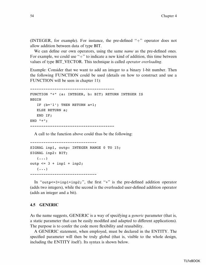
(INTEGER, for example). For instance, the pre-defined ‘‘þ’’ operator does not
allow addition between data of type BIT.
We can define our own operators, using the same name as the pre-defined ones.
For example, we could use ‘‘þ’’ to indicate a new kind of addition, this time between
values of type BIT_VECTOR. This technique is called operator overloading.
Example: Consider that we want to add an integer to a binary 1-bit number. Then
the following FUNCTION could be used (details on how to construct and use a
FUNCTION will be seen in chapter 11):
--------------------------------------
FUNCTION "+" (a: INTEGER, b: BIT) RETURN INTEGER IS
BEGIN
IF (b='1') THEN RETURN a+1;
ELSE RETURN a;
END IF;
END "+";
--------------------------------------
A call to the function above could thus be the following:
------------------------------
SIGNAL inp1, outp: INTEGER RANGE 0 TO 15;
SIGNAL inp2: BIT;
(...)
outp <= 3 + inp1 + inp2;
(...)
------------------------------
In ‘‘outp<=3+inp1+inp2;’’, the first ‘‘+’’ is the pre-defined addition operator
(adds two integers), while the second is the overloaded user-defined addition operator
(adds an integer and a bit).
4.5 GENERIC
As the name suggests, GENERIC is a way of specifying a generic parameter (that is,
a static parameter that can be easily modified and adapted to di¤erent applications).
The purpose is to confer the code more flexibility and reusability.
A GENERIC statement, when employed, must be declared in the ENTITY. The
specified parameter will then be truly global (that is, visible to the whole design,
including the ENTITY itself ). Its syntax is shown below.
54 Chapter 4
TLFeBOOK

GENERIC (parameter_name : parameter_type := parameter_value);
Example: The GENERIC statement below specifies a parameter called n, of type
INTEGER, whose default value is 8. Therefore, whenever n is found in the ENTITY
itself or in the ARCHITECTURE (one or more) that follows, its value will be
assumed to be 8.
ENTITY my_entity IS
GENERIC (n : INTEGER := 8);
PORT (...);
END my_entity;
ARCHITECTURE my_architecture OF my_entity IS
...
END my_architecture:
More than one GENERIC parameter can be specified in an ENTITY. For
example:
GENERIC (n: INTEGER := 8; vector: BIT_VECTOR := "00001111");
Complete design examples, further illustrating the use of GENERIC and other
attributes and operators, are presented below.
4.6 Examples
We show now a few complete design examples, with the purpose of further illus-
trating the use of operators, attributes and GENERIC. Recall, however, that so
far we have just worked on establishing the basic foundations of VHDL, with
the formal discussion on coding techniques starting only in the next chapter (chap-
ter 5). Therefore, a first-time VHDL student should not feel discouraged if the
constructs in the examples look still unfamiliar. Instead, you may have a look at
the examples now, and then, after studying chapters 5 to 7, return and reexamine
them.
Example 4.1: Generic Decoder
Figure 4.1 shows the top-level diagram of a generic m-by-n decoder. The circuit has
two inputs, sel (m bits) and ena (single bit), and one output, x (n bits). We assume
that n is a power of two, so m ¼ log2n. If ena ¼ ‘0’, then all bits of x should be high;
Operators and Attributes 55
TLFeBOOK
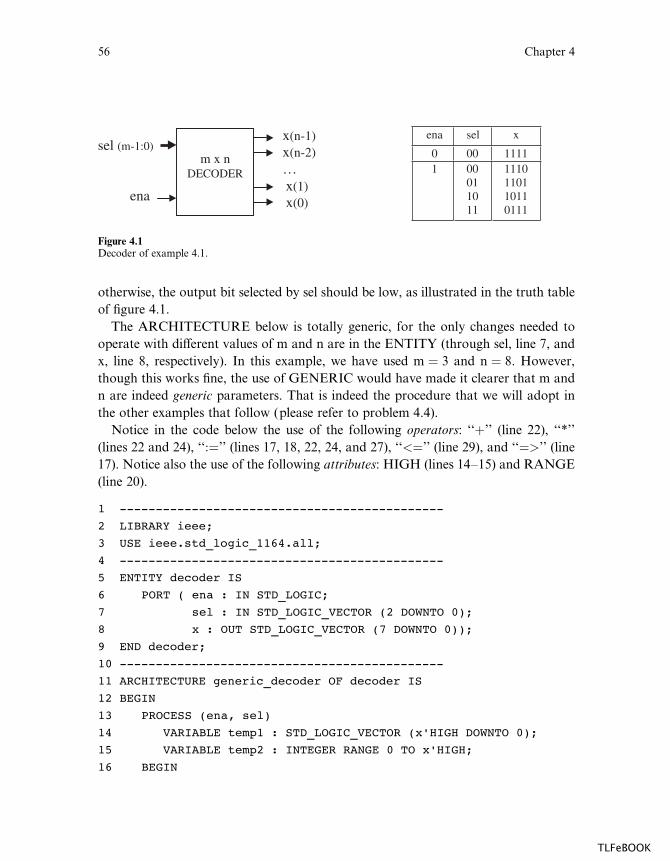
otherwise, the output bit selected by sel should be low, as illustrated in the truth table
of figure 4.1.
The ARCHITECTURE below is totally generic, for the only changes needed to
operate with di¤erent values of m and n are in the ENTITY (through sel, line 7, and
x, line 8, respectively). In this example, we have used m ¼ 3 and n ¼ 8. However,
though this works fine, the use of GENERIC would have made it clearer that m and
n are indeed generic parameters. That is indeed the procedure that we will adopt in
the other examples that follow (please refer to problem 4.4).
Notice in the code below the use of the following operators: ‘‘þ’’ (line 22), ‘‘*’’
(lines 22 and 24), ‘‘:¼’’ (lines 17, 18, 22, 24, and 27), ‘‘<¼’’ (line 29), and ‘‘¼>’’ (line
17). Notice also the use of the following attributes: HIGH (lines 14–15) and RANGE
(line 20).
1 ---------------------------------------------
2 LIBRARY ieee;
3 USE ieee.std_logic_1164.all;
4 ---------------------------------------------
5 ENTITY decoder IS
6 PORT ( ena : IN STD_LOGIC;
7 sel : IN STD_LOGIC_VECTOR (2 DOWNTO 0);
8 x : OUT STD_LOGIC_VECTOR (7 DOWNTO 0));
9 END decoder;
10 ---------------------------------------------
11 ARCHITECTURE generic_decoder OF decoder IS
12 BEGIN
13 PROCESS (ena, sel)
14 VARIABLE temp1 : STD_LOGIC_VECTOR (x'HIGH DOWNTO 0);
15 VARIABLE temp2 : INTEGER RANGE 0 TO x'HIGH;
16 BEGIN
ena sel x
11110 00001011011
1110110110110111
sel (m-1:0)
ena
x(n-1)x(n-2)…x(1)x(0)
m x n DECODER
Figure 4.1Decoder of example 4.1.
56 Chapter 4
TLFeBOOK
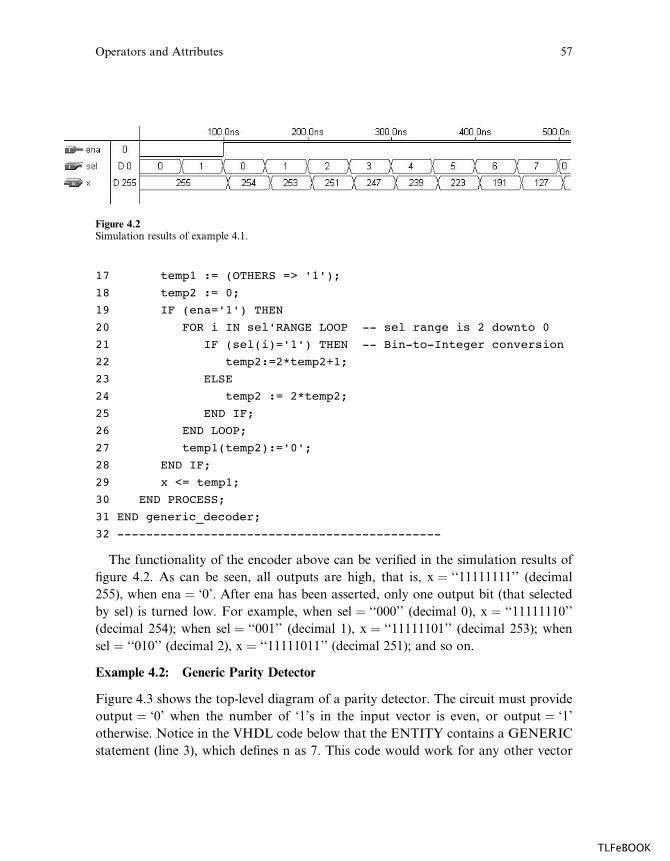
17 temp1 := (OTHERS => '1');
18 temp2 := 0;
19 IF (ena='1') THEN
20 FOR i IN sel'RANGE LOOP -- sel range is 2 downto 0
21 IF (sel(i)='1') THEN -- Bin-to-Integer conversion
22 temp2:=2*temp2+1;
23 ELSE
24 temp2 := 2*temp2;
25 END IF;
26 END LOOP;
27 temp1(temp2):='0';
28 END IF;
29 x <= temp1;
30 END PROCESS;
31 END generic_decoder;
32 ---------------------------------------------
The functionality of the encoder above can be verified in the simulation results of
figure 4.2. As can be seen, all outputs are high, that is, x ¼ ‘‘11111111’’ (decimal
255), when ena ¼ ‘0’. After ena has been asserted, only one output bit (that selected
by sel) is turned low. For example, when sel ¼ ‘‘000’’ (decimal 0), x ¼ ‘‘11111110’’
(decimal 254); when sel ¼ ‘‘001’’ (decimal 1), x ¼ ‘‘11111101’’ (decimal 253); when
sel ¼ ‘‘010’’ (decimal 2), x ¼ ‘‘11111011’’ (decimal 251); and so on.
Example 4.2: Generic Parity Detector
Figure 4.3 shows the top-level diagram of a parity detector. The circuit must provide
output ¼ ‘0’ when the number of ‘1’s in the input vector is even, or output ¼ ‘1’
otherwise. Notice in the VHDL code below that the ENTITY contains a GENERIC
statement (line 3), which defines n as 7. This code would work for any other vector
Figure 4.2Simulation results of example 4.1.
Operators and Attributes 57
TLFeBOOK
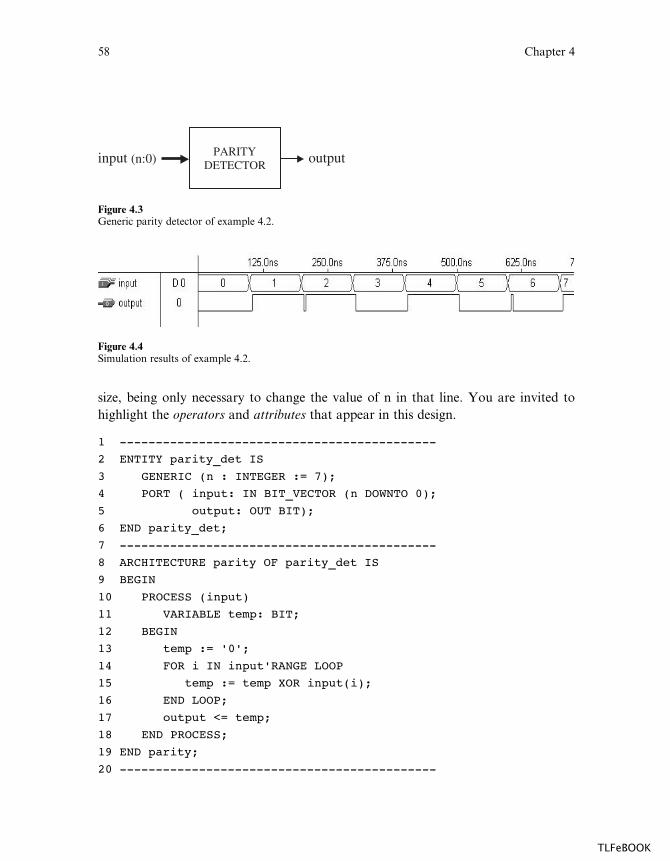
size, being only necessary to change the value of n in that line. You are invited to
highlight the operators and attributes that appear in this design.
1 --------------------------------------------
2 ENTITY parity_det IS
3 GENERIC (n : INTEGER := 7);
4 PORT ( input: IN BIT_VECTOR (n DOWNTO 0);
5 output: OUT BIT);
6 END parity_det;
7 --------------------------------------------
8 ARCHITECTURE parity OF parity_det IS
9 BEGIN
10 PROCESS (input)
11 VARIABLE temp: BIT;
12 BEGIN
13 temp := '0';
14 FOR i IN input'RANGE LOOP
15 temp := temp XOR input(i);
16 END LOOP;
17 output <= temp;
18 END PROCESS;
19 END parity;
20 --------------------------------------------
input (n:0) outputPARITYDETECTOR
Figure 4.3Generic parity detector of example 4.2.
Figure 4.4Simulation results of example 4.2.
58 Chapter 4
TLFeBOOK
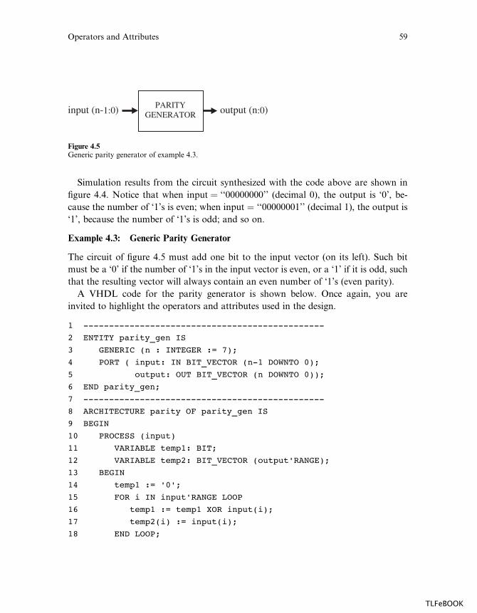
Simulation results from the circuit synthesized with the code above are shown in
figure 4.4. Notice that when input ¼ ‘‘00000000’’ (decimal 0), the output is ‘0’, be-
cause the number of ‘1’s is even; when input ¼ ‘‘00000001’’ (decimal 1), the output is
‘1’, because the number of ‘1’s is odd; and so on.
Example 4.3: Generic Parity Generator
The circuit of figure 4.5 must add one bit to the input vector (on its left). Such bit
must be a ‘0’ if the number of ‘1’s in the input vector is even, or a ‘1’ if it is odd, such
that the resulting vector will always contain an even number of ‘1’s (even parity).
A VHDL code for the parity generator is shown below. Once again, you are
invited to highlight the operators and attributes used in the design.
1 -----------------------------------------------
2 ENTITY parity_gen IS
3 GENERIC (n : INTEGER := 7);
4 PORT ( input: IN BIT_VECTOR (n-1 DOWNTO 0);
5 output: OUT BIT_VECTOR (n DOWNTO 0));
6 END parity_gen;
7 -----------------------------------------------
8 ARCHITECTURE parity OF parity_gen IS
9 BEGIN
10 PROCESS (input)
11 VARIABLE temp1: BIT;
12 VARIABLE temp2: BIT_VECTOR (output'RANGE);
13 BEGIN
14 temp1 := '0';
15 FOR i IN input'RANGE LOOP
16 temp1 := temp1 XOR input(i);
17 temp2(i) := input(i);
18 END LOOP;
input (n-1:0) PARITYGENERATOR output (n:0)
Figure 4.5Generic parity generator of example 4.3.
Operators and Attributes 59
TLFeBOOK
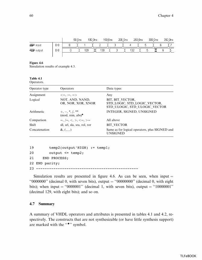
19 temp2(output'HIGH) := temp1;
20 output <= temp2;
21 END PROCESS;
22 END parity;
23 -----------------------------------------------
Simulation results are presented in figure 4.6. As can be seen, when input ¼‘‘0000000’’ (decimal 0, with seven bits), output ¼ ‘‘00000000’’ (decimal 0, with eight
bits); when input ¼ ‘‘0000001’’ (decimal 1, with seven bits), output ¼ ‘‘10000001’’
(decimal 129, with eight bits); and so on.
4.7 Summary
A summary of VHDL operators and attributes is presented in tables 4.1 and 4.2, re-
spectively. The constructs that are not synthesizable (or have little synthesis support)
are marked with the ‘‘) ’’ symbol.
Figure 4.6Simulation results of example 4.3.
Table 4.1Operators.
Operator type Operators Data types
Assignment <¼, :¼, ¼> Any
Logical NOT, AND, NAND,OR, NOR, XOR, XNOR
BIT, BIT_VECTOR,STD_LOGIC, STD_LOGIC_VECTOR,STD_ULOGIC, STD_ULOGIC_VECTOR
Arithmetic þ, �, *, /, **(mod, rem, abs))
INTEGER, SIGNED, UNSIGNED
Comparison ¼, =¼, <, >, <¼, >¼ All above
Shift sll, srl, sla, sra, rol, ror BIT_VECTOR
Concatenation &, ( , , , ) Same as for logical operators, plus SIGNED andUNSIGNED
60 Chapter 4
TLFeBOOK
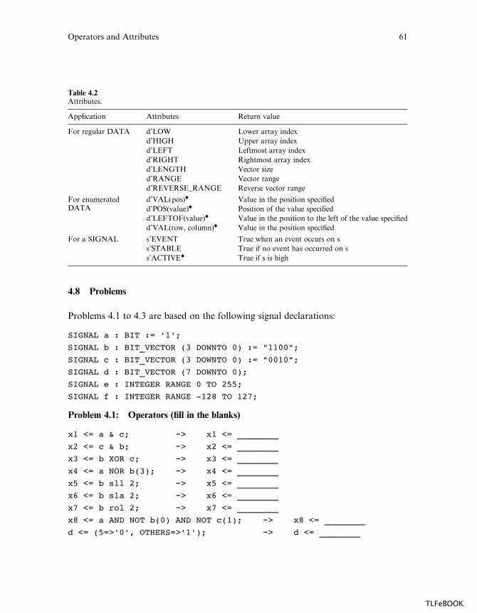
4.8 Problems
Problems 4.1 to 4.3 are based on the following signal declarations:
SIGNAL a : BIT := '1';
SIGNAL b : BIT_VECTOR (3 DOWNTO 0) := "1100";
SIGNAL c : BIT_VECTOR (3 DOWNTO 0) := "0010";
SIGNAL d : BIT_VECTOR (7 DOWNTO 0);
SIGNAL e : INTEGER RANGE 0 TO 255;
SIGNAL f : INTEGER RANGE -128 TO 127;
Problem 4.1: Operators (fill in the blanks)
x1 <= a & c; -> x1 <= ________
x2 <= c & b; -> x2 <= ________
x3 <= b XOR c; -> x3 <= ________
x4 <= a NOR b(3); -> x4 <= ________
x5 <= b sll 2; -> x5 <= ________
x6 <= b sla 2; -> x6 <= ________
x7 <= b rol 2; -> x7 <= ________
x8 <= a AND NOT b(0) AND NOT c(1); -> x8 <= ________
d <= (5=>'0', OTHERS=>'1'); -> d <= ________
Table 4.2Attributes.
Application Attributes Return value
For regular DATA d’LOW Lower array index
d’HIGH Upper array index
d’LEFT Leftmost array index
d’RIGHT Rightmost array index
d’LENGTH Vector size
d’RANGE Vector range
d’REVERSE_RANGE Reverse vector range
d’VAL(pos)) Value in the position specifiedFor enumeratedDATA d’POS(value)) Position of the value specified
d’LEFTOF(value)) Value in the position to the left of the value specified
d’VAL(row, column)) Value in the position specified
For a SIGNAL s’EVENT True when an event occurs on s
s’STABLE True if no event has occurred on s
s’ACTIVE) True if s is high
Operators and Attributes 61
TLFeBOOK
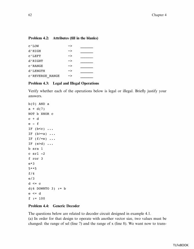
Problem 4.2: Attributes (fill in the blanks)
c'LOW -> ______
d'HIGH -> ______
c'LEFT -> ______
d'RIGHT -> ______
c'RANGE -> ______
d'LENGTH -> ______
c'REVERSE_RANGE -> ______
Problem 4.3: Legal and Illegal Operations
Verify whether each of the operations below is legal or illegal. Briefly justify your
answers.
b(0) AND a
a + d(7)
NOT b XNOR c
c + d
e - f
IF (b<c) ...
IF (b>=a) ...
IF (f/=e) ...
IF (e>d) ...
b sra 1
c srl -2
f ror 3
e*3
5**5
f/4
e/3
d <= c
d(6 DOWNTO 3) := b
e <= d
f := 100
Problem 4.4: Generic Decoder
The questions below are related to decoder circuit designed in example 4.1.
(a) In order for that design to operate with another vector size, two values must be
changed: the range of sel (line 7) and the range of x (line 8). We want now to trans-
62 Chapter 4
TLFeBOOK
form that design in a truly generic one. In order to do so, introduce a GENERIC
statement in the ENTITY, specifying the number of bits of sel (say, n ¼ 3), then re-
place the upper range limits of sel and x by an attribute which is a function of n.
Synthesize and simulate your circuit in order to verify its functionality.
(b) In example 4.1, a binary-to-integer conversion was implemented (lines 20–26).
This conversion could be avoided if sel had been declared as an INTEGER. Modify
the code, declaring sel as an INTEGER. The code should remain truly generic, so
the range of sel must be specified in terms of n. Synthesize and simulate your new
code.
Problem 4.5
List all operators, attributes and generics employed in examples 4.2 and 4.3.
Operators and Attributes 63
TLFeBOOK

TLFeBOOK

5 Concurrent Code
Having finished laying out the basic foundations of VHDL (chapters 1 to 4), we can
now concentrate on the design (code) itself.
VHDL code can be concurrent (parallel) or sequential. The former will be studied
in this chapter, while the latter will be seen in chapter 6. This division is very impor-
tant, for it allows a better understanding of which statements are intended for each
kind of code, as well as the consequences of using one or the other.
The concurrent statements in VHDL are WHEN and GENERATE. Besides them,
assignments using only operators (AND, NOT, þ, *, sll, etc.) can also be used to
construct concurrent code. Finally, a special kind of assignment, called BLOCK, can
also be employed in this kind of code.
5.1 Concurrent versus Sequential
We start this chapter by reviewing the fundamental di¤erences between combinational
logic and sequential logic, and by contrasting them with the di¤erences between con-
current code and sequential code.
Combinational versus Sequential Logic
By definition, combinational logic is that in which the output of the circuit depends
solely on the current inputs (figure 5.1(a)). It is then clear that, in principle, the system
requires no memory and can be implemented using conventional logic gates.
In contrast, sequential logic is defined as that in which the output does depend on
previous inputs (figure 5.1(b)). Therefore, storage elements are required, which are
connected to the combinational logic block through a feedback loop, such that now
the stored states (created by previous inputs) will also a¤ect the output of the circuit.
A common mistake is to think that any circuit that possesses storage elements
(flip-flops) is sequential. A RAM (Random Access Memory) is an example. A RAM
can be modeled as in figure 5.2. Notice that the storage elements appear in a forward
path rather than in a feedback loop. The memory-read operation depends only on
the address vector presently applied to the RAM input, with the retrieved value
having nothing to do with previous memory accesses.
Concurrent versus Sequential Code
VHDL code is inherently concurrent (parallel). Only statements placed inside a
PROCESS, FUNCTION, or PROCEDURE are sequential. Still, though within
these blocks the execution is sequential, the block, as a whole, is concurrent with any
other (external) statements. Concurrent code is also called dataflow code.
TLFeBOOK
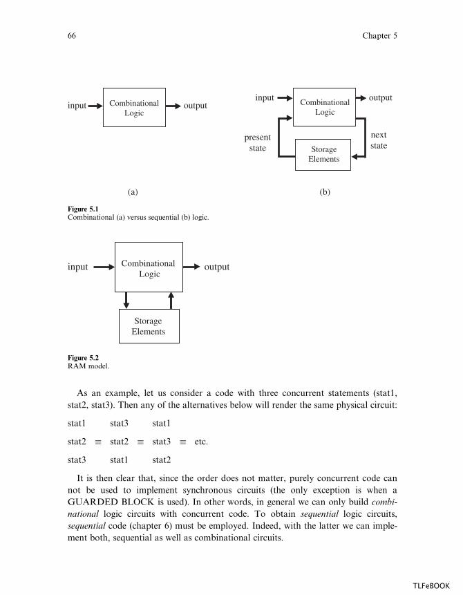
As an example, let us consider a code with three concurrent statements (stat1,
stat2, stat3). Then any of the alternatives below will render the same physical circuit:
stat1 stat3 stat1
stat2 C stat2 C stat3 C etc.
stat3 stat1 stat2
It is then clear that, since the order does not matter, purely concurrent code can
not be used to implement synchronous circuits (the only exception is when a
GUARDED BLOCK is used). In other words, in general we can only build combi-
national logic circuits with concurrent code. To obtain sequential logic circuits,
sequential code (chapter 6) must be employed. Indeed, with the latter we can imple-
ment both, sequential as well as combinational circuits.
(a) (b)
input outputCombinationalLogic
input
presentstate Storage
Elements
outputCombinationalLogic
nextstate
Figure 5.1Combinational (a) versus sequential (b) logic.
input
StorageElements
outputCombinationalLogic
Figure 5.2RAM model.
66 Chapter 5
TLFeBOOK
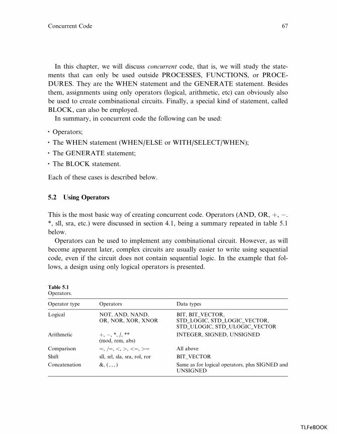
In this chapter, we will discuss concurrent code, that is, we will study the state-
ments that can only be used outside PROCESSES, FUNCTIONS, or PROCE-
DURES. They are the WHEN statement and the GENERATE statement. Besides
them, assignments using only operators (logical, arithmetic, etc) can obviously also
be used to create combinational circuits. Finally, a special kind of statement, called
BLOCK, can also be employed.
In summary, in concurrent code the following can be used:
� Operators;
� The WHEN statement (WHEN/ELSE or WITH/SELECT/WHEN);
� The GENERATE statement;
� The BLOCK statement.
Each of these cases is described below.
5.2 Using Operators
This is the most basic way of creating concurrent code. Operators (AND, OR, þ, �.
*, sll, sra, etc.) were discussed in section 4.1, being a summary repeated in table 5.1
below.
Operators can be used to implement any combinational circuit. However, as will
become apparent later, complex circuits are usually easier to write using sequential
code, even if the circuit does not contain sequential logic. In the example that fol-
lows, a design using only logical operators is presented.
Table 5.1Operators.
Operator type Operators Data types
Logical NOT, AND, NAND,OR, NOR, XOR, XNOR
BIT, BIT_VECTOR,STD_LOGIC, STD_LOGIC_VECTOR,STD_ULOGIC, STD_ULOGIC_VECTOR
Arithmetic þ, �, *, /, **(mod, rem, abs)
INTEGER, SIGNED, UNSIGNED
Comparison ¼, =¼, <, >, <¼, >¼ All above
Shift sll, srl, sla, sra, rol, ror BIT_VECTOR
Concatenation &, ( , , , ) Same as for logical operators, plus SIGNED andUNSIGNED
Concurrent Code 67
TLFeBOOK
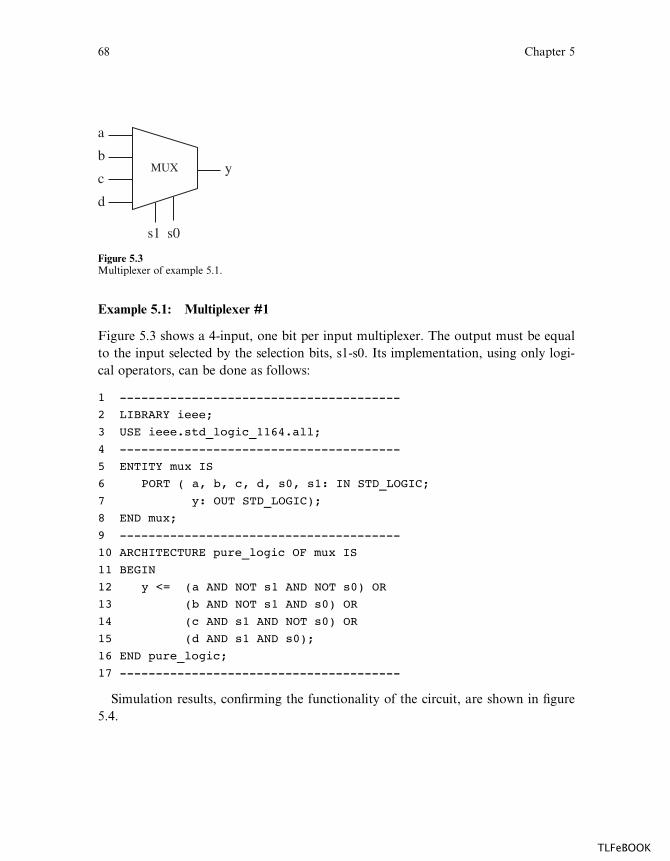
Example 5.1: Multiplexer #1
Figure 5.3 shows a 4-input, one bit per input multiplexer. The output must be equal
to the input selected by the selection bits, s1-s0. Its implementation, using only logi-
cal operators, can be done as follows:
1 ---------------------------------------
2 LIBRARY ieee;
3 USE ieee.std_logic_1164.all;
4 ---------------------------------------
5 ENTITY mux IS
6 PORT ( a, b, c, d, s0, s1: IN STD_LOGIC;
7 y: OUT STD_LOGIC);
8 END mux;
9 ---------------------------------------
10 ARCHITECTURE pure_logic OF mux IS
11 BEGIN
12 y <= (a AND NOT s1 AND NOT s0) OR
13 (b AND NOT s1 AND s0) OR
14 (c AND s1 AND NOT s0) OR
15 (d AND s1 AND s0);
16 END pure_logic;
17 ---------------------------------------
Simulation results, confirming the functionality of the circuit, are shown in figure
5.4.
s1 s0
a
b
c
d
yMUX
Figure 5.3Multiplexer of example 5.1.
68 Chapter 5
TLFeBOOK
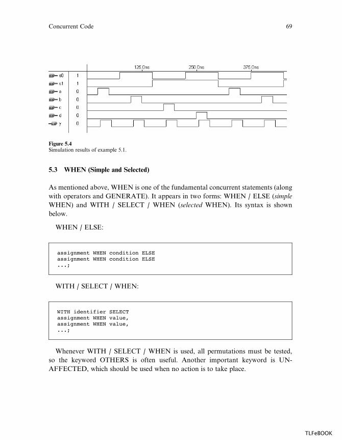
5.3 WHEN (Simple and Selected)
As mentioned above, WHEN is one of the fundamental concurrent statements (along
with operators and GENERATE). It appears in two forms: WHEN / ELSE (simple
WHEN) and WITH / SELECT / WHEN (selected WHEN). Its syntax is shown
below.
WHEN / ELSE:
assignment WHEN condition ELSEassignment WHEN condition ELSE...;
WITH / SELECT / WHEN:
WITH identifier SELECTassignment WHEN value,assignment WHEN value,...;
Whenever WITH / SELECT / WHEN is used, all permutations must be tested,
so the keyword OTHERS is often useful. Another important keyword is UN-
AFFECTED, which should be used when no action is to take place.
Figure 5.4Simulation results of example 5.1.
Concurrent Code 69
TLFeBOOK

Example:
------ With WHEN/ELSE -------------------------
outp <= "000" WHEN (inp='0' OR reset='1') ELSE
"001" WHEN ctl='1' ELSE
"010";
---- With WITH/SELECT/WHEN --------------------
WITH control SELECT
output <= "000" WHEN reset,
"111" WHEN set,
UNAFFECTED WHEN OTHERS;
-----------------------------------------------
Another important aspect related to the WHEN statement is that the ‘‘WHEN
value’’ shown in the syntax above can indeed take up three forms:
WHEN value -- single value
WHEN value1 to value2 -- range, for enumerated data types
-- only
WHEN value1 | value2 |... -- value1 or value2 or ...
Example 5.2: Multiplexer #2
This example shows the implementation of the same multiplexer of example 5.1, but
with a slightly di¤erent representation for the sel input (figure 5.5). However, in it
WHEN was employed instead of logical operators. Two solutions are presented: one
using WHEN/ELSE (simple WHEN) and the other with WITH/SELECT/WHEN
(selected WHEN). The experimental results are obviously similar to those obtained
in example 5.1.
sel (1:0)
a
b
c
d
yMUX
Figure 5.5Multiplexer of example 5.2.
70 Chapter 5
TLFeBOOK

1 ------- Solution 1: with WHEN/ELSE --------
2 LIBRARY ieee;
3 USE ieee.std_logic_1164.all;
4 -------------------------------------------
5 ENTITY mux IS
6 PORT ( a, b, c, d: IN STD_LOGIC;
7 sel: IN STD_LOGIC_VECTOR (1 DOWNTO 0);
8 y: OUT STD_LOGIC);
9 END mux;
10 -------------------------------------------
11 ARCHITECTURE mux1 OF mux IS
12 BEGIN
13 y <= a WHEN sel="00" ELSE
14 b WHEN sel="01" ELSE
15 c WHEN sel="10" ELSE
16 d;
17 END mux1;
18 -------------------------------------------
1 --- Solution 2: with WITH/SELECT/WHEN -----
2 LIBRARY ieee;
3 USE ieee.std_logic_1164.all;
4 -------------------------------------------
5 ENTITY mux IS
6 PORT ( a, b, c, d: IN STD_LOGIC;
7 sel: IN STD_LOGIC_VECTOR (1 DOWNTO 0);
8 y: OUT STD_LOGIC);
9 END mux;
10 -------------------------------------------
11 ARCHITECTURE mux2 OF mux IS
12 BEGIN
13 WITH sel SELECT
14 y <= a WHEN "00", -- notice "," instead of ";"
15 b WHEN "01",
16 c WHEN "10",
17 d WHEN OTHERS; -- cannot be "d WHEN "11" "
18 END mux2;
19 --------------------------------------------
Concurrent Code 71
TLFeBOOK
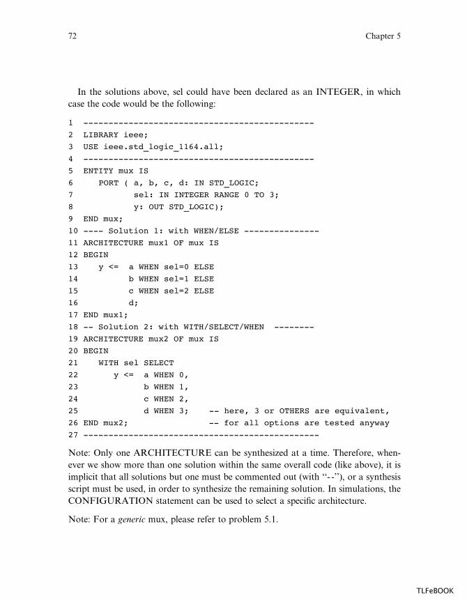
In the solutions above, sel could have been declared as an INTEGER, in which
case the code would be the following:
1 ----------------------------------------------
2 LIBRARY ieee;
3 USE ieee.std_logic_1164.all;
4 ----------------------------------------------
5 ENTITY mux IS
6 PORT ( a, b, c, d: IN STD_LOGIC;
7 sel: IN INTEGER RANGE 0 TO 3;
8 y: OUT STD_LOGIC);
9 END mux;
10 ---- Solution 1: with WHEN/ELSE ---------------
11 ARCHITECTURE mux1 OF mux IS
12 BEGIN
13 y <= a WHEN sel=0 ELSE
14 b WHEN sel=1 ELSE
15 c WHEN sel=2 ELSE
16 d;
17 END mux1;
18 -- Solution 2: with WITH/SELECT/WHEN --------
19 ARCHITECTURE mux2 OF mux IS
20 BEGIN
21 WITH sel SELECT
22 y <= a WHEN 0,
23 b WHEN 1,
24 c WHEN 2,
25 d WHEN 3; -- here, 3 or OTHERS are equivalent,
26 END mux2; -- for all options are tested anyway
27 -----------------------------------------------
Note: Only one ARCHITECTURE can be synthesized at a time. Therefore, when-
ever we show more than one solution within the same overall code (like above), it is
implicit that all solutions but one must be commented out (with ‘‘- -’’), or a synthesis
script must be used, in order to synthesize the remaining solution. In simulations, the
CONFIGURATION statement can be used to select a specific architecture.
Note: For a generic mux, please refer to problem 5.1.
72 Chapter 5
TLFeBOOK
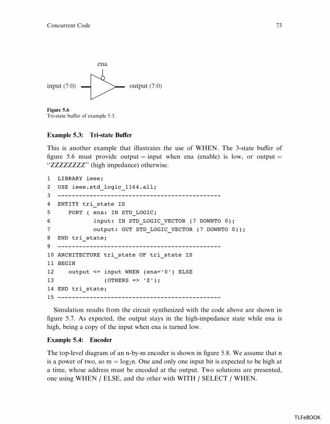
Example 5.3: Tri-state Bu¤er
This is another example that illustrates the use of WHEN. The 3-state bu¤er of
figure 5.6 must provide output ¼ input when ena (enable) is low, or output ¼‘‘ZZZZZZZZ’’ (high impedance) otherwise.
1 LIBRARY ieee;
2 USE ieee.std_logic_1164.all;
3 ----------------------------------------------
4 ENTITY tri_state IS
5 PORT ( ena: IN STD_LOGIC;
6 input: IN STD_LOGIC_VECTOR (7 DOWNTO 0);
7 output: OUT STD_LOGIC_VECTOR (7 DOWNTO 0));
8 END tri_state;
9 ----------------------------------------------
10 ARCHITECTURE tri_state OF tri_state IS
11 BEGIN
12 output <= input WHEN (ena='0') ELSE
13 (OTHERS => 'Z');
14 END tri_state;
15 ----------------------------------------------
Simulation results from the circuit synthesized with the code above are shown in
figure 5.7. As expected, the output stays in the high-impedance state while ena is
high, being a copy of the input when ena is turned low.
Example 5.4: Encoder
The top-level diagram of an n-by-m encoder is shown in figure 5.8. We assume that n
is a power of two, so m ¼ log2n. One and only one input bit is expected to be high at
a time, whose address must be encoded at the output. Two solutions are presented,
one using WHEN / ELSE, and the other with WITH / SELECT / WHEN.
input (7:0) output (7:0)
ena
Figure 5.6Tri-state bu¤er of example 5.3.
Concurrent Code 73
TLFeBOOK
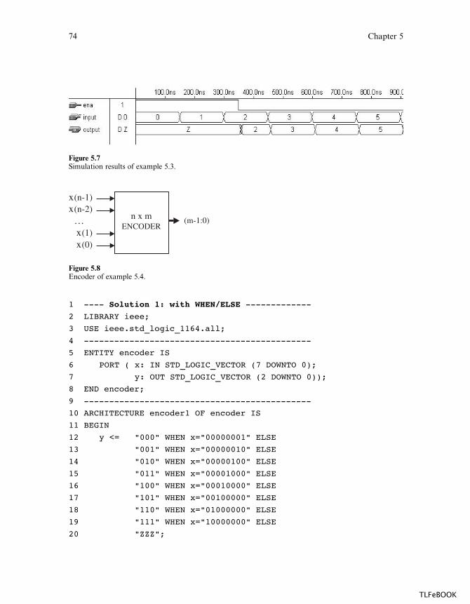
1 ---- Solution 1: with WHEN/ELSE -------------
2 LIBRARY ieee;
3 USE ieee.std_logic_1164.all;
4 ---------------------------------------------
5 ENTITY encoder IS
6 PORT ( x: IN STD_LOGIC_VECTOR (7 DOWNTO 0);
7 y: OUT STD_LOGIC_VECTOR (2 DOWNTO 0));
8 END encoder;
9 ---------------------------------------------
10 ARCHITECTURE encoder1 OF encoder IS
11 BEGIN
12 y <= "000" WHEN x="00000001" ELSE
13 "001" WHEN x="00000010" ELSE
14 "010" WHEN x="00000100" ELSE
15 "011" WHEN x="00001000" ELSE
16 "100" WHEN x="00010000" ELSE
17 "101" WHEN x="00100000" ELSE
18 "110" WHEN x="01000000" ELSE
19 "111" WHEN x="10000000" ELSE
20 "ZZZ";
Figure 5.7Simulation results of example 5.3.
x(n-1)x(n-2)
…x(1)x(0)
(m-1:0)n x m ENCODER
Figure 5.8Encoder of example 5.4.
74 Chapter 5
TLFeBOOK

21 END encoder1;
22 ---------------------------------------------
1 ---- Solution 2: with WITH/SELECT/WHEN ------
2 LIBRARY ieee;
3 USE ieee.std_logic_1164.all;
4 ---------------------------------------------
5 ENTITY encoder IS
6 PORT ( x: IN STD_LOGIC_VECTOR (7 DOWNTO 0);
7 y: OUT STD_LOGIC_VECTOR (2 DOWNTO 0));
8 END encoder;
9 ---------------------------------------------
10 ARCHITECTURE encoder2 OF encoder IS
11 BEGIN
12 WITH x SELECT
13 y <= "000" WHEN "00000001",
14 "001" WHEN "00000010",
15 "010" WHEN "00000100",
16 "011" WHEN "00001000",
17 "100" WHEN "00010000",
18 "101" WHEN "00100000",
19 "110" WHEN "01000000",
20 "111" WHEN "10000000",
21 "ZZZ" WHEN OTHERS;
22 END encoder2;
23 ---------------------------------------------
Notice that the code above has a long test list (lines 12–20 in solution 1, lines 13–
21 in solution 2). The situation becomes even more cumbersome when the number of
selection bits grows. In such a case, the GENERATE statement (section 5.4) or the
LOOP statement (section 6.6) can be employed.
Simulation results (from either solution) are shown in figure 5.9.
Example 5.5: ALU
An ALU (Arithmetic Logic Unit) is shown in figure 5.10. As the name says, it is a
circuit capable of executing both kinds of operations, arithmetic as well as logical. Its
operation is described in the truth table of figure 5.10. The output (arithmetic or
logical) is selected by the MSB of sel, while the specific operation is selected by sel’s
other three bits.
Concurrent Code 75
TLFeBOOK
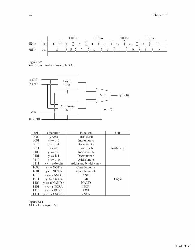
Figure 5.9Simulation results of example 5.4.
sel Operation Function Unit00000001001000110100010101100111
y <= ay <= a+1y <= a-1y <= b
y <= b+1y <= b-1y <= a+b
y <= a+b+cin
Transfer aIncrement aDecrement aTransfer b
Increment bDecrement bAdd a and b
Add a and b with carry
Arithmetic
10001001101010111100110111101111
y <= NOT ay <= NOT b
y <= a AND by <= a OR b
y <= a NAND by <= a NOR by <= a XOR b
y <= a XNOR b
Complement aComplement b
ANDOR
NANDNORXOR
XNOR
Logic
sel (3)
a (7:0)b (7:0)
cin
sel (3:0)
LogicUnit
ArithmeticUnit
Mux y (7:0)
Figure 5.10ALU of example 5.5.
76 Chapter 5
TLFeBOOK
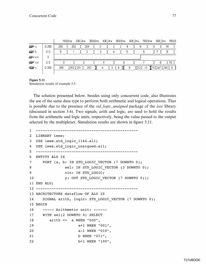
The solution presented below, besides using only concurrent code, also illustrates
the use of the same data type to perform both arithmetic and logical operations. That
is possible due to the presence of the std_logic_unsigned package of the ieee library
(discussed in section 3.6). Two signals, arith and logic, are used to hold the results
from the arithmetic and logic units, respectively, being the value passed to the output
selected by the multiplexer. Simulation results are shown in figure 5.11.
1 ----------------------------------------------
2 LIBRARY ieee;
3 USE ieee.std_logic_1164.all;
4 USE ieee.std_logic_unsigned.all;
5 ----------------------------------------------
6 ENTITY ALU IS
7 PORT (a, b: IN STD_LOGIC_VECTOR (7 DOWNTO 0);
8 sel: IN STD_LOGIC_VECTOR (3 DOWNTO 0);
9 cin: IN STD_LOGIC;
10 y: OUT STD_LOGIC_VECTOR (7 DOWNTO 0));
11 END ALU;
12 ----------------------------------------------
13 ARCHITECTURE dataflow OF ALU IS
14 SIGNAL arith, logic: STD_LOGIC_VECTOR (7 DOWNTO 0);
15 BEGIN
16 ----- Arithmetic unit: ------
17 WITH sel(2 DOWNTO 0) SELECT
18 arith <= a WHEN "000",
19 a+1 WHEN "001",
20 a-1 WHEN "010",
21 b WHEN "011",
22 b+1 WHEN "100",
Figure 5.11Simulation results of example 5.5.
Concurrent Code 77
TLFeBOOK
23 b-1 WHEN "101",
24 a+b WHEN "110",
25 a+b+cin WHEN OTHERS;
26 ----- Logic unit: -----------
27 WITH sel(2 DOWNTO 0) SELECT
28 logic <= NOT a WHEN "000",
29 NOT b WHEN "001",
30 a AND b WHEN "010",
31 a OR b WHEN "011",
32 a NAND b WHEN "100",
33 a NOR b WHEN "101",
34 a XOR b WHEN "110",
35 NOT (a XOR b) WHEN OTHERS;
36 -------- Mux: ---------------
37 WITH sel(3) SELECT
38 y <= arith WHEN '0',
39 logic WHEN OTHERS;
40 END dataflow;
41 ----------------------------------------------
5.4 GENERATE
GENERATE is another concurrent statement (along with operators and WHEN). It
is equivalent to the sequential statement LOOP (chapter 6) in the sense that it allows
a section of code to be repeated a number of times, thus creating several instances of
the same assignments. Its regular form is the FOR / GENERATE construct, with
the syntax shown below. Notice that GENERATE must be labeled.
FOR / GENERATE:
label: FOR identifier IN range GENERATE(concurrent assignments)
END GENERATE;
An irregular form is also available, which uses IF/GENERATE (with an IF
equivalent; recall that originally IF is a sequential statement). Here ELSE is not
allowed. In the same way that IF/GENERATE can be nested inside FOR/
GENERATE (syntax below), the opposite can also be done.
78 Chapter 5
TLFeBOOK
IF / GENERATE nested inside FOR / GENERATE:
label1: FOR identifier IN range GENERATE...label2: IF condition GENERATE
(concurrent assignments)END GENERATE;...
END GENERATE;
Example:
SIGNAL x: BIT_VECTOR (7 DOWNTO 0);
SIGNAL y: BIT_VECTOR (15 DOWNTO 0);
SIGNAL z: BIT_VECTOR (7 DOWNTO 0);
...
G1: FOR i IN x'RANGE GENERATE
z(i) <= x(i) AND y(i+8);
END GENERATE;
One important remark about GENERATE (and the same is true for LOOP,
which will be seen in chapter 6) is that both limits of the range must be static. As
an example, let us consider the code below, where choice is an input (non-static)
parameter. This kind of code is generally not synthesizable.
NotOK: FOR i IN 0 TO choice GENERATE
(concurrent statements)
END GENERATE;
We also must to be aware of multiply-driven (unresolved) signals. For example,
OK: FOR i IN 0 TO 7 GENERATE
output(i)<='1' WHEN (a(i) AND b(i))='1' ELSE '0';
END GENERATE;
is fine. However, the compiler will complain that accum is multiply driven (and stop
compilation) in either of the following two cases:
NotOK: FOR i IN 0 TO 7 GENERATE
accum <="11111111" WHEN (a(i) AND b(i))='1' ELSE "00000000";
END GENERATE;
Concurrent Code 79
TLFeBOOK
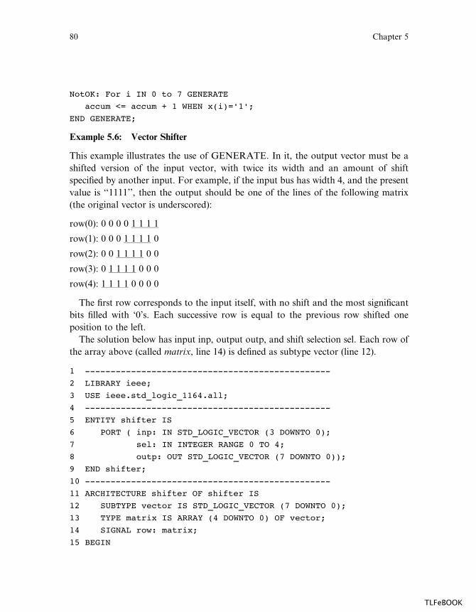
NotOK: For i IN 0 to 7 GENERATE
accum <= accum + 1 WHEN x(i)='1';
END GENERATE;
Example 5.6: Vector Shifter
This example illustrates the use of GENERATE. In it, the output vector must be a
shifted version of the input vector, with twice its width and an amount of shift
specified by another input. For example, if the input bus has width 4, and the present
value is ‘‘1111’’, then the output should be one of the lines of the following matrix
(the original vector is underscored):
row(0): 0 0 0 0 1 1 1 1
row(1): 0 0 0 1 1 1 1 0
row(2): 0 0 1 1 1 1 0 0
row(3): 0 1 1 1 1 0 0 0
row(4): 1 1 1 1 0 0 0 0
The first row corresponds to the input itself, with no shift and the most significant
bits filled with ‘0’s. Each successive row is equal to the previous row shifted one
position to the left.
The solution below has input inp, output outp, and shift selection sel. Each row of
the array above (called matrix, line 14) is defined as subtype vector (line 12).
1 ------------------------------------------------
2 LIBRARY ieee;
3 USE ieee.std_logic_1164.all;
4 ------------------------------------------------
5 ENTITY shifter IS
6 PORT ( inp: IN STD_LOGIC_VECTOR (3 DOWNTO 0);
7 sel: IN INTEGER RANGE 0 TO 4;
8 outp: OUT STD_LOGIC_VECTOR (7 DOWNTO 0));
9 END shifter;
10 ------------------------------------------------
11 ARCHITECTURE shifter OF shifter IS
12 SUBTYPE vector IS STD_LOGIC_VECTOR (7 DOWNTO 0);
13 TYPE matrix IS ARRAY (4 DOWNTO 0) OF vector;
14 SIGNAL row: matrix;
15 BEGIN
80 Chapter 5
TLFeBOOK

16 row(0) <= "0000" & inp;
17 G1: FOR i IN 1 TO 4 GENERATE
18 row(i) <= row(i-1)(6 DOWNTO 0) & '0';
19 END GENERATE;
20 outp <= row(sel);
21 END shifter;
22 ------------------------------------------------
Simulation results are presented in figure 5.12. As can be seen, inp ¼ ‘‘0011’’
(decimal 3) was applied to the circuit. The result was outp ¼ ‘‘00000011’’ (decimal 3)
when sel ¼ 0 (no shift), outp ¼ ‘‘00000110’’ (decimal 6) when sel ¼ 1 (one shift to the
left), outp ¼ ‘‘00001100’’ (decimal 12) when sel ¼ 2 (two shifts to the left), and so on.
5.5 BLOCK
There are two kinds of BLOCK statements: Simple and Guarded.
Simple BLOCK
The BLOCK statement, in its simple form, represents only a way of locally parti-
tioning the code. It allows a set of concurrent statements to be clustered into a
BLOCK, with the purpose of turning the overall code more readable and more
manageable (which might be helpful when dealing with long codes). Its syntax is
shown below.
label: BLOCK[declarative part]
BEGIN(concurrent statements)
END BLOCK label;
Figure 5.12Simulation results of example 5.6.
Concurrent Code 81
TLFeBOOK

Therefore, the overall aspect of a ‘‘blocked’’ code is the following:
------------------------
ARCHITECTURE example ...
BEGIN
...
block1: BLOCK
BEGIN
...
END BLOCK block1
...
block2: BLOCK
BEGIN
...
END BLOCK block2;
...
END example;
------------------------
Example:
b1: BLOCK
SIGNAL a: STD_LOGIC;
BEGIN
a <= input_sig WHEN ena='1' ELSE 'Z';
END BLOCK b1;
A BLOCK (simple or guarded) can be nested inside another BLOCK. The corre-
sponding syntax is shown below.
label1: BLOCK[declarative part of top block]
BEGIN[concurrent statements of top block]
label2: BLOCK[declarative part nested block]
BEGIN(concurrent statements of nested block)
END BLOCK label2;[more concurrent statements of top block]
END BLOCK label1;
82 Chapter 5
TLFeBOOK
Note: Although code partitioning techniques are the object of Part II of the book,
and the BLOCK statement seen above serves exactly to this purpose, BLOCK is
described in this section due to the fact that it is self-contained within the main code
(that is, it does not invoke any extra PACKAGE, COMPONENT, FUNCTION, or
PROCEDURE—these four units are the actual focus of Part II).
Guarded BLOCK
A guarded BLOCK is a special kind of BLOCK, which includes an additional ex-
pression, called guard expression. A guarded statement in a guarded BLOCK is exe-
cuted only when the guard expression is TRUE.
Guarded BLOCK:
label: BLOCK (guard expression)[declarative part]
BEGIN(concurrent guarded and unguarded statements)
END BLOCK label;
As the examples below illustrate, even though only concurrent statements can be
written within a BLOCK, with a guarded BLOCK even sequential circuits can be
constructed. This, however, is not a usual design approach.
Example 5.7: Latch Implemented with a Guarded BLOCK
The example presented below implements a transparent latch. In it, clk='1' (line
12) is the guard expression, while q<=GUARDED d (line 14) is a guarded statement.
Therefore, q<=d will only occur if clk='1'.
1 -------------------------------
2 LIBRARY ieee;
3 USE ieee.std_logic_1164.all;
4 -------------------------------
5 ENTITY latch IS
6 PORT (d, clk: IN STD_LOGIC;
7 q: OUT STD_LOGIC);
8 END latch;
9 -------------------------------
10 ARCHITECTURE latch OF latch IS
Concurrent Code 83
TLFeBOOK
11 BEGIN
12 b1: BLOCK (clk='1')
13 BEGIN
14 q <= GUARDED d;
15 END BLOCK b1;
16 END latch;
17 -------------------------------
Example 5.8: DFF Implemented with a Guarded BLOCK
Here, a positive-edge sensitive D-type flip-flop, with synchronous reset, is designed.
The interpretation of the code is similar to that in the example above. In it,
clk'EVENT AND clk='1' (line 12) is the guard expression, while q <= GUARDED '0'
WHEN rst='1' (line 14) is a guarded statement. Therefore, q<='0' will occur when
the guard expression is true and rst is ‘1’.
1 -------------------------------
2 LIBRARY ieee;
3 USE ieee.std_logic_1164.all;
4 -------------------------------
5 ENTITY dff IS
6 PORT ( d, clk, rst: IN STD_LOGIC;
7 q: OUT STD_LOGIC);
8 END dff;
9 -------------------------------
10 ARCHITECTURE dff OF dff IS
11 BEGIN
12 b1: BLOCK (clk'EVENT AND clk='1')
13 BEGIN
14 q <= GUARDED '0' WHEN rst='1' ELSE d;
15 END BLOCK b1;
16 END dff;
17 ------------------------------
5.6 Problems
The problems proposed in this section are to be solved using only concurrent code
(operators, WHEN, GENERATE). After writing the VHDL code, synthesize and
simulate it, to make sure that it works as expected.
84 Chapter 5
TLFeBOOK

Problem 5.1: Generic Multiplexer
We have seen the design of a multiplexer in examples 5.1 and 5.2. Those circuits were
for a pre-defined number of inputs (4 inputs) and a pre-defined number of bits per
input (1 bit). A truly generic mux is depicted in figure P5.1. In it, n represents the
number of bits of the selection input (sel), while m indicates the number of bits per
input. The circuit has 2n inputs (notice that there is no relationship between m and n).
Using a GENERIC statement to specify n, and assuming m ¼ 8, design this circuit.
Suggestion: The input should be specified as an array of vectors. Therefore, review
section 3.5. Does your solution (ARCHITECTURE) require more than one line of
actual code?
Problem 5.2: Priority Encoder
Figure P5.2 shows the top-level diagram of a 7-level priority encoder. The circuit
must encode the address of the input bit of highest order that is active. ‘‘000’’ should
indicate that there is no request at the input (no bit active). Write two solutions for
this circuit:
x(0)
x(1)
x(2n-1)
2n
sel
MUXm
m
n
y
Figure P5.1
‘0’‘1’‘0’‘0’‘1’’1’‘0’
7654321
PRIORITYENCODER
‘1’’1’‘0’
210
Figure P5.2
Concurrent Code 85
TLFeBOOK

(a) Using only operators;
(b) Using WHEN/ELSE (simple WHEN);
Problem 5.3: Simple Multiplier/Divider
Using only concurrent code, design the multiplier/divider of figure P5.3. The circuit
has two 8-bit integer inputs (a, b) and two integer outputs (x, y), where x ¼ a*b and
y ¼ a/2.
Note: For a generic fixed-point divider, you may consult chapter 9.
Problem 5.4: Adder
Using only concurrent statements, design the 8-bit unsigned adder of figure P5.4.
Problem 5.5: Signed/Unsigned Adder/Subtractor
In figure P5.5, we have added an extra 2-bit input (sel) to the circuit of problem 5.4,
such that now the circuit can operate as a signed or unsigned adder/subtractor (see
truth table). Write a concurrent VHDL code for this circuit.
Note: After having solved this problem, you can compare your solution to a corre-
sponding example in chapter 9.
a
b
x=a*b
y=a/2
*
/
Figure P5.3
a (7:0)
b (7:0)sum (7:0)
cin (carry in)
cout (carry out)
+
Figure P5.4
86 Chapter 5
TLFeBOOK

Problem 5.6: Binary-to-Gray Code Converter
Binary code is the most often used of all digital codes. In it, the LSB (least significant
bit) has weight 20, with the weight increasing by a factor of two for each successive
bit, up to 2n�1 for the MSB (most significant bit), where n is the number of bits in the
codeword. The Gray code, on the other hand, is based on minimum Hamming dis-
tance between neighboring codewords, that is, only one bit changes when we move
from the j-th to the ( jþ 1)-th codeword. Both codes, for n ¼ 4, are listed in table
P5.6. Design a circuit capable of converting binary code to Gray code (for generic n).
If possible, present more than one solution.
cout
a (7:0)
b (7:0)
sel (1:0)
sum (7:0)
cin
+
sel operation00011011
add unsignedadd signedsub unsignedsub signed
Figure P5.5
Table P5.6
Binary code Gray code
0000 0000
0001 0001
0010 0011
0011 0010
0100 0110
0101 0111
0110 0101
0111 0100
1000 1100
1001 1101
1010 1111
1011 1110
1100 1010
1101 1011
1110 1001
1111 1000
Concurrent Code 87
TLFeBOOK
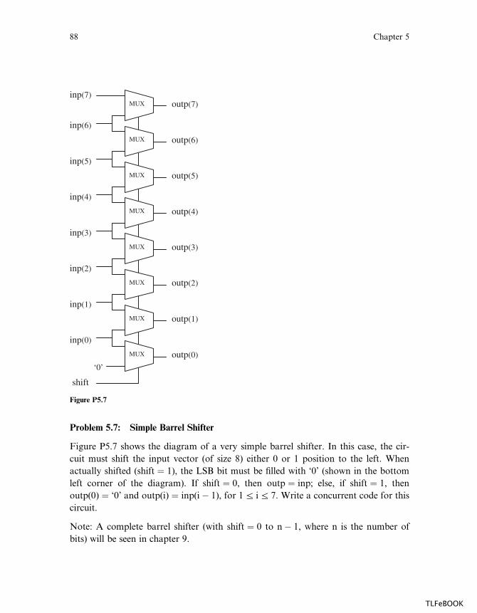
Problem 5.7: Simple Barrel Shifter
Figure P5.7 shows the diagram of a very simple barrel shifter. In this case, the cir-
cuit must shift the input vector (of size 8) either 0 or 1 position to the left. When
actually shifted (shift ¼ 1), the LSB bit must be filled with ‘0’ (shown in the bottom
left corner of the diagram). If shift ¼ 0, then outp ¼ inp; else, if shift ¼ 1, then
outp(0) ¼ ‘0’ and outp(i) ¼ inp(i� 1), for 1a ia 7. Write a concurrent code for this
circuit.
Note: A complete barrel shifter (with shift ¼ 0 to n� 1, where n is the number of
bits) will be seen in chapter 9.
shift
‘0’
outp(7)inp(7)
MUX
inp(6)
outp(6)MUX
inp(5)
outp(5)MUX
inp(4)
outp(4)MUX
inp(3)
outp(3)MUX
inp(2)
outp(2)MUX
inp(1)
outp(1)MUX
inp(0)
outp(0)MUX
Figure P5.7
88 Chapter 5
TLFeBOOK
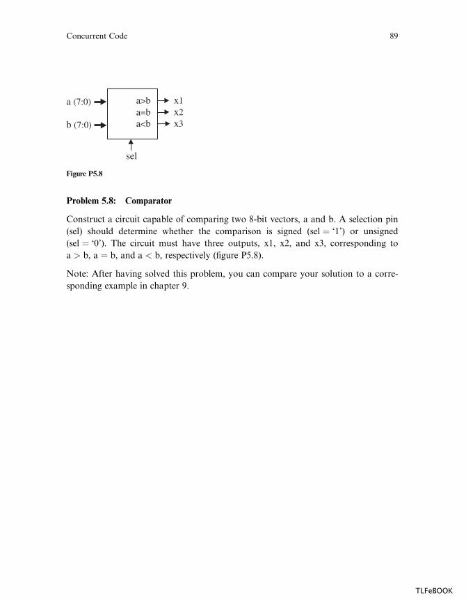
Problem 5.8: Comparator
Construct a circuit capable of comparing two 8-bit vectors, a and b. A selection pin
(sel) should determine whether the comparison is signed (sel ¼ ‘1’) or unsigned
(sel ¼ ‘0’). The circuit must have three outputs, x1, x2, and x3, corresponding to
a > b, a ¼ b, and a < b, respectively (figure P5.8).
Note: After having solved this problem, you can compare your solution to a corre-
sponding example in chapter 9.
a (7:0)
b (7:0)
x1x2x3
a>ba=ba<b
sel
Figure P5.8
Concurrent Code 89
TLFeBOOK

TLFeBOOK
6 Sequential Code
As mentioned in chapter 5, VHDL code is inherently concurrent. PROCESSES,
FUNCTIONS, and PROCEDURES are the only sections of code that are executed
sequentially. However, as a whole, any of these blocks is still concurrent with any
other statements placed outside it.
One important aspect of sequential code is that it is not limited to sequential logic.
Indeed, with it we can build sequential circuits as well as combinational circuits. Se-
quential code is also called behavioral code.
The statements discussed in this section are all sequential, that is, allowed only
inside PROCESSES, FUNCTIONS, or PROCEDURES. They are: IF, WAIT,
CASE, and LOOP.
VARIABLES are also restricted to be used in sequential code only (that is, inside
a PROCESS, FUNCTION, or PROCEDURE). Thus, contrary to a SIGNAL, a
VARIABLE can never be global, so its value can not be passed out directly.
We will concentrate on PROCESSES here. FUNCTIONS and PROCEDURES
are very similar, but are intended for system-level design, being therefore seen in Part
II of this book.
6.1 PROCESS
A PROCESS is a sequential section of VHDL code. It is characterized by the pres-
ence of IF, WAIT, CASE, or LOOP, and by a sensitivity list (except when WAIT is
used). A PROCESS must be installed in the main code, and is executed every time a
signal in the sensitivity list changes (or the condition related to WAIT is fulfilled). Its
syntax is shown below.
[label:] PROCESS (sensitivity list)[VARIABLE name type [range] [:= initial_value;]]
BEGIN(sequential code)
END PROCESS [label];
VARIABLES are optional. If used, they must be declared in the declarative part
of the PROCESS (before the word BEGIN, as indicated in the syntax above). The
initial value is not synthesizable, being only taken into consideration in simulations.
The use of a label is also optional. Its purpose is to improve code readability. The
label can be any word, except VHDL reserved words (appendix E).
TLFeBOOK
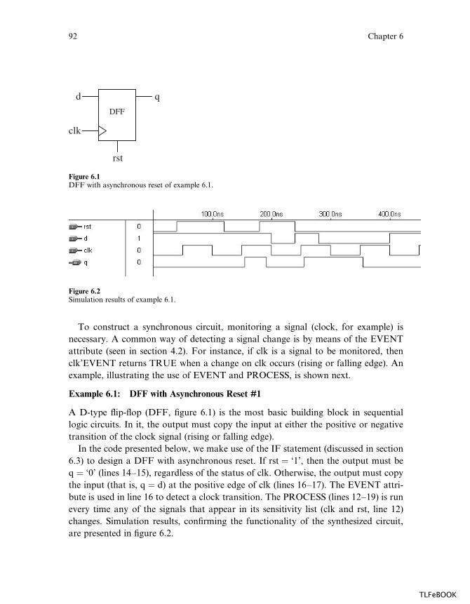
To construct a synchronous circuit, monitoring a signal (clock, for example) is
necessary. A common way of detecting a signal change is by means of the EVENT
attribute (seen in section 4.2). For instance, if clk is a signal to be monitored, then
clk’EVENT returns TRUE when a change on clk occurs (rising or falling edge). An
example, illustrating the use of EVENT and PROCESS, is shown next.
Example 6.1: DFF with Asynchronous Reset #1
A D-type flip-flop (DFF, figure 6.1) is the most basic building block in sequential
logic circuits. In it, the output must copy the input at either the positive or negative
transition of the clock signal (rising or falling edge).
In the code presented below, we make use of the IF statement (discussed in section
6.3) to design a DFF with asynchronous reset. If rst ¼ ‘1’, then the output must be
q ¼ ‘0’ (lines 14–15), regardless of the status of clk. Otherwise, the output must copy
the input (that is, q ¼ d) at the positive edge of clk (lines 16–17). The EVENT attri-
bute is used in line 16 to detect a clock transition. The PROCESS (lines 12–19) is run
every time any of the signals that appear in its sensitivity list (clk and rst, line 12)
changes. Simulation results, confirming the functionality of the synthesized circuit,
are presented in figure 6.2.
d
clk
q
DFF
rst
Figure 6.1DFF with asynchronous reset of example 6.1.
Figure 6.2Simulation results of example 6.1.
92 Chapter 6
TLFeBOOK
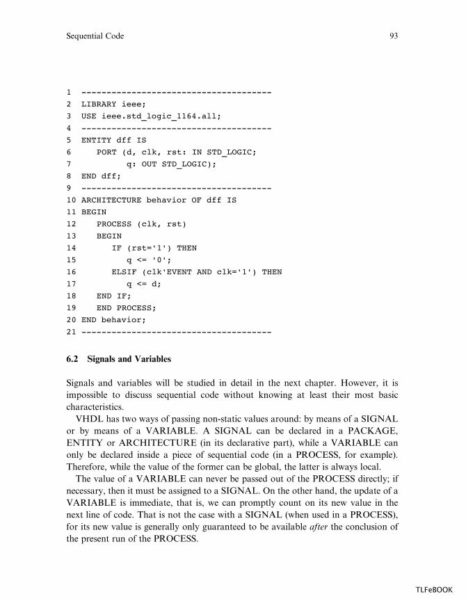
1 --------------------------------------
2 LIBRARY ieee;
3 USE ieee.std_logic_1164.all;
4 --------------------------------------
5 ENTITY dff IS
6 PORT (d, clk, rst: IN STD_LOGIC;
7 q: OUT STD_LOGIC);
8 END dff;
9 --------------------------------------
10 ARCHITECTURE behavior OF dff IS
11 BEGIN
12 PROCESS (clk, rst)
13 BEGIN
14 IF (rst='1') THEN
15 q <= '0';
16 ELSIF (clk'EVENT AND clk='1') THEN
17 q <= d;
18 END IF;
19 END PROCESS;
20 END behavior;
21 --------------------------------------
6.2 Signals and Variables
Signals and variables will be studied in detail in the next chapter. However, it is
impossible to discuss sequential code without knowing at least their most basic
characteristics.
VHDL has two ways of passing non-static values around: by means of a SIGNAL
or by means of a VARIABLE. A SIGNAL can be declared in a PACKAGE,
ENTITY or ARCHITECTURE (in its declarative part), while a VARIABLE can
only be declared inside a piece of sequential code (in a PROCESS, for example).
Therefore, while the value of the former can be global, the latter is always local.
The value of a VARIABLE can never be passed out of the PROCESS directly; if
necessary, then it must be assigned to a SIGNAL. On the other hand, the update of a
VARIABLE is immediate, that is, we can promptly count on its new value in the
next line of code. That is not the case with a SIGNAL (when used in a PROCESS),
for its new value is generally only guaranteed to be available after the conclusion of
the present run of the PROCESS.
Sequential Code 93
TLFeBOOK
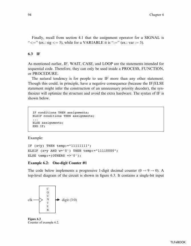
Finally, recall from section 4.1 that the assignment operator for a SIGNAL is
‘‘<¼’’ (ex.: sig <¼ 5), while for a VARIABLE it is ‘‘:¼’’ (ex.: var :¼ 5).
6.3 IF
As mentioned earlier, IF, WAIT, CASE, and LOOP are the statements intended for
sequential code. Therefore, they can only be used inside a PROCESS, FUNCTION,
or PROCEDURE.
The natural tendency is for people to use IF more than any other statement.
Though this could, in principle, have a negative consequence (because the IF/ELSE
statement might infer the construction of an unnecessary priority decoder), the syn-
thesizer will optimize the structure and avoid the extra hardware. The syntax of IF is
shown below.
IF conditions THEN assignments;ELSIF conditions THEN assignments;...ELSE assignments;END IF;
Example:
IF (x<y) THEN temp:="11111111";
ELSIF (x=y AND w='0') THEN temp:="11110000";
ELSE temp:=(OTHERS =>'0');
Example 6.2: One-digit Counter #1
The code below implements a progressive 1-digit decimal counter (0 ! 9 ! 0). A
top-level diagram of the circuit is shown in figure 6.3. It contains a single-bit input
clk digit (3:0)
COUNTER
Figure 6.3Counter of example 6.2.
94 Chapter 6
TLFeBOOK
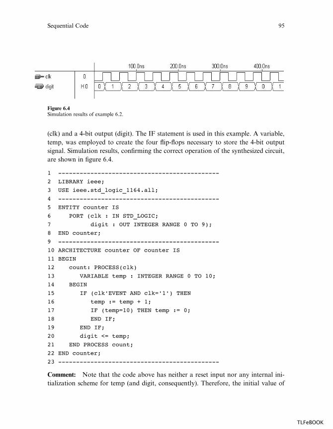
(clk) and a 4-bit output (digit). The IF statement is used in this example. A variable,
temp, was employed to create the four flip-flops necessary to store the 4-bit output
signal. Simulation results, confirming the correct operation of the synthesized circuit,
are shown in figure 6.4.
1 ---------------------------------------------
2 LIBRARY ieee;
3 USE ieee.std_logic_1164.all;
4 ---------------------------------------------
5 ENTITY counter IS
6 PORT (clk : IN STD_LOGIC;
7 digit : OUT INTEGER RANGE 0 TO 9);
8 END counter;
9 ---------------------------------------------
10 ARCHITECTURE counter OF counter IS
11 BEGIN
12 count: PROCESS(clk)
13 VARIABLE temp : INTEGER RANGE 0 TO 10;
14 BEGIN
15 IF (clk'EVENT AND clk='1') THEN
16 temp := temp + 1;
17 IF (temp=10) THEN temp := 0;
18 END IF;
19 END IF;
20 digit <= temp;
21 END PROCESS count;
22 END counter;
23 ---------------------------------------------
Comment: Note that the code above has neither a reset input nor any internal ini-
tialization scheme for temp (and digit, consequently). Therefore, the initial value of
Figure 6.4Simulation results of example 6.2.
Sequential Code 95
TLFeBOOK
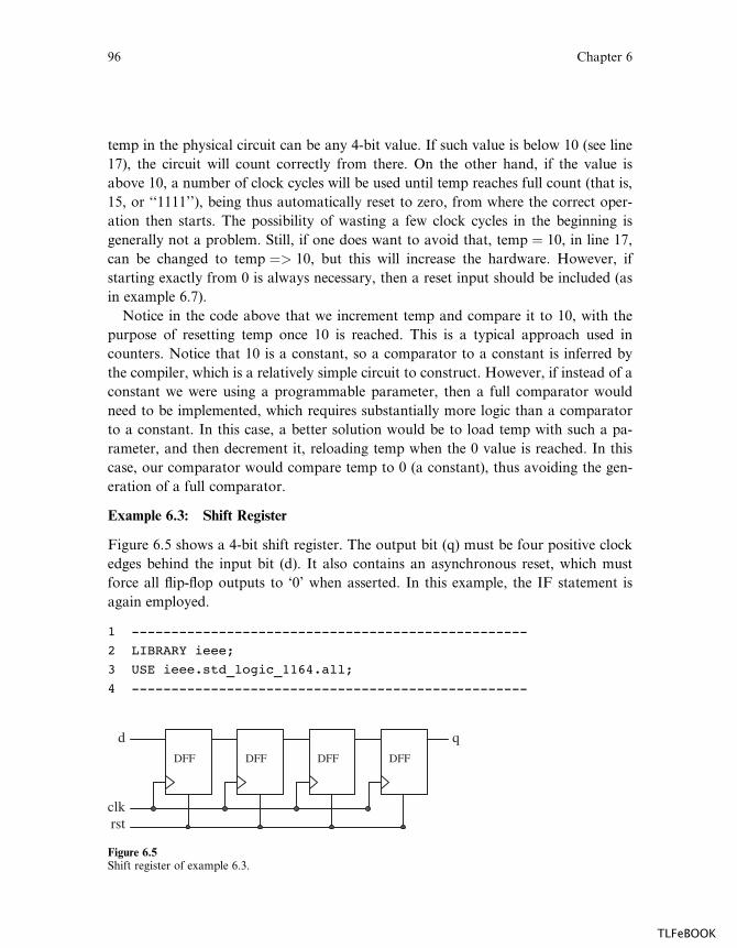
temp in the physical circuit can be any 4-bit value. If such value is below 10 (see line
17), the circuit will count correctly from there. On the other hand, if the value is
above 10, a number of clock cycles will be used until temp reaches full count (that is,
15, or ‘‘1111’’), being thus automatically reset to zero, from where the correct oper-
ation then starts. The possibility of wasting a few clock cycles in the beginning is
generally not a problem. Still, if one does want to avoid that, temp ¼ 10, in line 17,
can be changed to temp ¼> 10, but this will increase the hardware. However, if
starting exactly from 0 is always necessary, then a reset input should be included (as
in example 6.7).
Notice in the code above that we increment temp and compare it to 10, with the
purpose of resetting temp once 10 is reached. This is a typical approach used in
counters. Notice that 10 is a constant, so a comparator to a constant is inferred by
the compiler, which is a relatively simple circuit to construct. However, if instead of a
constant we were using a programmable parameter, then a full comparator would
need to be implemented, which requires substantially more logic than a comparator
to a constant. In this case, a better solution would be to load temp with such a pa-
rameter, and then decrement it, reloading temp when the 0 value is reached. In this
case, our comparator would compare temp to 0 (a constant), thus avoiding the gen-
eration of a full comparator.
Example 6.3: Shift Register
Figure 6.5 shows a 4-bit shift register. The output bit (q) must be four positive clock
edges behind the input bit (d). It also contains an asynchronous reset, which must
force all flip-flop outputs to ‘0’ when asserted. In this example, the IF statement is
again employed.
1 --------------------------------------------------
2 LIBRARY ieee;
3 USE ieee.std_logic_1164.all;
4 --------------------------------------------------
d
clkrst
q
DFF DFF DFF DFF
Figure 6.5Shift register of example 6.3.
96 Chapter 6
TLFeBOOK
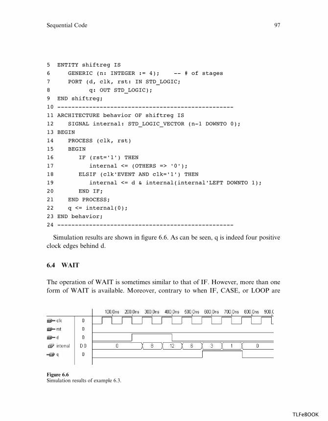
5 ENTITY shiftreg IS
6 GENERIC (n: INTEGER := 4); -- # of stages
7 PORT (d, clk, rst: IN STD_LOGIC;
8 q: OUT STD_LOGIC);
9 END shiftreg;
10 --------------------------------------------------
11 ARCHITECTURE behavior OF shiftreg IS
12 SIGNAL internal: STD_LOGIC_VECTOR (n-1 DOWNTO 0);
13 BEGIN
14 PROCESS (clk, rst)
15 BEGIN
16 IF (rst='1') THEN
17 internal <= (OTHERS => '0');
18 ELSIF (clk'EVENT AND clk='1') THEN
19 internal <= d & internal(internal'LEFT DOWNTO 1);
20 END IF;
21 END PROCESS;
22 q <= internal(0);
23 END behavior;
24 --------------------------------------------------
Simulation results are shown in figure 6.6. As can be seen, q is indeed four positive
clock edges behind d.
6.4 WAIT
The operation of WAIT is sometimes similar to that of IF. However, more than one
form of WAIT is available. Moreover, contrary to when IF, CASE, or LOOP are
Figure 6.6Simulation results of example 6.3.
Sequential Code 97
TLFeBOOK

used, the PROCESS cannot have a sensitivity list when WAIT is employed. Its syntax
(there are three forms of WAIT) is shown below.
WAIT UNTIL signal_condition;
WAIT ON signal1 [, signal2, ... ];
WAIT FOR time;
The WAIT UNTIL statement accepts only one signal, thus being more appropri-
ate for synchronous code than asynchronous. Since the PROCESS has no sensitivity
list in this case, WAIT UNTIL must be the first statement in the PROCESS. The
PROCESS will be executed every time the condition is met.
Example: 8-bit register with synchronous reset.
PROCESS -- no sensitivity list
BEGIN
WAIT UNTIL (clk'EVENT AND clk='1');
IF (rst='1') THEN
output <= "00000000";
ELSIF (clk'EVENT AND clk='1') THEN
output <= input;
END IF;
END PROCESS;
WAIT ON, on the other hand, accepts multiple signals. The PROCESS is put on
hold until any of the signals listed changes. In the example below, the PROCESS will
continue execution whenever a change in rst or clk occurs.
Example: 8-bit register with asynchronous reset.
PROCESS
BEGIN
WAIT ON clk, rst;
IF (rst='1') THEN
98 Chapter 6
TLFeBOOK
output <= "00000000";
ELSIF (clk'EVENT AND clk='1') THEN
output <= input;
END IF;
END PROCESS;
Finally, WAIT FOR is intended for simulation only (waveform generation for
testbenches). Example: WAIT FOR 5ns;
Example 6.4: DFF with Asynchronous Reset #2
The code below implements the same DFF of example 6.1 (figures 6.1 and 6.2).
However, here WAIT ON is used instead of IF only.
1 --------------------------------------
2 LIBRARY ieee;
3 USE ieee.std_logic_1164.all;
4 --------------------------------------
5 ENTITY dff IS
6 PORT (d, clk, rst: IN STD_LOGIC;
7 q: OUT STD_LOGIC);
8 END dff;
9 --------------------------------------
10 ARCHITECTURE dff OF dff IS
11 BEGIN
12 PROCESS
13 BEGIN
14 WAIT ON rst, clk;
15 IF (rst='1') THEN
16 q <= '0';
17 ELSIF (clk'EVENT AND clk='1') THEN
18 q <= d;
19 END IF;
20 END PROCESS;
21 END dff;
22 --------------------------------------
Example 6.5: One-digit Counter #2
The code below implements the same progressive 1-digit decimal counter of example
6.2 (figures 6.3 and 6.4). However, WAIT UNTIL was used instead of IF only.
Sequential Code 99
TLFeBOOK
1 ---------------------------------------------
2 LIBRARY ieee;
3 USE ieee.std_logic_1164.all;
4 ---------------------------------------------
5 ENTITY counter IS
6 PORT (clk : IN STD_LOGIC;
7 digit : OUT INTEGER RANGE 0 TO 9);
8 END counter;
9 ---------------------------------------------
10 ARCHITECTURE counter OF counter IS
11 BEGIN
12 PROCESS -- no sensitivity list
13 VARIABLE temp : INTEGER RANGE 0 TO 10;
14 BEGIN
15 WAIT UNTIL (clk'EVENT AND clk='1');
16 temp := temp + 1;
17 IF (temp=10) THEN temp := 0;
18 END IF;
19 digit <= temp;
20 END PROCESS;
21 END counter;
22 ---------------------------------------------
6.5 CASE
CASE is another statement intended exclusively for sequential code (along with IF,
LOOP, and WAIT). Its syntax is shown below.
CASE identifier ISWHEN value => assignments;WHEN value => assignments;...
END CASE;
Example:
CASE control IS
WHEN "00" => x<=a; y<=b;
100 Chapter 6
TLFeBOOK

WHEN "01" => x<=b; y<=c;
WHEN OTHERS => x<="0000"; y<="ZZZZ";
END CASE;
The CASE statement (sequential) is very similar to WHEN (combinational). Here
too all permutations must be tested, so the keyword OTHERS is often helpful.
Another important keyword is NULL (the counterpart of UNAFFECTED), which
should be used when no action is to take place. For example, WHEN OTHERS =>
NULL;. However, CASE allows multiple assignments for each test condition (as
shown in the example above), while WHEN allows only one.
Like in the case of WHEN (section 5.3), here too ‘‘WHEN value’’ can take up
three forms:
WHEN value -- single value
WHEN value1 to value2 -- range, for enumerated data types
-- only
WHEN value1 | value2 |... -- value1 or value2 or ...
Example 6.6: DFF with Asynchronous Reset #3
The code below implements the same DFF of example 6.1 (figures 6.1 and 6.2).
However, here CASE was used instead of IF only. Notice that a few unnecessary
declarations were intentionally included in the code to illustrate their usage.
1 ----------------------------------------------
2 LIBRARY ieee; -- Unnecessary declaration,
3 -- because
4 USE ieee.std_logic_1164.all; -- BIT was used instead of
5 -- STD_LOGIC
6 ----------------------------------------------
7 ENTITY dff IS
8 PORT (d, clk, rst: IN BIT;
9 q: OUT BIT);
10 END dff;
11 ----------------------------------------------
12 ARCHITECTURE dff3 OF dff IS
13 BEGIN
14 PROCESS (clk, rst)
15 BEGIN
16 CASE rst IS
Sequential Code 101
TLFeBOOK
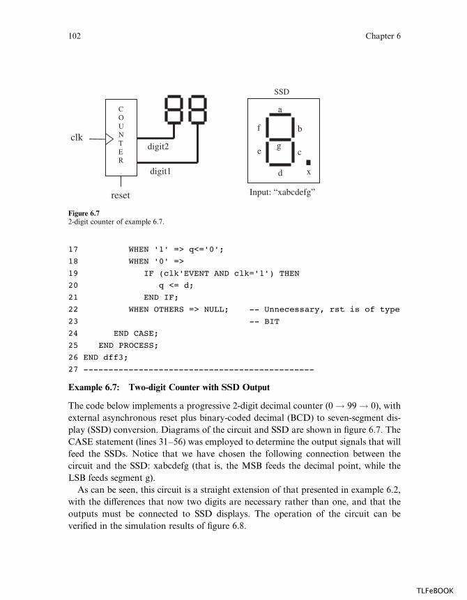
17 WHEN '1' => q<='0';
18 WHEN '0' =>
19 IF (clk'EVENT AND clk='1') THEN
20 q <= d;
21 END IF;
22 WHEN OTHERS => NULL; -- Unnecessary, rst is of type
23 -- BIT
24 END CASE;
25 END PROCESS;
26 END dff3;
27 ----------------------------------------------
Example 6.7: Two-digit Counter with SSD Output
The code below implements a progressive 2-digit decimal counter (0 ! 99 ! 0), with
external asynchronous reset plus binary-coded decimal (BCD) to seven-segment dis-
play (SSD) conversion. Diagrams of the circuit and SSD are shown in figure 6.7. The
CASE statement (lines 31–56) was employed to determine the output signals that will
feed the SSDs. Notice that we have chosen the following connection between the
circuit and the SSD: xabcdefg (that is, the MSB feeds the decimal point, while the
LSB feeds segment g).
As can be seen, this circuit is a straight extension of that presented in example 6.2,
with the di¤erences that now two digits are necessary rather than one, and that the
outputs must be connected to SSD displays. The operation of the circuit can be
verified in the simulation results of figure 6.8.
digit2
digit1
clk
COUNTER
reset
SSD
e
f
a
b
c
d
g
x
Input: “xabcdefg”
Figure 6.72-digit counter of example 6.7.
102 Chapter 6
TLFeBOOK

1 --------------------------------------------------
2 LIBRARY ieee;
3 USE ieee.std_logic_1164.all;
4 --------------------------------------------------
5 ENTITY counter IS
6 PORT (clk, reset : IN STD_LOGIC;
7 digit1, digit2 : OUT STD_LOGIC_VECTOR (6 DOWNTO 0));
8 END counter;
9 --------------------------------------------------
10 ARCHITECTURE counter OF counter IS
11 BEGIN
12 PROCESS(clk, reset)
13 VARIABLE temp1: INTEGER RANGE 0 TO 10;
14 VARIABLE temp2: INTEGER RANGE 0 TO 10;
15 BEGIN
16 ---- counter: ----------------------
17 IF (reset='1') THEN
18 temp1 := 0;
19 temp2 := 0;
20 ELSIF (clk'EVENT AND clk='1') THEN
21 temp1 := temp1 + 1;
22 IF (temp1=10) THEN
23 temp1 := 0;
24 temp2 := temp2 + 1;
25 IF (temp2=10) THEN
26 temp2 := 0;
Figure 6.8Simulation results of example 6.7.
Sequential Code 103
TLFeBOOK
27 END IF;
28 END IF;
29 END IF;
30 ---- BCD to SSD conversion: --------
31 CASE temp1 IS
32 WHEN 0 => digit1 <= "1111110"; --7E
33 WHEN 1 => digit1 <= "0110000"; --30
34 WHEN 2 => digit1 <= "1101101"; --6D
35 WHEN 3 => digit1 <= "1111001"; --79
36 WHEN 4 => digit1 <= "0110011"; --33
37 WHEN 5 => digit1 <= "1011011"; --5B
38 WHEN 6 => digit1 <= "1011111"; --5F
39 WHEN 7 => digit1 <= "1110000"; --70
40 WHEN 8 => digit1 <= "1111111"; --7F
41 WHEN 9 => digit1 <= "1111011"; --7B
42 WHEN OTHERS => NULL;
43 END CASE;
44 CASE temp2 IS
45 WHEN 0 => digit2 <= "1111110"; --7E
46 WHEN 1 => digit2 <= "0110000"; --30
47 WHEN 2 => digit2 <= "1101101"; --6D
48 WHEN 3 => digit2 <= "1111001"; --79
49 WHEN 4 => digit2 <= "0110011"; --33
50 WHEN 5 => digit2 <= "1011011"; --5B
51 WHEN 6 => digit2 <= "1011111"; --5F
52 WHEN 7 => digit2 <= "1110000"; --70
53 WHEN 8 => digit2 <= "1111111"; --7F
54 WHEN 9 => digit2 <= "1111011"; --7B
55 WHEN OTHERS => NULL;
56 END CASE;
57 END PROCESS;
58 END counter;
59 --------------------------------------------------
Comment: Notice above that the same routine was repeated twice (using CASE
statements). We will learn, in Part II, how to write and compile frequently used
pieces of code into user-defined libraries, so that such repetitions can be avoided.
104 Chapter 6
TLFeBOOK

6.6 LOOP
As the name says, LOOP is useful when a piece of code must be instantiated several
times. Like IF, WAIT, and CASE, LOOP is intended exclusively for sequential code,
so it too can only be used inside a PROCESS, FUNCTION, or PROCEDURE.
There are several ways of using LOOP, as shown in the syntaxes below.
FOR / LOOP: The loop is repeated a fixed number of times.
[label:] FOR identifier IN range LOOP(sequential statements)
END LOOP [label];
WHILE / LOOP: The loop is repeated until a condition no longer holds.
[label:] WHILE condition LOOP(sequential statements)
END LOOP [label];
EXIT: Used for ending the loop.
[label:] EXIT [label] [WHEN condition];
NEXT: Used for skipping loop steps.
[label:] NEXT [loop_label] [WHEN condition];
Example of FOR / LOOP:
FOR i IN 0 TO 5 LOOP
x(i) <= enable AND w(i+2);
y(0, i) <= w(i);
END LOOP;
In the code above, the loop will be repeated unconditionally until i reaches 5 (that
is, six times).
Sequential Code 105
TLFeBOOK
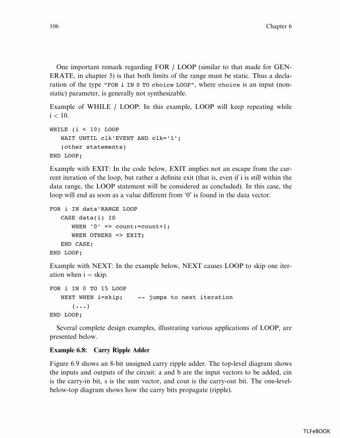
One important remark regarding FOR / LOOP (similar to that made for GEN-
ERATE, in chapter 5) is that both limits of the range must be static. Thus a decla-
ration of the type "FOR i IN 0 TO choice LOOP", where choice is an input (non-
static) parameter, is generally not synthesizable.
Example of WHILE / LOOP: In this example, LOOP will keep repeating while
i < 10.
WHILE (i < 10) LOOP
WAIT UNTIL clk'EVENT AND clk='1';
(other statements)
END LOOP;
Example with EXIT: In the code below, EXIT implies not an escape from the cur-
rent iteration of the loop, but rather a definite exit (that is, even if i is still within the
data range, the LOOP statement will be considered as concluded). In this case, the
loop will end as soon as a value di¤erent from ‘0’ is found in the data vector.
FOR i IN data'RANGE LOOP
CASE data(i) IS
WHEN '0' => count:=count+1;
WHEN OTHERS => EXIT;
END CASE;
END LOOP;
Example with NEXT: In the example below, NEXT causes LOOP to skip one iter-
ation when i ¼ skip.
FOR i IN 0 TO 15 LOOP
NEXT WHEN i=skip; -- jumps to next iteration
(...)
END LOOP;
Several complete design examples, illustrating various applications of LOOP, are
presented below.
Example 6.8: Carry Ripple Adder
Figure 6.9 shows an 8-bit unsigned carry ripple adder. The top-level diagram shows
the inputs and outputs of the circuit: a and b are the input vectors to be added, cin
is the carry-in bit, s is the sum vector, and cout is the carry-out bit. The one-level-
below-top diagram shows how the carry bits propagate (ripple).
106 Chapter 6
TLFeBOOK
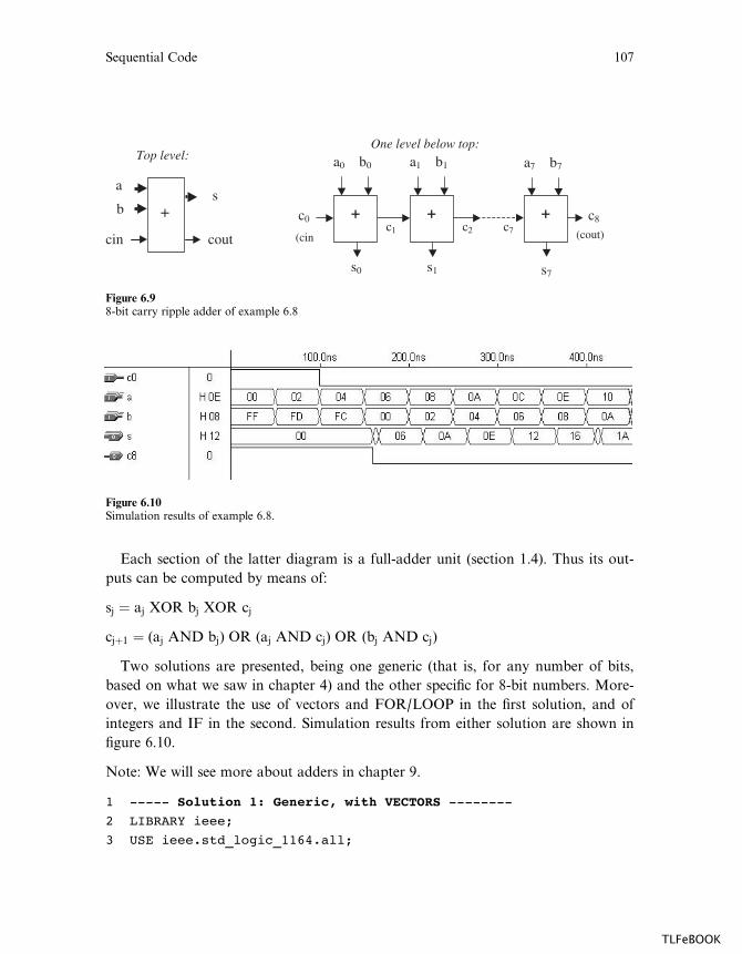
Each section of the latter diagram is a full-adder unit (section 1.4). Thus its out-
puts can be computed by means of:
sj ¼ aj XOR bj XOR cj
cjþ1 ¼ (aj AND bj) OR (aj AND cj) OR (bj AND cj)
Two solutions are presented, being one generic (that is, for any number of bits,
based on what we saw in chapter 4) and the other specific for 8-bit numbers. More-
over, we illustrate the use of vectors and FOR/LOOP in the first solution, and of
integers and IF in the second. Simulation results from either solution are shown in
figure 6.10.
Note: We will see more about adders in chapter 9.
1 ----- Solution 1: Generic, with VECTORS --------
2 LIBRARY ieee;
3 USE ieee.std_logic_1164.all;
c0 c8c7c1
s0
a0 b0
+c2
s1
a1 b1
+
s7
a7 b7
+
(cin (cout)
One level below top:Top level:
a
b
cin
s
cout
+
Figure 6.98-bit carry ripple adder of example 6.8
Figure 6.10Simulation results of example 6.8.
Sequential Code 107
TLFeBOOK
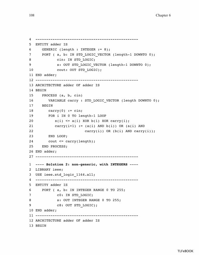
4 ------------------------------------------------
5 ENTITY adder IS
6 GENERIC (length : INTEGER := 8);
7 PORT ( a, b: IN STD_LOGIC_VECTOR (length-1 DOWNTO 0);
8 cin: IN STD_LOGIC;
9 s: OUT STD_LOGIC_VECTOR (length-1 DOWNTO 0);
10 cout: OUT STD_LOGIC);
11 END adder;
12 ------------------------------------------------
13 ARCHITECTURE adder OF adder IS
14 BEGIN
15 PROCESS (a, b, cin)
16 VARIABLE carry : STD_LOGIC_VECTOR (length DOWNTO 0);
17 BEGIN
18 carry(0) := cin;
19 FOR i IN 0 TO length-1 LOOP
20 s(i) <= a(i) XOR b(i) XOR carry(i);
21 carry(i+1) := (a(i) AND b(i)) OR (a(i) AND
22 carry(i)) OR (b(i) AND carry(i));
23 END LOOP;
24 cout <= carry(length);
25 END PROCESS;
26 END adder;
27 ------------------------------------------------
1 ---- Solution 2: non-generic, with INTEGERS ----
2 LIBRARY ieee;
3 USE ieee.std_logic_1164.all;
4 ------------------------------------------------
5 ENTITY adder IS
6 PORT ( a, b: IN INTEGER RANGE 0 TO 255;
7 c0: IN STD_LOGIC;
8 s: OUT INTEGER RANGE 0 TO 255;
9 c8: OUT STD_LOGIC);
10 END adder;
11 ------------------------------------------------
12 ARCHITECTURE adder OF adder IS
13 BEGIN
108 Chapter 6
TLFeBOOK
14 PROCESS (a, b, c0)
15 VARIABLE temp : INTEGER RANGE 0 TO 511;
16 BEGIN
17 IF (c0='1') THEN temp:=1;
18 ELSE temp:=0;
19 END IF;
20 temp := a + b + temp;
21 IF (temp > 255) THEN
22 c8 <= '1';
23 temp := temp---256;
24 ELSE c8 <= '0';
25 END IF;
26 s <= temp;
27 END PROCESS;
28 END adder;
29 ------------------------------------------------
Example 6.9: Simple Barrel Shifter
Figure 6.11 shows the diagram of a very simple barrel shifter. In this case, the circuit
must shift the input vector (of size 8) either 0 or 1 position to the left. When actually
shifted (shift ¼ 1), the LSB bit must be filled with ‘0’ (shown in the botton left corner
of the diagram). If shift ¼ 0, then outp ¼ inp; if shift ¼ 1, then outp(0) ¼ ‘0’ and
outp(i) ¼ inp(i� 1), for 1a ia 7.
A complete VHDL code is presented below, which illustrates the use of FOR/
LOOP. Simulation results appear in figure 6.12.
Note: A complete barrel shifter (with shift ¼ 0 to n� 1, where n is the size of the
input vector) will be seen in chapter 9.
1 ---------------------------------------------
2 LIBRARY ieee;
3 USE ieee.std_logic_1164.all;
4 ---------------------------------------------
5 ENTITY barrel IS
6 GENERIC (n: INTEGER := 8);
7 PORT ( inp: IN STD_LOGIC_VECTOR (n-1 DOWNTO 0);
8 shift: IN INTEGER RANGE 0 TO 1;
9 outp: OUT STD_LOGIC_VECTOR (n-1 DOWNTO 0));
Sequential Code 109
TLFeBOOK

shift
‘0’
outp(7)inp(7)
MUX
inp(6)
outp(6)MUX
inp(5)
outp(5)MUX
inp(4)
outp(4)MUX
inp(3)
outp(3)MUX
inp(2)
outp(2)MUX
inp(1)
outp(1)MUX
inp(0)
outp(0)MUX
Figure 6.11Simple barrel shifter of example 6.9.
Figure 6.12Simulation results of example 6.9.
110 Chapter 6
TLFeBOOK
10 END barrel;
11 ---------------------------------------------
12 ARCHITECTURE RTL OF barrel IS
13 BEGIN
14 PROCESS (inp, shift)
15 BEGIN
16 IF (shift=0) THEN
17 outp <= inp;
18 ELSE
19 outp(0) <= '0';
20 FOR i IN 1 TO inp'HIGH LOOP
21 outp(i) <= inp(i-1);
22 END LOOP;
23 END IF;
24 END PROCESS;
25 END RTL;
26 ---------------------------------------------
Example 6.10: Leading Zeros
The design below counts the number of leading zeros in a binary vector, starting
from the left end. The solution illustrates the use of LOOP / EXIT. Recall that EXIT
implies not a escape from the current iteration of the loop, but rather a definite exit
from it (that is, even if i is still within the specified range, the LOOP statement will be
considered as concluded). In this example, the loop will end as soon as a ‘1’ is found
in the data vector. Therefore, it is appropriate for counting the number of zeros that
precedes the first one.
1 --------------------------------------------
2 LIBRARY ieee;
3 USE ieee.std_logic_1164.all;
4 --------------------------------------------
5 ENTITY LeadingZeros IS
6 PORT ( data: IN STD_LOGIC_VECTOR (7 DOWNTO 0);
7 zeros: OUT INTEGER RANGE 0 TO 8);
8 END LeadingZeros;
9 --------------------------------------------
10 ARCHITECTURE behavior OF LeadingZeros IS
Sequential Code 111
TLFeBOOK
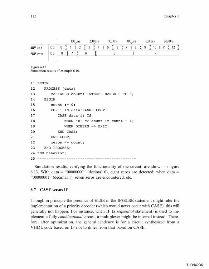
11 BEGIN
12 PROCESS (data)
13 VARIABLE count: INTEGER RANGE 0 TO 8;
14 BEGIN
15 count := 0;
16 FOR i IN data'RANGE LOOP
17 CASE data(i) IS
18 WHEN '0' => count := count + 1;
19 WHEN OTHERS => EXIT;
20 END CASE;
21 END LOOP;
22 zeros <= count;
23 END PROCESS;
24 END behavior;
25 --------------------------------------------
Simulation results, verifying the functionality of the circuit, are shown in figure
6.13. With data ¼ ‘‘00000000’’ (decimal 0), eight zeros are detected; when data ¼‘‘00000001’’ (decimal 1), seven zeros are encountered; etc.
6.7 CASE versus IF
Though in principle the presence of ELSE in the IF/ELSE statement might infer the
implementation of a priority decoder (which would never occur with CASE), this will
generally not happen. For instance, when IF (a sequential statement) is used to im-
plement a fully combinational circuit, a multiplexer might be inferred instead. There-
fore, after optimization, the general tendency is for a circuit synthesized from a
VHDL code based on IF not to di¤er from that based on CASE.
Figure 6.13Simulation results of example 6.10.
112 Chapter 6
TLFeBOOK
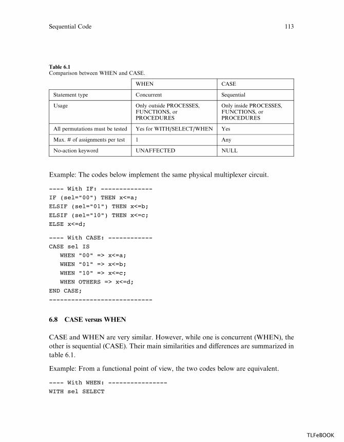
Example: The codes below implement the same physical multiplexer circuit.
---- With IF: --------------
IF (sel="00") THEN x<=a;
ELSIF (sel="01") THEN x<=b;
ELSIF (sel="10") THEN x<=c;
ELSE x<=d;
---- With CASE: ------------
CASE sel IS
WHEN "00" => x<=a;
WHEN "01" => x<=b;
WHEN "10" => x<=c;
WHEN OTHERS => x<=d;
END CASE;
----------------------------
6.8 CASE versus WHEN
CASE and WHEN are very similar. However, while one is concurrent (WHEN), the
other is sequential (CASE). Their main similarities and di¤erences are summarized in
table 6.1.
Example: From a functional point of view, the two codes below are equivalent.
---- With WHEN: ----------------
WITH sel SELECT
Table 6.1Comparison between WHEN and CASE.
WHEN CASE
Statement type Concurrent Sequential
Usage Only outside PROCESSES,FUNCTIONS, orPROCEDURES
Only inside PROCESSES,FUNCTIONS, orPROCEDURES
All permutations must be tested Yes for WITH/SELECT/WHEN Yes
Max. # of assignments per test 1 Any
No-action keyword UNAFFECTED NULL
Sequential Code 113
TLFeBOOK
x <= a WHEN "000",
b WHEN "001",
c WHEN "010",
UNAFFECTED WHEN OTHERS;
---- With CASE: ----------------
CASE sel IS
WHEN "000" => x<=a;
WHEN "001" => x<=b;
WHEN "010" => x<=c;
WHEN OTHERS => NULL;
END CASE;
--------------------------------
6.9 Bad Clocking
The compiler will generally not be able to synthesize codes that contain assignments
to the same signal at both transitions of the reference (clock) signal (that is, at the
rising edge plus at the falling edge). This is particularly true when the target tech-
nology contains only single-edge flip-flops (CPLDs, for example—appendix A). In
this case, the compiler might display a message of the type ‘‘signal does not hold
value after clock edge’’ or similar.
As an example, let us consider the case of a counter that must be incremented
at every clock transition (rising plus falling edge). One alternative could be the
following:
PROCESS (clk)
BEGIN
IF(clk'EVENT AND clk='1') THEN
counter <= counter + 1;
ELSIF(clk'EVENT AND clk='0') THEN
counter <= counter + 1;
END IF;
...
END PROCESS;
In this case, besides the messages already described, the compiler might also com-
plain that the signal counter is multiply driven. In any case, compilation will be
suspended.
114 Chapter 6
TLFeBOOK
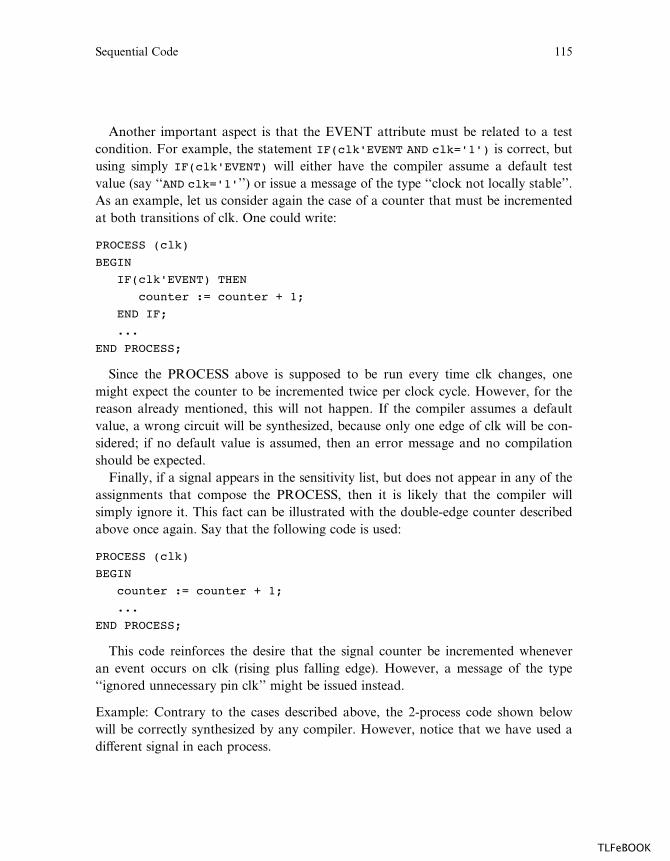
Another important aspect is that the EVENT attribute must be related to a test
condition. For example, the statement IF(clk'EVENT AND clk='1') is correct, but
using simply IF(clk'EVENT) will either have the compiler assume a default test
value (say ‘‘AND clk='1'’’) or issue a message of the type ‘‘clock not locally stable’’.
As an example, let us consider again the case of a counter that must be incremented
at both transitions of clk. One could write:
PROCESS (clk)
BEGIN
IF(clk'EVENT) THEN
counter := counter + 1;
END IF;
...
END PROCESS;
Since the PROCESS above is supposed to be run every time clk changes, one
might expect the counter to be incremented twice per clock cycle. However, for the
reason already mentioned, this will not happen. If the compiler assumes a default
value, a wrong circuit will be synthesized, because only one edge of clk will be con-
sidered; if no default value is assumed, then an error message and no compilation
should be expected.
Finally, if a signal appears in the sensitivity list, but does not appear in any of the
assignments that compose the PROCESS, then it is likely that the compiler will
simply ignore it. This fact can be illustrated with the double-edge counter described
above once again. Say that the following code is used:
PROCESS (clk)
BEGIN
counter := counter + 1;
...
END PROCESS;
This code reinforces the desire that the signal counter be incremented whenever
an event occurs on clk (rising plus falling edge). However, a message of the type
‘‘ignored unnecessary pin clk’’ might be issued instead.
Example: Contrary to the cases described above, the 2-process code shown below
will be correctly synthesized by any compiler. However, notice that we have used a
di¤erent signal in each process.
Sequential Code 115
TLFeBOOK
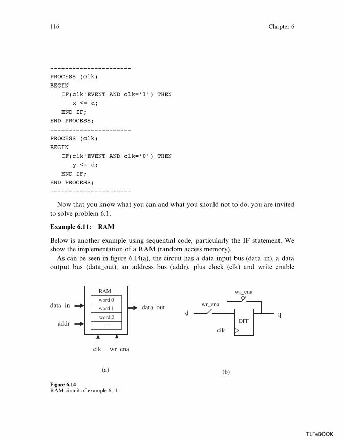
----------------------
PROCESS (clk)
BEGIN
IF(clk'EVENT AND clk='1') THEN
x <= d;
END IF;
END PROCESS;
----------------------
PROCESS (clk)
BEGIN
IF(clk'EVENT AND clk='0') THEN
y <= d;
END IF;
END PROCESS;
----------------------
Now that you know what you can and what you should not to do, you are invited
to solve problem 6.1.
Example 6.11: RAM
Below is another example using sequential code, particularly the IF statement. We
show the implementation of a RAM (random access memory).
As can be seen in figure 6.14(a), the circuit has a data input bus (data_in), a data
output bus (data_out), an address bus (addr), plus clock (clk) and write enable
(a) (b)
data in data_out
RAM
word 0
word 1
word 2
…
clk wr ena
addrclk
DFF
d q
wr_ena
wr_ena
Figure 6.14RAM circuit of example 6.11.
116 Chapter 6
TLFeBOOK
(wr_ena) pins. When wr_ena is asserted, at the next rising edge of clk the vector
present at data_in must be stored in the position specified by addr. The output,
data_out, on the other hand, must constantly display the data selected by addr.
From the register point-of-view, the circuit can be summarized as in figure 6.14(b).
When wr_ena is low, q is connected to the input of the flip-flop, and terminal d is
open, so no new data will be written into the memory. However, when wr_ena is
turned high, d is connected to the input of the register, so at the next rising edge of
clk d will overwrite its previous value.
A VHDL code that implements the circuit of figure 6.14 is shown below. The
capacity chosen for the RAM is 16 words of length 8 bits each. Notice that the code
is totally generic.
Note: Other memory implementations will be presented in section 9.10 of chapter 9.
1 ---------------------------------------------------
2 LIBRARY ieee;
3 USE ieee.std_logic_1164.all;
4 ---------------------------------------------------
5 ENTITY ram IS
6 GENERIC ( bits: INTEGER := 8; -- # of bits per word
7 words: INTEGER := 16); -- # of words in the memory
8 PORT ( wr_ena, clk: IN STD_LOGIC;
9 addr: IN INTEGER RANGE 0 TO words-1;
10 data_in: IN STD_LOGIC_VECTOR (bits-1 DOWNTO 0);
11 data_out: OUT STD_LOGIC_VECTOR (bits-1 DOWNTO 0));
12 END ram;
13 ---------------------------------------------------
14 ARCHITECTURE ram OF ram IS
15 TYPE vector_array IS ARRAY (0 TO words-1) OF
16 STD_LOGIC_VECTOR (bits-1 DOWNTO 0);
17 SIGNAL memory: vector_array;
18 BEGIN
19 PROCESS (clk, wr_ena)
20 BEGIN
21 IF (wr_ena='1') THEN
22 IF (clk'EVENT AND clk='1') THEN
23 memory(addr) <= data_in;
24 END IF;
25 END IF;
Sequential Code 117
TLFeBOOK

26 END PROCESS;
27 data_out <= memory(addr);
28 END ram;
29 ---------------------------------------------------
Simulation results from the circuit synthesizad with the code above are shown in
figure 6.15.
6.10 Using Sequential Code to Design Combinational Circuits
We have already seen that sequential code can be used to implement either sequential
or combinational circuits. In the former case, registers are necessary, so will be in-
ferred by the compiler. However, this should not happen in the latter case. More-
over, if the code is intended for a combinational circuit, then the complete truth-table
should be clearly specified in the code.
In order to satisfy the criteria above, the following rules should be observed:
Rule 1: Make sure that all input signals used (read) in the PROCESS appear in its
sensitivity list.
Rule 2: Make sure that all combinations of the input/output signals are included in
the code; that is, make sure that, by looking at the code, the circuit’s complete truth-
table can be obtained (indeed, this is true for both sequential as well as concurrent
code).
Failing to comply with rule 1 will generally cause the compiler to simply issue a
warning saying that a given input signal was not included in the sensitivity list, and
then proceed as if the signal were included. Even though no damage is caused to the
design in this case, it is a good design practice to always take rule 1 into consideration.
Figure 6.15Simulation results of example 6.11.
118 Chapter 6
TLFeBOOK
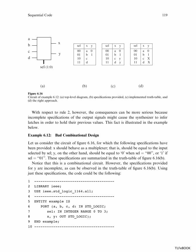
With respect to rule 2, however, the consequences can be more serious because
incomplete specifications of the output signals might cause the synthesizer to infer
latches in order to hold their previous values. This fact is illustrated in the example
below.
Example 6.12: Bad Combinational Design
Let us consider the circuit of figure 6.16, for which the following specifications have
been provided: x should behave as a multiplexer; that is, should be equal to the input
selected by sel; y, on the other hand, should be equal to ‘0’ when sel ¼ ‘‘00’’, or ‘1’ if
sel ¼ ‘‘01’’. These specifications are summarized in the truth-table of figure 6.16(b).
Notice that this is a combinational circuit. However, the specifications provided
for y are incomplete, as can be observed in the truth-table of figure 6.16(b). Using
just these specifications, the code could be the following:
1 --------------------------------------
2 LIBRARY ieee;
3 USE ieee.std_logic_1164.all;
4 --------------------------------------
5 ENTITY example IS
6 PORT (a, b, c, d: IN STD_LOGIC;
7 sel: IN INTEGER RANGE 0 TO 3;
8 x, y: OUT STD_LOGIC);
9 END example;
10 --------------------------------------
(a) (b) (c) (d)
sel x y
00011011
a 0 b 1 cd
sel (1:0)
a
b
c
dy
xsel x y
00011011
a 0 b 1 c yd y
sel x y
00011011
a 0 b 1 c Xd X
Figure 6.16Circuit of example 6.12: (a) top-level diagram, (b) specifications provided, (c) implemented truth-table, and(d) the right approach.
Sequential Code 119
TLFeBOOK

11 ARCHITECTURE example OF example IS
12 BEGIN
13 PROCESS (a, b, c, d, sel)
14 BEGIN
15 IF (sel=0) THEN
16 x<=a;
17 y<='0';
18 ELSIF (sel=1) THEN
19 x<=b;
20 y<='1';
21 ELSIF (sel=2) THEN
22 x<=c;
23 ELSE
24 x<=d;
25 END IF;
26 END PROCESS;
27 END example;
28 --------------------------------------
After compiling this code, the report files show that no flip-flops were inferred (as
expected). However, when we look at the simulation results (figure 6.17), we notice
something peculiar about y. Observe that, for the same value of the input
(sel ¼ 3 ¼ ‘‘11’’), two di¤erent results are obtained for y (when sel ¼ 3 is preceded by
sel ¼ 0, y ¼ ‘0’ results, while y ¼ ‘1’ is obtained when sel ¼ 3 is preceded by sel ¼ 1).
This signifies that some sort of memory was indeed implemented by the compiler. In
fact, if we look at the equations obtained with Quartus II, for example (appendix D),
we verify that y was computed as y ¼ (sel(0) AND sel(1)) OR (sel(0) AND y) OR
Figure 6.17Simulation results of example 6.12.
120 Chapter 6
TLFeBOOK
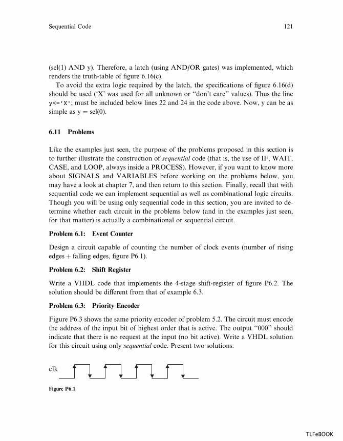
(sel(1) AND y). Therefore, a latch (using AND/OR gates) was implemented, which
renders the truth-table of figure 6.16(c).
To avoid the extra logic required by the latch, the specifications of figure 6.16(d)
should be used (‘X’ was used for all unknown or ‘‘don’t care’’ values). Thus the line
y<='X'; must be included below lines 22 and 24 in the code above. Now, y can be as
simple as y ¼ sel(0).
6.11 Problems
Like the examples just seen, the purpose of the problems proposed in this section is
to further illustrate the construction of sequential code (that is, the use of IF, WAIT,
CASE, and LOOP, always inside a PROCESS). However, if you want to know more
about SIGNALS and VARIABLES before working on the problems below, you
may have a look at chapter 7, and then return to this section. Finally, recall that with
sequential code we can implement sequential as well as combinational logic circuits.
Though you will be using only sequential code in this section, you are invited to de-
termine whether each circuit in the problems below (and in the examples just seen,
for that matter) is actually a combinational or sequential circuit.
Problem 6.1: Event Counter
Design a circuit capable of counting the number of clock events (number of rising
edgesþ falling edges, figure P6.1).
Problem 6.2: Shift Register
Write a VHDL code that implements the 4-stage shift-register of figure P6.2. The
solution should be di¤erent from that of example 6.3.
Problem 6.3: Priority Encoder
Figure P6.3 shows the same priority encoder of problem 5.2. The circuit must encode
the address of the input bit of highest order that is active. The output ‘‘000’’ should
indicate that there is no request at the input (no bit active). Write a VHDL solution
for this circuit using only sequential code. Present two solutions:
clk
Figure P6.1
Sequential Code 121
TLFeBOOK

(a) With IF.
(b) With CASE.
Problem 6.4: Generic Frequency Divider
Write a VHDL code for a circuit capable of dividing the frequency of an input clock
signal by an integer n (figure P6.4). The code should be generic; that is, n should be
defined using the GENERIC statement.
Problem 6.5: Frequency Multiplier
What about the opposite of problem 6.4, that is, say that we want to multiply the
clock frequency by n. Can it be done?
din
clk
dout
DFF DFF DFF DFF
Figure P6.2
‘0’‘1’‘0’‘0’‘1’’1’‘0’
7654321
210
PRIORITYENCODER
‘1’’1’‘0’
Figure P6.3
fclk fclk/nFREQ.
DIVIDER
Figure P6.4
122 Chapter 6
TLFeBOOK
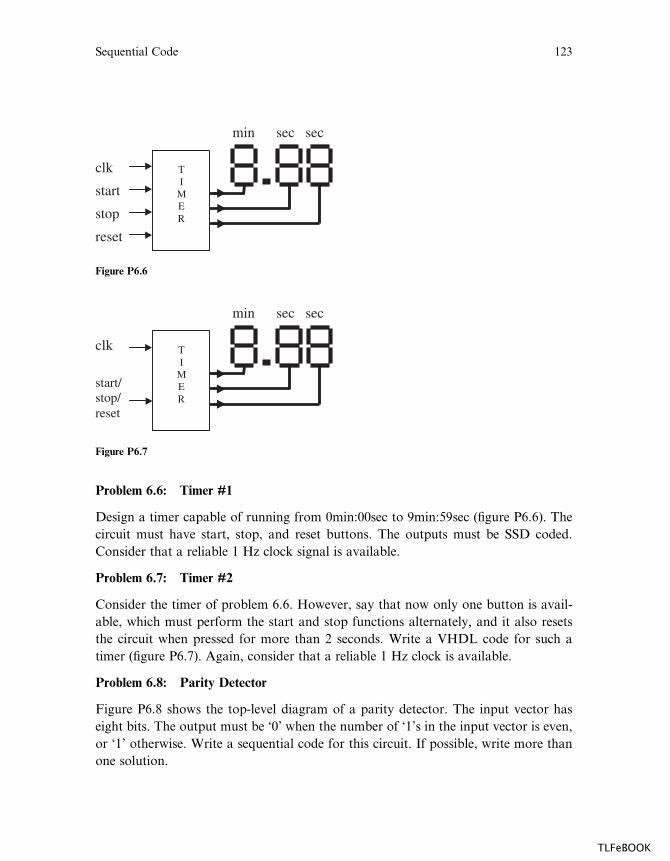
Problem 6.6: Timer #1
Design a timer capable of running from 0min:00sec to 9min:59sec (figure P6.6). The
circuit must have start, stop, and reset buttons. The outputs must be SSD coded.
Consider that a reliable 1 Hz clock signal is available.
Problem 6.7: Timer #2
Consider the timer of problem 6.6. However, say that now only one button is avail-
able, which must perform the start and stop functions alternately, and it also resets
the circuit when pressed for more than 2 seconds. Write a VHDL code for such a
timer (figure P6.7). Again, consider that a reliable 1 Hz clock is available.
Problem 6.8: Parity Detector
Figure P6.8 shows the top-level diagram of a parity detector. The input vector has
eight bits. The output must be ‘0’ when the number of ‘1’s in the input vector is even,
or ‘1’ otherwise. Write a sequential code for this circuit. If possible, write more than
one solution.
min sec sec
clk
start
stop
reset
TI
MER
Figure P6.6
clk
start/stop/reset
min sec sec
TI
MER
Figure P6.7
Sequential Code 123
TLFeBOOK
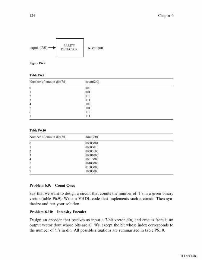
Problem 6.9: Count Ones
Say that we want to design a circuit that counts the number of ‘1’s in a given binary
vector (table P6.9). Write a VHDL code that implements such a circuit. Then syn-
thesize and test your solution.
Problem 6.10: Intensity Encoder
Design an encoder that receives as input a 7-bit vector din, and creates from it an
output vector dout whose bits are all ‘0’s, except the bit whose index corresponds to
the number of ‘1’s in din. All possible situations are summarized in table P6.10.
input (7:0) outputPARITY
DETECTOR
Figure P6.8
Table P6.9
Number of ones in din(7:1) count(2:0)
0 000
1 001
2 010
3 011
4 100
5 101
6 110
7 111
Table P6.10
Number of ones in din(7:1) dout(7:0)
0 00000001
1 00000010
2 00000100
3 00001000
4 00010000
5 00100000
6 01000000
7 10000000
124 Chapter 6
TLFeBOOK
Problem 6.11: Multiplexer
Write a sequential VHDL code for the circuit of problem 5.1. If possible, present
more than one solution.
Problem 6.12: Vector Shifter
Write a sequential VHDL code for the circuit of example 5.6. If possible, present
more than one solution.
Problem 6.13: ALU
Write a sequential VHDL code for the circuit of example 5.5. If possible, present
more than one solution.
Problem 6.14: Signed/Unsigned Adder/Subtractor
Solve problem 5.5 using sequential code. Make the code as generic as possible.
Problem 6.15: Comparator
Solve problem 5.8 using sequential code.
Problem 6.16: Carry Ripple Adder
Consider the carry ripple adder of example 6.8.
(a) Why cannot we replace the IF statement of lines 17–19 in solution 2 by simply
‘‘temp:=c0;’’?
(b) Notice that the circuit of example 6.8 is fully combinational, so it can also be
implemented using only concurrent code (that is, without a PROCESS). Write such a
code for it. Then simulate it and analyze the results.
Problem 6.17: DFF
Consider the DFF with asynchronous reset of figure 6.1. Below are several codes for
that circuit. Examine each of them and determine whether they should work prop-
erly. Briefly explain your answers.
--------------------------------------
LIBRARY ieee;
USE ieee.std_logic_1164.all;
--------------------------------------
ENTITY dff IS
Sequential Code 125
TLFeBOOK
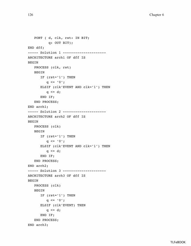
PORT ( d, clk, rst: IN BIT;
q: OUT BIT);
END dff;
----- Solution 1 ---------------------
ARCHITECTURE arch1 OF dff IS
BEGIN
PROCESS (clk, rst)
BEGIN
IF (rst='1') THEN
q <= '0';
ELSIF (clk'EVENT AND clk='1') THEN
q <= d;
END IF;
END PROCESS;
END arch1;
----- Solution 2 ---------------------
ARCHITECTURE arch2 OF dff IS
BEGIN
PROCESS (clk)
BEGIN
IF (rst='1') THEN
q <= '0';
ELSIF (clk'EVENT AND clk='1') THEN
q <= d;
END IF;
END PROCESS;
END arch2;
----- Solution 3 ---------------------
ARCHITECTURE arch3 OF dff IS
BEGIN
PROCESS (clk)
BEGIN
IF (rst='1') THEN
q <= '0';
ELSIF (clk'EVENT) THEN
q <= d;
END IF;
END PROCESS;
END arch3;
126 Chapter 6
TLFeBOOK
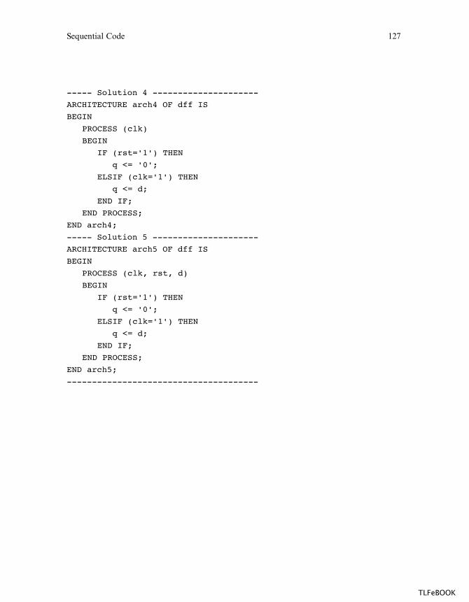
----- Solution 4 ---------------------
ARCHITECTURE arch4 OF dff IS
BEGIN
PROCESS (clk)
BEGIN
IF (rst='1') THEN
q <= '0';
ELSIF (clk='1') THEN
q <= d;
END IF;
END PROCESS;
END arch4;
----- Solution 5 ---------------------
ARCHITECTURE arch5 OF dff IS
BEGIN
PROCESS (clk, rst, d)
BEGIN
IF (rst='1') THEN
q <= '0';
ELSIF (clk='1') THEN
q <= d;
END IF;
END PROCESS;
END arch5;
--------------------------------------
Sequential Code 127
TLFeBOOK

TLFeBOOK
7 Signals and Variables
VHDL provides two objects for dealing with non-static data values: SIGNAL and
VARIABLE. It also provides means for establishing default (static) values: CON-
STANT and GENERIC. The last of these (the GENERIC attribute) was already
seen in chapter 4. SIGNAL, VARIABLE, and CONSTANT will be studied together
in this chapter.
CONSTANT and SIGNAL can be global (that is, seen by the whole code), and
can be used in either type of code, concurrent or sequential. A VARIABLE, on the
other hand, is local, for it can only be used inside a piece of sequential code (that is,
in a PROCESS, FUNCTION, or PROCEDURE) and its value can never be passed
out directly.
As will become apparent, the choice between a SIGNAL or a VARIABLE is not
always easy, so an entire section and several examples will be devoted to the matter.
Moreover, a discussion on the number of registers inferred by the compiler, based on
SIGNAL and VARIABLE assignments, will also be presented.
7.1 CONSTANT
CONSTANT serves to establish default values. Its syntax is shown below.
CONSTANT name : type := value;
Examples:
CONSTANT set_bit : BIT := '1';
CONSTANT datamemory : memory := (('0','0','0','0'),
('0','0','0','1'),
('0','0','1','1'));
A CONSTANT can be declared in a PACKAGE, ENTITY, or ARCHITEC-
TURE. When declared in a package, it is truly global, for the package can be
used by several entities. When declared in an entity (after PORT), it is global to all
architectures that follow that entity. Finally, when declared in an architecture (in its
declarative part), it is global only to that architecture’s code. The most common
places to find a CONSTANT declaration is in an ARCHITECTURE or in a
PACKAGE.
TLFeBOOK
7.2 SIGNAL
SIGNAL serves to pass values in and out the circuit, as well as between its internal
units. In other words, a signal represents circuit interconnects (wires). For instance,
all PORTS of an ENTITY are signals by default. Its syntax is the following:
SIGNAL name : type [range] [:= initial_value];
Examples:
SIGNAL control: BIT := '0';
SIGNAL count: INTEGER RANGE 0 TO 100;
SIGNAL y: STD_LOGIC_VECTOR (7 DOWNTO 0);
The declaration of a SIGNAL can be made in the same places as the declaration
of a CONSTANT (described above).
A very important aspect of a SIGNAL, when used inside a section of sequential
code (PROCESS, for example), is that its update is not immediate. In other words, its
new value should not be expected to be ready before the conclusion of the corre-
sponding PROCESS, FUNCTION or PROCEDURE.
Recall that the assignment operator for a SIGNAL is ‘‘<=’’ (Ex.: count<=35;).
Also, the initial value in the syntax above is not synthesizable, being only considered
in simulations.
Another aspect that might a¤ect the result is when multiple assignments are made
to the same SIGNAL. The compiler might complain and quit synthesis, or might
infer the wrong circuit (by considering only the last assignment, for example).
Therefore, establishing initial values, like in line 15 of the example below, should be
done with a VARIABLE.
Example 7.1: Count Ones #1 (not OK)
Say that we want to design a circuit that counts the number of ‘1’s in a binary vector
(problem 6.9). Let us consider the solution below, which uses only signals. This code
has multiple assignments to the same signal, temp, in lines 15 (once) and 18 (eight
times). Moreover, since the value of a signal is not updated immediately, line 18
conflicts with line 15, for the value assigned in line 15 might not be ready until the
conclusion of the PROCESS, in which case a wrong value would be computed in line
18. In this kind of situation, the use of a VARIABLE is recommended (example 7.2).
130 Chapter 7
TLFeBOOK
1 ---------------------------------------
2 LIBRARY ieee;
3 USE ieee.std_logic_1164.all;
4 ---------------------------------------
5 ENTITY count_ones IS
6 PORT ( din: IN STD_LOGIC_VECTOR (7 DOWNTO 0);
7 ones: OUT INTEGER RANGE 0 TO 8);
8 END count_ones;
9 ---------------------------------------
10 ARCHITECTURE not_ok OF count_ones IS
11 SIGNAL temp: INTEGER RANGE 0 TO 8;
12 BEGIN
13 PROCESS (din)
14 BEGIN
15 temp <= 0;
16 FOR i IN 0 TO 7 LOOP
17 IF (din(i)='1') THEN
18 temp <= temp + 1;
19 END IF;
20 END LOOP;
21 ones <= temp;
22 END PROCESS;
23 END not_ok;
24 ---------------------------------------
Notice also in the solution above that the internal signal temp (line 11) seems un-
necessary, because ones could have been used directly. However, to do so, the mode
of ones would need to be changed from OUT to BUFFER (line 7), because ones is
assigned a value and is also read (used) internally. Nevertheless, since ones is a gen-
uine unidirectional (OUT) signal, the use of an auxiliary signal (temp) is an adequate
design practice.
7.3 VARIABLE
Contrary to CONSTANT and SIGNAL, a VARIABLE represents only local infor-
mation. It can only be used inside a PROCESS, FUNCTION, or PROCEDURE
(that is, in sequential code), and its value can not be passed out directly. On the other
hand, its update is immediate, so the new value can be promptly used in the next line
of code.
Signals and Variables 131
TLFeBOOK

To declare a VARIABLE, the following syntax should be used:
VARIABLE name : type [range] [:= init_value];
Examples:
VARIABLE control: BIT := '0';
VARIABLE count: INTEGER RANGE 0 TO 100;
VARIABLE y: STD_LOGIC_VECTOR (7 DOWNTO 0) := "10001000";
Since a VARIABLE can only be used in sequential code, its declaration can only
be done in the declarative part of a PROCESS, FUNCTION, or PROCEDURE.
Recall that the assignment operator for a VARIABLE is ‘‘:=’’ (Ex.: count:=35;).
Also, like in the case of a SIGNAL, the initial value in the syntax above is not syn-
thesizable, being only considered in simulations.
Example 7.2: Count Ones #2 (OK)
Let us consider the problem of example 7.1 once again. The only di¤erence in the
solution below is that an internal VARIABLE is employed instead of a SIGNAL.
Since the update of a variable is immediate, the initial value is established correctly
and no complains regarding multiple assignments will be issued by the compiler.
Simulation results can be verified in figure 7.1.
1 ---------------------------------------
2 LIBRARY ieee;
3 USE ieee.std_logic_1164.all;
4 ---------------------------------------
5 ENTITY count_ones IS
6 PORT ( din: IN STD_LOGIC_VECTOR (7 DOWNTO 0);
7 ones: OUT INTEGER RANGE 0 TO 8);
Figure 7.1Simulation results of example 7.2.
132 Chapter 7
TLFeBOOK
8 END count_ones;
9 ---------------------------------------
10 ARCHITECTURE ok OF count_ones IS
11 BEGIN
12 PROCESS (din)
13 VARIABLE temp: INTEGER RANGE 0 TO 8;
14 BEGIN
15 temp := 0;
16 FOR i IN 0 TO 7 LOOP
17 IF (din(i)='1') THEN
18 temp := temp + 1;
19 END IF;
20 END LOOP;
21 ones <= temp;
22 END PROCESS;
23 END ok;
24 ---------------------------------------
7.4 SIGNAL versus VARIABLE
As already mentioned, choosing between a SIGNAL or a VARIABLE is not always
straightforward. Their main di¤erences are summarized in table 7.1.
Table 7.1Comparison between SIGNAL and VARIABLE.
SIGNAL VARIABLE
Assignment <¼ :¼Utility Represents circuit interconnects (wires) Represents local information
Scope Can be global (seen by entire code) Local (visible only inside thecorresponding PROCESS, FUNCTION,or PROCEDURE)
Behavior Update is not immediate in sequentialcode (new value generally only availableat the conclusion of the PROCESS,FUNCTION, or PROCEDURE)
Updated immediately (new value can beused in the next line of code)
Usage In a PACKAGE, ENTITY, orARCHITECTURE. In an ENTITY, allPORTS are SIGNALS by default
Only in sequential code, that is, in aPROCESS, FUNCTION, orPROCEDURE
Signals and Variables 133
TLFeBOOK

We want to stress again that an assignment to a VARIABLE is immediate, but
that is not the case with a SIGNAL. In general, the new value of a SIGNAL will
only be available at the conclusion of the current run of the corresponding PRO-
CESS. Though this might not be always the case, it is a safe practice to consider it so.
The examples presented below will further illustrate this and other di¤erences be-
tween SIGNALS and VARIABLES.
Example 7.3: Bad versus Good Multiplexer
In this example, we will implement the same multiplexer of example 5.2 (repeated in
figure 7.2). This is, indeed, a classical example regarding the choice of a SIGNAL
versus a VARIABLE.
1 -- Solution 1: using a SIGNAL (not ok) --
2 LIBRARY ieee;
3 USE ieee.std_logic_1164.all;
4 -----------------------------------------
5 ENTITY mux IS
6 PORT ( a, b, c, d, s0, s1: IN STD_LOGIC;
7 y: OUT STD_LOGIC);
8 END mux;
9 -----------------------------------------
10 ARCHITECTURE not_ok OF mux IS
11 SIGNAL sel : INTEGER RANGE 0 TO 3;
12 BEGIN
13 PROCESS (a, b, c, d, s0, s1)
14 BEGIN
15 sel <= 0;
16 IF (s0='1') THEN sel <= sel + 1;
sel (1:0)
a
b
c
d
yMUX
Figure 7.2Multiplexer of example 7.3.
134 Chapter 7
TLFeBOOK

17 END IF;
18 IF (s1='1') THEN sel <= sel + 2;
19 END IF;
20 CASE sel IS
21 WHEN 0 => y<=a;
22 WHEN 1 => y<=b;
23 WHEN 2 => y<=c;
24 WHEN 3 => y<=d;
25 END CASE;
26 END PROCESS;
27 END not_ok;
28 -----------------------------------------
1 -- Solution 2: using a VARIABLE (ok) ----
2 LIBRARY ieee;
3 USE ieee.std_logic_1164.all;
4 -----------------------------------------
5 ENTITY mux IS
6 PORT ( a, b, c, d, s0, s1: IN STD_LOGIC;
7 y: OUT STD_LOGIC);
8 END mux;
9 -----------------------------------------
10 ARCHITECTURE ok OF mux IS
11 BEGIN
12 PROCESS (a, b, c, d, s0, s1)
13 VARIABLE sel : INTEGER RANGE 0 TO 3;
14 BEGIN
15 sel := 0;
16 IF (s0='1') THEN sel := sel + 1;
17 END IF;
18 IF (s1='1') THEN sel := sel + 2;
19 END IF;
20 CASE sel IS
21 WHEN 0 => y<=a;
22 WHEN 1 => y<=b;
23 WHEN 2 => y<=c;
24 WHEN 3 => y<=d;
25 END CASE;
Signals and Variables 135
TLFeBOOK
26 END PROCESS;
27 END ok;
28 ---------------------------------------
Comments:
A common mistake when using a SIGNAL is not to remember that it might require
a certain amount of time to be updated. Therefore, the assignment sel <¼ selþ 1 in
the first solution (line 16) will result in one plus whatever value had been previously
propagated to sel, for the assignment sel <¼ 0 (line 15) might not have had time to
propagate yet. The same is true for sel <¼ selþ 2 (line 18). This is not a problem
when using a VARIABLE, for its assignment is always immediate.
A second aspect that might be a problem in solution 1 is that more than one as-
signment is being made to the same SIGNAL (sel, lines 15, 16, and 18), which might
not be acceptable. Generally, only one assignment to a SIGNAL is allowed within a
PROCESS, so the software will either consider only the last one (sel <¼ selþ 2 in
solution 1) or simply issue an error message and stop compilation. Again, this is
never a problem when using a VARIABLE.
Figure 7.3Simulation results of example 7.3.
136 Chapter 7
TLFeBOOK
Simulation results from both solutions are shown in figure 7.3 (bad mux in the
upper graph, good mux in the lower graph). As can be seen, only solution 2 works
properly.
Example 7.4: DFF with q and qbar #1
We want to implement the DFF of figure 7.4. This circuit di¤ers from that of exam-
ple 6.1 by the absence of reset and the inclusion of qbar. The presence of qbar will
help understand how an assignment to a SIGNAL is made (recall that a PORT is a
SIGNAL by default).
1 ---- Solution 1: not OK ---------------
2 LIBRARY ieee;
3 USE ieee.std_logic_1164.all;
4 ---------------------------------------
5 ENTITY dff IS
6 PORT ( d, clk: IN STD_LOGIC;
7 q: BUFFER STD_LOGIC;
8 qbar: OUT STD_LOGIC);
9 END dff;
10 ---------------------------------------
11 ARCHITECTURE not_ok OF dff IS
12 BEGIN
13 PROCESS (clk)
14 BEGIN
15 IF (clk'EVENT AND clk='1') THEN
16 q <= d;
17 qbar <= NOT q;
18 END IF;
19 END PROCESS;
20 END not_ok;
21 ---------------------------------------
d
clk
q
qbar
DFF
Figure 7.4DFF of example 7.4.
Signals and Variables 137
TLFeBOOK
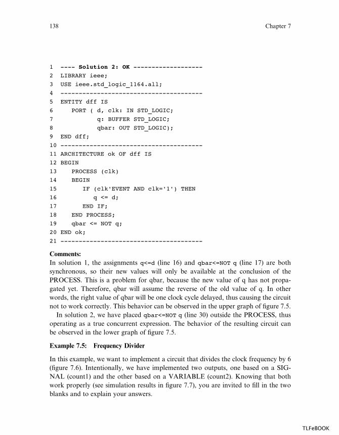
1 ---- Solution 2: OK -------------------
2 LIBRARY ieee;
3 USE ieee.std_logic_1164.all;
4 ---------------------------------------
5 ENTITY dff IS
6 PORT ( d, clk: IN STD_LOGIC;
7 q: BUFFER STD_LOGIC;
8 qbar: OUT STD_LOGIC);
9 END dff;
10 ---------------------------------------
11 ARCHITECTURE ok OF dff IS
12 BEGIN
13 PROCESS (clk)
14 BEGIN
15 IF (clk'EVENT AND clk='1') THEN
16 q <= d;
17 END IF;
18 END PROCESS;
19 qbar <= NOT q;
20 END ok;
21 ---------------------------------------
Comments:
In solution 1, the assignments q<=d (line 16) and qbar<=NOT q (line 17) are both
synchronous, so their new values will only be available at the conclusion of the
PROCESS. This is a problem for qbar, because the new value of q has not propa-
gated yet. Therefore, qbar will assume the reverse of the old value of q. In other
words, the right value of qbar will be one clock cycle delayed, thus causing the circuit
not to work correctly. This behavior can be observed in the upper graph of figure 7.5.
In solution 2, we have placed qbar<=NOT q (line 30) outside the PROCESS, thus
operating as a true concurrent expression. The behavior of the resulting circuit can
be observed in the lower graph of figure 7.5.
Example 7.5: Frequency Divider
In this example, we want to implement a circuit that divides the clock frequency by 6
(figure 7.6). Intentionally, we have implemented two outputs, one based on a SIG-
NAL (count1) and the other based on a VARIABLE (count2). Knowing that both
work properly (see simulation results in figure 7.7), you are invited to fill in the two
blanks and to explain your answers.
138 Chapter 7
TLFeBOOK
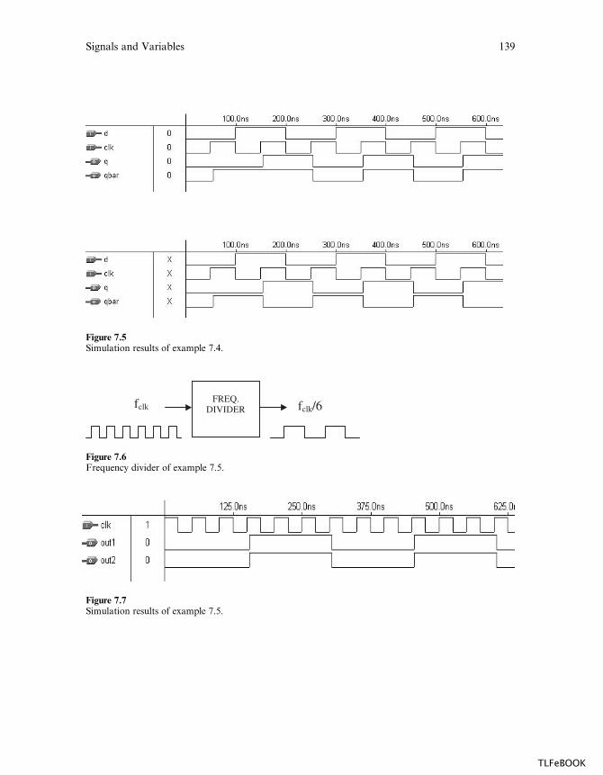
Figure 7.5Simulation results of example 7.4.
fclk fclk/6FREQ.
DIVIDER
Figure 7.6Frequency divider of example 7.5.
Figure 7.7Simulation results of example 7.5.
Signals and Variables 139
TLFeBOOK

1 -----------------------------------------
2 LIBRARY ieee;
3 USE ieee.std_logic_1164.all;
4 -----------------------------------------
5 ENTITY freq_divider IS
6 PORT ( clk : IN STD_LOGIC;
7 out1, out2 : BUFFER STD_LOGIC);
8 END freq_divider;
9 -----------------------------------------
10 ARCHITECTURE example OF freq_divider IS
11 SIGNAL count1 : INTEGER RANGE 0 TO 7;
12 BEGIN
13 PROCESS (clk)
14 VARIABLE count2 : INTEGER RANGE 0 TO 7;
15 BEGIN
16 IF (clk'EVENT AND clk='1') THEN
17 count1 <= count1 + 1;
18 count2 := count2 + 1;
19 IF (count1 = ? ) THEN
20 out1 <= NOT out1;
21 count1 <= 0;
22 END IF;
23 IF (count2 = ? ) THEN
24 out2 <= NOT out2;
25 count2 := 0;
26 END IF;
27 END IF;
28 END PROCESS;
29 END example;
30 -----------------------------------------
7.5 Number of Registers
In this section, we will discuss the number of flip-flops inferred from the code
by the compiler. The purpose is not only to understand which approaches require
less registers, but also to make sure that the code does implement the expected
circuit.
140 Chapter 7
TLFeBOOK

A SIGNAL generates a flip-flop whenever an assignment is made at the transition
of another signal; that is, when a synchronous assignment occurs. Such assignment,
being synchronous, can only happen inside a PROCESS, FUNCTION, or PRO-
CEDURE (usually following a declaration of the type ‘‘IF signal’EVENT . . .’’ or
‘‘WAIT UNTIL . . .’’).
A VARIABLE, on the other hand, will not necessarily generate flip-flops if its
value never leaves the PROCESS (or FUNCTION, or PROCEDURE). However, if
a value is assigned to a variable at the transition of another signal, and such value is
eventually passed to a signal (which leaves the process), then flip-flops will be in-
ferred. A VARIABLE also generates a register when it is used before a value has
been assigned to it. The examples presented below will illustrate these points.
Example: In the process shown below, output1 and output2 will both be stored (that
is, infer flip-flops), because both are assigned at the transition of another signal (clk).
PROCESS (clk)
BEGIN
IF (clk'EVENT AND clk='1') THEN
output1 <= temp; -- output1 stored
output2 <= a; -- output2 stored
END IF;
END PROCESS;
Example: In the next process, only output1 will be stored (output2 will make use of
logic gates).
PROCESS (clk)
BEGIN
IF (clk'EVENT AND clk='1') THEN
output1 <= temp; -- output1 stored
END IF;
output2 <= a; -- output2 not stored
END PROCESS;
Example: In the process below, temp (a variable) will cause x (a signal) to be stored.
PROCESS (clk)
VARIABLE temp: BIT;
BEGIN
IF (clk'EVENT AND clk='1') THEN
Signals and Variables 141
TLFeBOOK
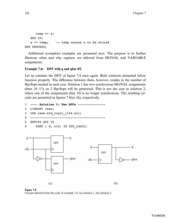
temp <= a;
END IF;
x <= temp; -- temp causes x to be stored
END PROCESS;
Additional (complete) examples are presented next. The purpose is to further
illustrate when and why registers are inferred from SIGNAL and VARIABLE
assignments.
Example 7.6: DFF with q and qbar #2
Let us consider the DFF of figure 7.4 once again. Both solutions presented below
function properly. The di¤erence between them, however, resides in the number of
flip-flops needed in each case. Solution 1 has two synchronous SIGNAL assignments
(lines 16–17), so 2 flip-flops will be generated. This is not the case in solution 2,
where one of the assignments (line 19) is no longer synchronous. The resulting cir-
cuits are presented in figures 7.8(a)–(b), respectively.
1 ---- Solution 1: Two DFFs ---------------
2 LIBRARY ieee;
3 USE ieee.std_logic_1164.all;
4 -----------------------------------------
5 ENTITY dff IS
6 PORT ( d, clk: IN STD_LOGIC;
d
clk
q
(a) (b)
DFF
qbar
DFF
d
clk
q
qbar
DFF
Figure 7.8Circuits inferred from the code of example 7.6: (a) solution 1, (b) solution 2.
142 Chapter 7
TLFeBOOK

7 q: BUFFER STD_LOGIC;
8 qbar: OUT STD_LOGIC);
9 END dff;
10 -----------------------------------------
11 ARCHITECTURE two_dff OF dff IS
12 BEGIN
13 PROCESS (clk)
14 BEGIN
15 IF (clk'EVENT AND clk='1') THEN
16 q <= d; -- generates a register
17 qbar <= NOT d; -- generates a register
18 END IF;
19 END PROCESS;
20 END two_dff;
21 -----------------------------------------
1 ---- Solution 2: One DFF ----------------
2 LIBRARY ieee;
3 USE ieee.std_logic_1164.all;
4 -----------------------------------------
5 ENTITY dff IS
6 PORT ( d, clk: IN STD_LOGIC;
7 q: BUFFER STD_LOGIC;
8 qbar: OUT STD_LOGIC);
9 END dff;
10 -----------------------------------------
11 ARCHITECTURE one_dff OF dff IS
12 BEGIN
13 PROCESS (clk)
14 BEGIN
15 IF (clk'EVENT AND clk='1') THEN
16 q <= d; -- generates a register
17 END IF;
18 END PROCESS;
19 qbar <= NOT q; -- uses logic gate (no register)
20 END one_dff;
21 -----------------------------------------
Signals and Variables 143
TLFeBOOK
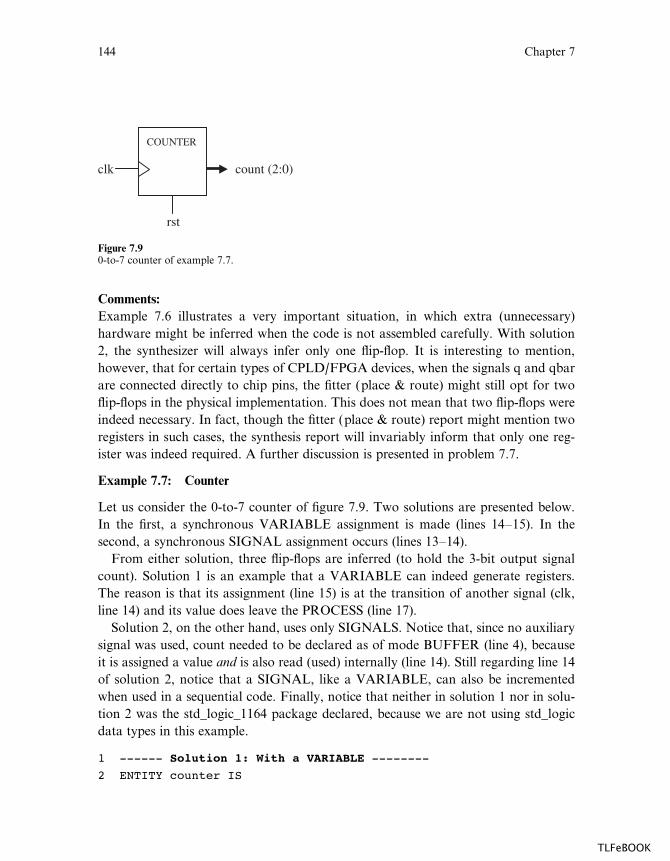
Comments:
Example 7.6 illustrates a very important situation, in which extra (unnecessary)
hardware might be inferred when the code is not assembled carefully. With solution
2, the synthesizer will always infer only one flip-flop. It is interesting to mention,
however, that for certain types of CPLD/FPGA devices, when the signals q and qbar
are connected directly to chip pins, the fitter (place & route) might still opt for two
flip-flops in the physical implementation. This does not mean that two flip-flops were
indeed necessary. In fact, though the fitter (place & route) report might mention two
registers in such cases, the synthesis report will invariably inform that only one reg-
ister was indeed required. A further discussion is presented in problem 7.7.
Example 7.7: Counter
Let us consider the 0-to-7 counter of figure 7.9. Two solutions are presented below.
In the first, a synchronous VARIABLE assignment is made (lines 14–15). In the
second, a synchronous SIGNAL assignment occurs (lines 13–14).
From either solution, three flip-flops are inferred (to hold the 3-bit output signal
count). Solution 1 is an example that a VARIABLE can indeed generate registers.
The reason is that its assignment (line 15) is at the transition of another signal (clk,
line 14) and its value does leave the PROCESS (line 17).
Solution 2, on the other hand, uses only SIGNALS. Notice that, since no auxiliary
signal was used, count needed to be declared as of mode BUFFER (line 4), because
it is assigned a value and is also read (used) internally (line 14). Still regarding line 14
of solution 2, notice that a SIGNAL, like a VARIABLE, can also be incremented
when used in a sequential code. Finally, notice that neither in solution 1 nor in solu-
tion 2 was the std_logic_1164 package declared, because we are not using std_logic
data types in this example.
1 ------ Solution 1: With a VARIABLE --------
2 ENTITY counter IS
clk count (2:0)
COUNTER
rst
Figure 7.90-to-7 counter of example 7.7.
144 Chapter 7
TLFeBOOK
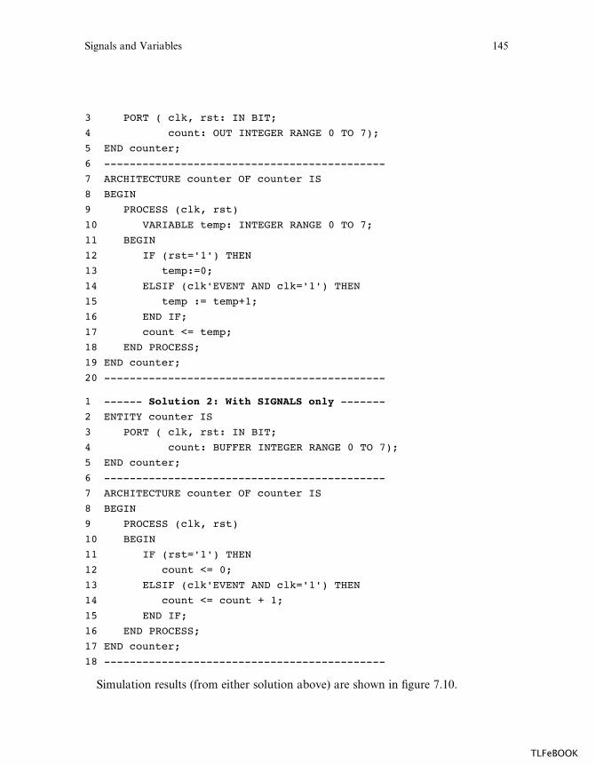
3 PORT ( clk, rst: IN BIT;
4 count: OUT INTEGER RANGE 0 TO 7);
5 END counter;
6 --------------------------------------------
7 ARCHITECTURE counter OF counter IS
8 BEGIN
9 PROCESS (clk, rst)
10 VARIABLE temp: INTEGER RANGE 0 TO 7;
11 BEGIN
12 IF (rst='1') THEN
13 temp:=0;
14 ELSIF (clk'EVENT AND clk='1') THEN
15 temp := temp+1;
16 END IF;
17 count <= temp;
18 END PROCESS;
19 END counter;
20 --------------------------------------------
1 ------ Solution 2: With SIGNALS only -------
2 ENTITY counter IS
3 PORT ( clk, rst: IN BIT;
4 count: BUFFER INTEGER RANGE 0 TO 7);
5 END counter;
6 --------------------------------------------
7 ARCHITECTURE counter OF counter IS
8 BEGIN
9 PROCESS (clk, rst)
10 BEGIN
11 IF (rst='1') THEN
12 count <= 0;
13 ELSIF (clk'EVENT AND clk='1') THEN
14 count <= count + 1;
15 END IF;
16 END PROCESS;
17 END counter;
18 --------------------------------------------
Simulation results (from either solution above) are shown in figure 7.10.
Signals and Variables 145
TLFeBOOK
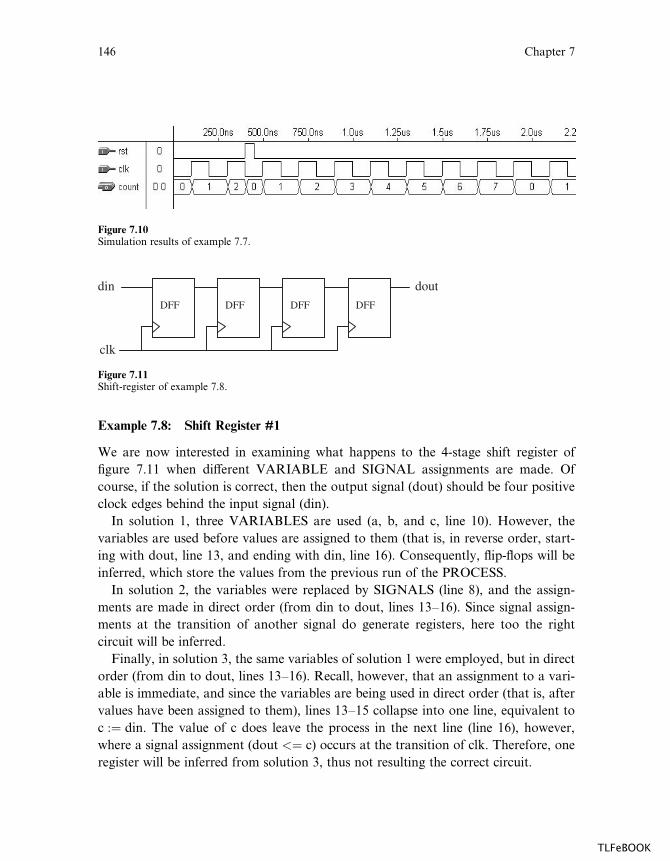
Example 7.8: Shift Register #1
We are now interested in examining what happens to the 4-stage shift register of
figure 7.11 when di¤erent VARIABLE and SIGNAL assignments are made. Of
course, if the solution is correct, then the output signal (dout) should be four positive
clock edges behind the input signal (din).
In solution 1, three VARIABLES are used (a, b, and c, line 10). However, the
variables are used before values are assigned to them (that is, in reverse order, start-
ing with dout, line 13, and ending with din, line 16). Consequently, flip-flops will be
inferred, which store the values from the previous run of the PROCESS.
In solution 2, the variables were replaced by SIGNALS (line 8), and the assign-
ments are made in direct order (from din to dout, lines 13–16). Since signal assign-
ments at the transition of another signal do generate registers, here too the right
circuit will be inferred.
Finally, in solution 3, the same variables of solution 1 were employed, but in direct
order (from din to dout, lines 13–16). Recall, however, that an assignment to a vari-
able is immediate, and since the variables are being used in direct order (that is, after
values have been assigned to them), lines 13–15 collapse into one line, equivalent to
c :¼ din. The value of c does leave the process in the next line (line 16), however,
where a signal assignment (dout <¼ c) occurs at the transition of clk. Therefore, one
register will be inferred from solution 3, thus not resulting the correct circuit.
Figure 7.10Simulation results of example 7.7.
din
clk
dout
DFF DFF DFF DFF
Figure 7.11Shift-register of example 7.8.
146 Chapter 7
TLFeBOOK
Note: More conventional solutions to the shift-register problem will be presented in
example 7.9.
1 -------- Solution 1: -----------------
2 ENTITY shift IS
3 PORT ( din, clk: IN BIT;
4 dout: OUT BIT);
5 END shift;
6 --------------------------------------
7 ARCHITECTURE shift OF shift IS
8 BEGIN
9 PROCESS (clk)
10 VARIABLE a, b, c: BIT;
11 BEGIN
12 IF (clk'EVENT AND clk='1') THEN
13 dout <= c;
14 c := b;
15 b := a;
16 a := din;
17 END IF;
18 END PROCESS;
19 END shift;
20 --------------------------------------
1 -------- Solution 2: -----------------
2 ENTITY shift IS
3 PORT ( din, clk: IN BIT;
4 dout: OUT BIT);
5 END shift;
6 --------------------------------------
7 ARCHITECTURE shift OF shift IS
8 SIGNAL a, b, c: BIT;
9 BEGIN
10 PROCESS (clk)
11 BEGIN
12 IF (clk'EVENT AND clk='1') THEN
13 a <= din;
14 b <= a;
Signals and Variables 147
TLFeBOOK
15 c <= b;
16 dout <= c;
17 END IF;
18 END PROCESS;
19 END shift;
20 --------------------------------------
1 -------- Solution 3: -----------------
2 ENTITY shift IS
3 PORT ( din, clk: IN BIT;
4 dout: OUT BIT);
5 END shift;
6 --------------------------------------
7 ARCHITECTURE shift OF shift IS
8 BEGIN
9 PROCESS (clk)
10 VARIABLE a, b, c: BIT;
11 BEGIN
12 IF (clk'EVENT AND clk='1') THEN
13 a := din;
14 b := a;
15 c := b;
16 dout <= c;
17 END IF;
18 END PROCESS;
19 END shift;
20 --------------------------------------
Simulation results from solution 1 or 2 are shown in the upper graph of figure
7.12, while the lower graph shows results from solution 3. As expected, dout is four
positive clock edges behind din in the former, but only one positive edge behind the
input in the latter.
Example 7.9: Shift Register #2
In this example, conventional approaches to the design of shift registers are presented.
Figure 7.13 shows a 4-bit shift register, similar to that of example 7.8, except for
the presence of a reset input (rst). As before, the output bit (q) should be four positive
clock edges behind the input bit (d). Reset should be asynchronous, forcing all flip-
flop outputs to ‘0’ when asserted.
148 Chapter 7
TLFeBOOK
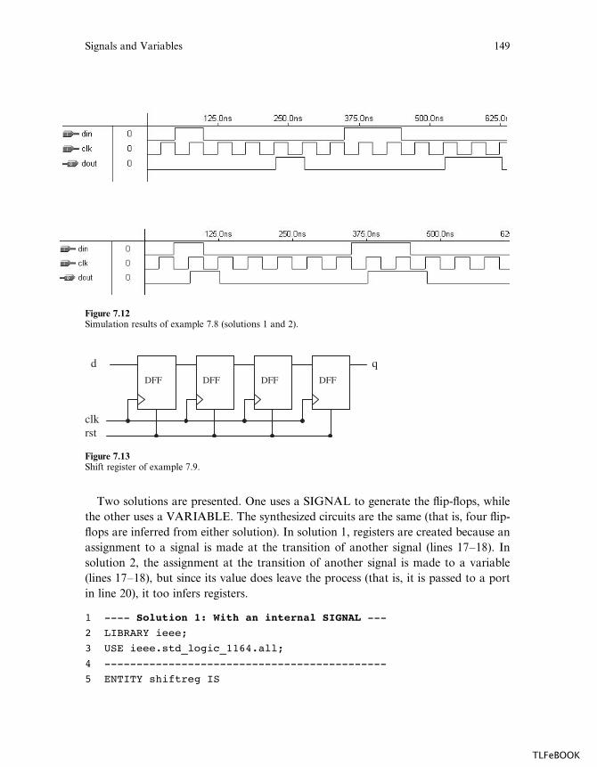
Two solutions are presented. One uses a SIGNAL to generate the flip-flops, while
the other uses a VARIABLE. The synthesized circuits are the same (that is, four flip-
flops are inferred from either solution). In solution 1, registers are created because an
assignment to a signal is made at the transition of another signal (lines 17–18). In
solution 2, the assignment at the transition of another signal is made to a variable
(lines 17–18), but since its value does leave the process (that is, it is passed to a port
in line 20), it too infers registers.
1 ---- Solution 1: With an internal SIGNAL ---
2 LIBRARY ieee;
3 USE ieee.std_logic_1164.all;
4 --------------------------------------------
5 ENTITY shiftreg IS
Figure 7.12Simulation results of example 7.8 (solutions 1 and 2).
d
clkrst
q
DFF DFF DFF DFF
Figure 7.13Shift register of example 7.9.
Signals and Variables 149
TLFeBOOK
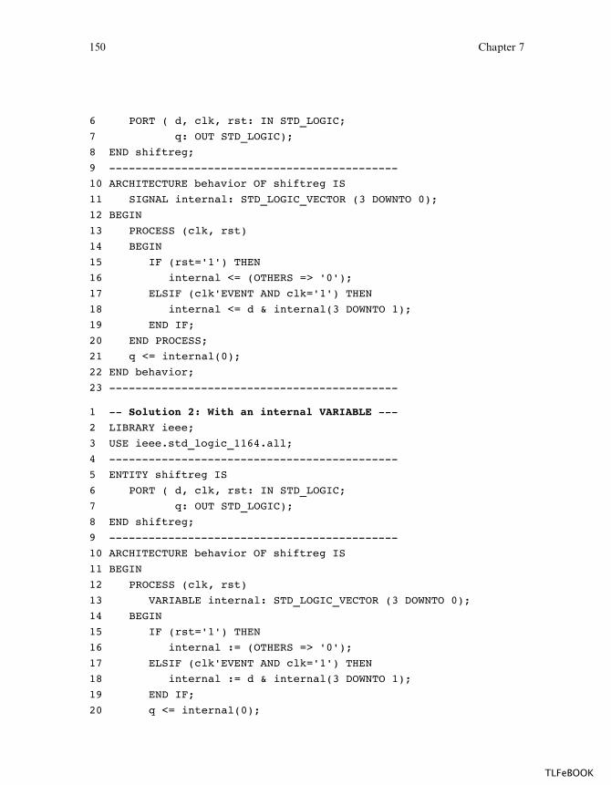
6 PORT ( d, clk, rst: IN STD_LOGIC;
7 q: OUT STD_LOGIC);
8 END shiftreg;
9 --------------------------------------------
10 ARCHITECTURE behavior OF shiftreg IS
11 SIGNAL internal: STD_LOGIC_VECTOR (3 DOWNTO 0);
12 BEGIN
13 PROCESS (clk, rst)
14 BEGIN
15 IF (rst='1') THEN
16 internal <= (OTHERS => '0');
17 ELSIF (clk'EVENT AND clk='1') THEN
18 internal <= d & internal(3 DOWNTO 1);
19 END IF;
20 END PROCESS;
21 q <= internal(0);
22 END behavior;
23 --------------------------------------------
1 -- Solution 2: With an internal VARIABLE ---
2 LIBRARY ieee;
3 USE ieee.std_logic_1164.all;
4 --------------------------------------------
5 ENTITY shiftreg IS
6 PORT ( d, clk, rst: IN STD_LOGIC;
7 q: OUT STD_LOGIC);
8 END shiftreg;
9 --------------------------------------------
10 ARCHITECTURE behavior OF shiftreg IS
11 BEGIN
12 PROCESS (clk, rst)
13 VARIABLE internal: STD_LOGIC_VECTOR (3 DOWNTO 0);
14 BEGIN
15 IF (rst='1') THEN
16 internal := (OTHERS => '0');
17 ELSIF (clk'EVENT AND clk='1') THEN
18 internal := d & internal(3 DOWNTO 1);
19 END IF;
20 q <= internal(0);
150 Chapter 7
TLFeBOOK
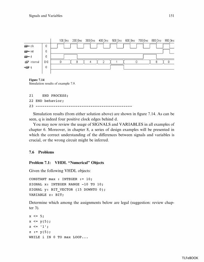
21 END PROCESS;
22 END behavior;
23 --------------------------------------------
Simulation results (from either solution above) are shown in figure 7.14. As can be
seen, q is indeed four positive clock edges behind d.
You may now review the usage of SIGNALS and VARIABLES in all examples of
chapter 6. Moreover, in chapter 8, a series of design examples will be presented in
which the correct understanding of the di¤erences between signals and variables is
crucial, or the wrong circuit might be inferred.
7.6 Problems
Problem 7.1: VHDL ‘‘Numerical’’ Objects
Given the following VHDL objects:
CONSTANT max : INTEGER := 10;
SIGNAL x: INTEGER RANGE -10 TO 10;
SIGNAL y: BIT_VECTOR (15 DOWNTO 0);
VARIABLE z: BIT;
Determine which among the assignments below are legal (suggestion: review chap-
ter 3).
x <= 5;
x <= y(5);
z <= '1';
z := y(5);
WHILE i IN 0 TO max LOOP...
Figure 7.14Simulation results of example 7.9.
Signals and Variables 151
TLFeBOOK
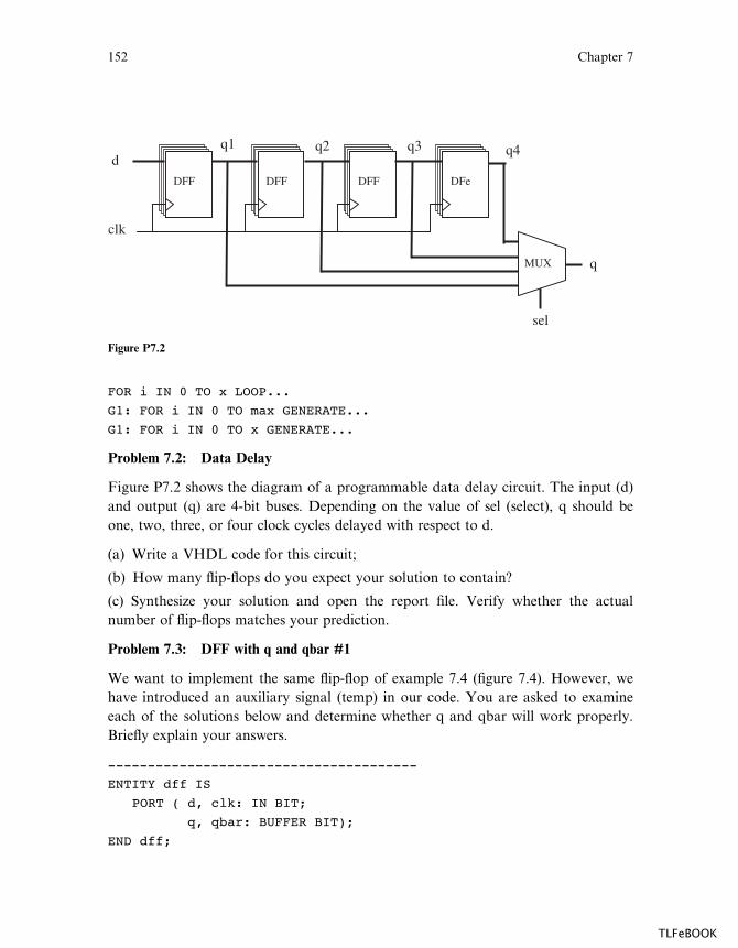
FOR i IN 0 TO x LOOP...
G1: FOR i IN 0 TO max GENERATE...
G1: FOR i IN 0 TO x GENERATE...
Problem 7.2: Data Delay
Figure P7.2 shows the diagram of a programmable data delay circuit. The input (d)
and output (q) are 4-bit buses. Depending on the value of sel (select), q should be
one, two, three, or four clock cycles delayed with respect to d.
(a) Write a VHDL code for this circuit;
(b) How many flip-flops do you expect your solution to contain?
(c) Synthesize your solution and open the report file. Verify whether the actual
number of flip-flops matches your prediction.
Problem 7.3: DFF with q and qbar #1
We want to implement the same flip-flop of example 7.4 (figure 7.4). However, we
have introduced an auxiliary signal (temp) in our code. You are asked to examine
each of the solutions below and determine whether q and qbar will work properly.
Briefly explain your answers.
---------------------------------------
ENTITY dff IS
PORT ( d, clk: IN BIT;
q, qbar: BUFFER BIT);
END dff;
q4q3q2q1
DFF
d
clk
DFF
q
sel
DFeDFF
MUX
Figure P7.2
152 Chapter 7
TLFeBOOK

-------- Solution 1 -------------------
ARCHITECTURE arch1 OF dff IS
SIGNAL temp: BIT;
BEGIN
PROCESS (clk)
BEGIN
IF (clk'EVENT AND clk='1') THEN
temp <= d;
q <= temp;
qbar <= NOT temp;
END IF;
END PROCESS;
END arch1;
-------- Solution 2 -------------------
ARCHITECTURE arch2 OF dff IS
SIGNAL temp: BIT;
BEGIN
PROCESS (clk)
BEGIN
IF (clk'EVENT AND clk='1') THEN
temp <= d;
END IF;
q <= temp;
qbar <= NOT temp;
END PROCESS;
END arch2;
-------- Solution 3 -------------------
ARCHITECTURE arch3 OF dff IS
SIGNAL temp: BIT;
BEGIN
PROCESS (clk)
BEGIN
IF (clk'EVENT AND clk='1') THEN
temp <= d;
END IF;
END PROCESS;
q <= temp;
qbar <= NOT temp;
Signals and Variables 153
TLFeBOOK

END arch3;
---------------------------------------
Problem 7.4: DFF with q and qbar #2
This problem is similar to problem 7.3. However, here we have an auxiliary VARI-
ABLE instead of an auxiliary SIGNAL. You are asked to examine each of the
solutions below and determine whether q and qbar will work as expected. Briefly
explain your answers.
---------------------------------------
ENTITY dff IS
PORT ( d, clk: IN BIT;
q: BUFFER BIT;
qbar: OUT BIT);
END dff;
-------- Solution 1 -------------------
ARCHITECTURE arch1 OF dff IS
BEGIN
PROCESS (clk)
VARIABLE temp: BIT;
BEGIN
IF (clk'EVENT AND clk='1') THEN
temp := d;
q <= temp;
qbar <= NOT temp;
END IF;
END PROCESS;
END arch1;
-------- Solution 2 -------------------
ARCHITECTURE arch2 OF dff IS
BEGIN
PROCESS (clk)
VARIABLE temp: BIT;
BEGIN
IF (clk'EVENT AND clk='1') THEN
temp := d;
q <= temp;
qbar <= NOT q;
154 Chapter 7
TLFeBOOK
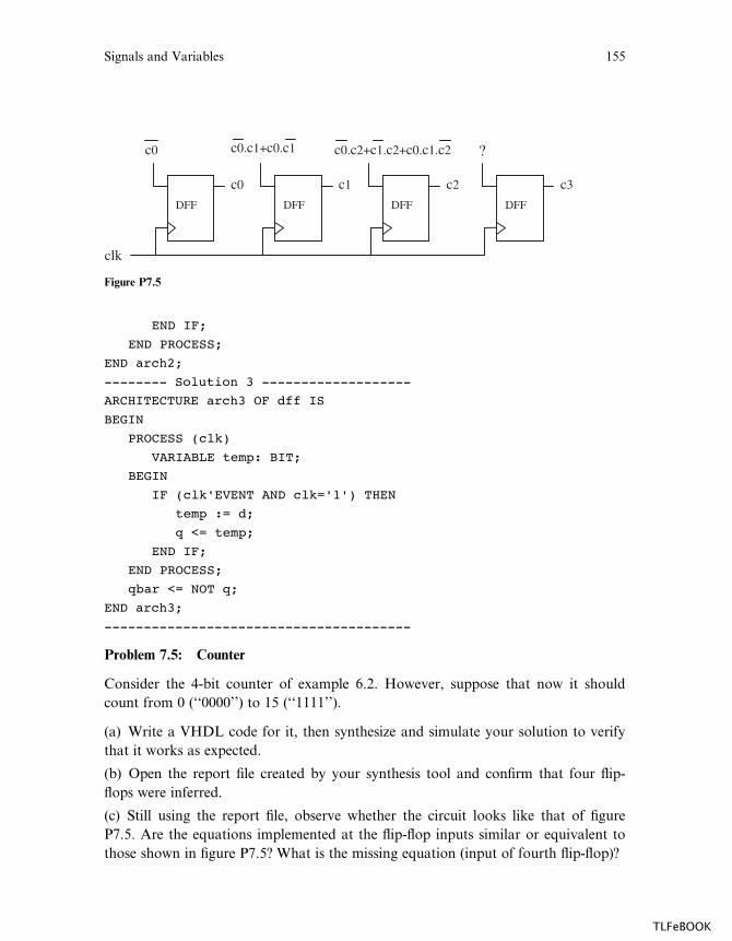
END IF;
END PROCESS;
END arch2;
-------- Solution 3 -------------------
ARCHITECTURE arch3 OF dff IS
BEGIN
PROCESS (clk)
VARIABLE temp: BIT;
BEGIN
IF (clk'EVENT AND clk='1') THEN
temp := d;
q <= temp;
END IF;
END PROCESS;
qbar <= NOT q;
END arch3;
---------------------------------------
Problem 7.5: Counter
Consider the 4-bit counter of example 6.2. However, suppose that now it should
count from 0 (‘‘0000’’) to 15 (‘‘1111’’).
(a) Write a VHDL code for it, then synthesize and simulate your solution to verify
that it works as expected.
(b) Open the report file created by your synthesis tool and confirm that four flip-
flops were inferred.
(c) Still using the report file, observe whether the circuit looks like that of figure
P7.5. Are the equations implemented at the flip-flop inputs similar or equivalent to
those shown in figure P7.5? What is the missing equation (input of fourth flip-flop)?
clk
DFF
c0
c0
DFF
c1
c0.c1+c0.c1
DFF
c2
c0.c2+c1.c2+c0.c1.c2
DFF
?
c3
Figure P7.5
Signals and Variables 155
TLFeBOOK

Problem 7.6: Generic n-by-m Decoder
Let us consider the generic n-by-m decoder presented in example 4.1 (repeated in
figure P7.6). The code presented below, though very compact, contains a flaw in the
assignment ‘‘x<=(sel=>'0', OTHERS=>'1'’’. The reason is that sel is not a locally
stable signal (indeed, it appears in the sensitivity list of the PROCESS). You are
asked to correct the code.
---------------------------------------------
LIBRARY ieee;
USE ieee.std_logic_1164.all;
---------------------------------------------
ENTITY decoder IS
PORT ( ena : IN STD_LOGIC;
sel : IN INTEGER RANGE 0 TO 7;
x : OUT STD_LOGIC_VECTOR (7 DOWNTO 0));
END decoder;
---------------------------------------------
ARCHITECTURE not_ok OF decoder IS
BEGIN
PROCESS (ena, sel)
BEGIN
IF (ena='0') THEN
x <= (OTHERS => '1');
ELSE
x <= (sel=>'0', OTHERS => '1');
END IF;
END PROCESS;
END not_ok;
---------------------------------------------
sel (m-1:0)
ena
x(n-1)x(n-2)…x(1)x(0)
m x nDECODER
Figure P7.6
156 Chapter 7
TLFeBOOK

Problem 7.7: DFF with q and qbar #3
Consider the DFF implemented in solution 2 of example 7.6. We are interested in
examining the number of registers required in its implementation. We already know
that the answer is one. However, as we mentioned in the comments of example 7.6,
even though the synthesizer tells us so, the fitter (place & route) might opt for two
registers in the final (physical) implementation when q and qbar are connected di-
rectly to output pins. This problem deals with this kind of situation.
(a) Compile the code of example 7.6 (solution 2) using Quartus II 3.0 (appendix D).
Select a device from the MAX3000A or Cyclone family. In the synthesis reports,
verify the number of registers inferred and the equations implemented by the syn-
thesizer (confirming the number of flip-flops). Next, repeat these verifications in the
fitter reports (number of registers and equations).
(b) Repeat the procedure above for another device. Select a chip from the
FLEX10K family.
(c) Compile now the code of example 7.6 (solution 2) using ISE 6.1 (appendix B).
Select a device from the XC9500 or CoolRunner II family. After compilation, make
the same verifications described above.
(d) Finally, consider the case when one of the outputs of the flip-flop is not con-
nected directly to a pin. In order to do so, we have introduced a signal called test in
the code below. Repeat all topics above for this new code.
1 ----------------------------------------
2 LIBRARY ieee;
3 USE ieee.std_logic_1164.all;
4 ----------------------------------------
5 ENTITY dff IS
6 PORT ( d, clk, test: IN STD_LOGIC;
7 q: BUFFER STD_LOGIC;
8 qbar: OUT STD_LOGIC);
9 END dff;
10 ----------------------------------------
11 ARCHITECTURE one_dff OF dff IS
12 BEGIN
13 PROCESS (clk)
14 BEGIN
Signals and Variables 157
TLFeBOOK

15 IF (clk'EVENT AND clk='1') THEN
16 q <= d;
17 END IF;
18 END PROCESS;
19 qbar <= NOT q AND test;
20 END one_dff;
21 ----------------------------------------
158 Chapter 7
TLFeBOOK

8 State Machines
Finite state machines (FSM) constitute a special modeling technique for sequential
logic circuits. Such a model can be very helpful in the design of certain types of sys-
tems, particularly those whose tasks form a well-defined sequence (digital controllers,
for example). We start the chapter by reviewing fundamental concepts related to
FSM. We then introduce corresponding VHDL coding techniques, followed by
complete design examples.
8.1 Introduction
Figure 8.1 shows the block diagram of a single-phase state machine. As indicated in
the figure, the lower section contains the sequential logic (flip-flops), while the upper
section contains the combinational logic.
The combinational (upper) section has two inputs, being one pr_state (present
state) and the other the external input proper. It has also two outputs, nx_state (next
state) and the external output proper.
The sequential (lower) section has three inputs (clock, reset, and nx_state), and one
output (pr_state). Since all flip-flops are in this part of the system, clock and reset
must be connected to it.
If the output of the machine depends not only on the present state but also on the
current input, then it is called a Mealy machine. Otherwise, if it depends only on
the current state, it is called a Moore machine. Examples of both will be shown
later.
The separation of the circuit into two sections (figure 8.1) allows the design to be
broken into two parts as well. From a VHDL perspective, it is clear that the lower
part, being sequential, will require a PROCESS, while the upper part, being combi-
national, will not. However, recall that sequential code can implement both types of
logic, combinational as well as sequential. Hence, if desired, the upper part can also
be implemented using a PROCESS.
The signals clock and reset normally appear in the sensitivity list of the lower sec-
tion’s PROCESS (unless reset is synchronous or not used, or WAIT is used instead
of IF). When reset is asserted, pr_state will be set to the system’s initial state. Other-
wise, at the proper clock edge the flip-flops will store nx_state, thus transferring it to
the lower section’s output (pr_state).
One important aspect related to the FSM approach is that, though any sequential
circuit can in principle be modeled as a state machine, this is not always advantageous.
The reason is that the code might become longer, more complex, and more error
prone than in a conventional approach. This is often the case with simple registered
TLFeBOOK

circuits, like counters. As a simple rule of thumb, the FSM approach is advisable in
systems whose tasks constitute a well-structured list so all states can be easily enum-
erated. That is, in a typical state machine implementation, we will encounter, at the
beginning of the ARCHITECTURE, a user-defined enumerated data type, contain-
ing a list of all possible system states. Digital controllers are good examples of such
circuits.
Another important aspect, which was already emphasized at the beginning of
chapter 5, is that not all circuits that possess memory are necessarily sequential.
A RAM (Random Access Memory) was given as an example. In it, the
memory-read operation depends only on the address bits presently applied to the
RAM (current input), with the retrieved value having nothing to do with pre-
vious memory accesses (previous inputs). In such cases, the FSM approach is not
advisable.
8.2 Design Style #1
Several approaches can be conceived to design a FSM. We will describe in detail one
style that is well structured and easily applicable. In it, the design of the lower section
of the state machine (figure 8.1) is completely separated from that of the upper sec-
tion. All states of the machine are always explicitly declared using an enumerated
data type. After introducing such a design style, we will examine it from a data
input
nx_state pr_state
output
reset
clock
Combinational logic
Sequential logic
Figure 8.1Mealy (Moore) state machine diagram.
160 Chapter 8
TLFeBOOK
storage perspective, in order to further understand and refine its construction, which
will lead to design style #2.
Design of the Lower (Sequential) Section
In figure 8.1, the flip-flops are in the lower section, so clock and reset are connected
to it. The other lower section’s input is nx_state (next state), while pr_state (present
state) is its only output. Being the circuit of the lower section sequential, a PROCESS
is required, in which any of the sequential statements (IF, WAIT, CASE, or LOOP,
chapter 6) can be employed.
A typical design template for the lower section is the following:
PROCESS (reset, clock)
BEGIN
IF (reset='1') THEN
pr_state <= state0;
ELSIF (clock'EVENT AND clock='1') THEN
pr_state <= nx_state;
END IF;
END PROCESS;
The code shown above is very simple. It consists of an asynchronous reset, which
determines the initial state of the system (state0), followed by the synchronous stor-
age of nx_state (at the positive transition of clock), which will produce pr_state at the
lower section’s output (figure 8.1). One good thing about this approach is that the
design of the lower section is basically standard.
Another advantage of this design style is that the number of registers is mini-
mum. From section 7.5, we know that the number of flip-flops inferred from the
code above is simply equal to the number of bits needed to encode all states of
the FSM (because the only signal to which a value is assigned at the transition of
another signal is pr_state). Therefore, if the default (binary) encoding style (section
8.4) is used, just d log2ne flip-flops will then be needed, where n is the number of
states.
Design of the Upper (Combinational) Section
In figure 8.1, the upper section is fully combinational, so its code does not need to be
sequential; concurrent code can be used as well. Yet, in the design template shown
below, sequential code was employed, with the CASE statement playing the central
role. In this case, recall that rules 1 and 2 of section 6.10 must be observed.
State Machines 161
TLFeBOOK
PROCESS (input, pr_state)
BEGIN
CASE pr_state IS
WHEN state0 =>
IF (input = ...) THEN
output <= <value>;
nx_state <= state1;
ELSE ...
END IF;
WHEN state1 =>
IF (input = ...) THEN
output <= <value>;
nx_state <= state2;
ELSE ...
END IF;
WHEN state2 =>
IF (input = ...) THEN
output <= <value>;
nx_state <= state2;
ELSE ...
END IF;
...
END CASE;
END PROCESS;
As can be seen, this code is also very simple, and does two things: (a) it assigns the
output value and (b) it establishes the next state. Notice also that it complies with
rules 1 and 2 of section 6.10, relative to the design of combinational circuits using
sequential statements, for all input signals are present in the sensitivity list and all
input/output combinations are specified. Finally, observe that no signal assign-
ment is made at the transition of another signal, so no flip-flops will be inferred
(section 7.5).
State Machine Template for Design Style #1
A complete template is shown below. Notice that, in addition to the two processes
presented above, it also contains a user-defined enumerated data type (here called
state), which lists all possible states of the machine.
162 Chapter 8
TLFeBOOK
LIBRARY ieee;USE ieee.std_logic_1164.all;-----------------------------------------------------ENTITY <entity_name> IS
PORT ( input: IN <data_type>;reset, clock: IN STD_LOGIC;output: OUT <data_type>);
END <entity_name>;-----------------------------------------------------ARCHITECTURE <arch_name> OF <entity_name> IS
TYPE state IS (state0, state1, state2, state3, ...);SIGNAL pr_state, nx_state: state;
BEGIN---------- Lower section: ------------------------PROCESS (reset, clock)BEGIN
IF (reset='1') THENpr_state <= state0;
ELSIF (clock'EVENT AND clock='1') THENpr_state <= nx_state;
END IF;END PROCESS;---------- Upper section: ------------------------PROCESS (input, pr_state)BEGIN
CASE pr_state ISWHEN state0 =>
IF (input = ...) THENoutput <= <value>;nx_state <= state1;
ELSE ...END IF;
WHEN state1 =>IF (input = ...) THEN
output <= <value>;nx_state <= state2;
ELSE ...END IF;
WHEN state2 =>IF (input = ...) THEN
output <= <value>;nx_state <= state3;
ELSE ...END IF;
...END CASE;
END PROCESS;END <arch_name>;
State Machines 163
TLFeBOOK
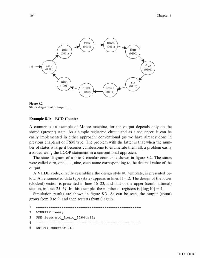
Example 8.1: BCD Counter
A counter is an example of Moore machine, for the output depends only on the
stored (present) state. As a simple registered circuit and as a sequencer, it can be
easily implemented in either approach: conventional (as we have already done in
previous chapters) or FSM type. The problem with the latter is that when the num-
ber of states is large it becomes cumbersome to enumerate them all, a problem easily
avoided using the LOOP statement in a conventional approach.
The state diagram of a 0-to-9 circular counter is shown in figure 8.2. The states
were called zero, one, . . . , nine, each name corresponding to the decimal value of the
output.
A VHDL code, directly resembling the design style #1 template, is presented be-
low. An enumerated data type (state) appears in lines 11–12. The design of the lower
(clocked) section is presented in lines 16–23, and that of the upper (combinational)
section, in lines 25–59. In this example, the number of registers is dlog210e ¼ 4.
Simulation results are shown in figure 8.3. As can be seen, the output (count)
grows from 0 to 9, and then restarts from 0 again.
1 -------------------------------------------------
2 LIBRARY ieee;
3 USE ieee.std_logic_1164.all;
4 -------------------------------------------------
5 ENTITY counter IS
rst zero(0000)
one(0001)
two (0010)
three(0011)
five (0101)
four(0100)
nine (1001)
six(0110)
eight (1000)
seven (0111)
Figure 8.2States diagram of example 8.1.
164 Chapter 8
TLFeBOOK

6 PORT ( clk, rst: IN STD_LOGIC;
7 count: OUT STD_LOGIC_VECTOR (3 DOWNTO 0));
8 END counter;
9 -------------------------------------------------
10 ARCHITECTURE state_machine OF counter IS
11 TYPE state IS (zero, one, two, three, four,
12 five, six, seven, eight, nine);
13 SIGNAL pr_state, nx_state: state;
14 BEGIN
15 ------------- Lower section: -----------------
16 PROCESS (rst, clk)
17 BEGIN
18 IF (rst='1') THEN
19 pr_state <= zero;
20 ELSIF (clk'EVENT AND clk='1') THEN
21 pr_state <= nx_state;
22 END IF;
23 END PROCESS;
24 ------------- Upper section: -----------------
25 PROCESS (pr_state)
26 BEGIN
27 CASE pr_state IS
28 WHEN zero =>
29 count <= "0000";
30 nx_state <= one;
31 WHEN one =>
32 count <= "0001";
33 nx_state <= two;
Figure 8.3Simulation results of example 8.1.
State Machines 165
TLFeBOOK
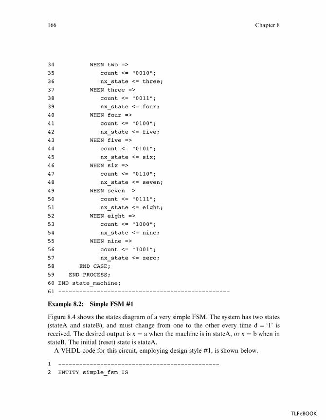
34 WHEN two =>
35 count <= "0010";
36 nx_state <= three;
37 WHEN three =>
38 count <= "0011";
39 nx_state <= four;
40 WHEN four =>
41 count <= "0100";
42 nx_state <= five;
43 WHEN five =>
44 count <= "0101";
45 nx_state <= six;
46 WHEN six =>
47 count <= "0110";
48 nx_state <= seven;
49 WHEN seven =>
50 count <= "0111";
51 nx_state <= eight;
52 WHEN eight =>
53 count <= "1000";
54 nx_state <= nine;
55 WHEN nine =>
56 count <= "1001";
57 nx_state <= zero;
58 END CASE;
59 END PROCESS;
60 END state_machine;
61 -------------------------------------------------
Example 8.2: Simple FSM #1
Figure 8.4 shows the states diagram of a very simple FSM. The system has two states
(stateA and stateB), and must change from one to the other every time d ¼ ‘1’ is
received. The desired output is x ¼ a when the machine is in stateA, or x ¼ b when in
stateB. The initial (reset) state is stateA.
A VHDL code for this circuit, employing design style #1, is shown below.
1 ----------------------------------------------
2 ENTITY simple_fsm IS
166 Chapter 8
TLFeBOOK
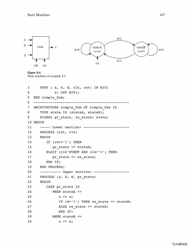
3 PORT ( a, b, d, clk, rst: IN BIT;
4 x: OUT BIT);
5 END simple_fsm;
6 ----------------------------------------------
7 ARCHITECTURE simple_fsm OF simple_fsm IS
8 TYPE state IS (stateA, stateB);
9 SIGNAL pr_state, nx_state: state;
10 BEGIN
11 ----- Lower section: ----------------------
12 PROCESS (rst, clk)
13 BEGIN
14 IF (rst='1') THEN
15 pr_state <= stateA;
16 ELSIF (clk'EVENT AND clk='1') THEN
17 pr_state <= nx_state;
18 END IF;
19 END PROCESS;
20 ---------- Upper section: -----------------
21 PROCESS (a, b, d, pr_state)
22 BEGIN
23 CASE pr_state IS
24 WHEN stateA =>
25 x <= a;
26 IF (d='1') THEN nx_state <= stateB;
27 ELSE nx_state <= stateA;
28 END IF;
29 WHEN stateB =>
30 x <= b;
a
b
d
xFSM
clk rst rst
d=1
d=1
d=0stateA (x=a)
stateB (x=b) d=0
Figure 8.4State machine of example 8.1.
State Machines 167
TLFeBOOK
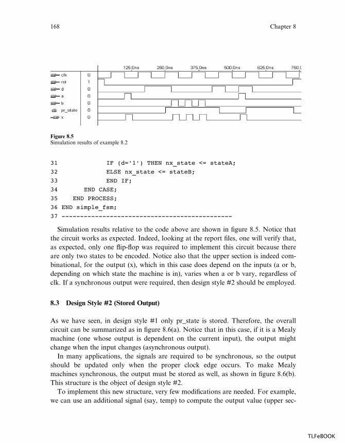
31 IF (d='1') THEN nx_state <= stateA;
32 ELSE nx_state <= stateB;
33 END IF;
34 END CASE;
35 END PROCESS;
36 END simple_fsm;
37 ----------------------------------------------
Simulation results relative to the code above are shown in figure 8.5. Notice that
the circuit works as expected. Indeed, looking at the report files, one will verify that,
as expected, only one flip-flop was required to implement this circuit because there
are only two states to be encoded. Notice also that the upper section is indeed com-
binational, for the output (x), which in this case does depend on the inputs (a or b,
depending on which state the machine is in), varies when a or b vary, regardless of
clk. If a synchronous output were required, then design style #2 should be employed.
8.3 Design Style #2 (Stored Output)
As we have seen, in design style #1 only pr_state is stored. Therefore, the overall
circuit can be summarized as in figure 8.6(a). Notice that in this case, if it is a Mealy
machine (one whose output is dependent on the current input), the output might
change when the input changes (asynchronous output).
In many applications, the signals are required to be synchronous, so the output
should be updated only when the proper clock edge occurs. To make Mealy
machines synchronous, the output must be stored as well, as shown in figure 8.6(b).
This structure is the object of design style #2.
To implement this new structure, very few modifications are needed. For example,
we can use an additional signal (say, temp) to compute the output value (upper sec-
Figure 8.5Simulation results of example 8.2
168 Chapter 8
TLFeBOOK
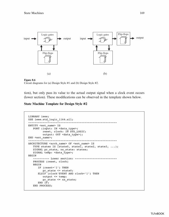
tion), but only pass its value to the actual output signal when a clock event occurs
(lower section). These modifications can be observed in the template shown below.
State Machine Template for Design Style #2
LIBRARY ieee;USE ieee.std_logic_1164.all;-------------------------------------------------------ENTITY <ent_name> IS
PORT (input: IN <data_type>;reset, clock: IN STD_LOGIC;output: OUT <data_type>);
END <ent_name>;-------------------------------------------------------ARCHITECTURE <arch_name> OF <ent_name> IS
TYPE states IS (state0, state1, state2, state3, ...);SIGNAL pr_state, nx_state: states;SIGNAL temp: <data_type>;
BEGIN---------- Lower section: --------------------------PROCESS (reset, clock)BEGIN
IF (reset='1') THENpr_state <= state0;
ELSIF (clock'EVENT AND clock='1') THENoutput <= temp;pr_state <= nx_state;
END IF;END PROCESS;
(a) (b)
input output Logic gates
Flip-flops
Flip-flops
input output Logic gates
Flip-flops
Figure 8.6Circuit diagrams for (a) Design Style #1 and (b) Design Style #2.
State Machines 169
TLFeBOOK
---------- Upper section: --------------------------PROCESS (pr_state)BEGIN
CASE pr_state ISWHEN state0 =>
temp <= <value>;IF (condition) THEN nx_state <= state1;...END IF;
WHEN state1 =>temp <= <value>;IF (condition) THEN nx_state <= state2;...END IF;
WHEN state2 =>temp <= <value>;IF (condition) THEN nx_state <= state3;...END IF;
...END CASE;
END PROCESS;END <arch_name>;
Comparing the template of design style #2 with that of design style #1, we verify
that the only di¤erences are those related to the introduction of the internal signal
temp. This signal will cause the output of the state machine to be stored, for its value
is passed to the output only when clk’EVENT occurs.
Example 8.3: Simple FSM #2
Let us consider the design of example 8.2 once again. However, let us say that now
we want the output to be synchronous (to change only when clock rises). Since this is
a Mealy machine, design style #2 is required.
1 ----------------------------------------------
2 ENTITY simple_fsm IS
3 PORT ( a, b, d, clk, rst: IN BIT;
4 x: OUT BIT);
5 END simple_fsm;
6 ----------------------------------------------
7 ARCHITECTURE simple_fsm OF simple_fsm IS
8 TYPE state IS (stateA, stateB);
9 SIGNAL pr_state, nx_state: state;
10 SIGNAL temp: BIT;
170 Chapter 8
TLFeBOOK
11 BEGIN
12 ----- Lower section: ----------------------
13 PROCESS (rst, clk)
14 BEGIN
15 IF (rst='1') THEN
16 pr_state <= stateA;
17 ELSIF (clk'EVENT AND clk='1') THEN
18 x <= temp;
19 pr_state <= nx_state;
20 END IF;
21 END PROCESS;
22 ---------- Upper section: -----------------
23 PROCESS (a, b, d, pr_state)
24 BEGIN
25 CASE pr_state IS
26 WHEN stateA =>
27 temp <= a;
28 IF (d='1') THEN nx_state <= stateB;
29 ELSE nx_state <= stateA;
30 END IF;
31 WHEN stateB =>
32 temp <= b;
33 IF (d='1') THEN nx_state <= stateA;
34 ELSE nx_state <= stateB;
35 END IF;
36 END CASE;
37 END PROCESS;
38 END simple_fsm;
39 ----------------------------------------------
Looking at the report files produced by the compiler, we observe that two flip-flops
were now inferred, one to encode the states of the machine, and the other to store the
output.
Simulation results are shown in figure 8.7. Recall that when a signal is stored, its
value will necessarily remain static between two consecutive clock edges. Therefore,
if the input (a or b in the example above) changes during this interval, the change
might not be observed by the circuit; moreover, when observed, it will be delayed
with respect to the input (which is proper of synchronous circuits).
State Machines 171
TLFeBOOK

Example 8.4: String Detector
We want to design a circuit that takes as input a serial bit stream and outputs a ‘1’
whenever the sequence ‘‘111’’ occurs. Overlaps must also be considered, that is, if . . .
0111110 . . . occurs, than the output should remain active for three consecutive clock
cycles.
The state diagram of our machine is shown in figure 8.8. There are four states,
which we called zero, one, two, and three, with the name corresponding to the
number of consecutive ‘1’s detected. The solution shown below utilizes design style
#1.
Figure 8.7Simulation results of example 8.3.
d=0
d=1
d=0
d=0
d=1d=0
d=1d=1
rstzero(q=0)
three(q=1)
two (q=0)
one(q=0)
Figure 8.8States diagram for example 8.4.
172 Chapter 8
TLFeBOOK
1 --------------------------------------------
2 LIBRARY ieee;
3 USE ieee.std_logic_1164.all;
4 --------------------------------------------
5 ENTITY string_detector IS
6 PORT ( d, clk, rst: IN BIT;
7 q: OUT BIT);
8 END string_detector;
9 --------------------------------------------
10 ARCHITECTURE my_arch OF string_detector IS
11 TYPE state IS (zero, one, two, three);
12 SIGNAL pr_state, nx_state: state;
13 BEGIN
14 ----- Lower section: --------------------
15 PROCESS (rst, clk)
16 BEGIN
17 IF (rst='1') THEN
18 pr_state <= zero;
19 ELSIF (clk'EVENT AND clk='1') THEN
20 pr_state <= nx_state;
21 END IF;
22 END PROCESS;
23 ---------- Upper section: ---------------
24 PROCESS (d, pr_state)
25 BEGIN
26 CASE pr_state IS
27 WHEN zero =>
28 q <= '0';
29 IF (d='1') THEN nx_state <= one;
30 ELSE nx_state <= zero;
31 END IF;
32 WHEN one =>
33 q <= '0';
34 IF (d='1') THEN nx_state <= two;
35 ELSE nx_state <= zero;
36 END IF;
37 WHEN two =>
38 q <= '0';
39 IF (d='1') THEN nx_state <= three;
State Machines 173
TLFeBOOK

40 ELSE nx_state <= zero;
41 END IF;
42 WHEN three =>
43 q <= '1';
44 IF (d='0') THEN nx_state <= zero;
45 ELSE nx_state <= three;
46 END IF;
47 END CASE;
48 END PROCESS;
49 END my_arch;
50 --------------------------------------------
Notice that in this example the output does not depend on the current input. This
fact can be observed in lines 28, 33, 38, and 43 of the code above, which show that all
assignments to q are unconditional (that is, do not depend on d). Therefore, the
output is automatically synchronous (a Moore machine), so the use of design style
#2 is unnecessary. The circuit requires two flip-flops, which encode the four states of
the state machine, from which q is computed.
Simulation results are shown in figure 8.9. As can be seen, the data sequence
d ¼ ‘‘011101100’’ was applied to the circuit, resulting the response q ¼ ‘‘000100000’’
at the output.
Example 8.5: Tra‰c Light Controller (TLC)
As mentioned earlier, digital controllers are good examples of circuits that can be
e‰ciently implemented when modeled as state machines. In the present example, we
want to design a TLC with the characteristics summarized in the table of figure 8.10,
that is:
� Three modes of operation: Regular, Test, and Standby.
� Regular mode: four states, each with an independent, programmable time, passed
to the circuit by means of a CONSTANT.
� Test mode: allows all pre-programmed times to be overwritten (by a manual
switch) with a small value, such that the system can be easily tested during mainte-
nance (1 second per state). This value should also be programmable and passed to
the circuit using a CONSTANT.
� Standby mode: if set (by a sensor accusing malfunctioning, for example, or a man-
ual switch) the system should activate the yellow lights in both directions and remain
so while the standby signal is active.
� Assume that a 60 Hz clock (obtained from the power line itself ) is available.
174 Chapter 8
TLFeBOOK
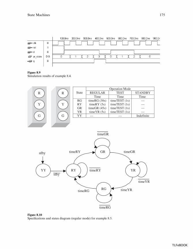
Figure 8.9Simulation results of example 8.4.
Operation ModeREGULAR TEST STANDBYState
Time Time TimeRG RYGR YR
timeRG (30s) timeRY (5s)
timeGR (45s) timeYR (5s)
timeTEST (1s) timeTEST (1s) timeTEST (1s) timeTEST (1s)
------------
YY --- --- IndefiniteG
Y
R
G
Y
R
RY
stby GR
YY YR
RG
stby
timeGR
timeYR
timeRG
timeRY
timeYR
timeGR
timeRG
timeRY
Figure 8.10Specifications and states diagram (regular mode) for example 8.5.
State Machines 175
TLFeBOOK

Here, design style #1 can be employed, as shown in the code below.
1 -------------------------------------------------
2 LIBRARY ieee;
3 USE ieee.std_logic_1164.all;
4 -------------------------------------------------
5 ENTITY tlc IS
6 PORT ( clk, stby, test: IN STD_LOGIC;
7 r1, r2, y1, y2, g1, g2: OUT STD_LOGIC);
8 END tlc;
9 -------------------------------------------------
10 ARCHITECTURE behavior OF tlc IS
11 CONSTANT timeMAX : INTEGER := 2700;
12 CONSTANT timeRG : INTEGER := 1800;
13 CONSTANT timeRY : INTEGER := 300;
14 CONSTANT timeGR : INTEGER := 2700;
15 CONSTANT timeYR : INTEGER := 300;
16 CONSTANT timeTEST : INTEGER := 60;
17 TYPE state IS (RG, RY, GR, YR, YY);
18 SIGNAL pr_state, nx_state: state;
19 SIGNAL time : INTEGER RANGE 0 TO timeMAX;
20 BEGIN
21 -------- Lower section of state machine: ----
22 PROCESS (clk, stby)
23 VARIABLE count : INTEGER RANGE 0 TO timeMAX;
24 BEGIN
25 IF (stby='1') THEN
26 pr_state <= YY;
27 count := 0;
28 ELSIF (clk'EVENT AND clk='1') THEN
29 count := count + 1;
30 IF (count = time) THEN
31 pr_state <= nx_state;
32 count := 0;
33 END IF;
34 END IF;
35 END PROCESS;
176 Chapter 8
TLFeBOOK
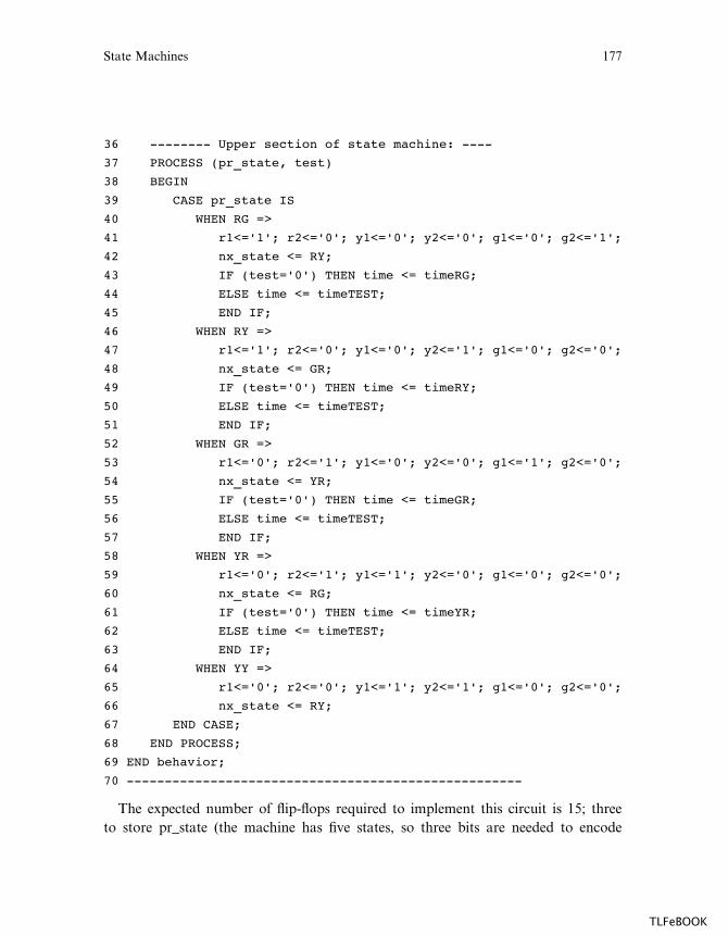
36 -------- Upper section of state machine: ----
37 PROCESS (pr_state, test)
38 BEGIN
39 CASE pr_state IS
40 WHEN RG =>
41 r1<='1'; r2<='0'; y1<='0'; y2<='0'; g1<='0'; g2<='1';
42 nx_state <= RY;
43 IF (test='0') THEN time <= timeRG;
44 ELSE time <= timeTEST;
45 END IF;
46 WHEN RY =>
47 r1<='1'; r2<='0'; y1<='0'; y2<='1'; g1<='0'; g2<='0';
48 nx_state <= GR;
49 IF (test='0') THEN time <= timeRY;
50 ELSE time <= timeTEST;
51 END IF;
52 WHEN GR =>
53 r1<='0'; r2<='1'; y1<='0'; y2<='0'; g1<='1'; g2<='0';
54 nx_state <= YR;
55 IF (test='0') THEN time <= timeGR;
56 ELSE time <= timeTEST;
57 END IF;
58 WHEN YR =>
59 r1<='0'; r2<='1'; y1<='1'; y2<='0'; g1<='0'; g2<='0';
60 nx_state <= RG;
61 IF (test='0') THEN time <= timeYR;
62 ELSE time <= timeTEST;
63 END IF;
64 WHEN YY =>
65 r1<='0'; r2<='0'; y1<='1'; y2<='1'; g1<='0'; g2<='0';
66 nx_state <= RY;
67 END CASE;
68 END PROCESS;
69 END behavior;
70 ----------------------------------------------------
The expected number of flip-flops required to implement this circuit is 15; three
to store pr_state (the machine has five states, so three bits are needed to encode
State Machines 177
TLFeBOOK
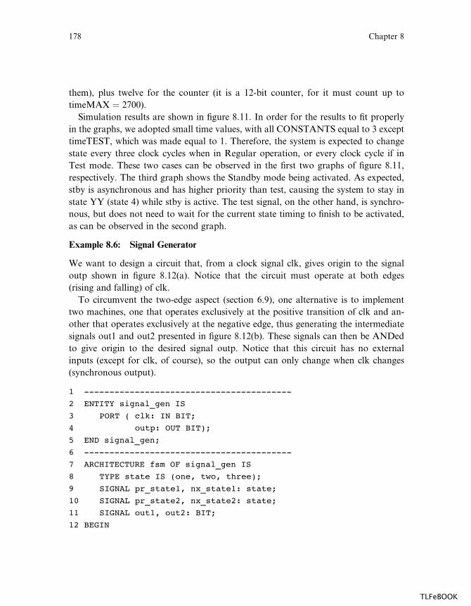
them), plus twelve for the counter (it is a 12-bit counter, for it must count up to
timeMAX ¼ 2700).
Simulation results are shown in figure 8.11. In order for the results to fit properly
in the graphs, we adopted small time values, with all CONSTANTS equal to 3 except
timeTEST, which was made equal to 1. Therefore, the system is expected to change
state every three clock cycles when in Regular operation, or every clock cycle if in
Test mode. These two cases can be observed in the first two graphs of figure 8.11,
respectively. The third graph shows the Standby mode being activated. As expected,
stby is asynchronous and has higher priority than test, causing the system to stay in
state YY (state 4) while stby is active. The test signal, on the other hand, is synchro-
nous, but does not need to wait for the current state timing to finish to be activated,
as can be observed in the second graph.
Example 8.6: Signal Generator
We want to design a circuit that, from a clock signal clk, gives origin to the signal
outp shown in figure 8.12(a). Notice that the circuit must operate at both edges
(rising and falling) of clk.
To circumvent the two-edge aspect (section 6.9), one alternative is to implement
two machines, one that operates exclusively at the positive transition of clk and an-
other that operates exclusively at the negative edge, thus generating the intermediate
signals out1 and out2 presented in figure 8.12(b). These signals can then be ANDed
to give origin to the desired signal outp. Notice that this circuit has no external
inputs (except for clk, of course), so the output can only change when clk changes
(synchronous output).
1 -----------------------------------------
2 ENTITY signal_gen IS
3 PORT ( clk: IN BIT;
4 outp: OUT BIT);
5 END signal_gen;
6 -----------------------------------------
7 ARCHITECTURE fsm OF signal_gen IS
8 TYPE state IS (one, two, three);
9 SIGNAL pr_state1, nx_state1: state;
10 SIGNAL pr_state2, nx_state2: state;
11 SIGNAL out1, out2: BIT;
12 BEGIN
178 Chapter 8
TLFeBOOK
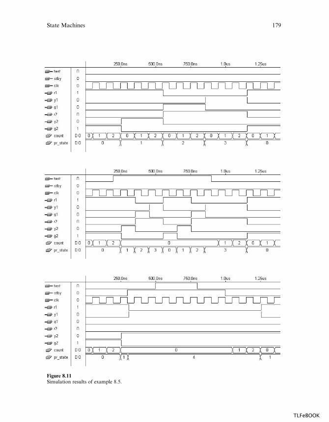
Figure 8.11Simulation results of example 8.5.
State Machines 179
TLFeBOOK
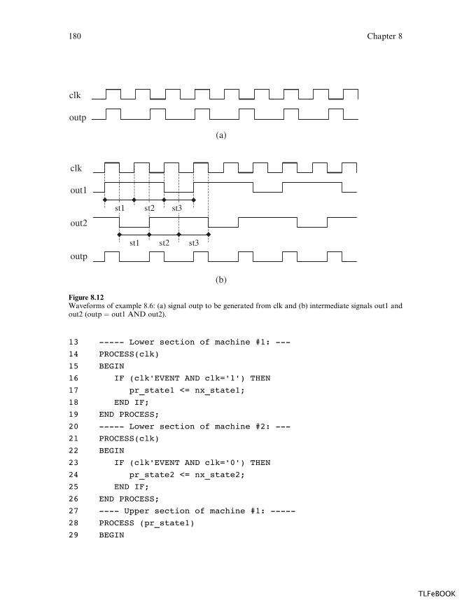
13 ----- Lower section of machine #1: ---
14 PROCESS(clk)
15 BEGIN
16 IF (clk'EVENT AND clk='1') THEN
17 pr_state1 <= nx_state1;
18 END IF;
19 END PROCESS;
20 ----- Lower section of machine #2: ---
21 PROCESS(clk)
22 BEGIN
23 IF (clk'EVENT AND clk='0') THEN
24 pr_state2 <= nx_state2;
25 END IF;
26 END PROCESS;
27 ---- Upper section of machine #1: -----
28 PROCESS (pr_state1)
29 BEGIN
(a)
(b)
clk
outp
st1 st2 st3
clk
out1
out2
outp
st1 st2 st3
Figure 8.12Waveforms of example 8.6: (a) signal outp to be generated from clk and (b) intermediate signals out1 andout2 (outp ¼ out1 AND out2).
180 Chapter 8
TLFeBOOK
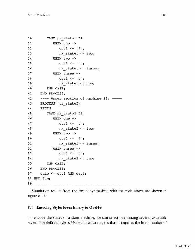
30 CASE pr_state1 IS
31 WHEN one =>
32 out1 <= '0';
33 nx_state1 <= two;
34 WHEN two =>
35 out1 <= '1';
36 nx_state1 <= three;
37 WHEN three =>
38 out1 <= '1';
39 nx_state1 <= one;
40 END CASE;
41 END PROCESS;
42 ---- Upper section of machine #2: -----
43 PROCESS (pr_state2)
44 BEGIN
45 CASE pr_state2 IS
46 WHEN one =>
47 out2 <= '1';
48 nx_state2 <= two;
49 WHEN two =>
50 out2 <= '0';
51 nx_state2 <= three;
52 WHEN three =>
53 out2 <= '1';
54 nx_state2 <= one;
55 END CASE;
56 END PROCESS;
57 outp <= out1 AND out2;
58 END fsm;
59 ------------------------------------------
Simulation results from the circuit synthesized with the code above are shown in
figure 8.13.
8.4 Encoding Style: From Binary to OneHot
To encode the states of a state machine, we can select one among several available
styles. The default style is binary. Its advantage is that it requires the least number of
State Machines 181
TLFeBOOK
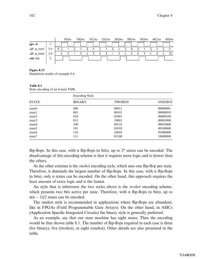
flip-flops. In this case, with n flip-flops (n bits), up to 2n states can be encoded. The
disadvantage of this encoding scheme is that it requires more logic and is slower than
the others.
At the other extreme is the onehot encoding style, which uses one flip-flop per state.
Therefore, it demands the largest number of flip-flops. In this case, with n flip-flops
(n bits), only n states can be encoded. On the other hand, this approach requires the
least amount of extra logic and is the fastest.
An style that is inbetween the two styles above is the twohot encoding scheme,
which presents two bits active per state. Therefore, with n flip-flops (n bits), up to
n(n� 1)/2 states can be encoded.
The onehot style is recommended in applications where flip-flops are abundant,
like in FPGAs (Field Programmable Gate Arrays). On the other hand, in ASICs
(Application Specific Integrated Circuits) the binary style is generally preferred.
As an example, say that our state machine has eight states. Then the encoding
would be that shown table 8.1. The number of flip-flops required in each case is three
(for binary), five (twohot), or eight (onehot). Other details are also presented in the
table.
Figure 8.13Simulation results of example 8.6.
Table 8.1State encoding of an 8-state FSM.
Encoding Style
STATE BINARY TWOHOT ONEHOT
state0 000 00011 00000001
state1 001 00101 00000010
state2 010 01001 00000100
state3 011 10001 00001000
state4 100 00110 00010000
state5 101 01010 00100000
state6 110 10010 01000000
state7 111 01100 10000000
182 Chapter 8
TLFeBOOK
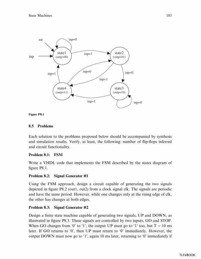
8.5 Problems
Each solution to the problems proposed below should be accompanied by synthesis
and simulation results. Verify, at least, the following: number of flip-flops inferred
and circuit functionality.
Problem 8.1: FSM
Write a VHDL code that implements the FSM described by the states diagram of
figure P8.1.
Problem 8.2: Signal Generator #1
Using the FSM approach, design a circuit capable of generating the two signals
depicted in figure P8.2 (out1, out2) from a clock signal clk. The signals are periodic
and have the same period. However, while one changes only at the rising edge of clk,
the other has changes at both edges.
Problem 8.3: Signal Generator #2
Design a finite state machine capable of generating two signals, UP and DOWN, as
illustrated in figure P8.3. These signals are controlled by two inputs, GO and STOP.
When GO changes from ‘0’ to ‘1’, the output UP must go to ‘1’ too, but T ¼ 10 ms
later. If GO returns to ‘0’, then UP must return to ‘0’ immediately. However, the
output DOWN must now go to ‘1’, again 10 ms later, returning to ‘0’ immediately if
inp=0
inp=0
state1(outp=00)
state4(outp=11)
state3(outp=10)
state2(outp=01)
rst
inp
inp=1
inp=1
inp=1
inp=1
inp=0
inp=0
Figure P8.1
State Machines 183
TLFeBOOK
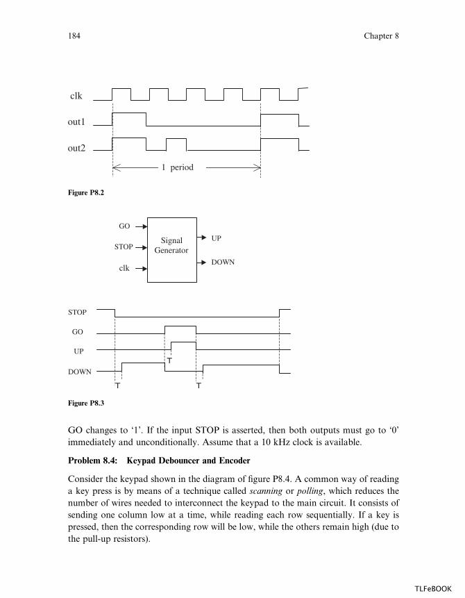
GO changes to ‘1’. If the input STOP is asserted, then both outputs must go to ‘0’
immediately and unconditionally. Assume that a 10 kHz clock is available.
Problem 8.4: Keypad Debouncer and Encoder
Consider the keypad shown in the diagram of figure P8.4. A common way of reading
a key press is by means of a technique called scanning or polling, which reduces the
number of wires needed to interconnect the keypad to the main circuit. It consists of
sending one column low at a time, while reading each row sequentially. If a key is
pressed, then the corresponding row will be low, while the others remain high (due to
the pull-up resistors).
clk
out1
out2
1 period
Figure P8.2
GO
STOP
clk
UP
DOWN
Signal Generator
STOP
GO
UP
DOWN T
T T
Figure P8.3
184 Chapter 8
TLFeBOOK
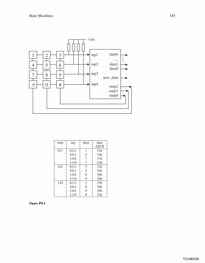
outp inp digit dataASCII
011 0111 1011 1101 1110
147*
31h34h37h2Ah
101 0111 1011 1101 1110
2580
32h35h38h30h
110 0111 1011 1101 1110
369#
33h36h39h23h
1
4
7
2
5
8
3
6
9
* 0 #
inp1
inp2
inp3
inp4
VDD
data6 ...
data1data0
new_data
outp2outp1outp0
Figure P8.4
State Machines 185
TLFeBOOK
Encoding: Each digit must be encoded using the ASCII code (7 bits, with the cor-
responding hexadecimal values listed in the table of figure P8.4). When a new reading
is available at the output, the new_data bit should be set to ‘1’. This will avoid
interpreting a key pressed for a long time as a long series of the same character.
Debouncing: A problem inherent to mechanical switches is switch bounces, which
occur before a firm contact is finally established. The settling generally takes up to a
few milliseconds. Therefore, the choice of the clock frequency is very important. You
are asked to choose it such that at least three readings occur in a 5 ms interval. Thus
the new_data bit should be turned high only when the same result is obtained in all
consecutive readings within a 5 ms interval.
Problem 8.5: Tra‰c Light Controller
Using your synthesis tool plus a CPLD/FPGA development kit, implement the TLC
of example 8.5. Verify, in the report files generated by your software, which pins of
the chip were assigned to the inputs (clk, stby, test) and to the outputs (r1, y1, g1, r2,
y2, g2). Then make the following physical connections in your board:
� a 60 Hz square wave signal (from a signal generator), with the appropriate logic
levels, to the clk pin.
� a VDD/GND switch to pin stby.
� a VDD/GND switch to pin test.
� an LED (red, if possible), with a 330-1kohm series resistor, to pin r1 (resistor con-
nected between r1 and the anode of the LED, and cathode connected to GND).
� an LED (yellow, if possible) to pin y1, with a series resistor like above.
� an LED (green, if possible) to pin g1, with a series resistor like above.
� finally, install other 3 LEDs, like those above, for r2, y2, and g2.
Now download the program file from your PC to the development kit and verify
the operation of the TLC. Play with the switches in order to test all modes of opera-
tion. You can also increase the clock frequency to speed up the transition from red to
yellow, etc.
Problem 8.6: Signal Generator #3
Solve problem 8.2 without using the finite state machine approach.
Problem 8.7: Signal Generator #4
Solve example 8.6 without using the FSM approach.
For further work is this area, see problems 9.3, 9.4, and 9.6 of chapter 9.
186 Chapter 8
TLFeBOOK
9 Additional Circuit Designs
In the preceding chapters, we saw a series of complete design examples utilizing
VHDL code. Each design included:
� Top-level diagram of the circuit, with description;
� Review of basic concepts whenever necessary;
� Complete VHDL code;
� Simulation results; and
� Additional comments when needed.
This chapter concludes Part I of the book. In it, a series of additional design
examples are presented. These examples, like all the other designs shown so far, are
also at the circuit level (that is, self-contained in the main code). In Part II, we will do
the same; that is, we will conclude Part II with a chapter containing additional system
design examples.
The designs presented in this chapter are the following:
� Barrel shifter (section 9.1)
� Signed and unsigned comparators (section 9.2)
� Carry ripple and carry look ahead adders (section 9.3)
� Fixed-point division (section 9.4)
� Vending machine controller (section 9.5)
� Serial data receiver (section 9.6)
� Parallel-to-serial converter (section 9.7)
� Playing with a SSD (section 9.8)
� Signal generators (section 9.9)
� Memories (section 9.10)
� Finally, a list of problems is also included (section 9.11).
Note: A complete list of all designs presented in the book is shown in section 1.5.
9.1 Barrel Shifter
The diagram of a barrel shifter is shown in figure 9.1. The input is an 8-bit vector.
The output is a shifted version of the input, with the amount of shift defined by the
‘‘shift’’ input (from 0 to 7). The circuit consists of three individual barrel shifters,
each similar to that seen in example 6.9. Notice that the first barrel has only one ‘0’
TLFeBOOK
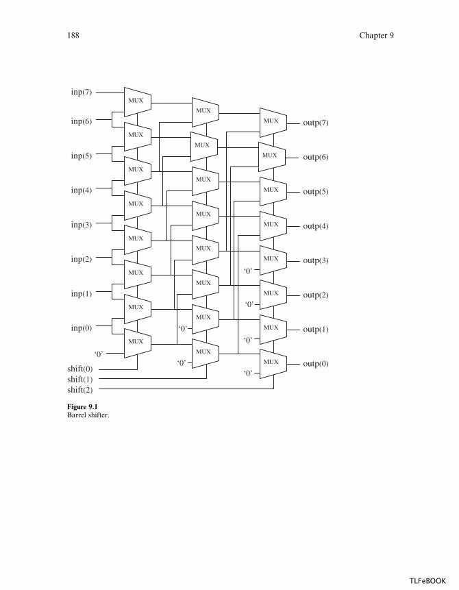
outp(7)
outp(6)
outp(5)
outp(4)
outp(3)
outp(2)
outp(1)
outp(0)shift(0)shift(1)shift(2)
‘0’
inp(7)MUX
inp(6)
MUX
inp(5)
MUX
inp(4)
MUX
inp(3)
MUX
inp(2)
MUX
inp(1)
MUX
inp(0)
MUX
‘0’
MUX
MUX
MUX
MUX
MUX
MUX
MUX
MUX
‘0’
‘0’
MUX
MUX
MUX
MUX
MUX
MUX
MUX
MUX
‘0’
‘0’
‘0’
Figure 9.1Barrel shifter.
188 Chapter 9
TLFeBOOK
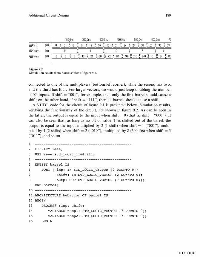
connected to one of the multiplexers (bottom left corner), while the second has two,
and the third has four. For larger vectors, we would just keep doubling the number
of ‘0’ inputs. If shift ¼ ‘‘001’’, for example, then only the first barrel should cause a
shift; on the other hand, if shift ¼ ‘‘111’’, then all barrels should cause a shift.
A VHDL code for the circuit of figure 9.1 is presented below. Simulation results,
verifying the functionality of the circuit, are shown in figure 9.2. As can be seen in
the latter, the output is equal to the input when shift ¼ 0 (that is, shift ¼ ‘‘000’’). It
can also be seen that, as long as no bit of value ‘1’ is shifted out of the barrel, the
output is equal to the input multiplied by 2 (1 shift) when shift ¼ 1 (‘‘001’’), multi-
plied by 4 (2 shifts) when shift ¼ 2 (‘‘010’’), multiplied by 8 (3 shifts) when shift ¼ 3
(‘‘011’’), and so on.
1 ---------------------------------------------
2 LIBRARY ieee;
3 USE ieee.std_logic_1164.all;
4 ---------------------------------------------
5 ENTITY barrel IS
6 PORT ( inp: IN STD_LOGIC_VECTOR (7 DOWNTO 0);
7 shift: IN STD_LOGIC_VECTOR (2 DOWNTO 0);
8 outp: OUT STD_LOGIC_VECTOR (7 DOWNTO 0));
9 END barrel;
10 ---------------------------------------------
11 ARCHITECTURE behavior OF barrel IS
12 BEGIN
13 PROCESS (inp, shift)
14 VARIABLE temp1: STD_LOGIC_VECTOR (7 DOWNTO 0);
15 VARIABLE temp2: STD_LOGIC_VECTOR (7 DOWNTO 0);
16 BEGIN
Figure 9.2Simulation results from barrel shifter of figure 9.1.
Additional Circuit Designs 189
TLFeBOOK
17 ---- 1st shifter -----
18 IF (shift(0)='0') THEN
19 temp1 := inp;
20 ELSE
21 temp1(0) := '0';
22 FOR i IN 1 TO inp'HIGH LOOP
23 temp1(i) := inp(i-1);
24 END LOOP;
25 END IF;
26 ---- 2nd shifter -----
27 IF (shift(1)='0') THEN
28 temp2 := temp1;
29 ELSE
30 FOR i IN 0 TO 1 LOOP
31 temp2(i) := '0';
32 END LOOP;
33 FOR i IN 2 TO inp'HIGH LOOP
34 temp2(i) := temp1(i-2);
35 END LOOP;
36 END IF;
37 ---- 3rd shifter -----
38 IF (shift(2)='0') THEN
39 outp <= temp2;
40 ELSE
41 FOR i IN 0 TO 3 LOOP
42 outp(i) <= '0';
43 END LOOP;
44 FOR i IN 4 TO inp'HIGH LOOP
45 outp(i) <= temp2(i-4);
46 END LOOP;
47 END IF;
48 END PROCESS;
49 END behavior;
50 ---------------------------------------------
190 Chapter 9
TLFeBOOK
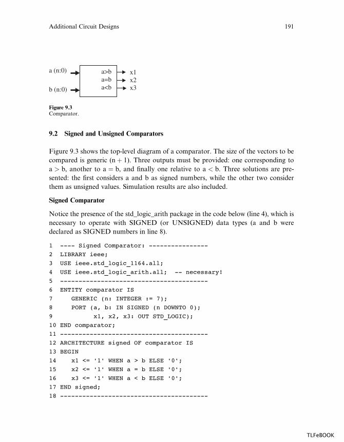
9.2 Signed and Unsigned Comparators
Figure 9.3 shows the top-level diagram of a comparator. The size of the vectors to be
compared is generic (nþ 1). Three outputs must be provided: one corresponding to
a > b, another to a ¼ b, and finally one relative to a < b. Three solutions are pre-
sented: the first considers a and b as signed numbers, while the other two consider
them as unsigned values. Simulation results are also included.
Signed Comparator
Notice the presence of the std_logic_arith package in the code below (line 4), which is
necessary to operate with SIGNED (or UNSIGNED) data types (a and b were
declared as SIGNED numbers in line 8).
1 ---- Signed Comparator: ----------------
2 LIBRARY ieee;
3 USE ieee.std_logic_1164.all;
4 USE ieee.std_logic_arith.all; -- necessary!
5 ----------------------------------------
6 ENTITY comparator IS
7 GENERIC (n: INTEGER := 7);
8 PORT (a, b: IN SIGNED (n DOWNTO 0);
9 x1, x2, x3: OUT STD_LOGIC);
10 END comparator;
11 ----------------------------------------
12 ARCHITECTURE signed OF comparator IS
13 BEGIN
14 x1 <= '1' WHEN a > b ELSE '0';
15 x2 <= '1' WHEN a = b ELSE '0';
16 x3 <= '1' WHEN a < b ELSE '0';
17 END signed;
18 ----------------------------------------
x1x2x3
a (n:0)
b (n:0)
a>ba=ba<b
Figure 9.3Comparator.
Additional Circuit Designs 191
TLFeBOOK
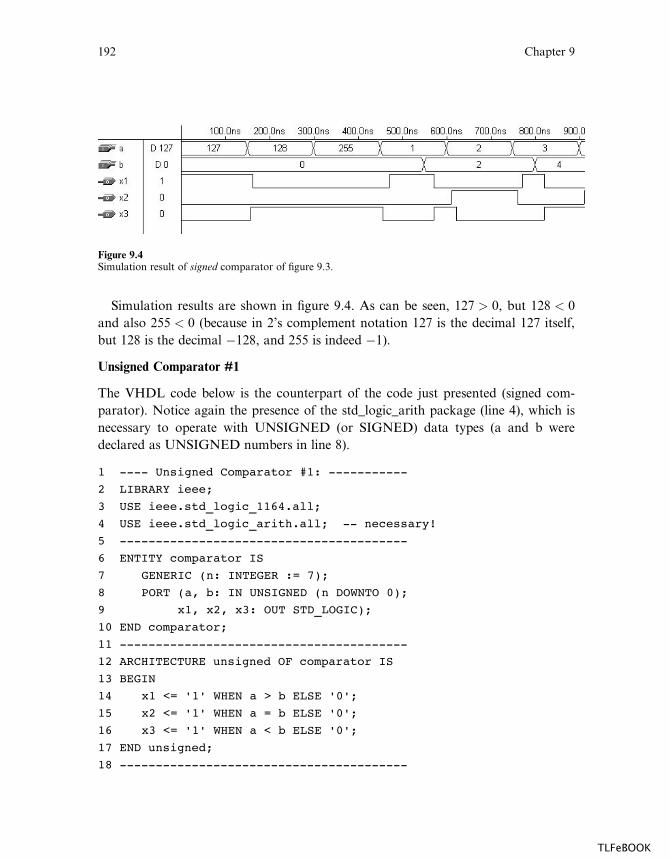
Simulation results are shown in figure 9.4. As can be seen, 127 > 0, but 128 < 0
and also 255 < 0 (because in 2’s complement notation 127 is the decimal 127 itself,
but 128 is the decimal �128, and 255 is indeed �1).
Unsigned Comparator #1
The VHDL code below is the counterpart of the code just presented (signed com-
parator). Notice again the presence of the std_logic_arith package (line 4), which is
necessary to operate with UNSIGNED (or SIGNED) data types (a and b were
declared as UNSIGNED numbers in line 8).
1 ---- Unsigned Comparator #1: -----------
2 LIBRARY ieee;
3 USE ieee.std_logic_1164.all;
4 USE ieee.std_logic_arith.all; -- necessary!
5 ----------------------------------------
6 ENTITY comparator IS
7 GENERIC (n: INTEGER := 7);
8 PORT (a, b: IN UNSIGNED (n DOWNTO 0);
9 x1, x2, x3: OUT STD_LOGIC);
10 END comparator;
11 ----------------------------------------
12 ARCHITECTURE unsigned OF comparator IS
13 BEGIN
14 x1 <= '1' WHEN a > b ELSE '0';
15 x2 <= '1' WHEN a = b ELSE '0';
16 x3 <= '1' WHEN a < b ELSE '0';
17 END unsigned;
18 ----------------------------------------
Figure 9.4Simulation result of signed comparator of figure 9.3.
192 Chapter 9
TLFeBOOK

Unsigned Comparator #2
Unsigned comparators can also be implemented with STD_LOGIC_VECTORS, in
which case there is no need to declare the std_logic_arith package. A solution of this
kind is presented below.
1 ---- Unsigned Comparator #2: -----------
2 LIBRARY ieee;
3 USE ieee.std_logic_1164.all;
4 ----------------------------------------
5 ENTITY comparator IS
6 GENERIC (n: INTEGER := 7);
7 PORT (a, b: IN STD_LOGIC_VECTOR (n DOWNTO 0);
8 x1, x2, x3: OUT STD_LOGIC);
9 END comparator;
10 ----------------------------------------
11 ARCHITECTURE unsigned OF comparator IS
12 BEGIN
13 x1 <= '1' WHEN a > b ELSE '0';
14 x2 <= '1' WHEN a = b ELSE '0';
15 x3 <= '1' WHEN a < b ELSE '0';
16 END unsigned;
17 ----------------------------------------
Simulation results (from either unsigned comparator) are shown in figure 9.5.
Contrary to figure 9.4, now 128 and 255 are indeed bigger than zero.
Figure 9.5Simulation result of unsigned comparator of figure 9.3.
Additional Circuit Designs 193
TLFeBOOK
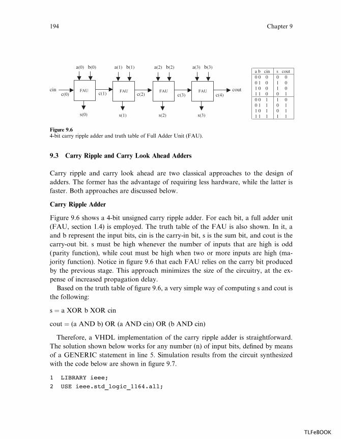
9.3 Carry Ripple and Carry Look Ahead Adders
Carry ripple and carry look ahead are two classical approaches to the design of
adders. The former has the advantage of requiring less hardware, while the latter is
faster. Both approaches are discussed below.
Carry Ripple Adder
Figure 9.6 shows a 4-bit unsigned carry ripple adder. For each bit, a full adder unit
(FAU, section 1.4) is employed. The truth table of the FAU is also shown. In it, a
and b represent the input bits, cin is the carry-in bit, s is the sum bit, and cout is the
carry-out bit. s must be high whenever the number of inputs that are high is odd
(parity function), while cout must be high when two or more inputs are high (ma-
jority function). Notice in figure 9.6 that each FAU relies on the carry bit produced
by the previous stage. This approach minimizes the size of the circuitry, at the ex-
pense of increased propagation delay.
Based on the truth table of figure 9.6, a very simple way of computing s and cout is
the following:
s ¼ a XOR b XOR cin
cout ¼ (a AND b) OR (a AND cin) OR (b AND cin)
Therefore, a VHDL implementation of the carry ripple adder is straightforward.
The solution shown below works for any number (n) of input bits, defined by means
of a GENERIC statement in line 5. Simulation results from the circuit synthesized
with the code below are shown in figure 9.7.
1 LIBRARY ieee;
2 USE ieee.std_logic_1164.all;
a(2) b(2)
coutcin FAU
a(1) b(1) a(3) b(3)
s(2)s(0) s(1) s(3)
c(0) c(4)c(3)FAU
c(2)c(1)
a(0) b(0)
FAU FAU
a b cin s cout0 0 00 1 01 0 01 1 0
0 01 01 00 1
0 0 10 1 11 0 11 1 1
1 00 10 11 1
Figure 9.64-bit carry ripple adder and truth table of Full Adder Unit (FAU).
194 Chapter 9
TLFeBOOK
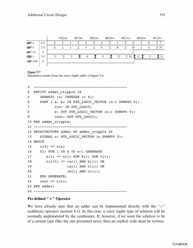
3 ---------------------------------------------
4 ENTITY adder_cripple IS
5 GENERIC (n: INTEGER := 4);
6 PORT ( a, b: IN STD_LOGIC_VECTOR (n-1 DOWNTO 0);
7 cin: IN STD_LOGIC;
8 s: OUT STD_LOGIC_VECTOR (n-1 DOWNTO 0);
9 cout: OUT STD_LOGIC);
10 END adder_cripple;
11 ---------------------------------------------
12 ARCHITECTURE adder OF adder_cripple IS
13 SIGNAL c: STD_LOGIC_VECTOR (n DOWNTO 0);
14 BEGIN
15 c(0) <= cin;
16 G1: FOR i IN 0 TO n-1 GENERATE
17 s(i) <= a(i) XOR b(i) XOR c(i);
18 c(i+1) <= (a(i) AND b(i)) OR
19 (a(i) AND c(i)) OR
20 (b(i) AND c(i));
21 END GENERATE;
22 cout <= c(n);
23 END adder;
24 ---------------------------------------------
Pre-defined ‘‘B’’ Operator
We have already seen that an adder can be implemented directly with the ‘‘þ’’
(addition) operator (section 4.1). In this case, a carry ripple type of solution will be
normally implemented by the synthesizer. If, however, if we want the solution to be
of a certain type (like the one presented next), then an explicit code must be written.
Figure 9.7Simulation results from the carry ripple adder of figure 9.6.
Additional Circuit Designs 195
TLFeBOOK

Carry Look Ahead Adder
A diagram of a 4-bit carry look ahead adder is shown in figure 9.8. Its implementa-
tion is based on the generate and propagate concept, which gives the circuit higher
speed than its carry ripple adder counterpart (at the expense of more silicon area).
Consider two input bits, a and b. The generate (g) and propagate (p) signals are
defined as:
g ¼ a AND b
p ¼ a XOR b
Notice that such signals can be computed in advance, because neither depends on
the carry bit.
If we consider now two input vectors, a ¼ a(n� 1) . . . a(1)a(0) and b ¼ b(n� 1)
. . . b(1)b(0), then the corresponding generate and propagate vectors are g ¼ g(n� 1)
. . . g(1)g(0) and p ¼ p(n� 1) . . . p(1)p(0), where
g( j) ¼ a( j) AND b( j)
p( j) ¼ a( j) XOR b( j)
Let us consider now the carry vector, c ¼ c(n� 1) . . . c(1)c(0). The carry bits can
be computed from g and p:
c(0)C cin
c(1) ¼ c(0)p(0) þ g(0)
cout
PGU
s(0)
p(0) g(0)
a(0) b(0)
PGU
s(1)
p(1) g(1)
a(1) b(1)
PGU
s(2)
p(2) g(2)
a(2) b(2)
PGU
s(3)
p(3) g(3)
a(3) b(3)
cinc(1) c(2) c(3)
c(4)c(0)CLAU
Figure 9.84-bit carry look ahead adder.
196 Chapter 9
TLFeBOOK

c(2) ¼ c(0)p(0)p(1)þ g(0)p(1) þ g(1)
c(3) ¼ c(0)p(0)p(1)p(2)þ g(0)p(1)p(2)þ g(1)p(2) þ g(2), etc.
Notice that, contrary to the carry ripple adder, each carry bit above is computed
independently; that is, none of the expressions above depends on preceding carry
computations, and that is the reason why this circuit is faster. On the other hand, the
hardware complexity grows very fast, limiting this approach to just a few bits (typi-
cally four). Larger carry look ahead adders can be implemented by associating such
4-bit-or-so units.
The implementation of the adder of figure 9.8 is now straightforward. The PGU
(Propagate—Generate Unit) computes p and g (four units are required), plus the
actual sum (s), while the CLAU (Carry Look Ahead Unit) computes the carry bits.
Note: In order to construct bigger carry look ahead adders, the CLAU block of
figure 9.8 must posses Group Propagate (GP) and Group Generate (GG) outputs,
which were omitted in the figure because this implementation is intended for four bits
only.
1 ---------------------------------------------
2 LIBRARY ieee;
3 USE ieee.std_logic_1164.all;
4 ---------------------------------------------
5 ENTITY CLA_Adder IS
6 PORT ( a, b: IN STD_LOGIC_VECTOR (3 DOWNTO 0);
7 cin: IN STD_LOGIC;
8 s: OUT STD_LOGIC_VECTOR (3 DOWNTO 0);
9 cout: OUT STD_LOGIC);
10 END CLA_Adder;
11 ---------------------------------------------
12 ARCHITECTURE CLA_Adder OF CLA_Adder IS
13 SIGNAL c: STD_LOGIC_VECTOR (4 DOWNTO 0);
14 SIGNAL p: STD_LOGIC_VECTOR (3 DOWNTO 0);
15 SIGNAL g: STD_LOGIC_VECTOR (3 DOWNTO 0);
16 BEGIN
17 ---- PGU: ---------------------------------
18 G1: FOR i IN 0 TO 3 GENERATE
19 p(i) <= a(i) XOR b(i);
20 g(i) <= a(i) AND b(i);
21 s(i) <= p(i) XOR c(i);
Additional Circuit Designs 197
TLFeBOOK
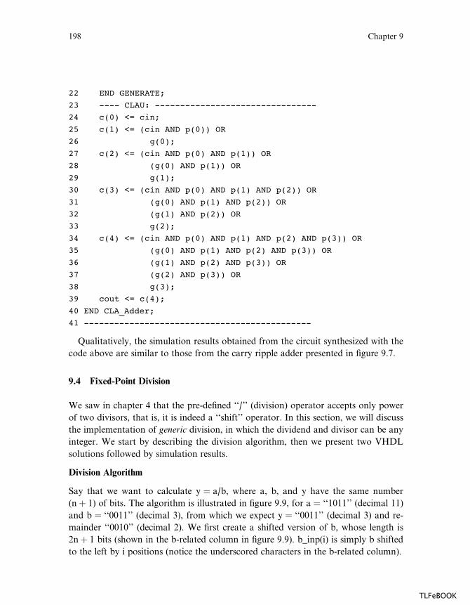
22 END GENERATE;
23 ---- CLAU: --------------------------------
24 c(0) <= cin;
25 c(1) <= (cin AND p(0)) OR
26 g(0);
27 c(2) <= (cin AND p(0) AND p(1)) OR
28 (g(0) AND p(1)) OR
29 g(1);
30 c(3) <= (cin AND p(0) AND p(1) AND p(2)) OR
31 (g(0) AND p(1) AND p(2)) OR
32 (g(1) AND p(2)) OR
33 g(2);
34 c(4) <= (cin AND p(0) AND p(1) AND p(2) AND p(3)) OR
35 (g(0) AND p(1) AND p(2) AND p(3)) OR
36 (g(1) AND p(2) AND p(3)) OR
37 (g(2) AND p(3)) OR
38 g(3);
39 cout <= c(4);
40 END CLA_Adder;
41 ---------------------------------------------
Qualitatively, the simulation results obtained from the circuit synthesized with the
code above are similar to those from the carry ripple adder presented in figure 9.7.
9.4 Fixed-Point Division
We saw in chapter 4 that the pre-defined ‘‘/’’ (division) operator accepts only power
of two divisors, that is, it is indeed a ‘‘shift’’ operator. In this section, we will discuss
the implementation of generic division, in which the dividend and divisor can be any
integer. We start by describing the division algorithm, then we present two VHDL
solutions followed by simulation results.
Division Algorithm
Say that we want to calculate y ¼ a/b, where a, b, and y have the same number
(nþ 1) of bits. The algorithm is illustrated in figure 9.9, for a ¼ ‘‘1011’’ (decimal 11)
and b ¼ ‘‘0011’’ (decimal 3), from which we expect y ¼ ‘‘0011’’ (decimal 3) and re-
mainder ‘‘0010’’ (decimal 2). We first create a shifted version of b, whose length is
2nþ 1 bits (shown in the b-related column in figure 9.9). b_inp(i) is simply b shifted
to the left by i positions (notice the underscored characters in the b-related column).
198 Chapter 9
TLFeBOOK

The computation of the quotient is performed as follows. Starting from the top of
the table, we compare a_inp(i) with b_inp(i). If the former is bigger than or equal
to the latter, than y(i) ¼ ‘1’ and b_inp(i) is subtracted from a_inp(i); otherwise,
y(i) ¼ ‘0’ and we simply proceed to the next line. After nþ 1 iterations, the compu-
tation is completed and the value left in a_inp is the remainder.
Note: It is obvious that, to subtract b_inp from a_inp, the number of bits of a_inp
cannot be less than that of b_inp, so the actual length of a_inp must be increased,
which is attained by simply filling a_inp with n ‘0’s on its left-hand side (‘0’s not
shown in figure 9.9).
Another way of presenting the division algorithm is the following. We multiply b
by 2**n, where nþ 1 is the number of bits. This, of course, corresponds to shifting b
n positions to the left, but without throwing out any of its bits (so the new b-vector
must be n bits longer than the original vector). If a is bigger than the new b, then
y(n) ¼ ‘1’, and b (the new value) must be subtracted from a; otherwise, y(n) ¼ ‘0’.
Now we move to the next iteration. We multiply b (the original value) by 2**(n� 1),
which is equivalent to shifting the original vector n� 1 positions to the left, or shift-
ing the value of b just used in the previous computation back one position to the
right. Then we compare it to a, as we did before, to decide whether y(n� 1) should
be ‘1’ or ‘0’, and so on.
VHDL Dividers
Below are two solutions for the division problem. Both use sequential code: IF is
used in the first, while LOOP plus IF are employed in the second. The first solution is
a step-by-step code, so the division algorithm described above can be clearly
observed. The second is more compact and is also generic (notice that n was defined
Index
(i)
a-related
input (a_inp)
Comparison b-related
input (b_inp)
y (quotient) Operation on 1st column
3
2
1
0
1011
1011
1011
0101
<
<
>
>
0011000
0001100
0000110
0000011
0
0
1
1
none
none
a_inp(i)-b_inp(i)
a_inp(i)-b_inp(i)
0010 (rem)
Figure 9.9Division algorithm.
Additional Circuit Designs 199
TLFeBOOK

by means of a GENERIC statement in line 6). The solutions include also a b ¼ 0
check routine.
Simulation results are shown in figure 9.10.
1 ----- Solution 1: step-by-step -------------------
2 LIBRARY ieee;
3 USE ieee.std_logic_1164.all;
4 --------------------------------------------------
5 ENTITY divider IS
6 PORT ( a, b: IN INTEGER RANGE 0 TO 15;
7 y: OUT STD_LOGIC_VECTOR (3 DOWNTO 0);
8 rest: OUT INTEGER RANGE 0 TO 15;
9 err : OUT STD_LOGIC);
10 END divider;
11 --------------------------------------------------
12 ARCHITECTURE rtl OF divider IS
13 BEGIN
14 PROCESS (a, b)
15 VARIABLE temp1: INTEGER RANGE 0 TO 15;
16 VARIABLE temp2: INTEGER RANGE 0 TO 15;
17 BEGIN
18 ----- Error and initialization: -------
19 temp1 := a;
20 temp2 := b;
21 IF (b=0) THEN err <= '1';
22 ELSE err <= '0';
23 END IF;
24 ----- y(3): ---------------------------
Figure 9.10Simulation results of divider (for 4-bit operands).
200 Chapter 9
TLFeBOOK

25 IF (temp1 >= temp2 * 8) THEN
26 y(3) <= '1';
27 temp1 := temp1 - temp2*8;
28 ELSE y(3) <= '0';
29 END IF;
30 ----- y(2): ---------------------------
31 IF (temp1 >= temp2 * 4) THEN
32 y(2) <= '1';
33 temp1 := temp1 - temp2 * 4;
34 ELSE y(2) <= '0';
35 END IF;
36 ----- y(1): ---------------------------
37 IF (temp1 >= temp2 * 2) THEN
38 y(1) <= '1';
39 temp1 := temp1 - temp2 * 2;
40 ELSE y(1) <= '0';
41 END IF;
42 ----- y(0): ---------------------------
43 IF (temp1 >= temp2) THEN
44 y(0) <= '1';
45 temp1 := temp1 - temp2;
46 ELSE y(0) <= '0';
47 END IF;
48 ----- Remainder: ----------------------
49 rest <= temp1;
50 END PROCESS;
51 END rtl;
52 --------------------------------------------------
1 ------ Solution 2: compact and generic -----------
2 LIBRARY ieee;
3 USE ieee.std_logic_1164.all;
4 --------------------------------------------------
5 ENTITY divider IS
6 GENERIC(n: INTEGER := 3);
7 PORT ( a, b: IN INTEGER RANGE 0 TO 15;
8 y: OUT STD_LOGIC_VECTOR (3 DOWNTO 0);
9 rest: OUT INTEGER RANGE 0 TO 15;
Additional Circuit Designs 201
TLFeBOOK
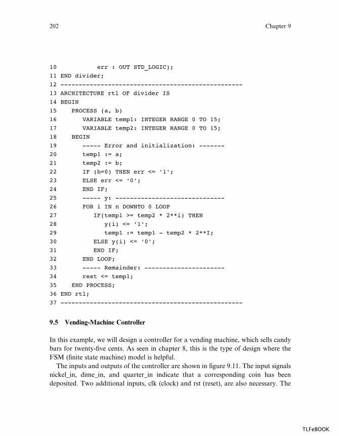
10 err : OUT STD_LOGIC);
11 END divider;
12 --------------------------------------------------
13 ARCHITECTURE rtl OF divider IS
14 BEGIN
15 PROCESS (a, b)
16 VARIABLE temp1: INTEGER RANGE 0 TO 15;
17 VARIABLE temp2: INTEGER RANGE 0 TO 15;
18 BEGIN
19 ----- Error and initialization: -------
20 temp1 := a;
21 temp2 := b;
22 IF (b=0) THEN err <= '1';
23 ELSE err <= '0';
24 END IF;
25 ----- y: ------------------------------
26 FOR i IN n DOWNTO 0 LOOP
27 IF(temp1 >= temp2 * 2**i) THEN
28 y(i) <= '1';
29 temp1 := temp1 - temp2 * 2**I;
30 ELSE y(i) <= '0';
31 END IF;
32 END LOOP;
33 ----- Remainder: ----------------------
34 rest <= temp1;
35 END PROCESS;
36 END rtl;
37 --------------------------------------------------
9.5 Vending-Machine Controller
In this example, we will design a controller for a vending machine, which sells candy
bars for twenty-five cents. As seen in chapter 8, this is the type of design where the
FSM (finite state machine) model is helpful.
The inputs and outputs of the controller are shown in figure 9.11. The input signals
nickel_in, dime_in, and quarter_in indicate that a corresponding coin has been
deposited. Two additional inputs, clk (clock) and rst (reset), are also necessary. The
202 Chapter 9
TLFeBOOK

co
do+co
no+c
di
di
di
ni
ni ni ni
niqiqiqi
qi
di
di
0
10
45403530
25
20155
qi
do
no
nickel_in
dime_in
quarter_in
clk rst
Vending-machinecontroller
candy_out
nickel_out
dime_out
Figure 9.11Vending-machine controller (top-level and states diagrams). The signals are. ni ¼ nickel_in, di ¼ dime_in,qi ¼ quarter_in, no ¼ nickel_out, do ¼ dime_out, and co ¼ candy_out.
Additional Circuit Designs 203
TLFeBOOK
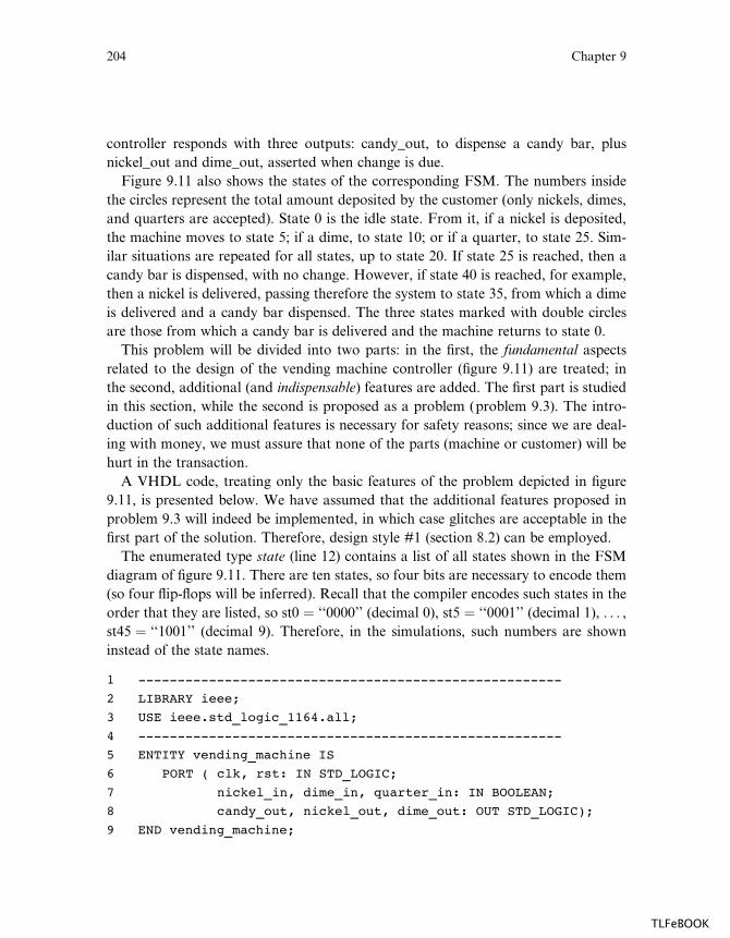
controller responds with three outputs: candy_out, to dispense a candy bar, plus
nickel_out and dime_out, asserted when change is due.
Figure 9.11 also shows the states of the corresponding FSM. The numbers inside
the circles represent the total amount deposited by the customer (only nickels, dimes,
and quarters are accepted). State 0 is the idle state. From it, if a nickel is deposited,
the machine moves to state 5; if a dime, to state 10; or if a quarter, to state 25. Sim-
ilar situations are repeated for all states, up to state 20. If state 25 is reached, then a
candy bar is dispensed, with no change. However, if state 40 is reached, for example,
then a nickel is delivered, passing therefore the system to state 35, from which a dime
is delivered and a candy bar dispensed. The three states marked with double circles
are those from which a candy bar is delivered and the machine returns to state 0.
This problem will be divided into two parts: in the first, the fundamental aspects
related to the design of the vending machine controller (figure 9.11) are treated; in
the second, additional (and indispensable) features are added. The first part is studied
in this section, while the second is proposed as a problem (problem 9.3). The intro-
duction of such additional features is necessary for safety reasons; since we are deal-
ing with money, we must assure that none of the parts (machine or customer) will be
hurt in the transaction.
A VHDL code, treating only the basic features of the problem depicted in figure
9.11, is presented below. We have assumed that the additional features proposed in
problem 9.3 will indeed be implemented, in which case glitches are acceptable in the
first part of the solution. Therefore, design style #1 (section 8.2) can be employed.
The enumerated type state (line 12) contains a list of all states shown in the FSM
diagram of figure 9.11. There are ten states, so four bits are necessary to encode them
(so four flip-flops will be inferred). Recall that the compiler encodes such states in the
order that they are listed, so st0 ¼ ‘‘0000’’ (decimal 0), st5 ¼ ‘‘0001’’ (decimal 1), . . . ,
st45 ¼ ‘‘1001’’ (decimal 9). Therefore, in the simulations, such numbers are shown
instead of the state names.
1 ------------------------------------------------------
2 LIBRARY ieee;
3 USE ieee.std_logic_1164.all;
4 ------------------------------------------------------
5 ENTITY vending_machine IS
6 PORT ( clk, rst: IN STD_LOGIC;
7 nickel_in, dime_in, quarter_in: IN BOOLEAN;
8 candy_out, nickel_out, dime_out: OUT STD_LOGIC);
9 END vending_machine;
204 Chapter 9
TLFeBOOK
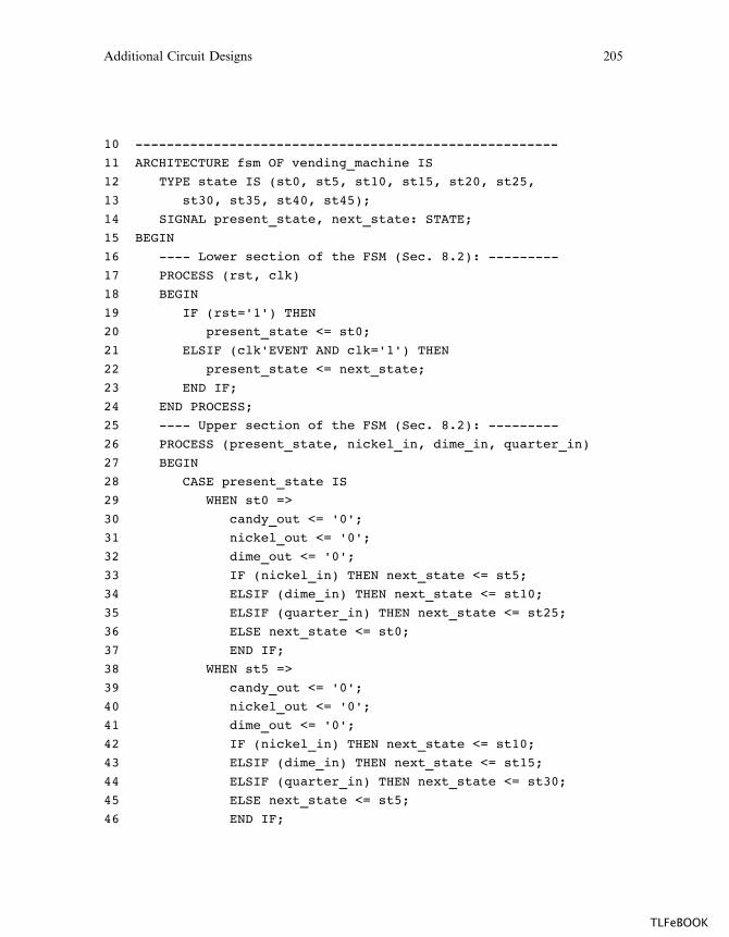
10 ------------------------------------------------------
11 ARCHITECTURE fsm OF vending_machine IS
12 TYPE state IS (st0, st5, st10, st15, st20, st25,
13 st30, st35, st40, st45);
14 SIGNAL present_state, next_state: STATE;
15 BEGIN
16 ---- Lower section of the FSM (Sec. 8.2): ---------
17 PROCESS (rst, clk)
18 BEGIN
19 IF (rst='1') THEN
20 present_state <= st0;
21 ELSIF (clk'EVENT AND clk='1') THEN
22 present_state <= next_state;
23 END IF;
24 END PROCESS;
25 ---- Upper section of the FSM (Sec. 8.2): ---------
26 PROCESS (present_state, nickel_in, dime_in, quarter_in)
27 BEGIN
28 CASE present_state IS
29 WHEN st0 =>
30 candy_out <= '0';
31 nickel_out <= '0';
32 dime_out <= '0';
33 IF (nickel_in) THEN next_state <= st5;
34 ELSIF (dime_in) THEN next_state <= st10;
35 ELSIF (quarter_in) THEN next_state <= st25;
36 ELSE next_state <= st0;
37 END IF;
38 WHEN st5 =>
39 candy_out <= '0';
40 nickel_out <= '0';
41 dime_out <= '0';
42 IF (nickel_in) THEN next_state <= st10;
43 ELSIF (dime_in) THEN next_state <= st15;
44 ELSIF (quarter_in) THEN next_state <= st30;
45 ELSE next_state <= st5;
46 END IF;
Additional Circuit Designs 205
TLFeBOOK
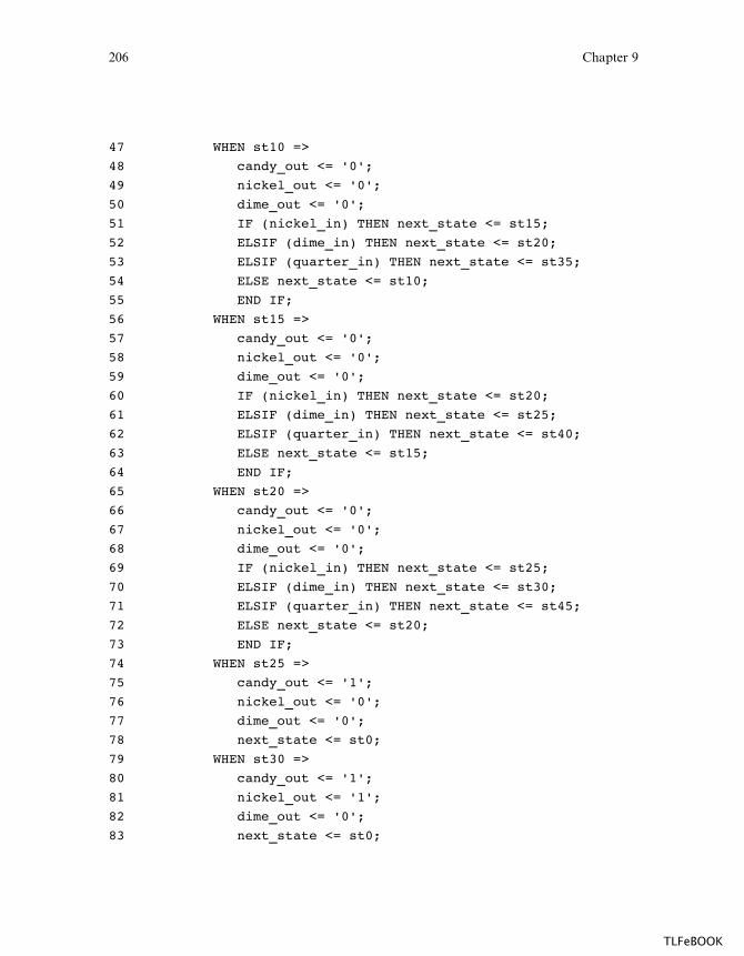
47 WHEN st10 =>
48 candy_out <= '0';
49 nickel_out <= '0';
50 dime_out <= '0';
51 IF (nickel_in) THEN next_state <= st15;
52 ELSIF (dime_in) THEN next_state <= st20;
53 ELSIF (quarter_in) THEN next_state <= st35;
54 ELSE next_state <= st10;
55 END IF;
56 WHEN st15 =>
57 candy_out <= '0';
58 nickel_out <= '0';
59 dime_out <= '0';
60 IF (nickel_in) THEN next_state <= st20;
61 ELSIF (dime_in) THEN next_state <= st25;
62 ELSIF (quarter_in) THEN next_state <= st40;
63 ELSE next_state <= st15;
64 END IF;
65 WHEN st20 =>
66 candy_out <= '0';
67 nickel_out <= '0';
68 dime_out <= '0';
69 IF (nickel_in) THEN next_state <= st25;
70 ELSIF (dime_in) THEN next_state <= st30;
71 ELSIF (quarter_in) THEN next_state <= st45;
72 ELSE next_state <= st20;
73 END IF;
74 WHEN st25 =>
75 candy_out <= '1';
76 nickel_out <= '0';
77 dime_out <= '0';
78 next_state <= st0;
79 WHEN st30 =>
80 candy_out <= '1';
81 nickel_out <= '1';
82 dime_out <= '0';
83 next_state <= st0;
206 Chapter 9
TLFeBOOK
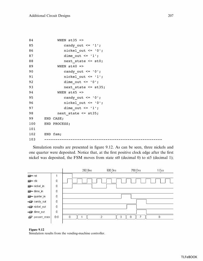
84 WHEN st35 =>
85 candy_out <= '1';
86 nickel_out <= '0';
87 dime_out <= '1';
88 next_state <= st0;
89 WHEN st40 =>
90 candy_out <= '0';
91 nickel_out <= '1';
92 dime_out <= '0';
93 next_state <= st35;
94 WHEN st45 =>
95 candy_out <= '0';
96 nickel_out <= '0';
97 dime_out <= '1';
98 next_state <= st35;
99 END CASE;
100 END PROCESS;
101
102 END fsm;
103 ------------------------------------------------------
Simulation results are presented in figure 9.12. As can be seen, three nickels and
one quarter were deposited. Notice that, at the first positive clock edge after the first
nickel was deposited, the FSM moves from state st0 (decimal 0) to st5 (decimal 1);
Figure 9.12Simulation results from the vending-machine controller.
Additional Circuit Designs 207
TLFeBOOK

after de second nickel, to state st10 (decimal 2); after de third, to state st15 (decimal
3); and, after de quarter has been deposited, to state st40 (decimal 8). After that, a
nickel is returned to the customer (nickel_out ¼ ‘1’), causing the FSM to move to
state st35 (decimal 7), at which a dime is delivered (dime_out ¼ ‘1’) and a candy bar
is dispensed (candy_out ¼ ‘1’). The system returns then to its idle state (st0).
As mentioned above, additional features (like handshake) are necessary to increase
the security of the transactions. Please refer to problem 9.3 for a continuation of this
design.
9.6 Serial Data Receiver
The diagram of a serial data receiver is shown in figure 9.13. It contains a serial data
input, din, and a parallel data output, data(6:0). A clock signal is also needed at the
input. Two supervision signals are generated by the circuit: err (error) and data_valid.
The input train consists of ten bits. The first bit is a start bit, which, when high,
must cause the circuit to start receiving data. The next seven are the actual data bits.
The ninth bit is a parity bit, whose status must be ‘0’ if the number of ones in data is
even, or ‘1’ otherwise. Finally, the tenth is a stop bit, which must be high if the
transmission is correct. An error is detected when either the parity does not check or
the stop bit is not a ‘1’. When reception is concluded and if no error has been
detected, then the data stored in the internal registers (reg) is transferred to data(6:0)
and the data_valid output is asserted.
A VHDL code for this circuit is presented below. A few variables were used:
count, to determine the number of bits received; reg, which stores the data; and temp,
to compute the error. Notice in line 37 that reg(0) ¼ din was used instead of
reg(0) ¼ ‘0’, because we want the time slot immediately after the stop bit to be con-
sidered as possibly containing a start bit for the next input train.
err
data_valid
data (0) (1) (2) (3) (4) (5) (6)
data
din
clk
start parity stop
reg
Figure 9.13Serial data receiver.
208 Chapter 9
TLFeBOOK
1 ---------------------------------------------
2 LIBRARY ieee;
3 USE ieee.std_logic_1164.all;
4 ---------------------------------------------
5 ENTITY receiver IS
6 PORT ( din, clk, rst: IN BIT;
7 data: OUT BIT_VECTOR (6 DOWNTO 0);
8 err, data_valid: OUT BIT);
9 END receiver;
10 ---------------------------------------------
11 ARCHITECTURE rtl OF receiver IS
12 BEGIN
13 PROCESS (rst, clk)
14 VARIABLE count: INTEGER RANGE 0 TO 10;
15 VARIABLE reg: BIT_VECTOR (10 DOWNTO 0);
16 VARIABLE temp : BIT;
17 BEGIN
18 IF (rst='1') THEN
19 count:=0;
20 reg := (reg'RANGE => '0');
21 temp := '0';
22 err <= '0';
23 data_valid <= '0';
24 ELSIF (clk'EVENT AND clk='1') THEN
25 IF (reg(0)='0' AND din='1') THEN
26 reg(0) := '1';
27 ELSIF (reg(0)='1') THEN
28 count := count + 1;
29 IF (count < 10) THEN
30 reg(count) := din;
31 ELSIF (count = 10) THEN
32 temp := (reg(1) XOR reg(2) XOR reg(3) XOR
33 reg(4) XOR reg(5) XOR reg(6) XOR
34 reg(7) XOR reg(8)) OR NOT reg(9);
35 err <= temp;
36 count := 0;
37 reg(0) := din;
38 IF (temp = '0') THEN
Additional Circuit Designs 209
TLFeBOOK
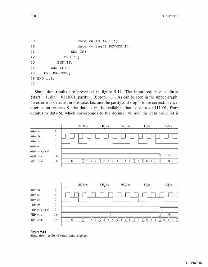
39 data_valid <= '1';
40 data <= reg(7 DOWNTO 1);
41 END IF;
42 END IF;
43 END IF;
44 END IF;
45 END PROCESS;
46 END rtl;
47 -------------------------------------------------
Simulation results are presented in figure 9.14. The input sequence is din ¼{start ¼ 1, din ¼ 0111001, parity ¼ 0, stop ¼ 1}. As can be seen in the upper graph,
no error was detected in this case, because the parity and stop bits are correct. Hence,
after count reaches 9, the data is made available, that is, data ¼ 0111001, from
data(0) to data(6), which corresponds to the decimal 78, and the data_valid bit is
Figure 9.14Simulation results of serial data receivers.
210 Chapter 9
TLFeBOOK

asserted. Notice that the output remains so indefinitely, unless a new input train is
received.
The only di¤erence in the lower graph is that a start bit appears immediately after
the stop bit. As can be seen, the count variable starts then to count and the whole
process is repeated.
9.7 Parallel-to-Serial Converter
A parallel-to-serial converter is a typical application of shift registers. It consists of
sending out a block of data serially. The need for such converters arises, for example,
in ASIC chips when there are not enough pins available to output all data bits
simultaneously.
A diagram of a parallel-to-serial converter is presented in figure 9.15. d(7:0) is the
data vector to be sent out, while dout is the actual output. There are also two other
inputs: clk and load. When load is asserted, d is synchronously stored in the shift
register reg. While load stays high, the MSB, d(7), remains available at the output.
Once load is returned to ‘0’, the subsequent bits are presented at the output at each
positive edge of clk. After all eight bits have been sent out, the output remains low
until the next transmission.
1 -------------------------------------------------
2 LIBRARY ieee;
3 USE ieee.std_logic_1164.all;
4 -------------------------------------------------
5 ENTITY serial_converter IS
6 PORT ( d: IN STD_LOGIC_VECTOR (7 DOWNTO 0);
7 clk, load: IN STD_LOGIC;
8 dout: OUT STD_LOGIC);
9 END serial_converter;
10 -------------------------------------------------
d(0) d(1) d(2) d(3) d(4) d(5) d(6) d(7)
dout clkload
reg
Figure 9.15Parallel-to-serial converter.
Additional Circuit Designs 211
TLFeBOOK
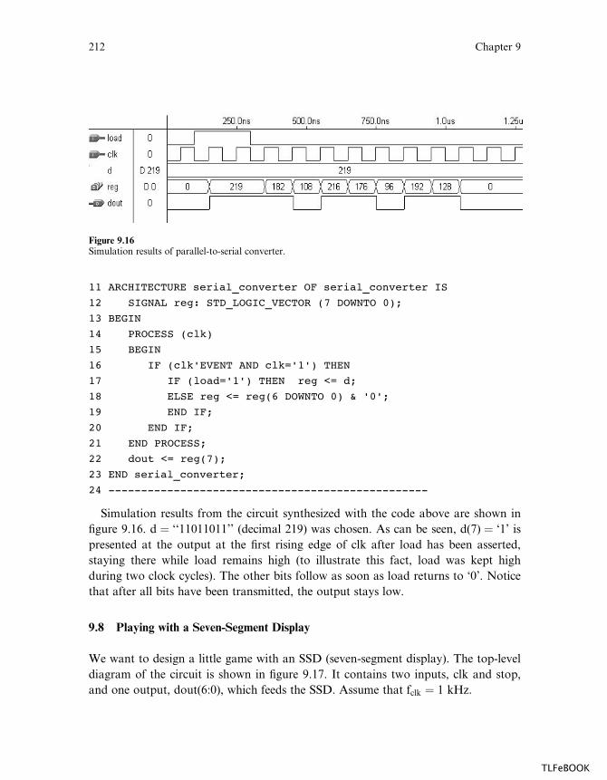
11 ARCHITECTURE serial_converter OF serial_converter IS
12 SIGNAL reg: STD_LOGIC_VECTOR (7 DOWNTO 0);
13 BEGIN
14 PROCESS (clk)
15 BEGIN
16 IF (clk'EVENT AND clk='1') THEN
17 IF (load='1') THEN reg <= d;
18 ELSE reg <= reg(6 DOWNTO 0) & '0';
19 END IF;
20 END IF;
21 END PROCESS;
22 dout <= reg(7);
23 END serial_converter;
24 -------------------------------------------------
Simulation results from the circuit synthesized with the code above are shown in
figure 9.16. d ¼ ‘‘11011011’’ (decimal 219) was chosen. As can be seen, d(7) ¼ ‘1’ is
presented at the output at the first rising edge of clk after load has been asserted,
staying there while load remains high (to illustrate this fact, load was kept high
during two clock cycles). The other bits follow as soon as load returns to ‘0’. Notice
that after all bits have been transmitted, the output stays low.
9.8 Playing with a Seven-Segment Display
We want to design a little game with an SSD (seven-segment display). The top-level
diagram of the circuit is shown in figure 9.17. It contains two inputs, clk and stop,
and one output, dout(6:0), which feeds the SSD. Assume that fclk ¼ 1 kHz.
Figure 9.16Simulation results of parallel-to-serial converter.
212 Chapter 9
TLFeBOOK
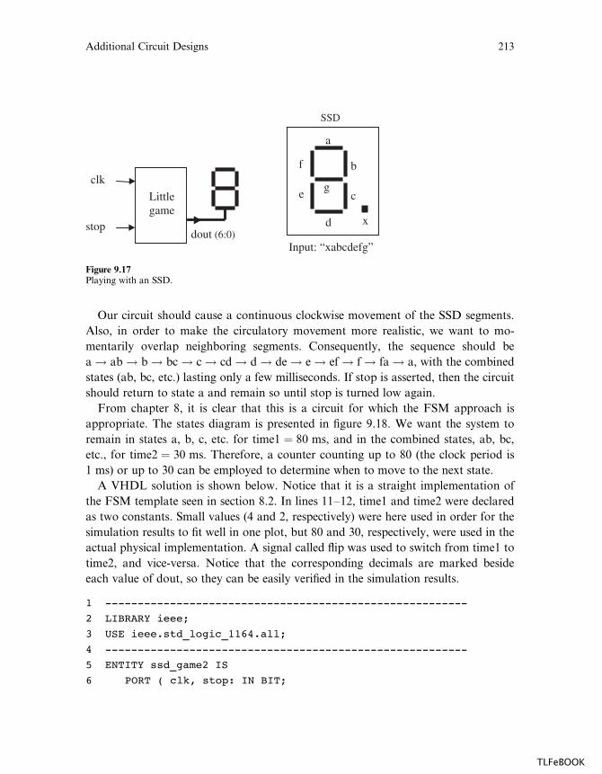
Our circuit should cause a continuous clockwise movement of the SSD segments.
Also, in order to make the circulatory movement more realistic, we want to mo-
mentarily overlap neighboring segments. Consequently, the sequence should be
a ! ab ! b ! bc ! c ! cd ! d ! de ! e ! ef ! f ! fa ! a, with the combined
states (ab, bc, etc.) lasting only a few milliseconds. If stop is asserted, then the circuit
should return to state a and remain so until stop is turned low again.
From chapter 8, it is clear that this is a circuit for which the FSM approach is
appropriate. The states diagram is presented in figure 9.18. We want the system to
remain in states a, b, c, etc. for time1 ¼ 80 ms, and in the combined states, ab, bc,
etc., for time2 ¼ 30 ms. Therefore, a counter counting up to 80 (the clock period is
1 ms) or up to 30 can be employed to determine when to move to the next state.
A VHDL solution is shown below. Notice that it is a straight implementation of
the FSM template seen in section 8.2. In lines 11–12, time1 and time2 were declared
as two constants. Small values (4 and 2, respectively) were here used in order for the
simulation results to fit well in one plot, but 80 and 30, respectively, were used in the
actual physical implementation. A signal called flip was used to switch from time1 to
time2, and vice-versa. Notice that the corresponding decimals are marked beside
each value of dout, so they can be easily verified in the simulation results.
1 --------------------------------------------------------
2 LIBRARY ieee;
3 USE ieee.std_logic_1164.all;
4 --------------------------------------------------------
5 ENTITY ssd_game2 IS
6 PORT ( clk, stop: IN BIT;
dout (6:0)
clk
stop
Littlegame
SSD
e
f
a
b
c
d
g
x
Input: “xabcdefg”
Figure 9.17Playing with an SSD.
Additional Circuit Designs 213
TLFeBOOK
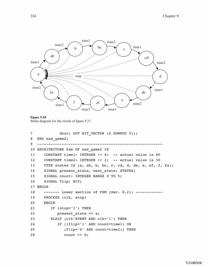
7 dout: OUT BIT_VECTOR (6 DOWNTO 0));
8 END ssd_game2;
9 --------------------------------------------------------
10 ARCHITECTURE fsm OF ssd_game2 IS
11 CONSTANT time1: INTEGER := 4; -- actual value is 80
12 CONSTANT time2: INTEGER := 2; -- actual value is 30
13 TYPE states IS (a, ab, b, bc, c, cd, d, de, e, ef, f, fa);
14 SIGNAL present_state, next_state: STATES;
15 SIGNAL count: INTEGER RANGE 0 TO 5;
16 SIGNAL flip: BIT;
17 BEGIN
18 ------- Lower section of FSM (Sec. 8.2): ------------
19 PROCESS (clk, stop)
20 BEGIN
21 IF (stop='1') THEN
22 present_state <= a;
23 ELSIF (clk'EVENT AND clk='1') THEN
24 IF ((flip='1' AND count=time1) OR
25 (flip='0' AND count=time2)) THEN
26 count <= 0;
time2
a
time1
d
ab cd
b cbc
fa de
fe
ef
time2time1
time1
time1
time1time1
time2
time2
time2
time2
stop
Figure 9.18States diagram for the circuit of figure 9.17.
214 Chapter 9
TLFeBOOK
27 present_state <= next_state;
28 ELSE count <= count + 1;
29 END IF;
30 END IF;
31 END PROCESS;
32 ------- Upper section of FSM (Sec. 8.2): ------------
33 PROCESS (present_state)
34 BEGIN
35 CASE present_state IS
36 WHEN a =>
37 dout <= "1000000"; -- Decimal 64
38 flip<='1';
39 next_state <= ab;
40 WHEN ab =>
41 dout <= "1100000"; -- Decimal 96
42 flip<='0';
43 next_state <= b;
44 WHEN b =>
45 dout <= "0100000"; -- Decimal 32
46 flip<='1';
47 next_state <= bc;
48 WHEN bc =>
49 dout <= "0110000"; -- Decimal 48
50 flip<='0';
51 next_state <= c;
52 WHEN c =>
53 dout <= "0010000"; -- Decimal 16
54 flip<='1';
55 next_state <= cd;
56 WHEN cd =>
57 dout <= "0011000"; -- Decimal 24
58 flip<='0';
59 next_state <= d;
60 WHEN d =>
61 dout <= "0001000"; -- Decimal 8
62 flip<='1';
63 next_state <= de;
Additional Circuit Designs 215
TLFeBOOK

64 WHEN de =>
65 dout <= "0001100"; -- Decimal 12
66 flip<='0';
67 next_state <= e;
68 WHEN e =>
69 dout <= "0000100"; -- Decimal 4
70 flip<='1';
71 next_state <= ef;
72 WHEN ef =>
73 dout <= "0000110"; -- Decimal 6
74 flip<='0';
75 next_state <= f;
76 WHEN f =>
77 dout <= "0000010"; -- Decimal 2
78 flip<='1';
79 next_state <= fa;
80 WHEN fa =>
81 dout <= "1000010"; -- Decimal 66
82 flip<='0';
83 next_state <= a;
84 END CASE;
85 END PROCESS;
86 END fsm;
87 --------------------------------------------------------
Simulation results are presented in figure 9.19. As can be seen, the system stays in
the single states, a, b, etc., for four clock cycles (time1 ¼ 4 here) and in the combined
states, ab, bc, etc., for two clock cycles (time2 ¼ 2). Observe also that the decimals
detected by the simulator match the decimals listed in the VHDL code.
Figure 9.19Simulation results of little SSD game of figure 9.17.
216 Chapter 9
TLFeBOOK
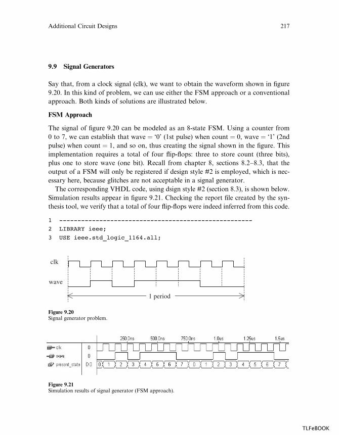
9.9 Signal Generators
Say that, from a clock signal (clk), we want to obtain the waveform shown in figure
9.20. In this kind of problem, we can use either the FSM approach or a conventional
approach. Both kinds of solutions are illustrated below.
FSM Approach
The signal of figure 9.20 can be modeled as an 8-state FSM. Using a counter from
0 to 7, we can establish that wave ¼ ‘0’ (1st pulse) when count ¼ 0, wave ¼ ‘1’ (2nd
pulse) when count ¼ 1, and so on, thus creating the signal shown in the figure. This
implementation requires a total of four flip-flops: three to store count (three bits),
plus one to store wave (one bit). Recall from chapter 8, sections 8.2–8.3, that the
output of a FSM will only be registered if design style #2 is employed, which is nec-
essary here, because glitches are not acceptable in a signal generator.
The corresponding VHDL code, using dsign style #2 (section 8.3), is shown below.
Simulation results appear in figure 9.21. Checking the report file created by the syn-
thesis tool, we verify that a total of four flip-flops were indeed inferred from this code.
1 -----------------------------------------------------
2 LIBRARY ieee;
3 USE ieee.std_logic_1164.all;
clk
wave
1 period
Figure 9.20Signal generator problem.
Figure 9.21Simulation results of signal generator (FSM approach).
Additional Circuit Designs 217
TLFeBOOK
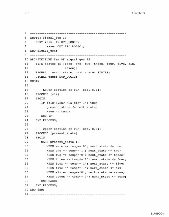
4 -----------------------------------------------------
5 ENTITY signal_gen IS
6 PORT (clk: IN STD_LOGIC;
7 wave: OUT STD_LOGIC);
8 END signal_gen;
9 -----------------------------------------------------
10 ARCHITECTURE fsm OF signal_gen IS
11 TYPE states IS (zero, one, two, three, four, five, six,
12 seven);
13 SIGNAL present_state, next_state: STATES;
14 SIGNAL temp: STD_LOGIC;
15 BEGIN
16
17 --- Lower section of FSM (Sec. 8.3): ---
18 PROCESS (clk)
19 BEGIN
20 IF (clk'EVENT AND clk='1') THEN
21 present_state <= next_state;
22 wave <= temp;
23 END IF;
24 END PROCESS;
25
26 --- Upper section of FSM (Sec. 8.3): ---
27 PROCESS (present_state)
28 BEGIN
29 CASE present_state IS
30 WHEN zero => temp<='0'; next_state <= one;
31 WHEN one => temp<='1'; next_state <= two;
32 WHEN two => temp<='0'; next_state <= three;
33 WHEN three => temp<='1'; next_state <= four;
34 WHEN four => temp<='1'; next_state <= five;
35 WHEN five => temp<='1'; next_state <= six;
36 WHEN six => temp<='0'; next_state <= seven;
37 WHEN seven => temp<='0'; next_state <= zero;
38 END CASE;
39 END PROCESS;
40 END fsm;
41 -----------------------------------------------------
218 Chapter 9
TLFeBOOK

Conventional Approach
A conventional design, with the IF statement, is shown next. Notice that count and
wave are both assigned at the transition of another signal (clk). Therefore, according
to what you saw in section 7.5, both will be stored (that is, four flip-flops will be in-
ferred, three for count and one for wave). Simulation results are shown in figure 9.22.
1 ---------------------------------------
2 LIBRARY ieee;
3 USE ieee.std_logic_1164.all;
4 ---------------------------------------
5 ENTITY signal_gen1 IS
6 PORT (clk: IN BIT;
7 wave: OUT BIT);
8 END signal_gen1;
9 ---------------------------------------
10 ARCHITECTURE arch1 OF signal_gen1 IS
11 BEGIN
12 PROCESS
13 VARIABLE count: INTEGER RANGE 0 TO 7;
14 BEGIN
15 WAIT UNTIL (clk'EVENT AND clk='1');
16 CASE count IS
17 WHEN 0 => wave <= '0';
18 WHEN 1 => wave <= '1';
19 WHEN 2 => wave <= '0';
20 WHEN 3 => wave <= '1';
21 WHEN 4 => wave <= '1';
22 WHEN 5 => wave <= '1';
23 WHEN 6 => wave <= '0';
Figure 9.22Simulation results of signal generator (conventional approach).
Additional Circuit Designs 219
TLFeBOOK
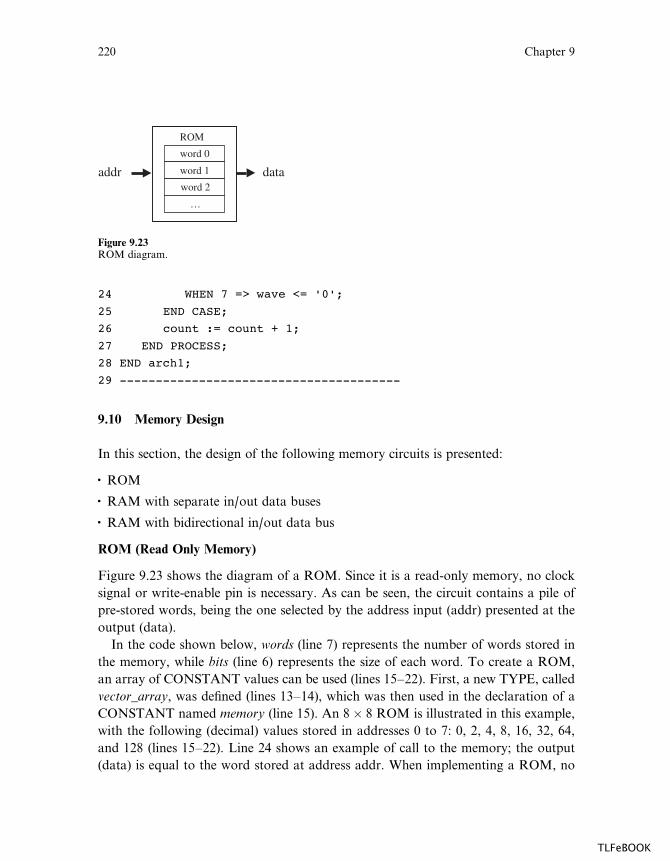
24 WHEN 7 => wave <= '0';
25 END CASE;
26 count := count + 1;
27 END PROCESS;
28 END arch1;
29 ---------------------------------------
9.10 Memory Design
In this section, the design of the following memory circuits is presented:
� ROM
� RAM with separate in/out data buses
� RAM with bidirectional in/out data bus
ROM (Read Only Memory)
Figure 9.23 shows the diagram of a ROM. Since it is a read-only memory, no clock
signal or write-enable pin is necessary. As can be seen, the circuit contains a pile of
pre-stored words, being the one selected by the address input (addr) presented at the
output (data).
In the code shown below, words (line 7) represents the number of words stored in
the memory, while bits (line 6) represents the size of each word. To create a ROM,
an array of CONSTANT values can be used (lines 15–22). First, a new TYPE, called
vector_array, was defined (lines 13–14), which was then used in the declaration of a
CONSTANT named memory (line 15). An 8� 8 ROM is illustrated in this example,
with the following (decimal) values stored in addresses 0 to 7: 0, 2, 4, 8, 16, 32, 64,
and 128 (lines 15–22). Line 24 shows an example of call to the memory; the output
(data) is equal to the word stored at address addr. When implementing a ROM, no
data
ROM
word 0
word 1
word 2
…
addr
Figure 9.23ROM diagram.
220 Chapter 9
TLFeBOOK

registers are inferred, because no signal assignment occurs at the transition of an-
other signal. Logical gates, forming an LUT (lookup table), are used instead.
1 ---------------------------------------------------
2 LIBRARY ieee;
3 USE ieee.std_logic_1164.all;
4 ---------------------------------------------------
5 ENTITY rom IS
6 GENERIC ( bits: INTEGER := 8; -- # of bits per word
7 words: INTEGER := 8); -- # of words in the memory
8 PORT ( addr: IN INTEGER RANGE 0 TO words-1;
9 data: OUT STD_LOGIC_VECTOR (bits-1 DOWNTO 0));
10 END rom;
11 ---------------------------------------------------
12 ARCHITECTURE rom OF rom IS
13 TYPE vector_array IS ARRAY (0 TO words-1) OF
14 STD_LOGIC_VECTOR (bits-1 DOWNTO 0);
15 CONSTANT memory: vector_array := ( "00000000",
16 "00000010",
17 "00000100",
18 "00001000",
19 "00010000",
20 "00100000",
21 "01000000",
22 "10000000");
23 BEGIN
24 data <= memory(addr);
25 END rom;
26 ---------------------------------------------------
Simulation results are shown in figure 9.24. As can be seen, the address changes
from 0 to 7, then restarts from 0, with the outputs matching the values listed in the
code above.
RAM with Separate Input and Output Data Buses
A RAM (Random Access Memory), with separate input and output data buses, is
illustrated in figure 9.25. Indeed, this circuit was already discussed in example 6.11,
but was repeated here to ease the comparison with the other memory circuits pre-
sented in this section.
Additional Circuit Designs 221
TLFeBOOK
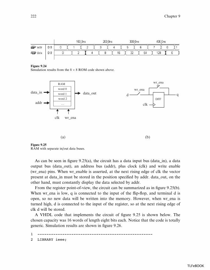
As can be seen in figure 9.25(a), the circuit has a data input bus (data_in), a data
output bus (data_out), an address bus (addr), plus clock (clk) and write enable
(wr_ena) pins. When wr_enable is asserted, at the next rising edge of clk the vector
present at data_in must be stored in the position specified by addr. data_out, on the
other hand, must constantly display the data selected by addr.
From the register point-of-view, the circuit can be summarized as in figure 9.25(b).
When wr_ena is low, q is connected to the input of the flip-flop, and terminal d is
open, so no new data will be written into the memory. However, when wr_ena is
turned high, d is connected to the input of the register, so at the next rising edge of
clk d will be stored.
A VHDL code that implements the circuit of figure 9.25 is shown below. The
chosen capacity was 16 words of length eight bits each. Notice that the code is totally
generic. Simulation results are shown in figure 9.26.
1 ---------------------------------------------------
2 LIBRARY ieee;
Figure 9.24Simulation results from the 8� 8 ROM code shown above.
(a) (b)
clk
DFFd q
wr_ena
wr_ena
data_outdata_in
RAM
word 0
word 1
word 2
…
clk
addr
wr_ena
Figure 9.25RAM with separate in/out data buses.
222 Chapter 9
TLFeBOOK
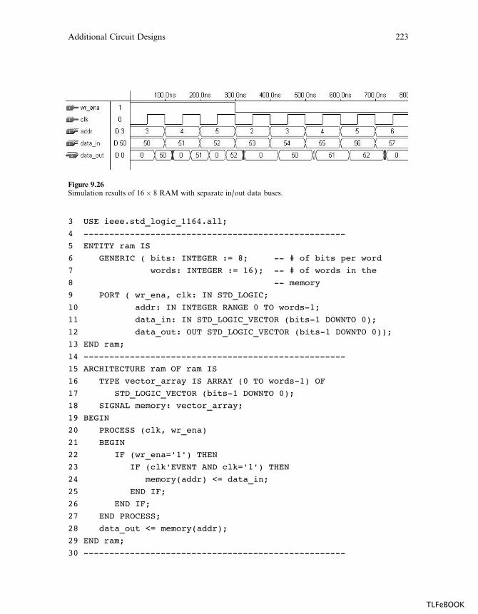
3 USE ieee.std_logic_1164.all;
4 ---------------------------------------------------
5 ENTITY ram IS
6 GENERIC ( bits: INTEGER := 8; -- # of bits per word
7 words: INTEGER := 16); -- # of words in the
8 -- memory
9 PORT ( wr_ena, clk: IN STD_LOGIC;
10 addr: IN INTEGER RANGE 0 TO words-1;
11 data_in: IN STD_LOGIC_VECTOR (bits-1 DOWNTO 0);
12 data_out: OUT STD_LOGIC_VECTOR (bits-1 DOWNTO 0));
13 END ram;
14 ---------------------------------------------------
15 ARCHITECTURE ram OF ram IS
16 TYPE vector_array IS ARRAY (0 TO words-1) OF
17 STD_LOGIC_VECTOR (bits-1 DOWNTO 0);
18 SIGNAL memory: vector_array;
19 BEGIN
20 PROCESS (clk, wr_ena)
21 BEGIN
22 IF (wr_ena='1') THEN
23 IF (clk'EVENT AND clk='1') THEN
24 memory(addr) <= data_in;
25 END IF;
26 END IF;
27 END PROCESS;
28 data_out <= memory(addr);
29 END ram;
30 ---------------------------------------------------
Figure 9.26Simulation results of 16� 8 RAM with separate in/out data buses.
Additional Circuit Designs 223
TLFeBOOK
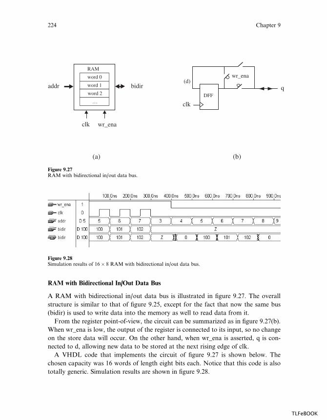
RAM with Bidirectional In/Out Data Bus
A RAM with bidirectional in/out data bus is illustrated in figure 9.27. The overall
structure is similar to that of figure 9.25, except for the fact that now the same bus
(bidir) is used to write data into the memory as well to read data from it.
From the register point-of-view, the circuit can be summarized as in figure 9.27(b).
When wr_ena is low, the output of the register is connected to its input, so no change
on the store data will occur. On the other hand, when wr_ena is asserted, q is con-
nected to d, allowing new data to be stored at the next rising edge of clk.
A VHDL code that implements the circuit of figure 9.27 is shown below. The
chosen capacity was 16 words of length eight bits each. Notice that this code is also
totally generic. Simulation results are shown in figure 9.28.
(a) (b)
bidir
RAM
word 0
word 1
word 2
…
clk
addr
clk
DFF
(d)q
wr_ena
wr_ena
Figure 9.27RAM with bidirectional in/out data bus.
Figure 9.28Simulation results of 16� 8 RAM with bidirectional in/out data bus.
224 Chapter 9
TLFeBOOK
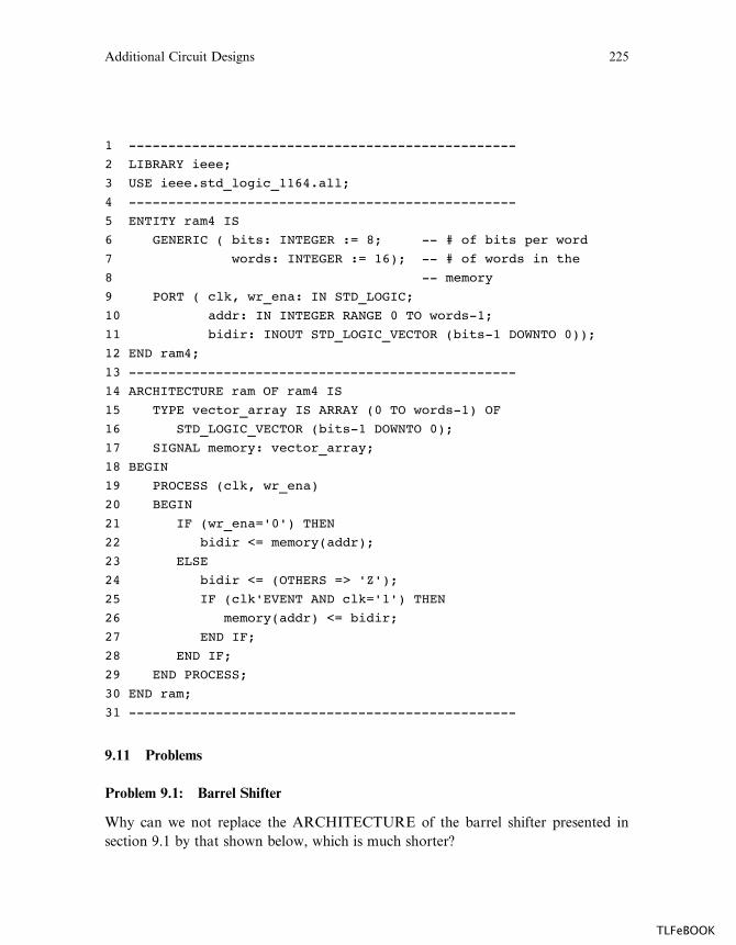
1 -------------------------------------------------
2 LIBRARY ieee;
3 USE ieee.std_logic_1164.all;
4 -------------------------------------------------
5 ENTITY ram4 IS
6 GENERIC ( bits: INTEGER := 8; -- # of bits per word
7 words: INTEGER := 16); -- # of words in the
8 -- memory
9 PORT ( clk, wr_ena: IN STD_LOGIC;
10 addr: IN INTEGER RANGE 0 TO words-1;
11 bidir: INOUT STD_LOGIC_VECTOR (bits-1 DOWNTO 0));
12 END ram4;
13 -------------------------------------------------
14 ARCHITECTURE ram OF ram4 IS
15 TYPE vector_array IS ARRAY (0 TO words-1) OF
16 STD_LOGIC_VECTOR (bits-1 DOWNTO 0);
17 SIGNAL memory: vector_array;
18 BEGIN
19 PROCESS (clk, wr_ena)
20 BEGIN
21 IF (wr_ena='0') THEN
22 bidir <= memory(addr);
23 ELSE
24 bidir <= (OTHERS => 'Z');
25 IF (clk'EVENT AND clk='1') THEN
26 memory(addr) <= bidir;
27 END IF;
28 END IF;
29 END PROCESS;
30 END ram;
31 -------------------------------------------------
9.11 Problems
Problem 9.1: Barrel Shifter
Why can we not replace the ARCHITECTURE of the barrel shifter presented in
section 9.1 by that shown below, which is much shorter?
Additional Circuit Designs 225
TLFeBOOK
---------------------------------------------
ARCHITECTURE barrel OF barrel IS
BEGIN
PROCESS (inp, shift)
BEGIN
IF (shift=0) THEN
outp <= inp;
ELSE
FOR i IN 0 TO shift-1 LOOP
outp(i) <= '0';
END LOOP;
FOR i IN shift TO inp'HIGH LOOP
outp(i) <= inp(i-1);
END LOOP;
END IF;
END PROCESS;
END barrel;
---------------------------------------------
Problem 9.2: Divider
In section 9.4, we studied the design of fixed-point dividers. Two solutions were pre-
sented, both using sequential statements (IF and LOOP). Moreover, the codes
implemented the second description of the division algorithm presented in that sec-
tion. You are asked to write a concurrent solution for the division problem (with
GENERATE). Additionally, your code should resemble the first description of the
division algorithm (figure 9.9). In order to do so, we suggest the creation and use of
the following types and signal:
SUBTYPE long IS STD_LOGIC_VECTOR (2n DOWNTO 0);
TYPE vec_array IS ARRAY (n DOWNTO 0) OF long;
SIGNAL a_input, b_input: vec_array;
where n should be declared as a GENERIC parameter.
Problem 9.3: Vending-Machine Controller
Consider the vending-machine controller designed in section 9.5. We want to intro-
duce some sophistications in it.
226 Chapter 9
TLFeBOOK
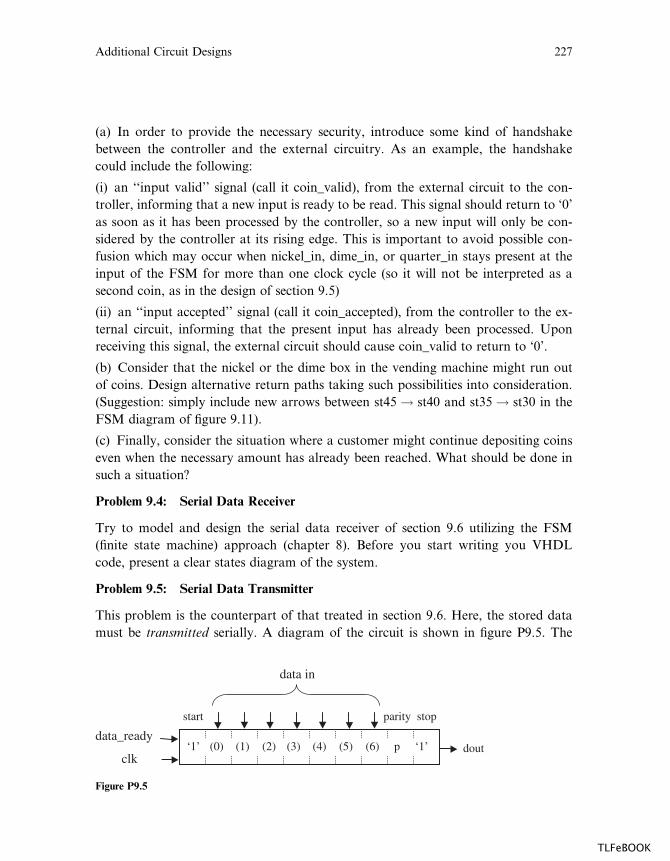
(a) In order to provide the necessary security, introduce some kind of handshake
between the controller and the external circuitry. As an example, the handshake
could include the following:
(i) an ‘‘input valid’’ signal (call it coin_valid), from the external circuit to the con-
troller, informing that a new input is ready to be read. This signal should return to ‘0’
as soon as it has been processed by the controller, so a new input will only be con-
sidered by the controller at its rising edge. This is important to avoid possible con-
fusion which may occur when nickel_in, dime_in, or quarter_in stays present at the
input of the FSM for more than one clock cycle (so it will not be interpreted as a
second coin, as in the design of section 9.5)
(ii) an ‘‘input accepted’’ signal (call it coin_accepted), from the controller to the ex-
ternal circuit, informing that the present input has already been processed. Upon
receiving this signal, the external circuit should cause coin_valid to return to ‘0’.
(b) Consider that the nickel or the dime box in the vending machine might run out
of coins. Design alternative return paths taking such possibilities into consideration.
(Suggestion: simply include new arrows between st45 ! st40 and st35 ! st30 in the
FSM diagram of figure 9.11).
(c) Finally, consider the situation where a customer might continue depositing coins
even when the necessary amount has already been reached. What should be done in
such a situation?
Problem 9.4: Serial Data Receiver
Try to model and design the serial data receiver of section 9.6 utilizing the FSM
(finite state machine) approach (chapter 8). Before you start writing you VHDL
code, present a clear states diagram of the system.
Problem 9.5: Serial Data Transmitter
This problem is the counterpart of that treated in section 9.6. Here, the stored data
must be transmitted serially. A diagram of the circuit is shown in figure P9.5. The
start parity stop
dout
data in
data_ready
clk‘1’ (0) (1) (2) (3) (4) (5) (6) p ‘1’
Figure P9.5
Additional Circuit Designs 227
TLFeBOOK

protocol is the same 10-bit structure of section 9.6; that is, a start bit (high), followed
by seven bits of actual data, plus a parity bit, computed such that the total number of
‘1’s in positions 2 to 9 is even, and finally a stop bit (also ‘1’). Consider that a
data_ready signal is available to inform when the data can be loaded into the regis-
ters and sent out.
Problem 9.6: Playing with an SSD
You are asked to introduce additional features in the little seven-segment display
(SSD) game of section 9.8.
(a) Add a 2-bit input, called ‘‘speed’’, which should be able to select four di¤erent
speeds for the circulatory movement. Keep the overlap time (time2) fixed at 30 ms,
changing only time1. Choose four di¤erent circulatory periods and physically verify
whether the circuit behaves as expected.
(b) Change the functionality of the stop input, such that instead of going to state
when a stop is asserted, it freezes in whatever state it was when stop was activated,
proceeding from there when stop returns to zero.
(c) Finally, add a ‘‘direction’’ pin. When low, the circuit should behave as above, but
when high, it should circulate in the opposite direction (counterclockwise).
(d) Physical verification: After synthesizing and simulating your design, physically
implement it in you PLD/FPGA development kit, following the steps below.
(i) First, verify in the report file generated by the compiler which pins of the chip
were assigned to the inputs (clock and switches) and to the outputs (SSD).
(ii) Next, connect the signal generator (set to 1 kHz, with the appropriate logic lev-
els, but leave it OFF while you make the connection) and the switches (which should
provide VDD and GND levels) to the inputs of the circuit (your development kit
board is normally equipped with test switches).
(iii) Connect the outputs of the chip to the SSD (your development kit board is
normally equipped with seven-segment displays).
(iv) Finally, download the compiled file from your computer to the development kit,
turn ON the signal generator, and verify the operation of your circuit. Play with the
switches in order to test all operation modes.
Problem 9.7: Speed Monitor
Figure P9.7 shows a possible view of a car speed monitor. The specifications of the
system are the following:
228 Chapter 9
TLFeBOOK
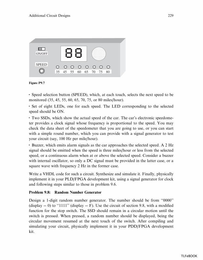
� Speed selection button (SPEED), which, at each touch, selects the next speed to be
monitored (35, 45, 55, 60, 65, 70, 75, or 80 miles/hour).
� Set of eight LEDs, one for each speed. The LED corresponding to the selected
speed should be ON.
� Two SSDs, which show the actual speed of the car. The car’s electronic speedome-
ter provides a clock signal whose frequency is proportional to the speed. You may
check the data sheet of the speedometer that you are going to use, or you can start
with a simple round number, which you can provide with a signal generator to test
your circuit (say, 100 Hz per mile/hour).
� Buzzer, which emits alarm signals as the car approaches the selected speed. A 2 Hz
signal should be emitted when the speed is three miles/hour or less from the selected
speed, or a continuous alarm when at or above the selected speed. Consider a buzzer
with internal oscillator, so only a DC signal must be provided in the latter case, or a
square wave with frequency 2 Hz in the former case.
Write a VHDL code for such a circuit. Synthesize and simulate it. Finally, physically
implement it in your PLD/FPGA development kit, using a signal generator for clock
and following steps similar to those in problem 9.6.
Problem 9.8: Random Number Generator
Design a 1-digit random number generator. The number should be from ‘‘0000’’
(display ¼ 0) to ‘‘1111’’ (display ¼ F). Use the circuit of section 9.8, with a modified
function for the stop switch. The SSD should remain in a circular motion until the
switch is pressed. When pressed, a random number should be displayed, being the
circular movement resumed at the next touch of the switch. After compiling and
simulating your circuit, physically implement it in your PDD/FPGA development
kit.
35 45 55 60 65 70 75 80
SPEED
ON/OFF
Figure P9.7
Additional Circuit Designs 229
TLFeBOOK

TLFeBOOK

II SYSTEM DESIGN
TLFeBOOK

TLFeBOOK

10 Packages and Components
10.1 Introduction
In Part I of the book, we studied the entire background and coding techniques of
VHDL, which included the following:
� Code structure: library declarations, entity, architecture (chapter 2)
� Data types (chapter 3)
� Operators and attributes (chapter 4)
� Concurrent statements and concurrent code (chapter 5)
� Sequential statements and sequential code (chapter 6)
� Signals, variables, and constants (chapter 7)
� Design of finite state machines (chapter 8)
� Additional circuit designs (chapter 9)
Thus, in terms of figure 10.1, we may say that we have covered in detail all that is
needed to construct the type of code depicted on its left-hand side. A good under-
standing of that material is indispensable, regardless of the design being just a small
circuit or a very large system.
In Part II, we will simply add new building blocks to the material already pre-
sented. These new building blocks are intended mainly for library allocation, being
shown on the right-hand side of figure 10.1. They are:
� Packages (chapter 10)
� Components (chapter 10)
� Functions (chapter 11)
� Procedures (chapter 11)
These new units can be located in the main code itself (that is, on the left-hand side
of figure 10.1). However, since their main purpose is to allow common pieces of code
to be reused and shared, it is more usual to place them in a LIBRARY. This also
leads to code partitioning, which is helpful when dealing with long codes. In sum-
mary, frequently used pieces of code can be written in the form of COMPONENTS,
FUNCTIONS, or PROCEDURES, then placed in a PACKAGE, which is finally
compiled into the destination LIBRARY.
We have already seen (chapter 2) that at least three LIBRARIES are generally
needed in a design: ieee, std, and work. After studying Part II, we will be able to
construct our own libraries, which can then be added to the list above.
TLFeBOOK
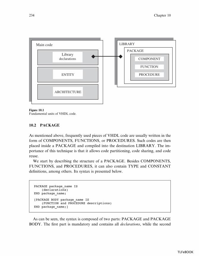
10.2 PACKAGE
As mentioned above, frequently used pieces of VHDL code are usually written in the
form of COMPONENTS, FUNCTIONS, or PROCEDURES. Such codes are then
placed inside a PACKAGE and compiled into the destination LIBRARY. The im-
portance of this technique is that it allows code partitioning, code sharing, and code
reuse.
We start by describing the structure of a PACKAGE. Besides COMPONENTS,
FUNCTIONS, and PROCEDURES, it can also contain TYPE and CONSTANT
definitions, among others. Its syntax is presented below.
PACKAGE package_name IS(declarations)
END package_name;
[PACKAGE BODY package_name IS(FUNCTION and PROCEDURE descriptions)
END package_name;]
As can be seen, the syntax is composed of two parts: PACKAGE and PACKAGE
BODY. The first part is mandatory and contains all declarations, while the second
Librarydeclarations
ENTITY
ARCHITECTURE
Main code LIBRARY
PACKAGE
FUNCTION
COMPONENT
PROCEDURE
Figure 10.1Fundamental units of VHDL code.
234 Chapter 10
TLFeBOOK
part is necessary only when one or more subprograms (FUNCTION or PROCE-
DURE) are declared in the upper part, in which case it must contain the descriptions
(bodies) of the subprograms. PACKAGE and PACKAGE BODY must have the
same name.
The declarations list can contain the following: COMPONENT, FUNCTION,
PROCEDURE, TYPE, CONSTANT, etc.
Example 10.1: Simple Package
The example below shows a PACKAGE called my_package. It contains only TYPE
and CONSTANT declarations, so a PACKAGE BODY is not necessary.
1 ------------------------------------------------
2 LIBRARY ieee;
3 USE ieee.std_logic_1164.all;
4 ------------------------------------------------
5 PACKAGE my_package IS
6 TYPE state IS (st1, st2, st3, st4);
7 TYPE color IS (red, green, blue);
8 CONSTANT vec: STD_LOGIC_VECTOR(7 DOWNTO 0) := "11111111";
9 END my_package;
10 ------------------------------------------------
Example 10.2: Package with a Function
This example contains, besides TYPE and CONSTANT declarations, a FUNC-
TION. Therefore, a PACKAGE BODY is now needed (details on how to write a
FUNCTION will be seen in chapter 11). This function returns TRUE when a posi-
tive edge occurs on clk.
1 -------------------------------------------------
2 LIBRARY ieee;
3 USE ieee.std_logic_1164.all;
4 -------------------------------------------------
5 PACKAGE my_package IS
6 TYPE state IS (st1, st2, st3, st4);
7 TYPE color IS (red, green, blue);
8 CONSTANT vec: STD_LOGIC_VECTOR(7 DOWNTO 0) := "11111111";
9 FUNCTION positive_edge(SIGNAL s: STD_LOGIC) RETURN BOOLEAN;
10 END my_package;
Packages and Components 235
TLFeBOOK
11 -------------------------------------------------
12 PACKAGE BODY my_package IS
13 FUNCTION positive_edge(SIGNAL s: STD_LOGIC) RETURN BOOLEAN IS
14 BEGIN
15 RETURN (s'EVENT AND s='1');
16 END positive_edge;
17 END my_package;
18 -------------------------------------------------
Any of the PACKAGES above (example 10.1 or example 10.2) can now be
compiled, becoming then part of our work LIBRARY (or any other). To make use
of it in a VHDL code, we have to add a new USE clause to the main code (USE
work.my_package.all), as shown below.
------------------------------------
LIBRARY ieee;
USE ieee.std_logic_1164.all;
USE work.my_package.all;
------------------------------------
ENTITY...
...
ARCHITECTURE...
...
------------------------------------
10.3 COMPONENT
A COMPONENT is simply a piece of conventional code (that is, LIBRARY
declarationsþ ENTITYþARCHITECTURE, as seen in chapter 2). However, by
declaring such code as being a COMPONENT, it can then be used within another
circuit, thus allowing the construction of hierarchical designs.
A COMPONENT is also another way of partitioning a code and providing code
sharing and code reuse. For example, commonly used circuits, like flip-flops, multi-
plexers, adders, basic gates, etc., can be placed in a LIBRARY, so any project can
make use of them without having to explicitly rewrite such codes.
To use (instantiate) a COMPONENT, it must first be declared. The corresponding
syntaxes are shown below.
236 Chapter 10
TLFeBOOK

COMPONENT declaration:
COMPONENT component_name ISPORT (
port_name : signal_mode signal_type;port_name : signal_mode signal_type;...);
END COMPONENT;
COMPONENT instantiation:
label: component_name PORT MAP (port_list);
As can be seen, the syntax of the declaration is similar to that of an ENTITY
(section 2.3); that is, the names of the ports must be specified, along with their modes
(IN, OUT, BUFFER, or INOUT) and data types (STD_LOGIC_VECTOR, IN-
TEGER, BOOLEAN, etc.). To instantiate a component a label is required, followed
by the component’s name and a PORT MAP declaration. Finally, port_list is just a
list relating the ports of the actual circuit to the ports of the pre-designed component
which is being instantiated.
Example: Let us consider an inverter, which has been previously designed
(inverter.vhd) and compiled into the work library. We can make use of it by means
of the code shown below. The label chosen for this component was U1. The names of
the ports in the actual circuit are x and y, which are being assigned to a and b, re-
spectively, of the pre-designed inverter (this is called positional mapping, for the first
signal in one corresponds to the first signal in the other, the second in one to the
second in the other, and so on).
----- COMPONENT declaration: -----------
COMPONENT inverter IS
PORT (a: IN STD_LOGIC; b: OUT STD_LOGIC);
END COMPONENT;
----- COMPONENT instantiation: -----------
U1: inverter PORT MAP (x, y);
There are two basic ways to declare a COMPONENT (figure 10.2). Once we have
designed it and placed it in the destination LIBRARY, we can declare it in the
Packages and Components 237
TLFeBOOK
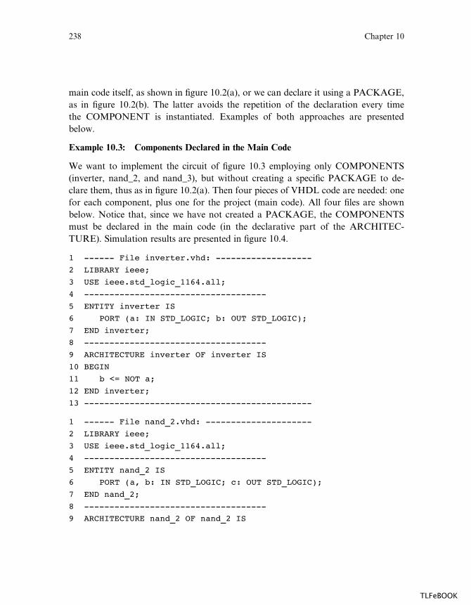
main code itself, as shown in figure 10.2(a), or we can declare it using a PACKAGE,
as in figure 10.2(b). The latter avoids the repetition of the declaration every time
the COMPONENT is instantiated. Examples of both approaches are presented
below.
Example 10.3: Components Declared in the Main Code
We want to implement the circuit of figure 10.3 employing only COMPONENTS
(inverter, nand_2, and nand_3), but without creating a specific PACKAGE to de-
clare them, thus as in figure 10.2(a). Then four pieces of VHDL code are needed: one
for each component, plus one for the project (main code). All four files are shown
below. Notice that, since we have not created a PACKAGE, the COMPONENTS
must be declared in the main code (in the declarative part of the ARCHITEC-
TURE). Simulation results are presented in figure 10.4.
1 ------ File inverter.vhd: -------------------
2 LIBRARY ieee;
3 USE ieee.std_logic_1164.all;
4 ------------------------------------
5 ENTITY inverter IS
6 PORT (a: IN STD_LOGIC; b: OUT STD_LOGIC);
7 END inverter;
8 ------------------------------------
9 ARCHITECTURE inverter OF inverter IS
10 BEGIN
11 b <= NOT a;
12 END inverter;
13 ---------------------------------------------
1 ------ File nand_2.vhd: ---------------------
2 LIBRARY ieee;
3 USE ieee.std_logic_1164.all;
4 ------------------------------------
5 ENTITY nand_2 IS
6 PORT (a, b: IN STD_LOGIC; c: OUT STD_LOGIC);
7 END nand_2;
8 ------------------------------------
9 ARCHITECTURE nand_2 OF nand_2 IS
238 Chapter 10
TLFeBOOK
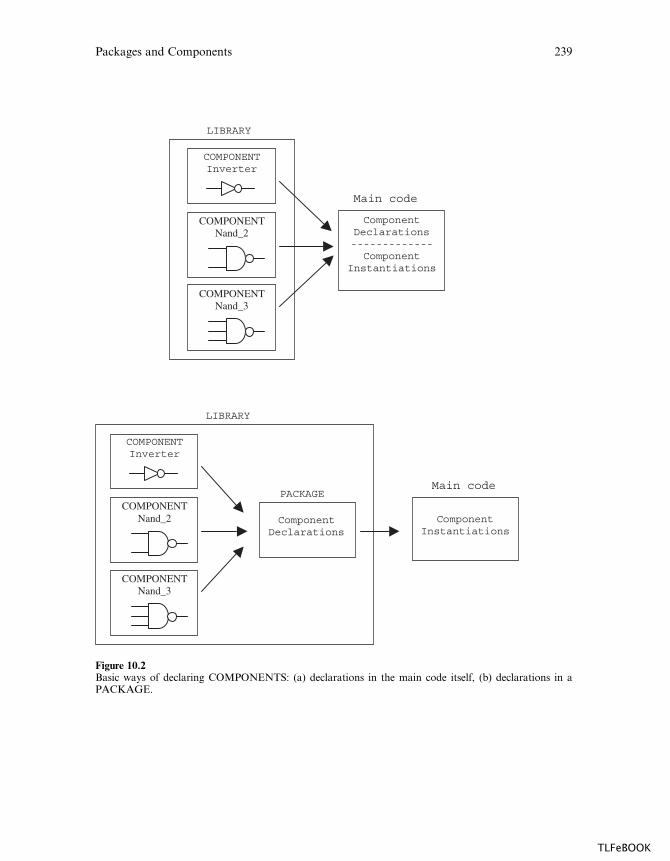
ComponentDeclarations-------------Component
Instantiations
Main code
COMPONENTInverter
COMPONENTNand_2
COMPONENTNand_3
LIBRARY
ComponentInstantiations
Main code
COMPONENTInverter
COMPONENTNand_2
COMPONENTNand_3
LIBRARY
PACKAGE
ComponentDeclarations
Figure 10.2Basic ways of declaring COMPONENTS: (a) declarations in the main code itself, (b) declarations in aPACKAGE.
Packages and Components 239
TLFeBOOK
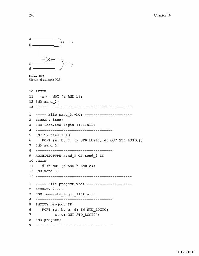
10 BEGIN
11 c <= NOT (a AND b);
12 END nand_2;
13 ---------------------------------------------
1 ----- File nand_3.vhd: ----------------------
2 LIBRARY ieee;
3 USE ieee.std_logic_1164.all;
4 ------------------------------------
5 ENTITY nand_3 IS
6 PORT (a, b, c: IN STD_LOGIC; d: OUT STD_LOGIC);
7 END nand_3;
8 ------------------------------------
9 ARCHITECTURE nand_3 OF nand_3 IS
10 BEGIN
11 d <= NOT (a AND b AND c);
12 END nand_3;
13 ---------------------------------------------
1 ----- File project.vhd: ---------------------
2 LIBRARY ieee;
3 USE ieee.std_logic_1164.all;
4 ------------------------------------
5 ENTITY project IS
6 PORT (a, b, c, d: IN STD_LOGIC;
7 x, y: OUT STD_LOGIC);
8 END project;
9 ------------------------------------
x
y
a
b
c
d
Figure 10.3Circuit of example 10.3.
240 Chapter 10
TLFeBOOK
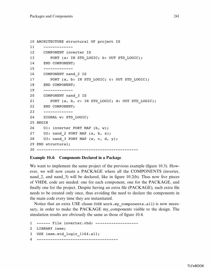
10 ARCHITECTURE structural OF project IS
11 -------------
12 COMPONENT inverter IS
13 PORT (a: IN STD_LOGIC; b: OUT STD_LOGIC);
14 END COMPONENT;
15 -------------
16 COMPONENT nand_2 IS
17 PORT (a, b: IN STD_LOGIC; c: OUT STD_LOGIC);
18 END COMPONENT;
19 -------------
20 COMPONENT nand_3 IS
21 PORT (a, b, c: IN STD_LOGIC; d: OUT STD_LOGIC);
22 END COMPONENT;
23 -------------
24 SIGNAL w: STD_LOGIC;
25 BEGIN
26 U1: inverter PORT MAP (b, w);
27 U2: nand_2 PORT MAP (a, b, x);
28 U3: nand_3 PORT MAP (w, c, d, y);
29 END structural;
30 ---------------------------------------------
Example 10.4: Components Declared in a Package
We want to implement the same project of the previous example (figure 10.3). How-
ever, we will now create a PACKAGE where all the COMPONENTS (inverter,
nand_2, and nand_3) will be declared, like in figure 10.2(b). Thus now five pieces
of VHDL code are needed: one for each component, one for the PACKAGE, and
finally one for the project. Despite having an extra file (PACKAGE), such extra file
needs to be created only once, thus avoiding the need to declare the components in
the main code every time they are instantiated.
Notice that an extra USE clause (USE work.my_components.all) is now neces-
sary, in order to make the PACKAGE my_components visible to the design. The
simulation results are obviously the same as those of figure 10.4.
1 ------ File inverter.vhd: -------------------
2 LIBRARY ieee;
3 USE ieee.std_logic_1164.all;
4 ------------------------------------
Packages and Components 241
TLFeBOOK
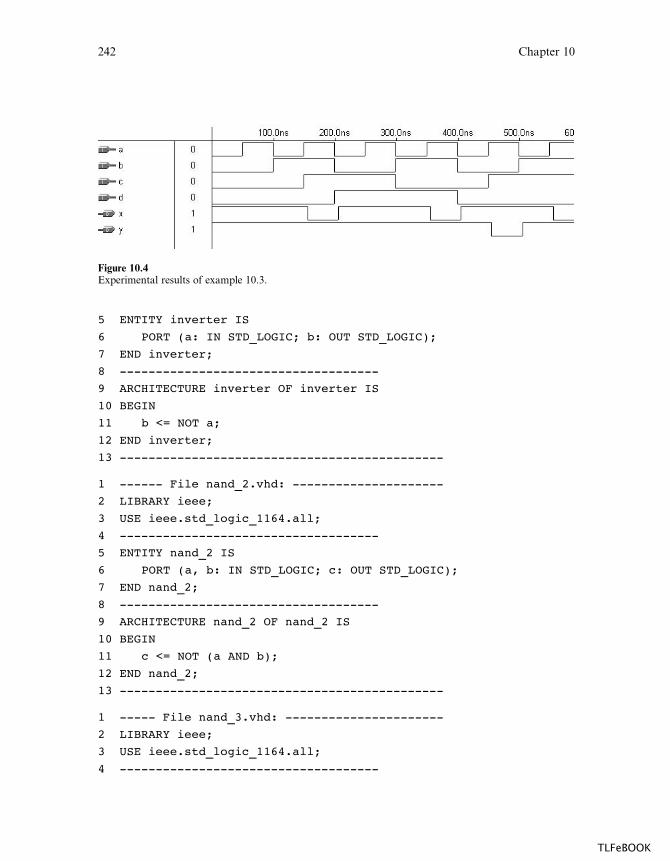
5 ENTITY inverter IS
6 PORT (a: IN STD_LOGIC; b: OUT STD_LOGIC);
7 END inverter;
8 ------------------------------------
9 ARCHITECTURE inverter OF inverter IS
10 BEGIN
11 b <= NOT a;
12 END inverter;
13 ---------------------------------------------
1 ------ File nand_2.vhd: ---------------------
2 LIBRARY ieee;
3 USE ieee.std_logic_1164.all;
4 ------------------------------------
5 ENTITY nand_2 IS
6 PORT (a, b: IN STD_LOGIC; c: OUT STD_LOGIC);
7 END nand_2;
8 ------------------------------------
9 ARCHITECTURE nand_2 OF nand_2 IS
10 BEGIN
11 c <= NOT (a AND b);
12 END nand_2;
13 ---------------------------------------------
1 ----- File nand_3.vhd: ----------------------
2 LIBRARY ieee;
3 USE ieee.std_logic_1164.all;
4 ------------------------------------
Figure 10.4Experimental results of example 10.3.
242 Chapter 10
TLFeBOOK
5 ENTITY nand_3 IS
6 PORT (a, b, c: IN STD_LOGIC; d: OUT STD_LOGIC);
7 END nand_3;
8 ------------------------------------
9 ARCHITECTURE nand_3 OF nand_3 IS
10 BEGIN
11 d <= NOT (a AND b AND c);
12 END nand_3;
13 ---------------------------------------------
1 ----- File my_components.vhd: ---------------
2 LIBRARY ieee;
3 USE ieee.std_logic_1164.all;
4 ------------------------
5 PACKAGE my_components IS
6 ------ inverter: -------
7 COMPONENT inverter IS
8 PORT (a: IN STD_LOGIC; b: OUT STD_LOGIC);
9 END COMPONENT;
10 ------ 2-input nand: ---
11 COMPONENT nand_2 IS
12 PORT (a, b: IN STD_LOGIC; c: OUT STD_LOGIC);
13 END COMPONENT;
14 ------ 3-input nand: ---
15 COMPONENT nand_3 IS
16 PORT (a, b, c: IN STD_LOGIC; d: OUT STD_LOGIC);
17 END COMPONENT;
18 ------------------------
19 END my_components;
20 ---------------------------------------------
1 ----- File project.vhd: ---------------------
2 LIBRARY ieee;
3 USE ieee.std_logic_1164.all;
4 USE work.my_components.all;
5 ---------------------------------
6 ENTITY project IS
7 PORT ( a, b, c, d: IN STD_LOGIC;
8 x, y: OUT STD_LOGIC);
Packages and Components 243
TLFeBOOK
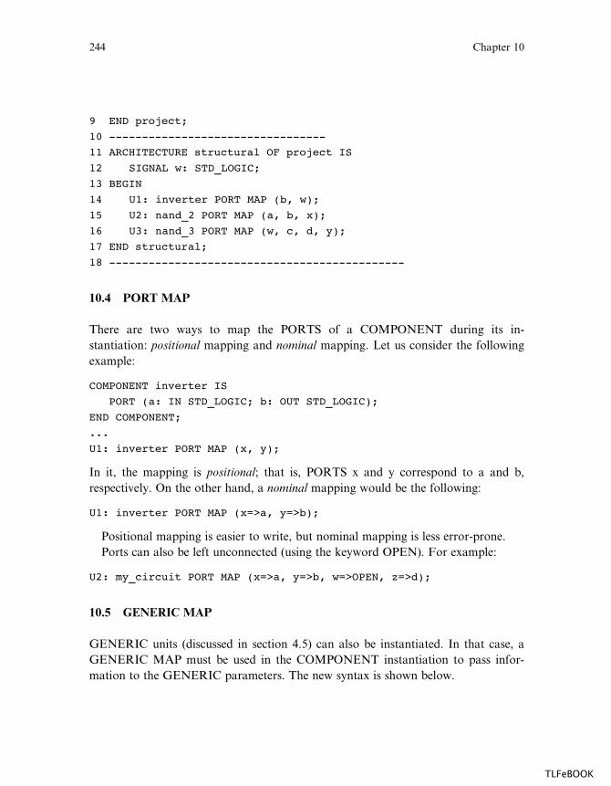
9 END project;
10 ---------------------------------
11 ARCHITECTURE structural OF project IS
12 SIGNAL w: STD_LOGIC;
13 BEGIN
14 U1: inverter PORT MAP (b, w);
15 U2: nand_2 PORT MAP (a, b, x);
16 U3: nand_3 PORT MAP (w, c, d, y);
17 END structural;
18 ---------------------------------------------
10.4 PORT MAP
There are two ways to map the PORTS of a COMPONENT during its in-
stantiation: positional mapping and nominal mapping. Let us consider the following
example:
COMPONENT inverter IS
PORT (a: IN STD_LOGIC; b: OUT STD_LOGIC);
END COMPONENT;
...
U1: inverter PORT MAP (x, y);
In it, the mapping is positional; that is, PORTS x and y correspond to a and b,
respectively. On the other hand, a nominal mapping would be the following:
U1: inverter PORT MAP (x=>a, y=>b);
Positional mapping is easier to write, but nominal mapping is less error-prone.
Ports can also be left unconnected (using the keyword OPEN). For example:
U2: my_circuit PORT MAP (x=>a, y=>b, w=>OPEN, z=>d);
10.5 GENERIC MAP
GENERIC units (discussed in section 4.5) can also be instantiated. In that case, a
GENERIC MAP must be used in the COMPONENT instantiation to pass infor-
mation to the GENERIC parameters. The new syntax is shown below.
244 Chapter 10
TLFeBOOK
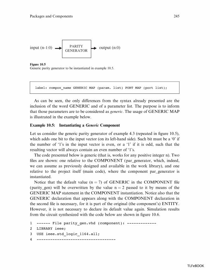
label: compon_name GENERIC MAP (param. list) PORT MAP (port list);
As can be seen, the only di¤erences from the syntax already presented are the
inclusion of the word GENERIC and of a parameter list. The purpose is to inform
that those parameters are to be considered as generic. The usage of GENERIC MAP
is illustrated in the example below.
Example 10.5: Instantiating a Generic Component
Let us consider the generic parity generator of example 4.3 (repeated in figure 10.5),
which adds one bit to the input vector (on its left-hand side). Such bit must be a ‘0’ if
the number of ‘1’s in the input vector is even, or a ‘1’ if it is odd, such that the
resulting vector will always contain an even number of ‘1’s.
The code presented below is generic (that is, works for any positive integer n). Two
files are shown: one relative to the COMPONENT (par_generator, which, indeed,
we can assume as previously designed and available in the work library), and one
relative to the project itself (main code), where the component par_generator is
instantiated.
Notice that the default value (n ¼ 7) of GENERIC in the COMPONENT file
(parity_gen) will be overwritten by the value n ¼ 2 passed to it by means of the
GENERIC MAP statement in the COMPONENT instantiation. Notice also that the
GENERIC declaration that appears along with the COMPONENT declaration in
the second file is necessary, for it is part of the original (the component’s) ENTITY.
However, it is not necessary to declare its default value again. Simulation results
from the circuit synthesized with the code below are shown in figure 10.6.
1 ------ File parity_gen.vhd (component): -------------
2 LIBRARY ieee;
3 USE ieee.std_logic_1164.all;
4 -----------------------------------
input (n-1:0) PARITYGENERATOR
output (n:0)
Figure 10.5Generic parity generator to be instantiated in example 10.5.
Packages and Components 245
TLFeBOOK
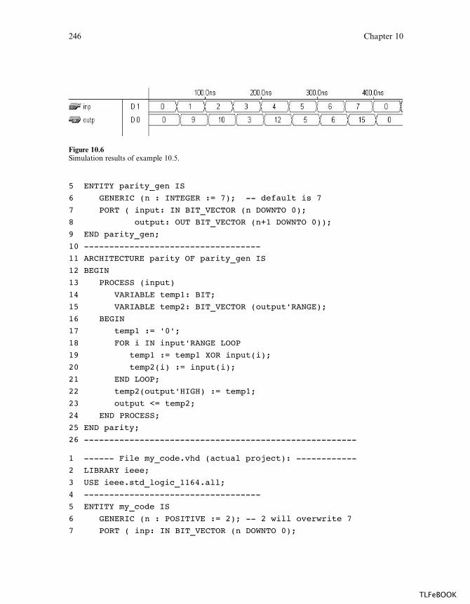
5 ENTITY parity_gen IS
6 GENERIC (n : INTEGER := 7); -- default is 7
7 PORT ( input: IN BIT_VECTOR (n DOWNTO 0);
8 output: OUT BIT_VECTOR (n+1 DOWNTO 0));
9 END parity_gen;
10 -----------------------------------
11 ARCHITECTURE parity OF parity_gen IS
12 BEGIN
13 PROCESS (input)
14 VARIABLE temp1: BIT;
15 VARIABLE temp2: BIT_VECTOR (output'RANGE);
16 BEGIN
17 temp1 := '0';
18 FOR i IN input'RANGE LOOP
19 temp1 := temp1 XOR input(i);
20 temp2(i) := input(i);
21 END LOOP;
22 temp2(output'HIGH) := temp1;
23 output <= temp2;
24 END PROCESS;
25 END parity;
26 ------------------------------------------------------
1 ------ File my_code.vhd (actual project): ------------
2 LIBRARY ieee;
3 USE ieee.std_logic_1164.all;
4 -----------------------------------
5 ENTITY my_code IS
6 GENERIC (n : POSITIVE := 2); -- 2 will overwrite 7
7 PORT ( inp: IN BIT_VECTOR (n DOWNTO 0);
Figure 10.6Simulation results of example 10.5.
246 Chapter 10
TLFeBOOK
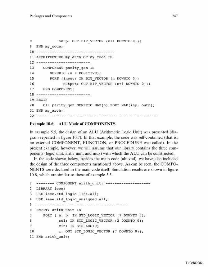
8 outp: OUT BIT_VECTOR (n+1 DOWNTO 0));
9 END my_code;
10 -----------------------------------
11 ARCHITECTURE my_arch OF my_code IS
12 ------------------------
13 COMPONENT parity_gen IS
14 GENERIC (n : POSITIVE);
15 PORT (input: IN BIT_VECTOR (n DOWNTO 0);
16 output: OUT BIT_VECTOR (n+1 DOWNTO 0));
17 END COMPONENT;
18 ------------------------
19 BEGIN
20 C1: parity_gen GENERIC MAP(n) PORT MAP(inp, outp);
21 END my_arch;
22 ------------------------------------------------------
Example 10.6: ALU Made of COMPONENTS
In example 5.5, the design of an ALU (Arithmetic Logic Unit) was presented (dia-
gram repeated in figure 10.7). In that example, the code was self-contained (that is,
no external COMPONENT, FUNCTION, or PROCEDURE was called). In the
present example, however, we will assume that our library contains the three com-
ponents (logic_unit, arith_unit, and mux) with which the ALU can be constructed.
In the code shown below, besides the main code (alu.vhd), we have also included
the design of the three components mentioned above. As can be seen, the COMPO-
NENTS were declared in the main code itself. Simulation results are shown in figure
10.8, which are similar to those of example 5.5.
1 -------- COMPONENT arith_unit: --------------------
2 LIBRARY ieee;
3 USE ieee.std_logic_1164.all;
4 USE ieee.std_logic_unsigned.all;
5 -----------------------------------------
6 ENTITY arith_unit IS
7 PORT ( a, b: IN STD_LOGIC_VECTOR (7 DOWNTO 0);
8 sel: IN STD_LOGIC_VECTOR (2 DOWNTO 0);
9 cin: IN STD_LOGIC;
10 x: OUT STD_LOGIC_VECTOR (7 DOWNTO 0));
11 END arith_unit;
Packages and Components 247
TLFeBOOK
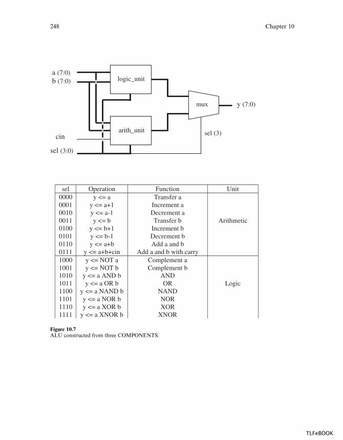
sel Operation Function Unit00000001001000110100010101100111
y <= ay <= a+1y <= a-1y <= b
y <= b+1y <= b-1y <= a+b
y <= a+b+cin
Transfer aIncrement aDecrement aTransfer b
Increment bDecrement bAdd a and b
Add a and b with carry
Arithmetic
10001001101010111100110111101111
y <= NOT ay <= NOT b
y <= a AND by <= a OR b
y <= a NAND by <= a NOR by <= a XOR b
y <= a XNOR b
Complement aComplement b
ANDOR
NANDNORXOR
XNOR
Logic
sel (3)
a (7:0)b (7:0)
cin
sel (3:0)
logic_unit
arith_unit
mux y (7:0)
Figure 10.7ALU constructed from three COMPONENTS.
248 Chapter 10
TLFeBOOK
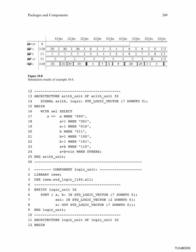
12 -----------------------------------------
13 ARCHITECTURE arith_unit OF arith_unit IS
14 SIGNAL arith, logic: STD_LOGIC_VECTOR (7 DOWNTO 0);
15 BEGIN
16 WITH sel SELECT
17 x <= a WHEN "000",
18 a+1 WHEN "001",
19 a-1 WHEN "010",
20 b WHEN "011",
21 b+1 WHEN "100",
22 b-1 WHEN "101",
23 a+b WHEN "110",
24 a+b+cin WHEN OTHERS;
25 END arith_unit;
26 ---------------------------------------------------
1 -------- COMPONENT logic_unit: --------------------
2 LIBRARY ieee;
3 USE ieee.std_logic_1164.all;
4 -----------------------------------------
5 ENTITY logic_unit IS
6 PORT ( a, b: IN STD_LOGIC_VECTOR (7 DOWNTO 0);
7 sel: IN STD_LOGIC_VECTOR (2 DOWNTO 0);
8 x: OUT STD_LOGIC_VECTOR (7 DOWNTO 0));
9 END logic_unit;
10 -----------------------------------------
11 ARCHITECTURE logic_unit OF logic_unit IS
12 BEGIN
Figure 10.8Simulation results of example 10.6.
Packages and Components 249
TLFeBOOK

13 WITH sel SELECT
14 x <= NOT a WHEN "000",
15 NOT b WHEN "001",
16 a AND b WHEN "010",
17 a OR b WHEN "011",
18 a NAND b WHEN "100",
19 a NOR b WHEN "101",
20 a XOR b WHEN "110",
21 NOT (a XOR b) WHEN OTHERS;
22 END logic_unit;
23 ---------------------------------------------------
1 -------- COMPONENT mux: ---------------------------
2 LIBRARY ieee;
3 USE ieee.std_logic_1164.all;
4 -----------------------------------------
5 ENTITY mux IS
6 PORT ( a, b: IN STD_LOGIC_VECTOR (7 DOWNTO 0);
7 sel: IN STD_LOGIC;
8 x: OUT STD_LOGIC_VECTOR (7 DOWNTO 0));
9 END mux;
10 -----------------------------------------
11 ARCHITECTURE mux OF mux IS
12 BEGIN
13 WITH sel SELECT
14 x <= a WHEN '0',
15 b WHEN OTHERS;
16 END mux;
17 ---------------------------------------------------
1 -------- Project ALU (main code): -----------------
2 LIBRARY ieee;
3 USE ieee.std_logic_1164.all;
4 -----------------------------------------
5 ENTITY alu IS
6 PORT ( a, b: IN STD_LOGIC_VECTOR(7 DOWNTO 0);
7 cin: IN STD_LOGIC;
8 sel: IN STD_LOGIC_VECTOR(3 DOWNTO 0);
9 y: OUT STD_LOGIC_VECTOR(7 DOWNTO 0));
250 Chapter 10
TLFeBOOK

10 END alu;
11 -----------------------------------------
12 ARCHITECTURE alu OF alu IS
13 -----------------------
14 COMPONENT arith_unit IS
15 PORT ( a, b: IN STD_LOGIC_VECTOR(7 DOWNTO 0);
16 cin: IN STD_LOGIC;
17 sel: IN STD_LOGIC_VECTOR(2 DOWNTO 0);
18 x: OUT STD_LOGIC_VECTOR(7 DOWNTO 0));
19 END COMPONENT;
20 -----------------------
21 COMPONENT logic_unit IS
22 PORT ( a, b: IN STD_LOGIC_VECTOR(7 DOWNTO 0);
23 sel: IN STD_LOGIC_VECTOR(2 DOWNTO 0);
24 x: OUT STD_LOGIC_VECTOR(7 DOWNTO 0));
25 END COMPONENT;
26 -----------------------
27 COMPONENT mux IS
28 PORT ( a, b: IN STD_LOGIC_VECTOR(7 DOWNTO 0);
29 sel: IN STD_LOGIC;
30 x: OUT STD_LOGIC_VECTOR(7 DOWNTO 0));
31 END COMPONENT;
32 -----------------------
33 SIGNAL x1, x2: STD_LOGIC_VECTOR(7 DOWNTO 0);
34 -----------------------
35 BEGIN
36 U1: arith_unit PORT MAP (a, b, cin, sel(2 DOWNTO 0), x1);
37 U2: logic_unit PORT MAP (a, b, sel(2 DOWNTO 0), x2);
38 U3: mux PORT MAP (x1, x2, sel(3), y);
39 END alu;
40 ---------------------------------------------------
10.6 Problems
Problem 10.1: ALU with Components Declared in a Package
Redo example 10.6. This time, create a PACKAGE containing all COMPONENT
declarations. Then make the changes needed in the main code and recompile it.
Synthesize and simulate your solution to fully verify its functionality.
Packages and Components 251
TLFeBOOK
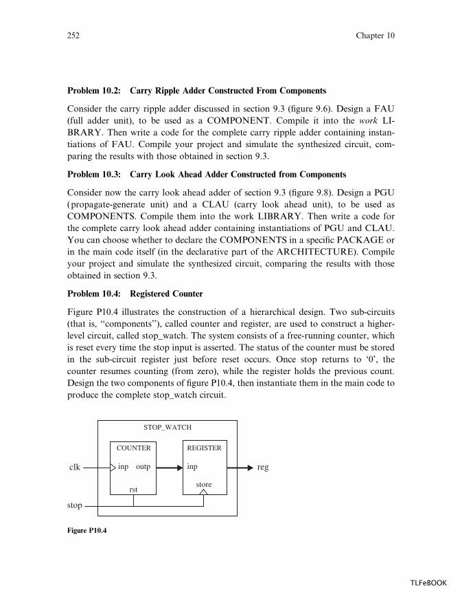
Problem 10.2: Carry Ripple Adder Constructed From Components
Consider the carry ripple adder discussed in section 9.3 (figure 9.6). Design a FAU
(full adder unit), to be used as a COMPONENT. Compile it into the work LI-
BRARY. Then write a code for the complete carry ripple adder containing instan-
tiations of FAU. Compile your project and simulate the synthesized circuit, com-
paring the results with those obtained in section 9.3.
Problem 10.3: Carry Look Ahead Adder Constructed from Components
Consider now the carry look ahead adder of section 9.3 (figure 9.8). Design a PGU
(propagate-generate unit) and a CLAU (carry look ahead unit), to be used as
COMPONENTS. Compile them into the work LIBRARY. Then write a code for
the complete carry look ahead adder containing instantiations of PGU and CLAU.
You can choose whether to declare the COMPONENTS in a specific PACKAGE or
in the main code itself (in the declarative part of the ARCHITECTURE). Compile
your project and simulate the synthesized circuit, comparing the results with those
obtained in section 9.3.
Problem 10.4: Registered Counter
Figure P10.4 illustrates the construction of a hierarchical design. Two sub-circuits
(that is, ‘‘components’’), called counter and register, are used to construct a higher-
level circuit, called stop_watch. The system consists of a free-running counter, which
is reset every time the stop input is asserted. The status of the counter must be stored
in the sub-circuit register just before reset occurs. Once stop returns to ‘0’, the
counter resumes counting (from zero), while the register holds the previous count.
Design the two components of figure P10.4, then instantiate them in the main code to
produce the complete stop_watch circuit.
clk
stop
store
inp
REGISTERCOUNTER
rst
STOP_WATCH
inp outp reg
Figure P10.4
252 Chapter 10
TLFeBOOK

11Functions and Procedures
FUNCTIONS and PROCEDURES are collectively called subprograms. From a
construction point of view, they are very similar to a PROCESS (studied in chapter
6), for they are the only pieces of sequential VHDL code, and thus employ the same
sequential statements seen there (IF, CASE, and LOOP; WAIT is not allowed).
However, from the applications point of view, there is a fundamental di¤erence be-
tween a PROCESS and a FUNCTION or PROCEDURE. While the first is intended
for immediate use in the main code, the others are intended mainly for LIBRARY
allocation, that is, their purpose is to store commonly used pieces of code, so they
can be reused or shared by other projects. Nevertheless, if desired, a FUNCTION or
PROCEDURE can also be installed in the main code itself.
11.1 FUNCTION
A FUNCTION is a section of sequential code. Its purpose is to create new functions
to deal with commonly encountered problems, like data type conversions, logical
operations, arithmetic computations, and new operators and attributes. By writing
such code as a FUNCTION, it can be shared and reused, also propitiating the main
code to be shorter and easier to understand.
As already mentioned, a FUNCTION is very similar to a PROCESS (section 6.1).
The same statements that can be used in a process (IF, WAIT, CASE, and LOOP)
can also be used in a function, with the exception of WAIT. Other two prohibitions
in a function are SIGNAL declarations and COMPONENT instantiations.
To construct and use a function, two parts are necessary: the function itself (func-
tion body) and a call to the function. Their syntaxes are shown below.
Function Body
FUNCTION function_name [<parameter list>] RETURN data_type IS[declarations]
BEGIN(sequential statements)
END function_name;
In the syntax above, 3parameter list4 specifies the function’s input parameters,
that is:
3parameter list4 ¼ [CONSTANT] constant_name: constant_type; or
3parameter list4 ¼ SIGNAL signal_name: signal_type;
TLFeBOOK

There can be any number of such parameters (even zero), which, as shown above,
can only be CONSTANT (default) or SIGNAL (VARIABLES are not allowed).
Their types can be any of the synthesizable data types studied in chapter 3 (BOO-
LEAN, STD_LOGIC, INTEGER, etc.). However, no range specification should be
included (for example, do not enter RANGE when using INTEGER, or TO/
DOWNTO when using STD_LOGIC_VECTOR). On the other hand, there is only
one return value, whose type is specified by data_type.
Example: The function below, named f1, receives three parameters (a, b, and
c). a and b are CONSTANTS (notice that the word CONSTANT can be omitted,
for it is the default object), while c is a SIGNAL. a and b are of type INTEGER,
while c is of type STD_LOGIC_VECTOR. Notice that neither RANGE nor
DOWNTO was specified. The output parameter (there can be only one) is of type
BOOLEAN.
FUNCTION f1 (a, b: INTEGER; SIGNAL c: STD_LOGIC_VECTOR)
RETURN BOOLEAN IS
BEGIN
(sequential statements)
END f1;
Function Call
A function is called as part of an expression. The expression can obviously appear by
itself or associated to a statement (either concurrent or sequential).
Examples of function calls:
x <= conv_integer(a); -- converts a to an integer
-- (expression appears by itself)
y <= maximum(a, b); -- returns the largest of a and b
-- (expression appears by itself)
IF x > maximum(a, b) ... -- compares x to the largest of a, b
-- (expression associated to a
-- statement)
Example 11.1: Function positive_edge( )
The FUNCTION below detects a positive (rising) clock edge. It is similar to the
IF(clk’EVENT and clk ¼ ‘1’) statement. This function could be used, for example, in
the implementation of a DFF.
254 Chapter 11
TLFeBOOK
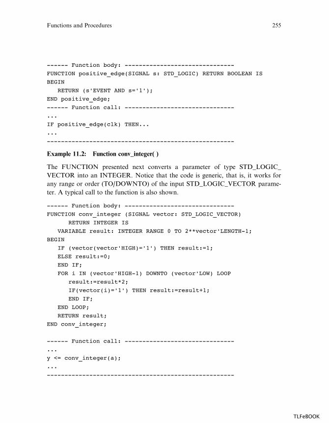
------ Function body: -------------------------------
FUNCTION positive_edge(SIGNAL s: STD_LOGIC) RETURN BOOLEAN IS
BEGIN
RETURN (s'EVENT AND s='1');
END positive_edge;
------ Function call: -------------------------------
...
IF positive_edge(clk) THEN...
...
-----------------------------------------------------
Example 11.2: Function conv_integer( )
The FUNCTION presented next converts a parameter of type STD_LOGIC_
VECTOR into an INTEGER. Notice that the code is generic, that is, it works for
any range or order (TO/DOWNTO) of the input STD_LOGIC_VECTOR parame-
ter. A typical call to the function is also shown.
------ Function body: -------------------------------
FUNCTION conv_integer (SIGNAL vector: STD_LOGIC_VECTOR)
RETURN INTEGER IS
VARIABLE result: INTEGER RANGE 0 TO 2**vector'LENGTH-1;
BEGIN
IF (vector(vector'HIGH)='1') THEN result:=1;
ELSE result:=0;
END IF;
FOR i IN (vector'HIGH-1) DOWNTO (vector'LOW) LOOP
result:=result*2;
IF(vector(i)='1') THEN result:=result+1;
END IF;
END LOOP;
RETURN result;
END conv_integer;
------ Function call: -------------------------------
...
y <= conv_integer(a);
...
-----------------------------------------------------
Functions and Procedures 255
TLFeBOOK
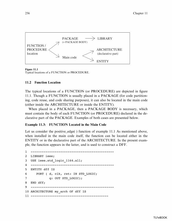
11.2 Function Location
The typical locations of a FUNCTION (or PROCEDURE) are depicted in figure
11.1. Though a FUNCTION is usually placed in a PACKAGE (for code partition-
ing, code reuse, and code sharing purposes), it can also be located in the main code
(either inside the ARCHITECTURE or inside the ENTITY).
When placed in a PACKAGE, then a PACKAGE BODY is necessary, which
must contain the body of each FUNCTION (or PROCEDURE) declared in the de-
clarative part of the PACKAGE. Examples of both cases are presented below.
Example 11.3: FUNCTION Located in the Main Code
Let us consider the positive_edge( ) function of example 11.1 As mentioned above,
when installed in the main code itself, the function can be located either in the
ENTITY or in the declarative part of the ARCHITECTURE. In the present exam-
ple, the function appears in the latter, and is used to construct a DFF.
1 ---------------------------------------------
2 LIBRARY ieee;
3 USE ieee.std_logic_1164.all;
4 ---------------------------------------------
5 ENTITY dff IS
6 PORT ( d, clk, rst: IN STD_LOGIC;
7 q: OUT STD_LOGIC);
8 END dff;
9 ---------------------------------------------
10 ARCHITECTURE my_arch OF dff IS
11 ------------------------------------------
PACKAGE LIBRARY(+ PACKAGE BODY)
FUNCTION / PROCEDURE ARCHITECTURE location (declarative part)
Main code ENTITY
Figure 11.1Typical locations of a FUNCTION or PROCEDURE.
256 Chapter 11
TLFeBOOK

12 FUNCTION positive_edge(SIGNAL s: STD_LOGIC)
13 RETURN BOOLEAN IS
14 BEGIN
15 RETURN s'EVENT AND s='1';
16 END positive_edge;
17 ------------------------------------------
18 BEGIN
19 PROCESS (clk, rst)
20 BEGIN
21 IF (rst='1') THEN q <= '0';
22 ELSIF positive_edge(clk) THEN q <= d;
23 END IF;
24 END PROCESS;
25 END my_arch;
26 ---------------------------------------------
Example 11.4: FUNCTION Located in a PACKAGE
This example is similar to example 11.3, with the only di¤erence being that the
FUNCTION located in a PACKAGE can now be reused and shared by other proj-
ects. Notice that, when placed in a PACKAGE, the function is indeed declared in the
PACKAGE, but described in the PACKAGE BODY.
Below two VHDL codes are presented, being one relative to the construction of
the FUNCTION / PACKAGE, while the other is an example where a call to the
FUNCTION is made. The two codes can be compiled as two separate files, or can be
compiled as a single file (saved as d¤.vhd, which is the ENTITY’s name). Notice the
inclusion of ‘‘USE work.my_package.all;’’ in the main code (line 4).
1 ------- Package: -----------------------------
2 LIBRARY ieee;
3 USE ieee.std_logic_1164.all;
4 ----------------------------------------------
5 PACKAGE my_package IS
6 FUNCTION positive_edge(SIGNAL s: STD_LOGIC) RETURN BOOLEAN;
7 END my_package;
8 ----------------------------------------------
9 PACKAGE BODY my_package IS
10 FUNCTION positive_edge(SIGNAL s: STD_LOGIC)
11 RETURN BOOLEAN IS
Functions and Procedures 257
TLFeBOOK
12 BEGIN
13 RETURN s'EVENT AND s='1';
14 END positive_edge;
15 END my_package;
16 ----------------------------------------------
1 ------ Main code: ----------------------------
2 LIBRARY ieee;
3 USE ieee.std_logic_1164.all;
4 USE work.my_package.all;
5 ----------------------------------------------
6 ENTITY dff IS
7 PORT ( d, clk, rst: IN STD_LOGIC;
8 q: OUT STD_LOGIC);
9 END dff;
10 ----------------------------------------------
11 ARCHITECTURE my_arch OF dff IS
12 BEGIN
13 PROCESS (clk, rst)
14 BEGIN
15 IF (rst='1') THEN q <= '0';
16 ELSIF positive_edge(clk) THEN q <= d;
17 END IF;
18 END PROCESS;
19 END my_arch;
20 ----------------------------------------------
Example 11.5: Function conv_integer( )
The conv_integer( ) function shown below was already seen in example 11.2; it con-
verts a STD_LOGIC_VECTOR value into an INTEGER value. Below, the function
was placed in a PACKAGE (plus PACKAGE BODY). A call to this function
appears in the main code that follows the function implementation.
1 --------- Package: ---------------------------
2 LIBRARY ieee;
3 USE ieee.std_logic_1164.all;
4 ----------------------------------------------
5 PACKAGE my_package IS
258 Chapter 11
TLFeBOOK

6 FUNCTION conv_integer (SIGNAL vector: STD_LOGIC_VECTOR)
7 RETURN INTEGER;
8 END my_package;
9 ----------------------------------------------
10 PACKAGE BODY my_package IS
11 FUNCTION conv_integer (SIGNAL vector: STD_LOGIC_VECTOR)
12 RETURN INTEGER IS
13 VARIABLE result: INTEGER RANGE 0 TO 2**vector'LENGTH-1;
14 BEGIN
15 IF (vector(vector'HIGH)='1') THEN result:=1;
16 ELSE result:=0;
17 END IF;
18 FOR i IN (vector'HIGH-1) DOWNTO (vector'LOW) LOOP
19 result:=result*2;
20 IF(vector(i)='1') THEN result:=result+1;
21 END IF;
22 END LOOP;
23 RETURN result;
24 END conv_integer;
25 END my_package;
26 ----------------------------------------------
1 -------- Main code: --------------------------
2 LIBRARY ieee;
3 USE ieee.std_logic_1164.all;
4 USE work.my_package.all;
5 ----------------------------------------------
6 ENTITY conv_int2 IS
7 PORT ( a: IN STD_LOGIC_VECTOR(0 TO 3);
8 y: OUT INTEGER RANGE 0 TO 15);
9 END conv_int2;
10 ----------------------------------------------
11 ARCHITECTURE my_arch OF conv_int2 IS
12 BEGIN
13 y <= conv_integer(a);
14 END my_arch;
15 ----------------------------------------------
Functions and Procedures 259
TLFeBOOK
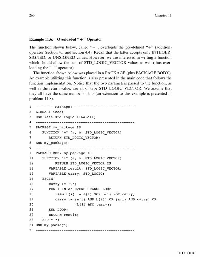
Example 11.6: Overloaded ‘‘B’’ Operator
The function shown below, called ‘‘þ’’, overloads the pre-defined ‘‘þ’’ (addition)
operator (section 4.1 and section 4.4). Recall that the latter accepts only INTEGER,
SIGNED, or UNSIGNED values. However, we are interested in writing a function
which should allow the sum of STD_LOGIC_VECTOR values as well (thus over-
loading the ‘‘þ’’ operator).
The function shown below was placed in a PACKAGE (plus PACKAGE BODY).
An example utilizing this function is also presented in the main code that follows the
function implementation. Notice that the two parameters passed to the function, as
well as the return value, are all of type STD_LOGIC_VECTOR. We assume that
they all have the same number of bits (an extension to this example is presented in
problem 11.8).
1 -------- Package: ----------------------------
2 LIBRARY ieee;
3 USE ieee.std_logic_1164.all;
4 ----------------------------------------------
5 PACKAGE my_package IS
6 FUNCTION "+" (a, b: STD_LOGIC_VECTOR)
7 RETURN STD_LOGIC_VECTOR;
8 END my_package;
9 ----------------------------------------------
10 PACKAGE BODY my_package IS
11 FUNCTION "+" (a, b: STD_LOGIC_VECTOR)
12 RETURN STD_LOGIC_VECTOR IS
13 VARIABLE result: STD_LOGIC_VECTOR;
14 VARIABLE carry: STD_LOGIC;
15 BEGIN
16 carry := '0';
17 FOR i IN a'REVERSE_RANGE LOOP
18 result(i) := a(i) XOR b(i) XOR carry;
19 carry := (a(i) AND b(i)) OR (a(i) AND carry) OR
20 (b(i) AND carry);
21 END LOOP;
22 RETURN result;
23 END "+";
24 END my_package;
25 ----------------------------------------------
260 Chapter 11
TLFeBOOK

1 --------- Main code: -------------------------
2 LIBRARY ieee;
3 USE ieee.std_logic_1164.all;
4 USE work.my_package.all;
5 ----------------------------------------------
6 ENTITY add_bit IS
7 PORT ( a: IN STD_LOGIC_VECTOR(3 DOWNTO 0);
8 y: OUT STD_LOGIC_VECTOR(3 DOWNTO 0));
9 END add_bit;
10 ----------------------------------------------
11 ARCHITECTURE my_arch OF add_bit IS
12 CONSTANT b: STD_LOGIC_VECTOR(3 DOWNTO 0) := "0011";
13 CONSTANT c: STD_LOGIC_VECTOR(3 DOWNTO 0) := "0110";
14 BEGIN
15 y <= a + b + c; -- overloaded "+" operator
16 END my_arch;
17 ----------------------------------------------
Simulation results, for 4-bit numbers, are presented in figure 11.2. We have entered
b ¼ 3 and c ¼ 6 as two constants, which are added to the input signal a. The
expected results is then y ¼ aþ 9.
Example 11.7: Arithmetic Shift Function
The function shown below arithmetically shifts a STD_LOGIC_VECTOR value to
the left. Two arguments are passed to the function: arg1 and arg2. The first is the
vector to be shifted, while the second specifies the amount of shift. Notice that the
function (lines 13–26) is totally generic; that is, it works for any size (number of bits)
or order (TO/DOWNTO) of the input vector. In this example, the function was
located in the main code instead of in a package.
Figure 11.2Simulation results of example 11.6.
Functions and Procedures 261
TLFeBOOK
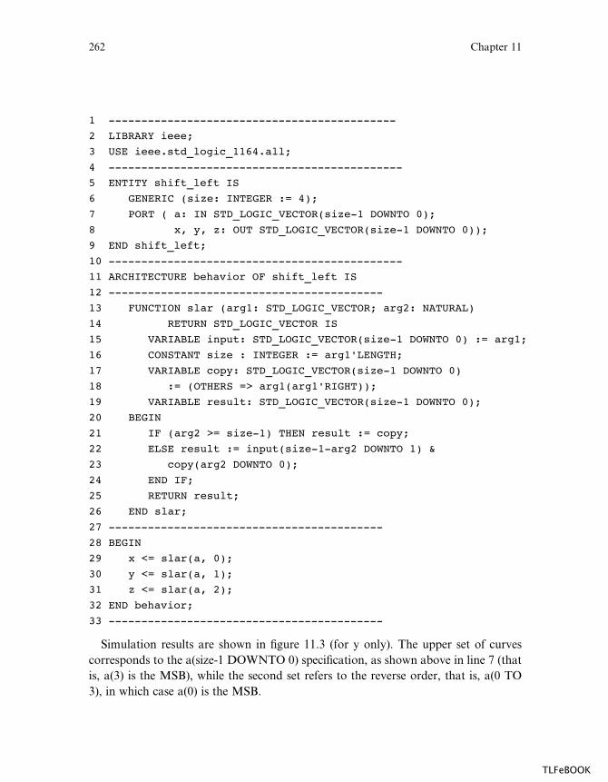
1 --------------------------------------------
2 LIBRARY ieee;
3 USE ieee.std_logic_1164.all;
4 ---------------------------------------------
5 ENTITY shift_left IS
6 GENERIC (size: INTEGER := 4);
7 PORT ( a: IN STD_LOGIC_VECTOR(size-1 DOWNTO 0);
8 x, y, z: OUT STD_LOGIC_VECTOR(size-1 DOWNTO 0));
9 END shift_left;
10 ---------------------------------------------
11 ARCHITECTURE behavior OF shift_left IS
12 ------------------------------------------
13 FUNCTION slar (arg1: STD_LOGIC_VECTOR; arg2: NATURAL)
14 RETURN STD_LOGIC_VECTOR IS
15 VARIABLE input: STD_LOGIC_VECTOR(size-1 DOWNTO 0) := arg1;
16 CONSTANT size : INTEGER := arg1'LENGTH;
17 VARIABLE copy: STD_LOGIC_VECTOR(size-1 DOWNTO 0)
18 := (OTHERS => arg1(arg1'RIGHT));
19 VARIABLE result: STD_LOGIC_VECTOR(size-1 DOWNTO 0);
20 BEGIN
21 IF (arg2 >= size-1) THEN result := copy;
22 ELSE result := input(size-1-arg2 DOWNTO 1) &
23 copy(arg2 DOWNTO 0);
24 END IF;
25 RETURN result;
26 END slar;
27 ------------------------------------------
28 BEGIN
29 x <= slar(a, 0);
30 y <= slar(a, 1);
31 z <= slar(a, 2);
32 END behavior;
33 ------------------------------------------
Simulation results are shown in figure 11.3 (for y only). The upper set of curves
corresponds to the a(size-1 DOWNTO 0) specification, as shown above in line 7 (that
is, a(3) is the MSB), while the second set refers to the reverse order, that is, a(0 TO
3), in which case a(0) is the MSB.
262 Chapter 11
TLFeBOOK
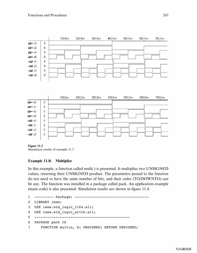
Example 11.8: Multiplier
In this example, a function called mult( ) is presented. It multiplies two UNSIGNED
values, returning their UNSIGNED product. The parameters passed to the function
do not need to have the same number of bits, and their order (TO/DOWNTO) can
be any. The function was installed in a package called pack. An application example
(main code) is also presented. Simulation results are shown in figure 11.4.
1 --------- Package: -----------------------------------
2 LIBRARY ieee;
3 USE ieee.std_logic_1164.all;
4 USE ieee.std_logic_arith.all;
5 ---------------------------------------------
6 PACKAGE pack IS
7 FUNCTION mult(a, b: UNSIGNED) RETURN UNSIGNED;
Figure 11.3Simulation results of example 11.7.
Functions and Procedures 263
TLFeBOOK
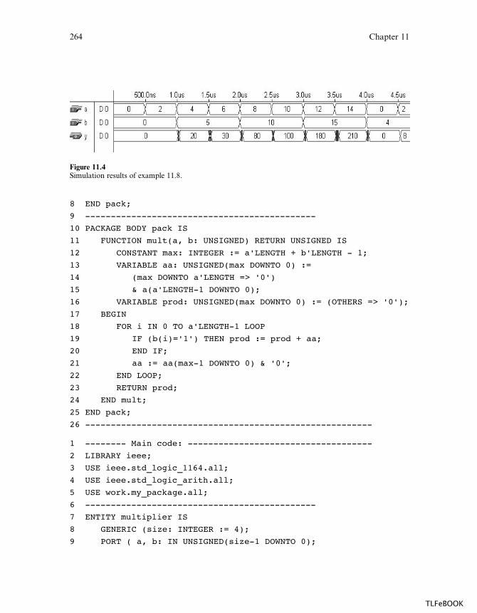
8 END pack;
9 ---------------------------------------------
10 PACKAGE BODY pack IS
11 FUNCTION mult(a, b: UNSIGNED) RETURN UNSIGNED IS
12 CONSTANT max: INTEGER := a'LENGTH + b'LENGTH - 1;
13 VARIABLE aa: UNSIGNED(max DOWNTO 0) :=
14 (max DOWNTO a'LENGTH => '0')
15 & a(a'LENGTH-1 DOWNTO 0);
16 VARIABLE prod: UNSIGNED(max DOWNTO 0) := (OTHERS => '0');
17 BEGIN
18 FOR i IN 0 TO a'LENGTH-1 LOOP
19 IF (b(i)='1') THEN prod := prod + aa;
20 END IF;
21 aa := aa(max-1 DOWNTO 0) & '0';
22 END LOOP;
23 RETURN prod;
24 END mult;
25 END pack;
26 --------------------------------------------------------
1 -------- Main code: ------------------------------------
2 LIBRARY ieee;
3 USE ieee.std_logic_1164.all;
4 USE ieee.std_logic_arith.all;
5 USE work.my_package.all;
6 ---------------------------------------------
7 ENTITY multiplier IS
8 GENERIC (size: INTEGER := 4);
9 PORT ( a, b: IN UNSIGNED(size-1 DOWNTO 0);
Figure 11.4Simulation results of example 11.8.
264 Chapter 11
TLFeBOOK
10 y: OUT UNSIGNED(2*size-1 DOWNTO 0));
11 END multiplier;
12 ---------------------------------------------
13 ARCHITECTURE behavior OF multiplier IS
14 BEGIN
15 y <= mult(a,b);
16 END behavior;
17 ---------------------------------------------------------
11.3 PROCEDURE
A PROCEDURE is very similar to a FUNCTION and has the same basic purposes.
However, a procedure can return more than one value.
Like a FUNCTION, two parts are necessary to construct and use a PROCE-
DURE: the procedure itself (procedure body) and a procedure call.
Procedure Body
PROCEDURE procedure_name [<parameter list>] IS[declarations]
BEGIN(sequential statements)
END procedure_name;
In the syntax above, <parameter list> specifies the procedure’s input and output
parameters; that is:
3parameter list4 ¼ [CONSTANT] constant_name: mode type;
3parameter list4 ¼ SIGNAL signal_name: mode type; or
3parameter list4 ¼ VARIABLE variable_name: mode type;
A PROCEDURE can have any number of IN, OUT, or INOUT parameters,
which can be SIGNALS, VARIABLES, or CONSTANTS. For input signals (mode
IN), the default is CONSTANT, whereas for output signals (mode OUT or INOUT)
the default is VARIABLE.
As seen before, WAIT, SIGNAL declarations, and COMPONENTS are not syn-
thesizable when used in a FUNCTION. The same is true for a PROCEDURE, with
Functions and Procedures 265
TLFeBOOK
the exception that a SIGNAL can be declared, but then the PROCEDURE must be
declared in a PROCESS. Moreover, besides WAIT, any other edge detection is also
not synthesizable with a PROCEDURE (that is, contrary to a function, a synthesiz-
able procedure should not infer registers).
In section 11.5, a summary comparing FUNCTIONS and PROCEDURES will be
presented.
Example: The PROCEDURE below has three inputs, a, b, and c (mode IN). a is a
CONSTANT of type BIT, while b and c are SIGNALS, also of type BIT. Notice
that the word CONSTANT can be omitted for input parameters, for it is the default
object (recall, however, that for outputs the default object is VARIABLE). There are
also two return signals, x (mode OUT, type BIT_VECTOR) and y (mode INOUT,
type INTEGER).
PROCEDURE my_procedure ( a: IN BIT; SIGNAL b, c: IN BIT;
SIGNAL x: OUT BIT_VECTOR(7 DOWNTO 0);
SIGNAL y: INOUT INTEGER RANGE 0 TO 99) IS
BEGIN
...
END my_procedure;
Procedure Call
Contrary to a FUNCTION, which is called as part of an expression, a PROCE-
DURE call is a statement on its own. It can appear by itself or associated to a
statement (either concurrent or sequential).
Examples of procedure calls:
compute_min_max(in1, in2, 1n3, out1, out2);
-- statement by itself
divide(dividend, divisor, quotient, remainder);
-- statement by itself
IF (a>b) THEN compute_min_max(in1, in2, 1n3, out1, out2);
-- procedure call associated to another statement
11.4 Procedure Location
The typical locations of a PROCEDURE are the same as those of a FUNCTION
(see figure 11.1). Again, though it is usually placed in a PACKAGE (for code parti-
266 Chapter 11
TLFeBOOK
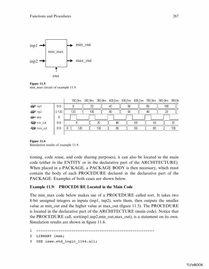
tioning, code reuse, and code sharing purposes), it can also be located in the main
code (either in the ENTITY or in the declarative part of the ARCHITECTURE).
When placed in a PACKAGE, a PACKAGE BODY is then necessary, which must
contain the body of each PROCEDURE declared in the declarative part of the
PACKAGE. Examples of both cases are shown below.
Example 11.9: PROCEDURE Located in the Main Code
The min_max code below makes use of a PROCEDURE called sort. It takes two
8-bit unsigned integers as inputs (inp1, inp2), sorts them, then outputs the smaller
value at min_out and the higher value at max_out (figure 11.5). The PROCEDURE
is located in the declarative part of the ARCHITECTURE (main code). Notice that
the PROCEDURE call, sort(inp1,inp2,min_out,max_out), is a statement on its own.
Simulation results are shown in figure 11.6.
1 ------------------------------------------------------
2 LIBRARY ieee;
3 USE ieee.std_logic_1164.all;
inp1
inp2
ena
min_max
min_out
max_out
Figure 11.5min_max circuit of example 11.9.
Figure 11.6Simulation results of example 11.9.
Functions and Procedures 267
TLFeBOOK
4 ------------------------------------------------------
5 ENTITY min_max IS
6 GENERIC (limit : INTEGER := 255);
7 PORT ( ena: IN BIT;
8 inp1, inp2: IN INTEGER RANGE 0 TO limit;
9 min_out, max_out: OUT INTEGER RANGE 0 TO limit);
10 END min_max;
11 ------------------------------------------------------
12 ARCHITECTURE my_architecture OF min_max IS
13 --------------------------
14 PROCEDURE sort (SIGNAL in1, in2: IN INTEGER RANGE 0 TO limit;
15 SIGNAL min, max: OUT INTEGER RANGE 0 TO limit) IS
16 BEGIN
17 IF (in1 > in2) THEN
18 max <= in1;
19 min <= in2;
20 ELSE
21 max <= in2;
22 min <= in1;
23 END IF;
24 END sort;
25 --------------------------
26 BEGIN
27 PROCESS (ena)
28 BEGIN
29 IF (ena='1') THEN sort (inp1, inp2, min_out, max_out);
30 END IF;
31 END PROCESS;
32 END my_architecture;
33 ------------------------------------------------------
Example 11.10: PROCEDURE Located in a PACKAGE
This example is similar to example 11.9, with the only di¤erence being that now the
PROCEDURE (called sort) is placed in a PACKAGE (called my_package). Thus
the PROCEDURE can now be reused and shared with other designs. The code
below can be compiled as two separate files, or can be compiled as a single file (called
min_max.vhd, which is the ENTITY’s name).
268 Chapter 11
TLFeBOOK

1 ------------ Package: ---------------------------
2 LIBRARY ieee;
3 USE ieee.std_logic_1164.all;
4 -------------------------------------
5 PACKAGE my_package IS
6 CONSTANT limit: INTEGER := 255;
7 PROCEDURE sort (SIGNAL in1, in2: IN INTEGER RANGE 0 TO limit;
8 SIGNAL min, max: OUT INTEGER RANGE 0 TO limit);
9 END my_package;
10 -------------------------------------
11 PACKAGE BODY my_package IS
12 PROCEDURE sort (SIGNAL in1, in2: IN INTEGER RANGE 0 TO limit;
13 SIGNAL min, max: OUT INTEGER RANGE 0 TO limit) IS
14 BEGIN
15 IF (in1 > in2) THEN
16 max <= in1;
17 min <= in2;
18 ELSE
19 max <= in2;
20 min <= in1;
21 END IF;
22 END sort;
23 END my_package;
24 -------------------------------------------------
1 --------- Main code: ----------------------------
2 LIBRARY ieee;
3 USE ieee.std_logic_1164.all;
4 USE work.my_package.all;
5 -------------------------------------
6 ENTITY min_max IS
7 GENERIC (limit: INTEGER := 255);
8 PORT ( ena: IN BIT;
9 inp1, inp2: IN INTEGER RANGE 0 TO limit;
10 min_out, max_out: OUT INTEGER RANGE 0 TO limit);
11 END min_max;
12 -------------------------------------
Functions and Procedures 269
TLFeBOOK
13 ARCHITECTURE my_architecture OF min_max IS
14 BEGIN
15 PROCESS (ena)
16 BEGIN
17 IF (ena='1') THEN sort (inp1, inp2, min_out, max_out);
18 END IF;
19 END PROCESS;
20 END my_architecture;
21 ----------------------------------------------
The simulation results are obviously the same as those of example 11.9 (figure
11.6).
11.5 FUNCTION versus PROCEDURE Summary
� A FUNCTION has zero or more input parameters and a single return value. The
input parameters can only be CONSTANTS (default) or SIGNALS (VARIABLES
are not allowed).
� A PROCEDURE can have any number of IN, OUT, and INOUT parameters,
which can be SIGNALS, VARIABLES, or CONSTANTS. For input parameters
(mode IN) the default is CONSTANT, whereas for output parameters (mode OUT
or INOUT) the default is VARIABLE.
� A FUNCTION is called as part of an expression, while a PROCEDURE is a
statement on its own.
� In both, WAIT and COMPONENTS are not synthesizable.
� The possible locations of FUNCTIONS and PROCEDURES are the same (figure
11.1). Though they are usually placed in PACKAGES (for code partitioning, code
sharing, and code reuse purposes), they can also be located in the main code (either
inside the ARCHITECTURE or inside the ENTITY). When placed in a PACK-
AGE, then a PACKAGE BODY is necessary, which should contain the body of
each FUNCTION and/or PROCEDURE declared in the PACKAGE.
11.6 ASSERT
ASSERT is a non-synthesizable statement whose purpose is to write out messages
(on the screen, for example) when problems are found during simulation. Depending
270 Chapter 11
TLFeBOOK
on the severity of the problem, the simulator is instructed to halt. Its syntax is the
following:
ASSERT condition[REPORT "message"][SEVERITY severity_level];
The severity level can be: Note, Warning, Error (default), or Failure. The message
is written when the condition is FALSE.
Example: Say that we have written a function to add two binary numbers (like in
example 11.6), where it was assumed that the input parameters must have the same
number of bits. In order to check such an assumption, the following ASSERT state-
ment could be included in the function body:
ASSERT a'LENGTH = b'LENGTH
REPORT "Error: vectors do not have same length!"
SEVERITY failure;
Again, ASSERT does not generate hardware. Synthesis tools will simply ignore it
or give a warning.
11.7 Problems
The purpose of the problems proposed in this section is to reinforce the main aspects
related to the construction and use of subprograms (FUNCTIONS and PROCE-
DURES).
Problem 11.1: Conversion to std_logic_vector
Write a function capable of converting an INTEGER to a STD_LOGIC_VECTOR
value. Call it conv_std_logic( ). Then write an application example, containing a call
to your function, in order to test it. Construct two solutions: one with the function in
the main code itself, and one with it in a package.
Problem 11.2: Overloaded ‘‘not’’ Operator
The NOT operator allows the inversion of binary values. For example, if x ¼ ‘‘1000’’
is a STD_LOGIC_VECTOR value, then NOT x could be used, producing ‘‘0111’’.
Functions and Procedures 271
TLFeBOOK
However, if x had been declared as an INTEGER, such operation would not be
allowed. Write a ‘‘not’’ function capable of inverting integers. (Suggestion: See sec-
tion 4.4 and example 11.6.)
Problem 11.3: Logic Shift of std_logic_vector
The pre-defined shift operators (specified in VHDL93, section 4.1) work only with
type BIT_VECTOR. Write a function capable of logically shifting a STD_LOGC_
VECTOR signal to the left by a specified amount. Two arguments must be passed to
the function: the value to be shifted (STD_LOGIC_VECTOR), plus a NATURAL
value specifying the amount of shift. Place your function in a package. Then write an
application with a call to your function in order to test it (suggestion: review example
11.7).
Problem 11.4: Logic Shift of an Integer
This problem is an extension of problem 11.3. Write a function capable of shifting an
INTEGER value to the left by an specified amount. Place your function in a pack-
age. Then write an application with a call to your function in order to test it.
Problem 11.5: Signed Multiplier
Write a function similar to that of example 11.8. However, it should now operate
with SIGNED input and output values.
Problem 11.6: Two-digit Counter with SSD Output
In example 6.7, a progressive 2-digit decimal counter (0 ! 99 ! 0), with external
asynchronous reset plus binary-coded decimal (BCD) to seven-segment display
(SSD) conversion, was designed. In it, a routine to convert a signal from BCD to
SSD format was used twice. This kind of repetition can be avoided with a FUNC-
TION. Write a function (call it bcd_to_ssd) capable of making such a conversion
and place it in a PACKAGE. Then redo the design of example 6.7, using a call to
your function whenever such conversion is needed. Then synthesize and test your
solution.
Problem 11.7: Statistical Procedure
Write a PROCEDURE that receives eight signed values and returns their average,
the largest value, and the lowest value. Call the return values ave, max, and min.
Place your procedure in a package. Then write an application with a call to it in
order to test its functionality.
272 Chapter 11
TLFeBOOK
Problem 11.8: Overloaded ‘‘B’’ Operator
In example 11.6, a function that overloads the ‘‘þ’’ (addition) operator was pre-
sented. Its purpose was to allow the direct addition of STD_LOGIC_VECTOR
values. In that example, the return parameter had the same number of bits as the two
input parameters. Write a similar function, but with the return vector having one
extra bit corresponding to the carry out bit such that overflow can then be easily
detected.
Functions and Procedures 273
TLFeBOOK

TLFeBOOK
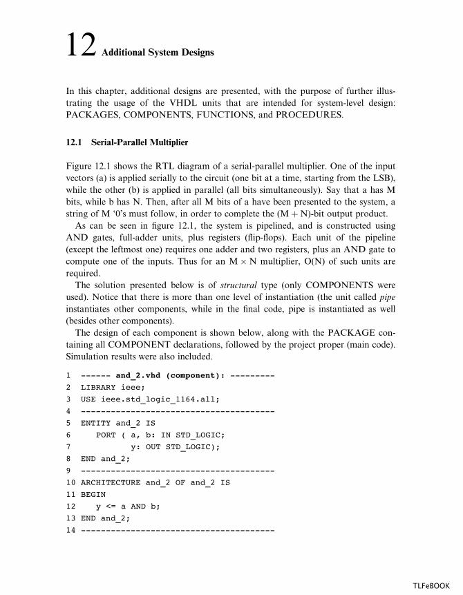
12 Additional System Designs
In this chapter, additional designs are presented, with the purpose of further illus-
trating the usage of the VHDL units that are intended for system-level design:
PACKAGES, COMPONENTS, FUNCTIONS, and PROCEDURES.
12.1 Serial-Parallel Multiplier
Figure 12.1 shows the RTL diagram of a serial-parallel multiplier. One of the input
vectors (a) is applied serially to the circuit (one bit at a time, starting from the LSB),
while the other (b) is applied in parallel (all bits simultaneously). Say that a has M
bits, while b has N. Then, after all M bits of a have been presented to the system, a
string of M ‘0’s must follow, in order to complete the (MþN)-bit output product.
As can be seen in figure 12.1, the system is pipelined, and is constructed using
AND gates, full-adder units, plus registers (flip-flops). Each unit of the pipeline
(except the leftmost one) requires one adder and two registers, plus an AND gate to
compute one of the inputs. Thus for an M�N multiplier, O(N) of such units are
required.
The solution presented below is of structural type (only COMPONENTS were
used). Notice that there is more than one level of instantiation (the unit called pipe
instantiates other components, while in the final code, pipe is instantiated as well
(besides other components).
The design of each component is shown below, along with the PACKAGE con-
taining all COMPONENT declarations, followed by the project proper (main code).
Simulation results were also included.
1 ------ and_2.vhd (component): ---------
2 LIBRARY ieee;
3 USE ieee.std_logic_1164.all;
4 ---------------------------------------
5 ENTITY and_2 IS
6 PORT ( a, b: IN STD_LOGIC;
7 y: OUT STD_LOGIC);
8 END and_2;
9 ---------------------------------------
10 ARCHITECTURE and_2 OF and_2 IS
11 BEGIN
12 y <= a AND b;
13 END and_2;
14 ---------------------------------------
TLFeBOOK
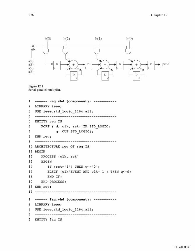
1 ------ reg.vhd (component): -----------
2 LIBRARY ieee;
3 USE ieee.std_logic_1164.all;
4 ---------------------------------------
5 ENTITY reg IS
6 PORT ( d, clk, rst: IN STD_LOGIC;
7 q: OUT STD_LOGIC);
8 END reg;
9 ---------------------------------------
10 ARCHITECTURE reg OF reg IS
11 BEGIN
12 PROCESS (clk, rst)
13 BEGIN
14 IF (rst='1') THEN q<='0';
15 ELSIF (clk'EVENT AND clk='1') THEN q<=d;
16 END IF;
17 END PROCESS;
18 END reg;
19 ---------------------------------------
1 ------ fau.vhd (component): -----------
2 LIBRARY ieee;
3 USE ieee.std_logic_1164.all;
4 ---------------------------------------
5 ENTITY fau IS
+
D
D +
D
+
D
b(3) b(2) b(1) b(0)
a(0)a(1)a(2)a(3)
a
prodD D D
Figure 12.1Serial-parallel multiplier.
276 Chapter 12
TLFeBOOK
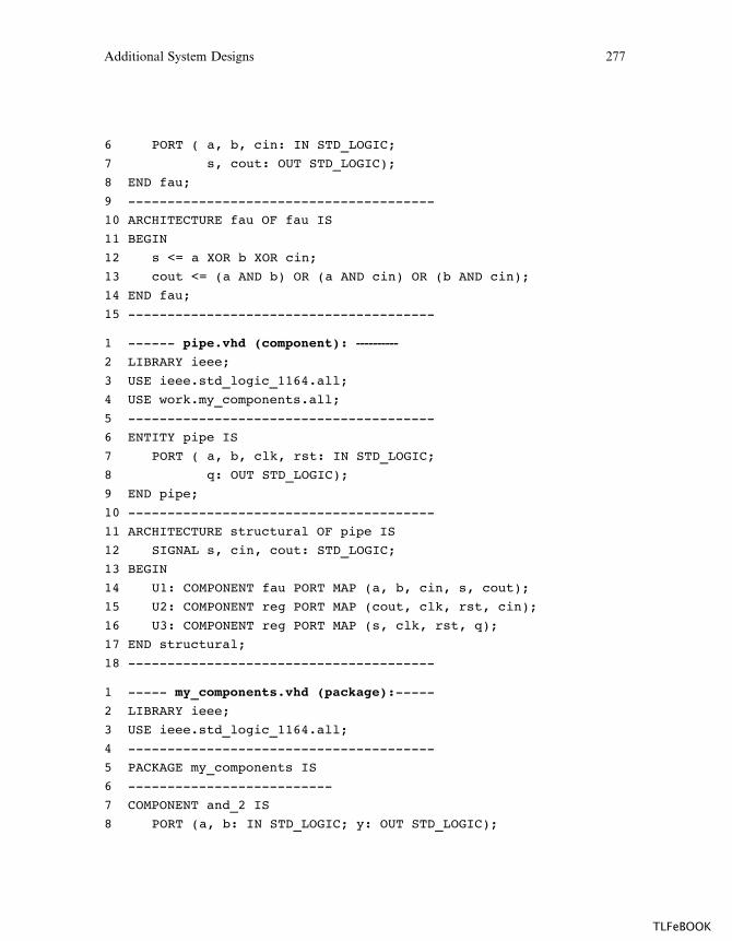
6 PORT ( a, b, cin: IN STD_LOGIC;
7 s, cout: OUT STD_LOGIC);
8 END fau;
9 ---------------------------------------
10 ARCHITECTURE fau OF fau IS
11 BEGIN
12 s <= a XOR b XOR cin;
13 cout <= (a AND b) OR (a AND cin) OR (b AND cin);
14 END fau;
15 ---------------------------------------
1 ------ pipe.vhd (component): ----------
2 LIBRARY ieee;
3 USE ieee.std_logic_1164.all;
4 USE work.my_components.all;
5 ---------------------------------------
6 ENTITY pipe IS
7 PORT ( a, b, clk, rst: IN STD_LOGIC;
8 q: OUT STD_LOGIC);
9 END pipe;
10 ---------------------------------------
11 ARCHITECTURE structural OF pipe IS
12 SIGNAL s, cin, cout: STD_LOGIC;
13 BEGIN
14 U1: COMPONENT fau PORT MAP (a, b, cin, s, cout);
15 U2: COMPONENT reg PORT MAP (cout, clk, rst, cin);
16 U3: COMPONENT reg PORT MAP (s, clk, rst, q);
17 END structural;
18 ---------------------------------------
1 ----- my_components.vhd (package):-----
2 LIBRARY ieee;
3 USE ieee.std_logic_1164.all;
4 ---------------------------------------
5 PACKAGE my_components IS
6 --------------------------
7 COMPONENT and_2 IS
8 PORT (a, b: IN STD_LOGIC; y: OUT STD_LOGIC);
Additional System Designs 277
TLFeBOOK
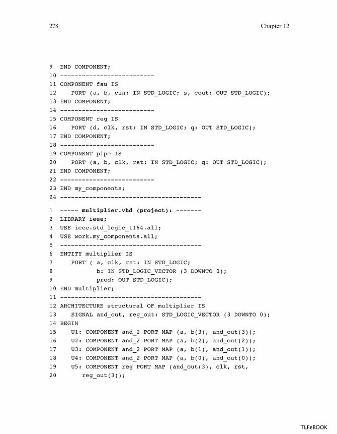
9 END COMPONENT;
10 --------------------------
11 COMPONENT fau IS
12 PORT (a, b, cin: IN STD_LOGIC; s, cout: OUT STD_LOGIC);
13 END COMPONENT;
14 --------------------------
15 COMPONENT reg IS
16 PORT (d, clk, rst: IN STD_LOGIC; q: OUT STD_LOGIC);
17 END COMPONENT;
18 --------------------------
19 COMPONENT pipe IS
20 PORT (a, b, clk, rst: IN STD_LOGIC; q: OUT STD_LOGIC);
21 END COMPONENT;
22 --------------------------
23 END my_components;
24 ---------------------------------------
1 ----- multiplier.vhd (project): -------
2 LIBRARY ieee;
3 USE ieee.std_logic_1164.all;
4 USE work.my_components.all;
5 ---------------------------------------
6 ENTITY multiplier IS
7 PORT ( a, clk, rst: IN STD_LOGIC;
8 b: IN STD_LOGIC_VECTOR (3 DOWNTO 0);
9 prod: OUT STD_LOGIC);
10 END multiplier;
11 ---------------------------------------
12 ARCHITECTURE structural OF multiplier IS
13 SIGNAL and_out, reg_out: STD_LOGIC_VECTOR (3 DOWNTO 0);
14 BEGIN
15 U1: COMPONENT and_2 PORT MAP (a, b(3), and_out(3));
16 U2: COMPONENT and_2 PORT MAP (a, b(2), and_out(2));
17 U3: COMPONENT and_2 PORT MAP (a, b(1), and_out(1));
18 U4: COMPONENT and_2 PORT MAP (a, b(0), and_out(0));
19 U5: COMPONENT reg PORT MAP (and_out(3), clk, rst,
20 reg_out(3));
278 Chapter 12
TLFeBOOK
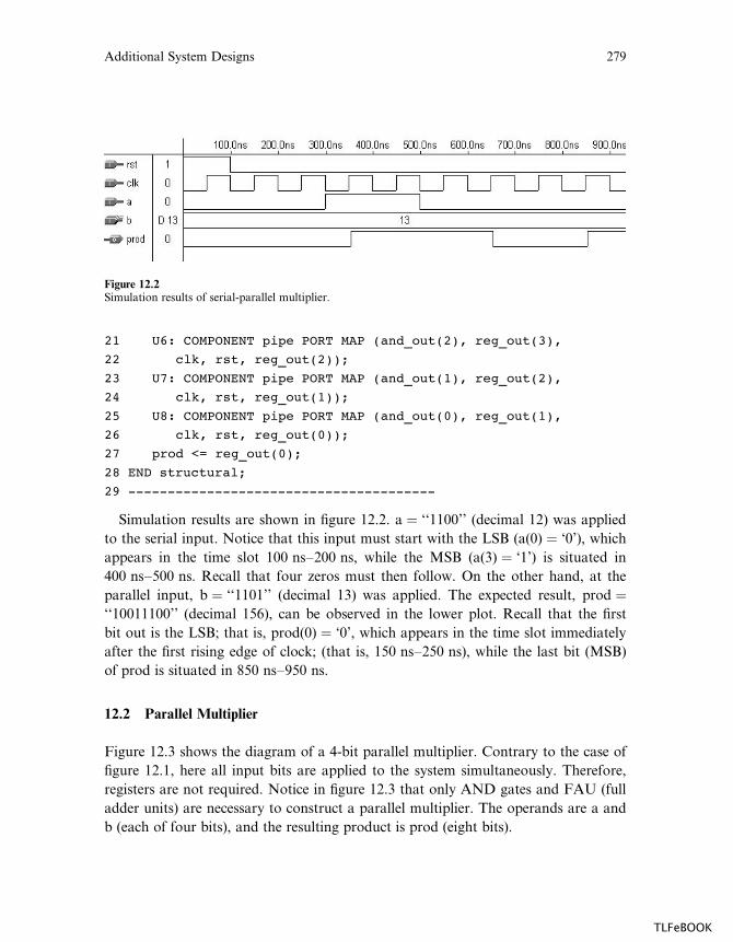
21 U6: COMPONENT pipe PORT MAP (and_out(2), reg_out(3),
22 clk, rst, reg_out(2));
23 U7: COMPONENT pipe PORT MAP (and_out(1), reg_out(2),
24 clk, rst, reg_out(1));
25 U8: COMPONENT pipe PORT MAP (and_out(0), reg_out(1),
26 clk, rst, reg_out(0));
27 prod <= reg_out(0);
28 END structural;
29 ---------------------------------------
Simulation results are shown in figure 12.2. a ¼ ‘‘1100’’ (decimal 12) was applied
to the serial input. Notice that this input must start with the LSB (a(0) ¼ ‘0’), which
appears in the time slot 100 ns–200 ns, while the MSB (a(3) ¼ ‘1’) is situated in
400 ns–500 ns. Recall that four zeros must then follow. On the other hand, at the
parallel input, b ¼ ‘‘1101’’ (decimal 13) was applied. The expected result, prod ¼‘‘10011100’’ (decimal 156), can be observed in the lower plot. Recall that the first
bit out is the LSB; that is, prod(0) ¼ ‘0’, which appears in the time slot immediately
after the first rising edge of clock; (that is, 150 ns–250 ns), while the last bit (MSB)
of prod is situated in 850 ns–950 ns.
12.2 Parallel Multiplier
Figure 12.3 shows the diagram of a 4-bit parallel multiplier. Contrary to the case of
figure 12.1, here all input bits are applied to the system simultaneously. Therefore,
registers are not required. Notice in figure 12.3 that only AND gates and FAU (full
adder units) are necessary to construct a parallel multiplier. The operands are a and
b (each of four bits), and the resulting product is prod (eight bits).
Figure 12.2Simulation results of serial-parallel multiplier.
Additional System Designs 279
TLFeBOOK
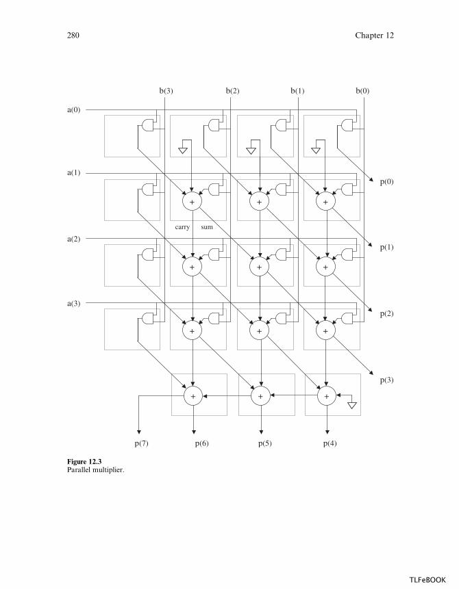
carry sum
b(3) b(2) b(1) b(0)
+ + +
+
+
+
+ +
+ +
+
p(7) p(6) p(5) p(4)
p(0)
p(1)
p(2)
p(3)
a(0)
a(1)
a(2)
a(3)
+
Figure 12.3Parallel multiplier.
280 Chapter 12
TLFeBOOK
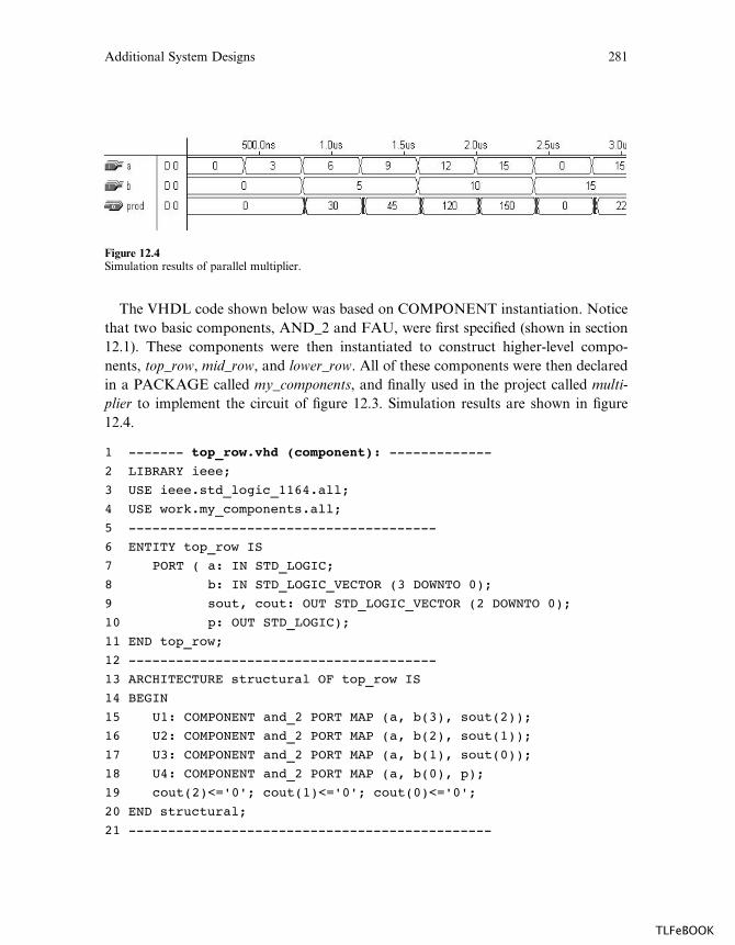
The VHDL code shown below was based on COMPONENT instantiation. Notice
that two basic components, AND_2 and FAU, were first specified (shown in section
12.1). These components were then instantiated to construct higher-level compo-
nents, top_row, mid_row, and lower_row. All of these components were then declared
in a PACKAGE called my_components, and finally used in the project called multi-
plier to implement the circuit of figure 12.3. Simulation results are shown in figure
12.4.
1 ------- top_row.vhd (component): -------------
2 LIBRARY ieee;
3 USE ieee.std_logic_1164.all;
4 USE work.my_components.all;
5 ---------------------------------------
6 ENTITY top_row IS
7 PORT ( a: IN STD_LOGIC;
8 b: IN STD_LOGIC_VECTOR (3 DOWNTO 0);
9 sout, cout: OUT STD_LOGIC_VECTOR (2 DOWNTO 0);
10 p: OUT STD_LOGIC);
11 END top_row;
12 ---------------------------------------
13 ARCHITECTURE structural OF top_row IS
14 BEGIN
15 U1: COMPONENT and_2 PORT MAP (a, b(3), sout(2));
16 U2: COMPONENT and_2 PORT MAP (a, b(2), sout(1));
17 U3: COMPONENT and_2 PORT MAP (a, b(1), sout(0));
18 U4: COMPONENT and_2 PORT MAP (a, b(0), p);
19 cout(2)<='0'; cout(1)<='0'; cout(0)<='0';
20 END structural;
21 ----------------------------------------------
Figure 12.4Simulation results of parallel multiplier.
Additional System Designs 281
TLFeBOOK

1 ------- mid_row.vhd (component): -------------
2 LIBRARY ieee;
3 USE ieee.std_logic_1164.all;
4 USE work.my_components.all;
5 ---------------------------------------
6 ENTITY mid_row IS
7 PORT ( a: IN STD_LOGIC;
8 b: IN STD_LOGIC_VECTOR (3 DOWNTO 0);
9 sin, cin: IN STD_LOGIC_VECTOR (2 DOWNTO 0);
10 sout, cout: OUT STD_LOGIC_VECTOR (2 DOWNTO 0);
11 p: OUT STD_LOGIC);
12 END mid_row;
13 ---------------------------------------
14 ARCHITECTURE structural OF mid_row IS
15 SIGNAL and_out: STD_LOGIC_VECTOR (2 DOWNTO 0);
16 BEGIN
17 U1: COMPONENT and_2 PORT MAP (a, b(3), sout(2));
18 U2: COMPONENT and_2 PORT MAP (a, b(2), and_out(2));
19 U3: COMPONENT and_2 PORT MAP (a, b(1), and_out(1));
20 U4: COMPONENT and_2 PORT MAP (a, b(0), and_out(0));
21 U5: COMPONENT fau PORT MAP (sin(2), cin(2), and_out(2),
22 sout(1), cout(2));
23 U6: COMPONENT fau PORT MAP (sin(1), cin(1), and_out(1),
24 sout(0), cout(1));
25 U7: COMPONENT fau PORT MAP (sin(0), cin(0), and_out(0),
26 p, cout(0));
27 END structural;
28 ----------------------------------------------
1 ------- lower_row.vhd (component): -----------
2 LIBRARY ieee;
3 USE ieee.std_logic_1164.all;
4 USE work.my_components.all;
5 ---------------------------------------
6 ENTITY lower_row IS
7 PORT ( sin, cin: IN STD_LOGIC_VECTOR (2 DOWNTO 0);
8 p: OUT STD_LOGIC_VECTOR (3 DOWNTO 0);
9 END lower_row;
10 ---------------------------------------
282 Chapter 12
TLFeBOOK
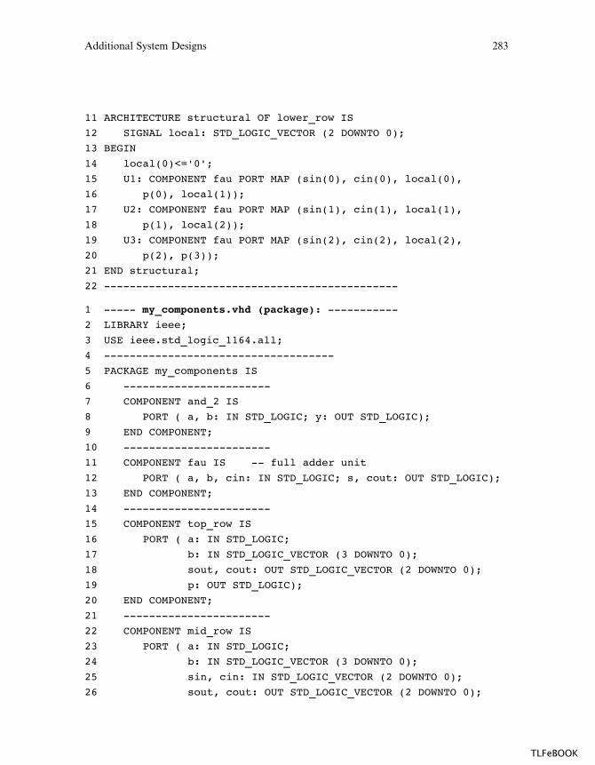
11 ARCHITECTURE structural OF lower_row IS
12 SIGNAL local: STD_LOGIC_VECTOR (2 DOWNTO 0);
13 BEGIN
14 local(0)<='0';
15 U1: COMPONENT fau PORT MAP (sin(0), cin(0), local(0),
16 p(0), local(1));
17 U2: COMPONENT fau PORT MAP (sin(1), cin(1), local(1),
18 p(1), local(2));
19 U3: COMPONENT fau PORT MAP (sin(2), cin(2), local(2),
20 p(2), p(3));
21 END structural;
22 ----------------------------------------------
1 ----- my_components.vhd (package): -----------
2 LIBRARY ieee;
3 USE ieee.std_logic_1164.all;
4 ------------------------------------
5 PACKAGE my_components IS
6 -----------------------
7 COMPONENT and_2 IS
8 PORT ( a, b: IN STD_LOGIC; y: OUT STD_LOGIC);
9 END COMPONENT;
10 -----------------------
11 COMPONENT fau IS -- full adder unit
12 PORT ( a, b, cin: IN STD_LOGIC; s, cout: OUT STD_LOGIC);
13 END COMPONENT;
14 -----------------------
15 COMPONENT top_row IS
16 PORT ( a: IN STD_LOGIC;
17 b: IN STD_LOGIC_VECTOR (3 DOWNTO 0);
18 sout, cout: OUT STD_LOGIC_VECTOR (2 DOWNTO 0);
19 p: OUT STD_LOGIC);
20 END COMPONENT;
21 -----------------------
22 COMPONENT mid_row IS
23 PORT ( a: IN STD_LOGIC;
24 b: IN STD_LOGIC_VECTOR (3 DOWNTO 0);
25 sin, cin: IN STD_LOGIC_VECTOR (2 DOWNTO 0);
26 sout, cout: OUT STD_LOGIC_VECTOR (2 DOWNTO 0);
Additional System Designs 283
TLFeBOOK
27 p: OUT STD_LOGIC);
28 END COMPONENT;
29 -----------------------
30 COMPONENT lower_row IS
31 PORT ( sin, cin: IN STD_LOGIC_VECTOR (2 DOWNTO 0);
32 p: OUT STD_LOGIC_VECTOR (3 DOWNTO 0);
33 END COMPONENT;
34 -----------------------
35 END my_components;
36 ----------------------------------------------
1 ------- multiplier.vhd (project): ------------
2 LIBRARY ieee;
3 USE ieee.std_logic_1164.all;
4 USE work.my_components.all;
5 ---------------------------------------
6 ENTITY multiplier IS
7 PORT ( a, b: IN STD_LOGIC_VECTOR (3 DOWNTO 0);
8 prod: OUT STD_LOGIC_VECTOR (7 DOWNTO 0));
9 END multiplier;
10 ---------------------------------------
11 ARCHITECTURE structural OF multiplier IS
12 TYPE matrix IS ARRAY (0 TO 3) OF
13 STD_LOGIC_VECTOR (2 DOWNTO 0);
14 SIGNAL s, c: matrix;
15 BEGIN
16 U1: COMPONENT top_row PORT MAP (a(0), b, s(0), c(0),
17 prod(0));
18 U2: COMPONENT mid_row PORT MAP (a(1), b, s(0), c(0), s(1),
19 c(1), prod(1));
20 U3: COMPONENT mid_row PORT MAP (a(2), b, s(1), c(1), s(2),
21 c(2), prod(2));
22 U4: COMPONENT mid_row PORT MAP (a(3), b, s(2), c(2), s(3),
23 c(3), prod(3));
24 U5: COMPONENT lower_row PORT MAP (s(3), c(3),
25 prod(7 DOWNTO 4));
26 END structural;
27 ----------------------------------------------
284 Chapter 12
TLFeBOOK
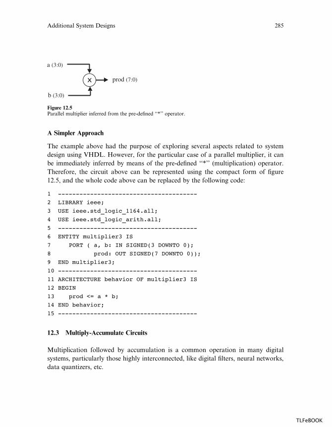
A Simpler Approach
The example above had the purpose of exploring several aspects related to system
design using VHDL. However, for the particular case of a parallel multiplier, it can
be immediately inferred by means of the pre-defined ‘‘*’’ (multiplication) operator.
Therefore, the circuit above can be represented using the compact form of figure
12.5, and the whole code above can be replaced by the following code:
1 ---------------------------------------
2 LIBRARY ieee;
3 USE ieee.std_logic_1164.all;
4 USE ieee.std_logic_arith.all;
5 ---------------------------------------
6 ENTITY multiplier3 IS
7 PORT ( a, b: IN SIGNED(3 DOWNTO 0);
8 prod: OUT SIGNED(7 DOWNTO 0));
9 END multiplier3;
10 ---------------------------------------
11 ARCHITECTURE behavior OF multiplier3 IS
12 BEGIN
13 prod <= a * b;
14 END behavior;
15 ---------------------------------------
12.3 Multiply-Accumulate Circuits
Multiplication followed by accumulation is a common operation in many digital
systems, particularly those highly interconnected, like digital filters, neural networks,
data quantizers, etc.
Figure 12.5Parallel multiplier inferred from the pre-defined ‘‘*’’ operator.
Additional System Designs 285
TLFeBOOK
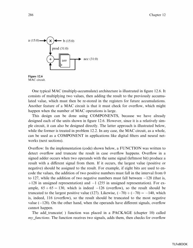
One typical MAC (multiply-accumulate) architecture is illustrated in figure 12.6. It
consists of multiplying two values, then adding the result to the previously accumu-
lated value, which must then be re-stored in the registers for future accumulations.
Another feature of a MAC circuit is that it must check for overflow, which might
happen when the number of MAC operations is large.
This design can be done using COMPONENTS, because we have already
designed each of the units shown in figure 12.6. However, since it is a relatively sim-
ple circuit, it can also be designed directly. The latter approach is illustrated below,
while the former is treated in problem 12.2. In any case, the MAC circuit, as a whole,
can be used as a COMPONENT in applications like digital filters and neural net-
works (next sections).
Overflow: In the implementation (code) shown below, a FUNCTION was written to
detect overflow and truncate the result in case overflow happens. Overflow in a
signed adder occurs when two operands with the same signal (leftmost bit) produce a
result with a di¤erent signal from them. If it occurs, the largest value (positive or
negative) should be assigned to the result. For example, if eight bits are used to en-
code the values, the addition of two positive numbers must fall in the interval from 0
to 127, while the addition of two negative numbers must fall between �128 (that is,
þ128 in unsigned representation) and �1 (255 in unsigned representation). For ex-
ample, 65þ 65 ¼ 130, which is indeed �126 (overflow), so the result should be
truncated to the largest positive value (127). Likewise, (�70)þ (�70) ¼ �140, which
is, indeed, 116 (overflow), so the result should be truncated to the most negative
value (�128). On the other hand, when the operands have di¤erent signals, overflow
cannot happen.
The add_truncate( ) function was placed in a PACKAGE (chapter 10) called
my_functions. The function receives two signals, adds them, then checks for overflow
Figure 12.6MAC circuit.
286 Chapter 12
TLFeBOOK
and truncates the result if necessary, returning the processed result to the main code.
Notice that the function is generic, for the number of bits of the operands is passed to
it by means of a parameter called size. Notice also in the main code that the param-
eters passed to the function were declared as signals (line 14), because variables are
not allowed (chapter 11).
1 ------- PACKAGE my_functions: -----------------------------
2 LIBRARY ieee;
3 USE ieee.std_logic_1164.all;
4 USE ieee.std_logic_arith.all;
5 ----------------------------------------------------------
6 PACKAGE my_functions IS
7 FUNCTION add_truncate (SIGNAL a, b: SIGNED; size: INTEGER)
8 RETURN SIGNED;
9 END my_functions;
10 ----------------------------------------------------------
11 PACKAGE BODY my_functions IS
12 FUNCTION add_truncate (SIGNAL a, b: SIGNED; size: INTEGER)
13 RETURN SIGNED IS
14 VARIABLE result: SIGNED (7 DOWNTO 0);
15 BEGIN
16 result := a + b;
17 IF (a(a'left)=b(b'left)) AND
18 (result(result'LEFT)/=a(a'left)) THEN
19 result := (result'LEFT => a(a'LEFT),
20 OTHERS => NOT a(a'left));
21 END IF;
22 RETURN result;
23 END add_truncate;
24 END my_functions;
25 ----------------------------------------------------------
1 ------- Main code: -----------------------
2 LIBRARY ieee;
3 USE ieee.std_logic_1164.all;
4 USE ieee.std_logic_arith.all;
5 USE work.my_functions.all;
6 ------------------------------------------
Additional System Designs 287
TLFeBOOK
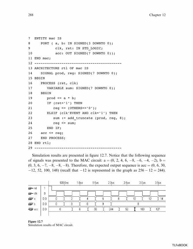
7 ENTITY mac IS
8 PORT ( a, b: IN SIGNED(3 DOWNTO 0);
9 clk, rst: IN STD_LOGIC;
10 acc: OUT SIGNED(7 DOWNTO 0));
11 END mac;
12 ------------------------------------------
13 ARCHITECTURE rtl OF mac IS
14 SIGNAL prod, reg: SIGNED(7 DOWNTO 0);
15 BEGIN
16 PROCESS (rst, clk)
17 VARIABLE sum: SIGNED(7 DOWNTO 0);
18 BEGIN
19 prod <= a * b;
20 IF (rst='1') THEN
21 reg <= (OTHERS=>'0');
22 ELSIF (clk'EVENT AND clk='1') THEN
23 sum := add_truncate (prod, reg, 8);
24 reg <= sum;
25 END IF;
26 acc <= reg;
27 END PROCESS;
28 END rtl;
29 ------------------------------------------
Simulation results are presented in figure 12.7. Notice that the following sequence
of signals was presented to the MAC circuit: a ¼ (0, 2, 4, 6, �8, �6, �4, �2), b ¼(0, 3, 6, �7, �8, �8, �8). Therefore, the expected output sequence is acc ¼ (0, 6, 30,
�12, 52, 100, 148) (recall that �12 is represented in the graph as 256� 12 ¼ 244).
Figure 12.7Simulation results of MAC circuit.
288 Chapter 12
TLFeBOOK
All the values are OK, except the last one, for it is above the maximum positive value
allowed for 8-bit signed numbers (127). Therefore, this result was kept at 127.
12.4 Digital Filters
Digital signal processing (DSP) finds innumerable applications in the fields of audio,
video, and communications, among others. Such applications are generally based on
LTI (linear time invariant) systems, which can be implemented with digital circuitry.
Any LTI system be represented by the following equation:
XN
k¼0
aky[n� k] ¼XM
k¼0
bkx[n� k]
where ak and bk are the filter coe‰cients, and x[n� k], y[n� k] are the current (for
k ¼ 0) and earlier (for k > 0) input and output values, respectively. To implement
this expression, registers are necessary to store x[n� k] and/or y[n� k] (for k > 0),
besides multipliers and adders, which are well-known building blocks in the digital
domain.
The impulse response of a digital filter can be divided into two categories: IIR
(infinite impulse response) and FIR (finite impulse response). The former corre-
sponds to the general case described by the equation above, while the latter occurs
when N ¼ 0. Only FIR filters can exhibit linear phase, so they are indispensable
when linear phase is required, like in many telecom applications. With N ¼ 0, the
equation above becomes
y[n] ¼XM
k¼0
ckx[n� k]
where ck ¼ bk/a0 are the coe‰cients of the FIR filter. This equation can be imple-
mented by the system of figure 12.8, where D (delay) represents a register (flip-flops),
a triangle is a multiplier, and a circle means an adder.
An equivalent RTL representation is shown in figure 12.9. As shown, the values of
x are stored in a shift register, whose outputs are connected to multipliers and then to
adders. The coe‰cients must also be stored on chip. However, if the coe‰cients are
always the same (that is, if it is a dedicated filter), their values can be implemented by
means of logic gates rather than registers (we just need to store CONSTANTS). On
the other hand, if it is a general purpose filter, then registers are required for the
coe‰cients. In the architecture of figure 12.9, the output vector (y) was also stored, in
order to provide a clean, synchronous output.
Additional System Designs 289
TLFeBOOK

The circuit of figure 12.9 can be constructed in several ways. However, if it is
intended for future reuse or sharing, than it should be as generic as possible. In the
code presented below, two GENERIC parameters are specified (line 7): n defines the
number of filter coe‰cients, while m specifies the number of bits used to represent
the input and coe‰cients. For the output, 2 m bits were used. Thus, for example,
16 bits could be used for x, coef, and reg, while 32 bits could be used for all other
signals (from the outputs of the multipliers all the way to y).
Notice that the lower section of the filter contains a MAC (multiply-accumulate)
pipeline. This circuit is closely related to the MAC circuit discussed in section 12.3.
Here too, overflow can happen, so an add/truncate procedure must be included in
the design.
x[n]co
D
c1
+
+
c2
+
c3
D
D
y[n]
x[n-1]
x[n-2]
x[n-3]
Figure 12.8FIR filter diagram (with 4 coe‰cients).
Figure 12.9RTL representation of a FIR filter.
290 Chapter 12
TLFeBOOK
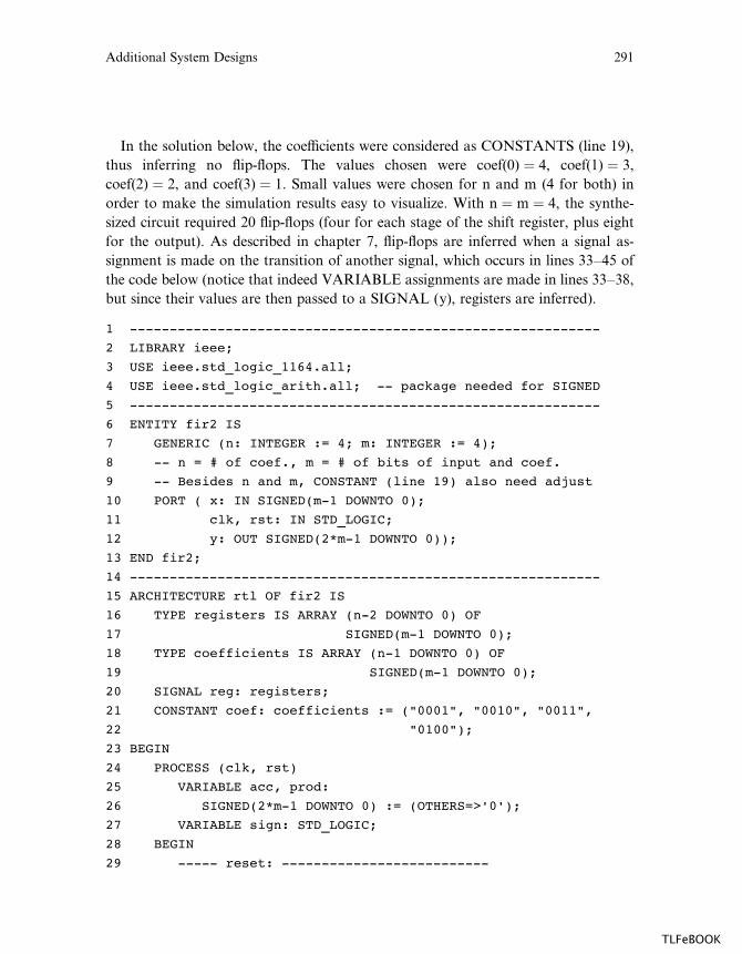
In the solution below, the coe‰cients were considered as CONSTANTS (line 19),
thus inferring no flip-flops. The values chosen were coef(0) ¼ 4, coef(1) ¼ 3,
coef(2) ¼ 2, and coef(3) ¼ 1. Small values were chosen for n and m (4 for both) in
order to make the simulation results easy to visualize. With n ¼ m ¼ 4, the synthe-
sized circuit required 20 flip-flops (four for each stage of the shift register, plus eight
for the output). As described in chapter 7, flip-flops are inferred when a signal as-
signment is made on the transition of another signal, which occurs in lines 33–45 of
the code below (notice that indeed VARIABLE assignments are made in lines 33–38,
but since their values are then passed to a SIGNAL (y), registers are inferred).
1 -----------------------------------------------------------
2 LIBRARY ieee;
3 USE ieee.std_logic_1164.all;
4 USE ieee.std_logic_arith.all; -- package needed for SIGNED
5 -----------------------------------------------------------
6 ENTITY fir2 IS
7 GENERIC (n: INTEGER := 4; m: INTEGER := 4);
8 -- n = # of coef., m = # of bits of input and coef.
9 -- Besides n and m, CONSTANT (line 19) also need adjust
10 PORT ( x: IN SIGNED(m-1 DOWNTO 0);
11 clk, rst: IN STD_LOGIC;
12 y: OUT SIGNED(2*m-1 DOWNTO 0));
13 END fir2;
14 -----------------------------------------------------------
15 ARCHITECTURE rtl OF fir2 IS
16 TYPE registers IS ARRAY (n-2 DOWNTO 0) OF
17 SIGNED(m-1 DOWNTO 0);
18 TYPE coefficients IS ARRAY (n-1 DOWNTO 0) OF
19 SIGNED(m-1 DOWNTO 0);
20 SIGNAL reg: registers;
21 CONSTANT coef: coefficients := ("0001", "0010", "0011",
22 "0100");
23 BEGIN
24 PROCESS (clk, rst)
25 VARIABLE acc, prod:
26 SIGNED(2*m-1 DOWNTO 0) := (OTHERS=>'0');
27 VARIABLE sign: STD_LOGIC;
28 BEGIN
29 ----- reset: --------------------------
Additional System Designs 291
TLFeBOOK
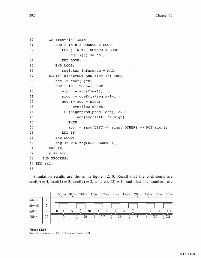
30 IF (rst='1') THEN
31 FOR i IN n-2 DOWNTO 0 LOOP
32 FOR j IN m-1 DOWNTO 0 LOOP
33 reg(i)(j) <= '0';
34 END LOOP;
35 END LOOP;
36 ----- register inference + MAC: -------
37 ELSIF (clk'EVENT AND clk='1') THEN
38 acc := coef(0)*x;
39 FOR i IN 1 TO n-1 LOOP
40 sign := acc(2*m-1);
41 prod := coef(i)*reg(n-1-i);
42 acc := acc + prod;
43 ---- overflow check: ------------
44 IF (sign=prod(prod'left)) AND
45 (acc(acc'left) /= sign)
46 THEN
47 acc := (acc'LEFT => sign, OTHERS => NOT sign);
48 END IF;
49 END LOOP;
50 reg <= x & reg(n-2 DOWNTO 1);
51 END IF;
52 y <= acc;
53 END PROCESS;
54 END rtl;
55 -----------------------------------------------------------
Simulation results are shown in figure 12.10. Recall that the coe‰cients are
coef(0) ¼ 4, coef(1) ¼ 3, coef(2) ¼ 2, and coef(3) ¼ 1, and that the numbers are
Figure 12.10Simulation results of FIR filter of figure 12.9.
292 Chapter 12
TLFeBOOK
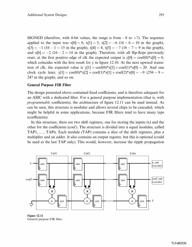
SIGNED (therefore, with 4-bit values, the range is from �8 to þ7). The sequence
applied to the input was x[0] ¼ 0, x[1] ¼ 5, x[2] ¼ �6 (16� 6 ¼ 10 in the graph),
x[3] ¼ �1 (16� 1 ¼ 15 in the graph), x[4] ¼ 4, x[5] ¼ �7 (16� 7 ¼ 9 in the graph),
and x[6] ¼ �2 (16� 2 ¼ 14 in the graph). Therefore, with all flip-flops previously
reset, at the first positive edge of clk the expected output is y[0] ¼ coef(0)*x[0] ¼ 0,
which coincides with the first result for y in figure 12.10. At the next upward transi-
tion of clk, the expected value is y[1] ¼ coef(0)*x[1]þ coef(1)*x[0] ¼ 20. And one
clock cycle later, y[1] ¼ coef(0)*x[2]þ coef(1)*x[1] þ coef(2)*x[0] ¼ �9 (256� 9 ¼247 in the graph), and so on.
General Purpose FIR Filter
The design presented above contained fixed coe‰cients, and is therefore adequate for
an ASIC with a dedicated filter. For a general purpose implementation (that is, with
programmable coe‰cients), the architecture of figure 12.11 can be used instead. As
can be seen, this structure is modular and allows several chips to be cascaded, which
might be helpful in some applications, because FIR filters tend to have many taps
(coe‰cients).
In this structure, there are two shift registers, one for storing the inputs (x) and the
other for the coe‰cients (coef ). The structure is divided into n equal modules, called
TAP1, . . . , TAPn. Each module (TAP) contains a slice of the shift registers, plus a
multiplier and an adder. It also contains an output register, but this is optional (could
be used at the last TAP only). This would, however, increase the ripple propagation
Figure 12.11General purpose FIR filter.
Additional System Designs 293
TLFeBOOK
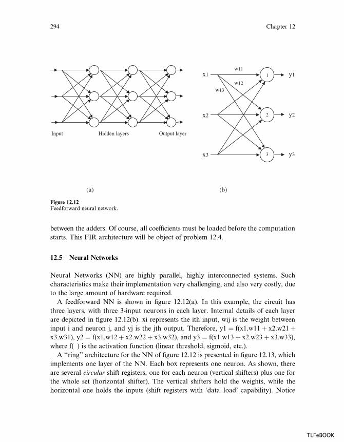
between the adders. Of course, all coe‰cients must be loaded before the computation
starts. This FIR architecture will be object of problem 12.4.
12.5 Neural Networks
Neural Networks (NN) are highly parallel, highly interconnected systems. Such
characteristics make their implementation very challenging, and also very costly, due
to the large amount of hardware required.
A feedforward NN is shown in figure 12.12(a). In this example, the circuit has
three layers, with three 3-input neurons in each layer. Internal details of each layer
are depicted in figure 12.12(b). xi represents the ith input, wij is the weight between
input i and neuron j, and yj is the jth output. Therefore, y1 ¼ f(x1.w11þ x2.w21þx3.w31), y2 ¼ f(x1.w12þ x2.w22þ x3.w32), and y3 ¼ f(x1.w13þ x2.w23þ x3.w33),
where f( ) is the activation function (linear threshold, sigmoid, etc.).
A ‘‘ring’’ architecture for the NN of figure 12.12 is presented in figure 12.13, which
implements one layer of the NN. Each box represents one neuron. As shown, there
are several circular shift registers, one for each neuron (vertical shifters) plus one for
the whole set (horizontal shifter). The vertical shifters hold the weights, while the
horizontal one holds the inputs (shift registers with ‘data_load’ capability). Notice
(a) (b)
Input Hidden layers Output layer
x1
x2
x3
y1
y2
y3
w11
w12
w13
1
2
3
Figure 12.12Feedforward neural network.
294 Chapter 12
TLFeBOOK
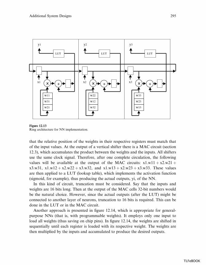
that the relative position of the weights in their respective registers must match that
of the input values. At the output of a vertical shifter there is a MAC circuit (section
12.3), which accumulates the product between the weights and the inputs. All shifters
use the same clock signal. Therefore, after one complete circulation, the following
values will be available at the output of the MAC circuits: x1.w11þ x2.w21þx3.w31, x1.w12þ x2.w22þ x3.w32, and x1.w13þ x2.w23þ x3.w33. These values
are then applied to a LUT (lookup table), which implements the activation function
(sigmoid, for example), thus producing the actual outputs, yi, of the NN.
In this kind of circuit, truncation must be considered. Say that the inputs and
weights are 16 bits long. Then at the output of the MAC cells 32-bit numbers would
be the natural choice. However, since the actual outputs (after the LUT) might be
connected to another layer of neurons, truncation to 16 bits is required. This can be
done in the LUT or in the MAC circuit.
Another approach is presented in figure 12.14, which is appropriate for general-
purpose NNs (that is, with programmable weights). It employs only one input to
load all weights (thus saving on chip pins). In figure 12.14, the weights are shifted in
sequentially until each register is loaded with its respective weight. The weights are
then multiplied by the inputs and accumulated to produce the desired outputs.
Figure 12.13Ring architecture for NN implementation.
Additional System Designs 295
TLFeBOOK
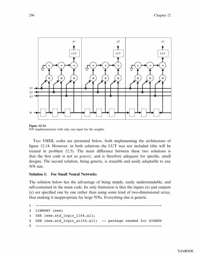
Two VHDL codes are presented below, both implementing the architecture of
figure 12.14. However, in both solutions the LUT was not included (this will be
treated in problem 12.5). The main di¤erence between these two solutions is
that the first code is not as generic, and is therefore adequate for specific, small
designs. The second solution, being generic, is reusable and easily adaptable to any
NN size.
Solution 1: For Small Neural Networks
The solution below has the advantage of being simple, easily understandable, and
self-contained in the main code. Its only limitation is that the inputs (x) and outputs
(y) are specified one by one rather than using some kind of two-dimensional array,
thus making it inappropriate for large NNs. Everything else is generic.
1 -----------------------------------------------------------
2 LIBRARY ieee;
3 USE ieee.std_logic_1164.all;
4 USE ieee.std_logic_arith.all; -- package needed for SIGNED
5 -----------------------------------------------------------
Figure 12.14NN implementation with only one input for the weights.
296 Chapter 12
TLFeBOOK
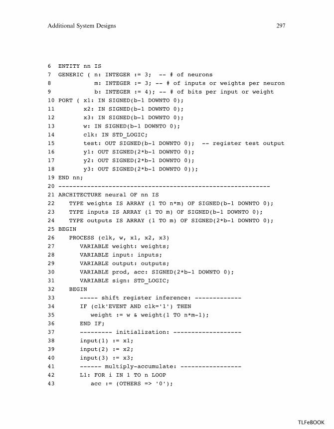
6 ENTITY nn IS
7 GENERIC ( n: INTEGER := 3; -- # of neurons
8 m: INTEGER := 3; -- # of inputs or weights per neuron
9 b: INTEGER := 4); -- # of bits per input or weight
10 PORT ( x1: IN SIGNED(b-1 DOWNTO 0);
11 x2: IN SIGNED(b-1 DOWNTO 0);
12 x3: IN SIGNED(b-1 DOWNTO 0);
13 w: IN SIGNED(b-1 DOWNTO 0);
14 clk: IN STD_LOGIC;
15 test: OUT SIGNED(b-1 DOWNTO 0); -- register test output
16 y1: OUT SIGNED(2*b-1 DOWNTO 0);
17 y2: OUT SIGNED(2*b-1 DOWNTO 0);
18 y3: OUT SIGNED(2*b-1 DOWNTO 0));
19 END nn;
20 -----------------------------------------------------------
21 ARCHITECTURE neural OF nn IS
22 TYPE weights IS ARRAY (1 TO n*m) OF SIGNED(b-1 DOWNTO 0);
23 TYPE inputs IS ARRAY (1 TO m) OF SIGNED(b-1 DOWNTO 0);
24 TYPE outputs IS ARRAY (1 TO m) OF SIGNED(2*b-1 DOWNTO 0);
25 BEGIN
26 PROCESS (clk, w, x1, x2, x3)
27 VARIABLE weight: weights;
28 VARIABLE input: inputs;
29 VARIABLE output: outputs;
30 VARIABLE prod, acc: SIGNED(2*b-1 DOWNTO 0);
31 VARIABLE sign: STD_LOGIC;
32 BEGIN
33 ----- shift register inference: -------------
34 IF (clk'EVENT AND clk='1') THEN
35 weight := w & weight(1 TO n*m-1);
36 END IF;
37 --------- initialization: -------------------
38 input(1) := x1;
39 input(2) := x2;
40 input(3) := x3;
41 ------ multiply-accumulate: -----------------
42 L1: FOR i IN 1 TO n LOOP
43 acc := (OTHERS => '0');
Additional System Designs 297
TLFeBOOK

44 L2: FOR j IN 1 TO m LOOP
45 prod := input(j)*weigth(m*(i-1)+j);
46 sign := acc(acc'LEFT);
47 acc := acc + prod;
48 ---- overflow check: -----------------
49 IF (sign=prod(prod'left)) AND
50 (acc(acc'left) /= sign) THEN
51 acc := (acc'LEFT => sign, OTHERS => NOT sign);
52 END IF;
53 END LOOP L2;
54 output(i) := acc;
55 END LOOP L1;
56 --------- outputs: --------------------------
57 test <= weight(n*m);
58 y1 <= output(1);
59 y2 <= output(2);
60 y3 <= output(3);
61 END PROCESS;
62 END neural;
63 -----------------------------------------------------------------
Simulation results are shown in figure 12.15. Notice that a small number of bits
and a small quantity of neurons were used in order to ease the visualization of the
simulation results. As can be seen in lines 7–9 of the code above, the NN has three
neurons with three 4-bit inputs each. Since type SIGNED was employed, the range
Figure 12.15Simulation results of NN implemented in solution 1.
298 Chapter 12
TLFeBOOK
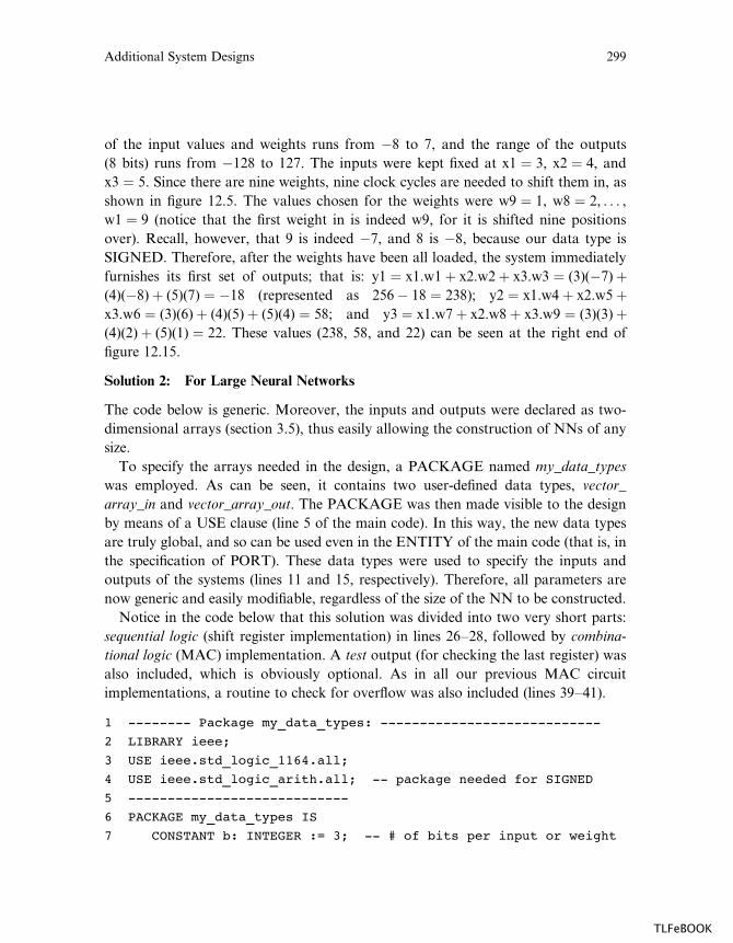
of the input values and weights runs from �8 to 7, and the range of the outputs
(8 bits) runs from �128 to 127. The inputs were kept fixed at x1 ¼ 3, x2 ¼ 4, and
x3 ¼ 5. Since there are nine weights, nine clock cycles are needed to shift them in, as
shown in figure 12.5. The values chosen for the weights were w9 ¼ 1, w8 ¼ 2, . . . ,
w1 ¼ 9 (notice that the first weight in is indeed w9, for it is shifted nine positions
over). Recall, however, that 9 is indeed �7, and 8 is �8, because our data type is
SIGNED. Therefore, after the weights have been all loaded, the system immediately
furnishes its first set of outputs; that is: y1 ¼ x1.w1þ x2.w2þ x3.w3 ¼ (3)(�7)þ(4)(�8)þ (5)(7) ¼ �18 (represented as 256� 18 ¼ 238); y2 ¼ x1.w4þ x2.w5þx3.w6 ¼ (3)(6)þ (4)(5)þ (5)(4) ¼ 58; and y3 ¼ x1.w7þ x2.w8þ x3.w9 ¼ (3)(3)þ(4)(2)þ (5)(1) ¼ 22. These values (238, 58, and 22) can be seen at the right end of
figure 12.15.
Solution 2: For Large Neural Networks
The code below is generic. Moreover, the inputs and outputs were declared as two-
dimensional arrays (section 3.5), thus easily allowing the construction of NNs of any
size.
To specify the arrays needed in the design, a PACKAGE named my_data_types
was employed. As can be seen, it contains two user-defined data types, vector_
array_in and vector_array_out. The PACKAGE was then made visible to the design
by means of a USE clause (line 5 of the main code). In this way, the new data types
are truly global, and so can be used even in the ENTITY of the main code (that is, in
the specification of PORT). These data types were used to specify the inputs and
outputs of the systems (lines 11 and 15, respectively). Therefore, all parameters are
now generic and easily modifiable, regardless of the size of the NN to be constructed.
Notice in the code below that this solution was divided into two very short parts:
sequential logic (shift register implementation) in lines 26–28, followed by combina-
tional logic (MAC) implementation. A test output (for checking the last register) was
also included, which is obviously optional. As in all our previous MAC circuit
implementations, a routine to check for overflow was also included (lines 39–41).
1 -------- Package my_data_types: ----------------------------
2 LIBRARY ieee;
3 USE ieee.std_logic_1164.all;
4 USE ieee.std_logic_arith.all; -- package needed for SIGNED
5 ----------------------------
6 PACKAGE my_data_types IS
7 CONSTANT b: INTEGER := 3; -- # of bits per input or weight
Additional System Designs 299
TLFeBOOK
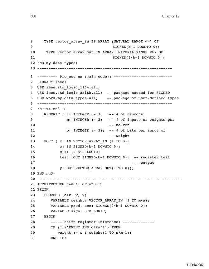
8 TYPE vector_array_in IS ARRAY (NATURAL RANGE <>) OF
9 SIGNED(b-1 DOWNTO 0);
10 TYPE vector_array_out IS ARRAY (NATURAL RANGE <>) OF
11 SIGNED(2*b-1 DOWNTO 0);
12 END my_data_types;
13 ------------------------------------------------------------
1 --------- Project nn (main code): --------------------------
2 LIBRARY ieee;
3 USE ieee.std_logic_1164.all;
4 USE ieee.std_logic_arith.all; -- package needed for SIGNED
5 USE work.my_data_types.all; -- package of user-defined types
6 ------------------------------------------------------------
7 ENTITY nn3 IS
8 GENERIC ( n: INTEGER := 3; -- # of neurons
9 m: INTEGER := 3; -- # of inputs or weights per
10 -- neuron
11 b: INTEGER := 3); -- # of bits per input or
12 -- weight
13 PORT ( x: IN VECTOR_ARRAY_IN (1 TO m);
14 w: IN SIGNED(b-1 DOWNTO 0);
15 clk: IN STD_LOGIC;
16 test: OUT SIGNED(b-1 DOWNTO 0); -- register test
17 -- output
18 y: OUT VECTOR_ARRAY_OUT(1 TO n));
19 END nn3;
20 ----------------------------------------------------------------
21 ARCHITECTURE neural OF nn3 IS
22 BEGIN
23 PROCESS (clk, w, x)
24 VARIABLE weight: VECTOR_ARRAY_IN (1 TO m*n);
25 VARIABLE prod, acc: SIGNED(2*b-1 DOWNTO 0);
26 VARIABLE sign: STD_LOGIC;
27 BEGIN
28 ----- shift register inference: --------------
29 IF (clk'EVENT AND clk='1') THEN
30 weight := w & weight(1 TO n*m-1);
31 END IF;
300 Chapter 12
TLFeBOOK

32 test <= weight(n*m);
33 ---- initialization: -------------------------
34 acc := (OTHERS => '0');
35 ------ multiply-accumulate: ------------------
36 L1: FOR i IN 1 TO n LOOP
37 L2: FOR j IN 1 TO m LOOP
38 prod := x(j)*weight(m*(i-1)+j);
39 sign := acc(acc'LEFT);
40 acc := acc + prod;
41 ---- overflow check: ------------------
42 IF (sign=prod(prod'LEFT)) AND
43 (acc(acc'LEFT)/=sign) THEN
44 acc := (acc’LEFT => sign, OTHERS => NOT sign);
45 END IF;
46 END LOOP L2;
47 ------ output: ---------------------------
48 y(i) <= acc;
49 acc := (OTHERS => ’0’);
50 END LOOP L1;
51 END PROCESS;
52 END neural;
53 -----------------------------------------------------------------
Other aspects related to the design of NNs will be treated in problem 12.5.
12.6 Problems
This section contains a series of problems regarding the use of system-level VHDL
units (PACKAGES, COMPONENTS, FUNCTIONS, and PROCEDURES).
Problem 12.1: Parallel Multiplier
We have seen, in section 12.2, the implementation of a parallel multiplier from
scratch. It was also mentioned that the pre-defined ‘‘*’’ (multiplication) operator
implements a parallel multiplier too. Though there are several architectures for such
a circuit (one was shown in figure 12.3), it is reasonable to assume that the amount of
hardware necessary to implement either solution presented in section 12.2 (from
scratch or using ‘‘*’’) should not di¤er substantially. You are asked to synthesize
Additional System Designs 301
TLFeBOOK
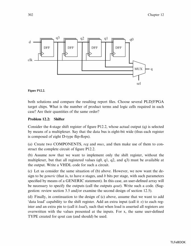
both solutions and compare the resulting report files. Choose several PLD/FPGA
target chips. What is the number of product terms and logic cells required in each
case? Are their quantities of the same order?
Problem 12.2: Shifter
Consider the 4-stage shift register of figure P12.2, whose actual output (q) is selected
by means of a multiplexer. Say that the data bus is eight-bit wide (thus each register
is composed of eight D-type flip-flops).
(a) Create two COMPONENTS, reg and mux, and then make use of them to con-
struct the complete circuit of figure P12.2.
(b) Assume now that we want to implement only the shift register, without the
multiplexer, but that all registered values (q0, q1, q2, and q3) must be available at
the output. Write a VHDL code for such a circuit.
(c) Let us consider the same situation of (b) above. However, we now want the de-
sign to be generic (that is, to have n stages, and b bits per stage, with such parameters
specified by means of a GENERIC statement). In this case, an user-defined array will
be necessary to specify the outputs (call the outputs qout). Write such a code. (Sug-
gestion: review section 3.5 and/or examine the second design of section 12.5).
(d) Finally, in continuation to the design of (c) above, assume that we want to add
‘data load’ capability to the shift register. Add an extra input (call it x) to each reg-
ister and an extra pin to (call it load ), such that when load is asserted all registers are
overwritten with the values presented at the inputs. For x, the same user-defined
TYPE created for qout can (and should) be used.
q0q1q2q3
DFF
d
clk
DFF
q
sel
DFFDFF
MUX
Figure P12.2.
302 Chapter 12
TLFeBOOK
Problem 12.3: MAC Circuit
In section 12.3, we studied the implementation of a MAC (multiply-accumulate) cir-
cuit (figure 12.6). In the implementation shown there, a FUNCTION was employed,
but COMPONENTS were not. Write another solution, this time using COMPO-
NENTS (multiplier, adder, and register). Create the components, then instantiate
them in the main code. Compile and simulate your project, comparing your results
with those obtained in figure 12.7
Problem 12.4: General Purpose FIR Filter
In section 12.4, we discussed the implementation of FIR filters. One complete design
was presented, in which the coe‰cients of the filter were fixed (figure 12.9). For a
general purpose filter (programmable coe‰cients), a modular architecture was sug-
gested in figure 12.11. You are asked to write a VHDL code for that filter. As a
suggestion, review first sections 12.3 and 12.4. Do not forget to include overflow
check in your design. Consider that the number of bits of all signals from the input
(x and coef ) up to the multiplier inputs is m, and 2m from there on (that is, from the
multiplier outputs up to y). Consider also that the number of taps (stages) is n. Write
a code as generic as possible. Then synthesize and simulate your circuit.
Problem 12.5: Neural Network
In section 12.5, we discussed the implementation of a highly interconnected system:
a neural network. Two architectures were presented, and two VHDL codes were
written regarding the second architecture. However, the LUT was not included in
those solutions. In this problem, the following is asked:
(a) Write a VHDL code that implements a LUT (you can choose the function to be
implemented, because what we want to practice here is how to implement a LUT).
Recall that a lookup table is simply a ROM (section 9.10).
(b) Write a VHDL code that implements the neural architecture depicted in figure
12.13. Then synthesize and simulate your solution to verify whether it works as
expected.
(c) There certainly are other ways of implementing a NN besides the two approaches
presented in section 12.5. Can you suggest another one? Can you suggest improve-
ments on the architectures and solutions presented there?
Additional System Designs 303
TLFeBOOK

TLFeBOOK

Appendix A: Programmable Logic Devices
A1. Introduction
Programmable Logic Devices (PLDs) were introduced in the mid 1970s. The idea
was to construct combinational logic circuits that were programmable. However,
contrary to microprocessors, which can run a program but posses a fixed hardware,
the programmability of PLDs was intended at the hardware level. In other words, a
PLD is a general purpose chip whose hardware can be reconfigured to meat particular
specifications.
The first PLDs were called PAL (Programmable Array Logic) or PLA (Program-
mable Logic Array), depending on the programming scheme (discussed later). They
used only logic gates (no flip-flops), thus allowing only the implementation of com-
binational circuits. To circumvent this problem, registered PLDs were launched soon
after, which included one flip-flop at each output of the circuit. With them, simple
sequential functions could then be implemented as well.
In the beginning of the 1980s, additional logic circuitry was added to each PLD
output. The new output cell, called Macrocell, contained (besides the flip-flop) logic
gates and multiplexers. Moreover, the cell itself was programmable, allowing several
modes of operation. Additionally, it provided a ‘return’ (feedback) signal from the
output of the circuit to the programmable array, which gave the PLD greater flexi-
bility. This new PLD structure was called generic PAL (GAL). A similar architecture
was known as PALCE (PAL CMOS Electrically erasable/programmable) device.
All these chips (PAL, PLA, registered PLD, and GAL/PALCE) are now collec-
tively referred to as SPLDs (Simple PLDs). The GAL/PALCE device is the only still
manufactured in a standalone package.
Later, several GAL devices were fabricated on the same chip, using a more so-
phisticated routing scheme, more advanced silicon technology, and several additional
features (like JTAG support and interface to several logic standards). This approach
became known as CPLD (Complex PLD). CPLDs are currently very popular due to
their high density, high performance, and low cost (CPLDs under a dollar can be
found).
Finally, in the mid 1980s, FPGAs (Field Programmable Gate Arrays) were intro-
duced. FPGAs di¤er from CPLDs in architecture, technology, built-in features, and
cost. They are aimed mainly at the implementation of large size, high-performance
circuits.
TLFeBOOK
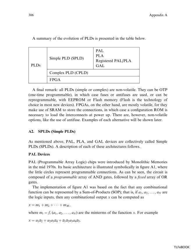
A summary of the evolution of PLDs is presented in the table below.
PLDs
Simple PLD (SPLD)
PAL
PLA
Registered PAL/PLA
GAL
Complex PLD (CPLD)
FPGA
A final remark: all PLDs (simple or complex) are non-volatile. They can be OTP
(one-time programmable), in which case fuses or antifuses are used, or can be
reprogrammable, with EEPROM or Flash memory (Flash is the technology of
choice in most new devices). FPGAs, on the other hand, are mostly volatile, for they
make use of SRAM to store the connections, in which case a configuration ROM is
necessary to load the interconnects at power up. There are, however, non-volatile
options, like the use of antifuse. Examples of each alternative will be shown later.
A2. SPLDs (Simple PLDs)
As mentioned above, PAL, PLA, and GAL devices are collectively called Simple
PLDs (SPLDs). A description of each of these architectures follows.
PAL Devices
PAL (Programmable Array Logic) chips were introduced by Monolithic Memories
in the mid 1970s. Its basic architecture is illustrated symbolically in figure A1, where
the little circles represent programmable connections. As can be seen, the circuit is
composed of a programmable array of AND gates, followed by a fixed array of OR
gates.
The implementation of figure A1 was based on the fact that any combinational
function can be represented by a Sum-of-Products (SOP); that is, if a1, a2, . . . , aN are
the logic inputs, then any combinational output x can be computed as
x ¼ m1 þm2 þ � � � þmM ;
where mi ¼ fi (a1, a2, . . . , aN ) are the minterms of the function x. For example
x ¼ a1a2 þ a2a3a4 þ a1a2a3a4a5:
306 Appendix A
TLFeBOOK

Hence, the products (minterms) can be obtained by means of AND gates, whose
outputs are then connected to an OR gate to compute their sum, thus implementing
the SOP equation described above.
The main limitation of this approach was the fact that it allowed only the imple-
mentation of combinational functions. To circumvent this problem, registered PALs
were launched toward the end of the 1970s. These included a flip-flop at each output
(after the OR gates in figure A1), thus allowing the implementation of sequential
functions as well (though only very simple ones).
An example of a then popular PAL chip is the PAL16L8 device, which contained
16 inputs and 8 outputs (though only 18 I/O pins were indeed available, because it
was a 20-pin DIP package; there were ten IN pins, two OUT pins, and six IN/OUT
outputs
inputs
programmableinterconnects
Figure A1Illustration of PAL architecture.
Programmable Logic Devices 307
TLFeBOOK
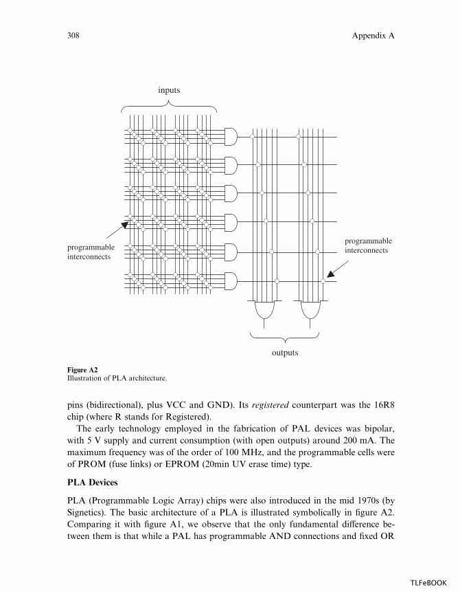
pins (bidirectional), plus VCC and GND). Its registered counterpart was the 16R8
chip (where R stands for Registered).
The early technology employed in the fabrication of PAL devices was bipolar,
with 5 V supply and current consumption (with open outputs) around 200 mA. The
maximum frequency was of the order of 100 MHz, and the programmable cells were
of PROM (fuse links) or EPROM (20min UV erase time) type.
PLA Devices
PLA (Programmable Logic Array) chips were also introduced in the mid 1970s (by
Signetics). The basic architecture of a PLA is illustrated symbolically in figure A2.
Comparing it with figure A1, we observe that the only fundamental di¤erence be-
tween them is that while a PAL has programmable AND connections and fixed OR
outputs
inputs
programmableinterconnects
programmableinterconnects
Figure A2Illustration of PLA architecture.
308 Appendix A
TLFeBOOK
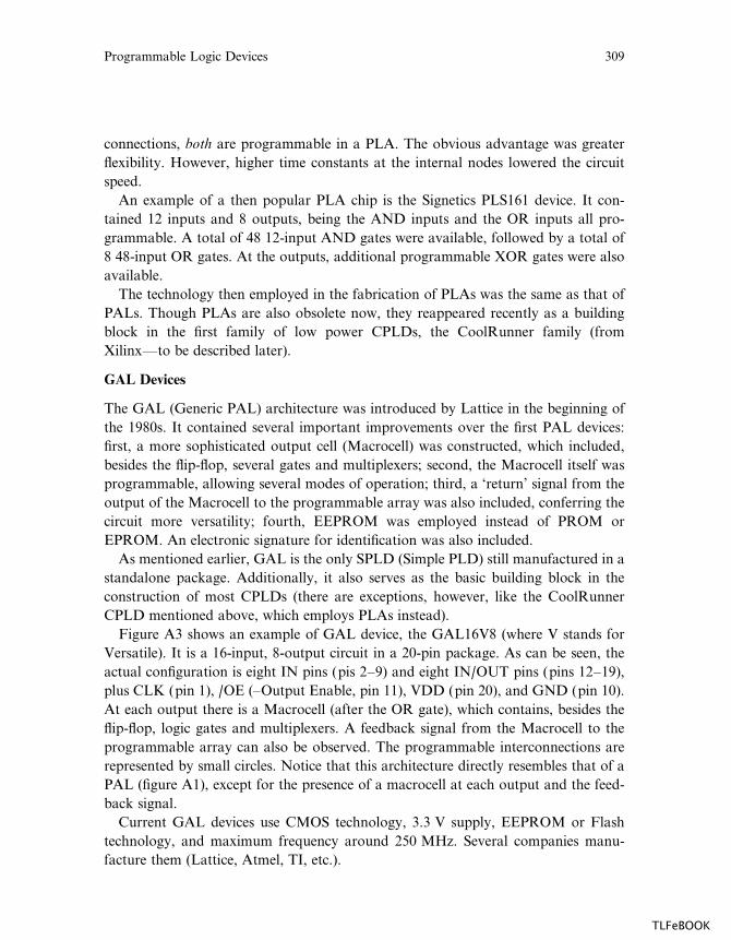
connections, both are programmable in a PLA. The obvious advantage was greater
flexibility. However, higher time constants at the internal nodes lowered the circuit
speed.
An example of a then popular PLA chip is the Signetics PLS161 device. It con-
tained 12 inputs and 8 outputs, being the AND inputs and the OR inputs all pro-
grammable. A total of 48 12-input AND gates were available, followed by a total of
8 48-input OR gates. At the outputs, additional programmable XOR gates were also
available.
The technology then employed in the fabrication of PLAs was the same as that of
PALs. Though PLAs are also obsolete now, they reappeared recently as a building
block in the first family of low power CPLDs, the CoolRunner family (from
Xilinx—to be described later).
GAL Devices
The GAL (Generic PAL) architecture was introduced by Lattice in the beginning of
the 1980s. It contained several important improvements over the first PAL devices:
first, a more sophisticated output cell (Macrocell) was constructed, which included,
besides the flip-flop, several gates and multiplexers; second, the Macrocell itself was
programmable, allowing several modes of operation; third, a ‘return’ signal from the
output of the Macrocell to the programmable array was also included, conferring the
circuit more versatility; fourth, EEPROM was employed instead of PROM or
EPROM. An electronic signature for identification was also included.
As mentioned earlier, GAL is the only SPLD (Simple PLD) still manufactured in a
standalone package. Additionally, it also serves as the basic building block in the
construction of most CPLDs (there are exceptions, however, like the CoolRunner
CPLD mentioned above, which employs PLAs instead).
Figure A3 shows an example of GAL device, the GAL16V8 (where V stands for
Versatile). It is a 16-input, 8-output circuit in a 20-pin package. As can be seen, the
actual configuration is eight IN pins (pis 2–9) and eight IN/OUT pins (pins 12–19),
plus CLK (pin 1), /OE (–Output Enable, pin 11), VDD (pin 20), and GND (pin 10).
At each output there is a Macrocell (after the OR gate), which contains, besides the
flip-flop, logic gates and multiplexers. A feedback signal from the Macrocell to the
programmable array can also be observed. The programmable interconnections are
represented by small circles. Notice that this architecture directly resembles that of a
PAL (figure A1), except for the presence of a macrocell at each output and the feed-
back signal.
Current GAL devices use CMOS technology, 3.3 V supply, EEPROM or Flash
technology, and maximum frequency around 250 MHz. Several companies manu-
facture them (Lattice, Atmel, TI, etc.).
Programmable Logic Devices 309
TLFeBOOK
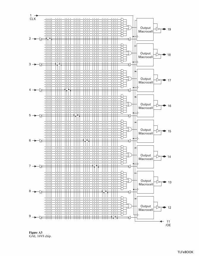
Figure A3GAL 16V8 chip.
TLFeBOOK
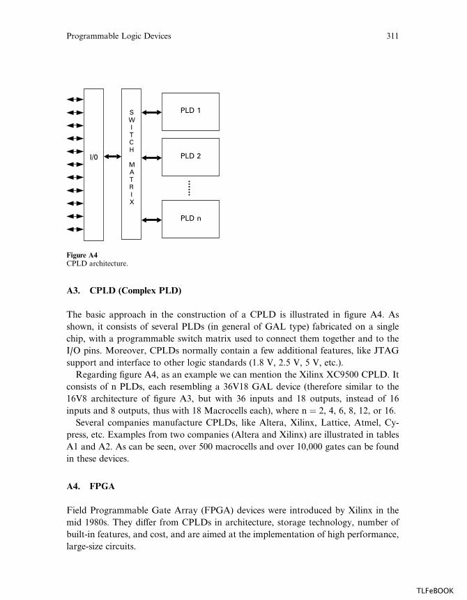
A3. CPLD (Complex PLD)
The basic approach in the construction of a CPLD is illustrated in figure A4. As
shown, it consists of several PLDs (in general of GAL type) fabricated on a single
chip, with a programmable switch matrix used to connect them together and to the
I/O pins. Moreover, CPLDs normally contain a few additional features, like JTAG
support and interface to other logic standards (1.8 V, 2.5 V, 5 V, etc.).
Regarding figure A4, as an example we can mention the Xilinx XC9500 CPLD. It
consists of n PLDs, each resembling a 36V18 GAL device (therefore similar to the
16V8 architecture of figure A3, but with 36 inputs and 18 outputs, instead of 16
inputs and 8 outputs, thus with 18 Macrocells each), where n ¼ 2, 4, 6, 8, 12, or 16.
Several companies manufacture CPLDs, like Altera, Xilinx, Lattice, Atmel, Cy-
press, etc. Examples from two companies (Altera and Xilinx) are illustrated in tables
A1 and A2. As can be seen, over 500 macrocells and over 10,000 gates can be found
in these devices.
A4. FPGA
Field Programmable Gate Array (FPGA) devices were introduced by Xilinx in the
mid 1980s. They di¤er from CPLDs in architecture, storage technology, number of
built-in features, and cost, and are aimed at the implementation of high performance,
large-size circuits.
Figure A4CPLD architecture.
Programmable Logic Devices 311
TLFeBOOK
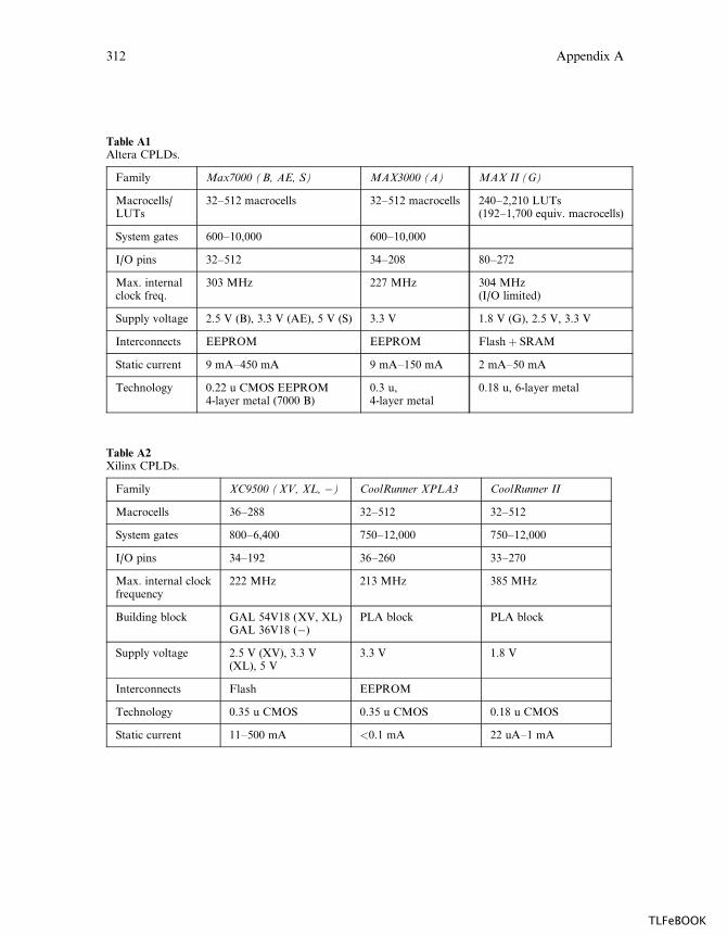
Table A1Altera CPLDs.
Family Max7000 (B, AE, S) MAX3000 (A) MAX II (G)
Macrocells/LUTs
32–512 macrocells 32–512 macrocells 240–2,210 LUTs(192–1,700 equiv. macrocells)
System gates 600–10,000 600–10,000
I/O pins 32–512 34–208 80–272
Max. internalclock freq.
303 MHz 227 MHz 304 MHz(I/O limited)
Supply voltage 2.5 V (B), 3.3 V (AE), 5 V (S) 3.3 V 1.8 V (G), 2.5 V, 3.3 V
Interconnects EEPROM EEPROM Flashþ SRAM
Static current 9 mA–450 mA 9 mA–150 mA 2 mA–50 mA
Technology 0.22 u CMOS EEPROM4-layer metal (7000 B)
0.3 u,4-layer metal
0.18 u, 6-layer metal
Table A2Xilinx CPLDs.
Family XC9500 (XV, XL, �) CoolRunner XPLA3 CoolRunner II
Macrocells 36–288 32–512 32–512
System gates 800–6,400 750–12,000 750–12,000
I/O pins 34–192 36–260 33–270
Max. internal clockfrequency
222 MHz 213 MHz 385 MHz
Building block GAL 54V18 (XV, XL)GAL 36V18 (�)
PLA block PLA block
Supply voltage 2.5 V (XV), 3.3 V(XL), 5 V
3.3 V 1.8 V
Interconnects Flash EEPROM
Technology 0.35 u CMOS 0.35 u CMOS 0.18 u CMOS
Static current 11–500 mA <0.1 mA 22 uA–1 mA
312 Appendix A
TLFeBOOK
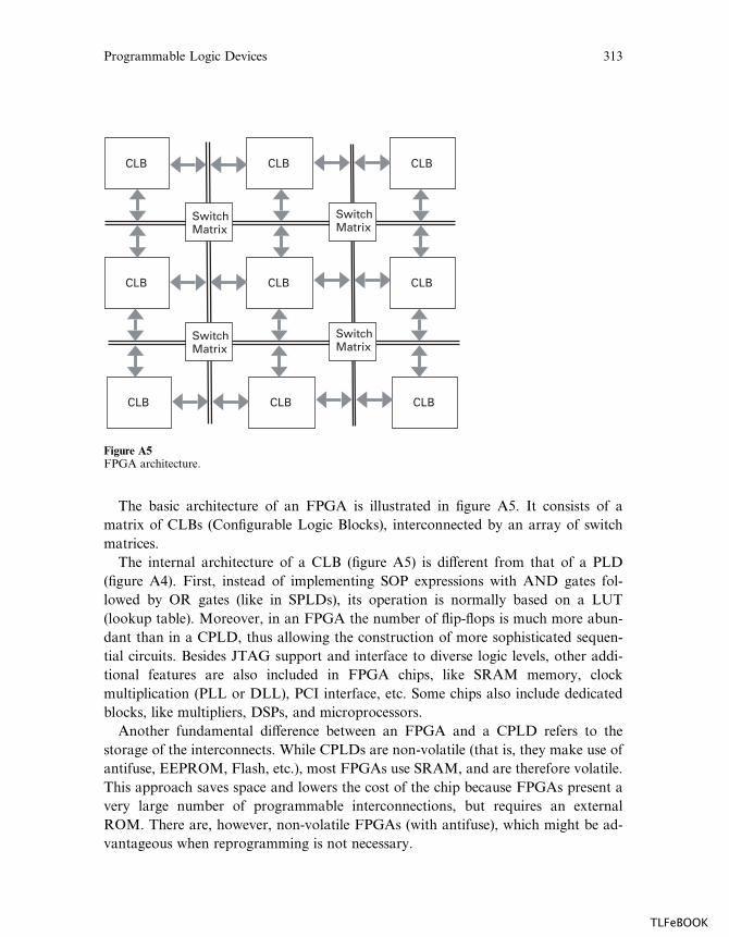
The basic architecture of an FPGA is illustrated in figure A5. It consists of a
matrix of CLBs (Configurable Logic Blocks), interconnected by an array of switch
matrices.
The internal architecture of a CLB (figure A5) is di¤erent from that of a PLD
(figure A4). First, instead of implementing SOP expressions with AND gates fol-
lowed by OR gates (like in SPLDs), its operation is normally based on a LUT
(lookup table). Moreover, in an FPGA the number of flip-flops is much more abun-
dant than in a CPLD, thus allowing the construction of more sophisticated sequen-
tial circuits. Besides JTAG support and interface to diverse logic levels, other addi-
tional features are also included in FPGA chips, like SRAM memory, clock
multiplication (PLL or DLL), PCI interface, etc. Some chips also include dedicated
blocks, like multipliers, DSPs, and microprocessors.
Another fundamental di¤erence between an FPGA and a CPLD refers to the
storage of the interconnects. While CPLDs are non-volatile (that is, they make use of
antifuse, EEPROM, Flash, etc.), most FPGAs use SRAM, and are therefore volatile.
This approach saves space and lowers the cost of the chip because FPGAs present a
very large number of programmable interconnections, but requires an external
ROM. There are, however, non-volatile FPGAs (with antifuse), which might be ad-
vantageous when reprogramming is not necessary.
Figure A5FPGA architecture.
Programmable Logic Devices 313
TLFeBOOK
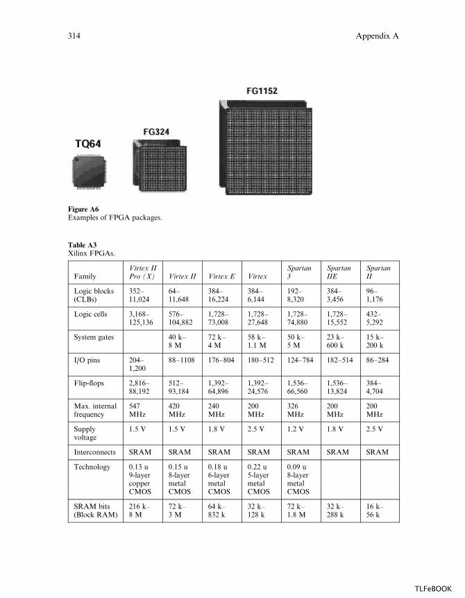
Figure A6Examples of FPGA packages.
Table A3Xilinx FPGAs.
FamilyVirtex IIPro (X) Virtex II Virtex E Virtex
Spartan3
SpartanIIE
SpartanII
Logic blocks(CLBs)
352–11,024
64–11,648
384–16,224
384–6,144
192–8,320
384–3,456
96–1,176
Logic cells 3,168–125,136
576–104,882
1,728–73,008
1,728–27,648
1,728–74,880
1,728–15,552
432–5,292
System gates 40 k–8 M
72 k–4 M
58 k–1.1 M
50 k–5 M
23 k–600 k
15 k–200 k
I/O pins 204–1,200
88–1108 176–804 180–512 124–784 182–514 86–284
Flip-flops 2,816–88,192
512–93,184
1,392–64,896
1,392–24,576
1,536–66,560
1,536–13,824
384–4,704
Max. internalfrequency
547MHz
420MHz
240MHz
200MHz
326MHz
200MHz
200MHz
Supplyvoltage
1.5 V 1.5 V 1.8 V 2.5 V 1.2 V 1.8 V 2.5 V
Interconnects SRAM SRAM SRAM SRAM SRAM SRAM SRAM
Technology 0.13 u9-layercopperCMOS
0.15 u8-layermetalCMOS
0.18 u6-layermetalCMOS
0.22 u5-layermetalCMOS
0.09 u8-layermetalCMOS
SRAM bits(Block RAM)
216 k–8 M
72 k–3 M
64 k–832 k
32 k–128 k
72 k–1.8 M
32 k–288 k
16 k–56 k
314 Appendix A
TLFeBOOK
FPGAs can be very sophisticated. Chips manufactured with state-of-the-art
0.09 mm CMOS technology, with nine copper layers and over 1,000 I/O pins, are
currently available. A few examples of FPGA packages are illustrated in figure A6,
which shows one of the smallest FPGA packages on the left (64 pins), a medium-size
package in the middle (324 pins), and a large package (1,152 pins) on the right.
Several companies manufacture FPGAs, like Xilinx, Actel, Altera, QuickLogic,
Atmel, etc. Examples from two companies (Xilinx and Actel) are illustrated in tables
A3 and A4. As can be seen, they can contain thousands of flip-flops and several
million gates.
Notice that all Xilinx FPGAs use SRAM to store the interconnects, so are re-
programmable, but volatile (thus requiring external ROM). On the other hand, Actel
FPGAs are non-volatile (they use antifuse), but are non-reprogrammable (except one
family, which uses Flash memory). Since each approach has its own advantages
and disadvantages, the actual application will dictate which chip architecture is most
appropriate.
Table A4Actel FPGAs.
Family Accelerator ProASIC MX SX eX
Logic modules 2,016–32,256 5,376–56,320 295–2,438 768–6,036 192–768
System gates 125 k–2 M 75 k–1 M 3 k–54 k 12 k–108 k 3 k–12 k
I/O pins 168–684 204–712 57–202 130–360 84–132
Flip-flops 1,344–21,504 5,376–26,880 147–1,822 512–4,024 128–512
Max. internalfrequency
500 MHz 250 MHz 250 MHz 350 MHz 350 MHz
Supply voltage 1.5 V 2.5 V, 3.3 V 3.3 V, 5 V 2.5 V, 3.3 V,5 V
2.5 V, 3.3 V,5 V
Interconnects Antifuse Flash Antifuse Antifuse Antifuse
Technology 0.15 u7-layer metalCMOS
0.22 u4-layer metalCMOS
0.45 um3-layer metalCMOS
0.22 uCMOS
0.22 uCMOS
SRAM bits 29 k–339 k 14 k–198 k 2.56 k n.a. n.a.
Programmable Logic Devices 315
TLFeBOOK

TLFeBOOK
Appendix B: Xilinx ISEBModelSim Tutorial
The following synthesis, placement, and simulation tools are described in the tuto-
rials presented in the Appendices:
Tools Application Appendix
ISE 6.1þModelSim 5.7c Xilinx CPLDs and FPGAs B
MaxPlus II 10.2þAdvanced
Synthesis Software
Altera CPLDs and some FPGAs C
Quartus II 3.0 Altera CPLDs and FPGAs D
XiIinx ISE 6.1 is a comprehensive synthesis and implementation environment for
Xilinx programmable devices. ModelSim XE 5.7c (from Model Technology) is also
provided as part of the package. The former is employed for circuit synthesis and
design implementation, while the latter is used for simulation.
Xilinx ISE 6.1 WebPack, along with ModelSim XE II 5.7c Starter, can be down-
loaded cost-free from www.xilinx.com.
This is a very brief tutorial, which is divided into five parts:
B1. Entering VHDL Code
B2. Synthesis and Implementation
B3. Creating Testbenches
B4. Simulation (with ModelSim)
B5. Physical Realization
B1. Entering VHDL Code
� Launch ISE 6.1 Project Navigator. A screen like that of figure B1 will be displayed.
� Start a new project (File ! New Project). The dialog box of figure B2 will be
shown. In the Project Name field, type the name of the ENTITY of the VHDL
code to be entered (flipflop, in this example). In the Project Location field, choose
the working directory. Finally, select HDL as the top level module type. Click on
Next.
� In the dialog box of figure B3, select the device (Spartan 3, for example). Then
select XST (Xilinx Synthesis Technology) as the synthesis tool, ModelSim as the
simulator, and VHDL as the language. Click on Next.
TLFeBOOK

Figure B1
Figure B2
318 Appendix B
TLFeBOOK

� In the dialog box of figure B4, select VHDL Module, then type the file name
(flipflop.vhd, in this example), and choose its location. Click on Next and Finish
until the text editor is displayed, as in figure B.5.
� Enter your VHDL code (figure B5) and save it. The project is now ready to be
synthesized.
B2. Synthesis and Implementation
� In the Processes for Source window, select Synthesize-XST. Then go to Process !Properties. The box of figure B6 will be shown. Select Optimization Goal ¼ Area
and Optimization E¤ort ¼ Normal, then click on OK.
� To synthesize the design, select Process ! Run, or click on , or double-click on
Synthesize-XST. However, if desired, the syntax can be checked before synthesis is
invoked. Just click on the ‘‘þ’’ sign before the word Synthesize-XST to expand it (see
figure B7) and double-click on Check Syntax.
� After synthesis is concluded, view the synthesis report. Double-click on View Syn-
thesis Report, under Synthesize-XST, in the Processes for Source window (figure B7).
To better view the report, you can use the toggle tool . A section of such a report is
presented in figure B8. Check, for example, the number of flip-flops inferred by the
compiler.
� Check also the RTL diagram. Double-click on View RTL Schematic, under the
Synthesize-XST directory. The diagram of figure B9 will be presented.
Figure B3
Xilinx ISEþModelSim Tutorial 319
TLFeBOOK
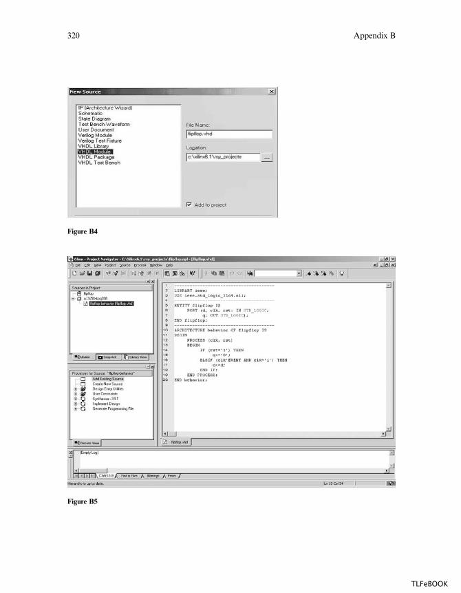
Figure B4
Figure B5
320 Appendix B
TLFeBOOK
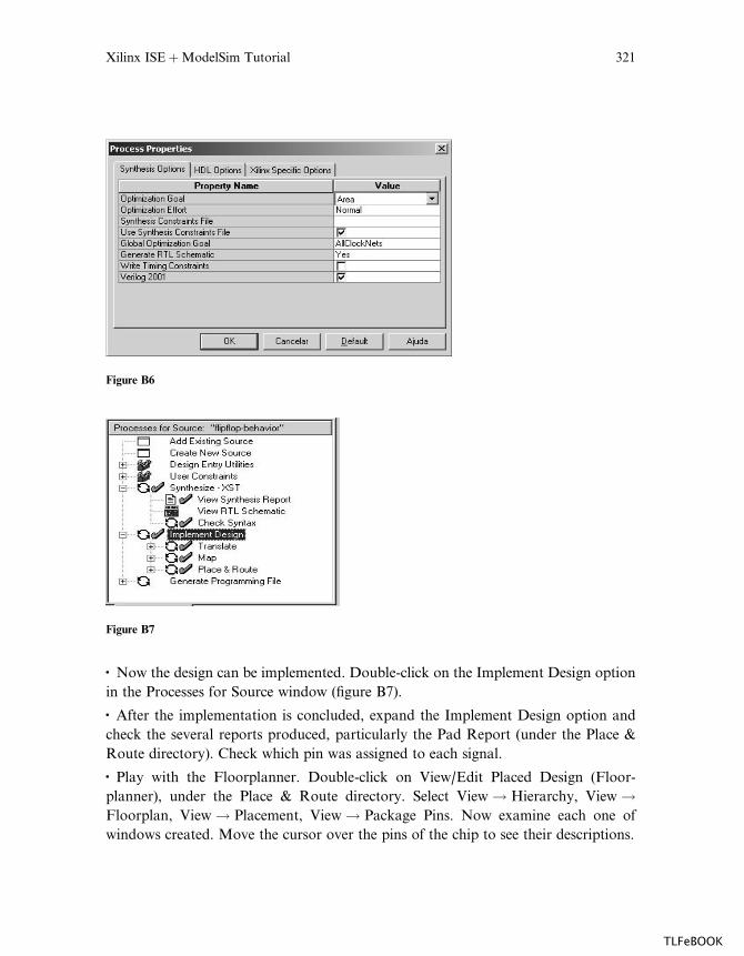
� Now the design can be implemented. Double-click on the Implement Design option
in the Processes for Source window (figure B7).
� After the implementation is concluded, expand the Implement Design option and
check the several reports produced, particularly the Pad Report (under the Place &
Route directory). Check which pin was assigned to each signal.
� Play with the Floorplanner. Double-click on View/Edit Placed Design (Floor-
planner), under the Place & Route directory. Select View ! Hierarchy, View !Floorplan, View ! Placement, View ! Package Pins. Now examine each one of
windows created. Move the cursor over the pins of the chip to see their descriptions.
Figure B6
Figure B7
Xilinx ISEþModelSim Tutorial 321
TLFeBOOK
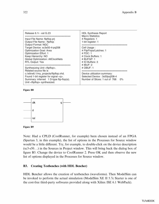
Note: Had a CPLD (CoolRunner, for example) been chosen instead of an FPGA
(Spartan 3, in this example), the list of options in the Processes for Source window
would be a little di¤erent. Try, for example, to double-click on the device description
(xc3-s50. . .) in the Sources in Project window. This will bring back the dialog box of
figure B3. Change the device to CoolRunner 2. Press OK and then observe the new
list of options displayed in the Processes for Source window.
B3. Creating Testbenches (with HDL Bencher)
HDL Bencher allows the creation of testbenches (waveforms). Then ModelSim can
be invoked to perform the actual simulation (ModelSim XE II 5.7c Starter is one of
the cost-free third-party softwares provided along with Xilinx ISE 6.1 WebPack).
Release 6.1i - xst G.23 =============================== Input File Name: flipflop.prjOutput File Name : flipflopOutput Format: NGC Target Device: xc3s50-4-pq208 Optimization Goal: Area Optimization Effort: 1 Keep Hierarchy: NO Global Optimization: AllClockNets RTL Output: Yes =============================== Synthesizing Unit <flipflop>. Related source file is c:/xilinx6.1/my_projects/flipflop.vhd.Found 1-bit register for signal <q>.Summary: inferred 1 D-type flip-flop(s). Unit <flipflop> synthesized.
HDL Synthesis ReportMacro Statistics# Registers: 1 1-bit register: 1 =============================== Cell Usage :# FlipFlops/Latches: 1# FDC: 1 # Clock Buffers: 1 # BUFGP: 1 # IO Buffers: 3# IBUF: 2# OBUF: 1 =============================== Device utilization summary: Selected Device : 3s50pq208-4 Number of Slices: 1 out of 768 0%
Figure B8
Figure B9
322 Appendix B
TLFeBOOK
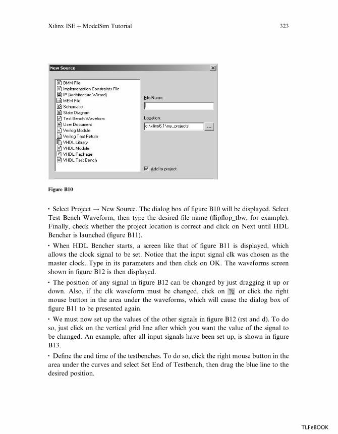
� Select Project ! New Source. The dialog box of figure B10 will be displayed. Select
Test Bench Waveform, then type the desired file name (flipflop_tbw, for example).
Finally, check whether the project location is correct and click on Next until HDL
Bencher is launched (figure B11).
� When HDL Bencher starts, a screen like that of figure B11 is displayed, which
allows the clock signal to be set. Notice that the input signal clk was chosen as the
master clock. Type in its parameters and then click on OK. The waveforms screen
shown in figure B12 is then displayed.
� The position of any signal in figure B12 can be changed by just dragging it up or
down. Also, if the clk waveform must be changed, click on or click the right
mouse button in the area under the waveforms, which will cause the dialog box of
figure B11 to be presented again.
� We must now set up the values of the other signals in figure B12 (rst and d). To do
so, just click on the vertical grid line after which you want the value of the signal to
be changed. An example, after all input signals have been set up, is shown in figure
B13.
� Define the end time of the testbenches. To do so, click the right mouse button in the
area under the curves and select Set End of Testbench, then drag the blue line to the
desired position.
Figure B10
Xilinx ISEþModelSim Tutorial 323
TLFeBOOK
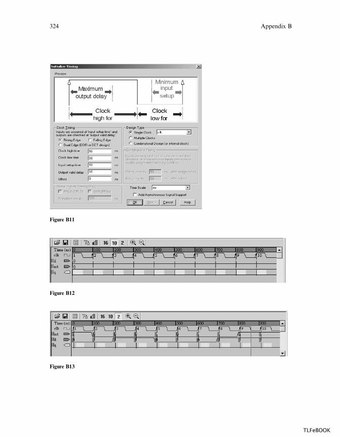
Figure B11
Figure B12
Figure B13
324 Appendix B
TLFeBOOK
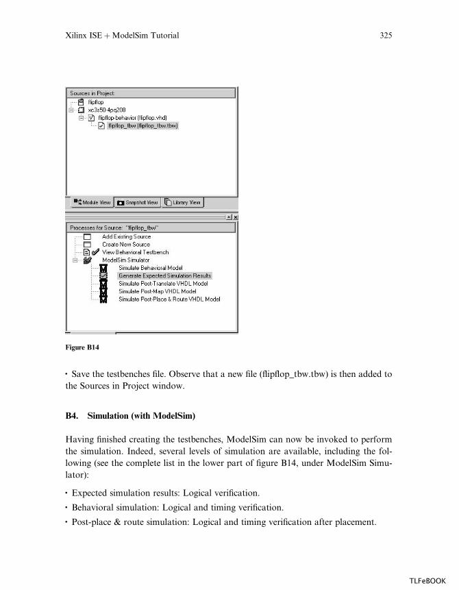
� Save the testbenches file. Observe that a new file (flipflop_tbw.tbw) is then added to
the Sources in Project window.
B4. Simulation (with ModelSim)
Having finished creating the testbenches, ModelSim can now be invoked to perform
the simulation. Indeed, several levels of simulation are available, including the fol-
lowing (see the complete list in the lower part of figure B14, under ModelSim Simu-
lator):
� Expected simulation results: Logical verification.
� Behavioral simulation: Logical and timing verification.
� Post-place & route simulation: Logical and timing verification after placement.
Figure B14
Xilinx ISEþModelSim Tutorial 325
TLFeBOOK
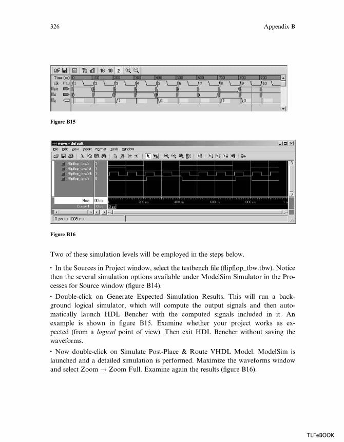
Two of these simulation levels will be employed in the steps below.
� In the Sources in Project window, select the testbench file (flipflop_tbw.tbw). Notice
then the several simulation options available under ModelSim Simulator in the Pro-
cesses for Source window (figure B14).
� Double-click on Generate Expected Simulation Results. This will run a back-
ground logical simulator, which will compute the output signals and then auto-
matically launch HDL Bencher with the computed signals included in it. An
example is shown in figure B15. Examine whether your project works as ex-
pected (from a logical point of view). Then exit HDL Bencher without saving the
waveforms.
� Now double-click on Simulate Post-Place & Route VHDL Model. ModelSim is
launched and a detailed simulation is performed. Maximize the waveforms window
and select Zoom ! Zoom Full. Examine again the results (figure B16).
Figure B15
Figure B16
326 Appendix B
TLFeBOOK
B5. Physical Realization
To physically implement the design in a CPLD or FPGA chip, a development kit is
necessary. Inexpensive alternatives are generally available through manufacturer’s
university programs, which o¤er design kits at low prices. Xilinx Digilab XC2, for
example, is a development kit for Xilinx CoolRunner II devices. The development kit
must be connected to a PC running ISE in order for the chip to be programmed.
Since the overall procedure of programming a chip is relatively similar from one
manufacturer to another, a detailed description will be presented in only two of the
appendices (C and D).
Xilinx ISEþModelSim Tutorial 327
TLFeBOOK

TLFeBOOK
Appendix C: Altera MaxPlus IIBAdvanced Synthesis Software Tutorial
The following synthesis, placement, and simulation tools are described in the tuto-
rials presented in the Appendices:
Tools Application Appendix
ISE 6.1þModelSim 5.7c Xilinx CPLDs and FPGAs B
MaxPlus II 10.2þAdvanced
Synthesis Software
Altera CPLDs and some FPGAs C
Quartus II 3.0 Altera CPLDs and FPGAs D
MaxPlus II 10.2 Baseline from Altera is a very simple, user-friendly synthesis and
simulation tool. Its main drawback is that it does not support several VHDL con-
structs, so only relatively simple code can be synthesized without the help of an ex-
ternal synthesis tool (like Leonardo Spectrum or Advanced Synthesis Software).
Additionally, it only covers Altera’s basic devices (its successor, Quartus II, described
in appendix D, covers all current devices). Still, due to its simplicity, it may be an
adequate starting point for first-time VHDL users. Moreover, with the recent release
of Advanced Synthesis Software, also a cost-free synthesis tool from Altera, using
MaxPlus II became more e¤ective because Advanced Synthesis Software does sup-
port most VHDL constructs. It can be used to synthesize the VHDL code, generating
an EDIF (.edf ) file which can then be imported by MaxPlus II for design imple-
mentation and simulation.
MaxPlus II 10.2 Baseline and Advanced Synthesis Software can be downloaded
cost-free from www.altera.com.
This is a very brief tutorial, which is divided into five parts:
C1. Entering VHDL Code
C2. Compilation
C3. Simulation
C4. Synthesis with Advanced Synthesis Software
C5. Physical Implementation
TLFeBOOK
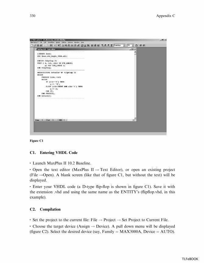
C1. Entering VHDL Code
� Launch MaxPlus II 10.2 Baseline.
� Open the text editor (MaxPlus II ! Text Editor), or open an existing project
(File !Open). A blank screen (like that of figure C1, but without the text) will be
displayed.
� Enter your VHDL code (a D-type flip-flop is shown in figure C1). Save it with
the extension .vhd and using the same name as the ENTITY’s (flipflop.vhd, in this
example).
C2. Compilation
� Set the project to the current file: File ! Project ! Set Project to Current File.
� Choose the target device (Assign ! Device). A pull down menu will be displayed
(figure C2). Select the desired device (say, Family ¼ MAX3000A, Device ¼ AUTO).
Figure C1
330 Appendix C
TLFeBOOK

� Set up the optimizer. The implementation can be optimized for speed or for area.
Select Assign ! Global Project Logic Synthesis and move the Optimize cursor all
the way to the left (value ¼ 0) to optimize for area, or all the way to the right
(value ¼ 10) to optimize for speed. Values in between can also be used.
� Click on the Compiler icon , then on Start, in order to execute the compilation.
� If no errors are detected, a screen like that of figure C3 is shown. It displays the files
created during the compilation in the upper part (notice, for example, the report
‘‘rpt’’ file icon), and information regarding the chip and fitter in the lower part.
� Open the report (.rpt) file (double-click on its icon, shown in figure C3). Verify at
least the following: pin assignments and number of logic cells and flip-flops used to
Figure C2
Figure C3
Altera MaxPlus IIþAdvanced Synthesis Software Tutorial 331
TLFeBOOK

R R E E S V S E C E R C R V r I G G G c G V E s N N N N l N E D t d T D D D k D q D -----------------------------------_
/ 6 5 4 3 2 1 44 43 42 41 40 | #TDI | 7 39 | RESERVED
RESERVED | 8 38 | #TDO RESERVED | 9 37 | RESERVED
GND | 10 36 | GND RESERVED | 11 35 | VCCIO RESERVED | 12 EPM3032ALC44-4 34 | RESERVED
#TMS | 13 33 | RESERVED RESERVED | 14 32 | #TCK VCCIO | 15 31 | RESERVED RESERVED | 16 30 | GND
GND | 17 29 | RESERVED |_ 18 19 20 21 22 23 24 25 26 27 28 _|
------------------------------------ R R R R G V R R R R R E E E E N C E E E E E S S S S D C S S S S S E E E E I E E E E E R R R R N R R R R R V V V V T V V V V V E E E E E E E E E D D D D D D D D D
Total bidirectional pins required: 0Total reserved pins required 4Total logic cells required: 1 Total flipflops required: 1Total product terms required: 2Total logic cells lending parallel expanders: 0Total shareable expanders in database: 0
Synthesized logic cells: 0/32 (0%)
Figure C4
332 Appendix C
TLFeBOOK
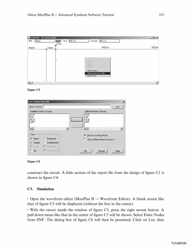
construct the circuit. A little section of the report file from the design of figure C1 is
shown in figure C4.
C3. Simulation
� Open the waveform editor (MaxPlus II ! Waveform Editor). A blank screen like
that of figure C5 will be displayed (without the box in the center).
� With the cursor inside the window of figure C5, press the right mouse button. A
pull down menu like that in the center of figure C5 will be shown. Select Enter Nodes
from SNF. The dialog box of figure C6 will then be presented. Click on List, then
Figure C5
Figure C6
Altera MaxPlus IIþAdvanced Synthesis Software Tutorial 333
TLFeBOOK
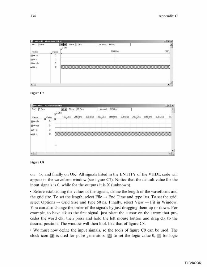
on ¼>, and finally on OK. All signals listed in the ENTITY of the VHDL code will
appear in the waveform window (see figure C7). Notice that the default value for the
input signals is 0, while for the outputs it is X (unknown).
� Before establishing the values of the signals, define the length of the waveforms and
the grid size. To set the length, select File ! End Time and type 1us. To set the grid,
select Options ! Grid Size and type 50 ns. Finally, select View ! Fit in Window.
You can also change the order of the signals by just dragging them up or down. For
example, to have clk as the first signal, just place the cursor on the arrow that pre-
cedes the word clk, then press and hold the left mouse button and drag clk to the
desired position. The window will then look like that of figure C8.
� We must now define the input signals, so the tools of figure C9 can be used. The
clock icon is used for pulse generators, to set the logic value 0, for logic
Figure C7
Figure C8
334 Appendix C
TLFeBOOK
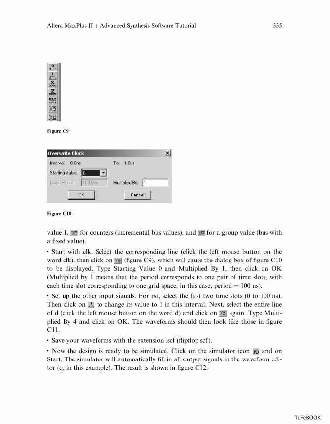
value 1, for counters (incremental bus values), and for a group value (bus with
a fixed value).
� Start with clk. Select the corresponding line (click the left mouse button on the
word clk), then click on (figure C9), which will cause the dialog box of figure C10
to be displayed. Type Starting Value 0 and Multiplied By 1, then click on OK
(Multiplied by 1 means that the period corresponds to one pair of time slots, with
each time slot corresponding to one grid space; in this case, period ¼ 100 ns).
� Set up the other input signals. For rst, select the first two time slots (0 to 100 ns).
Then click on to change its value to 1 in this interval. Next, select the entire line
of d (click the left mouse button on the word d) and click on again. Type Multi-
plied By 4 and click on OK. The waveforms should then look like those in figure
C11.
� Save your waveforms with the extension .scf (flipflop.scf ).
� Now the design is ready to be simulated. Click on the simulator icon and on
Start. The simulator will automatically fill in all output signals in the waveform edi-
tor (q, in this example). The result is shown in figure C12.
Figure C9
Figure C10
Altera MaxPlus IIþAdvanced Synthesis Software Tutorial 335
TLFeBOOK
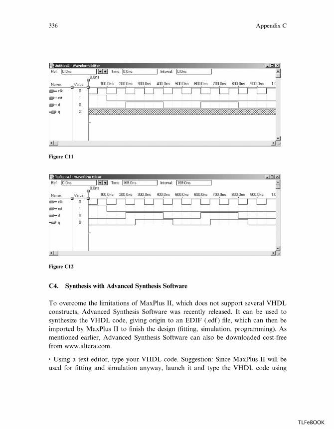
C4. Synthesis with Advanced Synthesis Software
To overcome the limitations of MaxPlus II, which does not support several VHDL
constructs, Advanced Synthesis Software was recently released. It can be used to
synthesize the VHDL code, giving origin to an EDIF (.edf ) file, which can then be
imported by MaxPlus II to finish the design (fitting, simulation, programming). As
mentioned earlier, Advanced Synthesis Software can also be downloaded cost-free
from www.altera.com.
� Using a text editor, type your VHDL code. Suggestion: Since MaxPlus II will be
used for fitting and simulation anyway, launch it and type the VHDL code using
Figure C11
Figure C12
336 Appendix C
TLFeBOOK
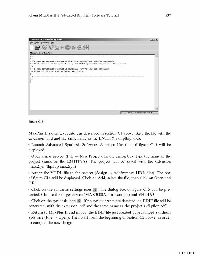
MaxPlus II’s own text editor, as described in section C1 above. Save the file with the
extension .vhd and the same name as the ENTITY’s (flipflop.vhd).
� Launch Advanced Synthesis Software. A screen like that of figure C13 will be
displayed.
� Open a new project (File ! New Project). In the dialog box, type the name of the
project (same as the ENTITY’s). The project will be saved with the extension
.max2syn (flipflop.max2syn)
� Assign the VHDL file to the project (Assign ! Add/remove HDL files). The box
of figure C14 will be displayed. Click on Add, select the file, then click on Open and
OK.
� Click on the synthesis settings icon . The dialog box of figure C15 will be pre-
sented. Choose the target device (MAX3000A, for example) and VHDL93.
� Click on the synthesis icon . If no syntax errors are detected, an EDIF file will be
generated, with the extension .edf and the same name as the project’s (flipflop.edf ).
� Return to MaxPlus II and import the EDIF file just created by Advanced Synthesis
Software (File ! Open). Then start from the beginning of section C2 above, in order
to compile the new design.
Figure C13
Altera MaxPlus IIþAdvanced Synthesis Software Tutorial 337
TLFeBOOK
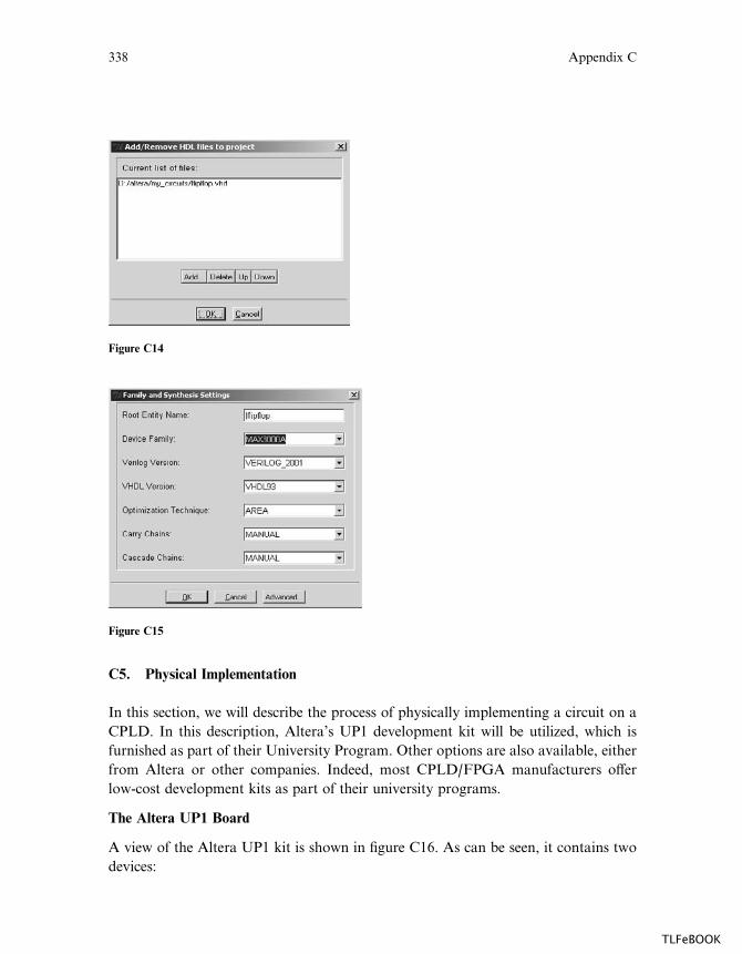
C5. Physical Implementation
In this section, we will describe the process of physically implementing a circuit on a
CPLD. In this description, Altera’s UP1 development kit will be utilized, which is
furnished as part of their University Program. Other options are also available, either
from Altera or other companies. Indeed, most CPLD/FPGA manufacturers o¤er
low-cost development kits as part of their university programs.
The Altera UP1 Board
A view of the Altera UP1 kit is shown in figure C16. As can be seen, it contains two
devices:
Figure C14
Figure C15
338 Appendix C
TLFeBOOK

� EPM7128SLC84-7 (from the MAX7000S family): This is a CPLD (appendix A) in
an 84-pin package. It contains 128 macrocells, each having a PAL-type architecture
and one flip-flop.
� EPF10K20RC240-4 (from the FLEK10K family): This is an FPGA (appendix A)
in a 240-pin package. It consists of 1,152 LEs (logic elements), each with a 4-bit LUT
(lookup table) and one flip-flop.
For testing the CPLD, the board contains eight LEDs (light emitting diodes), two
SSDs (seven-segment displays), and two eight-bit dip switches (figure C16). And, for
testing the FPGA, 2 more SSDs and another eight-bit dip switch. The LEDs and the
segments of the SSDs use negative logic, thus being turned on when 0 V is applied.
The switches, on the other hand, provide 5 V signals when moved up or 0 V when
moved down.
The LEDs and switches are not connected to any of the chip pins, so they can be
freely wired to the devices to satisfy any particular setup. However, the segments of
the SSDs are already connected, thus requiring the implemented circuit to have spe-
cific pin assignments. In the case of the CPLD, the pins to which the SSDs are con-
nected are those listed in figure C17.
The board also contains a 25.175 MHz clock, which is connected to the devices
(the global clock pin of the CPLD is pin 83).
Figure C16
Altera MaxPlus IIþAdvanced Synthesis Software Tutorial 339
TLFeBOOK

The complete specifications of the board are available at www.altera.com/
literature/univ/upds.pdf.
Setting up the UP1 Board
� In the description presented below, the CPLD (EPM7128SLC84-7) will be used as
the target device. Therefore, the jumpers in the TDO, TDI, DEVICE, and BOARD
columns (see figure C16, right above the EPM7128S device) should all be installed in
the upper position (that is, between the upper two pins, C1 and C2, of each column
of pins, as indicated in the table of figure C18).
� Connect the ByteBlaster cable provided with the kit between the board and the
parallel port of the PC.
� Connect the DC supply (9 V) to the board. Notice that the Power LED and two
SSDs are lit.
Figure C17
Table 2. JTAG Jumper Settings
Desired Action TDI TDO DEVICE BOARD
Program EPM7128S device only
C1 & C2 C1 & C2 C1 & C2 C1 & C2
Configure FLEX 10k device only
C2 & C3 C2 & C3 C1 & C2 C1 & C2
Program/configure both devices
C2 & C3 C1 & C2 C2 & C3 C1 & C2
Connect multiple boards together
C2 & C3 OPEN C2 & C3 C2 & C3
Figure C18
340 Appendix C
TLFeBOOK
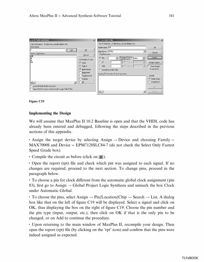
Implementing the Design
We will assume that MaxPlus II 10.2 Baseline is open and that the VHDL code has
already been entered and debugged, following the steps described in the previous
sections of this appendix.
� Assign the target device by selecting Assign ! Device and choosing Family ¼MAX7000S and Device ¼ EPM7128SLC84-7 (do not check the Select Only Fastest
Speed Grade box).
� Compile the circuit as before (click on ).
� Open the report (rpt) file and check which pin was assigned to each signal. If no
changes are required, proceed to the next section. To change pins, proceed in the
paragraph below.
� To choose a pin for clock di¤erent from the automatic global clock assignment (pin
83), first go to Assign ! Global Project Logic Synthesis and unmark the box Clock
under Automatic Global.
� To choose the pins, select Assign ! Pin/Location/Chip ! Search ! List. A dialog
box like that on the left of figure C19 will be displayed. Select a signal and click on
OK, thus displaying the box on the right of figure C19. Choose the pin number and
the pin type (input, output, etc.), then click on OK if that is the only pin to be
changed, or on Add to continue the procedure.
� Upon returning to the main window of MaxPlus II, recompile your design. Then
open the report (rpt) file (by clicking on the ‘rpt’ icon) and confirm that the pins were
indeed assigned as expected.
Figure C19
Altera MaxPlus IIþAdvanced Synthesis Software Tutorial 341
TLFeBOOK

Downloading the Design
Your design is now ready to be downloaded onto the chip.
� Double-click on the pof (program object file) icon (shown at the end of compila-
tion, figure C3). A box like that of figure C20 will be displayed.
� Select, in the main menu, Options ! Hardware Setup ! ByteBlaster(MV), then
click on OK.
� Finally, in the screen of figure C20, click on Program to program the device. After
a few moments, the chip will be ready to be physically tested and/or used.
Figure C20
342 Appendix C
TLFeBOOK
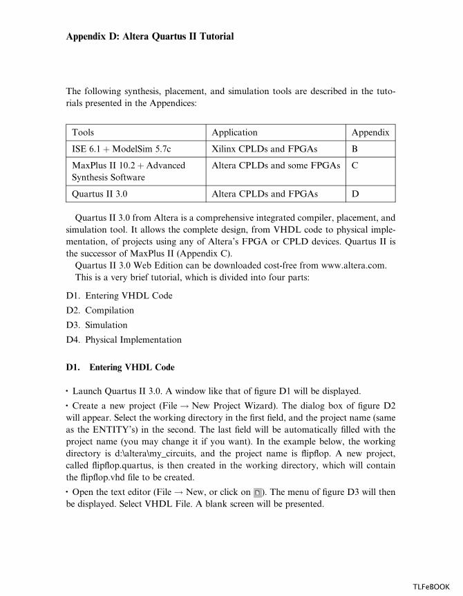
Appendix D: Altera Quartus II Tutorial
The following synthesis, placement, and simulation tools are described in the tuto-
rials presented in the Appendices:
Tools Application Appendix
ISE 6.1þModelSim 5.7c Xilinx CPLDs and FPGAs B
MaxPlus II 10.2þAdvanced
Synthesis Software
Altera CPLDs and some FPGAs C
Quartus II 3.0 Altera CPLDs and FPGAs D
Quartus II 3.0 from Altera is a comprehensive integrated compiler, placement, and
simulation tool. It allows the complete design, from VHDL code to physical imple-
mentation, of projects using any of Altera’s FPGA or CPLD devices. Quartus II is
the successor of MaxPlus II (Appendix C).
Quartus II 3.0 Web Edition can be downloaded cost-free from www.altera.com.
This is a very brief tutorial, which is divided into four parts:
D1. Entering VHDL Code
D2. Compilation
D3. Simulation
D4. Physical Implementation
D1. Entering VHDL Code
� Launch Quartus II 3.0. A window like that of figure D1 will be displayed.
� Create a new project (File ! New Project Wizard). The dialog box of figure D2
will appear. Select the working directory in the first field, and the project name (same
as the ENTITY’s) in the second. The last field will be automatically filled with the
project name (you may change it if you want). In the example below, the working
directory is d:\altera\my_circuits, and the project name is flipflop. A new project,
called flipflop.quartus, is then created in the working directory, which will contain
the flipflop.vhd file to be created.
� Open the text editor (File ! New, or click on ). The menu of figure D3 will then
be displayed. Select VHDL File. A blank screen will be presented.
TLFeBOOK
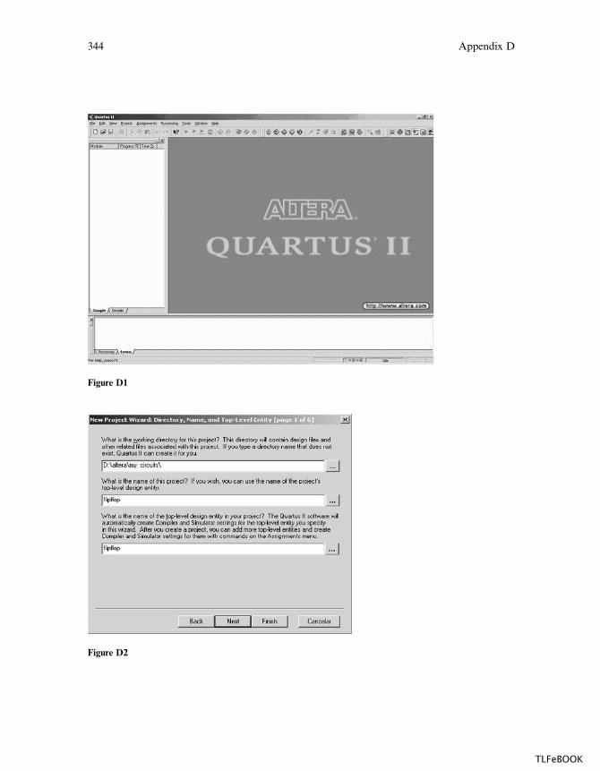
Figure D1
Figure D2
344 Appendix D
TLFeBOOK
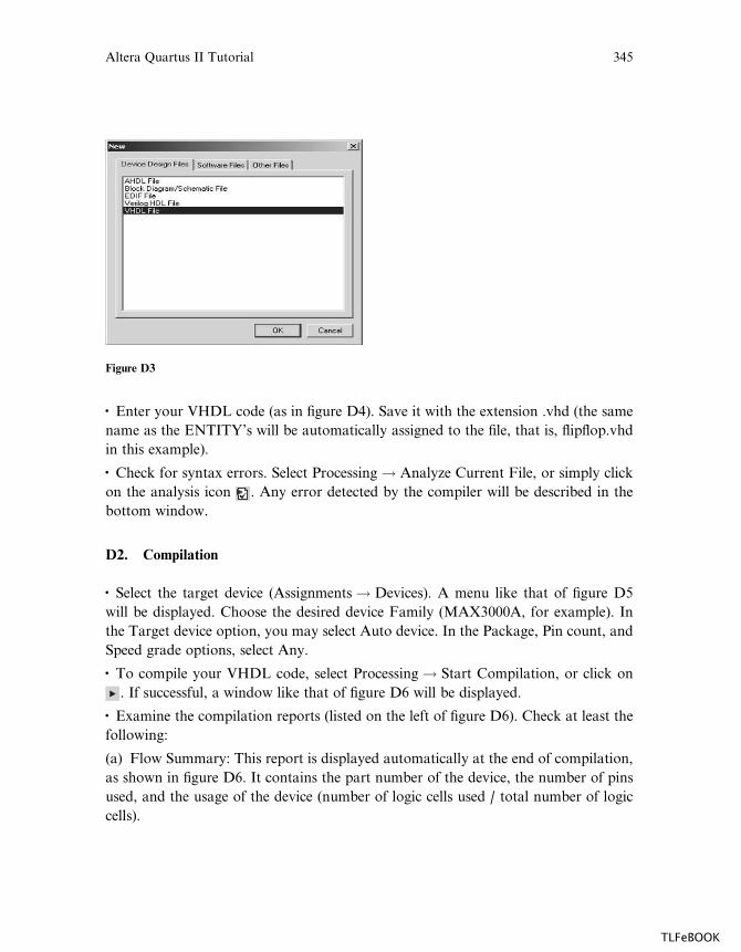
� Enter your VHDL code (as in figure D4). Save it with the extension .vhd (the same
name as the ENTITY’s will be automatically assigned to the file, that is, flipflop.vhd
in this example).
� Check for syntax errors. Select Processing ! Analyze Current File, or simply click
on the analysis icon . Any error detected by the compiler will be described in the
bottom window.
D2. Compilation
� Select the target device (Assignments ! Devices). A menu like that of figure D5
will be displayed. Choose the desired device Family (MAX3000A, for example). In
the Target device option, you may select Auto device. In the Package, Pin count, and
Speed grade options, select Any.
� To compile your VHDL code, select Processing ! Start Compilation, or click on
. If successful, a window like that of figure D6 will be displayed.
� Examine the compilation reports (listed on the left of figure D6). Check at least the
following:
(a) Flow Summary: This report is displayed automatically at the end of compilation,
as shown in figure D6. It contains the part number of the device, the number of pins
used, and the usage of the device (number of logic cells used / total number of logic
cells).
Figure D3
Altera Quartus II Tutorial 345
TLFeBOOK
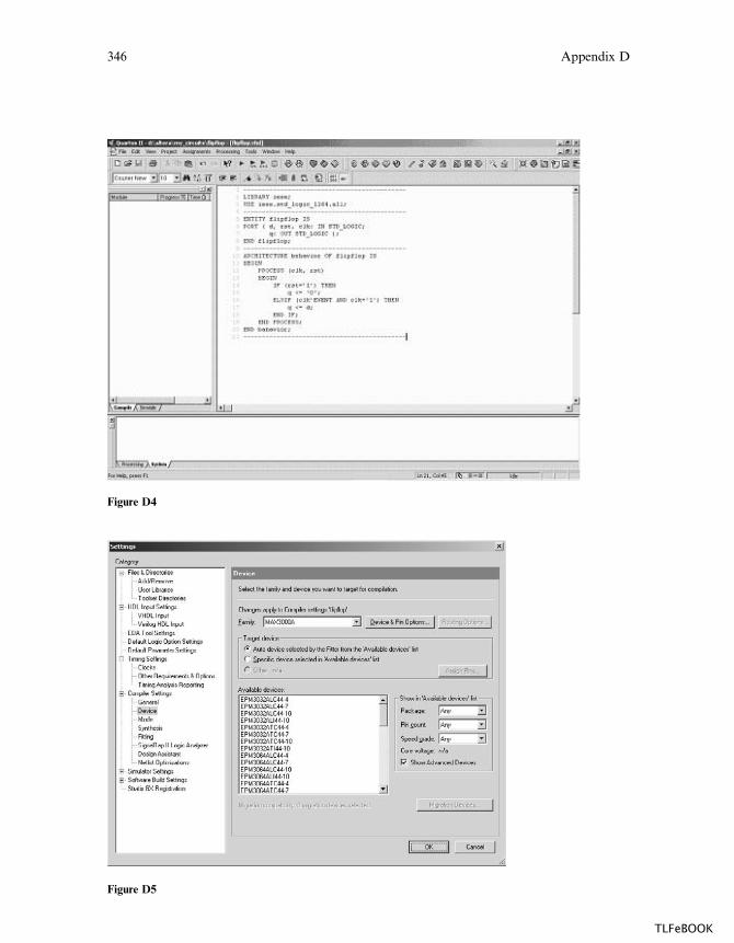
Figure D4
Figure D5
346 Appendix D
TLFeBOOK
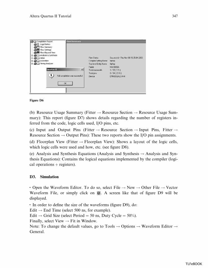
(b) Resource Usage Summary (Fitter ! Resource Section ! Resource Usage Sum-
mary): This report (figure D7) shows details regarding the number of registers in-
ferred from the code, logic cells used, I/O pins, etc.
(c) Input and Output Pins (Fitter ! Resource Section ! Input Pins, Fitter !Resource Section ! Output Pins): These two reports show the I/O pin assignments.
(d) Floorplan View (Fitter ! Floorplan View): Shows a layout of the logic cells,
which logic cells were used and how, etc. (see figure D8).
(e) Analysis and Synthesis Equations (Analysis and Synthesis ! Analysis and Syn-
thesis Equations): Contains the logical equations implemented by the compiler (logi-
cal operationsþ registers).
D3. Simulation
� Open the Waveform Editor. To do so, select File ! New ! Other File ! Vector
Waveform File, or simply click on . A screen like that of figure D9 will be
displayed.
� In order to define the size of the waveforms (figure D9), do:
Edit ! End Time (select 500 ns, for example).
Edit ! Grid Size (select Period ¼ 50 ns, Duty Cycle ¼ 50%).
Finally, select View ! Fit in Window.
Note: To change the default values, go to Tools ! Options ! Waveform Editor !General.
Figure D6
Altera Quartus II Tutorial 347
TLFeBOOK
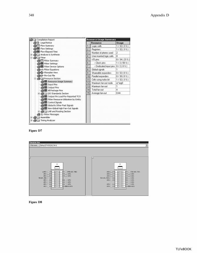
Figure D7
Figure D8
348 Appendix D
TLFeBOOK
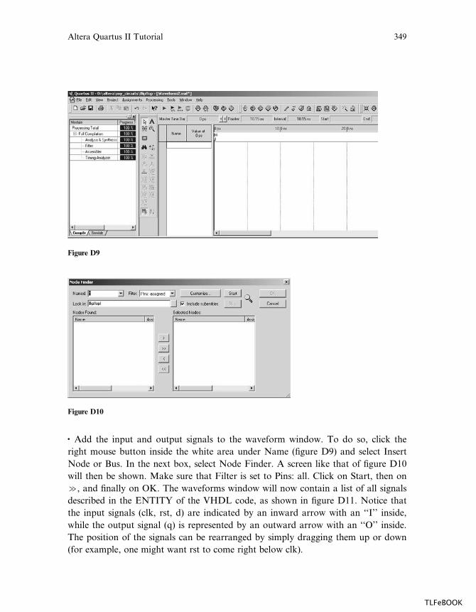
� Add the input and output signals to the waveform window. To do so, click the
right mouse button inside the white area under Name (figure D9) and select Insert
Node or Bus. In the next box, select Node Finder. A screen like that of figure D10
will then be shown. Make sure that Filter is set to Pins: all. Click on Start, then on
X, and finally on OK. The waveforms window will now contain a list of all signals
described in the ENTITY of the VHDL code, as shown in figure D11. Notice that
the input signals (clk, rst, d) are indicated by an inward arrow with an ‘‘I’’ inside,
while the output signal (q) is represented by an outward arrow with an ‘‘O’’ inside.
The position of the signals can be rearranged by simply dragging them up or down
(for example, one might want rst to come right below clk).
Figure D9
Figure D10
Altera Quartus II Tutorial 349
TLFeBOOK
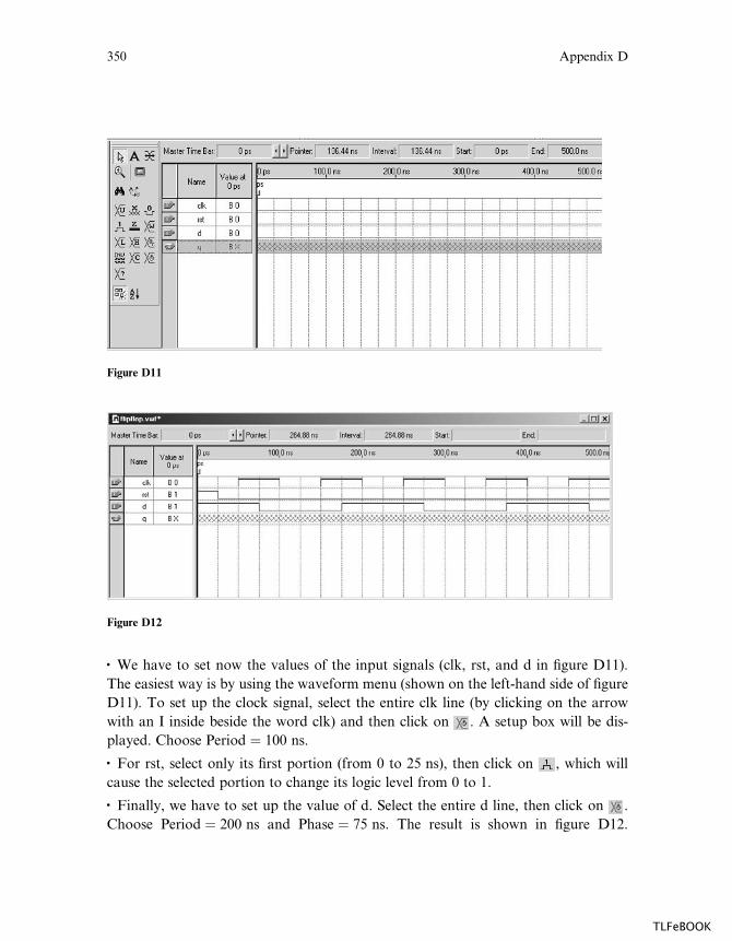
� We have to set now the values of the input signals (clk, rst, and d in figure D11).
The easiest way is by using the waveform menu (shown on the left-hand side of figure
D11). To set up the clock signal, select the entire clk line (by clicking on the arrow
with an I inside beside the word clk) and then click on . A setup box will be dis-
played. Choose Period ¼ 100 ns.
� For rst, select only its first portion (from 0 to 25 ns), then click on , which will
cause the selected portion to change its logic level from 0 to 1.
� Finally, we have to set up the value of d. Select the entire d line, then click on .
Choose Period ¼ 200 ns and Phase ¼ 75 ns. The result is shown in figure D12.
Figure D11
Figure D12
350 Appendix D
TLFeBOOK

Notice that q is not available yet, for it will be determined by the simulator. Save the
waveform as flipflop.vwf.
� The system is now ready for simulation. Select Processing ! Start Simulation, or
just click on . The result should look like that in figure D13.
D4. Physical Implementation
� Development kit: To perform the physical implementation, we will assume that an
Altera UP1 (or UP2) kit is available (this development kit was described in section
C5 of appendix C). The kit must be connected to the parallel port of the PC by
means of a ByteBlaster cable (provided with the kit).
� Device selection: The kit (Altera UP1 or UP2) contains two devices,
EPM7128SLC84-7 (a CPLD from the MAX7000S family) and EPF10K70RC240-4
(an FPGA from the FLEX10K family). Therefore, in the Assignments ! Devices
step of section D2, one of these two devices must be selected.
� Changing pin assignments: The I/O pins are automatically assigned during compi-
lation. However, if desired, the assignments can be changed. Select Assignments !Assign Pins, which will cause the window of figure D14 to be opened. Say that we
want rst to be connected to pin 4, for example. Select pin 4, then click on , which
will open the window of figure D10. Click on Start, select rst on the left column, then
click on > and OK. Upon returning to the window of figure D14, click on Add.
Repeat this process for any other changes of pin assignments.
Figure D13
Altera Quartus II Tutorial 351
TLFeBOOK
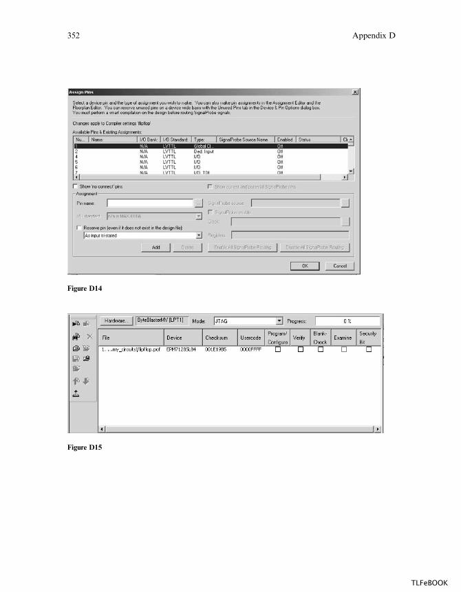
Figure D14
Figure D15
352 Appendix D
TLFeBOOK

� Setting up the Programmer: To download the program to the kit (device), first
select Tools ! Programmer, or click on . The window of figure D15 will be
shown. In the Hardware option, ByteBlasterMV (LPT1) should appear. If not, click
on Hardware, then on Select Hardware, select ByteBlasterMV, and finally click on
Add Hardware. Returning to the window of figure D15, in the File column verify
that the design file, with the extension .pof (program object file), is present. Then
check the box under Program/Configure.
� Programming the device: Finally, the device can be programmed. Just select
Processing ! Start Programming. After a few moments, programming will be con-
cluded and the chip ready to be physically tested and/or used.
Altera Quartus II Tutorial 353
TLFeBOOK

TLFeBOOK
Appendix E: VHDL Reserved Words
From VHDL 87:
ABS
ACCESS
AFTER
ALIAS
ALL
AND
ARCHITECTURE
ARRAY
ASSERT
ATTRIBUTE
BEGIN
BLOCK
BODY
BUFFER
BUS
CASE
COMPONENT
CONFIGURATION
CONSTANT
DISCONNECT
DOWNTO
ELSE
ELSIF
END
ENTITY
EXIT
FILE
FOR
FUNCTION
GENERATE
GENERIC
GUARDED
IF
IN
INOUT
IS
LABEL
LIBRARY
LINKAGE
LOOP
MAP
MOD
NAND
NEW
NEXT
NOR
NOT
NULL
OF
ON
OPEN
OR
OTHERS
OUT
PACKAGE
PORT
PROCEDURE
PROCESS
RANGE
RECORD
REGISTER
REM
REPORT
RETURN
SELECT
SEVERITY
SIGNAL
SUBTYPE
THEN
TO
TRANSPORT
TYPE
UNITS
UNTIL
USE
VARIABLE
WAIT
WHEN
WHILE
WITH
XOR
From VHDL 93:
GROUP
IMPURE
INERTIAL
LITERAL
POSTPONED
PURE
REJECT
ROL
ROR
SHARED
SLA
SLL
SRA
SRL
UNAFFECTED
XNOR
TLFeBOOK

TLFeBOOK
Bibliography
Armstrong J. R. and F. G. Gray, VHDL Design Representation and Synthesis, Englewood Cli¤s, NJ:Prentice Hall, 2nd Edition, 2000.
Bhasker J., VHDL Primer, Englewood Cli¤s, NJ: Prentice Hall, 3rd Edition, 1999.
Chang K. C., Digital Systems Design with VHDL and Synthesis—An Integrated Approach, Los Alamitos,CA: IEEE Computer Society Press, 1999.
Hamblen J. and M. Furman, Rapid Prototyping of Digital Systems, Boston: Kluwer Academic Publisher,2nd Edition, 2001.
Naylor D. and S. Jones, VHDL: A Logic Synthesis Approach, London: Chapman & Hall, 1997.
Navabi Z., VHDL Analysis and Modeling of Digital Systems, New York: McGraw-Hill, 1993.
Pellerin D. and D. Taylor, VHDL Made Easy, Englewood Cli¤s, NJ: Prentice Hall, 1997.
Perry D. L., VHDL, New York: McGraw-Hill, 2nd Edition, 1994.
Yalamanchili S., Introductory VHDL from Simulation to Synthesis, Englewood Cli¤s, NJ: Prentice Hall,2001.
Yalamanchili S., VHDL Starter’s Guide, Englewood Cli¤s, NJ: Prentice Hall, 1998.
TLFeBOOK

TLFeBOOK
Index
þ Addition operator, 49, 54, 60, 195¼> Assignment operator for OTHERS, 47, 60<¼ Assignment operator for SIGNAL, 47, 60:¼ Assignment operator for VARIABLE,
CONSTANT, or GENERIC, 47, 60= Division operator, 49, 60¼ Equal-to operator, 49, 60�� Exponentiation operator, 49, 60> Greater-than operator, 49, 60>¼ Greater-than-or-equal-to operator, 49, 60< Less-than operator, 49, 60<¼ Less-than-or-equal-to operator, 49, 60� Multiplication operator, 49, 60=¼ Not-equal-to operator, 49, 60� Subtraction operator, 49, 60
ABS operator, 49, 60Absolute value operator, 49, 60Accumulate (multiply-and-), 285–288, 290, 292,
295, 299Actel FPGAs, 315ACTIVE attribute, 52, 61Adder circuits, 5–7, 42–43, 106–109, 194–198Basic adder, 42–43Carry-look-ahead adder, 196–198Carry-ripple adder, 106–109, 194–196Full-adder, 5–7, 279, 282–283MAC (multiply-and-accumulate), 285–288, 290,292, 295, 299Overflow, 286
Addition operator, 49, 54, 60, 195Advanced Synthesis Software, 329, 336–338AFTER clause, 28AlteraAdvanced Synthesis Software, 329, 336–338CPLDs, 312MaxPlus II software, 5, 20, 329–342Quartus II software, 4–5, 20, 343–353
ALU, 75–78, 247–251AND operator, 36–37, 41–42, 48, 60Antifuse, 306, 313, 315Application Specific Integrated Circuit. See ASICARCHITECTUREDescription, 17Introductory examples, 6, 17–22Usage, 13–14
Arithmetic logic unit. See ALUArithmetic operators, 48–49, 60ARRAY, 30–33, 39Array indexes, 51ASIC, 3, 4, 6, 211, 293ASSERT statement, 270–271Assignment operators, 47–48, 60ATTRIBUTE statement, 52–53Attributes, 50–53, 61
Data attributes, 51, 61Signal attributes, 52, 61Summary, 61User-defined attributes, 52–53
Barrel/vector shifter circuits, 80–81, 109–111,187–190
Base type, 29–30BEGIN keywordwith ARCHITECTURE, 17with BLOCK, 81–83with FUNCTION, 253with PROCEDURE, 265with PROCESS, 91Behavioral description, 91Binary versus one-hot and two-hot encoding,181–182
Binary-to-Gray-code converter, 87BIT. See Data typesBIT_VECTOR. See Data typesBIT versus BIT_VECTOR, 41–42BLOCK statementGuarded, 83–84Simple, 81–83BODY. See PACKAGE BODYBOOLEAN. See Data typesBu¤er circuit, 73BUFFER mode, 16, 37–138, 140, 143, 145, 152,154, 157
Carry-look-ahead adder circuit. See Adder circuitsCarry-ripple adder circuits. See Adder circuitsCASE statement, 91, 100–104CASE versus IF, 112–113CASE versus WHEN, 113–114Combinational versus sequential circuits, 65–66Comparator circuits, 191–194Comparison operators, 49, 60Complex programmable logic devices. See CPLDsCOMPONENT, 234, 236–244Concatenation operators, 50, 60Concurrent code, 65–84Concurrent statementsBLOCK, 65, 81–84GENERATE, 65, 78–81, 195, 197–198WHEN, 65, 69–78WHEN versus CASE, 113–114Concurrent versus sequential code, 65–67CONFIGURATION statement, 72CONSTANT, 31, 47, 129–131, 174–176, 220–221,234–235, 270
Controller circuit for tra‰c light, 174–178, 186Controller circuit for vending machine, 202–208,226–227
Conv_integer function, 25, 37, 43, 255, 258–259
TLFeBOOK
Conv_signed function, 25, 37Conv_std_logic_vector function, 25, 38Conv_unsigned function, 25, 37Conversion functions. See Data conversion
functionsCount ones circuits, 130–133Counter circuits, 94–96, 99–100, 102–104, 144–
146, 155, 164–166, 272CPLDs, 3–4, 305–306, 311–313, 317, 338–340
Data attributes, 51, 61Data conversion functions, 25, 37–38Data objects. See ObjectsData types, 25–43ARRAY, 30–33, 39BIT, 16–17, 21–22, 25–26, 39, 48–49, 54–55BIT_VECTOR, 25–26, 28–30, 39, 48–49, 54–55BIT versus BIT_VECTOR, 41–42BOOLEAN, 25, 27–28, 30, 39, 204, 235–237,254–257Enumerated data types, 28–29, 39, 51, 53, 61, 70,101, 160, 162, 164, 204INTEGER, 25, 27–28, 30, 35, 37–39, 48–49NATURAL, 27, 29–30, 34–35, 262, 300Physical data types, 27Port array, 33–34REAL, 25, 27, 39RECORD, 35, 39SIGNED, 25, 27, 30, 35–39, 42–43, 48, 191, 285,291, 297STD_LOGIC, 25–27, 39STD_LOGIC_VECTOR, 25–27, 39STD_ULOGIC, 25–27, 39STD_ULOGIC_VECTOR, 26, 39SUBTYPE, 29–30, 39, 80, 226UNSIGNED, 25, 27, 30, 35–39, 48, 191, 263–265User-defined, 28–29, 34, 39, 299
Decoder circuits, 55–57, 62–63, 156Delay circuit, 152DFF, 18–22, 83–84, 92–93, 99, 101–102, 125–127,
137–138, 142–143, 152–155, 157–158, 254–255Digital filter circuit, 289–294, 303Divider circuit, fixed-point, 198–202Division operator, 49, 60Don’t care, 26D-type flip-flop. See DFF
EDIF, 329, 336, 337EEPROM, 306, 309, 312–313ELSEwith WHEN, 69with IF, 94
ELSIF, 94Encoder circuit, 73–75END keywordwith ARCHITECTURE, 17with BLOCK, 81–83with CASE, 100with FUNCTION, 253with GENERATE, 78–79with IF, 94with LOOP, 105with PROCEDURE, 265with PROCESS, 91ENTITYDescription, 15–17Introductory examples, 6, 17–22Usage, 13–14Enum_encoding attribute, 53Enumerated data types. See Data typesEPROM, 308–309Equal-to operator, 49, 60Error message. See ASSERT statementEVENT attribute, 52, 61Event counter circuit, 121Exclusive-NOR operator, 48, 60Exclusive-OR operator, 48, 60EXIT statement, 105–106, 111–112Exponentiation operator, 49, 60
Field Programmable Gate Arrays. See FPGAsFinite State Machine. See FSMFIR filter. See Digital filter circuitFlip-flop. See DFFFOR statementwith GENERATE, 78–81with LOOP, 105–112with WAIT, 98–99FPGAs, 3–4, 305–306, 311–315, 317, 338–339Frequency divider circuit, 122, 138–140FSM, 159–182, 202–208, 213–218Full-adder. See Adder circuitsFUNCTION, 253–265Arithmetic shift function, 261–262Convert-to-integer function, 37, 43, 255, 258–259Definition and syntax, 253–254Function location, 256–258Multiplication function, 263–265Multiplier function, 263–265Overloaded ‘‘þ’’ operator function, 260–261Positive_edge function, 254–258FUNCTION versus PROCEDURE, 270
GAL devices, 305–306, 309–312GENERATE statement, 65, 78–81, 195, 197–198GENERIC MAP, 244–247
360 Index
TLFeBOOK

GENERIC statement, 54–60, 97, 108–109, 117,191–195, 201, 221, 223, 225
Gray code, 87Greater-than operator, 49, 60Greater-than-or-equal-to operator, 49, 60GUARDED BLOCK, 83–84
Hexadecimal, 28, 43HIGH attribute, 51, 61High-impedance, 26, 73
IEEE library, 13–15, 25–27, 35–38IEEE standards for VHDL, 25IF statement, 91, 94–97IF versus CASE, 112–113IF-GENERATE, 78–79IN mode, 16–17Inferred registers, number of, 140–151INOUT mode, 16, 225INTEGER. See Data typesIntensity encoder circuit, 124IS keywordwith ARCHITECTURE, 17with ATTRIBUTE, 53with CASE, 100with COMPONENT, 237with ENTITY, 16with FUNCTION, 253with PACKAGE, 234with PACKAGE BODY, 234with PROCEDURE, 265with SUBTYPE, 29–30with TYPE, 28–29
ISE software, 4–5, 20, 317–327
Keypad debouncer/encoder circuit, 184–186
LAST_ACTIVE attribute, 52LAST_EVENT attribute, 52LAST_VALUE attribute, 52Latch, 83–84, 119, 121 (see also DFF)Leading zeros counter circuit, 111–112LEFT attribute, 51, 61LEFTOF attribute, 51, 61LENGTH attribute, 51, 61Less-than operator, 49, 60Less-than-or-equal-to operator, 49, 60LibraryDeclaration, 13–15IEEE library, 13, 15, 25–27, 35–38Introductory examples, 18–22Standard library, 13, 15, 25Std_logic_1164 package, 13, 15, 25–27Std_ulogic_1164 package, 25–27
Std_logic_arith package, 15, 25, 27, 35–38, 42–43, 191, 263, 285, 287, 291, 296, 299Std_logic_signed package, 15, 25, 27, 36, 38, 48Std_logic_unsigned package, 15, 25, 27, 36, 38,48Work library, 13, 15Logic systemsBinary (std library), 25STD_LOGIC, 25–27STD_ULOGIC, 25–27Logical operators, 48, 60LOOP statement, 91, 105–112LOW attribute, 51, 61
MAC circuits, 285–288, 290, 292, 295, 299MAPGENERIC MAP, 244–247PORT MAP, 237, 241, 244–245, 251, 277–279,281–284
MaxPlus II software, 5, 20, 329–342Min_max procedure, 267–270MOD operator, 49, 60ModeBUFFER, 16, 137–138, 140, 143, 145, 152, 154,157IN, 16–22INOUT, 16, 225, 266OUT, 16–22ModelSim software, 5, 20, 317, 325–326Modulus operator, 49, 60Multiplexer circuits, 68, 70–72, 85, 134–137Multiplication operator, 49, 60Multiplier circuits, 263–265, 275–285Multiply-and-accumulate circuit. See MACcircuits
Multivalued logic systemsSTD_LOGIC, 25–27STD_ULOGIC, 25–27MUX. See Multiplexer circuits
NAND operator, 48, 60NATURAL. See Data typesNeural networks, 294–301, 303NEXT statement, 105–106NOR operator, 48, 60NOT operator, 48, 60Not-equal-to operator, 49, 60NULL statement, 101–102, 104, 113–114Number of registers inferred, 140–151Numeric data types. See Data types
ObjectsCONSTANT, 31, 47, 129–131, 174–176, 220–221, 234–235, 270
Index 361
TLFeBOOK
Objects (cont.)SIGNAL, 19, 21–22, 129–132SIGNAL versus VARIABLE, 133–140VARIABLE, 129–133
ON keyword, 98–99One-hot encoding, 181–182Operator overloading, 53–54, 260–261OperatorsArithmetic, 48–49, 60Assignment, 47–48, 60Comparison, 49, 60Concatenation, 50, 60Logical, 48, 60Shift, 49–50, 60Summary, 60
OR operator, 48, 60OTHERS clause, 40, 47–48, 69–73, 94, 101–102,
112–114OUT mode, 16–22Overloading, 53–54, 260–261
PACKAGEDescription, 13–14, 93, 133, 233–236, 256,266–270Examples, 34–35, 235–236, 239, 241–244, 257–260, 263–264, 268–270, 275–284, 287, 299
PACKAGE BODY, 234–236, 256–260, 269–270,287
PAL devices, 305–308, 339PALCE devices, 305Parity detector circuit, 57–59, 123Parity generator circuit, 59–60Physical data types, 27PLA devices, 305–306, 308–309, 312Playing with a seven-segment display, 212–216,
228PLDsCPLD, 3–4, 305–306, 311–313, 317, 338–340FPGA, 3–4, 305–306, 311–315, 317, 338–339GAL, 305–306, 309–312PAL, 305–308, 339PLA, 305–306, 308–309, 312
PORTIntroductory examples, 5–6, 18–22Modes. See Mode
Port array, 33–35PORT MAP, 237, 241, 244, 251, 277–279,
281–284Pre-defined data attributes, 51, 61Pre-defined data types, 25–28, 39Pre-defined operators, 47–50, 60Pre-defined signal attributes, 52, 61Priority encoder circuit, 85, 121–122PROCEDURE, 13–14, 91, 94, 105, 113, 130–133,
233–235, 265–270
PROCEDURE versus FUNCTION, 270PROCESSDescription, 91–94Introductory examples, 18–22, 56–60, 92–120Programmable array logic. See PALProgrammable logic array. See PLAProgrammable logic devices. See PLDs
Quartus II software, 4–5, 20, 343–353QUIET attribute, 52
RAM circuits, 116–118, 221–225Random access memory. See RAM circuitsRANGE attribute, 28–30, 34–35, 37, 51, 61Read-only memory. See ROM circuitsREAL. See Data typesRECORD, 35, 39Registers. See DFFRegisters inferred, number of, 140–151Relational operators. See OperatorsREM operator, 49, 60Remainder operator, 49, 60REPORT statement, 271Reserved words, 355Resolved data type, 26–27, 39REVERSE_RANGE attribute, 51, 61RIGHT attribute, 51, 61, 262ROL operator, 50, 60ROM circuits, 44, 220–221ROR operator, 50, 60Rotate left logic operator, 50, 60Rotate right logic operator, 50, 60RTL, 4
SELECT statement, 67, 69–73, 113Sequential code, 65, 91–121Sequential statementsCASE, 91, 100–104, 112–114IF, 91, 94–97, 112–113LOOP, 91, 105–112WAIT, 91, 97–100Serial data receiver circuit, 208–211, 227Seven-segment display, 212–216, 228Shift left arithmetic operator, 50, 60Shift left logic operator, 49–50, 60Shift operators, 49–50, 60Shift register circuits, 96–97, 121, 146–151Shift right arithmetic operator, 50, 60Shift right logic operator, 49–50, 60SIGNAL, 19, 21–22, 129–132Signal attributes, 52, 61Signal generator circuits, 178–181, 183–184, 186,
217–220SIGNAL versus VARIABLE, 133–140SIGNED. See Data types
362 Index
TLFeBOOK
SLA operator, 50, 60SLL operator, 49–50, 60Speed monitor circuit, 228–229SRA operator, 50, 60SRL operator, 49–50, 60STD_LOGIC, 25–27, 39STD_LOGIC_VECTOR, 25–27, 39STD_ULOGIC, 25–27, 39STD_ULOGIC_VECTOR, 26–27, 39Stop-watch circuit, 252String detector circuit, 172–174Subtype, 29–30, 39
Timer circuits, 123Tra‰c light controller circuit, 174–178, 186Tri-state bu¤er circuit, 73Two-hot encoding, 181–182Types. See Data types
UNAFFECTED statement, 69–70, 101, 113–114Unresolved data type, 27, 39UNSIGNED. See Data typesUNTIL, 52, 98–100USE clause, 13, 15User-defined attributes, 52–53User-defined data types, 28–29, 34, 39, 299
VARIABLE, 129–133VARIABLE versus SIGNAL, 133–140Vending machine controller circuit, 202–208,
226–227VHDL acronym, 3VHDL reserved words, 355
WAIT statement, 91, 97–100WHEN statement, 65, 69–78WHEN versus CASE, 113–114WHILE statement, 105–106WITH, 67, 69–73, 113Work library, 13, 15
XilinxCPLDs, 312FPGAs, 314ISE software, 4–5, 20, 317–327
XNOR operator, 48, 60XOR operator, 48, 60
‘‘Z’’ logic state, 26–27, 39, 73
Index 363
TLFeBOOK

TLFeBOOK