carbon aero gel (cag) super-capacitor a fractional order
TRANSCRIPT

Carbon Aero Gel (CAG) Super-Capacitor a Fractional Order Element
in reality and why?
Shantanu DasScientist H+, RCSDS BARC Mumbai,
Senior Research Professor Dept. of Phys, Jadavpur Univ (JU),Adjunct Professor DIAT-Pune
UGC-Visiting Fellow Dept. of Appl. Math Calcutta [email protected]
http://scholar.google.co.uk/citations?user=9ix9YS8AAAAJ&hl=enwww.shantanudaslecture.com
VECC-Kolkata12 May 2015

Research and development team & Funding organizations
CMET ThrissurDr. N. C. Pramanik (Scientist Aerogel Div. CMET); [email protected]
IIT BombayProf. Vivek Agarwal (Dept. of EE) ; [email protected]
VNIT NagpurProf. Mohan. V. Aware (Dept. of EE); [email protected]
NIT RaipurProf. Subhojit Ghosh (Dept. of EE) ; [email protected]
ECILSri. M. R. K. Naidu (Head Corporate R & D) ; [email protected]
Funding Organizations: DeitY, DST, BRNS

Keltron
ECIL
Tata Motors,
SPEL Technologies
Mahindra Reva Electric Vehicle Pvt. Ltd.
Chheda Electrical & Electronics Pvt. Ltd.
Power Systems Ltd. Aartech Solution Ltd.
SAMEER
CSIR-CMERI Durgapur
Probable end users

Various of CAG super capacitors cells made
Values of the CAG super capacitors are 1 Farad to 50 Farad 2.5V made by CAG electrodes
BRNS Sanction No.2009/34/31/BRNS dated 22.10.2009 CMET & BARC Joint Project

Parameter Imported Super capacitor
In-house made CAG super-capacitor
Electrode size (mm) 10 X 180 10 X 110Material Carbon Foam
Graphine, Gold Foam, Activated Carbon
Carbon Aero gel
Capacitance 1.00 Farad 1.00 FaradTolerance +/-20 % +/- 10 %Operating Voltage 0.5-2.50 Volts 0.5- 2.50 VoltsEquivalent Series Resistance ESR
0.4-0.6 Ohms 0.35-0.45 Ohms
Comparing imported & in house 1Farad super-capacitors
CAG super capacitors Requires 0.6 times electrode material compared toimported ones
BRNS Sanction No.2009/34/31/BRNS dated 22.10.2009 CMET & BARC Joint Project

From Organic Gel RF Gel i.e. Resorcinol Phenol sol-gel polymer is made.
Then at inert atmosphere pyrolysis is done to get Carbon Aero gel
The process from RF Gel to Farad Capacitors
BRNS Sanction No.2009/34/31/BRNS dated 22.10.2009 CMET & BARC Joint Project
Electrolyte : TEATFBTetra Ethyl Ammonium Tetra Fluorite Borate

2.1 cm
1.2 cmdia
2.4 cmdia
4.1 cm
Size-1; 5 F-20 F Size-2; 1F-3 F
Packing size for CAG Capacitor
Packed in two sizesBRNS Sanction No.2009/34/31/BRNS dated 22.10.2009 CMET & BARC Joint Project

The circuit for bicycle lighting system
6V Generator
Tail Lamp
1N4001
SC 1F
8.2M
6
7
0.1uF1 5
1K
2
0.1uF
390K
4 83
0.1uF
1K2N3906Timer IC
555
TailLight
BRNS Sanction No.2009/34/31/BRNS dated 22.10.2009 CMET & BARC Joint Project
The tail light flashes even while cycle stops

The circuit driving toy car with geared wheel
1N4007 1N4007
27 ohm
100 ohm
100 ohm
LED
27 ohmSC 18 F
Motor
SW SW
5V DC
BRNS Sanction No.2009/34/31/BRNS dated 22.10.2009 CMET & BARC Joint Project

The circuit LED backup
1N4007
1N4007
LED-1
LED-2SC 18F
100 ohm
100 ohm
100 ohm
SW
SW5V DC
BRNS Sanction No.2009/34/31/BRNS dated 22.10.2009 CMET & BARC Joint Project

Photograph of CAG supercapacitor powered fast charging Emergency Lighthaving two 25F/ 2.5 V, 1-3W Power LED, which takes ~90 second for fullcharging and provide energy to light power LED for 30 min to 90 min,depending on LED lamp power(1-3W)
The emergency light
BRNS Sanction No.2009/34/31/BRNS dated 22.10.2009 CMET & BARC Joint Project

Emergency Lamp Circuit
230V AC
10K
LED
2000 uF25V
0.22 uF
Voltage Regulator7805
1N4007
1N40070.22 ohm
220 uF25V SC2
25 F
SC125 F
1K
1K
5V DC
7
8
RT
56K
1
GND
3 4
L110 uH
6
LEDLamp3Watt
9
Vc
180K
47K
150K5
1uF 15KBuck/BoostDC-DC Convertor
LTC34405V DC
Output VoltageRegulator
Constant Voltage Charging Circuit for super-capacitor (passive charge balance scheme)
10
Vin Vout
SW2SW1
SHDN/SS
2 MODE/SYNC
BRNS Sanction No.2009/34/31/BRNS dated 22.10.2009 CMET & BARC Joint Project

Active charge Balance Circuit
+
−
2F 1000 2000F ESR 0.5 1000 500μ× = = Ω÷ = Ω
This floating current sink circuit is across each cell. Here one cell interface is shown to schemethe working logic. That is if any of the stacked series connected cells of these unit cells gets over--voltage (more than or equal to 2.73 V the 300-400 mA current sink turns on till the cell voltage islessened to safe value. Practically there ought to be unequal voltage distribution while connecting eachcell of 2.5V say to get 50V super-capacitor power pack
Use these 2000F cells of 2.5V each to get100F 50V super-capacitor power packSystem, by series connection of 20 such cells
Here module to module balancing is eliminated
Under development
cell +
cell-
300-400mA
Trip
Trip
2.2V
cell +
cell-Integrated Reference Comparator and current sink

Detailed circuit active cell balance
Under development
Cell+
Cell-
NTR4101P
243K
1.15M
.01uF GND
V+ OUT
1M
100KU1
10K
100K
2N2222
2N2907
A
B
C
Optional R
TRIG 2.8V NOM TRIG 2.86V MAX TRIG 2.73V NOMU1: Integrated Reference Comparator TRIG 2.3V, 2% Accuracy, 110mV Hysteresis. Open Drain output , pulls low until thresh hold 2.2V reached
A
B
C
Stop charge
2N2907
1N4148
100K
10K
2N2222100K
MUD112
2 ohm ½ W2N2222100K
100 ohm
100 ohm
LEDOptional
TP

Stacking of cells to get power pack
Power Pack 100F, 50V ESR 10 milli-ohm
Under development
Stop chargeNegative Bus Bar Positive Bus Bar
ActiveBalanceCircuit
ActiveBalanceCircuit
ActiveBalanceCircuit
cell-1
cell-19
cell-20

Overall assembled Power Pack 100F, 50V ESR 10 milli-Ohm
DeutschDTM connector
Monitor Cable for signalsLength 350mm
Negative TerminalM10
PositiveTerminal M8
Voltage Management System(active charge balance circuits)
Monitor Signal s:Over voltage Alarm, Temperature (Analog)State of Charge (Analog) & Facility WLL connectivityStop Charge Signal (Digital)
Weight 10kg
420mm190mm
100mm
20mm175mm
120mm
Under development

Other active cell balance approach
+
-+-
-+
cell n
cell n+1
cell n+2
cell n+3+
+
+
+
REFcell n
cell n+1+
+ The scheme transfers the excess energy of cell voltage toadjacent cell in order to equalize the voltage.
Requires even number of series cells.
Requires connecting cables to connect to adjacent cells
This is module to module balancing schemeUnder development

Multi-phase drive with bi-directional DC-DC converter for EV usingindigenous super-capacitor/battery energy storage
HVDCMain Energy System Variable Frequency Motor
Drive for vehicle electricPropulsion
Five Phase InverterHigh specific energyStorage (High EnergyBattery, Fuel Cell, Engine)
Multiphase Bi-DirectionalDC-DC Converter
POWER-PACKSuper-Capacitor
Fractional Order PIDi
p dkk k ss
βα+ +
Under development

Constant current charging of capacitor and super-capacitor-the difference
Vz = 5.6V
10V
100 ohm
10K
10V
100 ohm
10K
Vz = 5.6V
C
SC
50mA 50mA
CRO CRO
Vc ( t )
timeSW ON
SW SW
V max V max
Vsc( t )
SW ON
BRNS Sanction No.2009/34/31/BRNS dated 22.10.2009
time

Constant current (50 mA) charge-discharge pattern of 10F, 20 F and 25 F aerogel super-capacitors,studied by using Super Capacitor Test System.(Courtesy CMET Thrissur)
Actual observed voltage profile for constant current charge discharge of fractional capacitor-supercapacitor
BRNS Sanction No.2009/34/31/BRNS dated 22.10.2009

Im Z
R e Z1 .9 mΩ 2 .1mΩ 2 .3mΩ
0 .2 m− Ω
0 .4 m− Ω
0 .6 m− Ω 150 m H z
70 H z
1 1( )j
d( ) ( )d
ZsC C
i t C v tt
ωω
≈ =
= 1 1( )( j )
d( ) ( )d
0.5
n nn n
n
n n
Zs C C
i t C v tt
n
ωω
≈ =
=
∼
super-capacitor
Ideal capacitor
Impedance spectroscopy Nyquist plot of super-capacitorin comparison with ideal capacitor
ESR is about 1.7m Ohm

Fractional order element is super-capacitor
1 j( )j1( )
ZC C
Z ss C
ωω ω
≡ = −
=
Impedance of capacitor
Voltage-Current Relation of capacitord ( )( )
dv ti t C
t=
Impedance of super-capacitor 1( ) 0 1( j )
1( )
n nn
n nn
Z nC
Z ss C
ωω
≡ < <
=
Voltage-Current Relation of super-capacitor
d ( )( ) 0 1d
n
n n
v ti t C nt
= < <
Expressions are having fractional derivative

Impedance plots for market available super-capacitor
Frequency domain analysis
Test circuit -
+
110 ohm
Variable frequencySignal generator
CRO( )I s
( )cV s
( ) 0.5 0.5sin( ) ( )( ) ( ) Re ( ) jIm ( )
( )
s
s c
V t tV s V sI s Z s Z Z
R I s
ω
ω ω
= +
= = = −
Impedance plot Re (z) and -Im (z) with frequencyNyquist Plot
Magnitude and Phase PlotUnder development
1F 10 ohmNational P
ImZ−
R e Z

Impedance plot of super-capacitor with Graphine electrode andCAG Electrode
1( ) 0 1
0.5
nn
Z s nC s
n
= < <
∼
Courtesy CMETGraphine electrode
Similar behavior for market available carbon foam capacitors, CNT based capacitors and activated carbon capacitors
0.2 0.4 0.6 0.8
0.2
0.4
0.6
0.8
0.0
Re Z
-Im Z
BRNS Sanction No.2009/34/31/BRNS dated 22.10.2009 CMET & BARC Joint Project
•Graphine based systems under development at CMETUnder DeitY funding
Courtesy CMETCAG Electrode
ESR is subtracted in the plots

Expressing fractional impedance via Curie relaxation lawAs in di-electric relaxation, the relaxation of current to an impressed constant voltage stress
an step voltage applied at , to an initial uncharged system 0U 0t =0( ) 0 0 1n
n
Ui t t nh t
= > < <
-4
-5
-6
-7
-8
-1 0 1 2
Slope = - n
We now get Transfer Function of a capacitor via Laplace Transform
{ } 0( ) ( ) nn
UI s i th t
⎧ ⎫= = ⎨ ⎬
⎩ ⎭L L
Use Laplace pair 1
! nn
n ts + ↔ and ! (1 )n n= Γ −
To get 00 1
(1 ) (1 )( ) n nn n
Un nI s Uh s h s s− + −
⎛ ⎞Γ − Γ − ⎛ ⎞= = ⎜ ⎟ ⎜ ⎟⎝ ⎠⎝ ⎠
Note that the voltage excitation is a constant step input at time zero
0 0( )
0 0U t
u tt>⎧
= ⎨ ≤⎩Laplace is 0( ) UU s
s=
( ) (1 ) (1 )( )( )
(1 ) ( ) 1( )( )
1( )( j )
n nnn
n n
n nn n
nn
I s n nH s s C sU s h s h
n U sC Z sh I s C s
ZC
ωω
−
Γ − Γ −= = = =
Γ −= = =
=
For unit step we have
This is Curie law

2 22 2
2 2
1 11
1 1
1 12 21 1
2 21 1
2 2
1 12 2
1 1 1 12 2 2 2
d d( ) ( )d d
d d( ) ( )d d
d 1 dd o r ( ) ( )d o r ( )d d
d d( ) ( )d d
1 d 1 d( ) ( )d d
s sV s v tt t
s s V s v tt t
s t V s v t t v tt s t
s s V s v tt t
V s v ts t s t
− −−
− −
− −
− −
→ ↔
→ ↔
→ ↔
→ ↔
→ ↔
∫ ∫
1( ) 0 1
( ) ( )
d( ) ( )d
nn
nn
n
n n
Z s nC s
s C V s I s
i t C v tt
= < <
=
=
Fractional derivative and Fractional Integral-very simple extension from standard Laplace pair
One whole derivative
Two whole derivative Double differentiation
One whole Integration
Half derivative
Half integration
Fractional impedance is
New capacitor relation is Assuming ESR zero

Fractional integration & Fractional differentiation in integral formDefined as
Riemann-Fractional Integration
10
0
1( ) ( ) ( )d 0( )
tn n
tD u t t u nn
τ τ τ− −= − >Γ ∫
Riemann-Liouvelli Fractional Differentiation
( ) 11 d( ) ( ) ( )d 0 ( 1)( ) d
tmn m n
a t ma
D u t t u n m m n mm n t
τ τ τ− − += − > ∈ − < <Γ − ∫
For 0 1n< <1 d( ) ( ) ( )d 0 1
(1 ) d
tn n
a ta
D u t t u nn t
τ τ τ−= − < <Γ − ∫
Fractional derivative of a constant function
[ ] [ ]0 00 0 0 0 0
0
d d ( )d (1 ) d (1 )
t tn nn n n nt a tn n
a
U UD U U t D U U t at n t n
− −= = = = −Γ − Γ −
Unlike our normal thinking the fractional derivative of constant is non-zero
The above expression are convolution integrals, implying these arememory based operations-capacitor having memory!!

0t =
( )inv t
R
1/ nns C
0 ( )v t
0 0
0 0
d ( ) ( ) ( )d
d ( ) ( ) ( )d
0 1
i n
n
n i nn
R C v t v t v tt
R C v t v t v tt
n
+ =
+ =
< <
The fractional differential equation
A circuit with fractional capacitor gives fractional differential equation

0t =
RV
1( )Z s
2( )Z s0( )V s
20
1 2
2 1
0
0
( )( ) ( )( ) ( )
1( ) ; 0 1; ( )
(1 / ) 1( ) ( ) ( ) ,(1 / )
( ) ( ) ; ( ) 1 for 0 else ( ) 0
( ) ( )( )
in
nn
nn
in inn nn n
in R
R Rin n
Z sV s V sZ s Z s
Z s n Z s Rs C
s C kV s V s V s kR s C s k RC
V t V u t u t t u t
V V kV s V ss s s k
=+
= < < =
= = =+ +
= = ≥ =
= =+
10 ( )
( )R
n
V kv ts s k
− ⎧ ⎫= ⎨ ⎬+⎩ ⎭L
Constant voltage charging of fractional capacitor

01
2 3
1 2 3
2 3
1 2 1 3 1 1
2 2 3 3
0
2 2
( )( ) 1
1 . . .
1. . . u s e( 1)
( ) . . .( 1) ( 2 1) ( 3 1)
1 1( 1) ( 2
R Rn
nn
Rn n n n
n
R n n n n
n n n
R
n n
R
V k V kV sks s k ss
V k k k ks s s s
k k k tVs s s s n
k t k t k tv t Vn n n
k t k tVn n
+
+
+ + + +
= =+ ⎛ ⎞+⎜ ⎟
⎝ ⎠⎡ ⎤
= − + − +⎢ ⎥⎣ ⎦
⎡ ⎤= − + − ↔⎢ ⎥ Γ +⎣ ⎦
⎡ ⎤= − + −⎢ ⎥Γ + Γ + Γ +⎣ ⎦
= − − +Γ + Γ
3 3
0
. . .1) ( 3 1)
( )1 1 ( )( 1)
1
n
n mn
R R nm
n
R nn
k tn
k tV V E k tm n
tV ER C
∞
=
⎛ ⎞⎡ ⎤− +⎜ ⎟⎢ ⎥⎜ ⎟+ Γ +⎣ ⎦⎝ ⎠
⎛ ⎞− ⎡ ⎤= − = − −⎜ ⎟ ⎣ ⎦Γ +⎝ ⎠⎡ ⎤⎛ ⎞
= − −⎢ ⎥⎜ ⎟⎢ ⎥⎝ ⎠⎣ ⎦
∑
( )nE x is one parameter Mittag-Leffler function
, , ( 1 )0 0
( ) ( )( ) , ( )( ) ( 1 )
l n ln
n nl l
x k tE x E k tl n l nα β α β
∞ ∞
+= =
−− =
Γ + Γ + +∑ ∑
Solution to obtain Laplace inverse from series
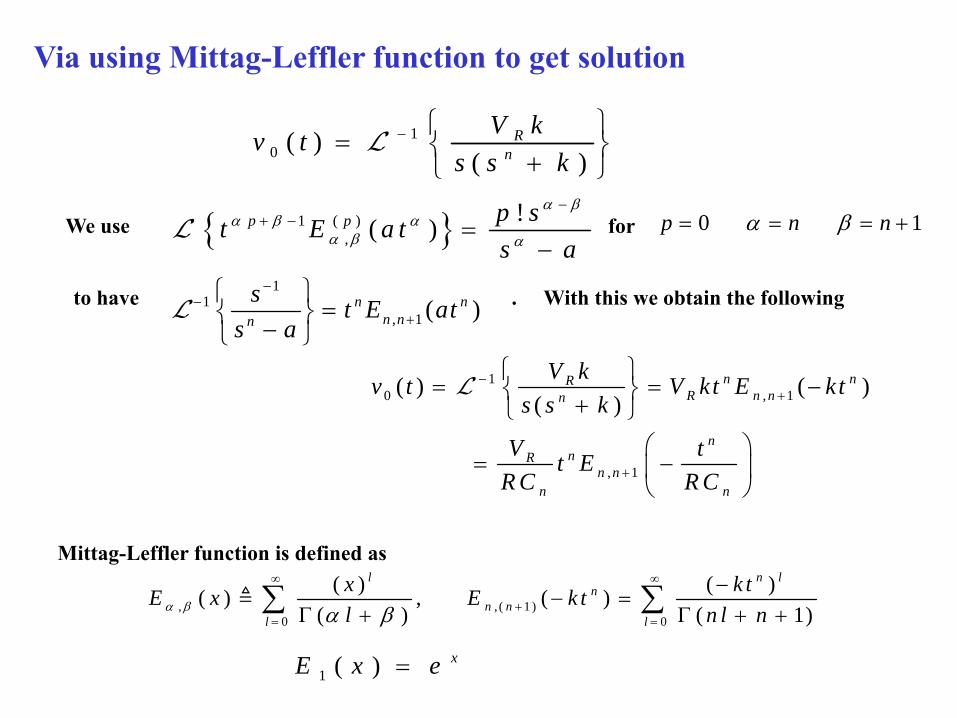
10 ( )
( )R
n
V kv ts s k
− ⎧ ⎫= ⎨ ⎬+⎩ ⎭L
We use for{ }1 ( ),
!( )p p p st E a ts a
α βα β α
α β α
−+ − =
−L 0 1p n nα β= = = +
to have . With this we obtain the following 1
1, 1 ( )n n
n nn
s t E ats a
−−
+
⎧ ⎫=⎨ ⎬−⎩ ⎭
L
10 , 1
, 1
( ) ( )( )
n nRR n nn
nnR
n nn n
V kv t V kt E kts s k
V tt ER C R C
−+
+
⎧ ⎫= = −⎨ ⎬+⎩ ⎭
⎛ ⎞= −⎜ ⎟
⎝ ⎠
L
, , ( 1 )0 0
( ) ( )( ) , ( )( ) ( 1)
l n ln
n nl l
x k tE x E k tl n l nα β α β
∞ ∞
+= =
−− =
Γ + Γ + +∑ ∑Mittag-Leffler function is defined as
1 ( ) xE x e=
Via using Mittag-Leffler function to get solution

Mittag-Leffler function
( )E tα −

0 , 1
0
( ) 1
F o r 1
( ) (1 )
n nnR
R n n nn n n
tR C
R
Vt tv t V E t ER C R C R C
n
v t V e
+
−
⎡ ⎤⎛ ⎞ ⎛ ⎞= − − = −⎢ ⎥⎜ ⎟ ⎜ ⎟
⎢ ⎥⎝ ⎠ ⎝ ⎠⎣ ⎦
=
= −
For charging current of circuit
For charging voltage of capacitor
{ }1 1
( ) u sin g ( )1( ) 1
( )
For 1
( )
R n nnR R
n nn
nnn
nR
nn
tR RC
VV V s ssI s E at
Z s R s ass R R Cs C
V ti t ER RC
nVi t eR
− −
−
⎛ ⎞⎜ ⎟⎜ ⎟= = = =
−⎛ ⎞ ⎜ ⎟++ ⎜ ⎟⎜ ⎟ ⎝ ⎠⎝ ⎠⎛ ⎞
= −⎜ ⎟⎝ ⎠
=
=
L
Charge discharge comparison of classical capacitor and fractional capacitor

RV
tcT0
cT
( )inv t
0( )v t
t
0 , 1 ,1
0 ,1 , 1
( ) ; 0( ) ( ) ( )
(0)( ) (0) ( ) ;( ) ( ) ( )
n nn R sR
n n n cn s n s s n s
n nnc R c c
n c c c n n cs n s n s n s
V RV t tv t t E E t TC R R C R R R R C R R
v R V T Ttv t E v v T E t TR R C R R C R R C R R
+
+
⎛ ⎞ ⎛ ⎞= − + − < <⎜ ⎟ ⎜ ⎟+ + + +⎝ ⎠ ⎝ ⎠
⎛ ⎞ ⎛ ⎞= − = = − >⎜ ⎟ ⎜ ⎟+ + + +⎝ ⎠ ⎝ ⎠
0( )cv T
0
( )c cv T ( ) (0)c c cv T v=
Constant voltage charging and discharging voltage profile at super-capacitor
R
sR
nC
( )inv t
0 ( )v t
0t =

S
XC
+
A−
−V
cons tan t current /cons tan t voltagepower sup ply
CCCV
cons tan t currentdisch arg er
3 0 m i n
2U
2t
1U
RU
1t
3UΔ
V o l t a g e ( V )
T i m e ( s )
3 : d r o pU I RΔ −
IEC-62931 Standard to test super capacitor-2007

I
I f−
tdT
cT0
I R
R
I R KU+
≤(1 )IR f+
cT dT
( )i t
( )v t
t
Excitation current profile for charging and discharging andmeasured voltage across the super-capacitor

1 1
1( ) ( ) ( ) ( ) ( ) ( )
0
(1 )( )
1 (1 )( ) ( ) ( )
(1 ) (1 )
c d
c d
c d c
c d
sT sT
sT sTn
sT sT sT sT
n n
t Ti t Iu t I If u t T Ifu t T u t T
t T
I f I IfI s e es s s
F I I f IfV s Z s I s R e es C s s s s
IR IR f e IR fe IF IF f e IF fes s s s s
− −
− −
− − − −
+ +
>⎧= − + − + − − = ⎨ <⎩
+= − +
+⎛ ⎞ ⎛ ⎞= = + + − +⎜ ⎟ ⎜ ⎟⎝ ⎠ ⎝ ⎠
+ += − + + − + 1 2 2 2
(1 )
( ) ( ) (1 ) ( ) ( )
(1 )( ) ( )( ) ( ) ( )( 1) ( 1) ( 1)
(1 )( ) ( )( ) ( ) ( )
( )(
d c dsT sT
n
c dn nn
c dc d
c dc d
I I f e Ifes C s C s C s
v t IR u t IR f u t T IR fu t T
IF f t T IF f t TIF t u t u t T u t Tn n n
I f t T If t TIt u t u t T u t TC C C
IFv t IR
− −
+
++ − +
= − + − + − +
+ − −+ − − + − +Γ + Γ + Γ +
+ − −+ − − + −
= +Γ
(1 ) (1 )( ) (1 ) ( ) ( ) ( )1) ( 1)
( ) ( ) ( )( 1)
n nc c c
nd d d
I IF f I ft t u t IR f t T t T u t Tn C n C
IF f IfIR f t T t T u t Tn C
⎡ ⎤ ⎡ ⎤+ ++ − + + − + − − +⎢ ⎥ ⎢ ⎥+ Γ +⎣ ⎦ ⎣ ⎦
⎡ ⎤+ + − + − −⎢ ⎥Γ +⎣ ⎦
1( ) n
FZ s Rs C s
= + +
Detailed calculations of voltage profile for constant current charge discharge cycleImpedance of super-capacitor
RF C
( )i t
( )v t

Revised Test Procedure
( ) ( ) ( ) ( ) ( )
(1 ) (1 )( ) ( ) (1 ) ( ) ( ) ( )( 1) ( 1)
( ) ( ) ( )( 1)
c d
n nc c c
nd d d
i t Iu t I If u t T Ifu t T
IF I IF f I fv t IR t t u t IR f t T t T u t Tn C n C
IF f IfIR f t T t T u t Tn C
= − + − + −
⎡ ⎤ ⎡ ⎤+ += + + − + + − + − − +⎢ ⎥ ⎢ ⎥Γ + Γ +⎣ ⎦ ⎣ ⎦
⎡ ⎤+ + − + − −⎢ ⎥Γ +⎣ ⎦
Use the current excitation and voltage profile equations to fit the curve of voltage profileto extract the parameters from following set of expressions, , (or ) ,nR C F C n
Under development

Self discharge with memory via fractional derivative for super-capacitor
A capacitor is charged from time –T to t with a constant voltage Uo; the charging current is
0 0 0
0
d (1 ) (1 )( ) ( ( ))d (1 )
0 1 ( ) 0( )
t tn nn
c n n nn nT T
nn
U d U Un ni t C t Tt h dt h n
U n t Th t T
−
− −
⎛ ⎞Γ − Γ −= = = − −⎜ ⎟Γ −⎝ ⎠
= < < + >+
At t = 0 it is kept in open-circuit; there will be self discharge thus a discharge current willappear depending on decaying terminal voltage u ( t )
0 0
d ( ) (1 ) d ( )( )d d
t tn n
d n n nn
u t n u ti t Ct h t
Γ −= =
We combine the charge and self discharge together and write ( ) ( ) 0c di t i t+ =
0 (1 ) d ( ) 0( ) d
n
n nn n
U n u th t T h t
Γ −+ =
+
Do fractional integration of order n for above expression, to write the following
[ ]00 0
(1 ) ( ) 0( )
nt n
n n
U nD u t Uh t T h
− ⎡ ⎤ Γ −+ − =⎢ ⎥+⎣ ⎦
We apply the formula for fractional integration i.e. to get[ ]0 1-0
1 ( )d( )( ) ( - )
tnt n
f x xD f tn t x
− =Γ ∫
Contd…

Contd…0
010
1 d (1 ) (1 )( ) 0( ) ( ) ( )
t
n nn n n
U x n nu t Uh n T x t x h h−
⎡ ⎤Γ − Γ −+ − =⎢ ⎥Γ + − ⎣ ⎦
∫
Rearranging the above, we write0
0 10
d( )( ) (1 ) ( ) ( )
t
n n
U xu t Un n T x t x −= −
Γ Γ − + −∫
Put T x τ+ = d dx τ= so for 0x = Tτ = and x t= T tτ = + We have thus
0 00 01
d( ) ( )d( ) (1 ) ( ) ( ) (1 )
T t T t
n nT T
U Uu t U U Fn n T t n n
τ τ ττ τ
+ +
−= − = −Γ Γ − + − Γ Γ −∫ ∫
Now we break as and call the second term as ( )dT t
TF τ τ
+
∫0
0
( )d ( )d ( )dT t T t
T T
F F Fτ τ τ τ τ τ+ +
= +∫ ∫ ∫ ( )tI
1 1 10 0 0
d d 1 1( ) ( )d *( ) ( )
T t T t t
n n n n n nt FT t t t t
τ ττ ττ τ τ τ
+ +
− − −⎛ ⎞ ⎛ ⎞= = = = ⎜ ⎟ ⎜ ⎟+ − − ⎝ ⎠ ⎝ ⎠∫ ∫ ∫I
We write in terms of convolution of two functions
Using Laplace pair we write as { } { } { }(1 )( ) ( ) n nt s t t− − −= = ×L I I L L
( )[ ]1 (1 ) 1
(1 ) 1( 1) (1 ) ( )( ) n n
nn n nss ss− + − − +
Γ − − +Γ − + Γ − Γ= × =I
1
( 1)nn
nts +
Γ +↔
Extracting by inverse Laplace of obtained we get( )tI ( )sI
{ }1 1 1( ) ( ) (1 ) ( ) (1 ) ( )t I s n n n ns
− − ⎧ ⎫⎛ ⎞= = Γ − Γ = Γ − Γ⎨ ⎬⎜ ⎟⎝ ⎠⎩ ⎭
I L L
We used Laplace pair 11s
↔ Contd…
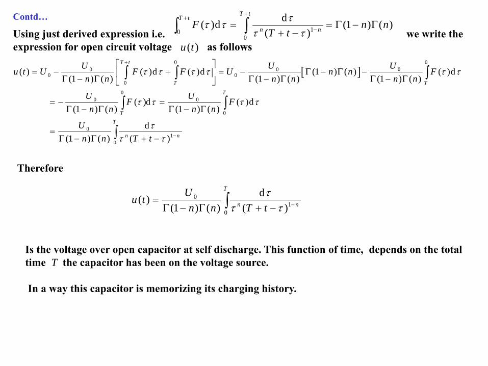
Contd…
Using just derived expression i.e. we write theexpression for open circuit voltage as follows
100
d( )d (1 ) ( )( )
T tT t
n nF n nT t
ττ ττ τ
++
−= = Γ − Γ+ −∫ ∫
( )u t
[ ]0 0
0 0 00 0
0
00 0
0
01
0
( ) ( )d ( )d (1 ) ( ) ( )d(1 ) ( ) (1 ) ( ) (1 ) ( )
( )d ( )d(1 ) ( ) (1 ) ( )
d(1 ) ( ) ( )
T t
T T
T
TT
n n
U U Uu t U F F U n n Fn n n n n n
U UF Fn n n n
Un n T t
τ τ τ τ τ τ
τ τ τ τ
ττ τ
+
−
⎡ ⎤= − + = − Γ − Γ −⎢ ⎥Γ − Γ Γ − Γ Γ − Γ⎣ ⎦
= − =Γ − Γ Γ − Γ
=Γ − Γ + −
∫ ∫ ∫
∫ ∫
∫
Therefore
01
0
d( )(1 ) ( ) ( )
T
n n
Uu tn n T t
ττ τ −=
Γ − Γ + −∫
Is the voltage over open capacitor at self discharge. This function of time, depends on the total time T the capacitor has been on the voltage source.
In a way this capacitor is memorizing its charging history.

Self Discharge Curve of Super-capacitor
10 100 1000
2.5
1.0
2.0
Open CircuitVoltage ( V )
time
log ( t )
At this instant open circuit is done
Self Discharge voltage after open circuit is u ( t ) is almost constant for about time T then it decays as (1 )nt − −
More time the capacitor is kept at charge the more time it takes to self-discharge
T = 10hr
T = 100hr
T = 1000hr
This interesting observation we described by use of fractional derivative

We take example of super-capacitor electrodea rough electrode
Rough electrode
++++++++++++++
-------------Smooth electrode

Collector
Collector
Rough and Porous Electrode

A porous electrode
Metal
CAG electrode
CAG electrode
CAG electrode
electrolyte
Rs : Solution Resistance
CD : Double Layer Capacity
Rs Rs Rs Rs
CD CD CD CD

Transmission line for porous electrode
dR xdC x
i di i+
d- i
de e+e
( d ) d d d d d 0
( d ) d ( d ) d d d 0
e ee e e e iR x e x iR x iRx x
e e i ei i i i C x i x C x Ct x t x t
∂ ∂− + = − = = = − + =
∂ ∂∂ ∂ ∂ ∂ ∂
− + = − = = = − + =∂ ∂ ∂ ∂ ∂
(1)
(2)
Differentiate (1) w.r.t t and differentiate (2) w.r.t x, and combine to get2
2 0i iR Cx t
∂ ∂− =
∂ ∂Differentiate (1) w.r.t x and differentiate (2) w.r.t t, and combine to get
2
2 0e eR Cx t
∂ ∂− =
∂ ∂
Rather we got Fickian diffusion equation for current and voltage

Impedance of the porous electrode system2
2 0e eR Cx t
∂ ∂− =
∂ ∂Let us take , where is actually . Take the time Laplaceand get
e ( , )e x t
2
2
d 0d
e R C s ex
− = with , i.e. Laplace of ( , )e e x s≡ ( , )e x t
Exciting with step input at t = 0 or( 0 , )e t E= ( 0 , ) Ee ss
=
The solution is ( , ) x R C sEe x s es
−=
0e iRx
∂+ =
∂From the equation (1) i.e. , we get current as
1 ( , ) 1( , )
(0, )
x RCs x RCse x s E Ei x s RCs e RC seR x R s Rs
Ei s RC sRs
− −∂ ⎛ ⎞⎡ ⎤= − = − − =⎜ ⎟⎣ ⎦∂ ⎝ ⎠
=
Therefore impedance is (0 , ) RZ sC s
=
From this we may write volt-current expression as
d( ) ( ) 0 .5d
n
n
Ci t e t nR t
= =
This is for infinite field diffusion, the transmission line extends to infinity

More complications
Ionic conduction in the pore electrolyte and electronic conduction in solid phase
Charging of double layer at the solid liquid interface
A simple charge transfer reaction (ct) at the interface
c t dg x dC x
1dR xElectrolyte Ionic Current
Solid Phase Electronic Current
2
ct2
1e eC g et R x
∂ ∂= +
∂ ∂0
ct( )c
s
A S j nFgR T
=
This ct reaction is for Faradic super-capacitors. Our CAG is non-Faradic system
Other improvements include finite field diffusion when we are truncating this infinitetransmission line, consider the finite diffusion of transport species etc.
On the gct we also add hindrance factor
2 dR x

Metal
Electrolyte
Paasch et al and R De Levie analysis
Thickness dArea A
dx
1ϕ
2ϕ
dG1dR
2dR
d ddd 1, 2i
i
G g A xxR i
Aρ
=
= =
( ) ( )1 21 2 1 2
1 2
d dd 1 d 1d d d d
g gx x x x
ϕ ϕϕ ϕ ϕ ϕρ ρ
− = − − − = −
The decay length is 1 2R e ( )gλ ρ ρ⎡ ⎤= +⎣ ⎦
Constituting equations are
The interconnection conductance g we assume charge transfer (ct) , which is hindered in series by finite diffusion, both in parallel with double layer capacity C. The C is double layer capacity perunit area and S is the pore area per unit volume. The contains the standard exchange currentdensity of the ct process. The finite diffusion hindrance is contained by Y.
( )0 00 0j j
s s
j n F j n Fg C S YS C S YR T C R T
ω ω ω ω= + + = + =
0ω0j
g ≡ C S0
s
j nF YSR T

Finite diffusion hindrance and Impedance function( ) 0
0 0j sj R Tg C S YC F
ω ω ω= + =1
22
2 3 23
j1 co thj p
kYl
ω ω ω ωω ω
−⎡ ⎤
= + = =⎢ ⎥⎢ ⎥⎣ ⎦
DD
D is the diffusion coefficient of the electro active species, is rate constant of redox electrodereaction equal to and is characteristic pore dimension. This defines diffusionas finite owing to small pore size.
k
red o xk k+ pl
The complex decay length is now2
11 2
0 1 2
1j ( )d Y CS d
ωλ ωω ω ρ ρ
⎛ ⎞ = =⎜ ⎟ + +⎝ ⎠
2 21 2 1 2 1 2
1 2 1 2 1 2
2 1co ths in h
A dZd d
d
ρ ρ ρ ρ ρ ρλλρ ρ λ ρ ρ ρ ρ
+⎛ ⎞ ⎛ ⎞= + +⎜ ⎟ ⎜ ⎟+ + +⎝ ⎠ ⎝ ⎠
The impedance function of porous electrode is

The Nyquist Plot of Paasch and R De Levie Impedance
0ω1ω
2ω
3ω
R e Z
Im Z−
0 .1dλ
=
1 0dλ
=
1 0 0 2 0 0 3 0 0 4 0 0 5 0 0
1 0 0
2 0 0
3 0 0
4 0 0
5 0 0
Thin electrodeThick electrode
2 21 2 1 2 1 2
1 2 1 2 1 2
2 1co thsin h
A dZd d
d
ρ ρ ρ ρ ρ ρλλρ ρ λ ρ ρ ρ ρ
+⎛ ⎞ ⎛ ⎞= + +⎜ ⎟ ⎜ ⎟+ + +⎝ ⎠ ⎝ ⎠

Non-linear regression analysis of complex Nyquist plot byequivalent circuit with lumped parametersRandles circuit
1R adR WZ adC
C P E
C P E Constant Phase Element C P E1 0 1
( j ) nZ nC ω
= < <
1R High frequency series resistance R e Z ω → ∞
adR Charge transfer (ct) resistance
adC Adsorption capacitance
WZ Generalized Warburg Impedance (diffusion)2
W
co th ( j )( j )
D pR lZ
α
α
τωτ
τω
⎡ ⎤⎣ ⎦= =D
DR Limiting diffusion resistance

The phase angle vis-à-vis frequencyExplanation of this electro-chemical Nyquist plot by R De Levie
At low frequencies the electro-active contents of the pore are used up within a small fraction of acycle, the electrode reaction behaving as capacitance (RC Transmission line), with phase angle as45 degree. At increasing frequencies the rate of diffusion of electro-active species towards and fromthe electrode becomes over-all determining (the corresponding phase angle is 22.5 degree). At stillhigher frequency the finite reaction takes over (the transmission line is R-R system with 0 degreeas phase angle. Finally at the highest frequency the double layer capacitance will dominate (againRC transmission line) with phase angle 45 degree.
045
022 .5
00
ω
Pore Exhaustion
Diffusion
ElectrodeReaction
Double LayerCapacity Im Z−
R e Z
0ω →
1ω 2ω 3ω 4ω 5ω 6ω
ω→∞
1ω2ω3ω
4ω5ω6ω
04 502 2 . 5
04 5
0
Piece wise continuous diagram of Nyquist Plot-showing phase angles withfrequency
In actual cases these zones may extend into each other
02 2 . 504 500 00

In fact solid state Ionics people often do just that !!
To characterize electrical properties –We do impedance spectroscopy measurementsPlot IMAGINARY PART OF IMPEDANCE – Z’’ against REAL PART OF IMPEDANCE Z’On a COLE-COLE PLOT, and use some equivalent circuit, use CPE
We did a new approach based on fractional calculus for anomalous diffusionhttp://arxiv.org/abs/1503.07121Electrical Impedance Response of Gamma Irradiated Gelatin based Solid
Gelatin, with glycerol as plasticizer, formaldehydeas anti-fungal agent and LiClO4 (x weight fraction)Was cast into films of thickness ~ 300-450 μm
Impedance Spectroscopy was done using HIOKILCR meter for x = 0.25 at room temperatureIn frequency range 50 – 2 MHz (Tania Basu et al.Poster presentation NCSSI-9)
The results are analyzed in 2 different ways1.By fitting with an equivalent circuit using CPE2.Using an analytical fractional calculus approachto take anomalous diffusion in but smooth electrode
Courtesy CMPRC Dept of Phys Jadavpur Univ.

Fractal Electrode-a rough surface of interface
Electrode
Electrolyte
At some Angstrom scale (10nm to 0.1mm) the surface appears to be not smooth. The ideal smooth electrode is only mercury electrode-all others solid electrodes have some degree of roughness at the surface. Therefore the electrolyte interfaces at these irregular interface-the roughness of the electrode electrolyte interface manifests as fractional impedance of super-capacitors. This roughness (rugosity) is cause of frequency dispersion in impedance.
We may characterize these rough geometry of the surface via fractal dimension (which isnot integer number as 1, 2, 3), rather it is a real number like 2.39. This analysis does not requirewhat is structure of roughness
Mandelbrot's fractal geometry

Fractal “Koch” curve
Step-0
Step-1
Step-2
Step-3
; ( )l L l∈= ∈ =
14, ( ) 43 3 3l lL l⎛ ⎞ ⎛ ⎞∈= ∈ = =⎜ ⎟ ⎜ ⎟
⎝ ⎠ ⎝ ⎠
24, ( ) 169 9 3l lL l⎛ ⎞ ⎛ ⎞∈= ∈ = =⎜ ⎟ ⎜ ⎟
⎝ ⎠ ⎝ ⎠
34, ( ) 6427 27 3l lL l⎛ ⎞ ⎛ ⎞∈= ∈ = =⎜ ⎟ ⎜ ⎟
⎝ ⎠ ⎝ ⎠
3l
∈=
9l
∈=
27l
∈=4( )3
n
L l⎛ ⎞∈ =⎜ ⎟⎝ ⎠
Mandelbrot's fractal geometry
Repeating it ad infinitum yields a mathematical monster: a continuous curve of infinite length whichis no where differentiable
ln 4 1.2619ln 3fd = = This fractal dimension is measure of rugosity

Scaling of CPE
As mentioned earlier a CPE (constant Phase Element) is a Fractional Power Frequency Dependence(FPFD) where we write admittance as , the exponent is fractional number 0.5 to 1( )1 jY
Zασ ω= = α
The ratio of complex admittance at frequency and is a real number for any scale factork
ω kω
( ) ( )
( )
j / 2( ) j cos jsin ( j) (0 j) cos jsin2 2 2 2
( ) j cos jsin2 2
( )( )
Y e
Y k k k
Y k kY
αα α α α π
α α α
α
απ απ απ απω σ ω σω
απ απω σ ω σ ω
ωω
⎡ ⎤= = + = + = = +⎢ ⎥⎣ ⎦⎡ ⎤= = +⎢ ⎥⎣ ⎦
=
ImY
ReY
•
•
1x
1y
1k xα
1k yα
1ω
1kω
( ) 1 11 1
1
( ) tan2
yY Y kx
απω ω −∠ = ∠ = =
The phase angle of CPE is constant at all frequencies.
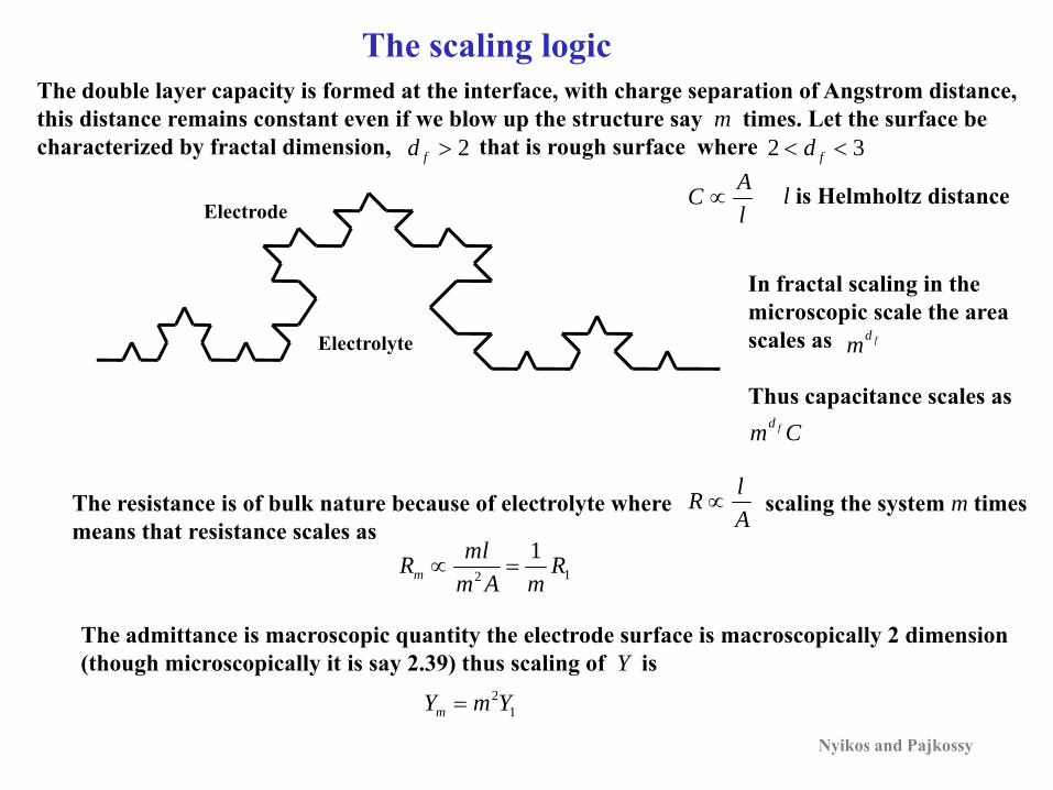
Electrode
Electrolyte
The scaling logic The double layer capacity is formed at the interface, with charge separation of Angstrom distance, this distance remains constant even if we blow up the structure say m times. Let the surface be characterized by fractal dimension, that is rough surface where2fd > 2 3fd< <
ACl
∝
In fractal scaling in themicroscopic scale the areascales as
Thus capacitance scales as
fdm
fdm C
The resistance is of bulk nature because of electrolyte where scaling the system m timesmeans that resistance scales as
lRA
∝
12
1m
mlR Rm A m
∝ =
l is Helmholtz distance
The admittance is macroscopic quantity the electrode surface is macroscopically 2 dimension(though microscopically it is say 2.39) thus scaling of Y is
21mY m Y=
Nyikos and Pajkossy

The derivation of frequency scaled Y via spatial scaling logic 1 j j1
j j 1 jj
1 j
i i ii i i
i i i i
i
i i i
R C CZ R YC C R CCYR C
ω ωω ω ωωω
+= + = =
+
=+∑
We blow up spatially the element m folds and write the following2 1( .1, ) (1, ) ( .1) (1) ( .1) (1)fd
i i i iY m m Y R m R C m m Cm
ω ω= = =
( )( )
1
1
1
1
j ( . 1 )( . 1 , )1 j ( .1 ) ( . 1 )
j (1 )1 j (1 ) (1 )
j (1 )
1 j (1 ) (1 )
(1, )
f
f
f
f
f
i
i i i
di
di i i
di
di i i
d
C mY mR m C m
m Cm R m C
m Cm
m R C
m Y m
ωωω
ωω
ω
ω
ω
−
−
−
−
=+
=+
=+
=
∑
∑
∑
This above expression relates spatial scaling to frequency dependence (scaling)2( .1, ) (1, )Y m m Yω ω=With and above expression we have
1(1, )(1, )
fdY m mY
ωω
−
=Nyikos and Pajkossy

The fractional exponent in terms of rugosity (fractal dimension)1(1, )
(1, )
fdY m mY
ωω
−
=The spatial scaling gave us
The frequency scaling law for CPE or FPFD (with fractional exponent) is (1, )(1, )
Y k kY
αωω
=
Comparing the two as above we can write 1fdk m k mα−= =( 1) 1fdm mα − =
1( 1) 11f
f
dd
α α− = =−
Therefore a fractional admittance (or impedance) has fractional exponentIn other words the fractional exponent is a measure of surface irregularity
( j )Y αω≈ 11fd
α =−
2fd =The perfect smooth surface , the exponent is a pure capacitor (ideal) behavior1α =
3fd →In the limit the exponent result of a porous electrode (it is a 3D case) 0.5α →
The significance of this result explains the connection of surface roughness and frequency dispersionfor the intermediate values of fractional exponent (0.5 to 1), but also offers a simple comparisonbetween surfaces with widely different morphologies. It is remarkable that the microscopic effectivedimension describes the essential features determining frequency dispersion.
Nyikos and Pajkossy

100 nm
Distribution ( ) of aggregate pores of several sizes, on the electrode surface
r α−∼The SEM image of super-capacitor electrode showing roughness & porous nature (Courtesy CMET Govt. of India Thrissur, Kerala)
CAG Electrode porous and rough

r α−∼ α +∈The disorder can be thus ordered via a ‘power law’ distribution as
This is depicted in the histogram of pore size approximated as power law.
The Fuller mix can be expressed in terms of the grain size ‘distribution function’ as follows
2 .5m in
m in m ax3 .5( ) 2 .5 rr r r rr
ϕ = ≤ ≤
( )rϕ represents the probability distribution function
( )dr rϕ is the fraction of grains with diameter in the interval [ ], dr r r+m ax
m in
( )d 1r
rr rϕ =∫
Fuller’s packing of pores
IJAMAS & Am Math Soc.; S. Das, Pramanik

Frequency
m inrm axr
r α−∼
P o r e - S iz e
Frequency
C ap acitymC
( )a
( )b
a) Showing distribution of pores size, b) Corresponding distribution of capacity
Pore size distribution and its capacity
IJAMAS & Am Math Soc.; S. Das, Pramanik

d bxx
Charge distribution at cleavage of electrode crystal
Formation of double layer capacity
Electrode material we consider as simple case made of positive nuclei on fixed ‘regular’ grid points inside a sea of homogeneous distribution of negative charge. By cleaving the electrode one obtains two halves which can be considered as electrodes; the cleaving is at location, as depicted. Let us assume that cleavage has made interface of metal (electrode) and organic (electrolyte), and immediate picture of negative charge sea.
bx
bx x
Q−
IJAMAS & Am Math Soc.; S. Das, Pramanik

bx
bx
bx
x
( )a
( )b
( )c
( )d
Q−Δ
Q−
Q−
Q+
Q Q+ Δ
Q Q− − Δ
Double layer capacity
This spatial charge separation forms “capacity”; the metal-electrolyte capacity-and formation of double layer capacity mC
( )
( )
[ ( )]( )d
( )d
[ ( )]( )d
( )d
b
b
b
b
x
bm x
bxm
x
Q x x x xx
Q x x
Q x x x xx
Q x x
+ −∞
−∞
∞
−∞
Δ −=
Δ
Δ −=
Δ
∫∫
∫∫
( ) ( )1 ( )4m m mC x xπ
+ −= −
( )mx −
( )mx +
Electric fieldPerpendicular to electrode
IJAMAS & Am Math Soc.; S. Das, Pramanik

The distribution function is different for different cleavage. Some cleavage may be symmetrical, as ideal as shown some may have different nuclei distribution near cleavage, with different numbers as per crystal face cleavage of electrode. This distribution thus gives rise to several time-constant system, better described by fractional calculus, with unique disorder parameter .
Now if the above obtained capacity is same, assuming electrode surface is uniformlysmooth, then we do not have problem to model; the capacitor system. However, due torough nature the charge distribution function at each of the cleavage is different-the distribution does not and need not be a normal, Gaussian type. This fractal chargedistribution can lead to a capacity of ‘rough’ electrode other than normal or Gaussiandistribution-leading to power law distribution too! This is ‘disordered’ system.
Disordered system
IJAMAS; & Am Math Soc.; S. Das, Pramanik

( )1
( , ) ( , ) ( ) 0u t u t tt
αλ λ λ δ α∂+ = >
∂
Consider a partial differential equation (PDE)
The above PDE is having free parameter λ
Now if for the free parameter 1α = then we have single time constant system 1λ τ −=
( , ) exp( )u t tλ λ= −with solution as with initial condition ( , 0 ) 1u λ =
The several time constants (discharge rate) is taken as power law distribution as ( )qλ
1 / 0 1q α α= < <
The strong-discharge or exponential discharge with one time constant follow a normal distribution with well defined average that represents average time constant or discharge rate, and that normal distribution has well defined standard deviation. Unlike the normal distribution the ‘power-law’ distribution has no defined average or moments (standard deviation); and is representation of system which has variety. The heterogeneity or the disordered system thus has varieties of ways by which dissipation mechanism takes place.
A several time-constant system-no average
IJAMAS; & Am Math Soc.; S. Das, Pramanik

( )1
( , ) ( , ) ( )u t u t tt
αλ λ λ δ∂+ =
∂
( )1( , ) ( , ) e x pu t h t tαλ λ λ= = −
( , )h tλ denotes ‘impulse response function’. On integrating this ‘impulse response function’ for free variable we get the function of time and that is called ‘impulse response’ Green’s function
( )1
0 0
(1 )( ) ( , ) ex p dg t h t d tt
αα
αλ λ λ λ∞ ∞ Γ +
= = − =∫ ∫1 (1/ )( / ) d ( / )dx t t xα αλ λ λ α−= =
1( 1 / )
0 0
11
10 0
( ) d d
( )d d
(1 )
x x
x x
x xg t e x e xt t t t
xe x e x xt t t t
t
αα
αα
α α α
α
α αλ λ
α α α α
α
−∞ ∞− − −
∞ ∞−− − −
−
⎛ ⎞ ⎛ ⎞ ⎛ ⎞ ⎛ ⎞= =⎜ ⎟ ⎜ ⎟ ⎜ ⎟ ⎜ ⎟⎝ ⎠ ⎝ ⎠ ⎝ ⎠ ⎝ ⎠
Γ⎛ ⎞ ⎛ ⎞= = =⎜ ⎟ ⎜ ⎟⎝ ⎠ ⎝ ⎠Γ +
=
∫ ∫
∫ ∫
Steps are
Using the Gamma definition
1
0
( ) d
( ) (1 )
ye y yαα
α α α
∞− −Γ
Γ = Γ +
∫
“Impulse response function” to “Impulse response”
To get above substitute
IJAMAS; & Am Math Soc.; S. Das, Pramanik

( )1
( , ) ( , ) ( )u t u t f tt
αλ λ λ∂ ′+ =∂
Then the response to this new excitation is convolution of Green’s function obtained above with the forcing function that is:
0 0
( )( ) ( ) * ( ) ( ) ( )d (1 ) d 0 1t t f tr t g t f t g f t α
ττ τ τ α τ ατ′ −′ ′= = − = Γ + < <∫ ∫
Multiplying and dividing the above expression with (1 )αΓ −
[ ]
( )
0(1 )
( )( ) (1 ) (1 ) ( )d(1 )
(1 ) (1 ) ( )
(1 ) (1 ) ( )
t
t
t
tr t f
D f t
D f t
α
α
α
τα α τ τα
α α
α α
−
− −
− ′= Γ + Γ −Γ −
′Γ + Γ −
= Γ + Γ −
∫
Implying the appearance of fractional derivative for cases where several time-constants define arelaxation process. Therefore a disordered relaxation (response) may well be formulated by fractionaldifferential equation, the order giving the ‘intermittency’ of relaxation disordered process!
Using definition of fractional integral
Fractional derivative operator-in disordered system
10 0
0
1( ) ( ) ( ) ( )( )
t
t tI f t D f t t f dγ γ γτ τ τ γγ
− − += = − ∈Γ ∫
We get
IJAMAS & Am Math Soc.; S. Das, Pramanik
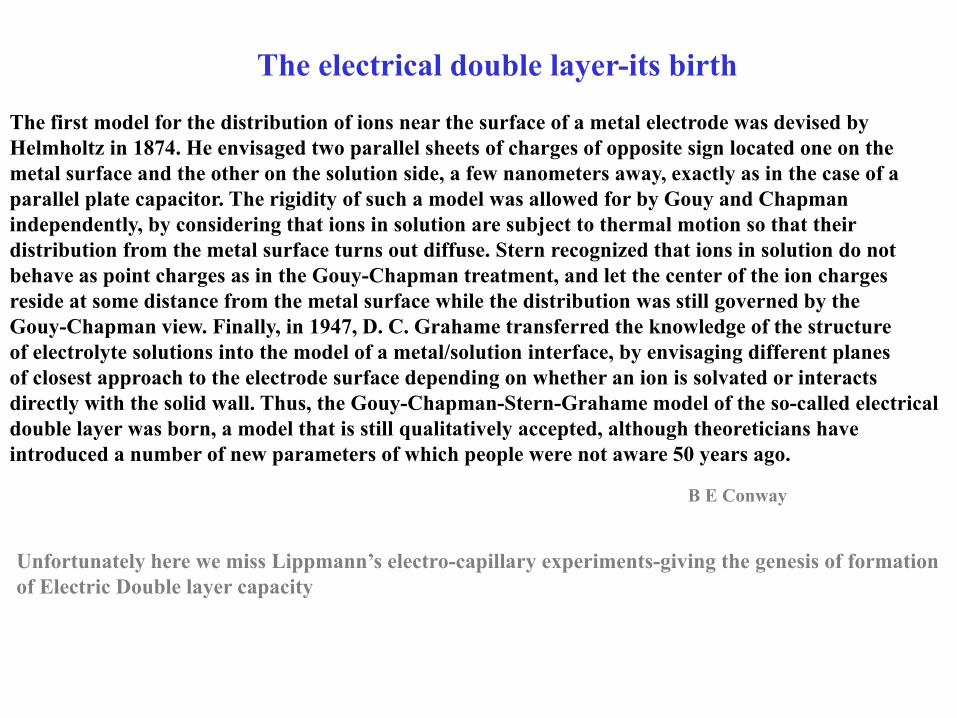
The electrical double layer-its birth
The first model for the distribution of ions near the surface of a metal electrode was devised by Helmholtz in 1874. He envisaged two parallel sheets of charges of opposite sign located one on the metal surface and the other on the solution side, a few nanometers away, exactly as in the case of a parallel plate capacitor. The rigidity of such a model was allowed for by Gouy and Chapman independently, by considering that ions in solution are subject to thermal motion so that their distribution from the metal surface turns out diffuse. Stern recognized that ions in solution do not behave as point charges as in the Gouy-Chapman treatment, and let the center of the ion charges reside at some distance from the metal surface while the distribution was still governed by the Gouy-Chapman view. Finally, in 1947, D. C. Grahame transferred the knowledge of the structure of electrolyte solutions into the model of a metal/solution interface, by envisaging different planes of closest approach to the electrode surface depending on whether an ion is solvated or interacts directly with the solid wall. Thus, the Gouy-Chapman-Stern-Grahame model of the so-called electrical double layer was born, a model that is still qualitatively accepted, although theoreticians have introduced a number of new parameters of which people were not aware 50 years ago.
B E Conway
Unfortunately here we miss Lippmann’s electro-capillary experiments-giving the genesis of formationof Electric Double layer capacity

The electro-chemical double layer
Dates back to 1875 where Lippmann experimented with variable potential to Mercury and electrolyteHg2 Cl2 and measured surface tension of mercury via capillary phenomena. The curves he obtainedwere called Electro-Capillary curves. The Lippmann equation governing charge (rather excess charge)to change in surface tension is also called Electro capillary equations
dd
qEγ
= −
If C is defined as differential capacitance per unit area then
,
2def
2,el el TT
qCE Eμ μ
γ⎛ ⎞∂ ∂⎛ ⎞= = − ⎜ ⎟⎜ ⎟∂ ∂⎝ ⎠ ⎝ ⎠Therefore the double layer capacity is due to double rate of change of surface tension
If C is constant the Lippmann curve is parabola a convex one
Lippmann curves Lippmann experiment scheme
D C Grahme

Some remarks about Electro-capillary curvePZC Point of zero charge
Negative polarizationPositive polarization
The physical mechanism of electro-capillary effect is attributed to accumulation of surface chargeof equal magnitude of opposite sign on each side of an interfacial boundary. Any such narrow region (10-200 Angstrom) supporting such separation is termed as Electric Double Layer Capacity.
The voltage at which surface tension is maximum peak of electro-capillary curve is PZC and represents the point at which the net charge on each side of interface boundary is zero.
The mutual repulsion of the charges tangential to the interface leads to an effective decrease in thesurface tension
Up to 2-3 Volts the interface draws a very little current-behaves like ideal polarizable electrode.

Possible charge distribution at the interfacePZC Point of zero charge
Negative polarizationPositive polarization
Metal
+
+++++++
+
+
+
+
+
+
+
+
Electrolyte
Negative polarization
q−q
Metal Electrolyte− +− +− +− +− +− +− +− +− +− +− +− +− +− +− +− +
−−−−−−−−−−−−−−−−
0q=
PZC Positive polarization
++++++++
Metal
−
−
−
−
−
−
−
−
Electrolyte
Positive polarization: Excesspositive charge on metal side,and some negative charge areadsorbed giving a ‘compactdouble layer’PZC: Negative charges adsorbedat interface
Negative polarization: Excess negative charge on metal side, noadsorbed charges, giving a diffusedouble layer
D C Grahme
Though not very convincing!

ConclusionWe get frequency dispersion for impedance of super-capacitor when we carry outImpedance spectroscopy.
We get non ideal curves for circuits with super-capacitor charging discharging
The double layer formation is via changes in surface tension and thermodynamics
The internal of super-capacitors are heterogeneous: are porous, are rough are havingseveral time constants of relaxation
Classical electro-chemical laws give the distributed parameter R C cases
The fractal electrode also relate to non-ideality of super-capacitor vis-à-vis ideal one.
The FRACTIONAL DERIVATIVE embeds many of these observations, to representthis non-ideal capacitor, without knowing internal structure, electro-chemical detailsthe internal distributed R C structure or the fractal dimension of the electrode-butonly from two terminals of the devise of. super-capacitor
Perhaps a new way to represent the circuit element super-capacitor-and use fractionalorder circuit theory

ReferencesThe Electrical double layer & theory of electro-capillarity; D C Grahme.Electro-chemical super-capacitors: Scientific Fundamentals & Technological Applications; B E Conway.Theory of electrochemical impedance of macro homogeneous porous electrode; G Paasch et al.Fractals and rough electrodes; R De Levie.On porous electrodes in electrolyte solutions; R De Levie.Fractal dimension and fractional power frequency dependent blocking electrodes; Nyikos and Pajkossy.Diffusion to fractal surface; Nyikos and Pajkossy. Diffusion to fractal surfaces-II verification of theory; Nyikos and Pajkossy.Fractal Geometry of Nature; Mandelbrot.Self discharge and potential recovery phenomena at thermally & electrochemical prepared RUO2 super-capacitorElectrodes; Liu, Pell, Conway.Electromechanics of fluid double layer system; Joseph Charles Zuercher.Electric Double layer characteristics of nano-porous carbon derived from Titanium Carbide; Permann et al.Advanced nano-structured carbon material for electric double layer capacitor; A Janes, et al.Impedance modeling of porous electrode; H Gohr.Impedance of inhomogeneous porous electrode (a novel transfer matrix calculations); Paasch & Nguen.Indigenous development of Carbon Aerogel Super Capacitors and application in Electronic Circuit; S Das & PramanikBARC News Letter. Micro-structural Roughness of Electrodes Manifesting as Temporal Fractional Order Differential Equation in Super-Capacitor Transfer Characteristics; IJAMAS & Am. Math. Soc. S Das, N C Pramanik. DEVELOPMENT OF SUPERCAPACITOR & APPLICATIONS IN ELECTRONICS CIRCUITS PROJECT REPORT-BRNS; N C Pramanik.Electrical Impedance Response of Gamma Irradiated Gelatin based Solid, Tania Basu, Abhra Giri, Sujata Tarafdar, Shantanu Das Applying Fractional Calculus in Solid State Ionics, Sujata TarafdarFunctional Fractional calculus 2nd Edition (Spriger-Verlag Germany); S. Das.

Thank-you