cadence ddr3 design in intro - in2p3 the ddr3 design challenges using cadence ddr3 design-in kit...
TRANSCRIPT

Addressing the DDR3 design challenges using Cadence DDR3 Design-In Kit
Martin Biehl ([email protected])Ecole d'électronique numériqueFréjus27.Nov.2012

Agenda
1. Key Design Challenges
2. DDR3 Design-In IP
3. DDR3 Design-In Flow & Methodology
2 © 2012 Cadence Design Systems, Inc. All rights reserved.
3. DDR3 Design-In Flow & Methodology

Timing Budget Signal Quality
DDR3 Board and IC Package
design
Key Design Challenges for DDR3
3 © 2012 Cadence Design Systems, Inc. All rights reserved.
Component parameters and
selectionStack-up and Layout
Large solution spaceTo be explored

Key Design Challenges- Timing Budget
� Set-up / Hold Times− Data write w.r.t strobe− Data read w.r.t strobe− Addressing w.r.t clock
4 © 2012 Cadence Design Systems, Inc. All rights reserved.
� Strobe w.r.t clock− Data w.r.t Address
� Account for − Clock/Strobe Jitters and Interconnect Jitters− Slew-rates and hence derating of setup/hold

Key Design Challenges- Signal Quality
� Thresholds − DC and AC− Noise-Margins
� Overshoots/Undershoots − Magnitude− Area
5 © 2012 Cadence Design Systems, Inc. All rights reserved.
− Area
� tVac− Minimum time for signal to stay above threshold
� Eye− Data-Valid Window after accounting Jitter
� Slews that in-turn affect timing− Rise/Fall times

Key Design Challenges- Component Selection
� Memory-Buffers− Trade-off between read-write cycles
� Controller Driver strength− Trade-off between read-write cycles
6 © 2012 Cadence Design Systems, Inc. All rights reserved.
� Connector− Insertion loss
� Strobe/Clock differential buffers− Should satisfy tDVac and overshoot/undershoot area
requirements

Key Design Challenges- Layout Constraints
� Trace-lengths− Relational Propagation-delays Data-Strobe for balanced setup/hold− Relational Propagation-delays Address-Clock for balance setup/hold− Relational Propagation-delays Strobe-Clock for successful write-leveling
� Topology schedules− Point to Point for Data
7 © 2012 Cadence Design Systems, Inc. All rights reserved.
− Point to Point for Data− FlyBy for Address
� Trace Impedance − Example: Lead-in section (45 ohm) to Load-in section (60 ohm) through
neck-down (~5 to 10 mm) for clock− Percentage variation that can be tolerated
� Differential matching (CLK, STROBE)− Maximum unparallel length

DDR3 Design-In Kit Content:Design-In IP!
Connector Model
Controller IO+ IC Package
Model
MemoryModel
Timing/DerationModel
8 © 2012 Cadence Design Systems, Inc. All rights reserved.
Electrical Constraints
DIMM topology
Electrical Constraints
Scripts,Utilities
&Documents

DDR3 Design-In IP
� Frequency: 800/1066/1333/1600� DIMM-Type: A to F � Configuration: 1-slot/2-slot/on-board� Addressing: IT/2T� AC-Threshold levels:150/175
9 © 2012 Cadence Design Systems, Inc. All rights reserved.
� AC-Threshold levels:150/175� Slew-rate based derating

DDR-3 Design-In Flow & Methodology
BuildingProject
Timing Verification
Timing Estimation
ECsetgeneration
IO-model selection
SI solution space
Bus-Analysis
Allegro PCB SI 16.5EMA TimingDesigner 9.2.5

Building Project
� Frequency of operation and AC threshold levels− Configures TD models− Configures custom measurements
� Address (1T / 2T)
11 © 2012 Cadence Design Systems, Inc. All rights reserved.
� Address (1T / 2T)− Configures TD models
� New DIMMs (Or On-board) vs Existing DIMMs− Pre-created Topologies vs Extracted DIMM topologies
� DIMM Card Type− Configures topologies and ECSets

Timing estimation
� Estimate Etch-delays of data-strobe-clock-address such that − all timing
Constraint Description
TDQSS Strobe rising time relative to rising clock edge.
TDSH Strobe falling edge setup time to rising clock edge.
TDSS Strobe falling edge hold time to rising clock edge.
TDS Data setup time
TDH Data hold time
TDIPW Data pulse width
TDQSH Strobe output high pulse width time.
TDQSL Strobe output low pulse width time.
12 © 2012 Cadence Design Systems, Inc. All rights reserved.
− all timing constraints are met
− Balance setup/hold is achieved
− interconnect jitter is tolerated
TCH Clock high pulse width time.
TCL Clock low pulse width time

IO-model selection/Exploration- Card A with Card B
13 © 2012 Cadence Design Systems, Inc. All rights reserved.

Relational topologies- Refine etch-delays for strobe centering
14 © 2012 Cadence Design Systems, Inc. All rights reserved.

Timing Verification after SI-annotation
� Re-verify timing after import of SI propagation-delays
15 © 2012 Cadence Design Systems, Inc. All rights reserved.

� Propagation Delays
� Impedance
Setting up ECSets
16 © 2012 Cadence Design Systems, Inc. All rights reserved.
� RPD
� Max Parallel

Bus Analysis
� Use Signal Jitter & Offset from TimingDesigner diagrams� Use DDR3 derate-file for setup/hold margins
17 © 2012 Cadence Design Systems, Inc. All rights reserved.

DDR3 Design-In IPThe Cadence way to explore and implement the protocol
Etch-delay estimation for
timing
Signal-Integrity checks using
estimated etch-delays
Pre-layout Signal-Integrity to Timing-
closure
18 © 2012 Cadence Design Systems, Inc. All rights reserved.18
delays
Etch-length and Buffer strength (ODT) refinement
for better eye
Generation of layout constraints for board routing based on SI
topologies
Post-layout Bus simulations and
verification
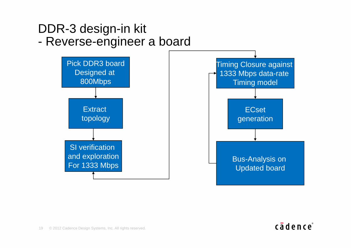
DDR-3 design-in kit - Reverse-engineer a board
Pick DDR3 boardDesigned at
800Mbps
Timing Closure against 1333 Mbps data-rate
Timing model
Extract topology
ECsetgeneration
19 © 2012 Cadence Design Systems, Inc. All rights reserved.
SI verification and explorationFor 1333 Mbps
Bus-Analysis on Updated board

DDR-3 design-in kit - Decide IO-buffer timing parameters
DDR3 reference board
Timing Explorationfor Buffer -TCO delays-Write-leveling delays-PLL jitter / DCDSI extraction of nets
-Propagation delays
20 © 2012 Cadence Design Systems, Inc. All rights reserved.
-Propagation delays-Estimated Xtalk-Stack-up variation
SI verification using SPICE IO-buffer
models

DDR3-design in kit
Full version (IP560): Can be customized and applied to designs
➾ DDR3 custom-measurements and Eye-masks➾ Generic IBIS IO buffers for DDR3 controller and Memory➾ Basic Timing-models for different speed-bins: 800, 1333, 1600Mhz➾ Simulation patterns and setup/hold derate-file➾ Post-route flow with Reference Mother-board and DIMM➾ Pre-route flow using pre-created topologies corresponding to different DIMM cards
21 © 2012 Cadence Design Systems, Inc. All rights reserved.
➾ Pre-route flow using pre-created topologies corresponding to different DIMM cards➾ ECSet templates for guiding routing of boards➾ Enhanced Timing-models
➾ Write-leveling➾ Support for separate package, board, dimm delays➾ Auto-configuration based on DIMM types➾ Hierarchical IC / PCB timing-libraries
➾ Over-clock speed-bins: 1866, 2133Mhz➾ TSMC 28n 2400Mhz IBIS buffers corresponding to Cadence DDR3/4 PHY➾ Reference Package
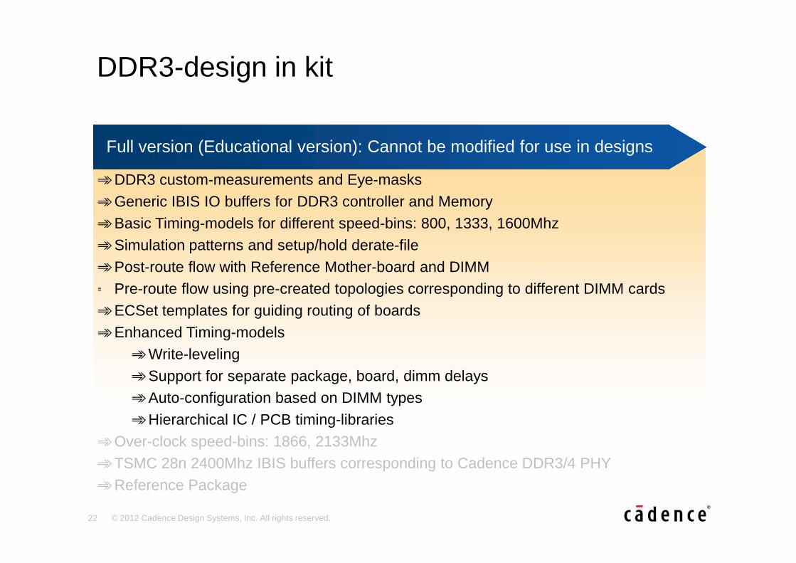
DDR3-design in kit
Full version (Educational version): Cannot be modified for use in designs
➾ DDR3 custom-measurements and Eye-masks➾ Generic IBIS IO buffers for DDR3 controller and Memory➾ Basic Timing-models for different speed-bins: 800, 1333, 1600Mhz➾ Simulation patterns and setup/hold derate-file➾ Post-route flow with Reference Mother-board and DIMM➾ Pre-route flow using pre-created topologies corresponding to different DIMM cards
22 © 2012 Cadence Design Systems, Inc. All rights reserved.
➾ Pre-route flow using pre-created topologies corresponding to different DIMM cards➾ ECSet templates for guiding routing of boards➾ Enhanced Timing-models
➾ Write-leveling➾ Support for separate package, board, dimm delays➾ Auto-configuration based on DIMM types➾ Hierarchical IC / PCB timing-libraries
➾ Over-clock speed-bins: 1866, 2133Mhz➾ TSMC 28n 2400Mhz IBIS buffers corresponding to Cadence DDR3/4 PHY➾ Reference Package

DDR3-design in kit
Lite version (Web download): Abridged version available as demo-vehicle
➾ DDR3 custom-measurements and Eye-masks➾ Generic IBIS IO buffers for DDR3 controller and Memory➾ Basic Timing-models for different speed-bins: 800, 1333, 1600Mhz➾ Simulation patterns and setup/hold derate-file➾ Post-route flow with Reference Mother-board and DIMM➾ Pre-route flow using pre-created topologies corresponding to different DIMM cards
23 © 2012 Cadence Design Systems, Inc. All rights reserved.
➾ Pre-route flow using pre-created topologies corresponding to different DIMM cards➾ ECSet templates for guiding routing of boards➾ Enhanced Timing-models
➾ Write-leveling➾ Support for separate package, board, dimm delays➾ Auto-configuration based on DIMM types➾ Hierarchical IC / PCB timing-libraries
➾ Over-clock speed-bins: 1866, 2133Mhz➾ TSMC 28n 2400Mhz IBIS buffers corresponding to Cadence DDR3/4 PHY➾ Reference Package http://www.cadence.com/products/pcb/Pages/ResourceLibrary.aspx

24 © 2012 Cadence Design Systems, Inc. All rights reserved.