base band application (mt6218b)
TRANSCRIPT
B
Base band application (MT6218B based platform)
WCP/MS/SA1WCP/MS/SA1Danny WangDanny Wang2004/07/072004/07/07

B
Outline
• MT6305 overview• MT6218B overview• Application circuit discussion• Connect to Driver• Base band test items overview• Base band related tools overview• Communication models with customer• END

B
PMIC BaseBand
Ext. ChargerPower
0.2 OHM
FET
VbatBat-TempBat-TypeBattery
Pack
ResetChr_DetChr-cntl
Pwr_BBSR_Clk_En
Pwr_keyChr-drv
Vchr
ResetGPIOGPIO
BuzzerGPIO
Vibrator
BB_WakeupSR_Clk_En
Keypad
Aux_ADC_1
Aux_ADC_2Aux_ADC_3Aux_ADC_4
Vd Vsus Va VioVrtc Vctxo Vm Vsim
Charger
Bat_DetI-charger SIM…
GPIO
M
Buzzer
SIM
LED
V+
MT6305 overview - Block diagram
Rsense

B
Charger state diagram
No chargestate
Charger detected & BATDECT “L” &
Vbat > 3.2V & CHRCTRL “H”
Prechargestate
CC modestate
CV modestate
1. Charger unplugged
2. BATDECT floating
3. OV
4. CHRCTRL “L”Any state
Charger detected & BATDECT “L” &
Vbat > 4.2V & CHRCTRL “H”
Charger detected & BATDECT “L” &
Vbat < 3.2V
Charger detected & BATDECT “L” &
Vbat > 3.2V & CHRCTRL “H”
Charger detected & BATDECT “L” &
Vbat > 4.2V & CHRCTRL “H”
H.W.

B
MT6305 overview - Function (1)
• Regulator– Va, Vtcxo (2.8V, Low noise and high PSRR design, can be turned off in sleep
mode by “VASEL” and “SRCLKEN”, ) – Vm (1.8/2.8V “Vmsel”), – Vcore (1.8V) – Vio (2.8V)– Vsim (3V/1.8V “SIMSEL”)– Vrtc (1.5V) (1mA)
• Reset control– Reset delay (2msec/nF * Crstcap)
• LDOs On/Off control– Charger in > Vbat + 0.25V– BBwake up “H”– OT/UVLO (3.0,3.2)– DDLO (2.5,2.6)

B
MT6305 overview - Function (2)
• Charger function– BATUSE (L Li-ion, H Ni-Mh)– BATDET (L charger enabled) (5usec)
PMIC auto disable charging function if illegal battery is found or battery removal– Precharge function (Li-ion/Ni-MH)
Precharge current = 10mV/Rsense– CC mode charging (Li-ion/Ni-MH)
CC mode charging current = 160mV/Rsense– CV mode charging (only for Li-ion)
Vbat is kept to 4.2V– OV function (5usec)
4.3 V (Li-ion), 5.1V (Ni-MH)• Thermal shutdown (disable all regulator, exclude RTC)• Buzzer, LED, Alerter driver (low Von voltage) • 1.8V/3V SIM level shifter
B
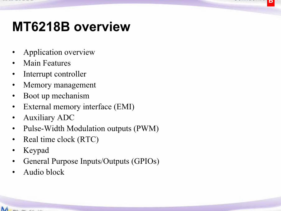
MT6218B overview
• Application overview • Main Features• Interrupt controller• Memory management• Boot up mechanism• External memory interface (EMI)• Auxiliary ADC• Pulse-Width Modulation outputs (PWM)• Real time clock (RTC)• Keypad • General Purpose Inputs/Outputs (GPIOs)• Audio block

B
MT6218B Overview – Typical Application

B
MT6218B Overview – Block Diagram

B
MT6218B Overview – Main Features(1/3)• MCU system and external memory interface
ARM7EJ-S 32-bit RISC processor (26/52MHz)Java hardware acceleration for Java-based games and other applets2M bits zero-wait-state on-chip SRAMOn-chip boot ROM for Factory Flash downloadWatchdog timer for system crash recovery
• External memory interfaceSupport 8/16-bit memory components with size up to 64MB eachSupport Flash and SRAM with page (8/16/32/64 bytes) mode or burst modeSupport Pseudo SRAMStandard parallel LCD interface, built-in hardware acceleration function for color LCD panelsFlexible I/O voltage of 1.8V ~ 3V for memory interface
• Multimedia subsystemDedicated 8-bit parallel interface, support up to 3 external devices(LCM, NAND, Camera)High speed hardware JPEG decoder, image resizerSupport LCD panel maximum resolution up to 800X600 at 16bppInterface for NAND Flash, USB 1.1 device, and MMC/SD/MS/MS pro

B
• Audio and Modem codecWavetable synthesis with up to 64 tonesTwo programmable acoustic compensation filters (Uplink, downlink)AMR/EFR/FR/HR speech codingDial tone generation, voice memo, noise reduction, and echo suppressionSupport GPRS class 12
• User interfaces6-row x 7-column keypad scanSupport three UARTs with speed up to 921600 bpsIrDA modulator/demodulator, Real time clock operationSerial LCD interface with 7 bytes TX FIFOPWM for backlight and alerterSix external level sensitive interrupts with de-bounce logic (FIQ, IRQ don’t)
• Audio interfaceTwo microphone inputs sharing one programmable low noise amplifierTwo speech outputs with dedicate programmable power amplifierHalf-duplex hands-free operation
MT6218B Overview – Main Features(2/3)

B
• Radio interface and baseband front end10 bit DAC for uplink I/Q signals, and 14 bit ADC for downlink I/Q signals10 bit DAC for APC13 bit DAC for for AFCTwo 3-wire control serial interface channels (BSI)10-bit parallel interface with programmable driving strength (BPI)Multi-band support
• Power managementPower down mode for analog and digital circuits independently32KHz slow clocking at standby state7 channel 10-bit ADC for charger and battery monitoring
• Test and debugDigital and analog loop back modes for both audio and base band front-endDAI port complying with GSM Rec.11.10JTAG port for debugging embedded MCU
MT6218B Overview – Main Features(3/3)

B
MT6218B Overview – Interrupt controller
Interruptinput
Multiplex&
Priority mapping
TDMA_CTIRQ2
UART1
RTC
TDMA
SIMDSP2CPU
KEYPAD
GPTimer
EINT
DMA
GPI_FIQ
UART2
GPI
TDMA_CTIRQ1FIQ
controller
IRQcontroller
IRQ0IRQ1IRQ2
..IRQ31
FIQ
IRQ
De-bouncelogic
EINT0EINT1EINT2
NIRQ0000_0018h
0000_001Ch
0000_0000hSystem reset
Level/Edge sensitive
MT6218B
NFIQ
DMA
USB
..
..
..
High priority
EINT3EINT4EINT5EINT6EINT7
32K based
PU

B
MT6218B Overview - Memory management
CS0/1 (16Mbytes)CS2/3 (16Mbytes)CS4/5 (16Mbytes)CS6/7 (16Mbytes)
256MB
B
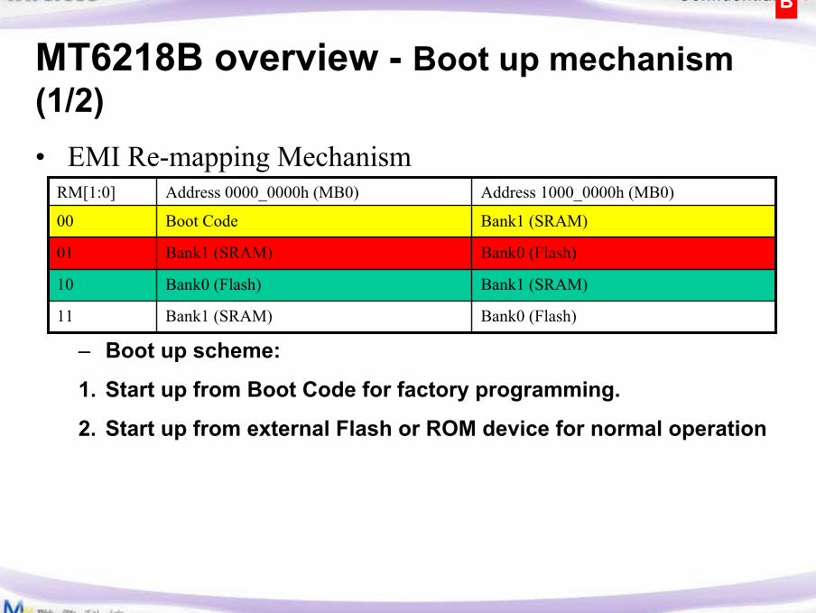
MT6218B overview - Boot up mechanism (1/2)• EMI Re-mapping Mechanism
– Boot up scheme:
1. Start up from Boot Code for factory programming.
2. Start up from external Flash or ROM device for normal operation
Bank0 (Flash)Bank1 (SRAM)11
Bank1 (SRAM)Bank0 (Flash)10
Bank0 (Flash)Bank1 (SRAM)01
Bank1 (SRAM)Boot Code00
Address 1000_0000h (MB0)Address 0000_0000h (MB0)RM[1:0]

B
RTC alarm
USB Mass storage
Received Boot command within150ms
Meta mode
Normal mode
Switch off charging
IBOOT = 0
Download agentYes
No
Normal power on
Test mode power on
MT6218B overview - Boot up mechanism (2/2)• SW State
Exception handler
Any abnormal
B
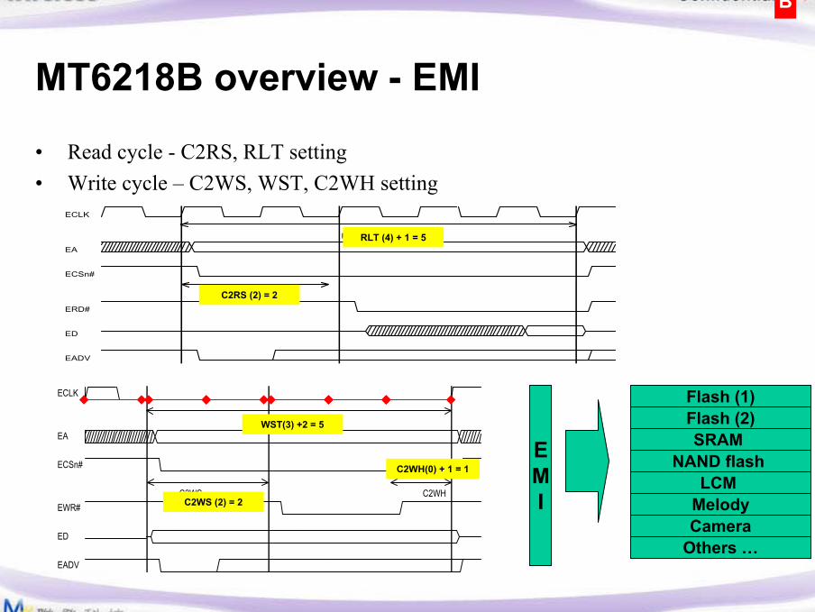
MT6218B overview - EMI
• Read cycle - C2RS, RLT setting• Write cycle – C2WS, WST, C2WH setting
EMI
Flash (1)Flash (2)SRAM
NAND flash LCM
MelodyCamera
Others …
ECLK
RLT+1
EA
ECSn#
C2RS
ERD#
ED
EADV
C2RS (2) = 2
RLT (4) + 1 = 5
ECLK
WST+2EA
ECSn#
C2WS C2WHEWR#
ED
EADV
C2WS (2) = 2
WST(3) +2 = 5
C2WH(0) + 1 = 1

B
MT6218B overview - Auxiliary ADC
• Auxiliary ADC– 7 input channel
10-bit resolution– 2 operation mode
immediate mode timer-triggered mode (*)
– TDMA_AUXEV0 : channel 0 only » Vbat is measured during PA turned on period
– TDMA_AUXEV1 : channel 0,1,2,3,4,5,6 (VBAT, ISENSE)» All ADC channels can be selected to measure during PA
turned off period– Auto or single mode– 8 output data register
DAT0,1,2,3,4,5,6 for CH0,1,2,3,4,5,6 DATA7 for CH0, TDMA_AUXEV0

B
MT6218B overview - PWM
• PWM– PWM1/PWM2– CLK can be 32K or 13M– Internal CLK = CLK or CLK/2 or CLK/4 or CLK/8– Freq. = Internal CLK/(PWM_COUNT + 1)– Duty = PWM_THRES/(PWM_COUNT + 1)
• Alerter – CLK source is 13MHz only
Internal CLK
Threshold
PWM out
PWM_THRES < PWM_COUNT

B
MT6218B overview - RTC
• RTC– Interrupt
Tick condition met– A=(SEC,MIN,HOU,DAY,WEEK,MONTH,YEAR), A/2, A/4,
A/8Alarm condition met
– A – First power on
RTC_PWRKEY1 A357h, RTC_PWRKEY2 67D2h0~2048ms programmable power on debounce time
– Baseband power upBBPU : BBWKEUP
– Write_EN (power off protection)0 : rtc write interface will be disabled until next power on.

B
MT6218B overview - KEYPAD
• Keypad– 7 columns (Input) x 6 rows (Output)– Detect one or two key-pressed simultaneously
COL6 COL5 COL4 COL3 COL2 COL1 COL0
ROW5
ROW4
ROW3
ROW2
ROW1
ROW0
1
1
1
1
1
0
1
1
1
1
1
1
1
1
1
1
1
1
1
1
1
1
1
1
1
1
1
1
1
1
1
0
0
0
0
0
10 0 0 0 0

B
MT6218B overview - GPIOs
• GPIOs– Mode control (2bits)
GPIO,F1,F2,F3Default : GPI
– Direction– Pull-up/Pull down– Output Data
0 1 2 3 Net Name DescriptionGPIO0 DAICLK LPT_CK TDMA_CK DAICLK ReservedGPIO1 DAIPCMOUT LPT_D2 TDMA_D1 GPIO1_LM4890OFF/DAITX Audio amplifiter enable/disableGPIO2 DAIPCMIN LPT_D1 TDMA_D0 DAIRX ReservedGPIO3 DAIRST LPT_D0 TDMA_FS DAIRST ReservedGPIO4 BPI_BUS4 TXEN RFGPIO5 BPI_BUS5 BPI5 RFGPIO6 BPI_BUS6 BFE_PRB0 BANDSW RFGPIO7 BPI_BUS7 BSI_CS1 BPI7 RFGPIO8 LCD_DATA LCDBL_EN Enable(H)/Disable LCD backlight power supplyGPIO9 LCD_A0 GPIO9_RLED Enable(H)/Disable Yellow LEDGPIO10 LCD_CLK GPIO10_GLED Enable(H)/Disable Green LEDGPIO11 /LCD_CS0 GPIO11_BLED Enable(H)/Disable Blue LEDGPIO12 /LCD_CS1 GPIO12_CHRCTRL Enable(H)/Disable PMIC charger block GPIO13 13MHZ MELODY_CLK Melody IC clock inputGPIO14 N.C. ReservedGPIO15 GPIO15_VIBEN Enable(H)/Disable Vibrator driver enableGPIO16 PWM BL_PWM Keypad back light brightness controlGPIO17 /UCTS2 /UDSR1 UCTS2 ReservedGPIO18 /URTS2 /UDTR1 URTS2 ReservedGPIO19 URXD2 URXD2 High brightness White LED enable/disableGPIO20 UTXD2 UTXD2 Low brightness White LED enable/disableGPIO21 UREF_CLK IRQ UREF_CLK UART reference clock inputGPO0 XLCDE EA22 A22 Address input for 64Mbits flashGPO1 SRCLKENAN PWM2 LCM_BL_PWM LCD module backlight brightness controlGPO2 SRCLKENA VCXO_EN Enable(H)/Disable Vtcxo regulatorGPO ALERTER LED_PWM 3 color (YGB) LED brightness control
EINT0 EINT0_EARPHONE Headset plug in/out detectionEINT1 EINT1_CHRDET Charger plug in/out detectionEINT2 FIQ EINT2_MELODY Melody IC data requestADC settingAUXADIN0 ADC0_I- Sense charge currentAUXADIN1 ADC1_TBAT Sense battery temperatureAUXADIN2 ADC2_MIC Sense microphone send/off keyAUXADIN3 ADC3_I+ Sense charge currentAUXADIN4 ADC_VCHG Sense illigal charger plugged in
AU_OUT0_P SPKP0AU_OUT0_N SPKN0AU_OUT1_P SPKP1AU_OUT1_N N.C.AU_VIN0_P MICP0AU_VIN0_N MICN0AU_VIN1_P MICP1AU_VIN1_N N.C.
normal modenormal modeheadset mode
headset mode/louder spekaer mode/ melody mode
CHICAGO GPIO setting (Please set the initial value as yellow) Date : 2003/05/08 by Danny Wang
Interrupt setting
Audio settingnormal modenormal mode

B
MT6218B overview – Audio block (1/4)
0dBm0 : 0.2 Vrms
•Enter *#3646633# Audio Normal mode
-Microphone
-Side tone
-Speech level 0~6
•Meta tools
-Tx FIR
-Rx FIR
• DSP - Speech

B
MT6218B overview – Audio block (2/4)
Transition Time
Transition Time
1
1/GainUPLINK speech
不啟動條件Uplink Amp./Downlink amp.
> Energy Gap
DSP – Echo suppressor
• Enter Engineer mode *#3646633# Audio Echo suppression
– Energy Thresh 1, Delay 1 : Louder speaker mode
– Energy Thresh 2, Delay 2 : Normal mode (max. volume only)
• Parameter descriptions
– Energy Gap = Low byte (Energy Thresh X) * 6dB
– Transition Time = High byte (Energy Thresh X) * 20msec
– 1/Gain = Delay X / 32767
B
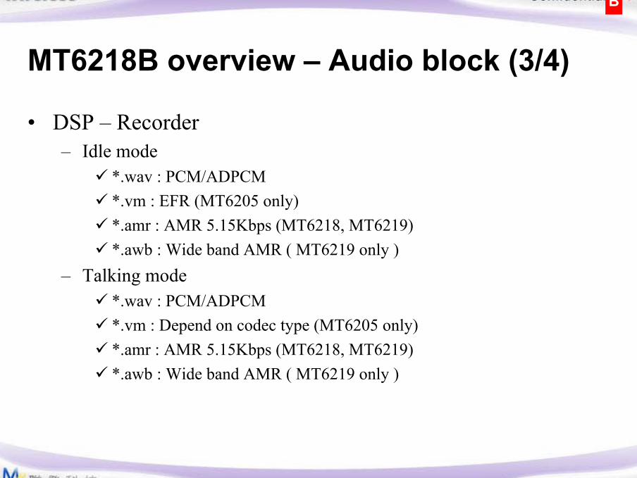
MT6218B overview – Audio block (3/4)
• DSP – Recorder– Idle mode
*.wav : PCM/ADPCM*.vm : EFR (MT6205 only) *.amr : AMR 5.15Kbps (MT6218, MT6219)*.awb : Wide band AMR ( MT6219 only )
– Talking mode*.wav : PCM/ADPCM*.vm : Depend on codec type (MT6205 only)*.amr : AMR 5.15Kbps (MT6218, MT6219)*.awb : Wide band AMR ( MT6219 only )

B
DAC
DAC MU
XM
UX
MU
X
Audio Amp-L
Audio Amp-R
Voice Amp-0
Voice Amp-1
AU-MOUTL
AU-MOUTR
AU-OUT0_N
AU-OUT0_P
AU-OUT1_P
AU-OUT1_N
Melody LMelody L + R
SpeechFM LFM L + R
Melody RMelody L + RSpeechFM R
FM L + R
Speech
Speech
Melody L + R
FM L + R
Speech
Melody
*.wav, *.mp3, *.mid, *.aac
*.wav *.vm*.amr*.wamr
FM Radio
EQ for MIDI
FIR
Recording
S.W.
-22dB ~ 23dB
-22dB ~ 23dB
-22dB ~ 8dB
-22dB ~ 8dB
MT6218B overview – Audio block (4/4)
0dBm0 : 0.6 Vrms
0dBm0 : 0.6 Vrms

B
Uplink/Downlink PGA gain setting
Voice Amp 0/1 Audio Amp L/R
0.6Vrms0.6Vrms0.2Vrms0dBm0
-22~8dB-22~23dB0~42dBTunable Range
2dB3dB2dBStep size
Downlink PGA gainUplink PGA gain
16 (2dB)16 (3dB)16 (2dB)Step size
0~2550~2550~255Tunable Range
SpeechMelodyMicrophoneEngineer modeEnter *#3646633# Audio Normal mode/ Headset mode/LoudSp mode

B
Application circuit discussion
• EMI & NFI & Memory Card– Camera – LCM – NOR Flash – NAND Flash – SRAM– MMC/SD/MS/MSPro
• Power & Charger function• Accessory Detection• Audio
• USB• Keypad• SIM • PWM• Alerter• Test point

B
MT6218 B+ Camera Module (Configuration 1)
~ 20wiresfor single LCD
Camera Module NANDFlash
SRAMOr
PseudoSRAM
NORFlash
MainLCD
Graphic SystemMaster
DMAMaster
LCDMaster
SYSRAM NAND FlashLCD
Interface
DSPShareRAM
EMI
USB
AHB2APBBridge
AHB2APBBridge
MCU
GPT
SIM
UARTs
TDMA
RTC
AFC
APC
ASI
RPI
DM
PM
CM
MCU Bus
DMA Bus
AP
B B
us
ResizerJPEG
Decoder
MCI
MT6218B
MemoryCard
PMIC6318
DRV
• Camera Module attached to LCD interface
• Suitable for Clam Shell phone with Camera mounted on upper cover
AITBE
B
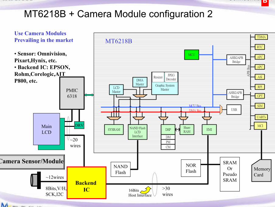
MT6218B + Camera Module configuration 2
NANDFlash
SRAMOr
PseudoSRAM
NORFlash
MainLCD
Backend IC
Graphic SystemMaster
DMAMaster
LCDMaster
SYSRAM NAND FlashLCD
Interface
DSPShareRAM
EMI
USB
AHB2APBBridge
AHB2APBBridge
MCU
GPT
SIM
UARTs
TDMA
RTC
AFC
APC
ASI
RPI
DM
PM
CM
MCU Bus
DMA Bus
AP
B B
us
ResizerJPEG
Decoder
MCI
MT6218B
MemoryCard
~20 wires
16BitsHost Interface
8Bits,V/H,SCK,I2C
~12wires
PMIC6318
DRV
>30 wires
Use Camera Modules Prevailing in the market
• Sensor: Omnivision, Pixart,Hynix, etc.• Backend IC: EPSON, Rohm,Corelogic,AIT P800, etc.
Camera Sensor/Module
B
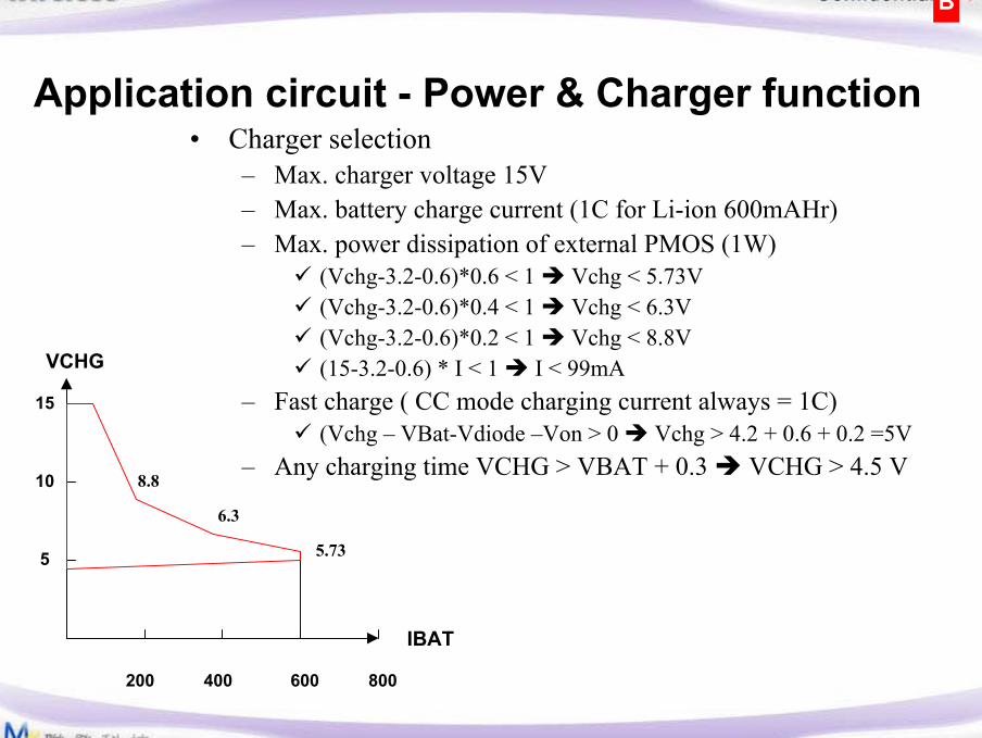
Application circuit - Power & Charger function• Charger selection
– Max. charger voltage 15V– Max. battery charge current (1C for Li-ion 600mAHr)– Max. power dissipation of external PMOS (1W)
(Vchg-3.2-0.6)*0.6 < 1 Vchg < 5.73V(Vchg-3.2-0.6)*0.4 < 1 Vchg < 6.3V(Vchg-3.2-0.6)*0.2 < 1 Vchg < 8.8V(15-3.2-0.6) * I < 1 I < 99mA
– Fast charge ( CC mode charging current always = 1C)(Vchg – VBat-Vdiode –Von > 0 Vchg > 4.2 + 0.6 + 0.2 =5V
– Any charging time VCHG > VBAT + 0.3 VCHG > 4.5 V
IBAT
VCHG
200 400 800600
5
10
15
5.73
6.3
8.8

B
Application circuit - Power & Charger function
• AUXADC circuit– Rsense, BATEMP curve, ENVTMP curve
ENVTMP
BATID
BATEMP
/2ISNESE
/2/5
VCHG
VBAT
R R R
MUX
ADC
AVDD
Rsense
RTRTR
Reserved

B
Application circuit - Power & Charger function
• Enter *#3646633# device Set default level battery– LEV1 : Power off – LEV2 : Transmit disable– LEV3 : Low battery alarm– LEV4 : Battery level 0 1– LEV5 : Battery level 1 2– LEV6 : Battery level 2 3

B
1. Check ADC fail,
2. Safety timer timeout (6hr)
3. Charger plugged out
Precharge state
Chargecomplete
state
Fast (CC)charge
state
Top-off (CV)charge state
Init state
Any state
Charger detected
Vbat_off > 3.4V
Vbat_off > 4.11V
ICHG < 120mA
Pause state
Vbat_off >4.05V and in talking mode
Vbat_off < 3.8V or in stand by
mode
Vbat_off < 4.1VVbat_off >4.05V and in talking mode
Vbat_off >4.05V and in talking mode
ADC check for abnormal condition
a. Vbat > 4.5V Battery over voltage
b. Vchg > 6.5 or Vchg < 3 Invalid charger
c. BATEMP < 0oC or BATEMP > 45oC Battery temp. too cold or over heat
d. BATID N.A.
e. ICHGon > 1A or ICHGon < 20mA Invalid charger or battery
f. ICHGoff > 1A Charger fail
P.S. XXX_on : ADC value is measured during pulse on charging and RF off state.
xxx_off : ADC value is measured during pulse off charging and RF off state.
xxx : ADC value is measured during pulse on and pulse off charging and RF off state.
Charge Error/end
state
Init safety timer
Vbat_off >4.05V and in talking mode
S.W. charging algorithm
Application circuit - Power & Charger function
Charger task MMICharger in
USB Charger inCharger out
USB Charger outADC fail
Charging time outCharge complete
OV=0(PMIC)

B
• S.W. protection mechanism for charging – 0 < BATEMP < 50 degree C (from battery spec.)– 4.5 < VCHG < 6.5 V (from PMIC spec. and charger spec.)– ICHG < 800mA (from charger & battery spec.)– BATID (N.A.)– OV (VBAT > 4.5V) (from battery spec.)– Safety timer 6Hr
Application circuit - Power & Charger function

B
ADC calibration and measurement
• 2 channel ADC calibration is a must.–Worse case下如不做calibration, charging current 在4.2V會有 4.2 *
(101/200-99/200) * 2 / 0.33 = 250mA 的誤差, 會使得電池永遠都充不飽
–ADC calibration. summary如下.a. calibration VBAT 3.4/4.2 兩點在ADC channel 0 and channel 3 b. ADC channel 1,2,4 的slope/offset直接copy ADC0
• 請特別注意只要ADC(10bits) cailbration有正負1個bit的誤差即會產生2.8/1024*2/0.33 * 2 = 34mA
• 建議ADC pass criterion 為–1. ADC0 : test at 3.6V +-40mV (等factory有大量資料後再做修正)–2. ADC3-ADC0/0.33 > 20mA (等factory有大量資料後再做修正)

B
Application circuit - RTC function
• For S.W. power on latch (power on key detection)– VRTC > 0.8V is a must ( 0.8V is a minimal working voltage of RTC block)– 2 sec debounce time (first power on)
• RTC charging current < 1~5mA (from PMIC spec.)– If charge current > 1mA, Vrtc will have a big drop. In order to complete a
normal power on @ RTC cap deep discharge. RTC charging current < 1mA is a must
• RTC charge current must be limited to 1.5V/4K = 0.375mA– Vrtccap maximal rising time = 40mF * 0.8/ 0.375 mA = 85 sec– Vrtcap full charging time = 160 sec. Stand by time > 10Hr
Vrtc
RTC blockPMIC4K
B
Application circuit - Accessory detection
• Bottom connector (Download cable/Earphone)– One interrupt pin is used to detect accessory plugged in/out.– One ADC channel is used to detect accessory ID.
• Earphone Jack– One interrupt pin is used to detect accessory plugged in/out.– One ADC channel is used to detect accessory ID.
• USB & Charger– 2 Interrupt– 1 interrupt + 1 ADC

B
Application circuit discussion - Audio
• External audio device configuration
StereoStereo4
MonoStereo3
StereoMono2
MonoMono1
Louder speakerEarphoneCase
AU-MOUTL
Stereo Earphone
AU-MOUTR
AU-OUT1_P
Case 3 Stereo Mono
Case 4 Stereo Stereo
AU-MOUTR
AU-MOUTL

B
Application circuit discussion - Audio
• Audio Gain budget planning – Earphone : External 430 ohm is suggested
Externalresister 430ohm
Vpp ofearphone
Powerdissapation ofearphone
dBm0 Vrms(V) Vpp(V)PGAGain Vpp(V) Setting
Gain(dB)
Vpp(V)430
Vpp(V)430
-3 0.424767471 1.201423836 -22 0.095432487 0 -23.1898399 0.006610042 0.000170674
-3 0.424767471 1.201423836 -19 0.134801972 16 -23.1898399 0.009336933 0.00034054
-3 0.424767471 1.201423836 -16 0.190412846 32 -23.1898399 0.013188769 0.000679467
-3 0.424767471 1.201423836 -13 0.268965294 48 -23.1898399 0.018629631 0.001355715
-3 0.424767471 1.201423836 -10 0.379923576 64 -23.1898399 0.026315053 0.002705008
-3 0.424767471 1.201423836 -7 0.536656315 80 -23.1898399 0.037171 0.0053972
-3 0.424767471 1.201423836 -4 0.758047193 96 -23.1898399 0.052505433 0.01076883
-3 0.424767471 1.201423836 -1 1.070770121 112 -23.1898399 0.074165896 0.021486641
-3 0.424767471 1.201423836 2 1.512502997 128 -23.1898399 0.104762112 0.042871485
-3 0.424767471 1.201423836 5 2.13646727 144 -23.1898399 0.147980417 0.085539859
-3 0.424767471 1.201423836 8 3.017840231 160 -23.1898399 0.209027895 0.170674456
-3 0.424767471 1.201423836 11 4.26281263 176 -23.1898399 0.295259749 0.340540311
-3 0.424767471 1.201423836 14 6.021382886 192 -23.1898399 0.417065481 0.679467249
-3 0.424767471 1.201423836 17 8.505429397 208 -23.1898399 0.589120651 1.355715396
-3 0.424767471 1.201423836 20 12.01423836 224 -23.1898399 0.832155038 2.705007839
-3 0.424767471 1.201423836 23 16.97056275 240 -23.1898399 1.175450234 5.397200202
Digital output Analog PGA
Reserved for speech
Single-end 2.8V Differential 5.6V

B
Application circuit discussion - Audio
• Audio Gain budget planning– Louder speaker ( External amp. Gain = 8 is suggested)
dBm0 Vrms(V) Vpp(V)PGAGain Vpp(V) Setting
Gain(dB)
Gain(dB)
Gain(dB)
Gain(dB)
Vpp(V)24
Vpp(V)18
Vpp(V)12
Vpp(V) 6
-3 0.42476747 1.2014238 -22 0.095432487 0 24 18 12 6 1.512502997 0.758047193 0.379923576 0.190412846
-3 0.42476747 1.2014238 -20 0.120142384 16 24 18 12 6 1.904128458 0.954324875 0.478295444 0.23971557
-3 0.42476747 1.2014238 -18 0.1512503 32 24 18 12 6 2.397155704 1.201423836 0.602138289 0.301784023
-3 0.42476747 1.2014238 -16 0.190412846 48 24 18 12 6 3.017840231 1.512502997 0.758047193 0.379923576
-3 0.42476747 1.2014238 -14 0.23971557 64 24 18 12 6 3.799235756 1.904128458 0.954324875 0.478295444
-3 0.42476747 1.2014238 -12 0.301784023 80 24 18 12 6 4.782954438 2.397155704 1.201423836 0.602138289
-3 0.42476747 1.2014238 -10 0.379923576 96 24 18 12 6 6.021382886 3.017840231 1.512502997 0.758047193
-3 0.42476747 1.2014238 -8 0.478295444 112 24 18 12 6 7.580471929 3.799235756 1.904128458 0.954324875
-3 0.42476747 1.2014238 -6 0.602138289 128 24 18 12 6 9.543248745 4.782954438 2.397155704 1.201423836
-3 0.42476747 1.2014238 -4 0.758047193 144 24 18 12 6 12.01423836 6.021382886 3.017840231 1.512502997
-3 0.42476747 1.2014238 -2 0.954324875 160 24 18 12 6 15.12502997 7.580471929 3.799235756 1.904128458
-3 0.42476747 1.2014238 0 1.201423836 176 24 18 12 6 19.04128458 9.543248745 4.782954438 2.397155704
-3 0.42476747 1.2014238 2 1.512502997 192 24 18 12 6 23.97155704 12.01423836 6.021382886 3.017840231
-3 0.42476747 1.2014238 4 1.904128458 208 24 18 12 6 30.17840231 15.12502997 7.580471929 3.799235756
-3 0.42476747 1.2014238 6 2.397155704 224 24 18 12 6 37.99235756 19.04128458 9.543248745 4.782954438
-3 0.42476747 1.2014238 8 3.017840231 240 24 18 12 6 47.82954438 23.97155704 12.01423836 6.021382886
Digital output Analog PGA External Loud Speaker Amp.
Reserved for speech
Single-end 2.8V Differential 5.6V

B
Connect to Driver• Audio driver
– mcu\custom\audio\XXXX_BB\audcoeff.c– mcu\custom\audio\XXXX_BB\nvram_default_audio.c
• Charging Parameter– mcu\custom\drv\misc_drv\XXXX_BB\chr_parameter.c
• Flash Range Configuration– mcu\custom\flash\XXXX_BB\FlashConf.c
• GPIO– mcu\custom\drv\misc_drv\XXXX_BB\gpio_drv.c
• ADC channel assignment– mcu\custom\drv\misc_drv\XXXX_BB\adc_channel.c
• EINT channel assignment– mcu\custom\drv\misc_drv\XXXX_BB\eint_def.c
• Keypad net definition– mcu\custom\drv\misc_drv\XXXX_BB\keypad_def.c
• PWM and Battery level parameters– mcu\custom\drv\misc_drv\custom_hw_default.c
B
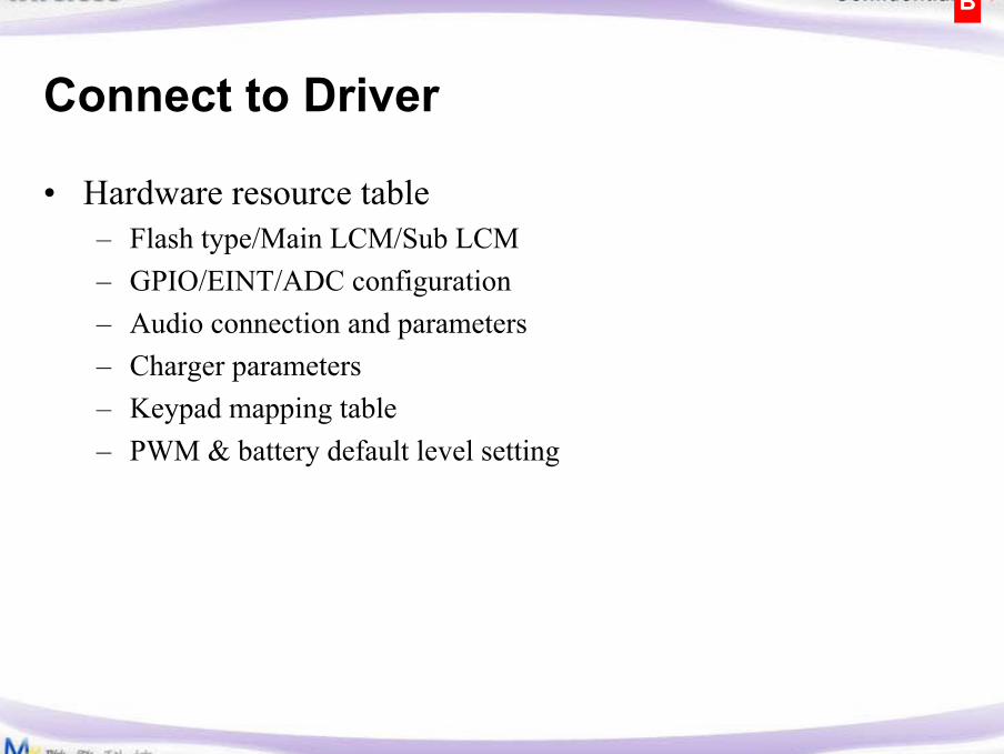
Connect to Driver
• Hardware resource table– Flash type/Main LCM/Sub LCM– GPIO/EINT/ADC configuration– Audio connection and parameters– Charger parameters– Keypad mapping table– PWM & battery default level setting
B
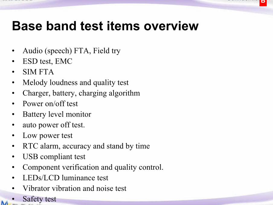
Base band test items overview
• Audio (speech) FTA, Field try• ESD test, EMC• SIM FTA • Melody loudness and quality test • Charger, battery, charging algorithm • Power on/off test • Battery level monitor• auto power off test. • Low power test• RTC alarm, accuracy and stand by time• USB compliant test• Component verification and quality control.• LEDs/LCD luminance test • Vibrator vibration and noise test • Safety test

B
Base band related tools overview• Target
– Factory mode (Enter *#66*#) (MMI test station)– Engineer mode (Enter *#3646633#)
– Speech UL/DL gain, side tone (normal mode, headset mode, hand free mode)– Echo suppressor– Melody gain setting– Key tone gain setting– Hardware control and monitor– ….
• Fast download tool– Code download
• Meta tools– ADC calibration (Calibration station)– Melody EQ fine tune – Speech parameter setting for FTA (PGA gain, FIR filter)
• Hardware test tool– AT command based (MMI test station)– Base band function test for factory– Hardware control for engineer
B
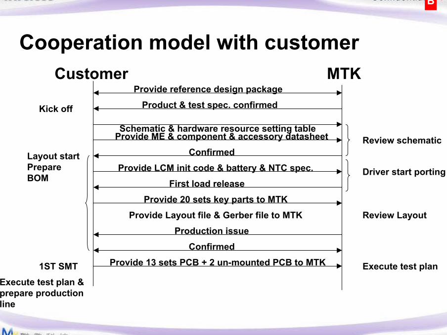
Cooperation model with customerMTKCustomer
Product & test spec. confirmed
Schematic & hardware resource setting table
ConfirmedProvide ME & component & accessory datasheet
Layout start Prepare BOM
Kick off
Review schematic
Provide reference design package
Provide LCM init code & battery & NTC spec. Driver start porting First load release
Provide 20 sets key parts to MTKReview LayoutProvide Layout file & Gerber file to MTK
ConfirmedProduction issue
1ST SMT Provide 13 sets PCB + 2 un-mounted PCB to MTK Execute test planExecute test plan & prepare production line
B
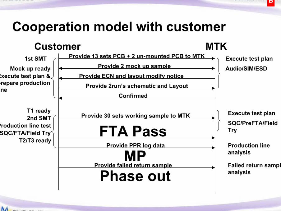
Cooperation model with customerMTKCustomer
Provide 2 mock up sample
Provide 2run’s schematic and LayoutConfirmed
Provide ECN and layout modify notice
Provide 30 sets working sample to MTK
Provide PPR log data
Provide failed return sample
Mock up ready Audio/SIM/ESD1st SMT Provide 13 sets PCB + 2 un-mounted PCB to MTK Execute test plan
Execute test plan & prepare production line
2nd SMTT1 ready Execute test plan
SQC/PreFTA/Field Try
Production line testSQC/FTA/Field Try FTA Pass
Production line analysisMPFailed return sample analysisPhase out
T2/T3 ready

专注于微波、射频、天线设计人才的培养 易迪拓培训 网址:http://www.edatop.com
射 频 和 天 线 设 计 培 训 课 程 推 荐
易迪拓培训(www.edatop.com)由数名来自于研发第一线的资深工程师发起成立,致力并专注于微
波、射频、天线设计研发人才的培养;我们于 2006 年整合合并微波 EDA 网(www.mweda.com),现
已发展成为国内最大的微波射频和天线设计人才培养基地,成功推出多套微波射频以及天线设计经典
培训课程和 ADS、HFSS 等专业软件使用培训课程,广受客户好评;并先后与人民邮电出版社、电子
工业出版社合作出版了多本专业图书,帮助数万名工程师提升了专业技术能力。客户遍布中兴通讯、
研通高频、埃威航电、国人通信等多家国内知名公司,以及台湾工业技术研究院、永业科技、全一电
子等多家台湾地区企业。
易迪拓培训课程列表:http://www.edatop.com/peixun/rfe/129.html
射频工程师养成培训课程套装
该套装精选了射频专业基础培训课程、射频仿真设计培训课程和射频电
路测量培训课程三个类别共 30 门视频培训课程和 3 本图书教材;旨在
引领学员全面学习一个射频工程师需要熟悉、理解和掌握的专业知识和
研发设计能力。通过套装的学习,能够让学员完全达到和胜任一个合格
的射频工程师的要求…
课程网址:http://www.edatop.com/peixun/rfe/110.html
ADS 学习培训课程套装
该套装是迄今国内最全面、最权威的 ADS 培训教程,共包含 10 门 ADS
学习培训课程。课程是由具有多年 ADS 使用经验的微波射频与通信系
统设计领域资深专家讲解,并多结合设计实例,由浅入深、详细而又
全面地讲解了 ADS 在微波射频电路设计、通信系统设计和电磁仿真设
计方面的内容。能让您在最短的时间内学会使用 ADS,迅速提升个人技
术能力,把 ADS 真正应用到实际研发工作中去,成为 ADS 设计专家...
课程网址: http://www.edatop.com/peixun/ads/13.html
HFSS 学习培训课程套装
该套课程套装包含了本站全部 HFSS 培训课程,是迄今国内最全面、最
专业的HFSS培训教程套装,可以帮助您从零开始,全面深入学习HFSS
的各项功能和在多个方面的工程应用。购买套装,更可超值赠送 3 个月
免费学习答疑,随时解答您学习过程中遇到的棘手问题,让您的 HFSS
学习更加轻松顺畅…
课程网址:http://www.edatop.com/peixun/hfss/11.html
`

专注于微波、射频、天线设计人才的培养 易迪拓培训 网址:http://www.edatop.com
CST 学习培训课程套装
该培训套装由易迪拓培训联合微波 EDA 网共同推出,是最全面、系统、
专业的 CST 微波工作室培训课程套装,所有课程都由经验丰富的专家授
课,视频教学,可以帮助您从零开始,全面系统地学习 CST 微波工作的
各项功能及其在微波射频、天线设计等领域的设计应用。且购买该套装,
还可超值赠送 3 个月免费学习答疑…
课程网址:http://www.edatop.com/peixun/cst/24.html
HFSS 天线设计培训课程套装
套装包含 6 门视频课程和 1 本图书,课程从基础讲起,内容由浅入深,
理论介绍和实际操作讲解相结合,全面系统的讲解了 HFSS 天线设计的
全过程。是国内最全面、最专业的 HFSS 天线设计课程,可以帮助您快
速学习掌握如何使用 HFSS 设计天线,让天线设计不再难…
课程网址:http://www.edatop.com/peixun/hfss/122.html
13.56MHz NFC/RFID 线圈天线设计培训课程套装
套装包含 4 门视频培训课程,培训将 13.56MHz 线圈天线设计原理和仿
真设计实践相结合,全面系统地讲解了 13.56MHz线圈天线的工作原理、
设计方法、设计考量以及使用 HFSS 和 CST 仿真分析线圈天线的具体
操作,同时还介绍了 13.56MHz 线圈天线匹配电路的设计和调试。通过
该套课程的学习,可以帮助您快速学习掌握 13.56MHz 线圈天线及其匹
配电路的原理、设计和调试…
详情浏览:http://www.edatop.com/peixun/antenna/116.html
我们的课程优势:
※ 成立于 2004 年,10 多年丰富的行业经验,
※ 一直致力并专注于微波射频和天线设计工程师的培养,更了解该行业对人才的要求
※ 经验丰富的一线资深工程师讲授,结合实际工程案例,直观、实用、易学
联系我们:
※ 易迪拓培训官网:http://www.edatop.com
※ 微波 EDA 网:http://www.mweda.com
※ 官方淘宝店:http://shop36920890.taobao.com
专注于微波、射频、天线设计人才的培养
官方网址:http://www.edatop.com 易迪拓培训 淘宝网店:http://shop36920890.taobao.com