automatic multi storied car parking system report
DESCRIPTION
automatic multi storied car parkingTRANSCRIPT

Chapter 1
Introduction
1.1 Introduction
Automatic multi storied car parking system helps to minimize the car parking area. In the
modern world, where parking-space has become a very big problem and in the era of
miniaturization, it is become a very crucial necessity to avoid the wastage of space in modern,
big companies and apartments etc. In places where more than 100 cars need to be parked, this
system proves to be useful in reducing wastage of space. This Automatic Car Parking System
enables the parking of vehicles, floor after floor and thus reducing the space used. Here any
number of car scan be parked according to the requirement. This makes the system modernized
and even a space-saving one. This idea is developed using 8051 Microcontroller. Here program
is written according to this idea using 8051.
1.2 Basic idea
A display is provided at the ground floor which is basically a counter that displays number of
cars in each floor. It informs whether the floors are fully filled with the cars or is it having place
in a particular floor or not. In this project we have provided three floors of a building for car
parking. Maximum storage capacity of each floor is given as five. Storage capacity can be
changed according to the requirement. As soon as a car is placed in a particular floor, the display
counter at the ground floor increments as to indicate the floor capacity has decreased by one.
We are using two light sensors at each floor( one at the entrance and one at the exit) which sense
the presence of car and tell the counter to decrease or increase.The project has been divided into
following sections:-
1. Display section
2. Indicator & Beeper section
3. Sensor section
4. LCD section
1.2.1 Display section
1

This section displays the floor number along with the number of cars which has been already
parked in that particular floor. So whenever a car is ready to either come down or go up the
program either decrements the count or increments the count automatically according to the
going up or coming down of a car. Display section is done by interfacing with 8255(PPI) of
8051.Here 3 ports of 8255 are connected to three 7-segment display.
1.2.2 Indicator & beeper
When a person tries to enter the lift irrespective of finding the display section to be 05 (means
the floors are already filled), program sends a signal to Beeper and indicator section and it starts
beeping indicating that he is not supposed to enter the lift since all the floors are already filled.
1.2.3 Sensor section
Here we have used 2 light sensors (LED $ LDR) at each floor. One is for the entrance and
another for exit. In normal condition the light from LED is sensed by the LDR but when a car
comes in between the transmitter (LED) and receiver (LDR) the LDR does not receive any light
and its output changes accordingly which is sent to the microcontroller which hence increment or
decrement the value of the counter.
1.2.4 LCD Section
In this project LCD is used to display some messages which is useful to car owners. Here 2X16
LCD (Liquid Crystal Display) is used. This is used to display messages like
WELCOME TO CAR PARKING SYSTEM
FLOOR IS FULL
1.3 Block Diagram
2

Figure 1.1
Block Diagram of Project
3

Chapter 2
Project Overview
2.1 Circuit Diagram
Figure 2.1
Circuit diagram
4

4.2 Circuit Description
The controlling part of the system is 8051 microcontroller. There are 6 sensors, two mounted on
each floor(one for entrance and one for exit). The sensors are mounted in through bea
configuration. When a car comes in between the sensor transmitter and receiver the output of the
sensor becomes 0. This output is given to the microcontroller. The programming is done in such
a way that whenever the output of a sensor changes from 1 to 0 the counter value gets increase or
decrease (depending on where the sensor is i.e.: at entrance or at exit).
The latch (74HCT373) is provided to demultiplex the higher order address lines of the
microcontroller. The data lines are used to fetch data to the 8255 and the address lines
(demultiplexed) are used for the chip select of the 8255. The chip selection of the 8255 is done
by using an 8 input nand gate (74HC30) and a 3-8 decoder(74HC138).
There are 3 seven segment display (LT542) used here, each for showing number of cars
parked at a floor. The LCD is used to display some meaningful messages. The displays are
connected to ane 8255 and the LCD to another one.
5

Chapter 3
Components Description
3.1 Components List
S.
NO.
Name of
Component
Specifications Quantity PRICE TOTAL
COST
1 Resistors 330 12 2
10 k 12 2
8.2 k 1 1
2 Capacitors 10 µf 1 1 2
33 pf 2 1 2
3 IC LM324 2 10 20
AT89S52 1 60 60
74HCT373 1 20 20
8255A 2 60 120
74HC30 1 20 20
74HC138 1 20 20
4 LDR 6 8 48
5 LED 12 1 12
6 7 Segment Display LT542 3 10 30
7 LCD 12 X 7 1 150 150
8 Crystal Oscillator 24 MHz 1
9 Variable Resistor 20 k 6 3 18
Table 3.1
Components List
3.2 8051 Microcontroller(AT89S52)
6

The 8051 microcontroller generic part number actually includes a whole family of
microcontrollers that have numbers ranging from 8031 to 8751.The block diagram of the
8051shows all of the features unique to microcontrollers:
Internal ROM and RAM· I/O ports with programmable pins· Timers and counters. Serial data
communication The block diagram also shows the usual CPU components program counter,
ALU, working registers, and the clock circuits.
The 8051 architecture consists of these specific features:·
8 bit CPU with registers A and B
16 bit PC &data pointer (DPTR)
8 bit program status word (PSW)
8 bit stack pointer(SP)
Internal ROM or EPROM (8751)of 0(8031)to 4k(8051)
Internal RAM of 128 bytes
4 register banks, each containing 8 registers
80 bits of general purpose data memory
32 input/output pins arranged as four 8 bit ports:P0-P3
Two 16 bit timer/counters:T0-T1
Two external and three internal interrupt sources
Oscillator and clock circuits
A pin out of the 8051 packaged in a 40 pin DIP is shown below
7

Figure 3.1
8051 microcontroller
3.3 8255 PPI
The 8255A programmable peripheral interface (PPI) implements a general-purpose I/O interface
to connect peripheral equipment to a microcomputer system bus. The core's functional
configuration is programmed by the system software so that external logic is not required to
interface peripheral devices. Its has following features
Three 8-bit Peripheral Ports - Ports A, B, and C
Three programming modes for Peripheral Ports: Mode 0 (Basic Input/Output), Mode
1 (Strobed Input/Output), and Mode 2 (Bidirectional)
Total of 24 programmable I/O lines
8-bit bidirectional system data bus with standard microprocessor interface controls
8

3.4 3-8 Decoder(74HCT138)
The 74HC138; 74HCT138 is a high-speed Si-gate CMOS device and is pin compatible with
Low-power Schottky TTL (LSTTL). It accepts three binary weighted address inputs (A0, A1
and A3) and when enabled, provides 8 mutually exclusive active LOW outputs (Y0 to Y7). It
features three enable inputs: two active LOW (E1 and E2) and one active HIGH (E3). Every
output will be HIGH unless E1 and E2 are LOW and E3 is HIGH.
The 74HC138; 74HCT138 can be used as an eight output demultiplexer by using one of
the active LOW enable inputs as the data input and the remaining enable inputs as strobes. Not
used enable inputs must be permanently tied to their appropriate active HIGH- or LOW-state. It
ha following features:-
Demultiplexing capability
Multiple input enable for easy expansion
Complies with JEDEC standard no. 7A
Ideal for memory chip select decoding
Active LOW mutually exclusive outputs
ESD protection:
Specified from −40 °C to +85 °C and from −40 °C to +125 °C
Figure 3.2
74HCT138
9

3.5 Latch(74HC373)
The 74HC373; 74HCT373 is a high-speed Si-gate CMOS device and is pin compatible with
Low-power Schottky TTL. It is specified in compliance with JEDEC standard no. 7A. It is an
octal D-type transparent latch featuring separate D-type inputs for each latch and 3-state outputs
for bus oriented applications. A latch enable (LE) input and an output enable (OE) input are
common to all latches.
The 74HC373; 74HCT373 consists of eight D-type transparent latches with 3-state true
outputs. When LE is HIGH, data at the Dn inputs enters the latches. In this condition the latches
are transparent, i.e. a latch output will change state each time its corresponding D input changes.
When LE is LOW the latches store the information that was present at the D inputs a set-up time
preceding the HIGH-to-LOW transition of LE. When OE is LOW, the contents of the 8 latches
are available at the outputs. When OE is HIGH, the outputs go to the high-impedance OFF-state.
Operation of the OE input does not affect the state of the latches. It has following features and
benefits:-
3-state non-inverting outputs for bus oriented applications
Common 3-state output enable input
Functionally identical to the 74HC563; 74HCT563 and 74HC573; 74HCT573
ESD protection:
Specified from −40 °C to +85 °C and from −40 °C to +125 °C
Figure 3.3
74HC373
10

3.6 Nand Gate IC(74HC30)
The 74HC30; 74HCT30 are high-speed Si-gate CMOS devices that comply with JEDEC
standard no. 7A. They are pin compatible with Low-power Schottky TTL (LSTTL). The
74HC30; 74HCT30 provides a quad 8-input NAND function. It has following features and
benefits:-
Input levels:
o For 74HC30: CMOS level
o For 74HCT30: TTL level
ESD protection:
Multiple package options
Specified from −40 °C to +85 °C and from −40 °C to +125 °C
Figure 3.4
74HC30
11

3.7 Resistors
Resistors are the electronic components which opposes current. Resistors obey ohm law.
Different kind of result comes with respect to application of various voltages.
Figure 3.5
Resistor
3.8 Capacitors
A capacitor is an electrical or electronics device that can store energy the electric field between a
pair of conductors. This process of storing energy field between a pair of conductors. The
process of storing energy is called charging. A 47microF 25v capacitor is used.
Figure 3.6
Capacitor
12

Chapter 4
Software Used
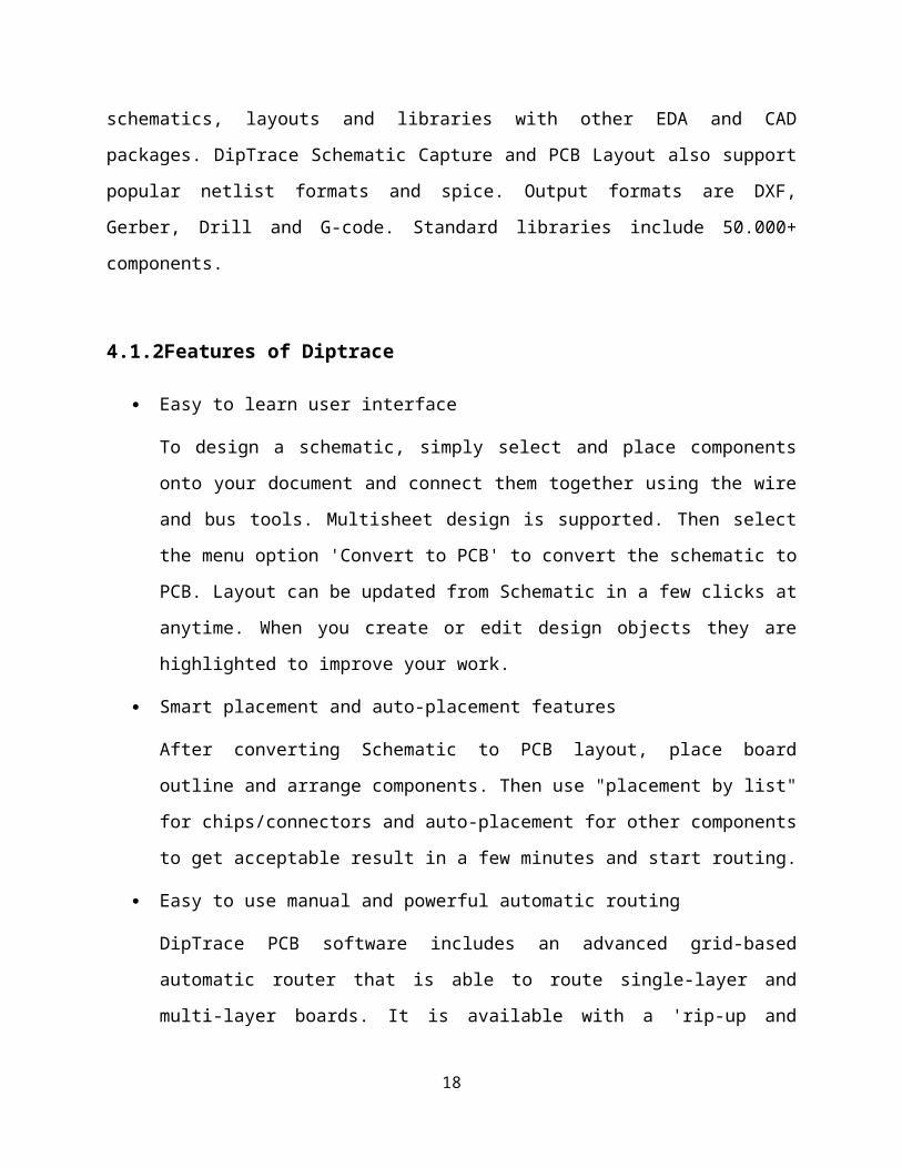
4.1 Diptrace
4.1.1 Role In The Design
Dip Trace 1.5 proved to be a very handy & easy-to-use tool for the PCB layout process. Many of
its features were utilized leading to an accurate & efficient design. It has Design Error Check &
Electrical Rule Check tools which proved to be helpful in the design. It is loaded with a huge
component list that is categorized in various libraries for giving simplicity. Placement of
components is also very easy & they can be rotated in 360 degree to customize the design.
DipTrace is an advanced PCB design software application that consists of 4 modules: PCB
Layout with efficient auto-router, Schematic Capture, Component and Pattern Editors that allow
you to design your own component libraries. Besides being very simple to learn, this software
has a very intuitive user interface and many innovative features. For instance, a schematic can be
converted to a PCB with one mouse click. Advanced manual placement and auto-placement
features allow to get acceptable placement in several minutes. The board designer can instantly
renew the PCB from an updated version of schematic and keep all previous work without
changes. PCB and Schematic can be compared at any design stage to ensure they are identical.
DipTrace has a powerful automatic router. It can route a single layer and multilayer circuit
boards, and there is an option to autoroute a single layer board with jumper wires, if required.
DipTrace also provides you with external autorouter support. Smart manual routing tools allow
users to finalize the design and to get the results they want in a blink of an eye. Accurate shape-
based copper pour system with different possible fill types and thermals can be used to make
planes or to reduce manufacturing costs. Other important features are Electrical Rule Check
(ERC), Design Rule Check (DRC) and Net Connectivity Check - the functions that check
connections in Schematic by different rules (pin type, short circuit, etc.), the clearance between
layout objects, which ensures board accuracy, and connectivity of all nets not depending on how
they are connected (with traces, thermals or shapes). DipTrace modules allow you to exchange
13

schematics, layouts and libraries with other EDA and CAD packages. DipTrace Schematic
Capture and PCB Layout also support popular netlist formats and spice. Output formats are
DXF, Gerber, Drill and G-code. Standard libraries include 50.000+ components.
4.1.2Features of Diptrace
Easy to learn user interface
To design a schematic, simply select and place components onto your document and
connect them together using the wire and bus tools. Multisheet design is supported. Then
select the menu option 'Convert to PCB' to convert the schematic to PCB. Layout can be
updated from Schematic in a few clicks at anytime. When you create or edit design
objects they are highlighted to improve your work.
Smart placement and auto-placement features
After converting Schematic to PCB layout, place board outline and arrange components.
Then use "placement by list" for chips/connectors and auto-placement for other
components to get acceptable result in a few minutes and start routing.
Easy to use manual and powerful automatic routing
DipTrace PCB software includes an advanced grid-based automatic router that is able to
route single-layer and multi-layer boards. It is available with a 'rip-up and retry'
algorithm. With Specctra DSN/SES interface you can use external shape-based or
topological autorouter. Intelligent manual routing tools allow you to create and edit traces
by 90, 45 degree or without any limitations. Curved traces are supported. Through, blind
or buried vias can be used in automatic and manual routing. Board size is not limited.
Shape-based copper pour
Powerful copper pour system can help to reduce your manufacturing costs by minimizing
the amount of etching solution required. To use it, all you have to do is insert a copper
area on your board in the PCB Layout program and any pad or trace inside the selected
area will be automatically surrounded with a gap of the desired size. Using copper pour
you can also create planes and connect them to pads and vias (different thermal types are
supported).
14

Advanced Verification Features
Schematic and PCB design modules have number of verification features that help
control project accuracy on different design stages: The ERC function shows possible
errors in Schematic pin connections using defined rules and allows you to correct errors
step-by-step. DRC function checks the clearance between design objects, minimum size
of traces, and drills. Errors are displayed graphically and you can fix them step-by-step
and rerun the DRC in one click after any corrections. Net Connectivity Check verifies if
all nets of PCB are electrically connected. This feature uses traces, copper pour filled area
and shapes to control connectivity, then reports broken and merged nets with area details.
Comparing to Schematic allows you to check if routed PCB is identical with Schematic.
Standard component libraries
DipTrace package includes component and pattern libraries which contain 90,000+
components from different manufacturers.
Creation of your own libraries
Component and Pattern Editors allow to design your own symbols and patterns. To create
complete components simply connect them together using Component Editor.
4.1.3 Circuit Layout
15
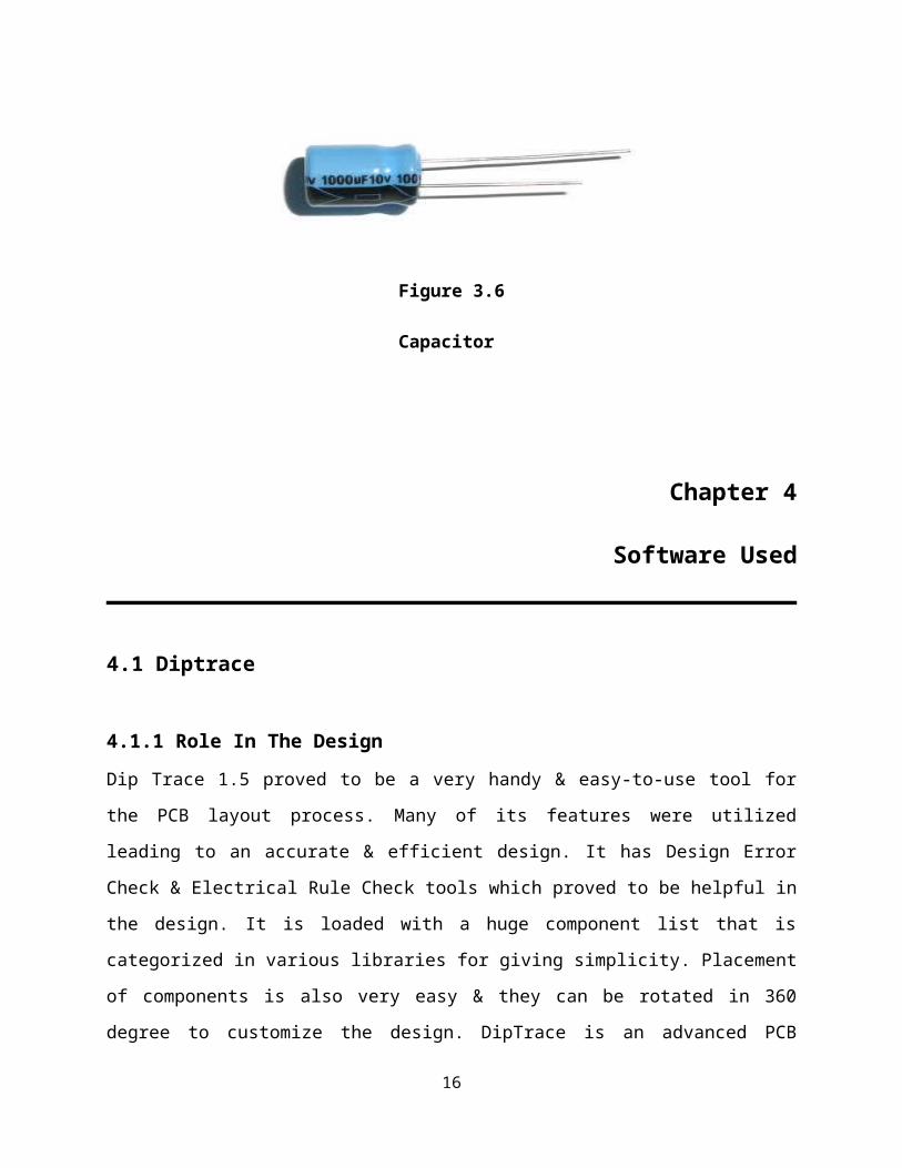
Figure 4.1
Diptrace Layout Of Circuit
16

Chapter 5
PCB Fabrication
5.1 Introduction
The process starts once your files and specifications have been sent to Triangle Circuits. Our
engineers review each order to ensure design for manufacturability and proper selection of
materials and technologies before manufacturing begins.
5.2 Patterning | Etching
The majority of printed circuit boards are manufactured by applying a layer of copper over the
entire surface of the circuit board substrate either on one side or both sides. This creates what is
referred to as a blank printed circuit board, meaning the copper is everywhere on the surface.
From here the unwanted areas are removed, this is called a subtractive method, the most
common subtractive method is known as photoengraving.
5.3 Photoengraving
The photoengraving process uses a mask or photo mask combined with chemical etching to
subtract the copper areas from the circuit board substrate Thephoto mask is created with a photo
plotter which takes the design from a CAD PCB software program. Lower resolution photo
masks are sometimes created with the use of a laser printer using a transparency.
5.4 Lamination
Many printed circuit boards are made up of multiple layers, these are referred to as multi-layer
printed circuit boards. They consist of several thin etched boards or trace layers and are bonded
together through the process of lamination.
5.5 Drilling
17
Each layer of the printed circuit board requires the ability of one layer to connect to another, this
is achieved through drilling small holes called "VIAS". These drilled holes require precision
placement and are most commonly done with the use of an automated drilling machine. Theses
machines are driven by computer programs and files called numerically controlled drill or
(NCD) files also referred to as excellon files. These files determine the position and size of each
file in the design.
Some files require very small vias to be drilled which results in heavy wear and tear of
the drill bit itself. Drilling through different substrates may require the drill bit to be made of
tungsten carbide and are costlier than other materials but required to provide a proper hole.
Controlled depth drilling can be used to drill just one layer of the circuit board rather than
drilling through all the layers. This can be accomplished by drilling the individual sheets or
layers of the PCB prior to lamination.
Blind Vias: Is when the holes connect a layer to the outside surface
Buried Vias: Is when the holes only connect interior layers and not to the outside surface.
5.6 Solder Plating | Solder Resist
Pads and lands which will require components to be mounted on are plated to allow solderability
of the components. Bare copper is not readily solderable and requires the surface to be plated
with a material that facilitates soldering. In the past a lead based tin was used to plate the
surfaces, but with RoHS compliance enacted newer materials are being used such as nickel and
gold to both offer solder ability and comply with RoHS standards.
Areas that should not be solderable are covered with a material to resist soldering. Solder
resist refers the a polymer coating that acts as a mask and prevents solder from bridging traces
and possibly creating short circuits to nearby component leads.
5.7 Silk Screen
18

When visible information needs to be applied to the board such as company logos, part numbers
or instructions, silk screening is used to apply the text to the outer surface of the circuit board.
Where spacing allows, screened text can indicate component designators, switch setting
requirements and additional features to assist in the assembly process.
5.8 Testing
Unpopulated circuit boards are subjected to a bare board test where each circuit connection (as
defined in a net list) is verified as correct on the finished circuit board. In high volume circuit
board production, a bed of nails tester or fixture is used to make contact with the copper lands or
holes on one or both sides of the board to facilitate testing. Computers are used to control the
electrical testing unit to send a small current through each contact point on the bed of nails and
verify that such current can be detected on the appropriate contact points.
For small to medium volume production runs, a flying probe tester is used to check
electrical contacts. These flying probes employ moving heads to make contact with the copper
lands and holes to validate the electrical connectivity of the board being tested.
Chapter 6
19

Coding
$MOD51
ORG 0000H
CLR P0.2;
CLR P0.3;
CLR P0.4;
CLR P0.5;
CLR P0.6;
CLR P2.1;
CLR P2.2;
CLR P2.3;
CLR P2.4;
r1=0;
r2=0;
r3=0;
MAIN:MOV C, P3.0;
JNC sensor1;
20

MOV C, P3.1;
JNC sensor2;
MOV C, P3.2;
JNC sensor3;
MOV C, P3.3;
JNC sensor4;
MOV C, P3.4;
JNC sensor5;
MOV C, P3.5;
JNC sensor6;
SJMP MAIN;
sensor1: CJNZ r1, #05H back12;
CLR P1.0;
CLR P1.1;
21

sensor3: CJNZ r2, #05H back34;
CLR P1.0;
CLR P1.1;
sensor1: CJNZ r3, #05H back56;
CLR P1.0;
CLR P1.1;
back12: INC r1;
ACALL display12;
back34: INC r2;
ACALL display34;
back56: INC r3;
ACALL display56;
sensor2: CJNZ r1, #00H back;
DCR r1;
ACALL display12;
22

sensor4: CJNZ r2, #00H back;
DCR r2;
ACALL display34;
sensor6: CJNZ r3, #00H back;
DCR r3;
ACALL display56;
display12: CLR P2.7;
CLR P2.6;
CLR P2.5;
MOV A, #01H;
SUB r1;
JZ display1A;
MOV A, #02H;
SUB r1;
JZ display2A;
MOV A, #03H;
23

SUB r1;
JZ display3A;
MOV A, #04H;
SUB r1;
JZ display4A;
MOV A, #05H;
SUB r1;
JZ display5A;
display34: CLR P2.7;
CLR P2.6;
CLR P2.5;
MOV A, #01H;
SUB r2;
JZ display1B;
MOV A, #02H;
SUB r2;
24

JZ display2B;
MOV A, #03H;
SUB r2;
JZ display3B;
MOV A, #04H;
SUB r2;
JZ display4B;
MOV A, #05H;
SUB r2;
JZ display5B;
display56: CLR P2.7;
CLR P2.6;
CLR P2.5;
MOV A, #01H;
SUB r3;
JZ display1C;
25

MOV A, #02H;
SUB r3;
JZ display2C;
MOV A, #03H;
SUB r3;
JZ display3C;
MOV A, #04H;
SUB r3;
JZ display4C;
MOV A, #05H;
SUB r3;
JZ display5C;
display1A: MOV A, #80H;
MOV DPTR, #7EFFH;
MOV X @DPTR, A;
MOV A, #0BEH;
26

MOV DPTR, #7EFCH;
MOV X @DPTR, A;
SJMP MAIN;
display2A: MOV A, #80H;
MOV DPTR, #7EFFH;
MOV X @DPTR, A;
MOV A, #0C4H;
MOV DPTR, #7EFCH;
MOV X @DPTR, A;
SJMP MAIN;
display3A: MOV A, #80H;
MOV DPTR, #7EFFH;
MOV X @DPTR, A;
MOV A, #94H;
MOV DPTR, #7EFCH;
MOV X @DPTR, A;
SJMP MAIN;
display4A: MOV A, #80H;
27

MOV DPTR, #7EFFH;
MOV X @DPTR, A;
MOV A, #0B2H;
MOV DPTR, #7EFCH;
MOV X @DPTR, A;
SJMP MAIN;
display1B: MOV A, #80H;
MOV DPTR, #7EFFH;
MOV X @DPTR, A;
MOV A, #7DH;
MOV DPTR, #7EFDH;
MOV X @DPTR, A;
SJMP MAIN;
display2B: MOV A, #80H;
MOV DPTR, #7EFFH;
MOV X @DPTR, A;
MOV A, #23H;
MOV DPTR, #7EFDH;
MOV X @DPTR, A;
28

SJMP MAIN;
display3B: MOV A, #80H;
MOV DPTR, #7EFFH;
MOV X @DPTR, A;
MOV A, #29H;
MOV DPTR, #7EFDH;
MOV X @DPTR, A;
SJMP MAIN;
display4B: MOV A, #80H;
MOV DPTR, #7EFFH;
MOV X @DPTR, A;
MOV A, #4DH;
MOV DPTR, #7EFDH;
MOV X @DPTR, A;
SJMP MAIN;
display5B: MOV A, #80H;
MOV DPTR, #7EFFH;
MOV X @DPTR, A;
29

MOV A, #89H;
MOV DPTR, #7EFDH;
MOV X @DPTR, A;
SJMP MAIN;
display1C: MOV A, #80H;
MOV DPTR, #7EFFH;
MOV X @DPTR, A;
MOV A, #0B7H;
MOV DPTR, #7EFEH;
MOV X @DPTR, A;
SJMP MAIN;
display2C: MOV A, #80H;
MOV DPTR, #7EFFH;
MOV X @DPTR, A;
MOV A, #0C2H;
MOV DPTR, #7EFEH;
MOV X @DPTR, A;
SJMP MAIN;
30

display3C: MOV A, #80H;
MOV DPTR, #7EFFH;
MOV X @DPTR, A;
MOV A, #92H;
MOV DPTR, #7EFEH;
MOV X @DPTR, A;
SJMP MAIN;
display4C: MOV A, #80H;
MOV DPTR, #7EFFH;
MOV X @DPTR, A;
MOV A, #0B4H;
MOV DPTR, #7EFEH;
MOV X @DPTR, A;
SJMP MAIN;
display5C: MOV A, #80H;
MOV DPTR, #7EFFH;
MOV X @DPTR, A;
MOV A, #98H;
MOV DPTR, #7EFEH;
31

MOV X @DPTR, A;
SJMP MAIN;
DELAY: MOV R0,#07H;
MAIN1: MOV R1,#0FFH;
MAIN2: MOV R2,#0FFH;
MAIN3: DJNZ R2, MAIN3;
DJNZ R1, MAIN2;
DJNZ R0, MAIN1;
RET;
END
Chapter 7
32

Applications and Future Scope
7.1 Applications
Automatic multi-storey car parks provide lower building cost per parking slot, as they typically
require less building volume and less ground area than a conventional facility with the same
capacity.
Costs are usually lower too, for example there is no need for an energy intensive ventilating
system, since cars are not driven inside and human cashiers or security personnel may not be
needed.
A multi-storey car parks offer greatest possible flexibility for the realization of optimum parking
solution.
A fast parking process in which the driver does not have to maneuver his car or drive backwards,
guarantees highest comfort and security.
It can be used in malls and other public places where space utilization is needed.
It can be used at the places where public events are commonly held.
7.2 Future Scope
Lift can be added to the system to improve the automatisation.
Security of the system can be improved by introducing entry through the passwords.
Automatic Gates can be provided at the entry and exit of each floor.
Conclusion
33

The Automated Multistoried Car Parking System can be proved to be a useful and successful
project for our country. It can be used in malls, auditoriums and other places where parking
requires less space and security, at the places where public events are commonly held or at the
places where VIP security is priority.
The system is designed keeping the every small thing which is required for a good
parking system, in mind so that it could become convenient for the people to deal with. Since the
system design is so flexible thus it is easy to use and maintain.
References
34

www.nxp.com/documents/data_sheet
www.atmel.com/atmel
http://en.wikipedia.org
http://www.google.co.in/
Architecture and Programming of 8051 Microcontrollers by Milan Verle
The 8051 Microcontroller and Embedded Systems Using Assembly and C-2nd-ed BY
Mazidi
35